


Low Power Precision Analog Microcontroller
ARM Cortex M3, with dual Sigma-Delta ADCs
ADuCM360/ADuCM361
Rev. Pr R
Information furnished by Analog Devices is believed to be accurate and reliable. However, no
Trademarks and registered trademarks are the property of their respective owners.
Fax: 781.461.3113 ©2012 Analog Devices, Inc. All rights reserved.
Preliminary Technical Data
FEATURES
Analog Input/Output
Dual (24-bit) ADCs (ADuCM360)
Single (24-bit) ADC (ADuCM361)
Single Ended and fully Differential inputs
Programmable ADC output rate (4 Hz to 4 kHz)
Simultaneous 50Hz/60Hz rejection
50SPS Continuous Conversion Mode
16.67SPS Single Conversion Mode
Flexible input MUX for input channel selection to both ADCs
Primary and Auxiliary (24-bit) ADC channel
6 differential or 11 Single-Ended input channels
4 internal channels for monitoring DAC, Temperature
sensor, IOVDD and AVDD (ADC1 only)
Programmable Gain (1 to 128)
Selectable input range: ±6.64 mV to ±1.2 V
RMS noise: 43nV @3.75Hz, 180nV @ 50Hz
Programmable sensor excitation current sources
10/50/100/150/200/250/300/400/500/600/800uA and
1mA current source options
On-chip precision Voltage reference (±4 ppm/°C)
Single 12-bit voltage output DAC
NPN mode for 4-20mA loop applications
Microcontroller
ARM Cortex™-M3 32-bit processor
Serial Wire download and debug
Internal Watch crystal for wakeup timer
16 MHz Oscillator with 8-way Programmable Divider
Memory
128k Bytes Flash/EE Memory, 8k Bytes SRAM
In-circuit debug/download via Serial Wire and UART
Power
Operates directly from a 3.0V battery
Supply Range: 1.8V to 3.6V (max)
Power Consumption
MCU Active Mode: Core consumes 290µA / MHz
Active Mode: 1.0mA (All peripherals active), core
operating at 500KHz
Power down mode: 4µA (WU Timer Active)
On-Chip Peripherals
UART, I2C and 2 x SPI Serial I/O
16-bit PWM Controller
19-Pin Multi-Function GPIO Port
2 General Purpose Timers
Wake -up Ti mer/Watchdog Timer
Multi-Channel DMA and Interrupt Controller
Package and Temperature Range
48 lead LFCSP (7mm x 7mm) package –40°C to 125°C
Development Tools
Low-Cost QuickStart™ Development System
Third-Party Compiler and emulator tool Support
Multiple Functional Safety features for improved diagnostics
APPLICATIONS
Industrial automation and process control
Intelligent, precision sensing systems
4 mA to 20 mA loop-powered smart sensor systems
Medical devices, patient monitoring
responsibility is assumed by Analog Devices for its use, nor for any infringements of patents or other
rights of third parties that may result from its use. Specifications subject to change without notice. No
license is granted by implication or otherwise under any patent or patent rights of Analog Devices .
One Technology Way, P.O. Box 9106, Norwood, MA 02062-9106, U.S.A.
Tel: 781.329.4700 www.analog.com
ADuCM360/ADuCM361
Ain0
Ain1
Ain5/IEXC
Ain10
DAC
Ain4/IEXC
Ain11/VBias1
Ain3
Ain2
Ain6/IEXC
Ain7/IEXC/VBias0/EXT_REF2IN+
Ain8/EXT_REF2IN-
Ain9
AGND
IREF
AVDD
19GENERAL
PURPOSE
I/OPORTS
POR
ON-CHIP
OSC(3%)
16MHz
GPIOPORTs
UARTPORT
2 xSPI PORTs
I2CPORT
ARM
CORTEX-M3
MCU
16MHz
PRECISION
REFERENCE
RESET
XTAL0
XTAL1
VREF+
GND_SW
MEMORY
128KBFLASH
8KBSRAM
TIMER0
TIMER1
WATCHDOG
WAKEUP-TIMER
PWM
.
.
12-BIT
DAC
VREF-
MUX
SINC3/4
FILTER
AMP
.
.
.
BUF
ON-CHIP
1.8VDIGITAL
LDO
.
.
.
VBias
Gen
...
.
.
.
ON-CHIP
1.8VANALOG
LDO
DAC,
TEMP,
IOVDD/4
AVDD/4
DMA+
INTERRUPT
CONTROLLER
SERIAL WIRE
DEBUG+
PROGRAMMING
&DEBUG
BUF
...
.
SELECTABLE
VREFSources
VREF
SWCLK
SWDIO
DVDD_REG
AVDD_REG
IOVDD
IOVDD
10/50/100/200/
500/750/1000uA
Current Sources
.
BUF
INT_REF
.
.
SINC2
FILTER
.
.
.
.
.
.
Σ−∆
Modulator
24-BIT
Σ−∆
ADC
SINC3/4
FILTER
.
VREF
.
SINC2
FILTER
Σ−∆
Modulator
24-BIT
Σ−∆
ADC
.
.
AMP
..
.
.
.
.
Preliminary Technical Data
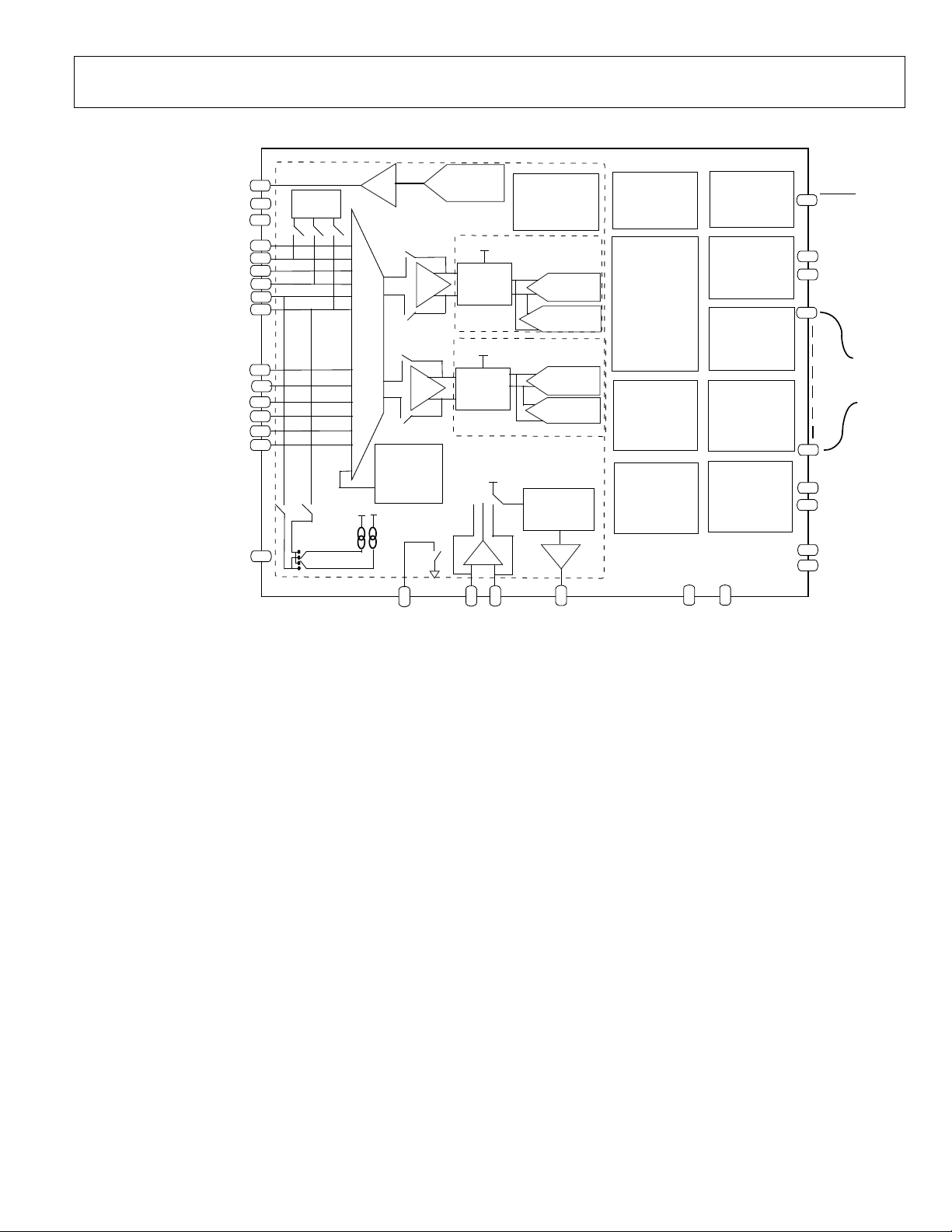
FUNCTIONAL BLOCK DIAGRAM
Figure 1. ADuCM360 Block Diagram
Rev. Pr R Page 2 of 21

Preliminary Technical Data
TABLE OF CONTENTS
Features ............................................................................................... 1
Functional Block Diagram ............................................................... 2
General Description .......................................................................... 4
Specifications ..................................................................................... 5
ADuCM360/ADuCM361 Microcontroller Electrical
Specifications ................................................................................. 5
ADuCM360/ADuCM361
Noise Resolution of Primary and Auxiliary ADCs ................ 10
I2C Timing Diagrams ................................................................. 12
SPI Timing Diagrams ................................................................. 13
Absolute Maximum Ratings .......................................................... 16
ESD Caution ................................................................................ 16
Outline Dimensions ........................................................................ 21
Rev. Pr R| Page 3 of 21

ADuCM360/ADuCM361
GENERAL DESCRIPTION
The ADuCM360 is a fully integrated, 4 kSPS, 24-bit data acquisition system incorporating dual, high performance multichannel sigma-delta (Σ-Δ) analog-to-digital converters (ADCs),
32-bit ARM Cortex M3® MCU, and Flash/EE memory on a
single chip. The part is designed for direct interfacing to
external precision sensors in both wired and battery powered
applications.
The ADuCM361 contains all the features of the ADuCM360
except the primary ADC, ADC0 is not available – only the
auxiliary ADC, ADC1 is available.
The device contains an on-chip 32 KHz oscillator and an
internal 16MHz high-frequency oscillator. This clock is routed
through a programmable clock divider from which the MCU
core clock operating frequency is generated. The maximum
core clock speed is 16MHz and this is not limited by operating
voltage or temperature.
The microcontroller core is a low power Cortex-M3 core from
ARM. It is a 32-bit RISC machine, offering up to 20 MIPS peak
performance. The Cortex-M3 MCU incorporates a flexible 11channel DMA controller supporting all wired (SPI, UART, I
communication peripherals. 128k Bytes of non-volatile
Flash/EE and 8k Bytes of SRAM are also integrated on-chip.
The Analog sub-system consists of dual ADCs each connected
to a flexible input MUX. Both ADCs can operate in fully
differential and single ended modes. Other on-chip ADC
features include dual programmable excitation current sources,
burn-out current sources and a bias voltage generator of
AVDD_REG/2 (900mV) to set the common-mode voltage of an
input channel. A low-side internal ground switch is provided to
allow powering down of a bridge between conversions. The
ADCs contain two parallel filters – a Sinc3 or Sinc4 in parallel
with a Sinc2. The Sinc3 or Sinc4 filter is for precision
measurements. The Sinc2 filter is for fast measurements and for
detection of step changes in the input signal The device also
contains a low noise, low drift internal band-gap reference or
can be configured to accept up to 2 external reference sources in
ratiometric measurement configurations. An option to buffer
the external reference inputs is also provided on-chip. A singlechannel buffered voltage output DAC is also provided on chip.
2
C)
Preliminary Technical Data
The ADuCM360/ADuCM361 also integrates a range of on-chip
peripherals which can be configured under microcontroller
software control as required in the application. These
peripherals include UART, I2C and dual SPI Serial I/O
communication controllers, 19-Pin GPIO Ports, 2 General
Purpose Timers, Wake-up Timer and System Watchdog Timer.
A 16-bit PWM with six output channels is also provided.
The ADuCM360/ADuCM361 is specifically designed to operate
in battery powered applications where low power operation is
critical. The microcontroller core can be configured in a normal
operating mode consuming 290μA/MHz (including
Flash/SRAM Idd) resulting in an overall system current
consumption of 1mA when all peripherals are active.
The part can also be configured in a number of low power
operating modes under direct program control, including
hibernate mode (internal wake-up timer active) consuming
only 4µA. In hibernate mode, peripherals such as external
interrupts or the internal wake up timer can wake up the device.
This allows the part to operate in an ultra-low power operating
mode and still respond to asynchronous external or periodic
events.
On-chip factory firmware supports in-circuit serial download
via a serial wire interface (2-pin JTAG system) and UART while
non-intrusive emulation is also supported via the serial wire
interface. These features are incorporated into a low-cost
QuickStart Development System supporting this Precision
Analog Microcontroller family.
The part operates from an external 1.8V to 3.6V voltage supply
and is specified over an industrial temperature range of -40°C to
125°C.
Rev. Pr R Page 4 of 21

Preliminary Technical Data
Conversion Rate1
Chop off
4 4000
Hz
RMS Noise and Data Output
See Noise and Resolution tables
ADuCM360/ADuCM361
SPECIFICATIONS
ADUCM360/ADUCM361 MICROCONTROLLER ELECTRICAL SPECIFICATIONS
AVDD/IOVDD = 1.8 V to 3.6V, Internal 1.2V reference, f
noted.
Table 1. ADuCM360/ADuCM361 Specifications
Parameter Test Conditions/Comments Min Typ Max Unit
ADC SPECIFICATIONS
Chop on 4 1333 Hz
Both Primary & Auxiliary
Channels
No Missing Codes1 Chop off (f
Chop on (f
≤ 500 Hz) 24 Bits
ADC
≤ 250 Hz) 24 Bits
ADC
= 16 MHz, all specifications TA = −40°C to +125°C, unless otherwise
CORE
Rates
Integral Nonlinearity1 Gain = 1
in the User Guide
Gain = 2, 4, 8, 16, 32, 64, 128
±15
±25
ppm of FSR
Offset Error
,2, 3
Chop off, offset error is in the
±100/Gain μV
order of the noise for the programmed gain and update rate
following calibration
Offset Error
Offset Error Drift vs.
Temperature
Offset Error Drift vs. Time
Full-Scale Error
Gain Drift vs. Temperature
1,2,3
Chop on ±1.0 μV
4
Chop off 100/ Gain nV/°C
Chop on 10 nV/°C
1,5, 6,7
±0.5/Gain TBD mV
TBD nV/1000
4
Gain = 1 to 16, external
±1 ppm/°C
reference
Gain = 32 to 128 external
±3
reference
Gain Error Drift vs. Time
TBD ppm/1000
PGA Gain Mismatch Error ±0.15 %
Power Supply Rejection
1,8
Chop on, ADC = 0.25 V (Gain =
85 dB
4), ext. reference
Chop off, ADC = 7.8 mV (Gain =
100 dB
128), ext. reference
Chop off, ADC = 1 V (Gain = 1),
85 dB
ext. reference
Absolute I nput Voltage Range
Unbuffered Mode Gain=1 AGND Avdd V
Buffered Mode Gain =1 AGND+ 100mV Avdd-100mV V
Unbuffered Mode:
Differential Input Voltage
1
Ranges
Gain >=2
Gain = 1
Gain = 2
Gain = 4
Gain = 8
Gain = 16
Gain = 32 (AVDD >=2.0V)
(AVDD <2.0V)
Gain = 64 (AVDD >=2.0V)
Rev. Pr R| Page 5 of 21
AGND
Avdd
±VREF
±500
±250
±125
±62.5
±26.56
±18.75
±13.28
ppm of FSR
hours
hours
mV
mV
mV
mV
mV
mV
mV
mV
mV

ADuCM360/ADuCM361
(AVDD <2.0V)
±9.375
mV
ADC Gain =2 to 128
80
dB
mode before measurement
Voltage TC
250 mV/°C
Internal V
1.2 V
Preliminary Technical Data
Parameter Test Conditions/Comments Min Typ Max Unit
Gain = 128 (AVDD >=2.0V)
(AVDD <2.0V)
Common mode Voltage, Vcm1 Vcm=(AIN(+)+AIN(-))/2,
AGND V
±6.64
±4.6875
Gain=2 to 128
Input current will be higher
when Vcm <0.5V
Input Current
1,9
Gain = 1, Buffered mode
1 nA
(excluding pins with Vbias)
Gain >1, Buffered mode
2 nA
(excluding pins with Vbias)
Unbuffered mode. Input current
500 nA/V
will vary with input voltage
Average Input Current Drift Buffered mode:
AIN0, AIN1, AIN2, AIN3
AIN4, AIN5, AIN6, AIN7
AIN8, AIN9, AIN10, AIN11
±5
±16
±9
Unbuffered mode ±250 pA/V/°C
Common-Mode Rejection DC1
On ADC Input ADC Gain =1 70 100
Common-Mode Rejection1
50 Hz/60 Hz
50 Hz/60 Hz ± 1 Hz,
16.7 Hz update rate, chop on
50 Hz update rate, chop off
ADC Gain =1 97 dB
ADC Gain =2 to 128 90 dB
Normal-Mode Rejection
1
50 Hz/60 Hz
On ADC Input 50 Hz/60 Hz ± 1 Hz, 16.6 Hz f
chop on, 50 Hz f
chop off
ADC/
60 80 dB
ADC/
TEMPERATURE SENSOR After user calibration
Voltage Output at 25°C MCU in power down or standby
82.1 mV
mV
mV
pA/°C
pA/°C
pA/°C
Accuracy 6 °C
GROUND SWITCH
Ron 12 Ohms
Allowable Current With 20K resistor off – direct
VOLTAGE REFERENCE
ADC Precision Reference
Initial Accuracy1 Measured at TA = 25°C -0.05 0.05 %
Reference Temperature
Coefficient (Tempco)
Power Supply Rejection1 100 dB
REF
20 mA
short to ground
1,8
−15 ±8 +15 ppm/°C
Rev. Pr R Page 6 of 21

Preliminary Technical Data
Normal Mode Rejection
80
Using external 150 kΩ reference
75 ppm/°C
Parameter Test Conditions/Comments Min Typ Max Unit
External Reference Input
Range
Input Current Buffered mode 15 nA
Unbuffered mode 500 nA/V
Buffered mode
Unbuffered mode
Minimum Differential voltage
between VREF+ and VREF- pins
is 400mV
0
0
ADuCM360/ADuCM361
AVDD-0.1
AVDD
V
V
Common Mode Rejection 78
Reference Detect Levels 400 mV
EXCITATION CURRENT SOURCES
Output Current Available from each current
source – 10/50/200uA nominal
Initial Tolerance at 25°C Iout >= 50uA ±5 %
Drift1 Using internal reference resistor 200 ppm/°C
resistor between IREF pin and
AGND. Resistor must have a drift
spec of 5ppm/°C
Initial Current Matching at 25°C1 Matching between both current
sources
Drift Matching1 50 ppm/°C
Load Regulation (AVDD) 1 AVDD = 3.3 V 0.2 %/V
Output Compliance1 10uA to 210uA Iout AGND − 30 mV AVDD − 0.85 V V
Iout >210uA AGND − 30 mV AVDD − 1.1 V V
DAC CHANNEL SPECIFICATIONS RL = 5 kΩ, CL = 100 pF
Voltage Range Internal reference 0 V
External reference 0 1.8 V
DC Specifications10
Resolution 12 Bits
Relative Accuracy ±3 LSB
Differential Nonlinearity Guaranteed monotonic ±0.5 ±1 LSB
Offset Error 1.2 V internal reference ±2 ±15 mV
Gain Error
NPN Mode
Resolution
Relative Accuracy
Differential Nonlinearity
Offset Error
Gain Error
Output Current Range
DAC AC CHARACTERISTICS
Voltage Output Settling Time 10 µs
Digital-to-Analog Glitch Energy 1 LSB change at major carry
1
V
range (reference = 1.2 V)
REF
(where maximum number of
bits simultaneously change in
the DAC0DAT register)
10 50 1000 μA
±0.5 %
12
0.008
±20 nV-sec
±1.0
±0.5
±0.35
±0.75
dB
REF
±1 %
23.6
V
Bits
LSB
LSB
mA
mA
mA
Rev. Pr R| Page 7 of 21

ADuCM360/ADuCM361
Logic 0 Input Current (leakage
V
= 0V
10
nA
VINH, Input High Voltage
0.7 x VDD
V
Oscillator
32,768
kHz
Preliminary Technical Data
Parameter Test Conditions/Comments Min Typ Max Unit
POWER-ON RESET (POR)
POR Trip Level Refers to voltage at DVDD pin
Power-on level 1.6 V
Power-down level 1.6 V
Timeout from POR 50 ms
WATCHDOG TIMER (WDT)
Timeout Period1 0.00003 8192 sec
Timeout Step Size T3CON[3:2]=[10] 7.8125 ms
FLASH/EE MEMORY1
Endurance11 20,000 Cycles
Data Retention12 Tj=85°C 10 Years
Digital Inputs All digital inputs
Logic 1 Input Current (leakage
current)
current)
V
=VDD or V
INH
= 1.8V
INH
Internal pull-up disabled
RESET
, SWCLK, SWDIO
INL
Internal pull-up disabled
RESET
, SWCLK, SWDIO
10
100
100
nA
Input Capacitance 10 pF
Logic Inputs
VINL, Input Low Voltage 0.2 x VDD V
μA
μA
Logic Outputs
VOH, Output High Voltage I
VOL, Output Low Voltage I
= 1mA VDD – 400mV V
SOURCE
= 1mA 0.4 V
SINK
CRYSTAL OSCILLATOR1
Logic Inputs, XTALI Only13
Input Low Voltage (VINL) 0.8 V
Input High Voltage (VINH) 1.7 V
XTALI Capacitance 6 pF
XTALO Capacitance 6 pF
ON-CHIP Low Power Oscillator
Accuracy −20 +20 %
ON-CHIP High Frequency
Oscillator
Oscillator 0.125 2 16 MHz
Accuracy To be confirmed across full
-1 1 %
temperature range of -40 to
+125C
MCU CLOCK RATE Eight programmable core clock
0.125 2 16 MHz
selections within this range:
Using an External Clock 0.032768 16 MHz
MCU START-UP TIME
At Power-On Includes kernel power-on
41 ms
execution time
After Reset Event Includes kernel power-on
1.44 ms
execution time
Rev. Pr R Page 8 of 21

Preliminary Technical Data
MCU clock rate = 500 KHz, Both
1
mA
Reduced temperature range
2 5
μA
ADuCM360/ADuCM361
Parameter Test Conditions/Comments Min Typ Max Unit
From MCU Power-Down
Fclk is the Cortex-M3 core clock 3-5 x Fclk
(mode 1, 2 and 3)
Fr om TOTAL-HALT or
30.8 μs
HIBERNATE (mode 4 or mode
5) mode
POWER REQUIREMENTS
Power Supply Voltages
VDD 1.8 3.6 V
Power Consumption
IDD (MCU Active Mode)
14,15
MCU clock rate = 16 MHz, all
5.5 mA
peripherals on
ADCs on (Input buffers off) with
PGAs Gain = 4, 1 x SPI on, all
timers on
IDD (MCU Powered Down)1 Full temperature range
4 10 μA
HIBERNATE (mode 5)
−40°C to +85°C
IDD (Primary ADC) (total)15 PGA enabled – total, G>=32 320 μA
PGA G=4/8/16 – PGA only 130 μA
G=32/64/128 – PGA only 180
Input Buffers 2 x Input buffers is 70uA 70 μA
Digital Interface +
Modulator
70
μA
IDD (Auxiliary ADC) Input buffers off, G=4/8/16 only 200 μA
External Reference Input
60uA each 120 μA
buffers
1
These numbers are not production tested but are guaranteed by design and/or characterization data at production release.
2
Tested at gain range = 4 after initial offset calibration.
3
Measured with an internal short. A system zero-scale calibration removes this error.
4
A recalibration at any temperature removes these errors.
5
These numbers do not include internal reference temperature drift.
6
Factory calibrated at gain = 1.
7
System calibration at a specific gain range removes the error at this gain range.
8
Measured using the box method.
9
Input current measured with one ADC measuring a channel. If both ADCs measure the same input channel, then the input current will increase – approximately
double
10
Reference DAC linearity is calculated using a reduced code range of 0x0AB to 0xF30.
11
Endurance is qualified to 20,000 cycles as per JEDEC Std. 22 Method A117 and measured at −40°C, +25°C, and +125°C. Typical endurance at 25°C is 170,000 cycles.
12
Retention lifetime equivalent at junction temperature (TJ) = 85°C as per JEDEC Std. 22 Method A117. Retention lifetime derates with junction temperature.
13
Voltage input levels only relevant if driving XTAL input from a voltage source. If a crystal is connected directly, the internal crystal interface will determine the
common mode voltage.
14
Typical additional supply current consumed during Flash/EE memory program and erase cycles is 7mA.
15
Total IDD for ADC includes figures for PGA≥32, input buffers, digital interface and the Sigma Delta modulator.
Rev. Pr R| Page 9 of 21

ADuCM360/ADuCM361
±1.0 V
±500 mV
±250 mV
±125 mV
±62.5 mV
±31.25 mV
±15.625 mV
±7.8125 mV
Chop Off
20.1
19.7
19.8
19.6
19.4
18.5
17.8
16.9
Preliminary Technical Data
NOISE RESOLUTION OF PRIMARY AND AUXILIARY ADCS
Table 2: RMS Noise (µV) vs. Gain and Output Update Rate
(Using an Internal Reference (1.2V) Both ADCs)
Update Rate (Hz) Gain of 1 Gain of 2 Gain of 4 Gain of 8 Gain of 16 Gain of 32 Gain of 64 Gain of 128
3.75 (Chop On)
ADCxFLT = 0x8D7C
30 (Chop Off)
ADCxFLT = 0x007E
50 (Chop Off)
ADCxFLT = 0x007D
100 (Chop Off)
ADCxFLT = 0x004D
488 (Chop Off Sinc4)
ADCxFLT = 0x100F
976 (Chop Off Sinc4)
ADCxFLT = 0x1007
1953 (Chop Off Sinc4)
ADCxFLT = 0x1003
3906 (Chop Off Sinc4)
ADCxFLT = 0x1001
1.05 0.45 0.23 0.135 0.072 0.064 0.055 0.052
2.1 1.37 0.63 0.37 0.22 0.2 0.16 0.155
3.7 1.6 0.83 0.47 0.29 0.24 0.21 0.2
5.45 2.41 1.13 0.63 0.38 0.32 0.27 0.25
10 4.7 2.2 1.3 0.79 0.67 0.58 0.57
13.5 6.5 3.3 1.7 1.1 0.91 0.74 0.7
19.3 10 4.7 2.6 1.55 1.3 1.15 1.0
67.0 36 16.6 8.8 4.9 2.68 1.76 1.4
Table 3: Typical Output RMS Effective Number of Bits in Normal Mode
(Using an Internal Reference (1.2V), Both ADCs, Peak-to-Peak Bits in Parentheses)
ADC
Register
Status
Chop On
Sinc3
Sinc3
Chop Off
Sinc3
Chop Off
Sinc3
Chop Off
Sinc4
Chop Off
Sinc4
Chop Off
Sinc4
Chop Off
Sinc4
Data
Update
Rate
3.75 Hz
30 Hz
50 Hz
100 Hz
488 Hz
976 Hz
1953
Hz
3906
Hz
Input Voltage Noise (mV)
(PGA = 1)
21.1
(18.4p-p)
(17.4p-p)
19.3
(16.6p-p)
18.7
(16p-p)
17.9
(15.2p-p)
17.4
(14.7p-p)
16.9
(14.2p-p)
15.1
(12.4p-p)
(PGA = 2)
21.3
(18.6p-p)
(17p-p)
19.5
(16.8p-p)
18.9
(16.2p-p)
18
(15.2p-p)
17.5
(14.8p-p)
16.9
(14.2p-p)
15
(12.3p-p)
(PGA = 4)
21.3
(18.6p-p)
(17.1p-p)
19.5
(16.8p-p)
19
(16.3p-p)
18.1
(15.3p-p)
17.5
(14.8p-p)
17
(14.3p-p)
15.1
(12.4p-p)
(PGA = 8)
21.1
(18.4p-p)
(16.9p-p)
19.3
(16.6p-p)
18.9
(16.2p-p)
17.8
(15.1p-p)
17.4
(14.7p-p)
16.8
(14p-p)
15.1
(12.4p-p)
(PGA = 16)
21
(18.3p-p)
(16.7p-p)
19
(16.3p-p)
18.6
(16.1p-p)
17.5
(14.8p-p)
17.1
(14.3p-p)
16.6
(13.8p-p)
14.9
(12.2p-p)
(PGA = 32)
20.2
(17.4p-p)
(15.8p-p)
18.3
(15.5p-p)
17.8
(15.1p-p)
16.8
(14p-p)
16.3
(13.6p-p)
15.8
(13.1p-p)
14.8
(12p-p)
(PGA = 64)
19.4
(16.7p-p)
(15.1p-p)
17.4
(14.7p-p)
17.1
(14.4p-p)
16
(13.3p-p)
15.6
(12.9p-p)
15
(13.1p-p)
14.4
(11.7p-p)
(PGA = 128)
18.5
(15.7p-p)
(14.2p-p)
16.5
(13.8p-p)
16.2
(13.5p-p)
15
(12.3p-p)
14.7
(12p-p)
14.2
(11.5p-p)
13.7
(11p-p)
Rev. Pr R Page 10 of 21

Preliminary Technical Data
100 (Chop Off)
ADuCM360/ADuCM361
Table 4: RMS Noise (µV) vs. Gain and Output Update Rate
(Using an External Reference (2.5V) Both ADCs)
Update Rate (Hz) Gain of 1 Gain of 2 Gain of 4 Gain of 8 Gain of 16 Gain of 32 Gain of 64 Gain of 128
4.55 (Chop On)
ADCxFLT = 0x88FD
30 (Chop Off)
ADCxFLT = 0x007E
50 (Chop Off)
ADCxFLT = 0x007D
1.1 0.5 0.27 0.17 0.088 0.07 0.06 0.58
3 1.4 0.85 0.44 0.27 0.22 0.19 0.17
3.9 2.2 0.92 0.46 0.3 0.21 0.2 0.19
ADCxFLT = 0x004F
488 (Chop Off Sinc4)
ADCxFLT = 0x100F
976 (Chop Off Sinc4)
ADCxFLT = 0x1007
1953 (Chop Off Sinc4)
ADCxFLT = 0x1003
3906 (Chop Off Sinc4)
ADCxFLT = 0x1001
5.2 2.8 1.25 0.63 0.38 0.32 0.28 0.26
9.3 5.0 2.5 1.2 0.75 0.7 0.57 0.5
12.5 7 3.5 1.75 1.2 0.83 0.77 0.75
20.0 10 5.7 2.6 1.71 1.3 1.24 1.1
140.0 70.0 35.0 17.2 8.9 4.8 2.65 1.88
Table 5: Typical Output RMS Effective Number of Bits in Normal Mode
(Using an External Reference (2.5V), Both ADCs, Peak-to-Peak Bits in Parentheses)
ADC
Register
Status
Chop On
Sinc3
Chop Off
Sinc3
Chop Off
Sinc3
Chop Off
Sinc3
Chop Off
Sinc4
Chop Off
Sinc4
Chop Off
Sinc4
Chop Off
Sinc4
Data
Update
Rate
3.75 Hz
30 Hz
50 Hz
100 Hz
488 Hz
976 Hz
1953
Hz
3906
Hz
Input Voltage Noise (mV)
±1.0 V
(PGA = 1)
22.1
(19.4p-p)
20.7
(18p-p)
20.3
(17.6p-p)
19.9
(17.2p-p)
19
(16.3p-p)
18.6
(15.9p-p)
17.9
(15.2p-p)
15.1
(12.4p-p)
±500 mV
(PGA = 2)
22.3
(19.5p-p)
20.7
(18p-p)
20.1
(17.4p-p)
19.8
(17p-p)
18.9
(16.2p-p)
18.4
(15.7p-p)
17.9
(15.2p-p)
15.1
(12.4p-p)
±250 mV
(PGA = 4)
22.1
(19.4p-p)
20.5
(17.7p-p)
20.4
(17.7p-p)
19.9
(17.2p-p)
18.9
(16.2p-p)
18.4
(15.7p-p)
17.7
(15p-p)
15.1
(12.4p-p)
±125 mV
(PGA = 8)
21.8
(19.1p-p)
20.5
(17.7p-p)
20.4
(17.7p-p)
19.9
(17.2p-p)
19
(16.3p-p)
18.4
(15.7p-p)
17.9
(15.2p-p)
15.1
(12.4p-p)
±62.5 mV
(PGA = 16)
21.8
(19.1p-p)
20.1
(17.4p-p)
20
(17.3p-p)
19.6
(16.9p-p)
18.7
(15.9p-p)
18
(15.3p-p)
17.5
(14.8p-p)
15.1
(12.4p-p)
±31.25 mV
(PGA = 32)
21.1
(18.4p-p)
19.4
(16.7p-p)
19.5
(16.8p-p)
18.9
(16.2p-p)
17.8
(15p-p)
17.5
(14.8p-p)
16.9
(14.2p-p)
15
(12.3p-p)
±15.625 mV
(PGA = 64)
20.3
(17.6p-p)
18.6
(15.9p-p)
18.6
(15.9p-p)
18.1
(15.4p-p)
17.1
(14.3p-p)
16.6
(13.9p-p)
15.9
(13.2p-p)
14.8
(12.1p-p)
±7.8125 mV
(PGA = 128)
19.4
(16.6p-p)
17.8
(15.1p-p)
17.6
(14.9p-p)
17.2
(14.5p-p)
16.3
(13.5p-p)
15.7
(12.9p-p)
15.1
(12.4p-p)
14.3
(11.6p-p)
Rev. Pr R| Page 11 of 21

ADuCM360/ADuCM361
Parameter
Description
Min
Max
Unit
t
Bus-free time between a stop condition and a start condition
1.3
-
µ
tL
SCL low pulse width
4.7 - μs
04955-054_edited
SDA (I/O)
t
BUF
MSB LSB ACK MSB
1982–71
SCL (I)
P S
STOP
CONDITION
START
CONDITION
S(R)
REPEATED
START
t
SUP
t
R
t
F
t
F
t
R
t
H
t
L
t
SUP
t
DSU
t
DHD
t
RSU
t
DHD
t
DSU
t
SHD
t
PSU
Preliminary Technical Data
I2C TIMING DIAGRAMS
Capacitive load for each of the I2C1-bus line, Cb = 400pF maximum as per I2C-bus specifications.
2
C timing is guaranteed by design and not production tested.
I
2
Table 6. I
tL Serial Clock (SCL) low pulse width 1300 - ns
tH SCL high pulse width 600 - ns
t
SHD
t
DSU
t
DHD
t
RSU
t
PSU
BUF
tR Rise time for both SCL and serial data (SDA) 20 + 0.1 Cb 300 ns
tF Fall time for both SCL and SDA 20 + 0.1 Cb 300 ns
t
SUP
Table 7. I
Parameter Description Min Max Unit
C Timing in Fast Mode (400 kHz)
Start condition hold time 600 - ns
Data setup time 100 - ns
Data hold time 0 - ns
Setup time for repeated start 600 - ns
Stop condition setup time 600 - ns
Pulse width of spike suppressed 0 50 ns
2
C Timing in Standard Mode (100 kHz)
s
tH SCL high pulse width 4.0 - ns
t
Start condition hold time 4.7 - μs
SHD
t
Data setup time 250 - ns
DSU
t
Data hold time 0 - μs
DHD
t
Setup time for repeated start 4.0 - μs
RSU
t
Stop condition setup time 4.0 - μs
PSU
t
Bus-free time between a stop condition and a start condition 4.7 - μs
BUF
tR Rise time for both SCL and SDA - 1 μs
tF Fall time for both SCL and SDA - 300 ns
2
Figure 2. I
1
2
I
C refers to a communications protocol originally developed by Philips Semiconductors (now NXP Semiconductors).
C Compatible Interface Timing
Rev. Pr R Page 12 of 21

Preliminary Technical Data
04955-055_edited
SCLK
(POLARITY = 0)
SCLK
(POLARITY = 1)
MOSI MSB BITS 6 TO 1 LSB
MISO MSB IN BITS 6 TO 1 LSB IN
t
SH
t
SL
t
SR
t
SF
t
DR
t
DF
t
DAV
t
DSU
t
DHD
ADuCM360/ADuCM361
SPI TIMING DIAGRAMS
Table 8. SPI Master Mode Timing
Parameter Description Min Typ Max Unit
tSL SCLK low pulse width1 (SPIDIV + 1) × t
tSH SCLK high pulse width1 (SPIDIV + 1) × t
t
Data output valid after SCLK edge 0 35.5 ns
DAV
t
Data output setup before SCLK edge1 (SPIDIV + 1) ×
DOSU
t
Data input setup time before SCLK edge 58.7 ns
DSU
t
Data input hold time after SCLK edge 16 ns
DHD
t
UCLK
ns
tDF Data output fall time 12 35.5 ns
tDR Data output rise time 12 35.5 ns
tSR SCLK rise time 12 35.5 ns
tSF SCLK fall time 12 35.5 ns
1
t
= 62.5 ns. It corresponds to the internal 16MHz clock before the clock divider.
UCLK
ns
UCLK
ns
UCLK
Figure 3. SPI Master Mode Timing (PHASE Mode = 1)
Rev. Pr R| Page 13 of 21

ADuCM360/ADuCM361
t
Data output valid after CS edge
25
ns
04955-056_edited
SCLK
(POLARITY = 0)
SCLK
(POLARITY = 1)
t
SH
t
SL
t
SR
t
SF
MOSI MSB BITS 6 TO 1 LSB
MISO MSB IN BITS 6 TO 1 LSB IN
t
DR
t
DF
t
DAV
t
DOSU
t
DSU
t
DHD
Preliminary Technical Data
Figure 4. SPI Master Mode Timing (PHASE Mode = 0)
Table 9. SPI Slave Mode Timing
Parameter Description Min Typ Max Unit
tCS
tSL SCLK low pulse width1 (SPIDIV + 1) × t
tSH SCLK high pulse width1 62.5 (SPIDIV + 1) × t
t
Data output valid after SCLK edge 49.1 ns
DAV
t
Data input setup time before SCLK edge 20.2 ns
DSU
t
Data input hold time after SCLK edge 10.1 ns
DHD
to SCLK edge 38 ns
CS
ns
UCLK
ns
UCLK
tDF Data output fall time 12 35.5 ns
tDR Data output rise time 12 35.5 ns
tSR SCLK rise time 12 35.5 ns
tSF SCLK fall time 12 35.5 ns
DOCS
t
SFS
high after SCLK edge 0 ns
CS
1
t
= 62.5 ns. It corresponds to the internal 16MHz clock before the clock divider.
UCLK
Rev. Pr R Page 14 of 21

Preliminary Technical Data
04955-057_edited
SCLK
(POLARITY = 0)
CS
SCLK
(POLARITY = 1)
t
SH
t
SL
t
SR
t
SF
t
SFS
MISO MSB BITS 6 TO 1 LSB
MOSI MSB IN BITS 6 TO 1 LSB IN
t
DHD
t
DSU
t
DAV
t
DR
t
DF
t
CS
04955-058_edited
SCLK
(POLARITY = 0)
CS
SCLK_
(POLARITY = 1)
t
SH
t
SL
t
SR
t
SF
t
SFS
MISO
MOSI
MSB IN BITS 6 TO 1 LSB IN
t
DHD
t
DSU
MSB BITS 6 TO 1 LSB
t
DOCS
t
DAV
t
DR
t
DF
t
CS
ADuCM360/ADuCM361
Figure 5. SPI Slave Mode Timing (PHASE Mode = 1)
Figure 6. SPI Slave Mode Timing (PHASE Mode = 0)
Rev. Pr R| Page 15 of 21

ADuCM360/ADuCM361
Digital Input Voltage to DGND
−0.3 V to 3.96V
Peak Solder Reflow Temperature
Preliminary Technical Data
ABSOLUTE MAXIMUM RATINGS
Table 10.
Parameter Rating
AVDD/IOVDD to GND −0.3 V to 3.96V
Digital Output Voltage to DGND −0.3 V to 3.96V
V
to AGND −0.3 V to TBD
REF
Analog Inputs to AGND −0.3 V to TBD
Operating Temperature Range –40°C to +125°C
Storage Temperature Range –65°C to +150°C
Junction Temperature 150°C
ESD (Human Body Model) rating
All Pins
θJA Thermal Impedance
48-Pin LFCSP _VQ 27°C/W
SnPb Assemblies (10 sec to 30 sec) 240°C
Pb-Free Assemblies
(20 sec to 40 sec)
Stresses above those listed under Absolute Maximum Ratings may cause permanent damage to the device. This is a stress rating only;
functional operation of the device at these or any other conditions above those indicated in the operational section of this specification is
not implied. Exposure to absolute maximum rating conditions for extended periods may affect device reliability.
±2kV
260°C
ESD CAUTION
Rev. Pr R Page 16 of 21

Preliminary Technical Data
Pin Configuration and Function Descriptions
ADuCM360/ADuCM361
Figure 7. ADuCM360/ADuCM361 Pinout
Table 11. Pin Function Descriptions
Pin No. Mnemonic Description
1
2 P2.1/SDA/UARTDCD General-Purpose Input and General-Purpose Output P2.1/ I2C serial data Pin/Alternatively, this
3 P2.2/BM General-Purpose Input and General Purpose Output P2.2/ Boot mode input select pin. When
4 XTAL0 External Crystal Oscillator Output Pin. Optional 32.768kHz source for Real time clock.
5 XTAL1 External Crystal Oscillator Input Pin. Optional 32.768kHz source for Real time clock.
6 IOVDD Digital System Supply pin.
7 DVDD_REG Internal Digital Regulator Supply Output. This pin must be connected to ground via a 470nF
8 AIN0 ADC Analog Input 0. This pin can be configured as a positive or negative input to either ADC in
9 AIN1 ADC Analog Input 1. This pin can be configured as a positive or negative input to either ADC in
10 AIN2 ADC Analog Input 2. This pin can be configured as a positive or negative input to either ADC in
RESET
Reset. Input pin, active low. An internal pull-up is provided.
pin may be the UART Data carrier Detect pin.
This is a multi function input/output pin.
this pin is held low during any reset sequence, the part will enter UART download mode.
This is a dual function input/output pin.
capacitor.
Note: This pin must be connected to pin 18, AVDD_REG
Differential or single ended modes.
Differential or single ended modes.
Rev. Pr R| Page 17 of 21

ADuCM360/ADuCM361
Differential or single ended modes.
17
AVDD
Analog System Supply pin.
Pin No. Mnemonic Description
11 AIN3 ADC Analog Input 3. This pin can be configured as a positive or negative input to either ADC in
Differential or single ended modes.
12 AIN4/IEXC ADC Analog Input 4. This pin can be configured as a positive or negative input to either ADC in
Differential or single ended modes.
Or, it may be configured as the output pin for either Excitation current source 0 or 1.
13 GND_SW Sensor Power Switch to Analog Ground Reference.
14 VREF+ External Reference Positive Input, an external reference can be applied between VREF+ and
VREF-.
15 VREF− External Reference Negative Input, an external reference can be applied between VREF+ and
VREF-.
16 AGND Analog System Ground reference pin.
18 AVDD_REG Internal Analog Regulator Supply Output. This pin must be connected to ground via a 470nF
capacitor.
Note: This pin must be connected to pin 7, DVDD_REG
19 DAC DAC Voltage Output
20 INT_REF This pin must be connected to ground via a 470nF decoupling capacitor.
21 IREF Optional reference current resistor connection for the Excitation current sources.
Reference current set by low drift external resistor (5ppm/C).
22 AIN5/IEXC Multi-Function Pin: ADC Analog Input 5. This pin can be configured as a positive or negative input
to either ADC in Differential or single ended modes. Alternatively, it may be configured as the
output pin for either Excitation current source 0 or 1. Or, it may be configured as the output pin for
either Excitation current source 0 or 1.
23 AIN6/IEXC Multi-Function Pin: ADC Analog Input 6. This pin can be configured as a positive or negative input
to either ADC in Differential or single ended modes.
Or, it may be configured as the output pin for either Excitation current source 0 or 1.
24 AIN7/VBIAS0/IEXC/EXT_REF2IN+ Multi-Function Pin: ADC Analog Input 7. This pin can be configured as a positive or negative input
to either ADC in differential or single ended modes. Alternatively, this pin can be configured as an
analog output pin to generate a Bias Voltage, VBIAS3 of AVDD_REG/2.
Or, it may be configured as the output pin for either Excitation current source 0 or 1. Alternatively,
this pin can be configured as an external reference 2 positive input.
25 AIN8/EXT_REF2IN- Multi-Function Pin: ADC Analog Input 8. This pin can be configured as a positive or negative input
to either ADC in Differential or single ended modes. Alternatively, this pin can be configured as an
external reference 2 negative input.
26 AIN9 ADC Analog Input 9. This pin can be configured as a positive or negative input to either ADC in
Differential or single ended modes. Alternatively, this pin can be configured as the non-inverting
input to the DAC output buffer when the DAC is configured for NPN mode.
27 AIN10 ADC Analog Input 10. This pin can be configured as a positive or negative input to either ADC in
Differential or single ended modes.
28 AIN11/VBIAS1 Multi-Function Pin: ADC Analog Input 11. This pin can be configured as a positive or negative input
to either ADC in Differential or single ended modes. Alternatively, this pin can be configured as an
analog output pin to generate a Bias Voltage, VBIAS5 of AVdd/2.
29 P0.0/MISO1 General-Purpose Input and General-Purpose Output P0.0/SPI1 Master In – Slave out Pin.
This is a dual function input/output pin.
30 P0.1/SCLK1/SCL/SIN General-Purpose Input and General-Purpose Output P0.1/SPI1 Serial Clock Pin/I2C Serial Clock
Pin/ UART Serial Input. This is a multi function input/output pin.
This pin will be the data input for the UART downloader.
31 P0.2/MOSI1/SDA/SOUT General-Purpose Input and General-Purpose Output P0.2/ SPI1 Master Out – Slave In Pin /I2C
Serial Data Pin/ UART Serial output. This is a multi function input/output pin.
This pin will be the data output for the UART downloader.
32
33 P0.4/RTS/ECLKO General-Purpose Input and General-Purpose Output P0.4/ Request-to-Send Signal in UART
34 P0.5/CTS/IRQ1 General-Purpose Input and General-Purpose Output P0.5/ Clear-to-Send Signal in UART Mode. /
P0.3/IRQ0/
CS1
General-Purpose Input and General-Purpose Output P0.3/ External Interrupt Request 0/ SPI1
Chip Select Pin (Active Low). This is a triple function input/output pin.
Mode/ Clock out (for test purposes) pin. This is a triple function input/output pin.
External Interrupt Request 1.
Rev. Pr R Page 18 of 21
Preliminary Technical Data

Preliminary Technical Data
This is a dual function input/output pin.
35
P0.6/IRQ2/SIN
General-Purpose Input and General-Purpose Output P0.6/ External Interrupt Request 2/ UART
43
P1.5/IRQ5/PWM3/SCLK0
General-Purpose Input and General-Purpose Output P1.5/ External Interrupt Request 5/ PWM3
47
SWCLK
Serial Wire debug clock input pin.
Pin No. Mnemonic Description
Serial Input. This is a triple function input/output pin.
36 P0.7/POR/SOUT General-Purpose Input and General-Purpose Output P0.7/ Power on Reset active high bit/ UART
Serial output. This is a triple function input/output pin.
37 IOVDD Digital System Supply pin.
38 P1.0/IRQ3/PWMSYNC/ECLKI General-Purpose Input and General Purpose Output P1.0/ External Interrupt Request 3/ PWM
external Sync input/External clock input pin.
This is a Quad function input/output pin.
39 P1.1/IRQ4/PWMTRIP/DTR General-Purpose Input and General Purpose Output P1.1/ External Interrupt Request 4/ PWM
external trip input/UART Data terminal Ready pin.
This is a multi function input/output pin.
40 P1.2/PWM0/RI General-Purpose Input and General-Purpose Output P1.2/PWM0 Output/UART Ring Indicator
pin.
This is a triple function input/output pin.
41 P1.3/PWM1/DSR General-Purpose Input and General-Purpose Output P1.3/PWM1 Output/UARTData Set Ready
pin.
This is a triple function input/output pin.
42 P1.4/PWM2/MISO0 General-Purpose Input and General-Purpose Output P1.4/PWM2 Output/ SPI0 Master In –
Slave out Pin.
This is a triple function input/output pin.
ADuCM360/ADuCM361
Output/ SPI0 Serial Clock Pin.
This is a Quad function input/output pin.
44 P1.6/IRQ6/PWM4/MOSI0 General-Purpose Input and General-Purpose Output P1.6/ External Interrupt Request 6/ PWM4
Output/ SPI0 Master out, Slave in Pin.
This is a Quad function input/output pin.
45
46 P2.0/SCL/UARTCLK General-Purpose Input and General Purpose Output P2.0/ I2C Serial Clock Pin. Alternatively,
48 SWDIO Serial Wire debug data input/output pin.
EP **Exposed Paddle. The LFCSP_VQ has an exposed paddle that MUST BE connected to digital
P1.7/IRQ7/PWM5/
CS0
General-Purpose Input and General-Purpose Output P1.7/ External Interrupt Request 7/ PWM5
Output/ SPI0 Chip Select Pin (Active Low).
This is a Quad function input/output pin.
this pin may be an optional input clock pin for the UART block only.
This is a Triple function input/output pin.
ground.
Rev. Pr R| Page 19 of 21

ADuCM360/ADuCM361
-40
-20020406080100
120
TYPICAL PERFORMANCE CHARACTERISTICS
Figure 8. Common Mode Voltage (Vcm) in Volts vs Input Current in nA, Gain=4, ADC input 250mV, AVdd=3.6V, T=25C
Preliminary Technical Data
Figure 9. Common Mode Voltage (Vcm) in Volts vs Input Current in nA, Gain=128, ADC input 7.8125mV, AVdd=3.6V, T=25C
14000000
12000000
10000000
ADC Codes
8000000
6000000
4000000
2000000
0
Temp
Figure 10. ADC Codes (decimal values) v Die temperature
Rev. Pr R Page 20 of 21

Preliminary Technical Data
©2012 Analog Devices, Inc. All rights reserved. Trademarks
112408-B
FOR PRO P E R CONNECTIO N OF
THE EXPOSED PAD, REFER TO
THE PIN CONFIGURATION AND
FUNCTION DESCRIPT IONS
SECTION OF THIS DATA SHEET.
COMPLIANT TO JE DE C S TANDARDS MO-220-WKKD.
1
0.50
BSC
BOTTOM VIEW
TOP VIEW
PIN 1
INDICATOR
7.00
BSC SQ
48
13
24
25
36
37
12
EXPOSED
PAD
PIN 1
INDICATOR
5.20
5.10 SQ
5.00
0.45
0.40
0.35
SEATING
PLANE
0.80
0.75
0.70
0.05 MAX
0.02 NOM
0.25 MIN
0.20 REF
COPLANARITY
0.08
0.30
0.23
0.18
OUTLINE DIMENSIONS
ADuCM360/ADuCM361
(CP-48-4)
Figure 11. 48-Lead Lead Frame Chip Scale Package [LFCSP_VQ]
7 mm × 7 mm Body, Very Thin Quad
Dimensions shown in millimeters
and registered trademarks are the property of their
respective owners. PR09743-0-5/12(PrR).
Rev. Pr R| Page 21 of 21
 Loading...