Analog Devices ADuC845 7 8 b Datasheet
MicroConverter® Multichannel
24-/16-Bit ADCs with Embedded 62 kB
Flash and Single-Cycle MCU
FEATURES
High resolution Σ-∆ ADCs
2 independent 24-bit ADCs on the ADuC845
Single 24-bit ADC on the ADuC847 and
single 16-bit ADC on the ADuC848
Up to 10 ADC input channels on all parts
24-bit no missing codes
22-bit rms (19.5 bit p-p) effective resolution
Offset drift 10 nV/°C, gain drift 0.5 ppm/°C chop enabled
Memory
62-kbyte on-chip Flash/EE program memory
4-kbyte on-chip Flash/EE data memory
Flash/EE, 100-year retention, 100 kcycle endurance
3 levels of Flash/EE program memory security
In-circuit serial download (no external hardware)
High speed user download (5 sec)
2304 bytes on-chip data RAM
8051-based core
8051-compatible instruction set
High performance single-cycle core
32 kHz external crystal
On-chip programmable PLL (12.58 MHz max)
3 × 16-bit timer/counter
24 programmable I/O lines, plus 8 analog or
digital input lines
11 interrupt sources, two priority levels
Dual data pointer, extended 11-bit stack pointer
On-chip peripherals
Internal power-on reset circuit
12-bit voltage output DAC
Dual 16-bit Σ-∆ DACs
On-chip temperature sensor (ADuC845 only)
Dual excitation current sources (200 µA)
Time interval counter (wake-up/RTC timer)
UART, SPI®, and I
High speed dedicated baud rate generator (incl. 115,200)
Watchdog timer (WDT)
Power supply monitor (PSM)
2
C® serial I/O
ADuC845/ADuC847/ADuC848
Power
Normal: 4.8 mA max @ 3.6 V (core CLK = 1.57 MHz)
Power-down: 20 µA max with wake-up timer running
Specified for 3 V and 5 V operation
Package and temperature range:
52-lead MQFP (14 mm × 14 mm), −40°C to +125°C
56-lead LFCSP (8 mm × 8 mm), −40°C to +85°C
APPLICATIONS
Multichannel sensor monitoring
Industrial/environmental instrumentation
Weigh scales, pressure sensors, temperature monitoring
Portable instrumentation, battery-powered systems
Data logging, precision system monitoring
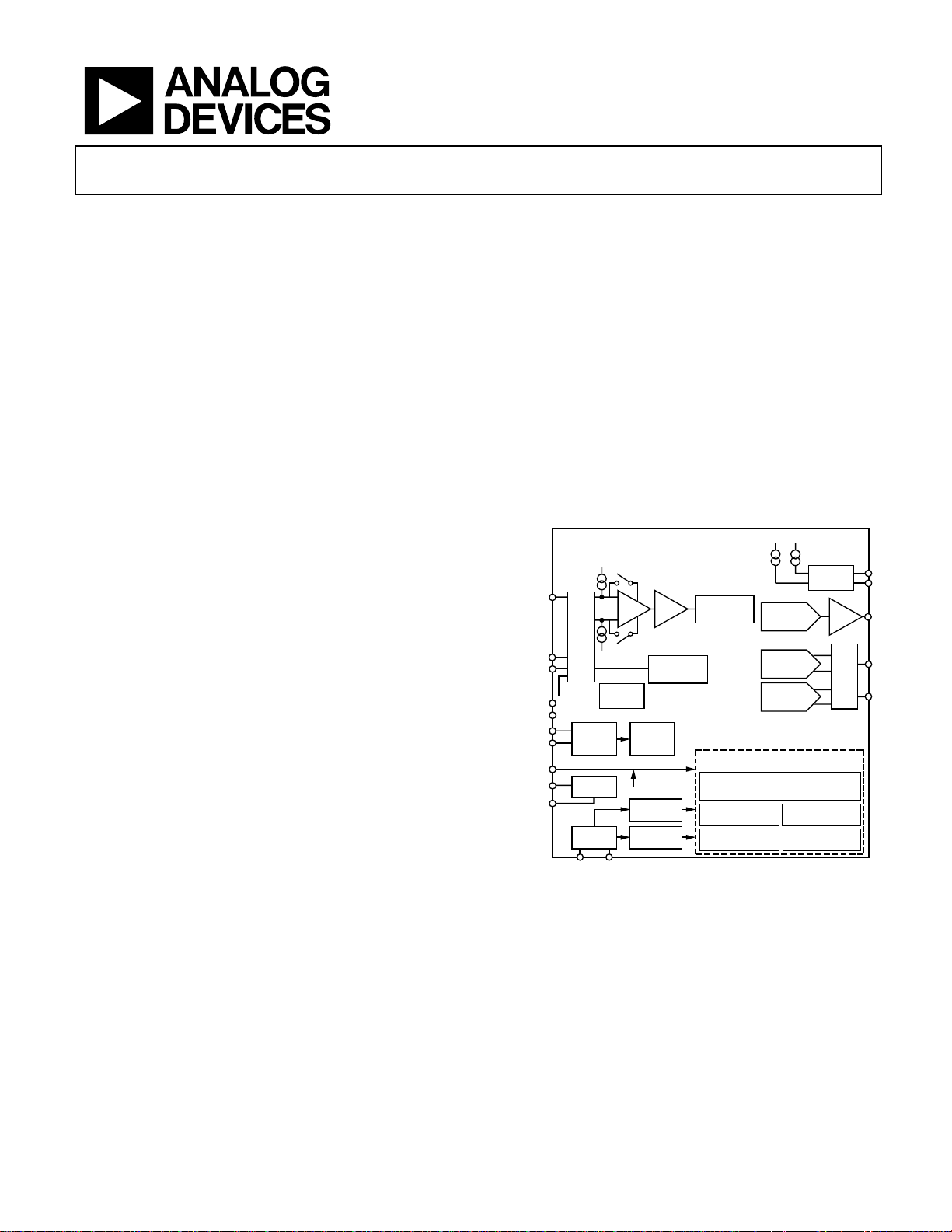
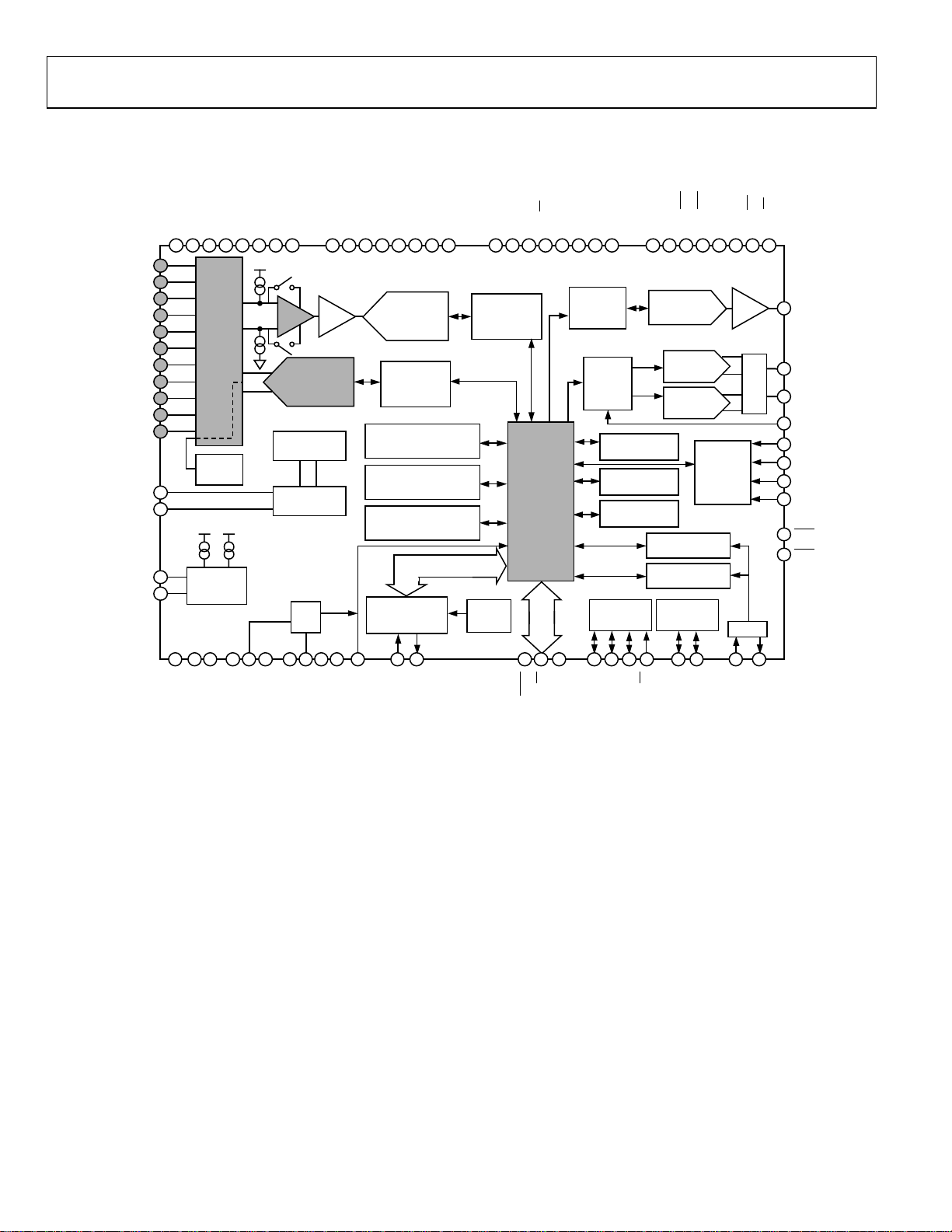
FUNCTIONAL BLOCK DIAGRAM
AV
DD
12-BIT
DAC
DUAL 16-BIT
Σ-∆ DAC
DUAL 16-BIT
PWM
POWER SUPPLY MON
WATCHDOG TIMER
UART, SPI, AND I
SERIAL I/O
CURRENT
SOURCE
BUF
MUX
2
C
AIN1
AIN10
AINCOM
REFIN2+
REFIN2–
REFIN–
REFIN+
RESET
DV
DGND
ADuC845
AVCO
PGABUF
MUX
AGND
TEMP
SENSOR
EXTERNAL
V
REF
DETECT
DD
POR
OSC
XTAL2XTAL1
AUXILIARY
24-BIT Σ-∆ ADC
INTERNAL
BAND GAP
V
REF
PLL AND PRG
CLOCK DIV
WAKE-UP/
RTC TIMER
PRIMARY
24-BIT Σ-∆ ADC
SINGLE-CYCLE 8061-BASED MCU
62 kBYTES FLASH/EE PROGRAM MEMORY
4 kBYTES FLASH/EE DATA MEMORY
2304 BYTES USER RAM
3 × 16 BIT TIMERS
BAUD RATE TIMER
4 × PARALLEL
PORTS
Figure 1. ADuC845 Functional Block Diagram
IEXC1
IEXC2
DAC
PWM0
PWM1
04741-001
Rev. B
Information furnished by Analog Devices is believed to be accurate and reliable.
However, no responsibility is assumed by Analog Devices for its use, nor for any
infringements of patents or other rights of third parties that may result from its use.
Specifications subject to change without notice. No license is granted by implication
or otherwise under any patent or patent rights of Analog Devices. Trademarks and
registered trademarks are the property of their respective owners.
One Technology Way, P.O. Box 9106, Norwood, MA 02062-9106, U.S.A.
Tel: 781.329.4700
Fax: 781.326.8703 © 2005 Analog Devices, Inc. All rights reserved.
www.analog.com

ADuC845/ADuC847/ADuC848
TABLE OF CONTENTS
Specifications..................................................................................... 4
ADC SFR Interface..................................................................... 39
Abosolute Maximum Ratings ....................................................... 10
ESD Caution................................................................................ 10
Pin Configurations and Function Descriptions .........................11
General Description ....................................................................... 15
8052 Instruction Set ...................................................................18
Timer Operation......................................................................... 18
ALE............................................................................................... 18
External Memory Access........................................................... 18
Complete SFR Map .................................................................... 19
Functional Description .................................................................. 20
8051 Instruction Set ...................................................................20
Memory Organization ............................................................... 22
Special Function Registers (SFRs)............................................ 24
ADC Circuit Information.......................................................... 26
Auxiliary ADC (ADuC845 Only) ............................................32
Reference Inputs......................................................................... 32
Burnout Current Sources ..........................................................32
Reference Detect Circuit ........................................................... 33
Sinc Filter Register (SF) .............................................................33
Σ-∆ Modulator ............................................................................ 33
Digital Filter ................................................................................33
ADC Chopping........................................................................... 34
Calibration................................................................................... 34
Programmable Gain Amplifier................................................. 35
Bipolar/Unipolar Configuration ..............................................35
Data Output Coding ..................................................................36
Excitation Currents ....................................................................36
ADC Power-On .......................................................................... 36
Typical Performance Characteristics........................................... 37
Functional Description .................................................................. 39
ADCSTAT (ADC Status Register) ........................................... 40
ADCMODE (ADC Mode Register)......................................... 41
ADC0CON1 (Primary ADC Control Register)..................... 43
ADC0CON2 (Primary ADC Channel Select Register) ........ 44
ADC1CON (Auxiliary ADC Control Register) (ADuC845
............................................................................................ 45
Only)
SF (ADC Sinc Filter Control Register) .................................... 46
ICON (Excitation Current Sources Control Register) .......... 47
Nonvolatile Flash/EE Memory Overview ............................... 48
Flash/EE Program Memory...................................................... 49
User Download Mode (ULOAD)............................................. 50
Using Flash/EE Data Memory .................................................. 51
Flash/EE Memory Timing ........................................................ 52
DAC Circuit Information .......................................................... 53
Pulse-Width Modulator (PWM).............................................. 55
On-Chip PLL (PLLCON).......................................................... 60
2
I
C Serial Interface ..................................................................... 61
SPI Serial Interface..................................................................... 64
Using the SPI Interface .............................................................. 66
Dual Data Pointers..................................................................... 67
Power Supply Monitor............................................................... 68
Watch d og T i mer ......................................................................... 69
Time Interval Counter (TIC).................................................... 70
8052-Compatible On-Chip Peripherals .................................. 73
Timers/Counters ........................................................................ 75
UART S er ia l I nte r f ac e ................................................................ 80
Interrupt System......................................................................... 85
Interrupt Priority........................................................................ 86
Interrupt Vectors........................................................................ 86
Hardware Design Considerations ................................................ 87
External Memory Interface ....................................................... 87
Rev. B | Page 2 of 108

ADuC845/ADuC847/ADuC848
Power Supplies.............................................................................87
QuickStart Development System..................................................94
Power-On Reset Operation........................................................88
Power Consumption ...................................................................88
Power-Saving Modes ..................................................................88
Grounding and Board Layout Recommendations .................89
Other Hardware Considerations...............................................90
REVISION HISTORY
2/05—Rev. A to Rev. B
Changes to Figure 1...........................................................................1
Changes to the Burnout Current Sources Section ......................32
Changes to the Excitation Currents Section................................36
Changes to Table 30 ........................................................................47
Changes to the Flash/EE Memory on the ADuC845, ADuC847,
ADuC848 Section......................................................................48
Changes to Figure 39 ......................................................................57
Changes to On-Chip PLL (PLLCON) Section............................60
Added 3 V Part Section Heading ..................................................88
Added 5 V Part Section ..................................................................88
Changes to Figure 70 ......................................................................91
Changes to Figure 71 ......................................................................93
6/04—Rev. 0 to Rev. A
Changes to Figure 5.........................................................................17
Changes to Figure 6.........................................................................18
Changes to Figure 7.........................................................................19
Changes to Table 5 ..........................................................................24
Changes to Table 24 ........................................................................41
QuickStart-PLUS Development System ..................................94
Timing Specifications .....................................................................95
Outline Dimensions......................................................................104
Ordering Guide.........................................................................105
Changes to Table 25........................................................................43
Changes to Table 26........................................................................44
Changes to Table 27........................................................................45
Changes to User Download Mode Section..................................50
Added Figure 51 and Renumbered Subsequent Figures............50
Edits to the DACH/DACL Data Registers Section..................... 53
Changes to Table 34........................................................................56
Added SPIDAT: SPI Data Register Section .................................65
Changes to Table 42........................................................................67
Changes to Table 43........................................................................68
Changes to Table 44........................................................................69
Changes to Table 45........................................................................71
Changes to Table 50........................................................................75
Changes to Timer/Counter 0 and 1 Data Registers Section...... 76
Changes to Table 54........................................................................80
Added the SBUF—UART Serial Port Data Register Section.....80
Addition to the Timer 3 Generated Baud Rates Section ...........83
Added Table 57 and Renumbered Subsequent Tables ...............84
Changes to Table 61........................................................................86
4/04—Revision 0: Initial Version
Rev. B | Page 3 of 108

ADuC845/ADuC847/ADuC848
SPECIFICATIONS
AVDD = 2.7 V to 3.6 V or 4.75 V to 5.25 V, DVDD = 2.7 V to 3.6 V or 4.75 V to 5.25 V, REFIN(+) = 2.5 V, REFIN(–) = AGND; AGND =
DGND = 0 V; XTAL1/XTAL2 = 32.768 kHz crystal; all specifications T
ADC, unless otherwise noted. Core speed = 1.57 MHz (default CD = 3), unless otherwise noted.
Table 1.
Parameter Min Typ Max Unit Conditions
PRIMARY ADC
Conversion Rate 5.4 105 Hz Chop on (ADCMODE.3 = 0)
16.06 1365 Hz Chop off (ADCMODE.3 = 1)
No Missing Codes
24 Bits ≤80.3 Hz update rate with chop disabled
Resolution (ADuC845/ADuC847) See Table 11 and Table 15
Resolution (ADuC848) See Table 13 and Table 17
Output Noise (ADuC845/ADuC847) See Table 10 and Table 14 µV (rms)
Output Noise (ADuC848) See Table 12 and Table 16 µV (rms)
Integral Nonlinearity ±15 ppm of FSR 1 LSB
Offset Error
Offset Error Drift vs. Temperature2 ±10 nV/°C Chop on (ADCMODE.3 = 0)
±200 nV/°C Chop off (ADCMODE.3 = 1)
Full-Scale Error
ADuC845/ADuC847 ±10 µV ±20 mV to ±2.56 V
ADuC848 ±10 µV ±20 mV to ±640 mV
±0.5 LSB
Gain Error Drift vs. Temperature
Power Supply Rejection
80 dB AIN = 1 V, ±2.56 V, chop enabled
113 dB AIN = 7.8 mV, ±20 mV, chop enabled
80 dB AIN = 1 V, ±2.56 V, chop disabled2
PRIMARY ADC ANALOG INPUTS
Differential Input Voltage Ranges
Bipolar Mode (ADC0CON1.5 = 0)
Unipolar Mode (ADC0CON1.5 = 1)
ADC Range Matching ±2 µV AIN = 18 mV, chop enabled
Common-Mode Rejection DC Chop enabled, chop disabled
On AIN 95 dB AIN = 7.8 mV, range = ±20 mV
113 dB AIN = 1 V, range = ±2.56 V
Common-Mode Rejection
50 Hz/60 Hz
On AIN 95 dB AIN = 7.8 mV, range = ±20 mV
90 dB AIN = 1 V, range = ±2.56 V
Footnotes at end of table.
3
4
2
1
to T
MIN
2
24 Bits ≤26.7 Hz update rate with chop enabled
±3 µV Chop on
4
±0.5 ppm/°C
, 5 6
Gain = 1 to 128
±1.024 ×
/GAIN
V
REF
0 – 1.024 ×
/GAIN
V
REF
V
V
, unless otherwise noted. Input buffer on for primary
MAX
Output noise varies with selected update rates,
gain range, and chop status.
Output noise varies with selected update rates,
gain range, and chop status.
16
Chop off, offset error is in the order of the noise
for the programmed gain and update rate
following a calibration.
16
±1.28 V to ±2.56 V
= REFIN(+) − REFIN(−) or
V
REF
REFIN2(+) − REFIN2(−) (or Int 1.25 V
= REFIN(+) − REFIN(−) or
V
REF
REFIN2(+) − REFIN2(−) (or Int 1.25 V
50 Hz/60 Hz ± 1 Hz, 16.6 Hz and 50 Hz update
rate, chop enabled, REJ60 enabled
REF
REF
)
)
Rev. B | Page 4 of 108

ADuC845/ADuC847/ADuC848
Parameter Min Typ Max Unit Conditions
Normal Mode Rejection 50 Hz/60 Hz
On AIN 75 dB
100 dB 50 Hz ± 1 Hz, 16.6 Hz Fadc, SF = 52H, chop on
67 dB
100 dB 50 Hz ± 1 Hz, 50 Hz Fadc, SF = 52H, chop off
Analog Input Current
2
±5 nA T
Analog Input Current Drift ±5 pA/°C T
±15 pA/°C T
Average Input Current ±125 nA/V ±2.56 V range, buffer bypassed
Average Input Current Drift ±2 pA/V/°C Buffer bypassed
Absolute AIN Voltage Limits
Absolute AIN Voltage Limits
EXTERNAL REFERENCE INPUTS
REFIN(+) to REFIN(–) Voltage 2.5 V REFIN refers to both REFIN and REFIN2
REFIN(+) to REFIN(–) Range
Average Reference Input Current ±1 µA/V Both ADCs enabled
Average Reference Input Current
Drift
NOXREF Trigger Voltage 0.3 0.65 V
Common-Mode Rejection
DC Rejection 125 dB AIN = 1 V, range = ±2.56 V
50 Hz/60 Hz Rejection
2
Normal Mode Rejection 50 Hz/60 Hz
67 dB
100 dB
AUXILIARY ADC (ADuC845 Only)
Conversion Rate 5.4 105 Hz Chop on
16.06 1365 Hz Chop off
No Missing Codes2 24 Bits ≤26.7 Hz update rate, chop enabled
24 Bits 80.3 Hz update rate, chop disabled
Resolution See Table 19 and Table 21
Output Noise See Table 18 and Table 20 Output noise varies with selected update rates.
Integral Nonlinearity ±15 ppm of FSR 1 LSB
Offset Error
3
±0.25 LSB
Offset Error Drift2 10 nV/°C Chop on
200 nV/°C Chop off
Full-Scale Error
Gain Error Drift
4
4
Power Supply Rejection 80 dB AIN = 1 V, range = ±2.56 V, chop enabled
80 dB AIN = 1 V, range = ±2.56 V, chop disabled
Footnotes at end of table.
2
50 Hz/60 Hz ± 1 Hz, 16.6 Hz Fadc, SF = 52H,
chop on, REJ60 on
50 Hz/60 Hz ± 1 Hz, 50 Hz Fadc, SF = 52H,
chop off, REJ60 on
±1 nA T
2
A
GND
0.1
2
A
GND
0.03
2
1 AV
+
−
±0.1
AV
0.1
AV
0.03
V AIN1…AIN10 and AINCOM with buffer enabled
−
DD
V AIN1…AIN10 and AINCOM with buffer bypassed
+
DD
V REFIN refers to both REFIN and REFIN2
DD
nA/V/°C
90 dB
= 85°C, buffer on
MAX
= 125°C, buffer on
MAX
= 85°C, buffer on
MAX
= 125°C, buffer on
MAX
NOXREF (ADCSTAT.4) bit active if V
inactive if V
> 0.65 V
REF
50 Hz/60 Hz ± 1 Hz, AIN = 1 V,
> 0.3 V, and
REF
range = ±2.56 V, SF = 82
2
75 dB
50 Hz/60 Hz ±1 Hz, AIN = 1 V, range = ±2.56 V,
SF = 52H, chop on, REJ60 on
100 dB
50 Hz ± 1 Hz, AIN = 1 V, range = ±2.56 V,
SF = 52H, chop on
50 Hz/60 Hz ± 1 Hz, AIN = 1 V, range = ±2.56 V,
SF = 52H, chop off, REJ60 on
50 Hz ± 1 Hz, AIN = 1 V, range = ±2.56 V,
SF = 52H, chop off
16
±3 µV Chop on
Chop off
±0.5 LSB
16
16
±0.5 ppm/°C
Rev. B | Page 5 of 108

ADuC845/ADuC847/ADuC848
Parameter Min Typ Max Unit Conditions
AUXILIARY ADC ANALOG INPUTS
(ADuC845 Only)
Differential Input Voltage Ranges
Bipolar Mode (ADC1CON.5 = 0) ±V
Unipolar Mode (ADC1CON.5 = 1) 0 – V
Average Analog Input Current 125 nA/V
Analog Input Current Drift ±2 pA/V/°C
Absolute AIN/AINCOM Voltage
Limits
Normal Mode Rejection 50 Hz/60 Hz
2, 7
On AIN and REFIN 75 dB
100 dB 50 Hz ± 1 Hz, 16.6 Hz Fadc, SF = 52H, chop on
67 dB
100 dB 50 Hz ± 1 Hz, 50 Hz Fadc, SF = 52H, chop off
ADC SYSTEM CALIBRATION
Full-Scale Calibration Limit +1.05 × FS V
Zero-Scale Calibration Limit −1.05 × FS V
Input Span 0.8 × FS 2.1 × FS V
DAC
Voltage Range 0 – V
0 – AV
Resistive Load 10 kΩ From DAC output to AGND
Capactive Load 100 pF From DAC output to AGND
Output Impedance 0.5 Ω
I
SINK
DC Specifications
8
Resolution 12 Bits
Relative Accuracy ±3 LSB
Differential Nonlinearity −1 LSB Guaranteed 12-bit monotonic
Offset Error ±50 mV
Gain Error ±1 % AVDD range
±1 % V
AC Specifications
2, 8
Voltage Output Settling Time 15 µs Settling time to 1 LSB of final value
Digital-to-Analog Glitch Energy 10 nVs 1 LSB change at major carry
INTERNAL REFERENCE
ADC Reference Chop enabled
Reference Voltage
Power Supply Rejection 45 dB
Reference Tempco 100 ppm/°C
DAC Reference
Reference Voltage 2.5 – 1% 2.5 2.5 + 1% ±1% V Initial tolerance @ 25°C, VDD = 5 V
Power Supply Rejection 50 dB
Reference Tempco ±100 ppm/°C
TEMPERATURE SENSOR
(ADuC845 Only)
Accuracy ±2 °C
Thermal Impedance 90 °C/W MQFP
52 °C/W LFCSP
Footnotes at end of table.
5, 6
REF
REF
−
A
GND
0.03
2
REF
DD
V REFIN = REFIN(+) − REFIN(−) (or Int 1.25 V
V REFIN = REFIN(+) − REFIN(−) (or Int 1.25 V
AVDD +
V
0.03
V DACCON.2 = 0
V DACCON.2 = 1
50 µA
1.25 − 1%
1.25 1.25 + 1% V Initial tolerance @ 25°C, VDD = 5 V
50 Hz/60 Hz ± 1 Hz, 16.6 Hz Fadc, SF = 52H,
chop on, REJ60 on
50 Hz/60 Hz ± 1 Hz, 50 Hz Fadc, SF = 52H,
chop off, REJ60 on
range
REF
REF
REF
)
)
Rev. B | Page 6 of 108

ADuC845/ADuC847/ADuC848
Parameter Min Typ Max Unit Conditions
TRANSDUCER BURNOUT CURRENT
SOURCES
AIN+ Current −100 nA
AIN− Current 100 nA
Initial Tolerance at 25°C ±10 %
Drift 0.03 %/°C
EXCITATION CURRENT SOURCES
Output Current 200 µA Available from each current source
Initial Tolerance at 25°C ±10 %
Drift 200 ppm/°C
Initial Current Matching at 25°C ±1 % Matching between both current sources
Drift Matching 20 ppm/°C
Line Regulation (AVDD) 1 µA/V AVDD = 5 V ± 5%
Load Regulation 0.1
Output Compliance
2
POWER SUPPLY MONITOR (PSM)
AVDD Trip Point Selection Range 2.63 4.63 V Four trip points selectable in this range
AVDD Trip Point Accuracy ±3.0 % T
±4.0 % T
DVDD Trip Point Selection Range 2.63 4.63 V Four trip points selectable in this range
DVDD Trip Point Accuracy ±3.0 % T
±4.0 % T
CRYSTAL OSCILLATOR
(XTAL1 AND XTAL2)
Logic Inputs, XTAL1 Only
V
, Input Low Voltage 0.8 V DVDD = 5 V
INL
2
0.4 V DVDD = 3 V
V
, Input Low Voltage 3.5 V DVDD = 5 V
INH
2.5 V DVDD = 3 V
XTAL1 Input Capacitance 18 pF
XTAL2 Output Capacitance 18 pF
LOGIC INPUTS
All inputs except SCLOCK, RESET,
and XTAL1
V
2
, Input Low Voltage 0.8 V DVDD = 5 V
INL
0.4 V DVDD = 3 V
V
, Input Low Voltage 2.0 V
INH
SCLOCK and RESET Only
(Schmidt Triggered Inputs)
V
T+
2
0.95 2.5 V DVDD = 3 V
V
T−
0.4 1.1 V DVDD = 3 V
VT+ − V
T−
Input Currents
Port 0, P1.0 to P1.7, EA
RESET ±10 µA VIN = 0 V, DVDD = 5 V
35 105 µA VIN = DVDD, DVDD = 5 V, internal pull-down
Port 2, Port 3 ±10 µA VIN = DVDD, DVDD = 5 V
−180 −660 µA VIN = 2 V, DVDD = 5 V
−20 −75 µA VIN = 0.45 V, DVDD = 5 V
Input Capacitance 10 pF All digital inputs
AIN+ is the selected positive input (AIN4 or AIN6
only) to the primary ADC
AIN− is the selected negative input (AIN5 or AIN7
only) to the primary ADC
MAX
MAX
MAX
MAX
= 85°C
= 125°C
= 85°C
= 125°C
AGND
AVDD − 0.6
µA/V
V
1.3 3.0 V DVDD = 5 V
0.8 1.4 V DVDD = 5 V
0.3 0.85 V DVDD = 5 V or 3 V
±10 µA V
= 0 V or V
IN
DD
Rev. B | Page 7 of 108

ADuC845/ADuC847/ADuC848
Parameter Min Typ Max Unit Conditions
LOGIC OUTPUTS
(All Digital Outputs except XTAL2)
VOH, Output High Voltage
2
2.4 V DVDD = 3 V, I
VOL, Output Low Voltage 0.4 V I
0.4 V I
Floating State Leakage Current
Floating State Output Capacitance 10 pF
START-UP TIME
At Power-On 600 ms
After Ext RESET in Normal Mode 3 ms
After WDT RESET in Normal Mode
From Power-Down Mode
Oscillator Running PLLCON.7 = 0
Wake-Up with INT0 Interrupt
Wake-Up with SPI Interrupt 20 µs
Wake-Up with TIC Interrupt 20 µs
Oscillator Powered Down PLLCON.7 = 1
Wake-Up with INT0 Interrupt
Wake-Up with SPI Interrupt 30 µs
FLASH/EE MEMORY RELIABILITY
CHARACTERISTICS
Endurance
Data Retention
9
10
POWER REQUIREMENTS
Power Supply Voltages
AVDD 3 V Nominal 2.7 3.6 V
AVDD 5 V Nominal 4.75 5.25 V
DVDD 3 V Nominal 2.7 3.6 V
DVDD 5 V Nominal 4.75 5.25 V
5 V Power Consumption 4.75 V < DVDD < 5.25 V, AVDD = 5.25 V
Normal Mode
11, 12
DVDD Current 10 mA Core clock = 1.57 MHz
25 31 mA Core clock = 12.58 MHz
AVDD Current 180 µA
Power-Down Mode
11, 12
DVDD Current 40 53 µA T
50 µA T
20 33 µA T
30 µA T
AVDD Current 1 µA T
3 µA T
Typical Additional Peripheral
Currents (AI
and DIDD)
DD
Primary ADC 1 mA
Auxiliary ADC (ADuC845 Only) 0.5 mA
Power Supply Monitor 30 µA
DAC 60 µA DACH/L = 000H
Dual Excitation Current Sources 200 µA
ALE Off −20 µA PCON.4 = 1 (see Table 6)
WDT 10 µA
Footnotes at end of table.
2.4 V DVDD = 5 V, I
= 8 mA, SCLOCK, SDATA
SINK
= 1.6 mA on P0, P1, P2
2
±10 µA
SINK
2 ms Controlled via WDCON SFR
20 µs
30 µs
100,000 Cycles
100 Years
= 85°C; OSC on; TIC on
MAX
= 125°C; OSC on; TIC on
MAX
= 85°C; OSC off
MAX
= 125°C; OSC off
MAX
= 85°C; OSC on or off
MAX
= 125°C; OSC on or off
MAX
5 V VDD, CD = 3
200 µA each. Can be combined to give 400 µA on
a single output.
SOURCE
SOURCE
= 80 µA
= 20 µA
Rev. B | Page 8 of 108

ADuC845/ADuC847/ADuC848
Parameter Min Typ Max Unit Conditions
PWM
−Fxtal 3 µA
−Fvco 0.5 mA
TIC 1 µA
3 V Power Consumption 2.7 V < DVDD < 3.6 V, AVDD = 3.6 V
Normal Mode
DVDD Current 4.8 mA Core clock = 1.57 MHz
9 11 mA Core clock = 6.29 MHz (CD = 1)
AVDD Current 180 µA ADC not enabled
Power-Down Mode
DVDD Current 20 26 µA T
29 µA T
14 20 µA T
21 µA T
AVDD Current 1 µA T
3 µA T
1
Temperature range is for ADuC845BS; for the ADuC847BS and ADuC848BS (MQFP package), the range is –40°C to +125°C.
Temperature range for ADuC845BCP, ADuC847BCP, and ADuC848BCP (LFCSP package) is –40°C to +85°C.
2
These numbers are not production tested but are guaranteed by design and/or characterization data on production release.
3
System zero-scale calibration can remove this error.
4
Gain error drift is a span drift. To calculate full-scale error drift, add the offset error drift to the gain error drift times the full-scale input.
5
In general terms, the bipolar input voltage range to the primary ADC is given by the ADC range = ±(V
V
= REFIN(+) to REFIN(–) voltage and V
REF
RN1, RN0 = 1, 1, 0, respectively, then the ADC range = ±1.28 V. In unipolar mode, the effective range is 0 V to 1.28 V in this example.
6
1.25 V is used as the reference voltage to the ADC when internal V
(AXREF is available only on the ADuC845.)
7
In bipolar mode, the auxiliary ADC can be driven only to a minimum of AGND – 30 mV as indicated by the auxiliary ADC absolute AIN voltage limits. The bipolar range
is still –V
8
DAC linearity and ac specifications are calculated using a reduced code range of 48 to 4095, 0 V to V
9
Endurance is qualified to 100 kcycle per JEDEC Std. 22 method A117 and measured at –40°C, +25°C, +85°C, and +125°C. Typical endurance at 25°C is 700 kcycles.
10
Retention lifetime equivalent at junction temperature (TJ) = 55°C per JEDEC Std. 22, Method A117. Retention lifetime based on an activation energy of 0.6 eV derates
with junction temperature.
11
Power supply current consumption is measured in normal mode following the power-on sequence, and in power-down modes under the following conditions:
REF
to +V
Normal mode: reset = 0.4 V, digital I/O pins = open circuit, Core Clk changed via CD bits in PLLCON, core executing internal software loop.
Power-down mode: reset = 0.4 V, all P0 pins and P1.2 to P1.7 pins = 0.4 V. All other digital I/O pins are open circuit, core Clk changed via CD bits in PLLCON, PCON.1 = 1,
core execution suspended in power-down mode, OSC turned on or off via OSC_PD bit (PLLCON.7) in PLLCON SFR.
12
DVDD power supply current increases typically by 3 mA (3 V operation) and 10 mA (5 V operation) during a Flash/EE memory program or erase cycle.
General Notes about Specifications
11, 12
11, 12
.
REF
RN
2
= 1.25 V when internal ADC V
REF
is selected. RN = decimal equivalent of RN2, RN1, RN0. For example, if V
REF
is selected via XREF0/XREF1 or AXREF bits in ADC0CON2 and ADC1CON, respectively.
REF
REF
, reduced code range of 100 to 3950, 0 V to VDD.
REF
= 85°C; OSC on; TIC on
MAX
= 125°C; OSC on; TIC on
MAX
= 85°C; OSC off
MAX
= 125°C; OSC off
MAX
= 85°C; OSC on or off
MAX
= 125°C; OSC on or off
MAX
)/1.25, where:
= 2.5 V and RN2,
REF
• DAC gain error is a measure of the span error of the DAC.
• The ADuC845BCP, ADuC847BCP, and ADuC848BCP (LFCSP package) have been qualified and tested with the base of the LFCSP
package floating. The base of the LFCSP package should be soldered to the board, but left floating electrically, to ensure good
mechanical stability.
• Flash/EE memory reliability characteristics apply to both the Flash/EE program memory and Flash/EE data memory.
Rev. B | Page 9 of 108
ADuC845/ADuC847/ADuC848
ABOSOLUTE MAXIMUM RATINGS
TA = 25°C, unless otherwise noted.
Table 2.
Parameter Rating
AVDD to AGND –0.3 V to +7 V
AVDD to DGND –0.3 V to +7 V
DVDD to DGND –0.3 V to +7 V
DVDD to DGND –0.3 V to +7 V
AGND to DGND
AVDD to DV
Analog Input Voltage to AGND
Reference Input Voltage to AGND –0.3 V to AVDD + 0.3 V
AIN/REFIN Current (Indefinite) 30 mA
Digital Input Voltage to DGND –0.3 V to DVDD + 0.3 V
Digital Output Voltage to DGND –0.3 V to DVDD + 0.3 V
Operating Temperature Range –40°C to +125°C
Storage Temperature Range –65°C to +150°C
Junction Temperature 150°C
θJA Thermal Impedance (MQFP) 90°C/W
θJA Thermal Impedance (LFCSP) 52°C/W
Lead Temperature, Soldering
Vapor Phase (60 sec) 215°C
Infrared (15 sec) 220°C
________________________
1
AGND and DGND are shorted internally on the ADuC845, ADuC847, and ADuC848.
2
Applies to the P1.0 to P1.7 pins operating in analog or digital input modes.
1
DD
2
–0.3 V to +0.3 V
–2 V to +5 V
–0.3 V to AVDD + 0.3 V
Stresses above those listed under Absolute Maximum Ratings
may cause permanent damage to the device. This is a stress
rating only; functional operation of the device at these or any
other conditions above those listed in the operational sections
of this specification is not implied. Exposure to absolute
maximum rating conditions for extended periods may affect
device reliability.
ESD CAUTION
ESD (electrostatic discharge) sensitive device. Electrostatic charges as high as 4000 V readily accumulate on
the human body and test equipment and can discharge without detection. Although this product features
proprietary ESD protection circuitry, permanent damage may occur on devices subjected to high energy
electrostatic discharges. Therefore, proper ESD precautions are recommended to avoid performance
degradation or loss of functionality.
Rev. B | Page 10 of 108
ADuC845/ADuC847/ADuC848
4
0
PIN CONFIGURATIONS AND FUNCTION DESCRIPTIONS
P0.6/AD6
54
RESET
P0.5/AD5
P0.4/AD4
52
53
TOP VIEW
(Notto Scale)
P3.1/TxD
P3.0/RxD
DD
DV
51
P3.2/INT0
DGND
50
P3.3/INT1
P0.3/AD3
49
DD
DV
P0.2/AD2
48
DGND
P0.1/AD1
47
P3.4/T0
P0.0/AD0
46
P3.5/T1
ALE
45
P3.6/WR
PSEN
44
P3.7/RD
EA
43
42
41
40
39
38
37
36
35
34
33
32
31
30
29
28
C)
2
SCLK (I
P1.0/AIN1
P1.1/AIN2
P1.2/AIN3/REFIN2+
P1.3/AIN4/REFIN2–
P1.6/AIN7/IEXC1
P1.7/AIN8/IEXC2
AV
AGND
REFIN–
REFIN+
P1.4/AIN5
P1.5/AIN6
AINCOM/DAC
P0.7/AD7P0.6/AD6P0.5/AD5P0.4/AD
52 51 50 49 48 43 42 41 4047 46 45 44
1
PIN 1
2
IDENTIFIER
3
4
5
DD
ADuC845/ADuC847/ADuC848
6
7
8
9
10
11
12
13
14 15 16 17 18 19 20 21 22 23 24 25 26
DAC
RESET
P3.0/RxD
DVDDDGND
TOP VIEW
(Not to Scale)
P3.1/TxD
P3.2/INT0
P3.3/INT1
P0.3/AD3P0.2/AD2P0.0/AD
DD
DV
P0.1/AD1
DGND
P3.4/T0
ALE
P3.5/T1
P3.6/WR
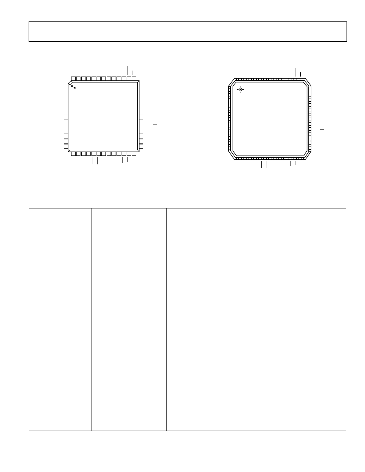
Figure 2. 52-Lead MQFP Pin Configuration
PSEN
EA
C)
2
P3.7/RD
SCLOCK (I
39
38
37
36
35
34
33
32
31
30
29
28
27
P2.7/PWMCLK
P2.6/PWM1
P2.5/PWM0
P2.4/T2EX
DGND
DV
DD
XTAL2
XTAL1
P2.3/SS/T2
P2.2/MISO
P2.1/MOSI
P2.0/SCLOCK (SPI)
SDATA
P1.0/AIN1
P0.7/AD7
55
56
AV
AGND
AGND
DAC
1
2
PIN 1
IDENTIFIER
3
4
DD
5
6
ADuC845/ADuC847/ADuC848
7
8
9
10
11
12
13
14
15161718192021222324252627
AIN9
AIN10
P1.1/AIN2
P1.2/AIN3/REFIN2+
P1.3/AIN4/REFIN2–
REFIN–
REFIN+
P1.4/AIN5
P1.5/AIN6
P1.6/AIN7/IEXC1
P1.7/AIN8/IEXC2
AINCOM/DAC
04741-002
Figure 3. 56-Lead LFCSP Pin Configuration
Table 3. Pin Fu
in No: Pin No: 56-
P
52-MQFP LFCSP Mnemonic
1 56 P1.0/AIN1 I B
nction Descriptions
Typ e
1
Description
y power-on default, P1.0/AIN1 is configured as the AIN1 analog input.
AIN1 can be u
sed as a pseudo differential input when used with AINCOM or as
the positive input of a fully differential pair when used with AIN2.
P1.0 has no digital output driver. It can function as a digital input for which 0
must be written to the port bit. As a digital input, this pin must be driven high
or low externally.
2 1 P1.1/AIN2 I
On power-on default, P1.1/AIN2 is configured as the AIN2 analog input.
AIN2 can be used as a pseudo differential input when used with AINCOM or as
the negative input of a fully differential pair when used with AIN1.
P1.1 has no digital output driver. It can function as a digital input for which 0
must be written to the port bit. As a digital input, this pin must be driven high
or low externally.
3 2 P1.2/AIN3/REFIN2+ I
On power-on default, P1.2/AIN3 is configured as the AIN3 analog input.
AIN3 can be used as a pseudo differential input when used with AINCOM or as
the positive input of a fully differential pair when used with AIN4.
P1.2 has no digital output driver. It can function as a digital input for which 0
must be written to the port bit. As a digital input, this pin must be driven high
or low externally. This pin also functions as a second external differential
reference input, positive terminal.
4 3 P1.3/AIN4/REFIN2− I
On power-on default, P1.3/AIN4 is configured as the AIN4 analog input.
AIN4 can be used as a pseudo differential input when used with AINCOM or as
the negative input of a fully differential pair when used with AIN3.
P1.3 has no digital output driver. It can function as a digital input for which 0
must be written to the port bit. As a digital input, this pin must be driven high
or low externally. This pin also functions as a second external differential
reference input, negative terminal.
5 4 AV
DD
S Analog Supply Voltage.
6 5 AGND S Analog Ground.
--- 6 AGND S A second analog ground is provided with the LFCSP version only.
7 7 REFIN− Reference Input, Negative Terminal. I External Differential
8 8 REFIN+ I External Differential Reference Input, Positive Terminal.
Footnotes at end of table.
P2.7/PWMCLK
P2.6/PWM1
P2.5/PWM0
P2.4/T2EX
DGND
DGND
DV
DD
XTAL2
XTAL1
P2.3/SS/T2
P2.2/MISO
P2.1/MOSI
P2.0/SCLOCK (SPI)
SDATA
04741-003
Rev. B | Page 11 of 108
ADuC845/ADuC847/ADuC848
Pin No:
52-MQFP
9 9 P1.4/AIN5 analog input.
10 10 P1.5/AIN6 I
11 11 P1.6/AIN7/IEXC1 I/O
12 12 P1.7/AIN8/IEXC2 I/O
13 13 AINCOM/DAC I/O
14 14 DAC O The voltage output from the DAC, if enabled, appears at this pin.
---- 15 AIN9 I
---- 16 AIN10
15 17 RESET I
16–
19
22–25
16 18 P3.0/RxD Receiver Data for UART Serial Port.
17 19 P3.1/TxD Transmitter Data for UART Serial Port.
18 20
19 21
22 24 P3.4/T0 Timer/Counter 0 External Input.
23 25 P3.5/T1 Timer/Counter 1 External Input.
24 26
25 27
Pin No: 56LFCSP
21
18–
24–27
Mnemonic
.7
P3.0–P3
INT0
P3.2/
INT1
P3.3/
WR
P3.6/
RD
P3.7/
Typ e
I On power-on default, P1.4/AIN5 is configured as the AIN5
I
I/O
r 0. External Interrupt 0. This pin can also be used as a gate control input to Time
External Interrupt 1. This pin can also be used as a gate control input to Timer 1.
1
Description
AIN5 can be used as a pseudo differential input when us
the positive input of a fully differential pair when used with AIN6.
P1.0 has no digital output driver. It can function as a digital input for whic
must be written to the port bit. As a digital input, this pin must be driven high
or low externally.
On power-on default, P1.5/AIN6 is configured as the AIN6 analog input.
AIN6 can be used as a pseudo differential input when used with AINCOM or as
the negative input
P1.1 has no digital output driver. It can function as a digital input for whic
must be written to the port bit. As a digital input, this pin must be driven high
or low externally.
On power-on default, P1.6/AIN7 is configured as the AIN7 analog input.
AIN7 can be used as a pseudo differential input when used with AINCOM or as
the positive input
current sources can also be configured at this pin.
P1.6 has no digital output driver. It can, however, function as a digital input for
which 0 must be written to the port bit. As a digital input, this pin must be
driven high or low externally.
On power-on default, P1.7/AIN8 is configured as the AIN8 analog input.
AIN8 can be used as a pseudo differential input when used with AINCOM or
the negative input of a fully dif
both current sources can also be configured at this pin.
P1.7 has no digital output driver. It can, however, function as a digital input for
which 0 must be written to the port bit. As a digital input, this pin must be
driven high or low externally.
All analog inputs can be referred to this pin, provided that a relevant pseudo
differential input mode is selected. This pin also functions as an alternative pin
out for the DAC.
AIN9 can be used as a pseudo differential analog input when used with
AINCOM or as the
AIN10 (LFCSP version only).
AIN10 can be used as a pseudo differential analog input when used with
AINCOM or as the negative input of a fully differential pair when used with
AIN9 (LFCSP version only).
Reset Input. A high level on this pin for 16 core clock cycles while the
oscillator is running resets the device. This pin has an internal weak pull-dow
and a Schmitt trigger input stage.
P3.0 to P3.7 are bidirectional port pins with internal pull-up resistors. P
pins that have 1s written to them are pulled high by the internal pull-up
resistors, and in that state can be used as inputs. As inputs, Port 3 pins being
pulled externally low source current because of the internal pull-up resistors
When driving a 0-to-1 output transition, a strong pull-up is active for one cor
clock period of the instruction cycle.
Port 3 pins also have the various secondary functions described below.
External Data Memory Write Strobe. This pin latches the data byte from Port 0
into an external data memory.
External Data Memory Read Strobe. This pin enables the data from an external
data memory to Port 0.
of a fully differential pair when used with AIN5.
of a fully differential pair when used with AIN8. One or both
ferential pair when used with AIN7. One or
positive input of a fully differential pair when used with
ed with AINCOM or as
ort 3
h 0
h 0
as
n
.
e
Rev. B | Page 12 of 108

ADuC845/ADuC847/ADuC848
Pin No:
52-MQFP
20, 34, 48
21, 35, 47
26 28 SCLK (I2C) I/O
27 29 SDATA I/O
28–31,
39
36– 42
28 30 P2.0/SCLOCK (SPI)
29 31 P2.1/MOSI
30 32 P2.2/MISO
31 33
36 39 P2.4/T2EX
37 40 P2.5/PWM0 0 output appears at this pin. If the PWM is enabled, the PWM
38 41 P2.6/PWM1 If the PWM is enabled, the PWM1 output appears at this pin.
39 42 P2.7/PWMCLK provided at this pin. If the PWM is enabled, an external PWM clock can be
32 34 XTAL1 I Input to the Crystal Oscillator Inverter.
33 35 XTAL2 O
40 43
41 44
42 45 ALE O
Pin No: 56LFCSP
22, 36, 51
7, 38, 50
23, 3
30–33, 39–
Mnemonic
DV
DD
DGND S Digital Ground.
Typ e
1
Description
S Digital Supply Voltage.
Serial Interface Clock for the I
triggered input. A weak
outputting logic
internal pull-up is present on this pin unless it is
low. This pin can also be controlled in software as a digital
2
C Interface. As an input, this pin is a Schmitt-
output pin.
2
Serial Data Pin for the I
C Interface. As an input, this pin has a weak intern
pull-up present unless it is outputting logic low.
P2.0–P2.7 I/O
Port 2 is a bid
irectional port with internal pull-up resistors. Port 2 pins that
have 1s written to them are pulled high by the internal pull-up resistors, and
in that state can be used as inputs. As inputs, Port
externally low source current because of the internal pull-up resistors. Port 2
emits the middle and high-order address bytes during accesses to the 24-bit
external data memory space.
Port 2 pins also have the various secondary functions described below.
Serial Interface Clock for the SPI Interface. As an input this pin is a Schmitt-
triggered input. A weak interna
outputting logic low.
Serial Master Output/Slave Input Data for the SPI Interface. A strong interna
pull-up is present on this pin when the SPI interface outputs a logic high.
strong internal pull-do
wn is present on this pin when the SPI interface
outputs a logic low.
Master Input/Slave Output for the SPI Interface. A weak pull-up is present on
this input pin.
P2.3/SS
/T2
Slave Select Input for the SPI
Interface. A weak pull-up is present on this pin.
For both package options, this pin can also be used to provide a clock input to
Timer 2. When e
nabled, Counter 2 is incremented in response to a negative
transition on the T2 input pin.
Control Input to Timer 2. When enabled, a negative transition on the T2EX
input pin causes a Timer 2 capture or reload event.
Output from the Crystal Oscillator Inverter. See the Hardware Desig
Considerations section for a description.
EA
External Access Enable, Logic Input. When held high, this input enables the
device to fetch code from internal program memory locations 0000H
F7FFH. No external program memory acce
ADuC847, or ADuC848. To determine the mode of code execution, the
is sampled at the end of an external RESET assertion or as part of a device
power cycle.
EA can also be used as an external emulation I/O pin, and
therefore the voltage level at this pin must not be changed during normal
operation because this might cause an emulation interrupt that halts code
execution.
PSEN
O
Program Store Enable, Logic Output. This function is not used on the
ADuC845, ADuC847, or ADuC848. This pin remains high during internal
program exe
cution.
PSEN can also be used to enable serial download mode when pulled lo
through a resistor at the end of an external RESET assertion or as part o
device power cycle.
Address Latch Enable, Logic Output. This output is used to latch the low by
(and page byte for 24-bit data address space accesses) of the address to
external memory dur
ing external data memory access cycles. It can be
disabled by setting the PCON.4 bit in the PCON SFR.
2 pins being pulled
l pull-up is present on this pin unless it is
n
to
ss is available on the ADuC845,
al
A
EA pin
w
f a
te
l
Rev. B | Page 13 of 108

ADuC845/ADuC847/ADuC848
Pin No:
52-MQFP
43–46,
49–52
1
I = input, O = output, S = supply.
Pin No: 56LFCSP
46–49, 52–
55
Mnemonic
P0.0–P0.7
Typ e
I/O
1
Description
These pins are part of Port 0, which is an 8-bit open-d
rain bidirectional I/O
port. Port 0 pins that have 1s written to them float, and, in that state, can be
used as high impedance inputs. An external pull-up resistor is required on P0
outputs to force a valid logic high level externally. Port 0 is also the
multiplexed low-order address and data bus during accesses to external data
memory. In this application, Port 0 uses strong internal pull-ups when
emitting 1s.
Rev. B | Page 14 of 108

ADuC845/ADuC847/ADuC848
GENERAL DESCRIPTION
The AD
12.58 M
ADuC836. They include additional analog inputs for
applications requiring more ADC channels.
The ADuC845, ADuC847, and ADuC848 are complete smar
transducer front ends. The family integrates high resolution
Σ-Δ ADCs with flexible, up to 10-channel, input multiplexing, a
f
sin
The ADuC845 includes two (primary and auxiliary) 24-bit Σ-Δ
ADCs with internal buffering and PGA on the primary ADC.
The ADuC847 includes the same primary ADC as the ADuC845
(auxiliary ADC removed). The ADuC848 is a 16-bit ADC
version of the ADuC847.
The ADCs incorporate flexible input multiplexing, a temperature
sensor (ADuC845 only), and a PGA (primary ADC only)
allowing direct measurement of low-level signals. The ADCs
include on-chip digital filtering and programmable output data
rates that are intended for measuring wide dynamic range and
low frequency signals, such as those in weigh scale, strain gage,
pressure transducer, or temperature measurement applications.
uC84 7, 848 are singl le,
5, ADuC84 and ADuC e-cyc
IPs, 8052 core upgr es to the ADuC834 and
ast 8-bit MCU, and program and data Flash/EE memory on a
gle chip.
ad
The devices operate from a 32 kHz crystal with an on-chip PL
generating a high frequency clock of 12.58 MHz. This clock is
routed through a programmable clock divider from which the
MCU core clock operating frequency is generated. The micro-
t
controller core is an optimized single-cycle 8052 offering
12.58 MIPs performance while maintaining 8051 instruction set
compatibility.
The available nonvolatile Flash/EE program memory options
are 62 kbytes, 32 kbytes, and 8 kbytes. 4 kbytes of nonvolatile
Flash/EE data memory and 2304 bytes of data RAM are also
provided on-chip. The program memory can be configured as
data memory to give up to 60 kbytes of NV data memory in
data logging applications.
On-chip factory firmware supports in-circuit serial download
and debug modes (via UART), as well as single-pin emulation
mode via the
are supported by the QuickStart™ development system featuring
low cost software and hardware development tools.
pin. The ADuC845, ADuC847, and ADuC848
EA
L
up to
Rev. B | Page 15 of 108
ADuC845/ADuC847/ADuC848
K
A
C
P0.0 (AD0)
P0.1 (AD1)
P0.2 (AD2)48P0.3 (AD3)49P0.4 (AD4)52P0.5 (AD5)53P0.6 (AD6)54P0.7 (AD7)
AIN1
AIN2
AIN3
AIN4
AIN5
AIN6
AIN7
AIN8
AIN9
AIN10
INCOM/DA
REFIN+
REFIN–
IEXC1
IEXC2
46 47
56
1
2
3
9
10
11
12
15
16
13
8
7
AIN
MUX
TEMP
SENSOR
200µA200µA
CURRENT
11
SOURCE
12
MIX
4 36 51 23 37 38 50 1817 19 44 43 45 30 31 32 33 28 29 34 35
5 6 22
DD
AV
AGND
NOTES
1. THE PIN NUMBERS REFER TO THE LFCSP PACKAGE ONLY.
BUF
AUXILIARY ADC
BAND GAP
REFERENCE
DD
DV
55
24-BIT
Σ-∆ ADC
V
REF
DETECT
POR
DGND
6)P2.0/SCLK (A8/A1
P1.0/AIN1
P1.1/AIN2
P1.2/AIN3/REFIN2+
56 1
P1.3/AIN4/REFIN2–3P1.4/AIN59P1.5/AIN610P1.6/AIN7/IEXC1
2
P1.7/AIN8/IEXC2
11
12
P2.1/MOSI (A9/A17)
P2.2/MISO (A10/A18)32P2.3/SS/T2 (A11/A19)33P2.4/T2EX (A12/A20)39P2.5/PWM0 (A13/A21)40P2.6/PWM1 (A14/A22)41P2.7/PWMCLK (A15/A23)
30 31
ADuC845
PGA
T
24-BI
Σ-∆ ADC
ADC
CONTR
AND
FLASH/EE
FLASH/EE
DOWDENLOADER
UART
TxD
RxD
C
NTERS
POINTER
BUGGER
PRIMARY AD
CALIBRATIOOLN
62 kBYTES PROGRAM/
4 kBYTES DATA/
2 × DATA POI
11-BIT STACK
SERIAL PORT
ESETR
ADC
C
ONTROL
AND
CA
LIBRATION
UART
TIMER
SINGLE-
CYCLE
8052
MCU
CORE
PSEN
Figure 4. Detailed Block Diagram of the ADuC845
EMULATOR
SINGLE-PIN
EA
CONTROL
ALE
42
DAC
PWM
CONTROL
2304 BYTES
USER RAM
WATCHDOG
TIMER
POWER SUPPLY
MONITOR
SPI SERIAL
INTERFACE
MOSI
SCLK
P3.0 (RxD)
P3.1 (TxD)
18 19
12-BIT
VOLTAGE
OUTPUT DAC
DUAL
16-BIT
Σ-∆ DAC
DUAL
16-BIT
PWM
PLL WITH PROG.
CLOCK DIVIDER
WAKE-UP/
RTC TIMER
I2C SERIAL
INTERFACE
SS
MISO
P3.2 (INT0)20P3.3 (INT1)21P3.4 (T0)24P3.5 (T1)25P3.6 (WR)26P3.7 (RD)
BUF
MUX
16-BIT
COUNTER
TIMERS
OSC
SCLK
SDATA
XTAL1
XTAL2
27
14
DAC
40
PWM0
41
PWM1
42
PWMCL
24
T0
25
T1
33
T2
39
T2EX
20
INT0
21
INT1
04741-004
Rev. B | Page 16 of 108
ADuC845/ADuC847/ADuC848
K
A
C
P0.0 (AD0)
P0.1 (AD1)
AIN1
AIN2
AIN3
AIN4
AIN5
AIN6
AIN7
AIN8
AIN9
AIN10
INCOM/DA
REFIN+
REFIN–
IEXC1
IEXC2
P0.2 (AD2)48P0.3 (AD3)49P0.4 (AD4)52P0.5 (AD5)53P0.6 (AD6)54P0.7 (AD7)
46 47
56
1
2
3
9
10
11
12
15
16
13
8
7
AIN
MUX
55
BUF
BAND GAP
REFERENCE
200µA200µA
CURRENT
11
SOURCE
12
MIX
4 36 51 23
5 6 22
DD
AV
AGND
NOTES
1. THE PIN NUMBERS REFER TO THE LFCSP PACKAGE ONLY.
DD
DV
P1.0/AIN1
P1.1/AIN2
P1.2/AIN3/REFIN2+
P1.3/AIN4/REFIN2–3P1.4/AIN59P1.5/AIN610P1.6/AIN7/IEXC1
2
PRIMARY ADC
24-BIT
Σ-∆ ADC
62 kBYTES PROGRAM/
FLASH/EE
4 kBYTES DATA/
FLASH/EE
2 × DATA POINTERS
11-BIT STACK POINTER
V
REF
DETECT
56 1
PGA
DOWNLOADER
POR
37 38 50 1817 19 44 43 45 30 31 32 33 28 29 34 35
DGND
UART
SERIAL PORT
RESET
RxD
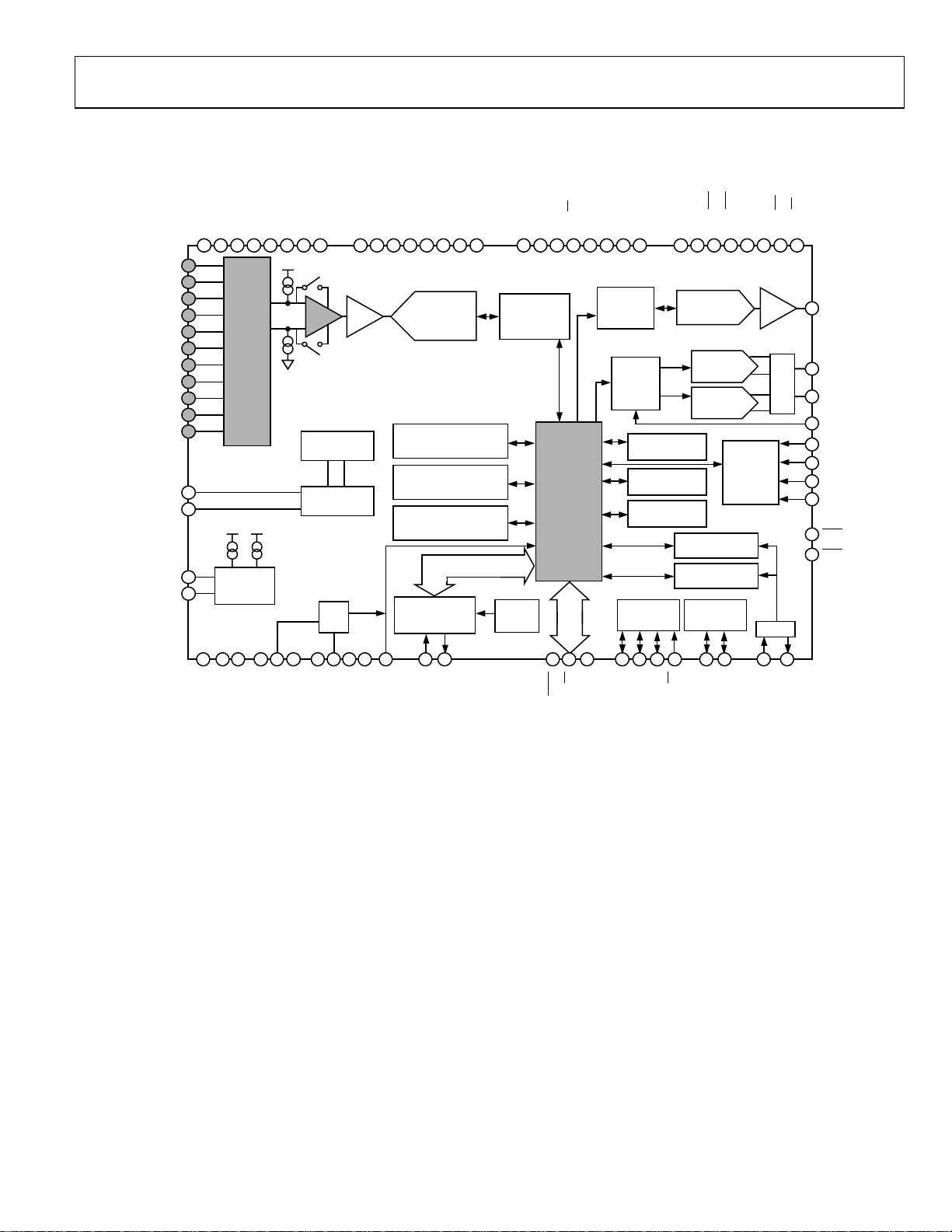
Figure 5. Detailed Block Diagram of the ADuC847
P1.7/AIN8/IEXC212P2.0/SCLK (A8/A16)
11
ADuC847
DEBUGGER
TxD
P2.1/MOSI (A9/A17)
30 31
ADC
CONTROL
AND
CALIBRATION
SINGLE-
CYCLE
CORE
UART
TIMER
P2.2/MISO (A10/A18)32P2.3/SS/T2 (A11/A19)33P2.4/T2EX (A12/A20)39P2.5/PWM0 (A13/A21)40P2.6/PWM1 (A14/A22)41P2.7/PWMCLK (A15/A23)
DAC
CONTROL
PWM
CONTROL
8052
MCU
SINGLE-PIN
PSEN
EMULATOR
EA
ALE
POWER SUPPLY
SPI SERIAL
INTERFACE
SCLK
42
P3.0 (RxD)
18 19
OUTPUT DAC
2304 BYTES
USER RAM
WATCHDOG
TIMER
MONITOR
PLL WITH PROG.
CLOCK DIVIDER
SS
MOSI
MISO
P3.1 (TxD)
P3.2 (INT0)20P3.3 (INT1)21P3.4 (T0)24P3.5 (T1)25P3.6 (WR)26P3.7 (RD)
12-BIT
VOLTAGE
DUAL
16-BIT
Σ-∆ DAC
DUAL
16-BIT
PWM
16-BIT
COUNTER
TIMERS
WAKE-UP/
RTC TIMER
I2C SERIAL
INTERFACE
SCLK
SDATA
BUF
OSC
XTAL1
MUX
27
14
DAC
40
PWM0
41
PWM1
42
PWMCL
24
T0
25
T1
33
T2
39
T2EX
20
INT0
21
INT1
XTAL2
04741-070
Rev. B | Page 17 of 108
ADuC845/ADuC847/ADuC848
K
A
C
P0.0 (AD0)
P0.1 (AD1)
P0.2 (AD2)48P0.3 (AD3)49P0.4 (AD4)52P0.5 (AD5)53P0.6 (AD6)54P0.7 (AD7)
AIN1
AIN2
AIN3
AIN4
AIN5
AIN6
AIN7
AIN8
AIN9
AIN10
INCOM/DA
REFIN+
REFIN–
IEXC1
IEXC2
46 47
56
1
2
3
9
10
11
12
15
16
13
8
7
11
12
NOTES
1. THE PIN NUMBERS REFER TO THE LFCSP PACKAGE ONLY.
AIN
MUX
200µA200µA
CURRENT
SOURCE
MIX
4 36 51 23 37 38 50 1817 19 44 43 45 30 31 32 33 28 29 34 35
5 6 22
DD
AV
AGND
DD
DV
55
BUF
BAND GAP
REFERENCE
V
REF
DETECT
POR
DGND
P1.0/AIN1
P1.1/AIN2
P1.2/AIN3/REFIN2+
56 1
P1.3/AIN4/REFIN2–3P1.4/AIN59P1.5/AIN610P1.6/AIN7/IEXC1
2
P1.7/AIN8/IEXC212P2.0/SCLK (A8/A16)
11
P2.1/MOSI (A9/A17)
P2.2/MISO (A10/A18)32P2.3/SS/T2 (A11/A19)33P2.4/T2EX (A12/A20)39P2.5/PWM0 (A13/A21)40P2.6/PWM1 (A14/A22)41P2.7/PWMCLK (A15/A23)
30 31
ADuC848
PGA
11-BIT STACK POINTER
RESET
PRIMARY ADC
16-BIT
Σ-∆ ADC
62 kBYTES PROGRAM/
FLASH/EE
4 kBYTES DATA/
FLASH/EE
2 × DATA POINTERS
DOWNLOADER
DEBUGGER
UART
SERIAL PORT
TxD
RxD
ADC
CONTROL
AND
CALIBRATION
SINGLE-
CYCLE
UART
TIMER
8052
MCU
CORE
PSEN
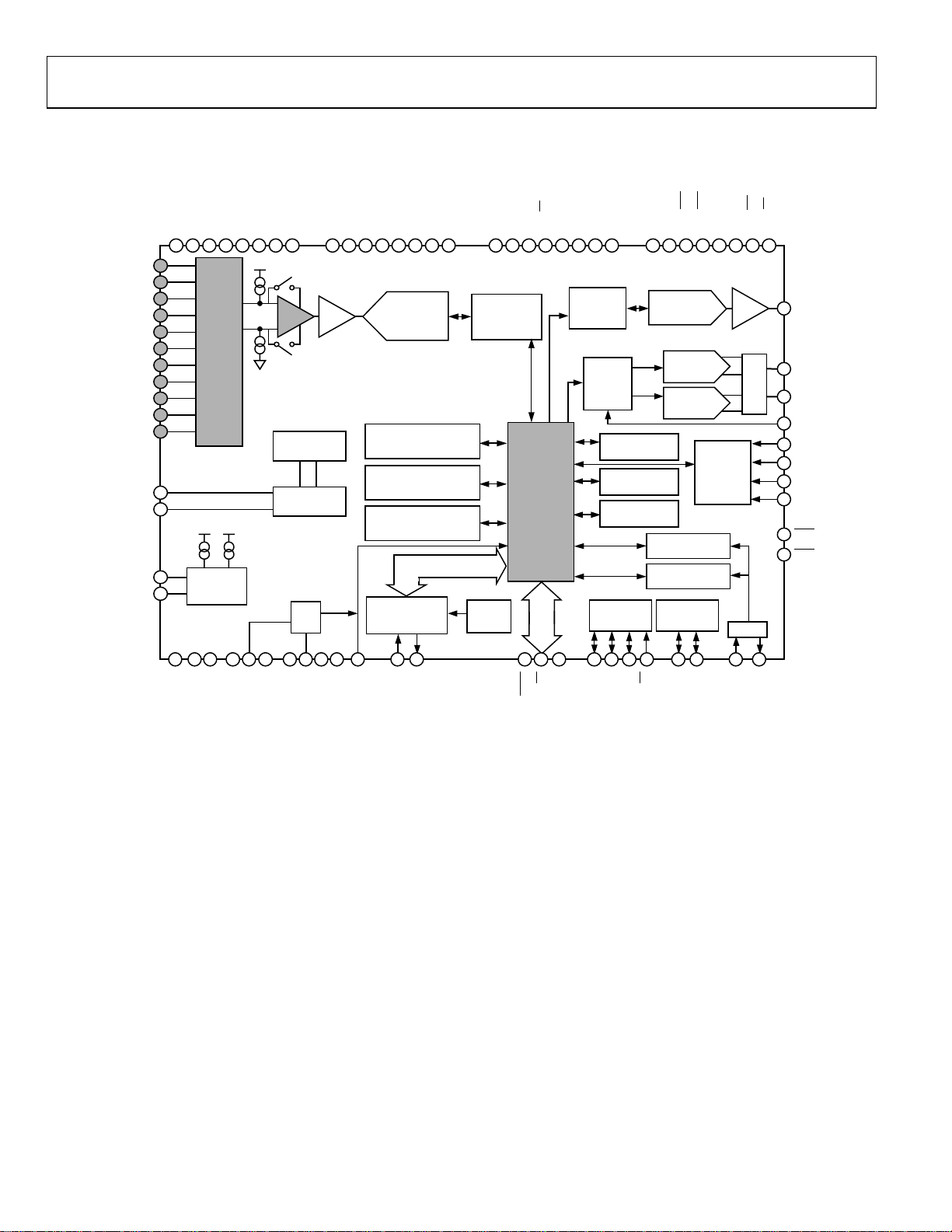
Figure 6. Detailed Block Diagram of the ADuC848
EMULATOR
SINGLE-PIN
EA
CONTROL
ALE
42
DAC
PWM
CONTROL
2304 BYTES
USER RAM
WATCHDOG
TIMER
POWER SUPPLY
MONITOR
SPI SERIAL
INTERFACE
MOSI
SCLK
P3.0 (RxD)
P3.1 (TxD)
18 19
12-BIT
VOLTAGE
OUTPUT DAC
DUAL
16-BIT
Σ-∆ DAC
DUAL
16-BIT
PWM
PLL WITH PROG.
CLOCK DIVIDER
WAKE-UP/
RTC TIMER
I2C SERIAL
INTERFACE
SS
MISO
P3.2 (INT0)20P3.3 (INT1)21P3.4 (T0)24P3.5 (T1)25P3.6 (WR)26P3.7 (RD)
BUF
MUX
16-BIT
COUNTER
TIMERS
OSC
SCLK
XTAL1
SDATA
27
14
DAC
40
PWM0
41
PWM1
42
PWMCL
24
T0
25
T1
33
T2
39
T2EX
20
INT0
21
INT1
XTAL2
04741-072
8052 INSTRUCTION SET
Table 4 documents the number of clock cycles required for each
instruction. Most instructions are executed in one or two clock
cycles resulting in 12.58 MIPs peak performance when operating
at PLLCON = 00H.
TIMER OPERATION
Timers on a standard 8052 increment by one with each machine
ALE
On the ADuC834, the output on the ALE pin is a clock at 1/6th
of the core operating frequency. On the ADuC845, ADuC847,
and ADuC848, the ALE pin operates as follows. For a single
machine cycle instruction, ALE is high for the entire machine
cycle. For a two or more m
for the first machine cycle and then low for the remainder of the
machine cycles.
achine cycle instruction, ALE is high
cycle. On the ADuC845, ADuC847, and ADuC848, one
machine cycle is equal to one clock cycle; therefore, the timers
increment at the same rate as the core clock.
EXTERNAL MEMORY ACCESS
The ADuC845, ADuC847, and ADuC848 do not support
external program memory access, but the parts can access up to
16 MB (24 address bits) of external data memory. When
accessing external RAM, the EWAIT register might need to be
programmed in order to give extra machine cycles to MOVX
commands to allow for differing external RAM access speeds.
Rev. B | Page 18 of 108
ADuC845/ADuC847/ADuC848
COMPLETE SFR MAP
ISPI
WCOL
SPE
SPIM
CPO
CPHA
SPR1
FFH 0
FEH 0
FDH 0
FCH 0
FBHL0
FAH
1
F7H 0 F6H 0 F5H 0 F4H 0 F3H 0 F2H F1H 0 F0H 0
MDO
EFH 0 EEH 0
E7H 0 E6H 0 E5H 0 E4H 0 E3H 0 E2H E1H 0 E0H 0
RDY0
DFH 0
CY
D7H 0ACD6H 0F0D5H 0
TF2
CFH 0 CEH 0
PRE3
C7H 0 C6H
BFH 0 BEH 0
RD
B7H 1WRB6H 1T1B5H 1T0B4H 1
EA
AFH AEH
0
1
A7H A6H A5H 1 A4H 1 A3H 1 A2H A1H 1 A0H 1
SM0
9FH 0
97H 1 96H 1 95H 1 94H 1 93H 1 92H
TF1
8FH 0 8EH
87H 1 86H 1 85H 1 84H 1 83H 1 82H 81H 1 80H 1
MCO
MDE
RDY1
DEH 0
EXF2 RCLK
PRE20PRE1
PADC PT2
EADC ET2
00
1
SM1
9EH 0
TR10TF0
MDI
EDH 0 ECH 0 EBH 0 EAH E9H
CAL
NOXREF
DDH 0
DCH 0
DBH 0
RS1
D4H 0
D3H 0OVD2HFID1H 0PD0H 0
TCLK
CCH 0
PRE0
REN
9CH 0
TR0
8CH 0
EXEN2
CBH 0
C3H 0
BBH 0
B3H 1
ABH 0
9BH 0
8BH 0
CDH 0
C5H 0 C4H 1
BDH 0PSBCH 0
ADHESACH 0
SM2
9DH 0
8DH 0
I2CM
ERR0
RS0
WDIR
PT1
INT1
ET1
TB8
IE1
0
I2CRS I2CTX I2CI
0
0
ERR1
0
DAH D9H 0 D8H 0
0
TR2
0
CAH
WDS
0
C2H
PX1
0
BAH
INT0
B2H
1
EX1
0
AAH
1
RB8
9AHTI99H 0 98H 0
0
1
IT1
0
8AH
1
SPR0
F9H 0
F8H 0
0 E8H 0
CNT2
CAP2
C9H 0 C8H 0
WDE
WDWR
C1H 0 C0H 0
PT0
PX0
B9H 0
B8H 0
TxD
RxD
B1H 1
B0H 1
ET0
EX0
A9H 0
A8H 0
RI
T2EX
IE0
T2
90H 1
IT0
88H 0
91H 1
89H 0
BITS
BITS
BITS
BITS
BITS
BITS
BITS
BITS
BITS
BITS
BITS
BITS
BITS
BITS
BITS
BITS
SPICON
F8H 05H
RESERVED
B
F0H 00H
I2CCON
H 00H
E9H xxH EAH xxH EBH xxH ECH xxH EDHE8
ACC
E0H 00H
ADCSTAT
D8H 00H
E1H xxH
NOT AVAILABLE
PSW ADC
D0H 00H
C8H 00H
T2CON
D1H 08H
RESERVE
WDCON
C0H 10H
IP
B8H 00H
B9H 00H
P3
FFH
B0H
IE
A8H 00HIEA9H
P2
A0H FFH
A1H
SCON
00H98H
99H 00H
P1
90H FFH
TCON
88H 00H
89H 00H
P0
H FFH80
81H 07H
RESERVED
GN0L
OF0L
MODE
I2CADD1
F2H 7FH
2
GN0M2GN0H2GN1L2GN1
OF0M
E2H xxH
ADC0M
00HD9H
DAH 00H
ADC0C
D2H
RCAP2L
D
CAH 00H
HIPID
C
C2H A0H
RESERVED
RESERVED
ADC0L
ON ADuC848
RESERVED
ECON
PWM0L PWM0
B2H B3H
00H
IP2
A 0H
TIMECON
TMOD
HTHSEC
A2H A3H A4H
00H 00H 00H 00H
SBUF
I2CDAT
9AH 00H
TL0
8AH 00H
SP
DPL
82H 00H
DACL
FBH 00H
NOT USED
OF0H
E3H xxH
ADC0H
DBH 00H
ON1
ADC1CON
ADuC845 ONLY
07H
D3H 00HSFD4H 45H
RCAP2H
CBH 00H
RESERVED RESERVED
RESERVED
PWM1L PWM1H
H
00H
00H
1
1
SEC
I2CADD
9BH 55H
TL1
8BH 00H
DPH
83H 00H
DACH
DACCON
FCH 00H
ADuC845 ONLY ADuC845 ONLY
ADuC845 ONLY ADuC845 ONLY
E4H xxH
ADuC845 ONLY ADuC845 ONLY ADuC845 ONLY
DCH 00H
OF1L
ADC1M
FDH 00H
E5H
ADC
DDH 00H
D5H 00H
TL2
CCH 00H
EDATA1
BCH 00H
B4H
RESERVED
CDH 00H
RESER
EDAT
BDHA200H
00H
RESERRESERVEDRESERVEDRESERVED
1
MIN
HOU INTVA L
A5H
9DH 9EH 00H
TH0
8CH 00H
8DH 00H
DPP
84H 00H
RESERVED
RESVED ERVEDRESERRESERVED
2
H
RESERVED RESERVED
xxH
OF1
H
ADC0CON2
E6H 00H
xxH
ADC1L
1H
DEH 00H
ICON
RESERVED
TH2
RESERVED
EDARL
VED
C6H 00H
EDATA3
BEH 00H
RESERVEDRESERVED
PWMCON
VED
AEH
1
R
A6H H
00H
T3F T3CON
D
00H
TH1
RESERVED SERVED
RESERVEDRESER
VED
00H
00H
RESERVED
SPIDAT
F7H 00H
SERVED
RE
PSMCON
H DEH
DF
PLLCON
H 53H
D7
RESERVED
EDARH
H 00H
C7
DATA4
E
H 00H
BF
SPH
B7H
G845/7/8
CF
AFH
CON
DP
A7
AIT
EW
H 00H
9F
RESERVEDRESERVEDRESERVEDRESERVEDRESERVEDRESERVEDRESERVED
RE
PCON
H 00H
87
00HB1H
00H
00H
1
THESE SFR
2
CALIBRATION COEFFICIENTS ARE PRECONFIGURED ON POWER-UP TO FACTORY CALIBRATED VALUES.
s MAINTAIN THEIR PRE-RESET VALUES AFTER = 1.
R MAP KEY:
SF
A RESET IF TIMECON.0
THESE BITS ARE CONTAINED IN THIS BYTE.
BIT MNEMONIC
BIT ADDRESS
IE0
89H 0
IT0
88H 0
TCON
88H 00H
RESET DEFAULT BIT VALUE
NOTE:
SFR
s WHOSE ADDRESSES END IN 0H OR 8H ARE
SFR BIT ADDRESSABLE.
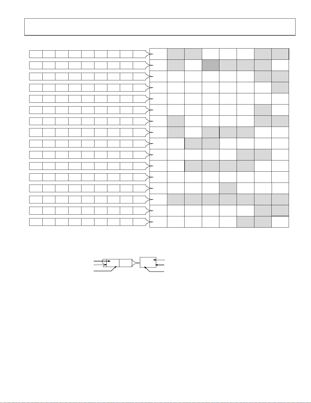
Figure 7. e ADuC845, ADuC847, and ADuC848
Complete SFR Map for th
MNEMONIC
RESET DEFAUL
SFR ADDRESS
T VALUE
04741-073
Rev. B | Page 19 of 108

ADuC845/ADuC847/ADuC848
FUNCTIO
8051
Table 4 tion Set
Mnemonic D B C
Arithmetic
A A,Rn Add register to A 1 1
ADD A,@Ri Add indirect memory to A 1 2
ADD A,dir Add direct byte to A 2 2
ADD A,#data Add immediate to A 2 2
ADDC A,Rn Add register to A with carry 1 1
ADDC A,@Ri Add indirect memory to A with carry 1 2
ADDC A,dir ith carry Add direct byte to A w 2 2
ADD A,#data Add immediate to A with carry 2 2
SUBB A,Rn Subtract register from A with borrow 1 1
SUBB A,@Ri Subtract indirect memory from A with borrow 1 2
SUBB A,dir Subtract direct from A with borrow 2 2
SUBB A,#data Subtract immediate from A with borrow 2 2
INC A Increment A 1 1
INC Rn Increment register 1 1
INC @Ri Increment indirect memory 1 2
INC dir Increment direct byte 2 2
INC DPTR Increment data pointer 1 3
DEC A Decrement A 1 1
DEC Rn Decrement register 1 1
DEC @Ri Decrement indirect memory 1 2
DEC dir Decrement direct byte 2 2
MUL AB Multiply A by B 1 4
DIV AB Divide A by B 1 9
DA A Decimal adjust A 1 2
Logic
ANL A,Rn AND register to A 1 1
ANL A,@Ri AND indirect memory to A 1 2
ANL A,dir AND direct byte to A 2 2
ANL A,#data iate to A AND immed 2 2
ANL dir,A AND A to direct byte 2 2
ANL dir,#data ediate data to direct byte AND imm 3 3
ORL A,Rn OR register to A 1 1
ORL A,@Ri to A OR indirect memory 1 2
ORL A,dir OR direct byte to A 2 2
ORL A,#data OR immediate to A 2 2
ORL dir,A OR A to direct byte 2 2
ORL dir,#data irect byte OR immediate data to d 3 3
XRL A,Rn Exclusive-OR register to A 1 1
XRL A,@Ri Exclusive-OR indirect memory to A 2 2
XRL A,#data Exclusive-OR immediate to A 2 2
XRL dir,A Exclusive-OR A to direct byte 2 2
XRL A,dir Exclusive-OR indirect memory to A 2 2
XRL dir,#data data to direct Exclusive-OR immediate 3 3
CLR A Clear A 1 1
CPL A Complement A 1 1
SWAP A Swap nibbles of A 1 1
RL A Rotate A left 1 1
NAL DESCRIPTION
INSTRUCTION SET
. Optimized Single-Cycle 8051 Instruc
escription ytes ycles
1
Rev. B | Page 20 of 108

ADuC845/ADuC847/ADuC848
Mnemonic Description Bytes Cycles
RLC A Rotate A left through carry 1 1
RR A Rotate A right 1 1
RRC A Rotate A right through carry 1 1
Data Transfer
MOV A,Rn Move register to A 1 1
MOV A,@Ri Move indirect memory to A 1 2
MOV Rn,A Move A to register 1 1
MOV @Ri,A Move A to indirect memory 1 2
MOV A,dir Move direct byte to A 2 2
MOV A,#data Move immediate to A 2 2
MOV Rn,#data Move register to immediate 2 2
MOV dir,A Move A to direct byte 2 2
MOV Rn, dir Move register to direct byte 2 2
MOV dir, Rn Move direct to register 2 2
MOV @Ri,#data Move immediate to indirect memory 2 2
MOV dir,@Ri Move indirect to direct memory 2
MOV @Ri,dir Move direct to indirect memory 2 2
MOV dir,dir te to direct byte Move direct by 3 3
MOV dir,#data Move immediate to direct byte 3 3
MOV DPTR,#data Move immediate to data pointer 3 3
MOVC A,@A+DPTR Move code byte relative DPTR to A 1 4
MOVC A,@A+PC Move code byte relative PC to A 1 4
MOVX2 A,@Ri Move external (A8) data to 1 4 A
MOVX2 A,@DPTR Move external (A16) data t 1 4 o A
MOVX2 @Ri,A Move A to external data (A8) 1 4
MOVX2 @DPTR,A Move A to external data (A16) 1 4
PU dir Push direct byteSH onto stack 2 2
POP dir Pop direct byte from stack 2 2
XCH Exchange A and register 1 1 A,Rn
XC A,@Ri ExH change A and indirect memory 1 2
XC D A,@Ri H Exchange A and indirect memory nibble 1 2
XCH A Exchange A and direct by,dir te 2 2
Boolean
CLR C Clear carry 1 1
CLR bit Clear direct bit 2 2
SETB C Set carry 1 1
SETB bit Set direct bit 2 2
CPL C Complement carry 1 1
CPL bit Complement direct bit 2 2
ANL C,bit AND direct bit and carry 2 2
ANL C,/bit AND direct bit inverse to carry 2 2
ORL C,bit OR direct bit and carry 2 2
ORL C,/bit OR direct bit inverse to carry 2 2
MOV C,bit Move direct bit to carry 2 2
MOV bit,C Move carry to direct bit 2 2
Branching
JMP @A+DPTR Jump indirect relative to DPTR 1 3
RET Return from subroutine 1 4
RETI Return from interrupt 1 4
ACALL addr11 Absolute jump to subroutine 2 3
AJMP addr11 Absolute jump unconditional 2 3
Footnotes at end of table.
2
1
Rev. B | Page 21 of 108

ADuC845/ADuC847/ADuC848
Mnemoni ption c Descri Bytes Cycles
SJMP rel Short jump (relative address) 2 3
JC rel Jump on carry = 1 3 2
JNC rel Jump on carry = 0 2 3
JZ rel Jump on accumulator = 0 2 3
JNZ rel Jump on accumulator ! = 0 2 3
DJNZ Rn,rel Decrement register, JNZ relative 2 3
LJMP Long jump unconditional 3 4
LCALL3 addr16 Long jump to subroutine 3 4
JB bit,rel Jump on direct bit = 1 3 4
JNB bit,rel Jump on direct bit = 0 4 3
JBC bit,rel Jump on direct bit = 1 and clear 3 4
CJNE A,dir,rel Compare A, direct JNE rela 4 tive 3
CJNE A,#data,rel Compare A, immediate JNE relative 3 4
CJNE Rn,#data,rel Compare register, immediate JNE relative 3 4
CJNE @Ri,#data,rel Compare indirect, immediate JNE relative 3 4
DJNZ dir,rel Decrement direct byte, JNZ relative 3 4
Miscellaneous
NOP No operation 1 1
1
1
One cycle is one clock.
2
MOVX instructions are four cycles when they have 0 wait state. Cycles of MOVX instructio AIT.
3
LCALL instructions are three cycles when the LCALL instruction comes from an interrupt.
MEMORY ORGANIZATION
The ADuC845, ADuC847, and ADuC848 contain four memory
blocks:
• 62 kbytes/3 h/EE program
memory
• 4 kbytes of on-chip Flash/EE data memory
• 256 bytes of general-purpose RAM
• 2 kbytes of internal XRAM
Flash/EE Program Memory
The parts provide up to 62 kbytes of Flash/EE program memory
to run user code. All further references to Flash/EE program
2 kbytes/8 kbytes of on-chip Flas
ns are 4 + n cycles when they have n wait states as programmed via EW
Flash/EE Data Memory
The user has 4 kbytes of Flash/EE data memory available that
can be accessed indirectly by using a group of registers mapped
into the sp
the Nonvola
General-Purp e
The general-purpos AM i
memories, the upp nd th
lower 128 bytes of RAM can be accessed through direct or
ecial function register (SFR) space. For details, see
tile Flash/EE Memory Overview section.
os RAM
e R s divided into two separate
er a e lower 128 bytes of RAM. The
indirect addressing. The upper 128 bytes of RAM can be
accessed only through indirect addressing because it shares th
same address space as the SFR space, which must be accessed
through direct addressing.
e
memory assume the 62-kbyte option.
The lower 128 bytes of internal data memory are mapped as
When
hardware reset, the parts default to code execution from their
internal 62 kbytes of Flash/EE program memory. The parts do
not support the rollover from internal code space to external
code space. No external code space is available on the parts.
Permanently embedded firmware allows code to be serially
downloaded to the 62 kbytes of internal code space via the
UART serial port while the device is in-circuit. No external
hardware is required.
During run time, 56 kbytes of the 62-kbyte program memory
can be reprogrammed. This means that the code space can be
upgraded in the field by using a user-defined protocol running
on the parts, or it can be used as a data memory. For details, see
is pulled high externally during a power cycle or a
EA
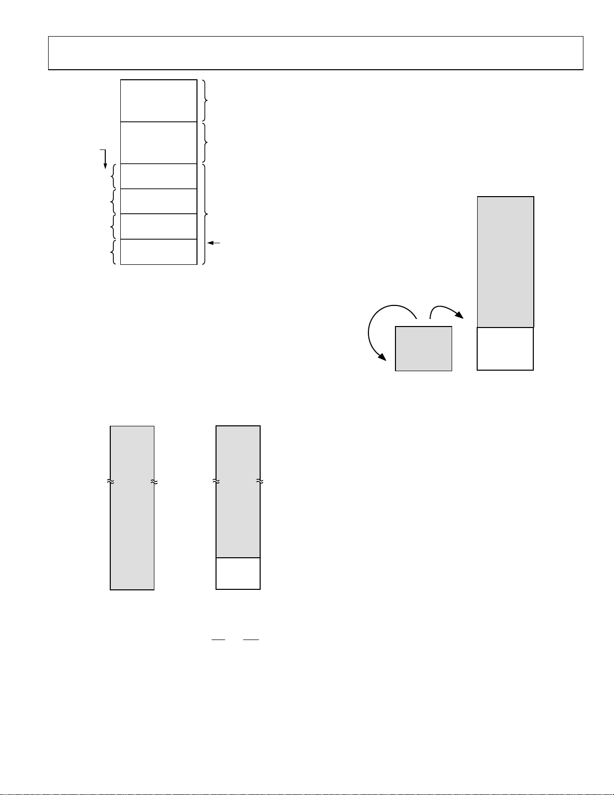
shown in Figure 8. The lowest 32 bytes are grouped into four
banks of eight registers addressed as R0 to R7. The next 16 bytes
(128 bits), locations 20H to 2FH above the register banks, form
a block of directly addressable bit locations at Bit Addresses
00H to 7FH. The stack can be located anywhere in the internal
memory address space, and the stack depth can be expanded up
to 2048 bytes.
Reset initializes the stack pointer to location 07H. Any call or
push pre-increments the SP before loading the stack. Therefore,
loading the stack starts from location 08H, which is also the
first register (R0) of Register Bank 1. Thus, if one is going to use
more than one register bank, the stack pointer should be
initialized to an area of RAM not used for data storage.
the Nonvolatile Flash/EE Memory Overview section.
Rev. B | Page 22 of 108
ADuC845/ADuC847/ADuC848
7FH
GENERAL-PURPOSE
AREA
30H
2FH
BANKS
SELECTED
VIA
BITS IN PSW
20H
11
18H
10
10H
01
08H
00
00H
1FH
17H
0FH
07H
BIT-ADDRESSABLE
(BIT ADDRESSES)
FOUR BANKS OF EIGHT
REGISTERS
R0 TO R7
RESET VALUE OF
STACK POINTER
04741-008
Figure 8. Lower 128 Bytes of Internal Data Memory
Internal XRAM
The ADuC845, ADuC847, and ADuC848 contain 2 kbytes of
on-chip extended data memory. This memory, although onchip, is accessed via the MOVX instruction. The 2 kbytes of
internal XRAM are mapped into the bottom 2 kbytes of the
external address space if the CFG84x.0 (Table 7) bit is set;
otherwise, access to the external data memory occurs just like a
standard 8051.
Even with the CFG84x.0 bit set, access to the external (off chip),
XRAM occurs once the 24-bit DPTR is greater than 0007FFH.
FFFFFFH
EXTERNAL
DATA
MEMORY
SPACE
(24-BIT
ADSPDRESS
ACE)
FFFFFFH
EXTERNAL
DATA
MEMORY
SPACE
(24-BIT
ADDRESS
SPACE)
is possible (by setting C
enable the 11-bit extended stack pointer. In this case, the stack
rolls over from FFH in RAM to 0100H in XRAM.
The 11-bit stack pointer is visible in the SPH and SP SFRs. Th
SP SFR is located at 81H as with a standard 8052. The SPH SF
is located at B7H. The 3 LSBs of the SPH SFR contain the 3
extra bits nece
ssary to extend the 8-bit stack pointer in the SP
SFR into an 11-bit stack pointer.
CFG845/7/8.7 = 0
FFH
00H
Figure 10. Extended Stack Pointer Operation
External Data Memory (External XRAM)
There is no support for external progra
parts. Howeve ju
r, st like a standard 8051-compatible core, the
ADuC845/ADuC847/ADuC
memory using a M X ins
utomatically outputs the various control strobes required to
a
access the data memory. The parts, ho
16 Mbytes of external data memory. T
the 64 kb tes of ext al data memor
sta ible core. Se
Co tions for details.
y ern y space available on a
ndard 8051-compat e the Hardware Design
nsidera section
FG845.7/ADuC847.7/ADuC848.7) to
07FFH
UPPER 1792
BYTES OF
ON-CHIP XRAM
(DATA + STACK
FOR EXSP = 1,
DATA ONLY
FOR EXSP = 0)
CFG845/7/8.7 = 1
100H
256 BYTES OF
ON-CHIP DATA
RAM
(DATA +
STACK)
ON-CHIP XRAM
(DATA ONLY)
00H
LOWER 256
BYTES OF
04741-010
m memory access to the
848 can access external data
OV truction. The MOVX instruction
wever, can access up to
his is an enhancement of
e
R
000800H
000000H
0007FFH
000000H
CFG845/7/8.0 = 0
2 kBYTES
ON-CHIP
XRAM
CFG845/7/8.0 = 1
04741-009
Figure 9. Internal and External XRAM
When enabled and when accessing the internal XRAM, the P0
and P2 port pin operations, as well as the
and WR strobes,
RD
do not operate as a standard 8051 MOVX instruction. This
allows the user to use these port pins as standard I/O. The
internal XRAM can be configured as part of the extended 11-bit
stack pointer. By default, the stack operates exactly like an 8052
in that it rolls over from FFH to 00H in the general-purpose
RAM. On the ADuC845, ADuC847, and ADuC848, however, it
Rev. B | Page 23 of 108
acce rn ter might need
When ssing exte al RAM, the EWAIT regis
be prog mmed to g xt chin OVX
to ra ive e ra ma e cycles to the M
peration. This is to account differi external RAM access
o for ng
peeds.
s
AIT SFR
EW
R Address:
SF
wer-On ult:
Po
ddres e:
Bit A sabl No
This s
Defa
9FH
00H
pecial function register (SFR), when programmed,
dictates the number of wait states for the MOVX instruction.
The value can vary between 0H and 7H. The MOVX instruction increases by one machine cycle (4 + n, where n = EWAIT
number in decimal) for every increase in the EWAIT value.
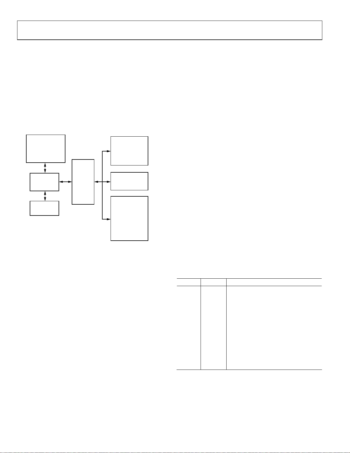
ADuC845/ADuC847/ADuC848
SPECIAL FUNCTION REGIST
The SFR space is mapped into the upper 128 bytes of internal
data memory space and accessed by direct addre
provides an inte face betwee
erals. A block diagra show
ADuC845/ADuC8 ADu
Figure 11.
All registers except the program counter (PC) and t
general- rpose re ster banks resi
isters in nt a registers that
reg clude co rol, configuration, and dat
provide an interface b erals.
62-kBYTE
ELECTRICALLY
REPROGRAMMABLE
NONVOLATILE
FLASH/EE PROGRAM
MEMORY
COMPATIBLE
256 BYTES RAM
2kBYTES XRAM
Accumulator SFR (ACC)
ACC is the accumulator register, which is used for math operations including addition, subtraction, integer multiplication and
division, and Boolean bit manipulations. The mnemonics for
accumulator-specific instructions usually refer to the
accumulator as A.
B SFR (B)
The B register is used with the accumulator for multiplication
and division operations. For other instructions, it can be treated
as a general-purpose scratch pad register.
r n the CPU and all on-chip periph-
m ing the programming model of the
47/ C848 via the SFR area is shown in
pu gi de in the SFR area. The SFR
etween the CPU and all on-chip periph
128-BYTE
8051-
CORE
SPECIAL
FUNCTION
REGISTER
AREA
Figure 11. Programming Model
ERS (SFRs)
ELECTRICALLY
REPROGRAMMABLE
NONVOLATILE
FLASH/EE DATA
MEMORY
OTHER ON-CHIP
PERIPHERALS
TEMPERATURE
CURRENT SOU
12-BIT DAC
SERIAL I/O
ssing only. It
he four
4-kBYTE
Σ-∆ ADC
SENSOR
RCES
WDT
PSM
TIC
PWM
04741-011
Data Pointer (DPTR)
The data pointer is made up o
f three 8-bit registers: DPP (page
byte), DPH (high byte), and DPL (low byte). These provide
memory addresses for internal code and data memory access.
The DPTR can be manipulated as a 16-bit register (DPTR =
DPH, DPL), although INC DPTR instructions automatically
carry over to DPP, or as three independent 8-bit registers (D
PP,
DPH, DPL).
The ADuC845/ADu 847/ADu
pointers. See the D Data
C C848 support dual data
ual Pointers section.
Stack Pointer (SP and SPH)
The SP SFR is the stack pointer, which is used to hold an
internal M add called the top
is nted be data is stored during P
executions. Although
RAM, the SP register i his
causes the stack to beg
As mentioned earlier, t ded 11-bit stack
po e th a bits needed to make up the 11-bit s
po the SBs of the SPH byte located at B7H. T
en SPH e EXSP (CFG84x.7) bit must be set;
othe the SPH R can be neither written to nor read fr
Pr (PSW)
Th FR contai s several bits that reflect the current
status of the CPU as li
SFR Address:
Power-On Default:
Bit Addressable:
RA ress of the stack. The SP register
increme fore USH and CALL
the stack can reside anywhere in on-chip
s initialized to 07H after a reset. T
in at location 08H.
he parts offer an exten
inter. Th ree extr tack
inter are three L o
able the SFR, th
rwise, SF om.
ogram Status Word
e PSW S n
sted in Table 5.
D0H
00H
Yes
able 5. PSW SFR Bit Designations
T
Bit No. Name Description
7 CY Carry Flag.
6 AC Auxiliary Carry Flag.
5 F0 General-Purpose Flag.
4, 3 RS1, RS0 Register Bank Select Bits.
RS1 RS0 Selected Bank
0 0 0
0 1 1
1 0 2
1 1 3
2 OV Overflow Flag.
1 F1 General-Purpose Flag.
0 P Parity Bit.
Rev. B | Page 24 of 108

ADuC845/ADuC847/ADuC848
Power Control Register (PCON)
The PCON SFR contains bits for power-saving options and
general-purpose status flags as listed in Table 6.
SFR Address: 87H
Power-On Default: 00H
Bit Addressable: No
Table 6. PCON SFR Bit Designations
Bit No. Name Description
7 SMOD Double UART Baud Rate.
0 = Normal, 1 = Double Baud Rate.
6 SERIPD
5 INT0PD INT0 Power-Down Interrupt Enable.
4 ALEOFF If set to 1, the ALE output is disabled.
3 GF1 General-Purpose Flag Bit.
2 GF0 General-Purpose Flag Bit.
1 PD
0 ----- Not Implemented. Write Don’t Care.
Serial Power-Down Interrupt Enable. If this
bit is set, a serial interrupt from either SPI
2
C can terminate the power-down
or I
mode.
If this bit is set, either a level (
negative-going transition (
INT0 pin terminates power-down mode.
Power-Down Mode Enable. If se
part enters power-down mode.
IT0 = 0) or a
IT0 = 1) on th
t to 1, the
e
ADuC845/ADuC847/ADuC848 Configuration Register
(CFG845/CFG847/CFG848)
The CFG845/C
FG847/CFG848 SFR contains the bits necessary
to configure the internal XRAM and the extended SP. By default,
it configures the user into 8051 mode, that is, extended SP, and
the internal XRAM are disabled. When using in a program, use
the part name only, that is, CFG845, CFG847, or CFG8
48.
SFR Address: AFH
Power-On Default: 00H
Bit Addressable: No
Table 7. CFG845/CFG847/CFG848 SFR Bit Designations
Bit No. Name Description
7 EXSP Extended SP Enable.
If this bit is set to 1, the stack rolls over
from SPH/SP = 00FFH to 0100H.
If this bit is cleared to 0, SPH SFR is
disabled and the stack rolls over from
SP = FFH to SP = 00H.
6 ---- Not Implemented. Write Don’t Care.
5 ---- Not Implemented. Write Don’t Care.
4 ---- Not Implemented. Write Don’t Care.
3 ---- Not Implemented. Write Don’t Care.
2 ---- Not Implemented. Write Don’t Care.
1 ---- Not Implemented. Write Don’t Care.
0 XRAMEN
If this bit is set to 1, the internal XRAM is
mapped into the lower 2 kbytes of the
external address space.
If this bit is cleared to 0, the internal XR
is accessible and up to 16 MB of external
data memory become available. See
Figure 8.
AM
Rev. B | Page 25 of 108

ADuC845/ADuC847/ADuC848
ADC CIRCUIT INFORMATION
The ADuC845 incorporates two 10-channel (8-channel on th
MQFP package) 24-bit Σ-∆ ADCs, while the ADuC847 and
ADuC848 each incorporate a single 10-channel (8-channel on
the MQFP package) 24-bit and 16-bit Σ-∆ ADC.
Each part also includes an on-chip programmable gain
amplifier and configurable buffering (neither is ava
ilable on the
auxiliary ADC on the ADuC845). The parts also incorporate
digital filtering intended for measuring wide dynamic range an
low frequency signals such as those in weigh-scale, strain-gage,
pressure transducer, or temperature measurement applicatio
The ADuC845/ADuC847/ADuC848 can be configured as four
or five (MQFP/LFCSP package) fully-differential input channel
or as eight or ten (MQFP/LFCSP package) pseudo differential
input channels referenced to AINCOM. The ADC on each part
(primary only on the ADuC845) can be fully buffered interna
and can be programmed for one of eight inp
±20 mV to ±2.56 V (V
× 1.024). Buffering the input channel
REF
ut ranges from
means that the part can handle significant source impedanc
on the selected analog input and that RC filtering (for noise
rejection or RFI reduction) can be placed on the analog inputs
If the ADC is used with internal buffering disabled
(ADC0CON1.7 = 1, ADC0CON1.6 = 0), these unbuffered
inputs provide a dynamic load to the driving source. Therefo
resistor/capacitor combinations on the inputs can cause dc gain
errors, depending on the output impedance of the source that is
driving the ADC in
puts.
Table 8 and Table 9 show the allowable external resistance/
capacitance values for unbuffered mode such that no gain error
at the 16-bit and 20-bit levels, respectiv
ely, is introduced. When
used with internal buffering enabled, it is recommended that a
e
ns.
lly,
es
re,
capacitor (10 nF to 100 nF) be placed on the input to the ADC
(usually as part of an antialiasing filter) to aid in noise
performance.
The input channels are intended to convert signals directly from
sensors without the need for external signal conditioning. With
internal buffering disabled (relevant bits set/cleared in
ADC0CON1), external buffering might be required.
d
When the internal buffer is enabled, it might be necessa
offset the negative input channel by +100 mV and to offset the
positive channel by −100 mV
if the reference range is AV
ry to
DD
.
This accounts for the restricted common-mode input range in
the buffer. Some circuits, for example, bridge circuits, are
tly suitable to use without having to offset where the
s
inheren
/2 and is not sufficiently
output voltage is balanced around
V
REF
large to encroach on the supply rails. Internal buffering is no
available
ADC (ADuC845 only) is fixed at a gain range of ±2
The ADCs use a Σ-Δ conversion technique to realize up t
on the auxiliary ADC (ADuC845 only). The auxiliary
.50 V.
o
t
24 bits on the ADuC845 and the ADuC847, and up to 16 bits on
.
the ADuC848 of no mis g codes performance (20 Hz update
rate, chop enabled). The Σ-Δ modulator converts the sampled
input signal into a digital pulse train whose duty cycle cont
the digital information. A sinc
(see Table 28) is then used to decimate the modulator output
data stream to give a valid da
able output rates. The signal chain has two modes of operation,
m
chop enabled and chop disabled. The
A
DCMODE register enables or disables the chopping scheme.
sin
3
programmable low-pass filter
ta conversion result at program-
bit in the
CHOP
ains
Table 8. Maximum Resistance for No 16-Bit Gain Error (Unbuffered Mode)
External Capacitance
Gain 0 pF 50 pF 100 pF 500 pF 1000 pF 5000 pF
1 111.3 kΩ 27.8 kΩ 16.7 kΩ 4.5 kΩ 2.58 kΩ 700 Ω
2 53.7 kΩ 13.5 kΩ 8.1 kΩ 2.2 kΩ 1.26 kΩ 360 Ω
4 25.4 kΩ 6.4 kΩ 3.9 kΩ 1.0 kΩ 600 Ω 170 Ω
8–128 10.7 kΩ 2.9 kΩ 1.7 kΩ 480 Ω 270 Ω 75 Ω
Table 9. Maximum Resistance for No 20-Bit Gain Error (Unbuffered Mode)
External Capacitance
Gain 0 pF 50 pF 100 pF 500 pF 1000 pF 5000 pF
1 84.9 kΩ 21.1 kΩ 12.5 kΩ 3.2 kΩ 1.77 kΩ 440 Ω
2 42.0 kΩ 10.4 kΩ 6.1 kΩ 1.6 kΩ 880 Ω 220 Ω
4 20.5 kΩ 5.0 kΩ 2.9 kΩ 790 Ω 430 Ω 110 Ω
8–128 8.8 kΩ 2.3 k Ω 1.3 k Ω 370 Ω 195 Ω 50 Ω
Rev. B | Page 26 of 108
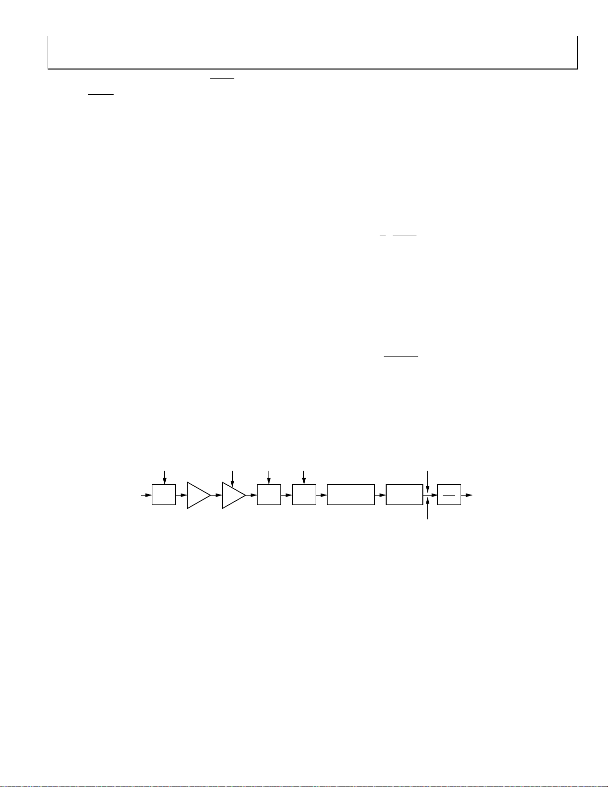
ADuC845/ADuC847/ADuC848
A
G
Signal Chain Overview (Chop Enabled,
With the
CHOP
bit = 0 (see the ADCMODE SFR bit designations in Table 24), the chopping scheme is enabled. This is the
default condition and gives optimum performance in terms of
offset errors and drift performance. With chop enabled, the
available output rates vary from 5.35 Hz to 105 Hz (SF = 255
and 13, respectively). A typical block diagram of the ADC input
channel with chop enabled is shown in Figure 12.
The sampling frequency of the modulator loop is many times
higher than the bandwidth of the input signal. The integrator in
the modulator shapes the quantization n
from the analog-to-digital conversion) so that the noise is pushe
toward one-half of the modulator frequency. The output of the
Σ-Δ modulator feeds directly into the digital filter. The digital
filter then band-limits the response to a frequency significantly
lower than one-half of the modulator frequency. In this manner,
the 1-bit output of the comparator is translated into a band
limited, low noise output from the ADCs.
3
The ADC filter is a low-pass Sinc
or (sinx/x)3 filter whose
primary function is to remove the quantization noise introduced
at the modulator. The cutoff frequency and decimated output
data rate of the filter are programmable via the Sinc filter word
loaded into the filter (SF) register (see Table 28). The complete
signal chain is chopped, resulting in excellent dc offset and
offset drift specifications and is extremely beneficial in applications where drift, noise rejection, and optimum EMI rejection
are important.
= 0)
CHOP
oise (which results
With
chop enabled, the ADC repeatedly reverses its inputs. The
deci
mated digital output words from the Sinc
have
a positive offset and a negative offset term included. As a
resu
lt, a final summing stage is included so that each output
word
from the filter is summed and averaged with the previous
filter
output to produce a new valid output result to be written
to th
e ADC data register. Programming the Sinc
3
filter, therefore,
3
decimation
factor is restricted to an 8-bit register called SF (see Table 28),
e actual decimation factor is the register value times 8.
th
Therefore, the decimated output rate from the Sinc
3
filter (and
the ADC conversion rate) is
d
1
f ×
SF
××=813
f
MODADC
where:
is the ADC conversion rate.
f
ADC
SF is the decimal equivalent of the word loaded to the filter
register.
is the modulator sampling rate of 32.768 kHz.
f
MOD
The chop rate of the channel is half the output data rate:
1
CHOP
As shown in the block diagram (Figure 12), the Sinc
outputs alternately contain +V
ff×=2
ADC
3
filter
and −VOS, where VOS is the
OS
respective channel offset.
NALO
INPUT
F
CHOP
MUX BUF
F
F
IN
MOD
Σ-∆
MOD
F
CHOP
XOR
SINC3 FILTERPGA 3 × (8 × SF)
t Channel with Chop Enabled Figure 12. Block Diagram of the ADC Inpu
F
ADC
AIN + V
AIN – V
Σ-∆
DIGITAL
2
OUTPUT
OS
OS
04741-013
Rev. B | Page 27 of 108
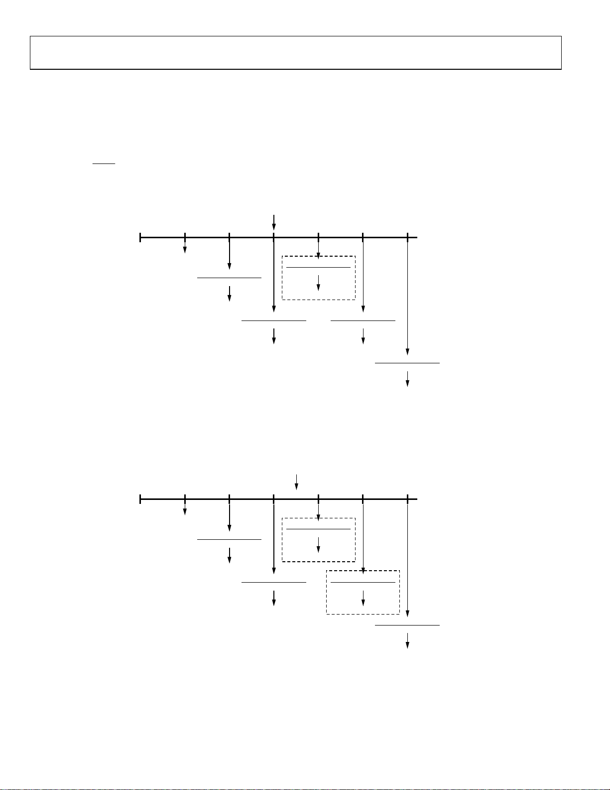
ADuC845/ADuC847/ADuC848
s offset i d by performing a r g avera 2.
Thi s remove unnin ge of
s average eans that the settling o any e in
Thi by 2 m time t chang
grammin e ADC is twice the no l conver time,
pro g of th rma sion
le an asy ous step change on th log inp ot
whi nchron e ana ut is n
reflecte he third subsequent t. See 13.
fully d until t outpu Figure
t ×== 2
SETTLE
f
2
ADC
t
ADC
SYNC
(I.E.
HRONOU NGE
S CHA
HANNEL GE)
CHAC N
e allowab nge for S op enab 13 to ith
Th le ra F (ch led) is 255 w
fault of espond nversi tes,
a de 69 (45H). The corr ing co on ra
nd pe eak no rforma are sho
rms a ak-to-p ise pe nces wn in
ble 10, Ta
Ta ble 11
cal and rated at a rential i oltage V
typi gene diffe nput v of 0
, Tabl e 1 nd Table he num are
2, a 13. T bers
and a common-mode voltage of 2.5 V. Note that the conversion time increases by 0.732 ms for each increment in
SF.
SAMPLE 1
NO/INVALID
SAMPLE 1
NO OUTPUT
SAMPLE 2 SAMPLE 3 SAMPLE 4 SAMPLE 5 SAMPLE 6
OUTPUT
SAMPLE 1 + SAMPLE 2
VALID OUTPUT
2
SAMPLE 2 + SAMPLE 3
VALID OU2TPUT
SAMPLE 3 + SAMPLE 4
2
NO OUTPUT
SAMPLE 4 + SAMPLE 5
VALID OUTP2UT
Figure 13. ADC Settling Time Following a Synchronous Change with
Chop Enabled
ASYNCH US CHA
RON
ISCONT US INPUT GE)
SAMPLE 2 SAMPLE 3 SAMPLE 4 SAMPLE 5 SAMPLE 6
SAMPLE 1 + SAMPLE 2
2
VALID OUTPUT
SAMPLE 2 + S
O NGE
INUO
SAMPLE 3 + SAMPLE 4
UNSETT2LED OUTPUT
AMPLE 3
2
CHAN(I.E. D
SAMPLE 4 + SAMPLE 5
2
SAMPLE 5 + SAMP
2
VALID OUTPUT
LE 6
04741-012
Figure 14. ADC Settlin
VALID OUTPUT
g Time Following an Asynchronous Change with
UNSETTLED OUTPUT
SAMPLE 5 + SAMPLE 6
VALID OUTPUT
2
04741-014
Chop Enabled
Rev. B | Page 28 of 108
ADuC845/ADuC847/ADuC848
ADC Noise Performance with Chop Enabled (
Table 10, Table 11, Table 12, and Table 13 show the output rm
noise and output peak-to-peak resolution in bits (rounded to
the nearest 0.5 LSB) for some typical output update rates for th
ADuC845, ADuC847, and ADuC848. The numbers are typica
and are generated at a differential input voltage of 0 V and a
common-mode voltage of 2.5 V. The output update rate is
selected via the SF7 to SF0 bits in the SF filter register. It is
important to note that the peak-to-peak resolution figures
represent the resolution for which there is no code flicker
within a 6-sigma limit.
The outp
the electrical noise in the semic uctor devices (device noise)
ut noise comes from two sources. The first source is
ond
Table 10. ADuC845 and ADuC847 Typical Output RMS Noise (µV) vs. Input Range and Update Rate with Chop Enabled
SF Word Data Update Rate (Hz) V ±640 mV ±1.28 V ±2.56 V ±20 mV ±40 mV ±80 mV ±160 mV ±320 m
13 105.03 1.75 1.30 1.65 1.5 2.1 3.1 7.15 13.3
23 59.36 1.25 0.95 1.08 0.94 1.0 1.87 3.24 7.1
27 50.56 1.0 1.0 0.85 0.85 1.13 1.56 2.9 3.6
69 19.79 0.63 0.68 0.52 0.7 0.61 1.1 1.3 2.75
255 5.35 0.31 0.38 0.34 0.32 0.4 0.45 0.68 1.22
Table 11. ADuC845 and ADuC847 Typical Peak-to-Peak Resolution (Bits) vs. Input Range and Update Rate with Chop Enabled
SF Word Data Update Rate (Hz) ±20 mV ±40 mV ±80 mV ±160 mV ±320 mV ±640 mV ±1.28 V ±2.56 V
13 105.03 12 13 14 15 15.5 16 16 16
23 59.36 12 13.5 14.5 15.5 16.5 16.5 17 16.5
27 50.56 12.5 13.5 15 16 16.5 17 17 17.5
69 19.79 13 14 15.5 16 17.5 17.5 18 18
255 5.35 14.5 15 16 17 18 18.5 19 19.5
Table 12. ADuC848 Typical Output Noise (µV) vs. Input Range and Update Rate with Chop Enabled
SF Word Data Update Rate (Hz) ±20 mV ±40 mV ±80 mV ±160 mV ±320 mV ±640 mV ±1.28 V ±2.56 V
13 105.03 1.75 1.30 1.65 1.5 2.1 3.1 7.15 13.3
23 59.36 1.25 0.95 1.08 0.94 1.0 1.87 3.24 7.1
27 50.56 1.0 1.0 0.85 0.85 1.13 1.56 2.9 3.6
69 19.79 0.63 0.68 0.52 0.7 0.61 1.1 1.3 2.75
255 5.35 0.31 0.38 0.34 0.32 0.4 0.45 0.68 1.22
Table 13. ADuC848 Typical Peak-to-Peak Resolution (Bits) vs. Input Range and Update Rate with Chop Enabled
SF Word Data Update Rate (Hz) ±20 mV ±40 mV ±80 mV ±160 mV ±320 mV ±640 mV ±1.28 V ±2.56 V
13 105.03 12 13 14 15 15.5 16 16 16
23 59.36 12 13.5 14.5 15.5 16 16 17 16
27 50.56 12.5 13.5 15 16 16 16 16 16
69 19.79 13 14 15.5 16 16 16 16 16
255 5.35 14.5 15 16 16 16 16 16 16
CHOP
= 0)
used in the implementation of the modulator. The second
s
source is quantization noise, which is added when the analog
input is converted to the digital domain. The device noise is at a
e
l
low level and is independent of frequency. The quantization
noise starts at an even lower level but rises rapidly with increasing
frequency to become the dominant noise source.
The numbers in the tables are given for the bipolar input ran
For the unipolar ran
ges, the rms noise numbers are in the same
ges.
range as the bipolar figures, but the peak-to-peak resolution is
based on half the signal range, which effectively means losing
1 bit of resolution.
Input Range
Input Range
Input Range
Input Range
Rev. B | Page 29 of 108

ADuC845/ADuC847/ADuC848
Signal Chain Overview with Chop Disabled (
With
= 1, chop is disabled and the available output rates
CHOP
vary from 16.06 Hz to 1.365 kHz. The range of applicable SF
words is from 3 to 255. When switching between channels with
chop disabled, the channel throughput rate is higher than wh
chop is enabled. The drawback with chop disabled is that the
drift performance is degraded and offset calibration is require
following a gain range change or significant temperature
change. A block diagram of the ADC input channel with chop
disable
d is shown in Figure 15.
The signal chain includes a multiplex or buffer, PGA, Σ-Δ
modulator, and digital filter. The modulator bit stream is
3
applied to a Sinc
ctor is restricted to an 8-bit register SF; the actual decimation
fa
filter. Programming the Sinc3 decimation
factor is the register value times 8. The decimated output rate
3
from the Sinc
f =
e:
wher
is the AD version rate.
f
ADC
the deci uivalent of th loade e filter
SF is
ter, valid ran rom 3 to 255.
regis
is the modulator sampling rate of 32.768 kHz.
f
D
MO
filter (and the ADC conversion rate) is therefore
1
SF×8
f×
MODADC
C con
mal eq
e word d to th
ge is f
CHOP
= 1)
en
d
The settling time to a step input is governed by the digital filte
A synchronized step change requires a settling time of three
r.
times the programmed update rate; a channel change can be
treated as a synchronized step change. This is one conversion
longer than the case for chop enabled. However, be
cause the
ADC throughput is three times faster with chop disabled than it
is with chop enabled, the actual time to a settled ADC output is
significantly less also. This means that following a synchronized
step change, the ADC requires three conversions (note: data is
not output following a synchronized ADC change until data h
as
settled) before the result accurately reflects the new input
voltage.
t ×== 3
SETTLE
f
3
ADC
t
ADC
An unsynchronized step change requires four conversions to
accur e new analog input at its output. Note that
ately reflect th
with an u ynchronize hange the C contin to outpu
data a the user t take un d output o accoun
Aga n with enable
bec ADC put w disa aster
with nable tual ti n to o sett
AD t is le
ns d c AD ues t
nd so mus settle s int t.
in, this is one conversion longer tha chop d, but
ause the through ith chop bled is f than
chop e d, the ac me take btain a led
C outpu ss.
The allowable range for SF is 3 to 255 with a default of 69 (45H).
The corresponding conversion rates, rms, and peak-to-peak
noise are shown in Table 14, Table 15, Table 16,
performances
and Tabl
for each
e 1 th n ti ases ms
7. Note that
incr SF.
ent in
em
e conversio me incre by 0.244
ANALOG
INPUT
F
IN
MUX BUF
Figure 15. Block Diagram of ADC Input Channel with Chop Disabled
F
MOD
Σ-∆
MOD
SINC3 FILTERPGA 8 × SF
F
ADC
DIGITAL
OUTPUT
04741-015
Rev. B | Page 30 of 108
 Loading...