

MicroConverter® Multichannel
24-/16-Bit ADCs with Embedded 62 kB
Flash and Single-Cycle MCU
FEATURES
High resolution Σ-∆ ADCs
2 independent 24-bit ADCs on the ADuC845
Single 24-bit ADC on the ADuC847 and
single 16-bit ADC on the ADuC848
Up to 10 ADC input channels on all parts
24-bit no missing codes
22-bit rms (19.5 bit p-p) effective resolution
Offset drift 10 nV/°C, gain drift 0.5 ppm/°C chop enabled
Memory
62-kbyte on-chip Flash/EE program memory
4-kbyte on-chip Flash/EE data memory
Flash/EE, 100-year retention, 100 kcycle endurance
3 levels of Flash/EE program memory security
In-circuit serial download (no external hardware)
High speed user download (5 sec)
2304 bytes on-chip data RAM
8051-based core
8051-compatible instruction set
High performance single-cycle core
32 kHz external crystal
On-chip programmable PLL (12.58 MHz max)
3 × 16-bit timer/counter
24 programmable I/O lines, plus 8 analog or
digital input lines
11 interrupt sources, two priority levels
Dual data pointer, extended 11-bit stack pointer
On-chip peripherals
Internal power-on reset circuit
12-bit voltage output DAC
Dual 16-bit Σ-∆ DACs
On-chip temperature sensor (ADuC845 only)
Dual excitation current sources (200 µA)
Time interval counter (wake-up/RTC timer)
UART, SPI®, and I
High speed dedicated baud rate generator (incl. 115,200)
Watchdog timer (WDT)
Power supply monitor (PSM)
2
C® serial I/O
ADuC845/ADuC847/ADuC848
Power
Normal: 4.8 mA max @ 3.6 V (core CLK = 1.57 MHz)
Power-down: 20 µA max with wake-up timer running
Specified for 3 V and 5 V operation
Package and temperature range:
52-lead MQFP (14 mm × 14 mm), −40°C to +125°C
56-lead LFCSP (8 mm × 8 mm), −40°C to +85°C
APPLICATIONS
Multichannel sensor monitoring
Industrial/environmental instrumentation
Weigh scales, pressure sensors, temperature monitoring
Portable instrumentation, battery-powered systems
Data logging, precision system monitoring
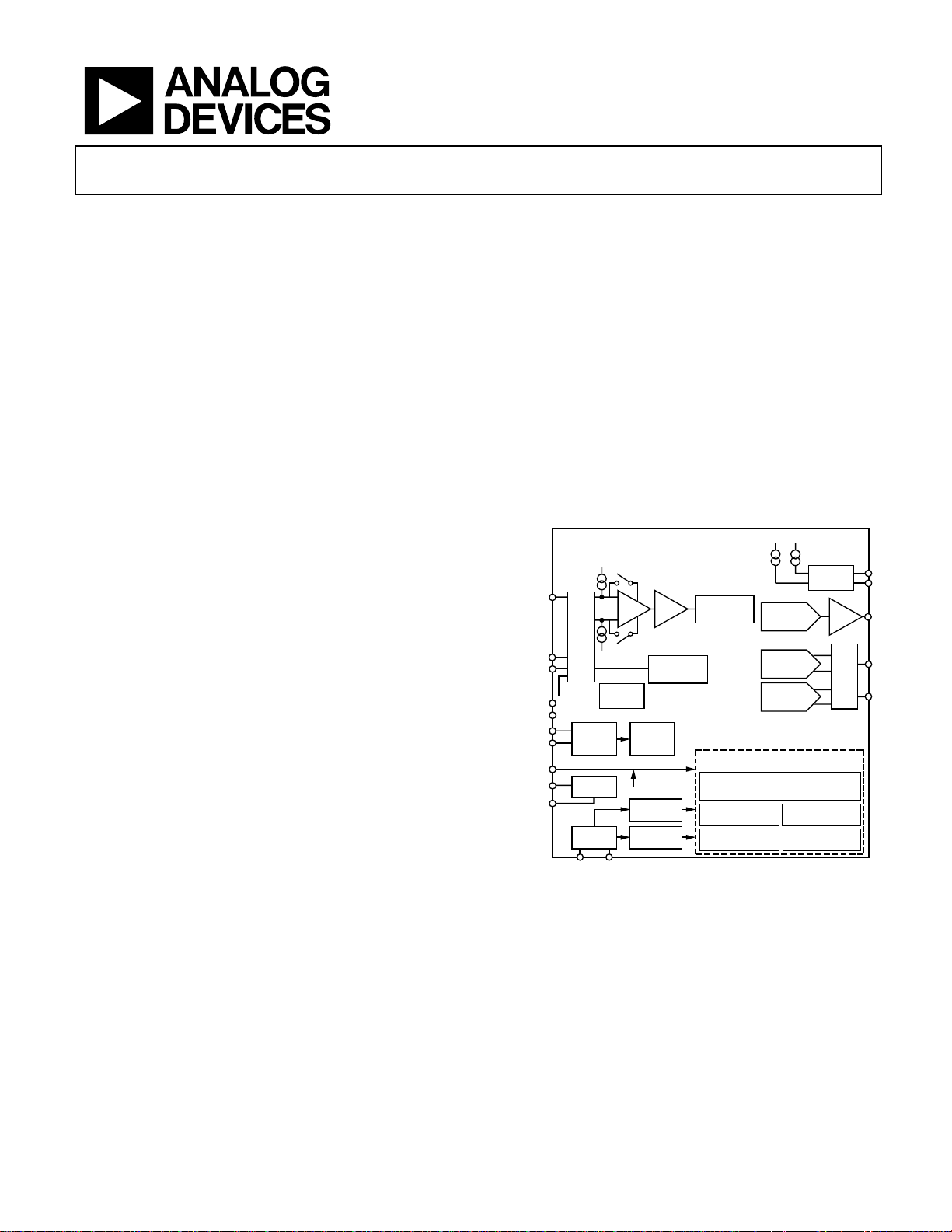
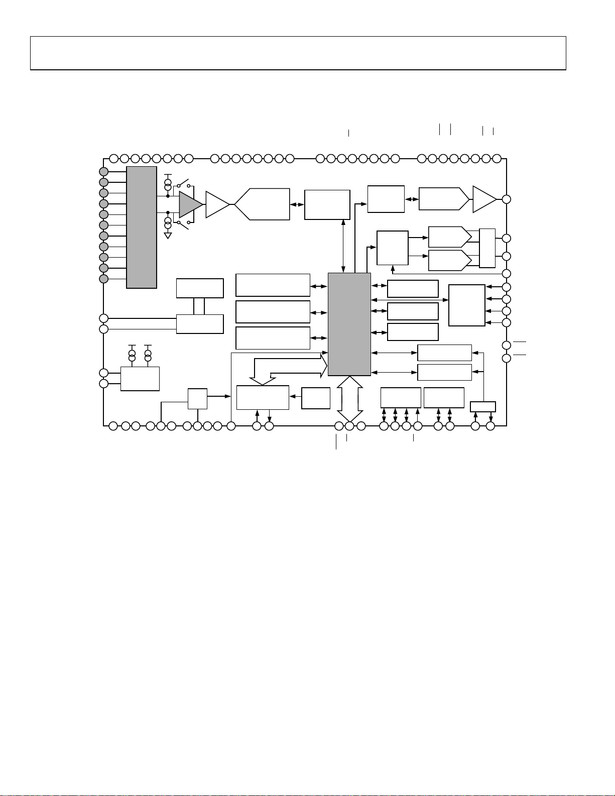
FUNCTIONAL BLOCK DIAGRAM
AV
DD
12-BIT
DAC
DUAL 16-BIT
Σ-∆ DAC
DUAL 16-BIT
PWM
POWER SUPPLY MON
WATCHDOG TIMER
UART, SPI, AND I
SERIAL I/O
CURRENT
SOURCE
BUF
MUX
2
C
AIN1
AIN10
AINCOM
REFIN2+
REFIN2–
REFIN–
REFIN+
RESET
DV
DGND
ADuC845
AVCO
PGABUF
MUX
AGND
TEMP
SENSOR
EXTERNAL
V
REF
DETECT
DD
POR
OSC
XTAL2XTAL1
AUXILIARY
24-BIT Σ-∆ ADC
INTERNAL
BAND GAP
V
REF
PLL AND PRG
CLOCK DIV
WAKE-UP/
RTC TIMER
PRIMARY
24-BIT Σ-∆ ADC
SINGLE-CYCLE 8061-BASED MCU
62 kBYTES FLASH/EE PROGRAM MEMORY
4 kBYTES FLASH/EE DATA MEMORY
2304 BYTES USER RAM
3 × 16 BIT TIMERS
BAUD RATE TIMER
4 × PARALLEL
PORTS
Figure 1. ADuC845 Functional Block Diagram
IEXC1
IEXC2
DAC
PWM0
PWM1
04741-001
Rev. B
Information furnished by Analog Devices is believed to be accurate and reliable.
However, no responsibility is assumed by Analog Devices for its use, nor for any
infringements of patents or other rights of third parties that may result from its use.
Specifications subject to change without notice. No license is granted by implication
or otherwise under any patent or patent rights of Analog Devices. Trademarks and
registered trademarks are the property of their respective owners.
One Technology Way, P.O. Box 9106, Norwood, MA 02062-9106, U.S.A.
Tel: 781.329.4700
Fax: 781.326.8703 © 2005 Analog Devices, Inc. All rights reserved.
www.analog.com

ADuC845/ADuC847/ADuC848
TABLE OF CONTENTS
Specifications..................................................................................... 4
ADC SFR Interface..................................................................... 39
Abosolute Maximum Ratings ....................................................... 10
ESD Caution................................................................................ 10
Pin Configurations and Function Descriptions .........................11
General Description ....................................................................... 15
8052 Instruction Set ...................................................................18
Timer Operation......................................................................... 18
ALE............................................................................................... 18
External Memory Access........................................................... 18
Complete SFR Map .................................................................... 19
Functional Description .................................................................. 20
8051 Instruction Set ...................................................................20
Memory Organization ............................................................... 22
Special Function Registers (SFRs)............................................ 24
ADC Circuit Information.......................................................... 26
Auxiliary ADC (ADuC845 Only) ............................................32
Reference Inputs......................................................................... 32
Burnout Current Sources ..........................................................32
Reference Detect Circuit ........................................................... 33
Sinc Filter Register (SF) .............................................................33
Σ-∆ Modulator ............................................................................ 33
Digital Filter ................................................................................33
ADC Chopping........................................................................... 34
Calibration................................................................................... 34
Programmable Gain Amplifier................................................. 35
Bipolar/Unipolar Configuration ..............................................35
Data Output Coding ..................................................................36
Excitation Currents ....................................................................36
ADC Power-On .......................................................................... 36
Typical Performance Characteristics........................................... 37
Functional Description .................................................................. 39
ADCSTAT (ADC Status Register) ........................................... 40
ADCMODE (ADC Mode Register)......................................... 41
ADC0CON1 (Primary ADC Control Register)..................... 43
ADC0CON2 (Primary ADC Channel Select Register) ........ 44
ADC1CON (Auxiliary ADC Control Register) (ADuC845
............................................................................................ 45
Only)
SF (ADC Sinc Filter Control Register) .................................... 46
ICON (Excitation Current Sources Control Register) .......... 47
Nonvolatile Flash/EE Memory Overview ............................... 48
Flash/EE Program Memory...................................................... 49
User Download Mode (ULOAD)............................................. 50
Using Flash/EE Data Memory .................................................. 51
Flash/EE Memory Timing ........................................................ 52
DAC Circuit Information .......................................................... 53
Pulse-Width Modulator (PWM).............................................. 55
On-Chip PLL (PLLCON).......................................................... 60
2
I
C Serial Interface ..................................................................... 61
SPI Serial Interface..................................................................... 64
Using the SPI Interface .............................................................. 66
Dual Data Pointers..................................................................... 67
Power Supply Monitor............................................................... 68
Watch d og T i mer ......................................................................... 69
Time Interval Counter (TIC).................................................... 70
8052-Compatible On-Chip Peripherals .................................. 73
Timers/Counters ........................................................................ 75
UART S er ia l I nte r f ac e ................................................................ 80
Interrupt System......................................................................... 85
Interrupt Priority........................................................................ 86
Interrupt Vectors........................................................................ 86
Hardware Design Considerations ................................................ 87
External Memory Interface ....................................................... 87
Rev. B | Page 2 of 108

ADuC845/ADuC847/ADuC848
Power Supplies.............................................................................87
QuickStart Development System..................................................94
Power-On Reset Operation........................................................88
Power Consumption ...................................................................88
Power-Saving Modes ..................................................................88
Grounding and Board Layout Recommendations .................89
Other Hardware Considerations...............................................90
REVISION HISTORY
2/05—Rev. A to Rev. B
Changes to Figure 1...........................................................................1
Changes to the Burnout Current Sources Section ......................32
Changes to the Excitation Currents Section................................36
Changes to Table 30 ........................................................................47
Changes to the Flash/EE Memory on the ADuC845, ADuC847,
ADuC848 Section......................................................................48
Changes to Figure 39 ......................................................................57
Changes to On-Chip PLL (PLLCON) Section............................60
Added 3 V Part Section Heading ..................................................88
Added 5 V Part Section ..................................................................88
Changes to Figure 70 ......................................................................91
Changes to Figure 71 ......................................................................93
6/04—Rev. 0 to Rev. A
Changes to Figure 5.........................................................................17
Changes to Figure 6.........................................................................18
Changes to Figure 7.........................................................................19
Changes to Table 5 ..........................................................................24
Changes to Table 24 ........................................................................41
QuickStart-PLUS Development System ..................................94
Timing Specifications .....................................................................95
Outline Dimensions......................................................................104
Ordering Guide.........................................................................105
Changes to Table 25........................................................................43
Changes to Table 26........................................................................44
Changes to Table 27........................................................................45
Changes to User Download Mode Section..................................50
Added Figure 51 and Renumbered Subsequent Figures............50
Edits to the DACH/DACL Data Registers Section..................... 53
Changes to Table 34........................................................................56
Added SPIDAT: SPI Data Register Section .................................65
Changes to Table 42........................................................................67
Changes to Table 43........................................................................68
Changes to Table 44........................................................................69
Changes to Table 45........................................................................71
Changes to Table 50........................................................................75
Changes to Timer/Counter 0 and 1 Data Registers Section...... 76
Changes to Table 54........................................................................80
Added the SBUF—UART Serial Port Data Register Section.....80
Addition to the Timer 3 Generated Baud Rates Section ...........83
Added Table 57 and Renumbered Subsequent Tables ...............84
Changes to Table 61........................................................................86
4/04—Revision 0: Initial Version
Rev. B | Page 3 of 108

ADuC845/ADuC847/ADuC848
SPECIFICATIONS
AVDD = 2.7 V to 3.6 V or 4.75 V to 5.25 V, DVDD = 2.7 V to 3.6 V or 4.75 V to 5.25 V, REFIN(+) = 2.5 V, REFIN(–) = AGND; AGND =
DGND = 0 V; XTAL1/XTAL2 = 32.768 kHz crystal; all specifications T
ADC, unless otherwise noted. Core speed = 1.57 MHz (default CD = 3), unless otherwise noted.
Table 1.
Parameter Min Typ Max Unit Conditions
PRIMARY ADC
Conversion Rate 5.4 105 Hz Chop on (ADCMODE.3 = 0)
16.06 1365 Hz Chop off (ADCMODE.3 = 1)
No Missing Codes
24 Bits ≤80.3 Hz update rate with chop disabled
Resolution (ADuC845/ADuC847) See Table 11 and Table 15
Resolution (ADuC848) See Table 13 and Table 17
Output Noise (ADuC845/ADuC847) See Table 10 and Table 14 µV (rms)
Output Noise (ADuC848) See Table 12 and Table 16 µV (rms)
Integral Nonlinearity ±15 ppm of FSR 1 LSB
Offset Error
Offset Error Drift vs. Temperature2 ±10 nV/°C Chop on (ADCMODE.3 = 0)
±200 nV/°C Chop off (ADCMODE.3 = 1)
Full-Scale Error
ADuC845/ADuC847 ±10 µV ±20 mV to ±2.56 V
ADuC848 ±10 µV ±20 mV to ±640 mV
±0.5 LSB
Gain Error Drift vs. Temperature
Power Supply Rejection
80 dB AIN = 1 V, ±2.56 V, chop enabled
113 dB AIN = 7.8 mV, ±20 mV, chop enabled
80 dB AIN = 1 V, ±2.56 V, chop disabled2
PRIMARY ADC ANALOG INPUTS
Differential Input Voltage Ranges
Bipolar Mode (ADC0CON1.5 = 0)
Unipolar Mode (ADC0CON1.5 = 1)
ADC Range Matching ±2 µV AIN = 18 mV, chop enabled
Common-Mode Rejection DC Chop enabled, chop disabled
On AIN 95 dB AIN = 7.8 mV, range = ±20 mV
113 dB AIN = 1 V, range = ±2.56 V
Common-Mode Rejection
50 Hz/60 Hz
On AIN 95 dB AIN = 7.8 mV, range = ±20 mV
90 dB AIN = 1 V, range = ±2.56 V
Footnotes at end of table.
3
4
2
1
to T
MIN
2
24 Bits ≤26.7 Hz update rate with chop enabled
±3 µV Chop on
4
±0.5 ppm/°C
, 5 6
Gain = 1 to 128
±1.024 ×
/GAIN
V
REF
0 – 1.024 ×
/GAIN
V
REF
V
V
, unless otherwise noted. Input buffer on for primary
MAX
Output noise varies with selected update rates,
gain range, and chop status.
Output noise varies with selected update rates,
gain range, and chop status.
16
Chop off, offset error is in the order of the noise
for the programmed gain and update rate
following a calibration.
16
±1.28 V to ±2.56 V
= REFIN(+) − REFIN(−) or
V
REF
REFIN2(+) − REFIN2(−) (or Int 1.25 V
= REFIN(+) − REFIN(−) or
V
REF
REFIN2(+) − REFIN2(−) (or Int 1.25 V
50 Hz/60 Hz ± 1 Hz, 16.6 Hz and 50 Hz update
rate, chop enabled, REJ60 enabled
REF
REF
)
)
Rev. B | Page 4 of 108

ADuC845/ADuC847/ADuC848
Parameter Min Typ Max Unit Conditions
Normal Mode Rejection 50 Hz/60 Hz
On AIN 75 dB
100 dB 50 Hz ± 1 Hz, 16.6 Hz Fadc, SF = 52H, chop on
67 dB
100 dB 50 Hz ± 1 Hz, 50 Hz Fadc, SF = 52H, chop off
Analog Input Current
2
±5 nA T
Analog Input Current Drift ±5 pA/°C T
±15 pA/°C T
Average Input Current ±125 nA/V ±2.56 V range, buffer bypassed
Average Input Current Drift ±2 pA/V/°C Buffer bypassed
Absolute AIN Voltage Limits
Absolute AIN Voltage Limits
EXTERNAL REFERENCE INPUTS
REFIN(+) to REFIN(–) Voltage 2.5 V REFIN refers to both REFIN and REFIN2
REFIN(+) to REFIN(–) Range
Average Reference Input Current ±1 µA/V Both ADCs enabled
Average Reference Input Current
Drift
NOXREF Trigger Voltage 0.3 0.65 V
Common-Mode Rejection
DC Rejection 125 dB AIN = 1 V, range = ±2.56 V
50 Hz/60 Hz Rejection
2
Normal Mode Rejection 50 Hz/60 Hz
67 dB
100 dB
AUXILIARY ADC (ADuC845 Only)
Conversion Rate 5.4 105 Hz Chop on
16.06 1365 Hz Chop off
No Missing Codes2 24 Bits ≤26.7 Hz update rate, chop enabled
24 Bits 80.3 Hz update rate, chop disabled
Resolution See Table 19 and Table 21
Output Noise See Table 18 and Table 20 Output noise varies with selected update rates.
Integral Nonlinearity ±15 ppm of FSR 1 LSB
Offset Error
3
±0.25 LSB
Offset Error Drift2 10 nV/°C Chop on
200 nV/°C Chop off
Full-Scale Error
Gain Error Drift
4
4
Power Supply Rejection 80 dB AIN = 1 V, range = ±2.56 V, chop enabled
80 dB AIN = 1 V, range = ±2.56 V, chop disabled
Footnotes at end of table.
2
50 Hz/60 Hz ± 1 Hz, 16.6 Hz Fadc, SF = 52H,
chop on, REJ60 on
50 Hz/60 Hz ± 1 Hz, 50 Hz Fadc, SF = 52H,
chop off, REJ60 on
±1 nA T
2
A
GND
0.1
2
A
GND
0.03
2
1 AV
+
−
±0.1
AV
0.1
AV
0.03
V AIN1…AIN10 and AINCOM with buffer enabled
−
DD
V AIN1…AIN10 and AINCOM with buffer bypassed
+
DD
V REFIN refers to both REFIN and REFIN2
DD
nA/V/°C
90 dB
= 85°C, buffer on
MAX
= 125°C, buffer on
MAX
= 85°C, buffer on
MAX
= 125°C, buffer on
MAX
NOXREF (ADCSTAT.4) bit active if V
inactive if V
> 0.65 V
REF
50 Hz/60 Hz ± 1 Hz, AIN = 1 V,
> 0.3 V, and
REF
range = ±2.56 V, SF = 82
2
75 dB
50 Hz/60 Hz ±1 Hz, AIN = 1 V, range = ±2.56 V,
SF = 52H, chop on, REJ60 on
100 dB
50 Hz ± 1 Hz, AIN = 1 V, range = ±2.56 V,
SF = 52H, chop on
50 Hz/60 Hz ± 1 Hz, AIN = 1 V, range = ±2.56 V,
SF = 52H, chop off, REJ60 on
50 Hz ± 1 Hz, AIN = 1 V, range = ±2.56 V,
SF = 52H, chop off
16
±3 µV Chop on
Chop off
±0.5 LSB
16
16
±0.5 ppm/°C
Rev. B | Page 5 of 108

ADuC845/ADuC847/ADuC848
Parameter Min Typ Max Unit Conditions
AUXILIARY ADC ANALOG INPUTS
(ADuC845 Only)
Differential Input Voltage Ranges
Bipolar Mode (ADC1CON.5 = 0) ±V
Unipolar Mode (ADC1CON.5 = 1) 0 – V
Average Analog Input Current 125 nA/V
Analog Input Current Drift ±2 pA/V/°C
Absolute AIN/AINCOM Voltage
Limits
Normal Mode Rejection 50 Hz/60 Hz
2, 7
On AIN and REFIN 75 dB
100 dB 50 Hz ± 1 Hz, 16.6 Hz Fadc, SF = 52H, chop on
67 dB
100 dB 50 Hz ± 1 Hz, 50 Hz Fadc, SF = 52H, chop off
ADC SYSTEM CALIBRATION
Full-Scale Calibration Limit +1.05 × FS V
Zero-Scale Calibration Limit −1.05 × FS V
Input Span 0.8 × FS 2.1 × FS V
DAC
Voltage Range 0 – V
0 – AV
Resistive Load 10 kΩ From DAC output to AGND
Capactive Load 100 pF From DAC output to AGND
Output Impedance 0.5 Ω
I
SINK
DC Specifications
8
Resolution 12 Bits
Relative Accuracy ±3 LSB
Differential Nonlinearity −1 LSB Guaranteed 12-bit monotonic
Offset Error ±50 mV
Gain Error ±1 % AVDD range
±1 % V
AC Specifications
2, 8
Voltage Output Settling Time 15 µs Settling time to 1 LSB of final value
Digital-to-Analog Glitch Energy 10 nVs 1 LSB change at major carry
INTERNAL REFERENCE
ADC Reference Chop enabled
Reference Voltage
Power Supply Rejection 45 dB
Reference Tempco 100 ppm/°C
DAC Reference
Reference Voltage 2.5 – 1% 2.5 2.5 + 1% ±1% V Initial tolerance @ 25°C, VDD = 5 V
Power Supply Rejection 50 dB
Reference Tempco ±100 ppm/°C
TEMPERATURE SENSOR
(ADuC845 Only)
Accuracy ±2 °C
Thermal Impedance 90 °C/W MQFP
52 °C/W LFCSP
Footnotes at end of table.
5, 6
REF
REF
−
A
GND
0.03
2
REF
DD
V REFIN = REFIN(+) − REFIN(−) (or Int 1.25 V
V REFIN = REFIN(+) − REFIN(−) (or Int 1.25 V
AVDD +
V
0.03
V DACCON.2 = 0
V DACCON.2 = 1
50 µA
1.25 − 1%
1.25 1.25 + 1% V Initial tolerance @ 25°C, VDD = 5 V
50 Hz/60 Hz ± 1 Hz, 16.6 Hz Fadc, SF = 52H,
chop on, REJ60 on
50 Hz/60 Hz ± 1 Hz, 50 Hz Fadc, SF = 52H,
chop off, REJ60 on
range
REF
REF
REF
)
)
Rev. B | Page 6 of 108

ADuC845/ADuC847/ADuC848
Parameter Min Typ Max Unit Conditions
TRANSDUCER BURNOUT CURRENT
SOURCES
AIN+ Current −100 nA
AIN− Current 100 nA
Initial Tolerance at 25°C ±10 %
Drift 0.03 %/°C
EXCITATION CURRENT SOURCES
Output Current 200 µA Available from each current source
Initial Tolerance at 25°C ±10 %
Drift 200 ppm/°C
Initial Current Matching at 25°C ±1 % Matching between both current sources
Drift Matching 20 ppm/°C
Line Regulation (AVDD) 1 µA/V AVDD = 5 V ± 5%
Load Regulation 0.1
Output Compliance
2
POWER SUPPLY MONITOR (PSM)
AVDD Trip Point Selection Range 2.63 4.63 V Four trip points selectable in this range
AVDD Trip Point Accuracy ±3.0 % T
±4.0 % T
DVDD Trip Point Selection Range 2.63 4.63 V Four trip points selectable in this range
DVDD Trip Point Accuracy ±3.0 % T
±4.0 % T
CRYSTAL OSCILLATOR
(XTAL1 AND XTAL2)
Logic Inputs, XTAL1 Only
V
, Input Low Voltage 0.8 V DVDD = 5 V
INL
2
0.4 V DVDD = 3 V
V
, Input Low Voltage 3.5 V DVDD = 5 V
INH
2.5 V DVDD = 3 V
XTAL1 Input Capacitance 18 pF
XTAL2 Output Capacitance 18 pF
LOGIC INPUTS
All inputs except SCLOCK, RESET,
and XTAL1
V
2
, Input Low Voltage 0.8 V DVDD = 5 V
INL
0.4 V DVDD = 3 V
V
, Input Low Voltage 2.0 V
INH
SCLOCK and RESET Only
(Schmidt Triggered Inputs)
V
T+
2
0.95 2.5 V DVDD = 3 V
V
T−
0.4 1.1 V DVDD = 3 V
VT+ − V
T−
Input Currents
Port 0, P1.0 to P1.7, EA
RESET ±10 µA VIN = 0 V, DVDD = 5 V
35 105 µA VIN = DVDD, DVDD = 5 V, internal pull-down
Port 2, Port 3 ±10 µA VIN = DVDD, DVDD = 5 V
−180 −660 µA VIN = 2 V, DVDD = 5 V
−20 −75 µA VIN = 0.45 V, DVDD = 5 V
Input Capacitance 10 pF All digital inputs
AIN+ is the selected positive input (AIN4 or AIN6
only) to the primary ADC
AIN− is the selected negative input (AIN5 or AIN7
only) to the primary ADC
MAX
MAX
MAX
MAX
= 85°C
= 125°C
= 85°C
= 125°C
AGND
AVDD − 0.6
µA/V
V
1.3 3.0 V DVDD = 5 V
0.8 1.4 V DVDD = 5 V
0.3 0.85 V DVDD = 5 V or 3 V
±10 µA V
= 0 V or V
IN
DD
Rev. B | Page 7 of 108

ADuC845/ADuC847/ADuC848
Parameter Min Typ Max Unit Conditions
LOGIC OUTPUTS
(All Digital Outputs except XTAL2)
VOH, Output High Voltage
2
2.4 V DVDD = 3 V, I
VOL, Output Low Voltage 0.4 V I
0.4 V I
Floating State Leakage Current
Floating State Output Capacitance 10 pF
START-UP TIME
At Power-On 600 ms
After Ext RESET in Normal Mode 3 ms
After WDT RESET in Normal Mode
From Power-Down Mode
Oscillator Running PLLCON.7 = 0
Wake-Up with INT0 Interrupt
Wake-Up with SPI Interrupt 20 µs
Wake-Up with TIC Interrupt 20 µs
Oscillator Powered Down PLLCON.7 = 1
Wake-Up with INT0 Interrupt
Wake-Up with SPI Interrupt 30 µs
FLASH/EE MEMORY RELIABILITY
CHARACTERISTICS
Endurance
Data Retention
9
10
POWER REQUIREMENTS
Power Supply Voltages
AVDD 3 V Nominal 2.7 3.6 V
AVDD 5 V Nominal 4.75 5.25 V
DVDD 3 V Nominal 2.7 3.6 V
DVDD 5 V Nominal 4.75 5.25 V
5 V Power Consumption 4.75 V < DVDD < 5.25 V, AVDD = 5.25 V
Normal Mode
11, 12
DVDD Current 10 mA Core clock = 1.57 MHz
25 31 mA Core clock = 12.58 MHz
AVDD Current 180 µA
Power-Down Mode
11, 12
DVDD Current 40 53 µA T
50 µA T
20 33 µA T
30 µA T
AVDD Current 1 µA T
3 µA T
Typical Additional Peripheral
Currents (AI
and DIDD)
DD
Primary ADC 1 mA
Auxiliary ADC (ADuC845 Only) 0.5 mA
Power Supply Monitor 30 µA
DAC 60 µA DACH/L = 000H
Dual Excitation Current Sources 200 µA
ALE Off −20 µA PCON.4 = 1 (see Table 6)
WDT 10 µA
Footnotes at end of table.
2.4 V DVDD = 5 V, I
= 8 mA, SCLOCK, SDATA
SINK
= 1.6 mA on P0, P1, P2
2
±10 µA
SINK
2 ms Controlled via WDCON SFR
20 µs
30 µs
100,000 Cycles
100 Years
= 85°C; OSC on; TIC on
MAX
= 125°C; OSC on; TIC on
MAX
= 85°C; OSC off
MAX
= 125°C; OSC off
MAX
= 85°C; OSC on or off
MAX
= 125°C; OSC on or off
MAX
5 V VDD, CD = 3
200 µA each. Can be combined to give 400 µA on
a single output.
SOURCE
SOURCE
= 80 µA
= 20 µA
Rev. B | Page 8 of 108

ADuC845/ADuC847/ADuC848
Parameter Min Typ Max Unit Conditions
PWM
−Fxtal 3 µA
−Fvco 0.5 mA
TIC 1 µA
3 V Power Consumption 2.7 V < DVDD < 3.6 V, AVDD = 3.6 V
Normal Mode
DVDD Current 4.8 mA Core clock = 1.57 MHz
9 11 mA Core clock = 6.29 MHz (CD = 1)
AVDD Current 180 µA ADC not enabled
Power-Down Mode
DVDD Current 20 26 µA T
29 µA T
14 20 µA T
21 µA T
AVDD Current 1 µA T
3 µA T
1
Temperature range is for ADuC845BS; for the ADuC847BS and ADuC848BS (MQFP package), the range is –40°C to +125°C.
Temperature range for ADuC845BCP, ADuC847BCP, and ADuC848BCP (LFCSP package) is –40°C to +85°C.
2
These numbers are not production tested but are guaranteed by design and/or characterization data on production release.
3
System zero-scale calibration can remove this error.
4
Gain error drift is a span drift. To calculate full-scale error drift, add the offset error drift to the gain error drift times the full-scale input.
5
In general terms, the bipolar input voltage range to the primary ADC is given by the ADC range = ±(V
V
= REFIN(+) to REFIN(–) voltage and V
REF
RN1, RN0 = 1, 1, 0, respectively, then the ADC range = ±1.28 V. In unipolar mode, the effective range is 0 V to 1.28 V in this example.
6
1.25 V is used as the reference voltage to the ADC when internal V
(AXREF is available only on the ADuC845.)
7
In bipolar mode, the auxiliary ADC can be driven only to a minimum of AGND – 30 mV as indicated by the auxiliary ADC absolute AIN voltage limits. The bipolar range
is still –V
8
DAC linearity and ac specifications are calculated using a reduced code range of 48 to 4095, 0 V to V
9
Endurance is qualified to 100 kcycle per JEDEC Std. 22 method A117 and measured at –40°C, +25°C, +85°C, and +125°C. Typical endurance at 25°C is 700 kcycles.
10
Retention lifetime equivalent at junction temperature (TJ) = 55°C per JEDEC Std. 22, Method A117. Retention lifetime based on an activation energy of 0.6 eV derates
with junction temperature.
11
Power supply current consumption is measured in normal mode following the power-on sequence, and in power-down modes under the following conditions:
REF
to +V
Normal mode: reset = 0.4 V, digital I/O pins = open circuit, Core Clk changed via CD bits in PLLCON, core executing internal software loop.
Power-down mode: reset = 0.4 V, all P0 pins and P1.2 to P1.7 pins = 0.4 V. All other digital I/O pins are open circuit, core Clk changed via CD bits in PLLCON, PCON.1 = 1,
core execution suspended in power-down mode, OSC turned on or off via OSC_PD bit (PLLCON.7) in PLLCON SFR.
12
DVDD power supply current increases typically by 3 mA (3 V operation) and 10 mA (5 V operation) during a Flash/EE memory program or erase cycle.
General Notes about Specifications
11, 12
11, 12
.
REF
RN
2
= 1.25 V when internal ADC V
REF
is selected. RN = decimal equivalent of RN2, RN1, RN0. For example, if V
REF
is selected via XREF0/XREF1 or AXREF bits in ADC0CON2 and ADC1CON, respectively.
REF
REF
, reduced code range of 100 to 3950, 0 V to VDD.
REF
= 85°C; OSC on; TIC on
MAX
= 125°C; OSC on; TIC on
MAX
= 85°C; OSC off
MAX
= 125°C; OSC off
MAX
= 85°C; OSC on or off
MAX
= 125°C; OSC on or off
MAX
)/1.25, where:
= 2.5 V and RN2,
REF
• DAC gain error is a measure of the span error of the DAC.
• The ADuC845BCP, ADuC847BCP, and ADuC848BCP (LFCSP package) have been qualified and tested with the base of the LFCSP
package floating. The base of the LFCSP package should be soldered to the board, but left floating electrically, to ensure good
mechanical stability.
• Flash/EE memory reliability characteristics apply to both the Flash/EE program memory and Flash/EE data memory.
Rev. B | Page 9 of 108

ADuC845/ADuC847/ADuC848
ABOSOLUTE MAXIMUM RATINGS
TA = 25°C, unless otherwise noted.
Table 2.
Parameter Rating
AVDD to AGND –0.3 V to +7 V
AVDD to DGND –0.3 V to +7 V
DVDD to DGND –0.3 V to +7 V
DVDD to DGND –0.3 V to +7 V
AGND to DGND
AVDD to DV
Analog Input Voltage to AGND
Reference Input Voltage to AGND –0.3 V to AVDD + 0.3 V
AIN/REFIN Current (Indefinite) 30 mA
Digital Input Voltage to DGND –0.3 V to DVDD + 0.3 V
Digital Output Voltage to DGND –0.3 V to DVDD + 0.3 V
Operating Temperature Range –40°C to +125°C
Storage Temperature Range –65°C to +150°C
Junction Temperature 150°C
θJA Thermal Impedance (MQFP) 90°C/W
θJA Thermal Impedance (LFCSP) 52°C/W
Lead Temperature, Soldering
Vapor Phase (60 sec) 215°C
Infrared (15 sec) 220°C
________________________
1
AGND and DGND are shorted internally on the ADuC845, ADuC847, and ADuC848.
2
Applies to the P1.0 to P1.7 pins operating in analog or digital input modes.
1
DD
2
–0.3 V to +0.3 V
–2 V to +5 V
–0.3 V to AVDD + 0.3 V
Stresses above those listed under Absolute Maximum Ratings
may cause permanent damage to the device. This is a stress
rating only; functional operation of the device at these or any
other conditions above those listed in the operational sections
of this specification is not implied. Exposure to absolute
maximum rating conditions for extended periods may affect
device reliability.
ESD CAUTION
ESD (electrostatic discharge) sensitive device. Electrostatic charges as high as 4000 V readily accumulate on
the human body and test equipment and can discharge without detection. Although this product features
proprietary ESD protection circuitry, permanent damage may occur on devices subjected to high energy
electrostatic discharges. Therefore, proper ESD precautions are recommended to avoid performance
degradation or loss of functionality.
Rev. B | Page 10 of 108
ADuC845/ADuC847/ADuC848
4
0
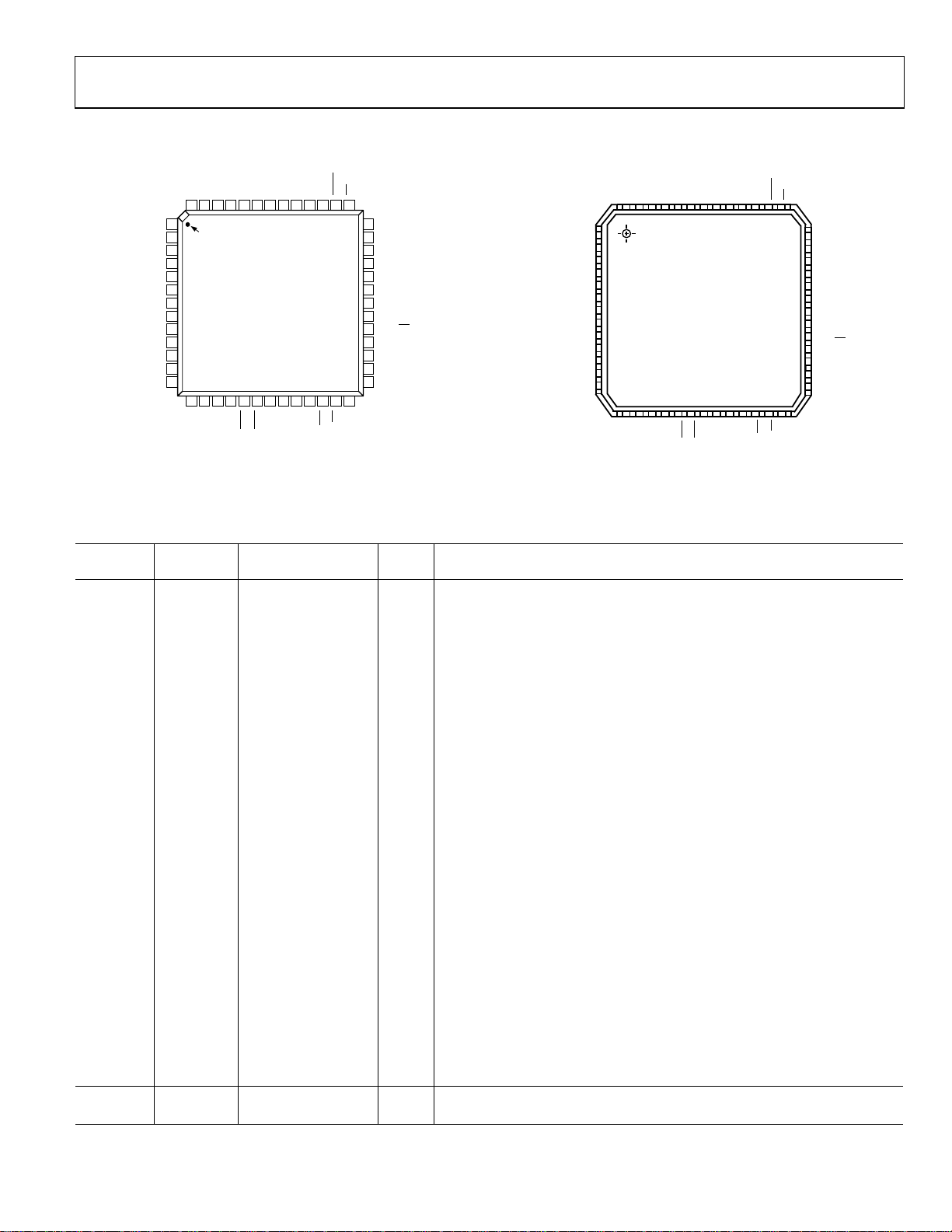
PIN CONFIGURATIONS AND FUNCTION DESCRIPTIONS
P0.6/AD6
54
RESET
P0.5/AD5
P0.4/AD4
52
53
TOP VIEW
(Notto Scale)
P3.1/TxD
P3.0/RxD
DD
DV
51
P3.2/INT0
DGND
50
P3.3/INT1
P0.3/AD3
49
DD
DV
P0.2/AD2
48
DGND
P0.1/AD1
47
P3.4/T0
P0.0/AD0
46
P3.5/T1
ALE
45
P3.6/WR
PSEN
44
P3.7/RD
EA
43
42
41
40
39
38
37
36
35
34
33
32
31
30
29
28
C)
2
SCLK (I
P1.0/AIN1
P1.1/AIN2
P1.2/AIN3/REFIN2+
P1.3/AIN4/REFIN2–
P1.6/AIN7/IEXC1
P1.7/AIN8/IEXC2
AV
AGND
REFIN–
REFIN+
P1.4/AIN5
P1.5/AIN6
AINCOM/DAC
P0.7/AD7P0.6/AD6P0.5/AD5P0.4/AD
52 51 50 49 48 43 42 41 4047 46 45 44
1
PIN 1
2
IDENTIFIER
3
4
5
DD
ADuC845/ADuC847/ADuC848
6
7
8
9
10
11
12
13
14 15 16 17 18 19 20 21 22 23 24 25 26
DAC
RESET
P3.0/RxD
DVDDDGND
TOP VIEW
(Not to Scale)
P3.1/TxD
P3.2/INT0
P3.3/INT1
P0.3/AD3P0.2/AD2P0.0/AD
DD
DV
P0.1/AD1
DGND
P3.4/T0
ALE
P3.5/T1
P3.6/WR
Figure 2. 52-Lead MQFP Pin Configuration
PSEN
EA
C)
2
P3.7/RD
SCLOCK (I
39
38
37
36
35
34
33
32
31
30
29
28
27
P2.7/PWMCLK
P2.6/PWM1
P2.5/PWM0
P2.4/T2EX
DGND
DV
DD
XTAL2
XTAL1
P2.3/SS/T2
P2.2/MISO
P2.1/MOSI
P2.0/SCLOCK (SPI)
SDATA
P1.0/AIN1
P0.7/AD7
55
56
AV
AGND
AGND
DAC
1
2
PIN 1
IDENTIFIER
3
4
DD
5
6
ADuC845/ADuC847/ADuC848
7
8
9
10
11
12
13
14
15161718192021222324252627
AIN9
AIN10
P1.1/AIN2
P1.2/AIN3/REFIN2+
P1.3/AIN4/REFIN2–
REFIN–
REFIN+
P1.4/AIN5
P1.5/AIN6
P1.6/AIN7/IEXC1
P1.7/AIN8/IEXC2
AINCOM/DAC
04741-002
Figure 3. 56-Lead LFCSP Pin Configuration
Table 3. Pin Fu
in No: Pin No: 56-
P
52-MQFP LFCSP Mnemonic
1 56 P1.0/AIN1 I B
nction Descriptions
Typ e
1
Description
y power-on default, P1.0/AIN1 is configured as the AIN1 analog input.
AIN1 can be u
sed as a pseudo differential input when used with AINCOM or as
the positive input of a fully differential pair when used with AIN2.
P1.0 has no digital output driver. It can function as a digital input for which 0
must be written to the port bit. As a digital input, this pin must be driven high
or low externally.
2 1 P1.1/AIN2 I
On power-on default, P1.1/AIN2 is configured as the AIN2 analog input.
AIN2 can be used as a pseudo differential input when used with AINCOM or as
the negative input of a fully differential pair when used with AIN1.
P1.1 has no digital output driver. It can function as a digital input for which 0
must be written to the port bit. As a digital input, this pin must be driven high
or low externally.
3 2 P1.2/AIN3/REFIN2+ I
On power-on default, P1.2/AIN3 is configured as the AIN3 analog input.
AIN3 can be used as a pseudo differential input when used with AINCOM or as
the positive input of a fully differential pair when used with AIN4.
P1.2 has no digital output driver. It can function as a digital input for which 0
must be written to the port bit. As a digital input, this pin must be driven high
or low externally. This pin also functions as a second external differential
reference input, positive terminal.
4 3 P1.3/AIN4/REFIN2− I
On power-on default, P1.3/AIN4 is configured as the AIN4 analog input.
AIN4 can be used as a pseudo differential input when used with AINCOM or as
the negative input of a fully differential pair when used with AIN3.
P1.3 has no digital output driver. It can function as a digital input for which 0
must be written to the port bit. As a digital input, this pin must be driven high
or low externally. This pin also functions as a second external differential
reference input, negative terminal.
5 4 AV
DD
S Analog Supply Voltage.
6 5 AGND S Analog Ground.
--- 6 AGND S A second analog ground is provided with the LFCSP version only.
7 7 REFIN− Reference Input, Negative Terminal. I External Differential
8 8 REFIN+ I External Differential Reference Input, Positive Terminal.
Footnotes at end of table.
P2.7/PWMCLK
P2.6/PWM1
P2.5/PWM0
P2.4/T2EX
DGND
DGND
DV
DD
XTAL2
XTAL1
P2.3/SS/T2
P2.2/MISO
P2.1/MOSI
P2.0/SCLOCK (SPI)
SDATA
04741-003
Rev. B | Page 11 of 108

ADuC845/ADuC847/ADuC848
Pin No:
52-MQFP
9 9 P1.4/AIN5 analog input.
10 10 P1.5/AIN6 I
11 11 P1.6/AIN7/IEXC1 I/O
12 12 P1.7/AIN8/IEXC2 I/O
13 13 AINCOM/DAC I/O
14 14 DAC O The voltage output from the DAC, if enabled, appears at this pin.
---- 15 AIN9 I
---- 16 AIN10
15 17 RESET I
16–
19
22–25
16 18 P3.0/RxD Receiver Data for UART Serial Port.
17 19 P3.1/TxD Transmitter Data for UART Serial Port.
18 20
19 21
22 24 P3.4/T0 Timer/Counter 0 External Input.
23 25 P3.5/T1 Timer/Counter 1 External Input.
24 26
25 27
Pin No: 56LFCSP
21
18–
24–27
Mnemonic
.7
P3.0–P3
INT0
P3.2/
INT1
P3.3/
WR
P3.6/
RD
P3.7/
Typ e
I On power-on default, P1.4/AIN5 is configured as the AIN5
I
I/O
r 0. External Interrupt 0. This pin can also be used as a gate control input to Time
External Interrupt 1. This pin can also be used as a gate control input to Timer 1.
1
Description
AIN5 can be used as a pseudo differential input when us
the positive input of a fully differential pair when used with AIN6.
P1.0 has no digital output driver. It can function as a digital input for whic
must be written to the port bit. As a digital input, this pin must be driven high
or low externally.
On power-on default, P1.5/AIN6 is configured as the AIN6 analog input.
AIN6 can be used as a pseudo differential input when used with AINCOM or as
the negative input
P1.1 has no digital output driver. It can function as a digital input for whic
must be written to the port bit. As a digital input, this pin must be driven high
or low externally.
On power-on default, P1.6/AIN7 is configured as the AIN7 analog input.
AIN7 can be used as a pseudo differential input when used with AINCOM or as
the positive input
current sources can also be configured at this pin.
P1.6 has no digital output driver. It can, however, function as a digital input for
which 0 must be written to the port bit. As a digital input, this pin must be
driven high or low externally.
On power-on default, P1.7/AIN8 is configured as the AIN8 analog input.
AIN8 can be used as a pseudo differential input when used with AINCOM or
the negative input of a fully dif
both current sources can also be configured at this pin.
P1.7 has no digital output driver. It can, however, function as a digital input for
which 0 must be written to the port bit. As a digital input, this pin must be
driven high or low externally.
All analog inputs can be referred to this pin, provided that a relevant pseudo
differential input mode is selected. This pin also functions as an alternative pin
out for the DAC.
AIN9 can be used as a pseudo differential analog input when used with
AINCOM or as the
AIN10 (LFCSP version only).
AIN10 can be used as a pseudo differential analog input when used with
AINCOM or as the negative input of a fully differential pair when used with
AIN9 (LFCSP version only).
Reset Input. A high level on this pin for 16 core clock cycles while the
oscillator is running resets the device. This pin has an internal weak pull-dow
and a Schmitt trigger input stage.
P3.0 to P3.7 are bidirectional port pins with internal pull-up resistors. P
pins that have 1s written to them are pulled high by the internal pull-up
resistors, and in that state can be used as inputs. As inputs, Port 3 pins being
pulled externally low source current because of the internal pull-up resistors
When driving a 0-to-1 output transition, a strong pull-up is active for one cor
clock period of the instruction cycle.
Port 3 pins also have the various secondary functions described below.
External Data Memory Write Strobe. This pin latches the data byte from Port 0
into an external data memory.
External Data Memory Read Strobe. This pin enables the data from an external
data memory to Port 0.
of a fully differential pair when used with AIN5.
of a fully differential pair when used with AIN8. One or both
ferential pair when used with AIN7. One or
positive input of a fully differential pair when used with
ed with AINCOM or as
ort 3
h 0
h 0
as
n
.
e
Rev. B | Page 12 of 108

ADuC845/ADuC847/ADuC848
Pin No:
52-MQFP
20, 34, 48
21, 35, 47
26 28 SCLK (I2C) I/O
27 29 SDATA I/O
28–31,
39
36– 42
28 30 P2.0/SCLOCK (SPI)
29 31 P2.1/MOSI
30 32 P2.2/MISO
31 33
36 39 P2.4/T2EX
37 40 P2.5/PWM0 0 output appears at this pin. If the PWM is enabled, the PWM
38 41 P2.6/PWM1 If the PWM is enabled, the PWM1 output appears at this pin.
39 42 P2.7/PWMCLK provided at this pin. If the PWM is enabled, an external PWM clock can be
32 34 XTAL1 I Input to the Crystal Oscillator Inverter.
33 35 XTAL2 O
40 43
41 44
42 45 ALE O
Pin No: 56LFCSP
22, 36, 51
7, 38, 50
23, 3
30–33, 39–
Mnemonic
DV
DD
DGND S Digital Ground.
Typ e
1
Description
S Digital Supply Voltage.
Serial Interface Clock for the I
triggered input. A weak
outputting logic
internal pull-up is present on this pin unless it is
low. This pin can also be controlled in software as a digital
2
C Interface. As an input, this pin is a Schmitt-
output pin.
2
Serial Data Pin for the I
C Interface. As an input, this pin has a weak intern
pull-up present unless it is outputting logic low.
P2.0–P2.7 I/O
Port 2 is a bid
irectional port with internal pull-up resistors. Port 2 pins that
have 1s written to them are pulled high by the internal pull-up resistors, and
in that state can be used as inputs. As inputs, Port
externally low source current because of the internal pull-up resistors. Port 2
emits the middle and high-order address bytes during accesses to the 24-bit
external data memory space.
Port 2 pins also have the various secondary functions described below.
Serial Interface Clock for the SPI Interface. As an input this pin is a Schmitt-
triggered input. A weak interna
outputting logic low.
Serial Master Output/Slave Input Data for the SPI Interface. A strong interna
pull-up is present on this pin when the SPI interface outputs a logic high.
strong internal pull-do
wn is present on this pin when the SPI interface
outputs a logic low.
Master Input/Slave Output for the SPI Interface. A weak pull-up is present on
this input pin.
P2.3/SS
/T2
Slave Select Input for the SPI
Interface. A weak pull-up is present on this pin.
For both package options, this pin can also be used to provide a clock input to
Timer 2. When e
nabled, Counter 2 is incremented in response to a negative
transition on the T2 input pin.
Control Input to Timer 2. When enabled, a negative transition on the T2EX
input pin causes a Timer 2 capture or reload event.
Output from the Crystal Oscillator Inverter. See the Hardware Desig
Considerations section for a description.
EA
External Access Enable, Logic Input. When held high, this input enables the
device to fetch code from internal program memory locations 0000H
F7FFH. No external program memory acce
ADuC847, or ADuC848. To determine the mode of code execution, the
is sampled at the end of an external RESET assertion or as part of a device
power cycle.
EA can also be used as an external emulation I/O pin, and
therefore the voltage level at this pin must not be changed during normal
operation because this might cause an emulation interrupt that halts code
execution.
PSEN
O
Program Store Enable, Logic Output. This function is not used on the
ADuC845, ADuC847, or ADuC848. This pin remains high during internal
program exe
cution.
PSEN can also be used to enable serial download mode when pulled lo
through a resistor at the end of an external RESET assertion or as part o
device power cycle.
Address Latch Enable, Logic Output. This output is used to latch the low by
(and page byte for 24-bit data address space accesses) of the address to
external memory dur
ing external data memory access cycles. It can be
disabled by setting the PCON.4 bit in the PCON SFR.
2 pins being pulled
l pull-up is present on this pin unless it is
n
to
ss is available on the ADuC845,
al
A
EA pin
w
f a
te
l
Rev. B | Page 13 of 108

ADuC845/ADuC847/ADuC848
Pin No:
52-MQFP
43–46,
49–52
1
I = input, O = output, S = supply.
Pin No: 56LFCSP
46–49, 52–
55
Mnemonic
P0.0–P0.7
Typ e
I/O
1
Description
These pins are part of Port 0, which is an 8-bit open-d
rain bidirectional I/O
port. Port 0 pins that have 1s written to them float, and, in that state, can be
used as high impedance inputs. An external pull-up resistor is required on P0
outputs to force a valid logic high level externally. Port 0 is also the
multiplexed low-order address and data bus during accesses to external data
memory. In this application, Port 0 uses strong internal pull-ups when
emitting 1s.
Rev. B | Page 14 of 108

ADuC845/ADuC847/ADuC848
GENERAL DESCRIPTION
The AD
12.58 M
ADuC836. They include additional analog inputs for
applications requiring more ADC channels.
The ADuC845, ADuC847, and ADuC848 are complete smar
transducer front ends. The family integrates high resolution
Σ-Δ ADCs with flexible, up to 10-channel, input multiplexing, a
f
sin
The ADuC845 includes two (primary and auxiliary) 24-bit Σ-Δ
ADCs with internal buffering and PGA on the primary ADC.
The ADuC847 includes the same primary ADC as the ADuC845
(auxiliary ADC removed). The ADuC848 is a 16-bit ADC
version of the ADuC847.
The ADCs incorporate flexible input multiplexing, a temperature
sensor (ADuC845 only), and a PGA (primary ADC only)
allowing direct measurement of low-level signals. The ADCs
include on-chip digital filtering and programmable output data
rates that are intended for measuring wide dynamic range and
low frequency signals, such as those in weigh scale, strain gage,
pressure transducer, or temperature measurement applications.
uC84 7, 848 are singl le,
5, ADuC84 and ADuC e-cyc
IPs, 8052 core upgr es to the ADuC834 and
ast 8-bit MCU, and program and data Flash/EE memory on a
gle chip.
ad
The devices operate from a 32 kHz crystal with an on-chip PL
generating a high frequency clock of 12.58 MHz. This clock is
routed through a programmable clock divider from which the
MCU core clock operating frequency is generated. The micro-
t
controller core is an optimized single-cycle 8052 offering
12.58 MIPs performance while maintaining 8051 instruction set
compatibility.
The available nonvolatile Flash/EE program memory options
are 62 kbytes, 32 kbytes, and 8 kbytes. 4 kbytes of nonvolatile
Flash/EE data memory and 2304 bytes of data RAM are also
provided on-chip. The program memory can be configured as
data memory to give up to 60 kbytes of NV data memory in
data logging applications.
On-chip factory firmware supports in-circuit serial download
and debug modes (via UART), as well as single-pin emulation
mode via the
are supported by the QuickStart™ development system featuring
low cost software and hardware development tools.
pin. The ADuC845, ADuC847, and ADuC848
EA
L
up to
Rev. B | Page 15 of 108
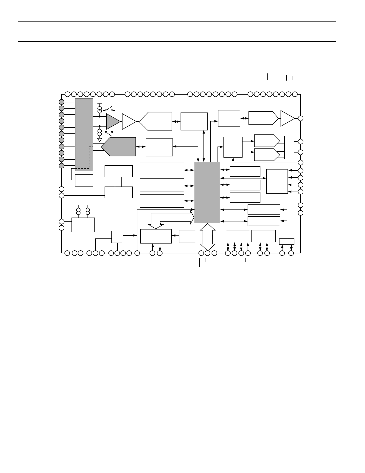
ADuC845/ADuC847/ADuC848
K
A
C
P0.0 (AD0)
P0.1 (AD1)
P0.2 (AD2)48P0.3 (AD3)49P0.4 (AD4)52P0.5 (AD5)53P0.6 (AD6)54P0.7 (AD7)
AIN1
AIN2
AIN3
AIN4
AIN5
AIN6
AIN7
AIN8
AIN9
AIN10
INCOM/DA
REFIN+
REFIN–
IEXC1
IEXC2
46 47
56
1
2
3
9
10
11
12
15
16
13
8
7
AIN
MUX
TEMP
SENSOR
200µA200µA
CURRENT
11
SOURCE
12
MIX
4 36 51 23 37 38 50 1817 19 44 43 45 30 31 32 33 28 29 34 35
5 6 22
DD
AV
AGND
NOTES
1. THE PIN NUMBERS REFER TO THE LFCSP PACKAGE ONLY.
BUF
AUXILIARY ADC
BAND GAP
REFERENCE
DD
DV
55
24-BIT
Σ-∆ ADC
V
REF
DETECT
POR
DGND
6)P2.0/SCLK (A8/A1
P1.0/AIN1
P1.1/AIN2
P1.2/AIN3/REFIN2+
56 1
P1.3/AIN4/REFIN2–3P1.4/AIN59P1.5/AIN610P1.6/AIN7/IEXC1
2
P1.7/AIN8/IEXC2
11
12
P2.1/MOSI (A9/A17)
P2.2/MISO (A10/A18)32P2.3/SS/T2 (A11/A19)33P2.4/T2EX (A12/A20)39P2.5/PWM0 (A13/A21)40P2.6/PWM1 (A14/A22)41P2.7/PWMCLK (A15/A23)
30 31
ADuC845
PGA
T
24-BI
Σ-∆ ADC
ADC
CONTR
AND
FLASH/EE
FLASH/EE
DOWDENLOADER
UART
TxD
RxD
C
NTERS
POINTER
BUGGER
PRIMARY AD
CALIBRATIOOLN
62 kBYTES PROGRAM/
4 kBYTES DATA/
2 × DATA POI
11-BIT STACK
SERIAL PORT
ESETR
ADC
C
ONTROL
AND
CA
LIBRATION
UART
TIMER
SINGLE-
CYCLE
8052
MCU
CORE
PSEN
Figure 4. Detailed Block Diagram of the ADuC845
EMULATOR
SINGLE-PIN
EA
CONTROL
ALE
42
DAC
PWM
CONTROL
2304 BYTES
USER RAM
WATCHDOG
TIMER
POWER SUPPLY
MONITOR
SPI SERIAL
INTERFACE
MOSI
SCLK
P3.0 (RxD)
P3.1 (TxD)
18 19
12-BIT
VOLTAGE
OUTPUT DAC
DUAL
16-BIT
Σ-∆ DAC
DUAL
16-BIT
PWM
PLL WITH PROG.
CLOCK DIVIDER
WAKE-UP/
RTC TIMER
I2C SERIAL
INTERFACE
SS
MISO
P3.2 (INT0)20P3.3 (INT1)21P3.4 (T0)24P3.5 (T1)25P3.6 (WR)26P3.7 (RD)
BUF
MUX
16-BIT
COUNTER
TIMERS
OSC
SCLK
SDATA
XTAL1
XTAL2
27
14
DAC
40
PWM0
41
PWM1
42
PWMCL
24
T0
25
T1
33
T2
39
T2EX
20
INT0
21
INT1
04741-004
Rev. B | Page 16 of 108
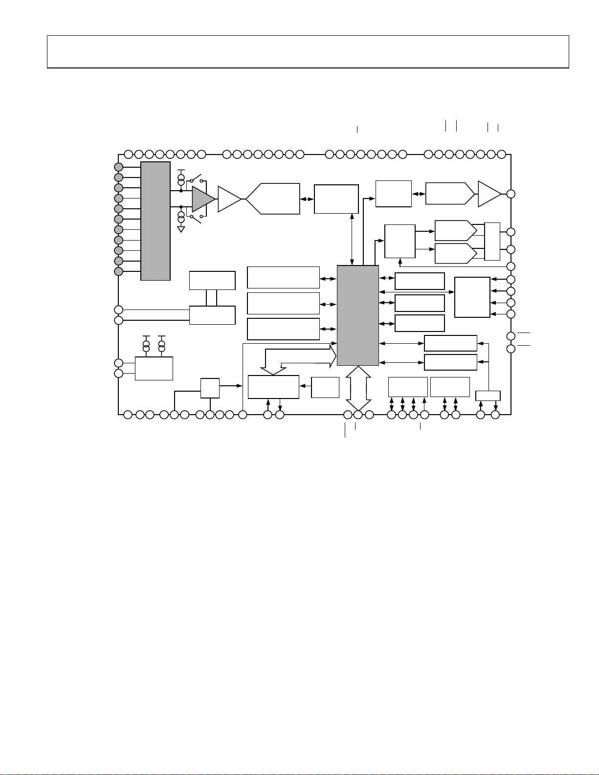
ADuC845/ADuC847/ADuC848
K
A
C
P0.0 (AD0)
P0.1 (AD1)
AIN1
AIN2
AIN3
AIN4
AIN5
AIN6
AIN7
AIN8
AIN9
AIN10
INCOM/DA
REFIN+
REFIN–
IEXC1
IEXC2
P0.2 (AD2)48P0.3 (AD3)49P0.4 (AD4)52P0.5 (AD5)53P0.6 (AD6)54P0.7 (AD7)
46 47
56
1
2
3
9
10
11
12
15
16
13
8
7
AIN
MUX
55
BUF
BAND GAP
REFERENCE
200µA200µA
CURRENT
11
SOURCE
12
MIX
4 36 51 23
5 6 22
DD
AV
AGND
NOTES
1. THE PIN NUMBERS REFER TO THE LFCSP PACKAGE ONLY.
DD
DV
P1.0/AIN1
P1.1/AIN2
P1.2/AIN3/REFIN2+
P1.3/AIN4/REFIN2–3P1.4/AIN59P1.5/AIN610P1.6/AIN7/IEXC1
2
PRIMARY ADC
24-BIT
Σ-∆ ADC
62 kBYTES PROGRAM/
FLASH/EE
4 kBYTES DATA/
FLASH/EE
2 × DATA POINTERS
11-BIT STACK POINTER
V
REF
DETECT
56 1
PGA
DOWNLOADER
POR
37 38 50 1817 19 44 43 45 30 31 32 33 28 29 34 35
DGND
UART
SERIAL PORT
RESET
RxD
Figure 5. Detailed Block Diagram of the ADuC847
P1.7/AIN8/IEXC212P2.0/SCLK (A8/A16)
11
ADuC847
DEBUGGER
TxD
P2.1/MOSI (A9/A17)
30 31
ADC
CONTROL
AND
CALIBRATION
SINGLE-
CYCLE
CORE
UART
TIMER
P2.2/MISO (A10/A18)32P2.3/SS/T2 (A11/A19)33P2.4/T2EX (A12/A20)39P2.5/PWM0 (A13/A21)40P2.6/PWM1 (A14/A22)41P2.7/PWMCLK (A15/A23)
DAC
CONTROL
PWM
CONTROL
8052
MCU
SINGLE-PIN
PSEN
EMULATOR
EA
ALE
POWER SUPPLY
SPI SERIAL
INTERFACE
SCLK
42
P3.0 (RxD)
18 19
OUTPUT DAC
2304 BYTES
USER RAM
WATCHDOG
TIMER
MONITOR
PLL WITH PROG.
CLOCK DIVIDER
SS
MOSI
MISO
P3.1 (TxD)
P3.2 (INT0)20P3.3 (INT1)21P3.4 (T0)24P3.5 (T1)25P3.6 (WR)26P3.7 (RD)
12-BIT
VOLTAGE
DUAL
16-BIT
Σ-∆ DAC
DUAL
16-BIT
PWM
16-BIT
COUNTER
TIMERS
WAKE-UP/
RTC TIMER
I2C SERIAL
INTERFACE
SCLK
SDATA
BUF
OSC
XTAL1
MUX
27
14
DAC
40
PWM0
41
PWM1
42
PWMCL
24
T0
25
T1
33
T2
39
T2EX
20
INT0
21
INT1
XTAL2
04741-070
Rev. B | Page 17 of 108
ADuC845/ADuC847/ADuC848
K
A
C
P0.0 (AD0)
P0.1 (AD1)
P0.2 (AD2)48P0.3 (AD3)49P0.4 (AD4)52P0.5 (AD5)53P0.6 (AD6)54P0.7 (AD7)
AIN1
AIN2
AIN3
AIN4
AIN5
AIN6
AIN7
AIN8
AIN9
AIN10
INCOM/DA
REFIN+
REFIN–
IEXC1
IEXC2
46 47
56
1
2
3
9
10
11
12
15
16
13
8
7
11
12
NOTES
1. THE PIN NUMBERS REFER TO THE LFCSP PACKAGE ONLY.
AIN
MUX
200µA200µA
CURRENT
SOURCE
MIX
4 36 51 23 37 38 50 1817 19 44 43 45 30 31 32 33 28 29 34 35
5 6 22
DD
AV
AGND
DD
DV
55
BUF
BAND GAP
REFERENCE
V
REF
DETECT
POR
DGND
P1.0/AIN1
P1.1/AIN2
P1.2/AIN3/REFIN2+
56 1
P1.3/AIN4/REFIN2–3P1.4/AIN59P1.5/AIN610P1.6/AIN7/IEXC1
2
P1.7/AIN8/IEXC212P2.0/SCLK (A8/A16)
11
P2.1/MOSI (A9/A17)
P2.2/MISO (A10/A18)32P2.3/SS/T2 (A11/A19)33P2.4/T2EX (A12/A20)39P2.5/PWM0 (A13/A21)40P2.6/PWM1 (A14/A22)41P2.7/PWMCLK (A15/A23)
30 31
ADuC848
PGA
11-BIT STACK POINTER
RESET
PRIMARY ADC
16-BIT
Σ-∆ ADC
62 kBYTES PROGRAM/
FLASH/EE
4 kBYTES DATA/
FLASH/EE
2 × DATA POINTERS
DOWNLOADER
DEBUGGER
UART
SERIAL PORT
TxD
RxD
ADC
CONTROL
AND
CALIBRATION
SINGLE-
CYCLE
UART
TIMER
8052
MCU
CORE
PSEN
Figure 6. Detailed Block Diagram of the ADuC848
EMULATOR
SINGLE-PIN
EA
CONTROL
ALE
42
DAC
PWM
CONTROL
2304 BYTES
USER RAM
WATCHDOG
TIMER
POWER SUPPLY
MONITOR
SPI SERIAL
INTERFACE
MOSI
SCLK
P3.0 (RxD)
P3.1 (TxD)
18 19
12-BIT
VOLTAGE
OUTPUT DAC
DUAL
16-BIT
Σ-∆ DAC
DUAL
16-BIT
PWM
PLL WITH PROG.
CLOCK DIVIDER
WAKE-UP/
RTC TIMER
I2C SERIAL
INTERFACE
SS
MISO
P3.2 (INT0)20P3.3 (INT1)21P3.4 (T0)24P3.5 (T1)25P3.6 (WR)26P3.7 (RD)
BUF
MUX
16-BIT
COUNTER
TIMERS
OSC
SCLK
XTAL1
SDATA
27
14
DAC
40
PWM0
41
PWM1
42
PWMCL
24
T0
25
T1
33
T2
39
T2EX
20
INT0
21
INT1
XTAL2
04741-072
8052 INSTRUCTION SET
Table 4 documents the number of clock cycles required for each
instruction. Most instructions are executed in one or two clock
cycles resulting in 12.58 MIPs peak performance when operating
at PLLCON = 00H.
TIMER OPERATION
Timers on a standard 8052 increment by one with each machine
ALE
On the ADuC834, the output on the ALE pin is a clock at 1/6th
of the core operating frequency. On the ADuC845, ADuC847,
and ADuC848, the ALE pin operates as follows. For a single
machine cycle instruction, ALE is high for the entire machine
cycle. For a two or more m
for the first machine cycle and then low for the remainder of the
machine cycles.
achine cycle instruction, ALE is high
cycle. On the ADuC845, ADuC847, and ADuC848, one
machine cycle is equal to one clock cycle; therefore, the timers
increment at the same rate as the core clock.
EXTERNAL MEMORY ACCESS
The ADuC845, ADuC847, and ADuC848 do not support
external program memory access, but the parts can access up to
16 MB (24 address bits) of external data memory. When
accessing external RAM, the EWAIT register might need to be
programmed in order to give extra machine cycles to MOVX
commands to allow for differing external RAM access speeds.
Rev. B | Page 18 of 108
ADuC845/ADuC847/ADuC848
COMPLETE SFR MAP
ISPI
WCOL
SPE
SPIM
CPO
CPHA
SPR1
FFH 0
FEH 0
FDH 0
FCH 0
FBHL0
FAH
1
F7H 0 F6H 0 F5H 0 F4H 0 F3H 0 F2H F1H 0 F0H 0
MDO
EFH 0 EEH 0
E7H 0 E6H 0 E5H 0 E4H 0 E3H 0 E2H E1H 0 E0H 0
RDY0
DFH 0
CY
D7H 0ACD6H 0F0D5H 0
TF2
CFH 0 CEH 0
PRE3
C7H 0 C6H
BFH 0 BEH 0
RD
B7H 1WRB6H 1T1B5H 1T0B4H 1
EA
AFH AEH
0
1
A7H A6H A5H 1 A4H 1 A3H 1 A2H A1H 1 A0H 1
SM0
9FH 0
97H 1 96H 1 95H 1 94H 1 93H 1 92H
TF1
8FH 0 8EH
87H 1 86H 1 85H 1 84H 1 83H 1 82H 81H 1 80H 1
MCO
MDE
RDY1
DEH 0
EXF2 RCLK
PRE20PRE1
PADC PT2
EADC ET2
00
1
SM1
9EH 0
TR10TF0
MDI
EDH 0 ECH 0 EBH 0 EAH E9H
CAL
NOXREF
DDH 0
DCH 0
DBH 0
RS1
D4H 0
D3H 0OVD2HFID1H 0PD0H 0
TCLK
CCH 0
PRE0
REN
9CH 0
TR0
8CH 0
EXEN2
CBH 0
C3H 0
BBH 0
B3H 1
ABH 0
9BH 0
8BH 0
CDH 0
C5H 0 C4H 1
BDH 0PSBCH 0
ADHESACH 0
SM2
9DH 0
8DH 0
I2CM
ERR0
RS0
WDIR
PT1
INT1
ET1
TB8
IE1
0
I2CRS I2CTX I2CI
0
0
ERR1
0
DAH D9H 0 D8H 0
0
TR2
0
CAH
WDS
0
C2H
PX1
0
BAH
INT0
B2H
1
EX1
0
AAH
1
RB8
9AHTI99H 0 98H 0
0
1
IT1
0
8AH
1
SPR0
F9H 0
F8H 0
0 E8H 0
CNT2
CAP2
C9H 0 C8H 0
WDE
WDWR
C1H 0 C0H 0
PT0
PX0
B9H 0
B8H 0
TxD
RxD
B1H 1
B0H 1
ET0
EX0
A9H 0
A8H 0
RI
T2EX
IE0
T2
90H 1
IT0
88H 0
91H 1
89H 0
BITS
BITS
BITS
BITS
BITS
BITS
BITS
BITS
BITS
BITS
BITS
BITS
BITS
BITS
BITS
BITS
SPICON
F8H 05H
RESERVED
B
F0H 00H
I2CCON
H 00H
E9H xxH EAH xxH EBH xxH ECH xxH EDHE8
ACC
E0H 00H
ADCSTAT
D8H 00H
E1H xxH
NOT AVAILABLE
PSW ADC
D0H 00H
C8H 00H
T2CON
D1H 08H
RESERVE
WDCON
C0H 10H
IP
B8H 00H
B9H 00H
P3
FFH
B0H
IE
A8H 00HIEA9H
P2
A0H FFH
A1H
SCON
00H98H
99H 00H
P1
90H FFH
TCON
88H 00H
89H 00H
P0
H FFH80
81H 07H
RESERVED
GN0L
OF0L
MODE
I2CADD1
F2H 7FH
2
GN0M2GN0H2GN1L2GN1
OF0M
E2H xxH
ADC0M
00HD9H
DAH 00H
ADC0C
D2H
RCAP2L
D
CAH 00H
HIPID
C
C2H A0H
RESERVED
RESERVED
ADC0L
ON ADuC848
RESERVED
ECON
PWM0L PWM0
B2H B3H
00H
IP2
A 0H
TIMECON
TMOD
HTHSEC
A2H A3H A4H
00H 00H 00H 00H
SBUF
I2CDAT
9AH 00H
TL0
8AH 00H
SP
DPL
82H 00H
DACL
FBH 00H
NOT USED
OF0H
E3H xxH
ADC0H
DBH 00H
ON1
ADC1CON
ADuC845 ONLY
07H
D3H 00HSFD4H 45H
RCAP2H
CBH 00H
RESERVED RESERVED
RESERVED
PWM1L PWM1H
H
00H
00H
1
1
SEC
I2CADD
9BH 55H
TL1
8BH 00H
DPH
83H 00H
DACH
DACCON
FCH 00H
ADuC845 ONLY ADuC845 ONLY
ADuC845 ONLY ADuC845 ONLY
E4H xxH
ADuC845 ONLY ADuC845 ONLY ADuC845 ONLY
DCH 00H
OF1L
ADC1M
FDH 00H
E5H
ADC
DDH 00H
D5H 00H
TL2
CCH 00H
EDATA1
BCH 00H
B4H
RESERVED
CDH 00H
RESER
EDAT
BDHA200H
00H
RESERRESERVEDRESERVEDRESERVED
1
MIN
HOU INTVA L
A5H
9DH 9EH 00H
TH0
8CH 00H
8DH 00H
DPP
84H 00H
RESERVED
RESVED ERVEDRESERRESERVED
2
H
RESERVED RESERVED
xxH
OF1
H
ADC0CON2
E6H 00H
xxH
ADC1L
1H
DEH 00H
ICON
RESERVED
TH2
RESERVED
EDARL
VED
C6H 00H
EDATA3
BEH 00H
RESERVEDRESERVED
PWMCON
VED
AEH
1
R
A6H H
00H
T3F T3CON
D
00H
TH1
RESERVED SERVED
RESERVEDRESER
VED
00H
00H
RESERVED
SPIDAT
F7H 00H
SERVED
RE
PSMCON
H DEH
DF
PLLCON
H 53H
D7
RESERVED
EDARH
H 00H
C7
DATA4
E
H 00H
BF
SPH
B7H
G845/7/8
CF
AFH
CON
DP
A7
AIT
EW
H 00H
9F
RESERVEDRESERVEDRESERVEDRESERVEDRESERVEDRESERVEDRESERVED
RE
PCON
H 00H
87
00HB1H
00H
00H
1
THESE SFR
2
CALIBRATION COEFFICIENTS ARE PRECONFIGURED ON POWER-UP TO FACTORY CALIBRATED VALUES.
s MAINTAIN THEIR PRE-RESET VALUES AFTER = 1.
R MAP KEY:
SF
A RESET IF TIMECON.0
THESE BITS ARE CONTAINED IN THIS BYTE.
BIT MNEMONIC
BIT ADDRESS
IE0
89H 0
IT0
88H 0
TCON
88H 00H
RESET DEFAULT BIT VALUE
NOTE:
SFR
s WHOSE ADDRESSES END IN 0H OR 8H ARE
SFR BIT ADDRESSABLE.
Figure 7. e ADuC845, ADuC847, and ADuC848
Complete SFR Map for th
MNEMONIC
RESET DEFAUL
SFR ADDRESS
T VALUE
04741-073
Rev. B | Page 19 of 108

ADuC845/ADuC847/ADuC848
FUNCTIO
8051
Table 4 tion Set
Mnemonic D B C
Arithmetic
A A,Rn Add register to A 1 1
ADD A,@Ri Add indirect memory to A 1 2
ADD A,dir Add direct byte to A 2 2
ADD A,#data Add immediate to A 2 2
ADDC A,Rn Add register to A with carry 1 1
ADDC A,@Ri Add indirect memory to A with carry 1 2
ADDC A,dir ith carry Add direct byte to A w 2 2
ADD A,#data Add immediate to A with carry 2 2
SUBB A,Rn Subtract register from A with borrow 1 1
SUBB A,@Ri Subtract indirect memory from A with borrow 1 2
SUBB A,dir Subtract direct from A with borrow 2 2
SUBB A,#data Subtract immediate from A with borrow 2 2
INC A Increment A 1 1
INC Rn Increment register 1 1
INC @Ri Increment indirect memory 1 2
INC dir Increment direct byte 2 2
INC DPTR Increment data pointer 1 3
DEC A Decrement A 1 1
DEC Rn Decrement register 1 1
DEC @Ri Decrement indirect memory 1 2
DEC dir Decrement direct byte 2 2
MUL AB Multiply A by B 1 4
DIV AB Divide A by B 1 9
DA A Decimal adjust A 1 2
Logic
ANL A,Rn AND register to A 1 1
ANL A,@Ri AND indirect memory to A 1 2
ANL A,dir AND direct byte to A 2 2
ANL A,#data iate to A AND immed 2 2
ANL dir,A AND A to direct byte 2 2
ANL dir,#data ediate data to direct byte AND imm 3 3
ORL A,Rn OR register to A 1 1
ORL A,@Ri to A OR indirect memory 1 2
ORL A,dir OR direct byte to A 2 2
ORL A,#data OR immediate to A 2 2
ORL dir,A OR A to direct byte 2 2
ORL dir,#data irect byte OR immediate data to d 3 3
XRL A,Rn Exclusive-OR register to A 1 1
XRL A,@Ri Exclusive-OR indirect memory to A 2 2
XRL A,#data Exclusive-OR immediate to A 2 2
XRL dir,A Exclusive-OR A to direct byte 2 2
XRL A,dir Exclusive-OR indirect memory to A 2 2
XRL dir,#data data to direct Exclusive-OR immediate 3 3
CLR A Clear A 1 1
CPL A Complement A 1 1
SWAP A Swap nibbles of A 1 1
RL A Rotate A left 1 1
NAL DESCRIPTION
INSTRUCTION SET
. Optimized Single-Cycle 8051 Instruc
escription ytes ycles
1
Rev. B | Page 20 of 108

ADuC845/ADuC847/ADuC848
Mnemonic Description Bytes Cycles
RLC A Rotate A left through carry 1 1
RR A Rotate A right 1 1
RRC A Rotate A right through carry 1 1
Data Transfer
MOV A,Rn Move register to A 1 1
MOV A,@Ri Move indirect memory to A 1 2
MOV Rn,A Move A to register 1 1
MOV @Ri,A Move A to indirect memory 1 2
MOV A,dir Move direct byte to A 2 2
MOV A,#data Move immediate to A 2 2
MOV Rn,#data Move register to immediate 2 2
MOV dir,A Move A to direct byte 2 2
MOV Rn, dir Move register to direct byte 2 2
MOV dir, Rn Move direct to register 2 2
MOV @Ri,#data Move immediate to indirect memory 2 2
MOV dir,@Ri Move indirect to direct memory 2
MOV @Ri,dir Move direct to indirect memory 2 2
MOV dir,dir te to direct byte Move direct by 3 3
MOV dir,#data Move immediate to direct byte 3 3
MOV DPTR,#data Move immediate to data pointer 3 3
MOVC A,@A+DPTR Move code byte relative DPTR to A 1 4
MOVC A,@A+PC Move code byte relative PC to A 1 4
MOVX2 A,@Ri Move external (A8) data to 1 4 A
MOVX2 A,@DPTR Move external (A16) data t 1 4 o A
MOVX2 @Ri,A Move A to external data (A8) 1 4
MOVX2 @DPTR,A Move A to external data (A16) 1 4
PU dir Push direct byteSH onto stack 2 2
POP dir Pop direct byte from stack 2 2
XCH Exchange A and register 1 1 A,Rn
XC A,@Ri ExH change A and indirect memory 1 2
XC D A,@Ri H Exchange A and indirect memory nibble 1 2
XCH A Exchange A and direct by,dir te 2 2
Boolean
CLR C Clear carry 1 1
CLR bit Clear direct bit 2 2
SETB C Set carry 1 1
SETB bit Set direct bit 2 2
CPL C Complement carry 1 1
CPL bit Complement direct bit 2 2
ANL C,bit AND direct bit and carry 2 2
ANL C,/bit AND direct bit inverse to carry 2 2
ORL C,bit OR direct bit and carry 2 2
ORL C,/bit OR direct bit inverse to carry 2 2
MOV C,bit Move direct bit to carry 2 2
MOV bit,C Move carry to direct bit 2 2
Branching
JMP @A+DPTR Jump indirect relative to DPTR 1 3
RET Return from subroutine 1 4
RETI Return from interrupt 1 4
ACALL addr11 Absolute jump to subroutine 2 3
AJMP addr11 Absolute jump unconditional 2 3
Footnotes at end of table.
2
1
Rev. B | Page 21 of 108

ADuC845/ADuC847/ADuC848
Mnemoni ption c Descri Bytes Cycles
SJMP rel Short jump (relative address) 2 3
JC rel Jump on carry = 1 3 2
JNC rel Jump on carry = 0 2 3
JZ rel Jump on accumulator = 0 2 3
JNZ rel Jump on accumulator ! = 0 2 3
DJNZ Rn,rel Decrement register, JNZ relative 2 3
LJMP Long jump unconditional 3 4
LCALL3 addr16 Long jump to subroutine 3 4
JB bit,rel Jump on direct bit = 1 3 4
JNB bit,rel Jump on direct bit = 0 4 3
JBC bit,rel Jump on direct bit = 1 and clear 3 4
CJNE A,dir,rel Compare A, direct JNE rela 4 tive 3
CJNE A,#data,rel Compare A, immediate JNE relative 3 4
CJNE Rn,#data,rel Compare register, immediate JNE relative 3 4
CJNE @Ri,#data,rel Compare indirect, immediate JNE relative 3 4
DJNZ dir,rel Decrement direct byte, JNZ relative 3 4
Miscellaneous
NOP No operation 1 1
1
1
One cycle is one clock.
2
MOVX instructions are four cycles when they have 0 wait state. Cycles of MOVX instructio AIT.
3
LCALL instructions are three cycles when the LCALL instruction comes from an interrupt.
MEMORY ORGANIZATION
The ADuC845, ADuC847, and ADuC848 contain four memory
blocks:
• 62 kbytes/3 h/EE program
memory
• 4 kbytes of on-chip Flash/EE data memory
• 256 bytes of general-purpose RAM
• 2 kbytes of internal XRAM
Flash/EE Program Memory
The parts provide up to 62 kbytes of Flash/EE program memory
to run user code. All further references to Flash/EE program
2 kbytes/8 kbytes of on-chip Flas
ns are 4 + n cycles when they have n wait states as programmed via EW
Flash/EE Data Memory
The user has 4 kbytes of Flash/EE data memory available that
can be accessed indirectly by using a group of registers mapped
into the sp
the Nonvola
General-Purp e
The general-purpos AM i
memories, the upp nd th
lower 128 bytes of RAM can be accessed through direct or
ecial function register (SFR) space. For details, see
tile Flash/EE Memory Overview section.
os RAM
e R s divided into two separate
er a e lower 128 bytes of RAM. The
indirect addressing. The upper 128 bytes of RAM can be
accessed only through indirect addressing because it shares th
same address space as the SFR space, which must be accessed
through direct addressing.
e
memory assume the 62-kbyte option.
The lower 128 bytes of internal data memory are mapped as
When
hardware reset, the parts default to code execution from their
internal 62 kbytes of Flash/EE program memory. The parts do
not support the rollover from internal code space to external
code space. No external code space is available on the parts.
Permanently embedded firmware allows code to be serially
downloaded to the 62 kbytes of internal code space via the
UART serial port while the device is in-circuit. No external
hardware is required.
During run time, 56 kbytes of the 62-kbyte program memory
can be reprogrammed. This means that the code space can be
upgraded in the field by using a user-defined protocol running
on the parts, or it can be used as a data memory. For details, see
is pulled high externally during a power cycle or a
EA
shown in Figure 8. The lowest 32 bytes are grouped into four
banks of eight registers addressed as R0 to R7. The next 16 bytes
(128 bits), locations 20H to 2FH above the register banks, form
a block of directly addressable bit locations at Bit Addresses
00H to 7FH. The stack can be located anywhere in the internal
memory address space, and the stack depth can be expanded up
to 2048 bytes.
Reset initializes the stack pointer to location 07H. Any call or
push pre-increments the SP before loading the stack. Therefore,
loading the stack starts from location 08H, which is also the
first register (R0) of Register Bank 1. Thus, if one is going to use
more than one register bank, the stack pointer should be
initialized to an area of RAM not used for data storage.
the Nonvolatile Flash/EE Memory Overview section.
Rev. B | Page 22 of 108
ADuC845/ADuC847/ADuC848
7FH
GENERAL-PURPOSE
AREA
30H
2FH
BANKS
SELECTED
VIA
BITS IN PSW
20H
11
18H
10
10H
01
08H
00
00H
1FH
17H
0FH
07H
BIT-ADDRESSABLE
(BIT ADDRESSES)
FOUR BANKS OF EIGHT
REGISTERS
R0 TO R7
RESET VALUE OF
STACK POINTER
04741-008
Figure 8. Lower 128 Bytes of Internal Data Memory
Internal XRAM
The ADuC845, ADuC847, and ADuC848 contain 2 kbytes of
on-chip extended data memory. This memory, although onchip, is accessed via the MOVX instruction. The 2 kbytes of
internal XRAM are mapped into the bottom 2 kbytes of the
external address space if the CFG84x.0 (Table 7) bit is set;
otherwise, access to the external data memory occurs just like a
standard 8051.
Even with the CFG84x.0 bit set, access to the external (off chip),
XRAM occurs once the 24-bit DPTR is greater than 0007FFH.
FFFFFFH
EXTERNAL
DATA
MEMORY
SPACE
(24-BIT
ADSPDRESS
ACE)
FFFFFFH
EXTERNAL
DATA
MEMORY
SPACE
(24-BIT
ADDRESS
SPACE)
is possible (by setting C
enable the 11-bit extended stack pointer. In this case, the stack
rolls over from FFH in RAM to 0100H in XRAM.
The 11-bit stack pointer is visible in the SPH and SP SFRs. Th
SP SFR is located at 81H as with a standard 8052. The SPH SF
is located at B7H. The 3 LSBs of the SPH SFR contain the 3
extra bits nece
ssary to extend the 8-bit stack pointer in the SP
SFR into an 11-bit stack pointer.
CFG845/7/8.7 = 0
FFH
00H
Figure 10. Extended Stack Pointer Operation
External Data Memory (External XRAM)
There is no support for external progra
parts. Howeve ju
r, st like a standard 8051-compatible core, the
ADuC845/ADuC847/ADuC
memory using a M X ins
utomatically outputs the various control strobes required to
a
access the data memory. The parts, ho
16 Mbytes of external data memory. T
the 64 kb tes of ext al data memor
sta ible core. Se
Co tions for details.
y ern y space available on a
ndard 8051-compat e the Hardware Design
nsidera section
FG845.7/ADuC847.7/ADuC848.7) to
07FFH
UPPER 1792
BYTES OF
ON-CHIP XRAM
(DATA + STACK
FOR EXSP = 1,
DATA ONLY
FOR EXSP = 0)
CFG845/7/8.7 = 1
100H
256 BYTES OF
ON-CHIP DATA
RAM
(DATA +
STACK)
ON-CHIP XRAM
(DATA ONLY)
00H
LOWER 256
BYTES OF
04741-010
m memory access to the
848 can access external data
OV truction. The MOVX instruction
wever, can access up to
his is an enhancement of
e
R
000800H
000000H
0007FFH
000000H
CFG845/7/8.0 = 0
2 kBYTES
ON-CHIP
XRAM
CFG845/7/8.0 = 1
04741-009
Figure 9. Internal and External XRAM
When enabled and when accessing the internal XRAM, the P0
and P2 port pin operations, as well as the
and WR strobes,
RD
do not operate as a standard 8051 MOVX instruction. This
allows the user to use these port pins as standard I/O. The
internal XRAM can be configured as part of the extended 11-bit
stack pointer. By default, the stack operates exactly like an 8052
in that it rolls over from FFH to 00H in the general-purpose
RAM. On the ADuC845, ADuC847, and ADuC848, however, it
Rev. B | Page 23 of 108
acce rn ter might need
When ssing exte al RAM, the EWAIT regis
be prog mmed to g xt chin OVX
to ra ive e ra ma e cycles to the M
peration. This is to account differi external RAM access
o for ng
peeds.
s
AIT SFR
EW
R Address:
SF
wer-On ult:
Po
ddres e:
Bit A sabl No
This s
Defa
9FH
00H
pecial function register (SFR), when programmed,
dictates the number of wait states for the MOVX instruction.
The value can vary between 0H and 7H. The MOVX instruction increases by one machine cycle (4 + n, where n = EWAIT
number in decimal) for every increase in the EWAIT value.
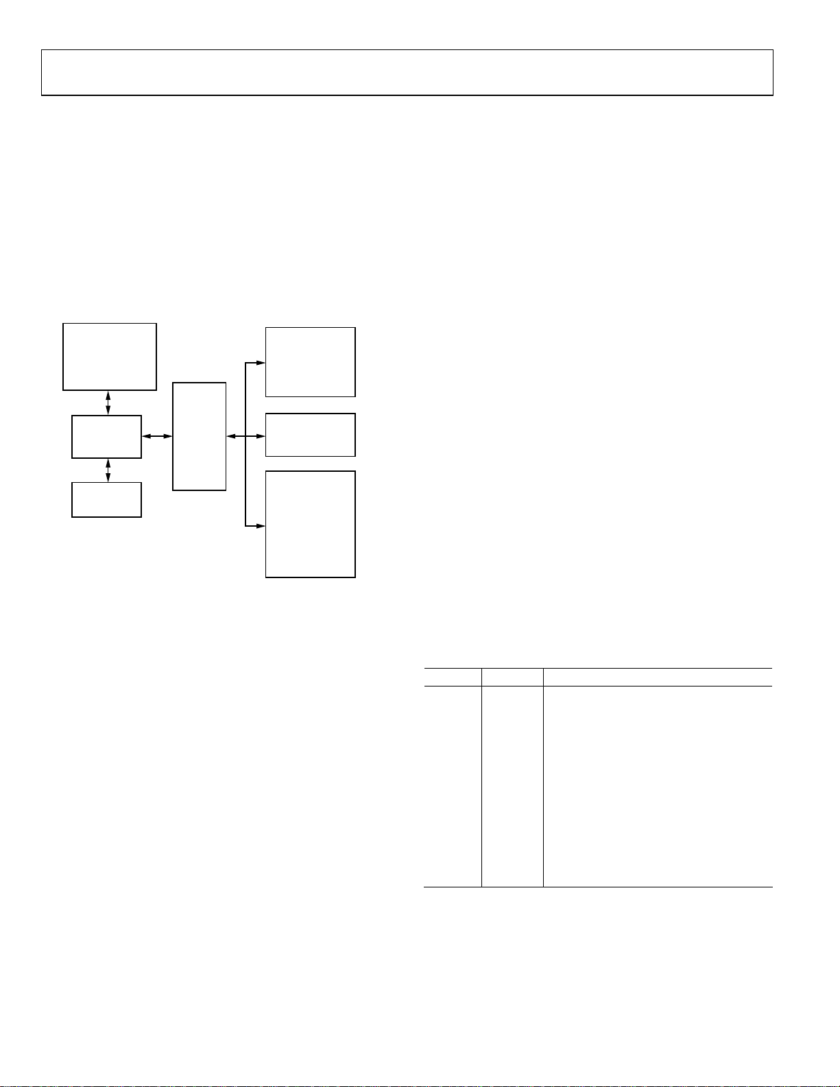
ADuC845/ADuC847/ADuC848
SPECIAL FUNCTION REGIST
The SFR space is mapped into the upper 128 bytes of internal
data memory space and accessed by direct addre
provides an inte face betwee
erals. A block diagra show
ADuC845/ADuC8 ADu
Figure 11.
All registers except the program counter (PC) and t
general- rpose re ster banks resi
isters in nt a registers that
reg clude co rol, configuration, and dat
provide an interface b erals.
62-kBYTE
ELECTRICALLY
REPROGRAMMABLE
NONVOLATILE
FLASH/EE PROGRAM
MEMORY
COMPATIBLE
256 BYTES RAM
2kBYTES XRAM
Accumulator SFR (ACC)
ACC is the accumulator register, which is used for math operations including addition, subtraction, integer multiplication and
division, and Boolean bit manipulations. The mnemonics for
accumulator-specific instructions usually refer to the
accumulator as A.
B SFR (B)
The B register is used with the accumulator for multiplication
and division operations. For other instructions, it can be treated
as a general-purpose scratch pad register.
r n the CPU and all on-chip periph-
m ing the programming model of the
47/ C848 via the SFR area is shown in
pu gi de in the SFR area. The SFR
etween the CPU and all on-chip periph
128-BYTE
8051-
CORE
SPECIAL
FUNCTION
REGISTER
AREA
Figure 11. Programming Model
ERS (SFRs)
ELECTRICALLY
REPROGRAMMABLE
NONVOLATILE
FLASH/EE DATA
MEMORY
OTHER ON-CHIP
PERIPHERALS
TEMPERATURE
CURRENT SOU
12-BIT DAC
SERIAL I/O
ssing only. It
he four
4-kBYTE
Σ-∆ ADC
SENSOR
RCES
WDT
PSM
TIC
PWM
04741-011
Data Pointer (DPTR)
The data pointer is made up o
f three 8-bit registers: DPP (page
byte), DPH (high byte), and DPL (low byte). These provide
memory addresses for internal code and data memory access.
The DPTR can be manipulated as a 16-bit register (DPTR =
DPH, DPL), although INC DPTR instructions automatically
carry over to DPP, or as three independent 8-bit registers (D
PP,
DPH, DPL).
The ADuC845/ADu 847/ADu
pointers. See the D Data
C C848 support dual data
ual Pointers section.
Stack Pointer (SP and SPH)
The SP SFR is the stack pointer, which is used to hold an
internal M add called the top
is nted be data is stored during P
executions. Although
RAM, the SP register i his
causes the stack to beg
As mentioned earlier, t ded 11-bit stack
po e th a bits needed to make up the 11-bit s
po the SBs of the SPH byte located at B7H. T
en SPH e EXSP (CFG84x.7) bit must be set;
othe the SPH R can be neither written to nor read fr
Pr (PSW)
Th FR contai s several bits that reflect the current
status of the CPU as li
SFR Address:
Power-On Default:
Bit Addressable:
RA ress of the stack. The SP register
increme fore USH and CALL
the stack can reside anywhere in on-chip
s initialized to 07H after a reset. T
in at location 08H.
he parts offer an exten
inter. Th ree extr tack
inter are three L o
able the SFR, th
rwise, SF om.
ogram Status Word
e PSW S n
sted in Table 5.
D0H
00H
Yes
able 5. PSW SFR Bit Designations
T
Bit No. Name Description
7 CY Carry Flag.
6 AC Auxiliary Carry Flag.
5 F0 General-Purpose Flag.
4, 3 RS1, RS0 Register Bank Select Bits.
RS1 RS0 Selected Bank
0 0 0
0 1 1
1 0 2
1 1 3
2 OV Overflow Flag.
1 F1 General-Purpose Flag.
0 P Parity Bit.
Rev. B | Page 24 of 108

ADuC845/ADuC847/ADuC848
Power Control Register (PCON)
The PCON SFR contains bits for power-saving options and
general-purpose status flags as listed in Table 6.
SFR Address: 87H
Power-On Default: 00H
Bit Addressable: No
Table 6. PCON SFR Bit Designations
Bit No. Name Description
7 SMOD Double UART Baud Rate.
0 = Normal, 1 = Double Baud Rate.
6 SERIPD
5 INT0PD INT0 Power-Down Interrupt Enable.
4 ALEOFF If set to 1, the ALE output is disabled.
3 GF1 General-Purpose Flag Bit.
2 GF0 General-Purpose Flag Bit.
1 PD
0 ----- Not Implemented. Write Don’t Care.
Serial Power-Down Interrupt Enable. If this
bit is set, a serial interrupt from either SPI
2
C can terminate the power-down
or I
mode.
If this bit is set, either a level (
negative-going transition (
INT0 pin terminates power-down mode.
Power-Down Mode Enable. If se
part enters power-down mode.
IT0 = 0) or a
IT0 = 1) on th
t to 1, the
e
ADuC845/ADuC847/ADuC848 Configuration Register
(CFG845/CFG847/CFG848)
The CFG845/C
FG847/CFG848 SFR contains the bits necessary
to configure the internal XRAM and the extended SP. By default,
it configures the user into 8051 mode, that is, extended SP, and
the internal XRAM are disabled. When using in a program, use
the part name only, that is, CFG845, CFG847, or CFG8
48.
SFR Address: AFH
Power-On Default: 00H
Bit Addressable: No
Table 7. CFG845/CFG847/CFG848 SFR Bit Designations
Bit No. Name Description
7 EXSP Extended SP Enable.
If this bit is set to 1, the stack rolls over
from SPH/SP = 00FFH to 0100H.
If this bit is cleared to 0, SPH SFR is
disabled and the stack rolls over from
SP = FFH to SP = 00H.
6 ---- Not Implemented. Write Don’t Care.
5 ---- Not Implemented. Write Don’t Care.
4 ---- Not Implemented. Write Don’t Care.
3 ---- Not Implemented. Write Don’t Care.
2 ---- Not Implemented. Write Don’t Care.
1 ---- Not Implemented. Write Don’t Care.
0 XRAMEN
If this bit is set to 1, the internal XRAM is
mapped into the lower 2 kbytes of the
external address space.
If this bit is cleared to 0, the internal XR
is accessible and up to 16 MB of external
data memory become available. See
Figure 8.
AM
Rev. B | Page 25 of 108

ADuC845/ADuC847/ADuC848
ADC CIRCUIT INFORMATION
The ADuC845 incorporates two 10-channel (8-channel on th
MQFP package) 24-bit Σ-∆ ADCs, while the ADuC847 and
ADuC848 each incorporate a single 10-channel (8-channel on
the MQFP package) 24-bit and 16-bit Σ-∆ ADC.
Each part also includes an on-chip programmable gain
amplifier and configurable buffering (neither is ava
ilable on the
auxiliary ADC on the ADuC845). The parts also incorporate
digital filtering intended for measuring wide dynamic range an
low frequency signals such as those in weigh-scale, strain-gage,
pressure transducer, or temperature measurement applicatio
The ADuC845/ADuC847/ADuC848 can be configured as four
or five (MQFP/LFCSP package) fully-differential input channel
or as eight or ten (MQFP/LFCSP package) pseudo differential
input channels referenced to AINCOM. The ADC on each part
(primary only on the ADuC845) can be fully buffered interna
and can be programmed for one of eight inp
±20 mV to ±2.56 V (V
× 1.024). Buffering the input channel
REF
ut ranges from
means that the part can handle significant source impedanc
on the selected analog input and that RC filtering (for noise
rejection or RFI reduction) can be placed on the analog inputs
If the ADC is used with internal buffering disabled
(ADC0CON1.7 = 1, ADC0CON1.6 = 0), these unbuffered
inputs provide a dynamic load to the driving source. Therefo
resistor/capacitor combinations on the inputs can cause dc gain
errors, depending on the output impedance of the source that is
driving the ADC in
puts.
Table 8 and Table 9 show the allowable external resistance/
capacitance values for unbuffered mode such that no gain error
at the 16-bit and 20-bit levels, respectiv
ely, is introduced. When
used with internal buffering enabled, it is recommended that a
e
ns.
lly,
es
re,
capacitor (10 nF to 100 nF) be placed on the input to the ADC
(usually as part of an antialiasing filter) to aid in noise
performance.
The input channels are intended to convert signals directly from
sensors without the need for external signal conditioning. With
internal buffering disabled (relevant bits set/cleared in
ADC0CON1), external buffering might be required.
d
When the internal buffer is enabled, it might be necessa
offset the negative input channel by +100 mV and to offset the
positive channel by −100 mV
if the reference range is AV
ry to
DD
.
This accounts for the restricted common-mode input range in
the buffer. Some circuits, for example, bridge circuits, are
tly suitable to use without having to offset where the
s
inheren
/2 and is not sufficiently
output voltage is balanced around
V
REF
large to encroach on the supply rails. Internal buffering is no
available
ADC (ADuC845 only) is fixed at a gain range of ±2
The ADCs use a Σ-Δ conversion technique to realize up t
on the auxiliary ADC (ADuC845 only). The auxiliary
.50 V.
o
t
24 bits on the ADuC845 and the ADuC847, and up to 16 bits on
.
the ADuC848 of no mis g codes performance (20 Hz update
rate, chop enabled). The Σ-Δ modulator converts the sampled
input signal into a digital pulse train whose duty cycle cont
the digital information. A sinc
(see Table 28) is then used to decimate the modulator output
data stream to give a valid da
able output rates. The signal chain has two modes of operation,
m
chop enabled and chop disabled. The
A
DCMODE register enables or disables the chopping scheme.
sin
3
programmable low-pass filter
ta conversion result at program-
bit in the
CHOP
ains
Table 8. Maximum Resistance for No 16-Bit Gain Error (Unbuffered Mode)
External Capacitance
Gain 0 pF 50 pF 100 pF 500 pF 1000 pF 5000 pF
1 111.3 kΩ 27.8 kΩ 16.7 kΩ 4.5 kΩ 2.58 kΩ 700 Ω
2 53.7 kΩ 13.5 kΩ 8.1 kΩ 2.2 kΩ 1.26 kΩ 360 Ω
4 25.4 kΩ 6.4 kΩ 3.9 kΩ 1.0 kΩ 600 Ω 170 Ω
8–128 10.7 kΩ 2.9 kΩ 1.7 kΩ 480 Ω 270 Ω 75 Ω
Table 9. Maximum Resistance for No 20-Bit Gain Error (Unbuffered Mode)
External Capacitance
Gain 0 pF 50 pF 100 pF 500 pF 1000 pF 5000 pF
1 84.9 kΩ 21.1 kΩ 12.5 kΩ 3.2 kΩ 1.77 kΩ 440 Ω
2 42.0 kΩ 10.4 kΩ 6.1 kΩ 1.6 kΩ 880 Ω 220 Ω
4 20.5 kΩ 5.0 kΩ 2.9 kΩ 790 Ω 430 Ω 110 Ω
8–128 8.8 kΩ 2.3 k Ω 1.3 k Ω 370 Ω 195 Ω 50 Ω
Rev. B | Page 26 of 108
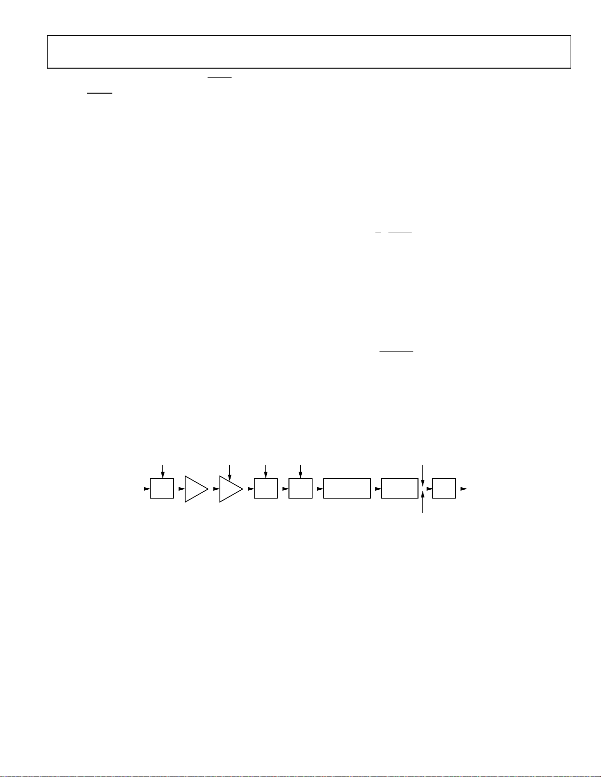
ADuC845/ADuC847/ADuC848
A
G
Signal Chain Overview (Chop Enabled,
With the
CHOP
bit = 0 (see the ADCMODE SFR bit designations in Table 24), the chopping scheme is enabled. This is the
default condition and gives optimum performance in terms of
offset errors and drift performance. With chop enabled, the
available output rates vary from 5.35 Hz to 105 Hz (SF = 255
and 13, respectively). A typical block diagram of the ADC input
channel with chop enabled is shown in Figure 12.
The sampling frequency of the modulator loop is many times
higher than the bandwidth of the input signal. The integrator in
the modulator shapes the quantization n
from the analog-to-digital conversion) so that the noise is pushe
toward one-half of the modulator frequency. The output of the
Σ-Δ modulator feeds directly into the digital filter. The digital
filter then band-limits the response to a frequency significantly
lower than one-half of the modulator frequency. In this manner,
the 1-bit output of the comparator is translated into a band
limited, low noise output from the ADCs.
3
The ADC filter is a low-pass Sinc
or (sinx/x)3 filter whose
primary function is to remove the quantization noise introduced
at the modulator. The cutoff frequency and decimated output
data rate of the filter are programmable via the Sinc filter word
loaded into the filter (SF) register (see Table 28). The complete
signal chain is chopped, resulting in excellent dc offset and
offset drift specifications and is extremely beneficial in applications where drift, noise rejection, and optimum EMI rejection
are important.
= 0)
CHOP
oise (which results
With
chop enabled, the ADC repeatedly reverses its inputs. The
deci
mated digital output words from the Sinc
have
a positive offset and a negative offset term included. As a
resu
lt, a final summing stage is included so that each output
word
from the filter is summed and averaged with the previous
filter
output to produce a new valid output result to be written
to th
e ADC data register. Programming the Sinc
3
filter, therefore,
3
decimation
factor is restricted to an 8-bit register called SF (see Table 28),
e actual decimation factor is the register value times 8.
th
Therefore, the decimated output rate from the Sinc
3
filter (and
the ADC conversion rate) is
d
1
f ×
SF
××=813
f
MODADC
where:
is the ADC conversion rate.
f
ADC
SF is the decimal equivalent of the word loaded to the filter
register.
is the modulator sampling rate of 32.768 kHz.
f
MOD
The chop rate of the channel is half the output data rate:
1
CHOP
As shown in the block diagram (Figure 12), the Sinc
outputs alternately contain +V
ff×=2
ADC
3
filter
and −VOS, where VOS is the
OS
respective channel offset.
NALO
INPUT
F
CHOP
MUX BUF
F
F
IN
MOD
Σ-∆
MOD
F
CHOP
XOR
SINC3 FILTERPGA 3 × (8 × SF)
t Channel with Chop Enabled Figure 12. Block Diagram of the ADC Inpu
F
ADC
AIN + V
AIN – V
Σ-∆
DIGITAL
2
OUTPUT
OS
OS
04741-013
Rev. B | Page 27 of 108
ADuC845/ADuC847/ADuC848
s offset i d by performing a r g avera 2.
Thi s remove unnin ge of
s average eans that the settling o any e in
Thi by 2 m time t chang
grammin e ADC is twice the no l conver time,
pro g of th rma sion
le an asy ous step change on th log inp ot
whi nchron e ana ut is n
reflecte he third subsequent t. See 13.
fully d until t outpu Figure
t ×== 2
SETTLE
f
2
ADC
t
ADC
SYNC
(I.E.
HRONOU NGE
S CHA
HANNEL GE)
CHAC N
e allowab nge for S op enab 13 to ith
Th le ra F (ch led) is 255 w
fault of espond nversi tes,
a de 69 (45H). The corr ing co on ra
nd pe eak no rforma are sho
rms a ak-to-p ise pe nces wn in
ble 10, Ta
Ta ble 11
cal and rated at a rential i oltage V
typi gene diffe nput v of 0
, Tabl e 1 nd Table he num are
2, a 13. T bers
and a common-mode voltage of 2.5 V. Note that the conversion time increases by 0.732 ms for each increment in
SF.
SAMPLE 1
NO/INVALID
SAMPLE 1
NO OUTPUT
SAMPLE 2 SAMPLE 3 SAMPLE 4 SAMPLE 5 SAMPLE 6
OUTPUT
SAMPLE 1 + SAMPLE 2
VALID OUTPUT
2
SAMPLE 2 + SAMPLE 3
VALID OU2TPUT
SAMPLE 3 + SAMPLE 4
2
NO OUTPUT
SAMPLE 4 + SAMPLE 5
VALID OUTP2UT
Figure 13. ADC Settling Time Following a Synchronous Change with
Chop Enabled
ASYNCH US CHA
RON
ISCONT US INPUT GE)
SAMPLE 2 SAMPLE 3 SAMPLE 4 SAMPLE 5 SAMPLE 6
SAMPLE 1 + SAMPLE 2
2
VALID OUTPUT
SAMPLE 2 + S
O NGE
INUO
SAMPLE 3 + SAMPLE 4
UNSETT2LED OUTPUT
AMPLE 3
2
CHAN(I.E. D
SAMPLE 4 + SAMPLE 5
2
SAMPLE 5 + SAMP
2
VALID OUTPUT
LE 6
04741-012
Figure 14. ADC Settlin
VALID OUTPUT
g Time Following an Asynchronous Change with
UNSETTLED OUTPUT
SAMPLE 5 + SAMPLE 6
VALID OUTPUT
2
04741-014
Chop Enabled
Rev. B | Page 28 of 108
ADuC845/ADuC847/ADuC848
ADC Noise Performance with Chop Enabled (
Table 10, Table 11, Table 12, and Table 13 show the output rm
noise and output peak-to-peak resolution in bits (rounded to
the nearest 0.5 LSB) for some typical output update rates for th
ADuC845, ADuC847, and ADuC848. The numbers are typica
and are generated at a differential input voltage of 0 V and a
common-mode voltage of 2.5 V. The output update rate is
selected via the SF7 to SF0 bits in the SF filter register. It is
important to note that the peak-to-peak resolution figures
represent the resolution for which there is no code flicker
within a 6-sigma limit.
The outp
the electrical noise in the semic uctor devices (device noise)
ut noise comes from two sources. The first source is
ond
Table 10. ADuC845 and ADuC847 Typical Output RMS Noise (µV) vs. Input Range and Update Rate with Chop Enabled
SF Word Data Update Rate (Hz) V ±640 mV ±1.28 V ±2.56 V ±20 mV ±40 mV ±80 mV ±160 mV ±320 m
13 105.03 1.75 1.30 1.65 1.5 2.1 3.1 7.15 13.3
23 59.36 1.25 0.95 1.08 0.94 1.0 1.87 3.24 7.1
27 50.56 1.0 1.0 0.85 0.85 1.13 1.56 2.9 3.6
69 19.79 0.63 0.68 0.52 0.7 0.61 1.1 1.3 2.75
255 5.35 0.31 0.38 0.34 0.32 0.4 0.45 0.68 1.22
Table 11. ADuC845 and ADuC847 Typical Peak-to-Peak Resolution (Bits) vs. Input Range and Update Rate with Chop Enabled
SF Word Data Update Rate (Hz) ±20 mV ±40 mV ±80 mV ±160 mV ±320 mV ±640 mV ±1.28 V ±2.56 V
13 105.03 12 13 14 15 15.5 16 16 16
23 59.36 12 13.5 14.5 15.5 16.5 16.5 17 16.5
27 50.56 12.5 13.5 15 16 16.5 17 17 17.5
69 19.79 13 14 15.5 16 17.5 17.5 18 18
255 5.35 14.5 15 16 17 18 18.5 19 19.5
Table 12. ADuC848 Typical Output Noise (µV) vs. Input Range and Update Rate with Chop Enabled
SF Word Data Update Rate (Hz) ±20 mV ±40 mV ±80 mV ±160 mV ±320 mV ±640 mV ±1.28 V ±2.56 V
13 105.03 1.75 1.30 1.65 1.5 2.1 3.1 7.15 13.3
23 59.36 1.25 0.95 1.08 0.94 1.0 1.87 3.24 7.1
27 50.56 1.0 1.0 0.85 0.85 1.13 1.56 2.9 3.6
69 19.79 0.63 0.68 0.52 0.7 0.61 1.1 1.3 2.75
255 5.35 0.31 0.38 0.34 0.32 0.4 0.45 0.68 1.22
Table 13. ADuC848 Typical Peak-to-Peak Resolution (Bits) vs. Input Range and Update Rate with Chop Enabled
SF Word Data Update Rate (Hz) ±20 mV ±40 mV ±80 mV ±160 mV ±320 mV ±640 mV ±1.28 V ±2.56 V
13 105.03 12 13 14 15 15.5 16 16 16
23 59.36 12 13.5 14.5 15.5 16 16 17 16
27 50.56 12.5 13.5 15 16 16 16 16 16
69 19.79 13 14 15.5 16 16 16 16 16
255 5.35 14.5 15 16 16 16 16 16 16
CHOP
= 0)
used in the implementation of the modulator. The second
s
source is quantization noise, which is added when the analog
input is converted to the digital domain. The device noise is at a
e
l
low level and is independent of frequency. The quantization
noise starts at an even lower level but rises rapidly with increasing
frequency to become the dominant noise source.
The numbers in the tables are given for the bipolar input ran
For the unipolar ran
ges, the rms noise numbers are in the same
ges.
range as the bipolar figures, but the peak-to-peak resolution is
based on half the signal range, which effectively means losing
1 bit of resolution.
Input Range
Input Range
Input Range
Input Range
Rev. B | Page 29 of 108

ADuC845/ADuC847/ADuC848
Signal Chain Overview with Chop Disabled (
With
= 1, chop is disabled and the available output rates
CHOP
vary from 16.06 Hz to 1.365 kHz. The range of applicable SF
words is from 3 to 255. When switching between channels with
chop disabled, the channel throughput rate is higher than wh
chop is enabled. The drawback with chop disabled is that the
drift performance is degraded and offset calibration is require
following a gain range change or significant temperature
change. A block diagram of the ADC input channel with chop
disable
d is shown in Figure 15.
The signal chain includes a multiplex or buffer, PGA, Σ-Δ
modulator, and digital filter. The modulator bit stream is
3
applied to a Sinc
ctor is restricted to an 8-bit register SF; the actual decimation
fa
filter. Programming the Sinc3 decimation
factor is the register value times 8. The decimated output rate
3
from the Sinc
f =
e:
wher
is the AD version rate.
f
ADC
the deci uivalent of th loade e filter
SF is
ter, valid ran rom 3 to 255.
regis
is the modulator sampling rate of 32.768 kHz.
f
D
MO
filter (and the ADC conversion rate) is therefore
1
SF×8
f×
MODADC
C con
mal eq
e word d to th
ge is f
CHOP
= 1)
en
d
The settling time to a step input is governed by the digital filte
A synchronized step change requires a settling time of three
r.
times the programmed update rate; a channel change can be
treated as a synchronized step change. This is one conversion
longer than the case for chop enabled. However, be
cause the
ADC throughput is three times faster with chop disabled than it
is with chop enabled, the actual time to a settled ADC output is
significantly less also. This means that following a synchronized
step change, the ADC requires three conversions (note: data is
not output following a synchronized ADC change until data h
as
settled) before the result accurately reflects the new input
voltage.
t ×== 3
SETTLE
f
3
ADC
t
ADC
An unsynchronized step change requires four conversions to
accur e new analog input at its output. Note that
ately reflect th
with an u ynchronize hange the C contin to outpu
data a the user t take un d output o accoun
Aga n with enable
bec ADC put w disa aster
with nable tual ti n to o sett
AD t is le
ns d c AD ues t
nd so mus settle s int t.
in, this is one conversion longer tha chop d, but
ause the through ith chop bled is f than
chop e d, the ac me take btain a led
C outpu ss.
The allowable range for SF is 3 to 255 with a default of 69 (45H).
The corresponding conversion rates, rms, and peak-to-peak
noise are shown in Table 14, Table 15, Table 16,
performances
and Tabl
for each
e 1 th n ti ases ms
7. Note that
incr SF.
ent in
em
e conversio me incre by 0.244
ANALOG
INPUT
F
IN
MUX BUF
Figure 15. Block Diagram of ADC Input Channel with Chop Disabled
F
MOD
Σ-∆
MOD
SINC3 FILTERPGA 8 × SF
F
ADC
DIGITAL
OUTPUT
04741-015
Rev. B | Page 30 of 108

ADuC845/ADuC847/ADuC848
ADC Noise Performance with Chop Disabl = 1)
Table 14, Table 15, Table 16, and Table 17 show the output rm
noise and output peak-to-peak reso
the neares LSB) for some typical out date
num pical and erentia
volt 2.5 V.
upda elected the S
regi at the p figure
the r r whi within
mit.
li
t 0.5 put up rates. The
bers are ty are generated at a diff l input
age of 0 V and a common-mode voltage of The output
te rate is s via the SF7 to SF0 bits in F filter
ster. Note th eak-to-peak resolution s represent
esolution fo ch there is no code flicker a 6-sigma
lution in bits (rounded to
The output noise comes from two sources. The first source is
the electrical noise in the semicond
used in th lementation of the modu The s
Tab C845 a utp
SF Word
3 1365.33 30.64 56.18 124.5 00.47 248.39 468.65 774.36 1739.5
13 315.08 2.07 1.95 2.28 3.24 8.22 13.9 20.98 49.26
68 59.36 0.85 0.79 1.01 0.99 0.79 1.29 2.3 3.7
82 49.95 0.83 0.77 0.85 0.77 0.91 1.12 1.59 3.2
255 16.06 0.52 0.58 0.59 0.48 0.52 0.57 1.16 1.68
e imp lator. econd
le 14. ADu nd ADuC847 Typical O ut RMS Noise (µV) vs
Da ate
ta Upd
Ra )
te (Hz
uctor devices (device noise)
±20 mV V ±80 mV ± 0 mV ±1.28 V ±2.56 V
ble 15. AD nd ADuC847 Typical P ak Resolution (B
Ta uC845 a eak-to-Pe its) vs. Input Range and Update Rate with Chop Disabled
pdate
Data U
SF Word
3 1365.33 7.5 9 99 9 9 9 9
13 315.08 11.5 13.5 112.5 4 13.5 14 14 14
68 59.36 13 14 14.5 15.5 17 17 17.5 18
82 49.95 13 14 15 16 16.5 17.5 18 18
255 16.06 13.5 14.5 15.5 16.5 17.5 18.5 18.5 19
Rate (Hz)
±20 mV V ±80 mV ±
Table 16. uC848 Typical Output R ise (µV) nd Update Rate with Chop Disabled
SF Word
3 1365.33 30.64 56.18 124.5 00.47 248.39 468.65 774.36 1739.5
13 315.08 2.07 2.28 3.24 8.22 13.9 20.98 49.26 1.95
69 59.36 0.85 1.01 0.99 0.79 1.29 2.3 3.7 0.79
82 49.95 0.83 0.77 0.85 0.77 0.91 1.12 1.59 3.2
255 16.06 0.52 0.58 0.59 0.48 0.52 0.57 1.16 1.68
AD MS No vs. Input Range a
Hz)
date
±20 mV mV ±80 mV ±
Data Up
Rate (
Table 17. ADuC848 Typical Peak-to-Peak Resolution (Bits ange and Update Rate with Chop Disabled
Data Update
SF Word
3 1365.33 7.5 9 9 9 9 9 9 9
13 315.08 11.5 12.5 13.5 14 13.5 14 14 14
68 59.36 13 14 14.5 15.5 16 16 16 16
82 49.95 13 14 15 16 16 16 16 16
255 16.06 13.5 14.5 15.5 16 16 16 16 16
Rate (Hz)
±20 mV ±40 mV ±80 mV ±160 mV ±320mV ±640mV ±1.28 V ±2.56 V
ed (
CHOP
s
source is quantization noise, which is added when the analog
input is converted to the digital domain. The device noise is at a
low level and is independent of frequency. The quantization
noise starts at an even lower level but rises rapidly with increasi
frequency to become the dominant noise source.
The numbers in the tables are given for the bipolar input ranges.
For the unipolar ranges, the rms noise numbers are the same as
the bipolar range, but the peak-to
-peak resolution is based on
half the signal range, which effectively means losing 1 bit of
resolution. Typically, the performance of the ADC with chop
disabled shows a 0.5 LSB degradation over the performance
with chop enabled.
. Input Range and Update Rate with Chop Disabled
Input Range
±40 m 160 mV ±320 mV ±64
Input Range
±40 m 160 mV ±320 mV ±640 mV ±1.28 V ±2.56 V
Input Range
±40 160 mV ±320 mV ±640 mV ±1.28 V ±2.56 V
) vs. Input R
Input Range
ng
Rev. B | Page 31 of 108

ADuC845/ADuC847/ADuC848
AUXILIARY ADC (ADUC845 ONLY)
Table 18. ADuC845 Typical Output RMS Noise (µV) vs.
Update Rate with Chop Enabled
SF Word Data Update Rate (Hz) µV
13 105.03 17.46
23 59.36 3.13
27 50.56 4.56
69 19.79 2.66
255 5.35 1.13
Table 19. ADuC845 Typical Peak-to-Peak Resolution (Bits)
Update Rate
SF Word Data Update Rate (Hz) Bits
13 105.03 15.5
23 59.36 18
27 50.56 17.5
69 19.79 18
255 5.35 19.5
1
ADC converting in bipolar mode.
1
with Chop Enabled
Table 20. ADuC845 Typical Output RMS Noise (µV) vs.
Update Rate with Chop Disabled
SF Word Data Update Rate (Hz) µV
3 1365.33 1386.58
13 315.08 34.94
66 62.06 3.2
69 59.36 3.19
81 50.57 3.14
255 16.06 1.71
Table 21. ADuC845 Peak-to-Peak Resolution (Bits) vs.
Update Rate with Chop Disabled
SF Word Data Update Rate (Hz) Bits
3 1365.33 9
13 315.08 14.5
66 62.06 18
69 59.36 18
81 50.57 18
255 16.06 19
REFERENCE INPUTS
The ADuC845/ADuC847/ADuC848 each have two separate
differential reference inputs, REFIN± and REFIN2±. While
both references are available for use with the primary ADC,
only REFIN± is available for the auxiliary ADC (ADuC845
only). The common-mode range for these differential
references is from AGND to AV
reference voltage is 2.5 V, with the primary and auxiliary
(ADuC845 only)
reference select bits configured from the
ADC0CON2 and ADC1CON (ADuC845 only), respectively.
. The nominal external
DD
vs.
When an external reference voltage is used, the primary ADC
sees this internally as a 2.56 V reference (V
Therefore, any calculat
For instance, with a 2.5
ions of LSB size should account for this.
V external reference connected and
using a gain of 1 on a unipolar range (2.56 V), the LSB size i
24
(2.56/2
) = 152.6 nV (if using the 24-bit ADC on the ADuC8
or ADuC847). If a bipolar gain of 4 is used (±640 mV), th
24
size is (±640 mV)/2
on the ADuC845 or ADuC84
) = 76.3 nV (again using the 24-bit ADC
7).
× 1.024).
REF
s
45
e LSB
The ADuC845/ADuC847/ADuC848 can also be configured to
use the on-chip band gap reference via the XREF0/1 bits in the
ADC0CON2 SFR (for primary ADC) or the AXREF bit in
ADC1CON (for auxiliary ADC (ADuC845 only)). In this mode
of operation, the ADC sees the internal reference of 1.25 V,
thereby halving all the input ranges. A consequence of using th
internal ba in peak-
nd gap reference is a noticeable degradation
to-peak resolution. For this reason, operation with an external
reference is recommended.
In applications where the excitation (voltage or current) for the
transducer on the analog input also drives the reference inputs
for the part, the effect of any low frequency noise in the
excitation source is removed because the application is ratiometric. If the parts are not used in a ratiometric configuratio
n, a
low noise reference should be used. Recommended reference
voltage sources for the ADuC845/ADuC847/ADuC848 include
ADR421, REF43, and REF192.
The reference inputs provide a high impedance, dynamic
to external connections. Because the impedance of each refer
load
ence
input is dynamic, resistor/capacitor combinations on these pins
can cause dc gain errors, dep
the source that is driv
sources, such as those me
ending on the output impedance of
ing the reference inputs. Reference voltage
ntioned above, for example, the
ADR421, typically have low output impedances, and, therefore,
decoupling capacitors on the REFIN± or REFIN2± inputs w
ould
be recommended (typically 0.1 µF). Deriving the reference
voltage from an external resistor configuration means that the
reference input sees a significant external source impedance.
External decoupling of the REFIN± and/or REFIN2± inputs is
not recommended in this type of configuration.
BURNOUT CURRENT SOURCES
The primary ADC on the ADuC845 and the ADC on the
ADuC847 and ADuC848 incorporate two 200 µA constant
current genera
connected sensor. One sources current from the AV
AIN(+), and one sinks current from AIN(−) to AGND. These
currents are only configurable for use on AIN5/AIN6 and/or
AIN7/AIN8 in differential mode only, from the ICON.6 bit in
the ICON SFR (see Table 30). These burnout current sources
are also available only with buffering enabled via the BUF0/BUF1
bits in the ADC0CON1 SFR. Once the burnout currents are
turned on, a current flows in the external transducer circuit,
tors that are used to detect a failure in a
DD
to
e
Rev. B | Page 32 of 108

ADuC845/ADuC847/ADuC848
A
G
and a measurement of the input voltage on the analog input
channel can be taken. When the resulting voltage meas
full scale, the transduce
measured is 0 V, this i
r has gone open circuit. When the voltage
ndicates that the transducer has gone
ured is
short circuit. The current sources work over the normal
absolute input voltage range specifications.
REFERENCE DETECT CIRCUIT
The main and auxiliary (ADuC845 only) ADCs can be configured to allow the use of the internal band gap reference or an
external reference that is applied to the REFIN± pins by means
of the XREF0/1 bit in the Control Registers AD0CON2 and
AD1CON (ADuC845 only). A reference detection circuit is
provided to detect whether a valid voltage is applied to the
REFIN± pins. This feature arose in connection with strain-gage
sensors in weigh scales where the reference and signal are
provided via a cable from the remote sensor. It is desirable to
detect whether the cable is disconnected. If either of the pins is
floating or if the applied vol
flag (NOXREF) is set in t
conversion results a
updated if a calibration is in progress.
Note that the reference detect does not look at REFIN2± pins.
If, during either an offset or gain calibration, the NOEXRE
becomes active, indicating an incorrect V
relevant calibration register is inhibited to avoid loading
incorrect data into these registers, and the appropriate bits in
ADCSTAT (ERR0 or ERR1) are set. If the user needs to verify
that a valid reference is in place every time a calibration is
performed, the status of the ERR0 and ERR1 bits should be
checked at the end of every calibration cycle.
tage is below a specified threshold, a
he ADC status register (ADCSTAT),
re clamped, and calibration registers are not
F bit
, updating the
REF
clock (modulator rate) of 32.768 kHz. During calibration, the
current (user-written) value of the SF register is used.
Σ- MODULATOR
A Σ-∆ ADC usually consists of two main blocks, an ana
modulator, and a digital filter. For the ADuC845/ADuC847/
ADuC848, the analog modulator consists of a difference
amplifier, an integrator block, a comparator, and a feedback
DAC as shown in Figure 16.
NALO
INPUT
DIFFERENCE
AMP
INTEGRATOR
DAC
Figure 16. Σ-∆ Modulator Simplified Block Diagram
COMPARATOR
In operation, the analog signal is fed to the difference amplifier
along with the output from the feedback DAC. The difference
between these two signals is integrated and fed to the comparator.
The output from the comparator provides the input to the feedback DAC so the system f unctions as a negative feedback loop
that tries to minimize the difference signal. The digital data th
represents the analog input voltage is contained in the duty
cycle of the pulse train appearing at the output of the comparato
This duty cycle data can be recovered as a data-wor
subsequent digital filter stage. The sampling frequency of the
modulator loop is many times higher than the bandwidth o
input signal. The integrator in the modulator shapes the
quantization noise (that results from the analog-to-digital
conversion) so that the noise is pushed toward one-half of t
modulator frequency.
log
HIGH
FREQUEN
BIT STREAM
TO DIGITAL
FILTER
CY
04741-016
d by using a
f the
he
at
r.
SINC FILTER REGISTER (SF)
The number entered into the SF register sets the decimation
factor of the Sinc
The range of operation of the SF w
ADC chop is on or off. With chop disabled, the minimum SF
word is 3 and the maximum is 255. This gives an ADC throughput rate from 16.06 Hz to 1.365 kHz. With chop enabled, the
minimum SF word is 13 (all values lower than 13 are clamped
to 13) and the maximum is 255. This gives an ADC throug
rate of 5.4 Hz to 105 Hz. See the f
description preceding section.
An additional feature
positioned in the frequency response at 60 Hz. This gives
simultaneous 60 Hz rejection to whatever notch is defined by
the SF filter. This 60 Hz filter is enabled via the REJ60 bit in th
ADCMOD
for SF words ≥ 68; otherwise, ADC errors occur, and, the no
is best used with an SF word of 82d giving simultaneous 50 Hz
and 60 Hz rejection. This function is useful only with an ADC
3
filter for the ADC. See Table 28 and Table 29.
ord depends on whether
hput
equation in the ADC
ADC
3
of the Sinc
filter is a second notch filter
E register (ADCMODE.6). The notch is valid only
Rev. B | Page 33 of 108
tch
DIGITAL FILTER
The output of the ∑-∆ modulator feeds directly into the digital
filter. The digital filter then band-limits the response to a
frequency significantly lower than one-half of the modulator
frequency. In this manner, the 1-bit output of the comparator is
translated into a ba
The ADuC845/ADuC847/ADuC
or [(SINx)/x]
quantization noise introduced at the modulator. The cutoff
frequency and decimated output data rate of the filter are
programmable via the SF (Sinc filter) SFR as listed in Table 28
and Table 29.
Figure 22, Figure 23, Figure 24, and Figure 25 show the frequency
response of the ADC, yielding an overall output rate of 16.6 H
e
with chop enabled and 50 Hz with chop disabled. Also detailed
in these plots is the effect of the fixed 60 Hz drop-in notch filter
(REJ60 bit, ADCMODE.6). This fixed filter can be enabled or
disabled by setting or clearing the REJ60 bit in the ADCMO
register (ADCMODE.6). This 60 Hz drop-in notch filter can be
nd-limited, low noise output from the part.
848 filter is a low-pass, Sinc
3
filter whose primary function is to remove the
3
DE
z

ADuC845/ADuC847/ADuC848
enabled for any SF word that yields an ADC throughput that i
less than 20 Hz with chop enabled (SF ≥ 68 decimal).
ADC CHOPPING
The ADCs on the ADuC845/ADuC847/ADuC848 implement a
chopping scheme whereby the ADC repeatedly reverses its
inputs. The decim
therefore, have a positive and negative offset term in
a result, a final summing stage is included in each A
each output word from the filter is summed and averaged with
the previous filter output to produce a new valid output result
to be written to the ADC data SFRs. The ADC throughput or
update rate is listed in Table 29. The chopping scheme
porated into the parts results in
drift specifications, and is extremely beneficial in applications
where drift, noise rejection, and optimum EMI performan
important. ADC chop can be disabled via the chop bit in the
ADCMODE SFR (ADCM
hig ) disables chop mode.
h
CAL
IBRATION
The /ADuC847/ADuC848 incorporate four calibration
ADuC845
mod
es that can be programmed via the mode bits in the
ADC
MODE SFR detailed in Table 24. Every part is calibrated
befo
re it leaves the factory. The resulting offset and gain
b
cali ration coefficients for both the primary and auxiliary
(AD uring-
uC845 only) ADCs are stored on-chip in manufact
speci
fic Flash/EE memory locations. At power-on or after a
rese
t, these factory calibration registers are automatically
dow SFR
nloaded to the ADC calibration registers in the part’s
space. To facilitate user calibration, each of the primary and
auxiliary (ADuC845 only) ADCs have dedicated calibration
control SFRs, which are described in the ADC SFR Interface
section. Once a user initiates a calibration procedure, the factory
calibration values that were initially downloaded during the
power-on sequence to the ADC calibration S
The ADC to be calibrated must be enabled via
bits in the ADCMODE register.
Even though an internal offset calibration mode is described in
this section, note that the ADCs can be chopped. This chopping
scheme inherently minimizes offset errors and means that an
offset calibration should never be required. Also, because
factory 5 V/25°C gain calibration coefficients are automatically
present at power-on, an internal full-scale calibration is requ
only if the part is operated at 3 V or at temperatures significantly
different from 25°C.
If the part is operated in chop disabled mode, a calibration
need to be done with every gain range change that occurs vi
the PGA.
The ADuC845/ADuC847/ADuC848 each offer internal or
system calibration facilities. For full calibration to occur on the
selected ADC, the calibration logic must record the modulator
ated digital output words from the Sinc
DC so that
excellent dc offset and offset
ODE.3). Setting this bit to 1 (logic
FRs are overwritten.
the ADC enable
s
3
filter,
cluded. As
incor-
ce are
ired
may
a
output for two input conditions: zero-scale and full-scale points
These points are derived by performing a conversion on the
different input voltages (zero-scale and full-scale) provided to the
input of the modulator during calibration. The result of the
zero-scale calib
calibration registers for the appropriate ADC. The r
full-scale calibration conversion is stored in the gain calibratio
registers for the appropriate ADC. With these readings, the
calibration logic can calculate the offset and the gain slope fo
the input-to-output transfer function of the converter.
During an internal zero-scale or full-scale calibration, the
respective zero-scale input or full-scale input is automatically
connected to the ADC inputs internally. A system calibration,
however, expects the system
voltages to be applied externally to the ADC pins by the user
before the calibration mode is initiated. In this way, external
errors are taken into account and minimized. Note that all
ADuC845/ADuC847/ADuC848 ADC calibrations are carried
out at the user-selected SF word update rate. To optimize
calibration accuracy, it is recommended that the slowest possible
update rate be used.
Internally in the
being used to scale the words coming out of the digital filter.
The offset calibration coefficient is subtracted from the result
prior to the multiplication by the gain coefficient.
From an operational point of view, a calibration should be
treated just like an ordinary ADC conversion. A zero-scale
calibration (if required) should always be carried out before a
full-scale calibration. System software should monitor the
relevant ADC RDY0/1 bit in the ADCSTAT SFR to determine
the end of calibration by using a polling sequence or an interrup
driven routine. If required, the NOEXREF0/1 bits can be moni
tored to detect unconnected or low voltage errors in the referenc
during conversion. In the event of the reference becoming
disconnect
calibration is immediately halted and no write to the calibration
SFRs takes pla
Internal Calibration Example
With chop e should
never be required, although a full-scale or gain calibration may
be required. However, if a full internal calibration is required,
the procedure should be to select a PGA gain of 1 (±2.56 V) and
perform a zero-scale calibration (MD2...0 = 100B in the
ADCMODE register). Next, select and perform full-scale
calibration by setting MD2...0 = 101B in the ADCMODE SFR.
Now select the desired PGA range and perform a zero-scale
calibration again (MD2..0 = 100B in ADCMODE) at the new
PGA range. The reason for the double zero-scale calibration is
that the internal calibration procedure for full-scale calibration
automatically selects the reference in voltage at PGA = 1.
ration conversion is stored in the offset
esult of the
zero-scale and system full-scale
parts, the coefficients are normalized before
ed, causing a NOXREF flag during a calibration, the
ce.
nabled, a zero-scale or offset calibration
.
n
r
t
e
Rev. B | Page 34 of 108

ADuC845/ADuC847/ADuC848
Therefore, the full-scale endpo
subtracts the offset calibration error, it is advisable to perform
an offset calibration at the same gain range as that used for fullscale calibration. There is no penalty to the full-scale calibration
in redoing the zero-scale calibration at the required PGA range
because the full-scale calibration has very good matching at all
the PGA ranges.
This p a ed.
rocedure also applies when chop is dis bl
at for internal calibration to be effective, the AIN− pin
Note th
should b
e held at a steady voltage, within the allowable common-
mode range to keep it from floatin
System Calibration Example
With chop enabled, a system zero-scale or offset calibration
should never be required. However, if a full-scale or gain
calibration is required for any reason, use the following typica
procedure for doing so.
1. i e of 0 V to the selected analog
Apply a different al voltag
inputs (AIN+ to AIN−) that are held at a common-mode
voltage.
Perform a system zero-scale or offset calibration by setting
the MD2...0 bits in the ADCMODE register to 110B.
2. Apply a full-scale differential voltage across the ADC
inputs again at the same common-mode voltage.
Perform a system full-scale or gain cal ration b
the MD2 its in the ADCMODE register to 1
Perform
...0 b 11B.
a system calibration at the required PGA range to be
used since the ADC scales to the
applied to the ADC during the calibration routines.
In bipolar mode, the zero-scale
scale point of the ADC (800000
PROGRAMMABLE GAIN AMPLIFIER
The primary ADC incorporates an on-chip programmable gain
amp rogrammed through eight
lifier (PGA). The PGA can be p
different ranges, which are prog mmed via the range bits (RN0
o RN2) in the ADC0CON1 register. With an external 2.5 V
t
ference applied, the unipolar ranges are 0 mV to 20 mV, 0 mV
re
to 40 mV, 0 mV to 80 mV, 0 mV to 160 mV, 0 mV to 320 mV,
0 mV to 640 mV, 0 V to 1.28 V and 0 V to 2.56 V, while in
bipolar mode the ranges are ±20 mV, ±40 mV, ±80 mV, ±160 mV,
±320 mV, ±64 0 mV, ±1.28 V, and ±2.56 V. These ranges should
appear on the input to the on-chip PGA. The ADC rangematching specification of 2 µV (typical with chop enabled)
means that calibration need only be carried out on a single
range and need not be repeated when the ADC range is
changed. This is a significant advantage compared to similar
int calibration automatically
g during calibration.
ib y setting
differential voltages that are
calibration determines the mid-
H) or 0 V.
ra
mixed-signal solutions availabl
(ADuC845 only) ADC does not incorporate a PGA, and the
gain is fixed at 0 V to 2.50 V in unipolar mode, and ±2.50 V
bipolar mode.
e on the market. The auxiliary
in
BIPOLAR/UNIPOLAR CONFIGURATION
The analog inputs of the ADuC845/ADuC847/ADuC848 can
accept either unipolar or bipolar input voltage ranges. Bipolar
input ranges do not imply that the part can handle negative
voltages with respect to system AGND, but rather with respec
to the negative reference input. Unipolar and bipolar signals on
the AIN(+) input on the ADC are referenced to the voltage on
the respective AIN(−) input. AIN(+) and AIN(−) refer to the
signals seen by the ADC.
For example, if AIN(−) is biased to 2.5 V (tied to the external
l
reference voltage) and the ADC is configured for a unipolar
analog input range of 0 mV to >20 mV, the input volta
on AIN(+) is 2.5 V to 2.52 V. O he other hand, if AIN(−) is
n t
biased to 2.5 V (again the external reference voltage) and the
ADC is configured for a bipolar analog input range of ±1.28 V,
the analog input range on the AIN(+) is 1.22 V to 3.78 V, that is,
2.5 V ± 1.28 V.
The modes of operation for the ADC are fully differential mode
or pseudo differential mode. In fully differential mode, AIN1 to
AIN2 are one differential pair, and AIN3 to AIN4 are another
pair (AIN5 to AIN6, AIN7 to AIN8, and AIN9 to AIN10 are the
others). In differential mode, all AIN(−) pin names imply the
negative analog input of the selected differential pair, that is,
AIN2, AIN4, AIN6, AIN8, AIN10. The term AIN(+) implies
the positive input of the selected differential pair, that is, AIN1,
AIN3, AIN5, AIN7, AIN9. In pseudo differential mode, each
analog input is paired with the AINCOM pin, which can be
biased up or tied to AGND. In this mode, the AIN(−) implies
AINCOM, and AIN(+) implies any one of the ten analog input
channels.
The configuration of the inputs (unipolar vs. bipolar) is shown
in Figure 17.
AIN1
AIN2
INPUT 1
INPUT 2
INPUT 3
INPUT 4
INPUT 5
INPUT 6
INPUT 7
Figure 17. Unipolar and Bipolar Channel Pairs
AIN3
AIN4
AIN5
AIN6
AIN7
AIN8
AIN9
INPUT 8
AIN10
INPUT 9
INPUT 10
AINCOM
FULLY DIFFERENTIAL
FULLY DIFFERENTIAL
FULLY DIFFERENTIAL
FULLY DIFFERENTIAL
CSP PACKAGE
FULLY DIFFERENTIAL
ADuC845/ADuC847/ADuC848
AIN1
AIN2
AIN3
AIN4
AIN5
AIN6
AIN7
AIN8
AIN9
AIN10
AINCOM
t
ge range
CSP PACKAGE
ADuC845/ADuC847/ADuC848
04741-017
Rev. B | Page 35 of 108

ADuC845/ADuC847/ADuC848
DATA OUTPUT CODING
When the primary ADC is configured for unipolar operation,
the output coding is natural (straight) binary with a zero differential input voltage resulting in a code of 000...000, a midscale
voltage resulting in a code of 100...000, and a full-scale voltage
resulting in a code of 111...111. The output code for any analog
input voltage on the main ADC can be represented as follows:
N
Code – (AIN × GAIN × 2
)/(1.024 × V
where:
AIN is the analog input voltage.
GAIN is the PGA gain setting, that is, 1 on the 2.56 V range and
128 on the 20 mV range, and N = 24 (16 on the ADuC848).
The output code for any analog input voltage on the auxiliary
ADC can
be represented as follows:
N
Code = (AIN × 2
)/(V
REF
)
with the same definitions as used for the primary ADC above.
REF
)
EXCITATION CURRENTS
The ADuC845/ADuC847/ADuC848 contain two matched,
software-configurable 200 µA current sources. Both source
current from AV
, which is directed to either or both of the
DD
IEXC1 (Pin 11 whose alternate functions are P1.6/AIN7) or
IEXC2 (Pin 12, whose alternate functions are P1.7/AIN8) pins
on the device. These currents are controlled via the lower four
bits in the ICON register (Table 30). These bits not only enable
the current sources but also allow the configuration of the
currents such that 200 µA can be sourced individually from
both pins or can be combined to give a 400 µA source from one
or the other of the outputs. These sources can be used to excite
external resistive bridge or RTD sensors (see Figure 71).
ADC POWER-ON
The ADC typically takes 0.5 ms to power up from an initial
start-up seque
nce or following a power-down event.
When the primary ADC is conf ured for bipolar operation, the
ig
coding is offset binary with negative full-scale voltage resulting
in a code of 000...000, a zero differential voltage resulting in a
code of 800…000, and a positive full-scale voltage resulting in a
code of 111...111. The output from the primary ADC for any
analog input voltage can be represented as follows:
Code = 2
[(AIN × GAIN)/(1.024 ×V
REF
) + 1]
N−1
where:
AIN is the analog input voltage.
GAIN is the PGA gain, that is, 1 on the ±2.56 V range and
128 on the ±20 mV range.
N = 24 (16 on the ADuC848).
The output from the auxiliary ADC in bipolar mode can be
represented as follows:
Code = 2
[(AIN/V
REF
) + 1]
N−1
Rev. B | Page 36 of 108

ADuC845/ADuC847/ADuC848
RACTERISTICS TYPICAL PERFORMANCE CHA
0
–10
–20
–30
–40
–5
0
dB)
–60
GAIN (
–70
–80
–90
–100
–110
–120
010
20304050 9080 1007060 110
FREQUENCY (Hz)
Figure 18. Filter Response, Chop On, SF = 69 Decimal
–10
–30
–50
–70
–90
AMPLITUDE (dB)
–110
–130
–150
01020304050 9080 1007060
FREQUENCY (Hz)
Figure 19. Filter Response, Chop On, SF = 255 Decimal
0
–10
–20
–30
–40
–50
–60
GAIN (dB)
–70
–80
–90
–100
–110
–120
10 30 50 70 90 110 210190170 230150130 250
SF (Decimal)
Figure 20. 50 Hz Normal Mode Rejection vs. SF Word, Chop On
04741-018
04741-019
04741-020
0
–10
–20
–30
–40
–50
B)
–60
GAIN (d
–70
–80
–90
–100
–110
–120
10 30 50 70 90 110 150130
SF (Decimal)
Figure 21. 60 Hz Normal Mode Rejection vs. SF, Chop On
10
–10
–30
–50
–70
–90
AMPLITUDE (dB)
–110
–130
–150
0.1
10.1
20.1
30.1
40.1
50.1
60.1
90.1
80.1
70.1
FREQUENCY (Hz)
100.1
110.1
120.1
Figure 22. Chop Off, Fadc = 50 Hz, SF = 52H
10
–10
–30
–50
–70
–190
AMPLITUDE (dB)
–110
–130
–150
0.1
10.1
20.1
30.1
40.1
50.1
60.1
90.1
80.1
70.1
FREQUENCY (Hz)
100.1
110.1
120.1
Figure 23. Chop Off, SF = 52H, REJ60 Enabled
210190170 230 250
150.1
140.1
130.1
150.1
140.1
130.1
160.1
160.1
170.1
170.1
04741-021
04741-022
04741-023
Rev. B | Page 37 of 108

ADuC845/ADuC847/ADuC848
LITUDE (dB)
AMP
–100
–120
0
–20
–40
–60
–80
5
0
25
201015
30
35
FREQUENCY (Hz)
55
504045
Figure 24. Chop On, Fadc = 16.6 Hz, SF = 52H
60
100
04741-024
95
90
85
757080
65
0
–20
–40
–60
AMPLITUDE (dB)
–80
–100
–120
5
0
25
201015
35
30
FREQUENCY (Hz)
55
504045
757080
65
60
Figure 25. Chop On, Fadc = 16.6 Hz, SF = 52H, REJ60 En
95
90
85
100
04741-025
abled
Rev. B | Page 38 of 108

ADuC845/ADuC847/ADuC848
FUNCTIONAL DESCRIPTION
ADC SFR INTERFACE
The ADCs are n led and
sections.
Table 22. ADC SF terfa
ame Description
N
ADCSTAT ADC Status Register. Holds the general status of the primary and auxiliary (ADuC845 only) ADCs.
ADCMODE ADC Mode Register. Controls the general modes of operation for primary and auxiliary (ADuC845 only) ADCs.
ADC0CON ary ADC Con onfiguration of the primary ADC. 1 Prim trol Register 1. Controls the specific c
ADC0CON y ADC Con nfiguration of the primary ADC. 2 Primar trol Register 2. Controls the specific co
ADC1CON iliary ADC ConAux trol Register. Controls the specific configuration of the auxiliary ADC. ADuC845 only.
SF
ICON t Source CoCurren ntrol Register. Allows user control of the various on-chip current source options.
ADC0L/M/H
ADC1L/M/H Auxiliary ADC 24-bit conversion result is held in these two 8-bit registers. ADuC845 only.
OF0L/M/H -b these three 8-bit registers. OF0L is not available on the ADuC848. Primary ADC 24 it offset calibration coefficient is held in
OF1L/H C 16-Auxiliary AD bit offset calibration coefficient is held in these two 8-bit registers. ADuC845 only.
GN0L/M/H Primary ADC 24-bit gain cali ADuC848. bration coefficient is held in these three 8-bit registers. GN0L is not available on the
GN1L/H xiliary ADC 16-Au bit gain calibration coefficient is held in these two 8-bit registers. ADuC845 only.
co trol configured via a number of SFRs that are mentioned here and described in more detail in the following
R In ce
3
Sinc Filter Registe
only) ADC update
Primary ADC 24-b lable on
the ADuC848.
r. Configures the decimation factor for the Sinc
rates.
it (16-bit on the ADuC848) conversion result is held in these three 8-bit registers. ADC0L is not avai
filter and, therefore, the primary and auxiliary (ADuC845
Rev. B | Page 39 of 108

ADuC845/ADuC847/ADuC848
ADCSTAT (ADC STATUS REGI
This SFR reflects the status of both ADCs including data ready, c
clu derflow fl s.
in ding REFIN± reference detect and conversion overflow/un
SFR
Address: D8H
Pow
er-On Default: 00H
Bit A
ddressable: Yes
Tabl
e 23 . ADC S TAT S F R Bit D e sig nati on
Bit N
o. Name Description
7
6 ADC.
5
4 primary o u
3
2 finition as ERR0 referred to the auxiliary ADC. Valid on the ADuC845 only. ERR1 Auxiliary ADC Error Bit. Same de
1 ––– Not Implemented. Write Don’t Care.
0 ––– Not Implemented. Write Don’t Care.
RDY0 Ready Bit for the Primary ADC.
Set by hardware on completion of conv
Cleared directly b
inhibited from writing further re
RDY1 Ready Bit for Auxiliary (ADuC845 only)
Same definition as RDY0 referred to the
CAL Calibration Status Bit.
Set by hardware on completion of cali
Cleared indirectly by a write to the
Note that calibration with the temperatur
NOXREF No External Reference Bit (only active if
Set to indicate that one or both of the REFIN pin
When set, conversion results are clam
Cleared to indicate valid V
ERR0 Primary ADC Error Bit.
Set by hardware to indicate that the
all 1s. After a calibration, this bit also flags er
Cleared by a write to the mode bits to in
STER)
y the user, or indirectly by a write to
sults to its data or cal rs until the RDY0 bit is cleared.
bration.
mode bits to start calibration.
ped to all 1s. On ±, does not check REFIN2±.
.
REF
result written to t clamped to all 0s or
alibratio n
n, a d various (ADC-related) error and warning conditions
ag
ersion or calib
auxiliary ADC
e sensor selected (auxiliary ADC on the ADuC845 only) fails to complete.
r a xiliary (ADuC845 only) ADC is active).
s is flo old.
ror conditions that caused the calibration registers not to be written.
itiate a c version or calibration.
on
ration.
the mode bits, to start calibration. The primary ADC is
ibration registe
. Valid on the ADuC845 only.
another ADC conversion or
ating or the applied voltage is below a specified thresh
ly detects invalid REFIN
he primary ADC data registers has been
Rev. B | Page 40 of 108

ADuC845/ADuC847/ADuC848
ADCMODE (ADC MODE REGISTER)
Used to control the operational mode of both ADCs.
SFR Address: D1H
Power-On Default: 08H
Bit Addressable: No
Table 24. ADCMODE SFR Bit Designations
Bit No. ame Description
7 – on’t Care. –– Not Implemented. Write D
6 REJ60 Hz Notch Select
5 ADC0EN imar DC Enable.
4
3
2, 1, 0 MD2, MD1, MD0
N
ADC1EN
(A
DuC845 only)
CHOP
Automatic 60 Bit.
tting is bit places a notch z, allowing simultaneous 50 Hz and 60 Hz
Se th in the frequency response at 60 H
jection at an SF word of 82 d s 60 Hz notch can be set only if SF ≥68 decimal, that is, the regular
re ecimal. Thi
ter n h must be ≤60 Hz. Th is placed at 60 Hz only if the device clock is at 32.768 kHz.
fil otc is second notch
Pr y A
Set by the user to enable th
Cleared by the user to place the primary ADC into power-down mode.
Auxiliary (ADuC845 only) ADC Enable.
Set by the user to enable the auxilia
below.
Cleared by the user to place the auxiliary (ADuC845 only) ADC in power-down mode.
Chop M
ode Disable.
t b
Sethy the user to le cho llowing a
ree times higher ADC data t ed with this bit set, giving up to
3 kHz ADC upda ates.
1. te r
leared the use enable iary (ADuC845 only) ADC.
C by r to chop mode on both the primary and auxil
Primar d Auxili ADuC8
y an ary ( 45 only) ADC Mode Bits.
ese select the operation
Th bits al mode of the enabled ADC as follows:
MD2 D1 MD0
M
0 0 0 ADC Power-Down Mode (Power-On Default).
0 0 1
0 1 0
0 1 1
1 0 0
1 0 1
1 1 0
1 1 1
dis p mode on both the primary and auxiliary
e primary ADC and place it in the mode selected in MD2–MD0 below.
ry (ADuC845 only) ADC and place it in the mode selected in MD2–MD0
ab
hroughput. SF values as low as 3 are allow
de. In idle mode, the ADC filter and mo
Idle Mo dulator are held in a reset state
although the modulator clocks are still provided.
Single Conversion Mode. In single conversion mode, a single conversion is performed
on the enabled ADC. Upon completion of a conversion, the ADC data registers
(ADC0H/M/L and/or ADC1H/M/L (ADuC845 only)) are updated. The relevant flags in
the ADCSTAT SFR are written, and power-down is re-entered with the MD2−MD0
accordingly being written to 000.
Note that ADC0L is not available on the ADuC848.
Continuous Conversion. In continuous conversion mode, the ADC data registers are
regularly updated at the selected update rate (see the Sinc Filter SFR Bit Designations
in Table 28).
Internal Zero-Scale Calibration. Internal short automatically connected to the
enabled ADC input(s).
Internal Full-Scale Calibration. Internal or external REFIN± or REFIN2± V
determined by XREF bits in ADC0CON2 and/or AXREF (ADuC845 only) in ADC1CON
(ADuC845 only) is automatically connected to the enabled ADC input(s) for this
calibration.
System Zero-Scale Calibration. User should connect system zero-scale input to the
enabled ADC input(s) as selected by CH3–CH0 and ACH3–ACH0 bits in the
ADC0CON2 and ADC1CON (ADuC845 only) registers.
System Full-Scale Calibration. User should connect system full-scale input to the
enabled ADC input(s) as selected by CH3–CH0 and ACH3–ACH0 bits in the
ADC0CON2 and ADC1CON (ADuC845 only) registers.
(ADuC845 only) ADC a
REF
(as
Rev. B | Page 41 of 108

ADuC845/ADuC847/ADuC848
Notes on the ADCMODE Register
• Any change to the MD bits immediately resets both ADCs
(auxiliary nly applicab
to the MD2–MD bits w
treated as a re (See t
note of this section.)
• If ADC0CON is written when ADC0EN =
ADC0EN is changed from 0 to 1, both AD
imm diately reset. In
given e auxilia
requested on the primary ADC
to. Only applicable to the AD
• On the other hand, if ADC1C n to or
ADC1EN is changed from 0 t , only auxilia
is reset. For example, if the pr ary AD is cont
converting when the auxiliary ADC cha e or en
occur rimary ADC con
than a the auxiliary ADC
difference from the primar DC, the auxiliary ADC falls
into step with the outputs of t m D e r
is that the first conversion tim or th uxili ADC
delayed by up to three output hile uxi y AD
update rate is synchronized to e pr ary A . Onl
applicable to ADuC845. If the DC1CON wr ccu
after the primary ADC has co lete ts ope ion, t
auxiliary ADC can respond im edia y with t havi to
fall into step with the primary ADCs tput c le.
ADC o le to the ADuC845). A write
0 ith no change in contents is also
set. he exception to this in the third
1, or if
Cs are also
e other w
priority over th
s, the p tinues undisturbed. Rather
llow to operate with a phase
ords, the primary ADC is
ry ADC and any change
is immediately responded
uC845.
ON is writte if
o 1 the ry ADC
im C inuously
ng able
y A
he pri ary A C. Th esult
e f e a ary is
s w the a liar C
th im DC y
A ite o rs
mp d i rat he
m tel ou ng
ou yc
• If the
• Once ADCMODE has been written with a calibration
• Any calibration request of the auxiliary ADC while the
• Calibrations performed at
• Th
parts are powered down via the PD bit in the PCON
register, the current ADCMODE bits are preserved, that is,
they are not reset to default state. Upon a subsequent
resumption of normal operating mode, the ADCs restarts
the selected operation defined by the ADCMODE register.
mode, the RDY0/1 (ADuC845 only) bits (ADCSTAT) are
reset and the calibration commences. On completion, the
appropriate calibration registers are written, the rele
bits in ADCSTAT are written, and the MD2 MD0 bits a
reset to 000B to indicate that the ADC is back in power-
wn mode.
do
ature sensor is selected fails to complete. Although
temper
the RDY1 bit is set at the end of the calibration cycle, no
update of the calibration SFRs takes place, and the ERR1
bit is set. ADuC845 only.
maximum SF (see Table 28)
ue (slowest ADC throughput rate) help to ensure
val
imum calibration.
opt
e duration of a calibration cycle is 2/Fadc for chop-on
de and 4/Fadc for chop-off mode.
mo
–
vant
re
Rev. B | Page 42 of 108

ADuC845/ADuC847/ADuC848
ADC0CON1 (PRIMARY ADC CONTROL REGISTER)
ADC0CON1 is used to configure the primary ADC for buffer, unipolar, or bipolar coding, and ADC range configuration.
SFR Address: D2H
Power-On Def lt: 07H
Bit Addressable: No
able 25. ADC0CON1 SFR Bit Designations
T
Bit No. Name Description
7, 6 BUF1, BUF0
5 UNI Primary AD
4 ––– Not Implemented. Write Don’t Care.
3 ––– Not Implemented. Write Don’t Care.
2, 1, 0 RN2, RN1, RN0
au
Buffer Con . figuration Bits
BUF1 BU tion F0 Buffer Configura
0 0 ADC0+ and ADC0− are buffered
0 1 Reserved
1 0 Buffer Bypass
1 1
C Unipolar Bit.
Set by the
Cleared by
Primary AD e riC Rang Bits. W tten by the user to select the primary ADC input range as follows:
RN2 RN 0 Select prim nge (V
0 0 ±20 mV (0 mV lar mode) 0 –20 mV in unipo
0 0 ±40 mV (0 mV ar mode) 1 –40 mV in unipol
0 1 ±80 mV (0 mV lar mode) 0 –80 mV in unipo
0 1 ±160 m (0 m olar mode) 1 V V–160 mV in unip
1 0 ±320 m (0 m olar mode) 0 V V–320 mV in unip
1 0 ±640 m (0 m olar mode) 1 V V–640 mV in unip
1 1 ±1.28 V–1 mode) 0 V (0 .28 V in unipolar
1 1 ±2.56 V–2.5
user to enable unipolar coding; zero differential input results in 000000H output.
the user to enable bipolar coding; zero differential input results in 800000H output.
1 V (0 6 V in unipolar mode)
Reserved
REF
= 2.5 V) 1 RN ed ary ADC input ra
Rev. B | Page 43 of 108

ADuC845/ADuC847/ADuC848
ADC0CON2 (PRIMARY ADC CHANNEL SELE
ADC0CON2 is used to select a reference source and channel for the primary ADC.
SFR Address: E6H
Power-On Default: 00H
Bit Addressable: No
Table 26. ADC0CON2 SFR Bit Designations
o. Name iption
Bit N Descr
7, 6 XREF1, XREF0
5 ––– Not Implemented. Write Don’t Care.
4 ––– Not Implemented. Write Don’t Care.
3, 2, 1, 0 CH3, CH2, CH1, CH0
Primary ADC Exte l Reference Sel Bit.
Set by the user to enable the primary ADC to use the external reference via REFIN± or REFIN2±.
Cleared by the user to enable the primary ADC to use the internal band gap reference (V
XREF1 XREF0
0 0 Internal 1.25 V Reference.
0 1 REFIN± Selected.
1 0 REFIN2± (AIN3/AIN4) Selected.
1 1 Reserved.
Primary ADC Channel Select Bits. Written by the user to select the primary ADC channel as follows:
CH3 CH2 CH1 CH0 Selected Primary ADC Input Channel.
0 0 0 0 AIN1–AINCOM
0 0 0 1 AIN2–AINCOM
0 0 1 0 AIN3–AINCOM
0 0 1 1 AIN4–AINCOM
0 1 0 0 AIN5–AINCOM
0 1 0 1 AIN6–AINCOM
0 1 0 AIN7–AINCOM
0 1 1 AIN8–AINCOM
1 0 0
1 0 0 1
1 0 1 0 AIN1–AIN2
1 0 1 AIN3–AIN4
1 1 0 AIN5–AIN6
1 1 1 AIN7–AIN8
1 1 0
1 1 1 1 AINCOM–AINCOM
CT REGISTER)
rna ect
1
1
0
1
0
0
1
AIN
pack
AIN10–AINCOM (LFCSP package only; not a valid selection on the MQFP
package)
AIN
package)
9–AINCOM (LFCSP package only; not a valid selection on the MQFP
age)
9–AIN10 (LFCSP package only; not a valid selection on the MQFP
= 1.25 V).
REF
Note that because the reference-detect does not operate on the REFIN2± pair, the REFIN2± pins can go below 1 V.
Rev. B | Page 44 of 108

ADuC845/ADuC847/ADuC848
ADC1CON (AUXILIARY ADC CONTROL REGISTER) (ADuC845 O
NLY)
ADC1CON is used to configure the auxiliary ADC for reference, channel selection, and unipo
available only on t DuC8
he A 45.
lar or bipolar coding. The auxiliary ADC is
SFR Address: D3H
Power-On Default: 00H
Bi
t Addressable: No
Table 27 C1CON esignations
Bit Description
. AD SFR Bit D
No. Name
7 –– Write Don’t Care. – Not Implemented.
6 AXREF
Auxiliary (ADuC845 only) ADC External Reference Bit.
Set by the user to enable the auxiliary ADC to use the external reference via REFIN±.
Cleared by the user to enab
Auxiliary ADC cannot use t
5 AU lar Bit.
NI Auxiliary (ADuC845 only) ADC Unipo
Set by the user to enable unipolar cod
Cleared by the user t
le the auxiliary ADC to use the internal band gap reference.
he REFIN2± reference inputs.
ing, that is, zero input results in 000000H output.
o enable bipolar coding, zero input results in 800000H output.
4 –– rite Don’t Care. – Not Implemented. W
3, 2, 1, 0 ACH3, ACH2, ACH1, ACH0
Auxiliary ADC Channel Select Bits. Written by the user to select the auxiliary ADC channel.
ACH3 ACH2 ACH1 ACH0 Selected Auxiliary ADC Input Range (V = 2.5 V).
0 0 0 0 AIN1–AINCOM
0 0 0 1 AIN2–AINCOM
REF
0 0 1 0 AIN3–AINCOM
0 0 1 1 AIN4–AINCOM
0 1 0 0 AIN5–AINCOM
0 1 0 1 AIN6–AINCOM
0 1 1 0 AIN7–AINCOM
0 1 1 1 AIN8–AINCOM
1 0 0 0 AIN9–AINCOM (not a valid selection on the MQFP package)
1 0 0 1 AIN10–AINCOM (not a valid selection on the MQFP package)
1 0 1 0 AIN1–AIN2
1 0 1 1 AIN3–AIN4
1 1 0 0 AIN5–AIN6
1 1 0 1 AIN7–AIN8
1 1 1 0 Temperature Sensor
1 1 1 1 AINCOM–AINCOM
1
1
Note the following about the temperature sensor:
When the temperature sensor is selected, user code must select the internal reference via the AXREF bit and clear the AUNI bit (ADC1CON.5) to select bipolar coding.
Chop mode must be enabled for correct temperature sensor operation.
The temperature sensor is factory calibrated to yield conversion results 800000H at 0°C (ADC chop on).
A +1°C change in temperature results in a +1 LSB change in the ADC1H register ADC conversion result.
The temperature sensor is not available on the ADuC847 or ADuC848.
Rev. B | Page 45 of 108

ADuC845/ADuC847/ADuC848
SF (ADC SINC FILTER CONTROL REGISTER)
The SF register is used to configure the decimation factor fo
SFR Address: D4H
Power-On Default: 45H
Bit Addressable: No
Table 28. Sinc Filter
SF.7 SF.6 SF.5 SF.4 SF. SF.0
0 1 0 0 0 1 0 1
SFR Bit Designations
r the ADC, an
d therefore, has a direct influence on the ADC throughput rate.
3 SF.2 SF.1
The bits in this register set the decimation factor of the ADC. This has a d
chop setting. The equations used to determine the ADC throughput rate a
Fadc (Chop On
) =
1
SFword×× 83
× 32.768 kHz
irect bearing on the throughput rate of the ADC along with the
re
where SFword is in decimal.
1
Fadc (Chop Off ) =
SFword×8
× 32.768 kHz
where SFword is in decimal.
Table 29. SF SFR Bit Examples
Chop Enabled (ADCMODE.3 = 0)
SF (Decimal) SF (Hexadecimal) Fadc (Hz) Tadc (ms) Tsettle (ms)
1
13
69 45 19.79 50.53 101.1
82 52 16.65 60.06 120.1
255 FF 5.35 186.77 373.54
Chop Disabled (ADCMODE.3 = 1)
SF (Decimal) SF (Hexadecimal) Fadc (Hz) Tadc (ms) Tsettle (ms)
3 03 1365.3 0.73 2.2
69 45 59.36 16.84 50.52
82 52 49.95 20.02 60.06
255 FF 16.06 62.25 186.8
0D 105.3 9.52 19.04
1
With chop enabled, if an SF word smaller than 13 is written to this SF reg
ister, the filter au
tomatically defaults to 13.
During ADC calibration, the user-programmed value of SF wor
did on previou
s MicroConverter® products. However, for optimum calibrat t.
Rev. B | Page 46 of 108
d is used.
The SF word does not default to the maximum setting (255) as it
ion results, it is recommended that the maximum SF word be se

ADuC845/ADuC847/ADuC848
ICON (EXCITATION CURRENT SOURCES CONTROL REGISTE
The ICON reg ources and the burno
SFR Address: D5H
Power-On Default: 00H
Bit Addressable: No
Table 30. Excitation Current Source SFR Bit Designations
Bit No. Name Description
7 ––– Not Implemented. Write Don’t Care.
6 ICON.6 Burnout Current Enable Bit.
When set, this bit enables the s
AIN7/AIN8. Not available on a
5 ICON.5 Not Implemented. Write Don’t Care.
4 ICON.4 Not Implemented. Write Don’t Care.
3 ICON.3 IEXC2 Pin Select. 0 selects AIN8, 1 selects AIN7
2 ICON.2 IEXC1 Pin Select. 0 selects AIN7, 1 selects AIN8
1 ICON.1 IEXC2 Enable Bit (0 = disable).
0 ICON.0 IEXC1 Enable Bit (0 = disable).
ensor burn
ny other AD
R)
ut detection source. ister is used to configure the current s
out current sources on primary ADC channels AIN5/AIN6 or
C input pins or on the auxiliary ADC (ADuC845 only).
A write to the ICON register has an immediate effect but does n
is already converting, the user must wait until the third or f
ot reset th s e n ADC
ourth output a ast ( endi on t statu
e ADC . Ther fore, if a current source is changed while a
t le dep ng he s of the chop mode) to see a fully
settled new output.
Both IEXC1 and IEXC2 can be configured to operate on the same output her y inc sing e cur to 400 µA.
pin t eb rea th rent source capability
Rev. B | Page 47 of 108

ADuC845/ADuC847/ADuC848
S
/
04741-026
d in
s a
NONVOLATILE FLASH/EE MEMORY OVERVIEW
The ADuC845/ADuC847/ADuC848 incorporate Flash/EE
memory technology on-chip to provide the user with nonvolatile
in-circuit reprogrammable code and data memory space.
Like EEPROM, flash memory can be programmed in-system at
the byte level, although it must first be erased, in page blocks.
Thus, flash memory is often and more correctly referred to as
Flash/EE memory.
EPROM
TECHNOLOGY
PACE EFFICIENT
DENSITY
FLASH/EE MEMO
TECHNOLOGY
Figure 26. Flash/EE Memory Development
Overall, Flash/EE memory represents a step closer to the ideal
memory device that includes nonvolatility, in-circuit programmability, high density, and low cost. The Flash/EE memory
technology allows the user to update program code space incircuit, without needing to replace onetime programmable
(OTP) devices at remote operating nodes.
Flash/EE Memory on the ADuC845, ADuC847, ADuC848
The ADuC845/ADuC847/ADuC848 provide two arrays of
Flash/EE memory for user applications—up to 62 kbytes of
Flash/EE program space and 4 kbytes of Flash/EE data memory
space. Also, 8-kbyte and 32-kbyte program memory option re
a
vailable. All examples and references in this datasheet use the
62-kbyte option; however, simil protocols and procedures are
ar
applicable to the 32-kbyte and 8-kbyte options unless otherwise
noted, provided that the difference in memory size is taken into
account.
The 62 kbytes Flash/EE code space are provided on-chip to
facilitate code execution without any external discrete ROM
d
evice requirements. The program memory can be programmed
in-circuit, using the serial download mode provided, using
conventional thi
rd party memory programmers, or via any
user-defined protocol in user download (UL
The 4-kbyte Flash/EE data memory space can be used as a
general-purpose, nonvolatile scratchpad area. User access to
this area is via a group of seven SFRs. This space can be
programmed at a byte level, although it must first be erase
4-byte pages.
EEPROM
TECHNOLOGY
IN-CIRCUIT
REPROGRAMMABLE
RY
OAD) mode.
All the following sections use the 62-kbyte program space as an
example when referring to program and ULO
,
64-kbyte part, t
he ULOAD area takes up the top 6 kbytes of the
AD mode. For the
program space, that is, from 56 kbytes to 62 kbytes. For the
32-kbyte part, the ULOAD space moves to the top 8 kbytes of th
on-chip program memory, that is., from 24 kbytes to 32 kbytes.
e
No ULOAD mode is available on the 8-kbyte part since the
bootload area on the 8-kbyte part is 8 kbytes long, so no us
able
user program space remains. The kernel still resides in the
protected area from
62 kbytes to 64 kbytes.
Flash/EE Memory Reliability
The Flash/EE program and data memory arrays on the
ADuC845/ADuC847/ADuC848 are fully qualified for two key
Flash/EE memory characteristics: Flash/EE memory cycling
endurance and Flash/EE memory data retention.
Endurance quantifies the ability of the Flash/EE memory to be
cycled through many program, read, and erase cycles. In real
terms, a single endurance cycle is composed of four indepen
dent,
sequential events:
1. Initial page erase sequence
2. Read/verify sequence
3. Byte program sequence
4. Second read/verify sequence
In reliability qualification, every byte in both the program and
data Flash/EE memory is cycled from 00H to FFH until a first
fail is recorded, signifying the endurance limit of the on-chip
Flash/EE memory.
As indicated in the Specificatio
ns table, the ADuC845/ADuC847/
ADuC848 Flash/EE memory endurance qualification has been
carried out in accordance with JEDEC Specification A117
the industrial temperature range of –40°C, +25°C, +85°C,
over
and
+125°C. (The LFCSP package is qualified to +85°C only.) The
results allow the specification of a minimum endurance figur
over supply and temperature of 100,000 cyc
les, with an endurance
e
figure of 700,000 cycles being typical of operation at 25°C.
Retention is the ability of the Flash/EE memory to retain its
programmed data over time. Again, the parts have been qualified
in accordance with the formal JEDEC Retention Lifetime Specification (A117) at a specific junction temperature (T
= 55°C). As
J
part of this qualification procedure, the Flash/EE memory is
cycled to its specified endurance limit described previously,
before data retention is characterized. This means that the
Flash/EE memory is guaranteed to retain its data for its full
specified retention lifetime every time the Flash/EE memory is
reprogrammed. It should also be noted that retention lifetime,
based on an activation energy of 0.6 eV, derates with T
as shown
J
in Figure 27.
Rev. B | Page 48 of 108

ADuC845/ADuC847/ADuC848
.
C
300
250
200
(Years)
150
100
RETENTION
50
0
40 60 70 90
50 80 110
Figure 27. Flash/EE Memory Data Retention
LASH/EE PROGRAM MEMORY
F
The ADuC845/ADuC847/ADuC848 contain a 64-kb
Flash/EE pro
memory are a
gram rogram
vaila
NV da
The upper s of this Flash/EE program memory array
2 kbyte
contain permanen
serial download, s
ADI SPECIFICATION
100 YEARS MIN.
AT TJ = 55°C
JUNCTION TEMPERATURE (°C)
T
J
100
yte array of
memory. The lower 62 kbytes of this p
ble to the user for program storage or as
ta memory. additional
tly embedded firmware, allowing in-circuit
erial debug, and nonintrusive single-pin
04741-028
emulation. These 2 kbytes of embedded firmware also contain
er-on config tine that downloads factory cali-
a pow uration rou
brated coef s to the various calibrated peripherals such
as ADC, tempera
ficient
ture sensor, current sources, band gap, and
references.
These 2 kbytes of are hidden from the user
code. Attempts t read this space read 0s; therefore, the embedded firmware app r code.
In normal oper ng mode (power-on default), the 62 kbytes of
user Flash/EE p gram memory appear as a single block. This
block is used to st
EMBEDD
PERMANENT
CODE TO BE D
62 kBYTES
THE KERN
62 kBYTES OF FLASH/EE PROGRAM MEMORY
ARE AVAILABLE TO THE USER. ALL OF THIS
SPACE CAN BE PROGRAMMED FROM THE
PERMANENTLY EMBEDDED DOWNLOAD/DEBUG
KERNEL OR IN PARALLEL PROGRAMMING MODE
Figure 28. Flash/EE Program Memory Map in Normal Mode
embedded firmware
o
ears as NOP instructions to use
ati
ro
ore the user code as shown in Figure 28.
ED
DOWNLOAD/DEBUG KERNEL
LY
EMBEDDED FIRMWARE ALLOWS
OWNLOADED TO ANY OF THE
OF
ON-CHIP PROGRAM MEMORY.
EL
PROGRAM APPEARS AS NOP
INSTRU
CTIONS TO USER CODE.
USER PROGRAM MEMORY
FFFFH
2kBYTE
F800H
F7FFH
62kBYTE
0000H
04741-029
In normal mode, the 62 kbytes of Flash/EE program memory
can be programmed by serial downloading and by parallel
programming.
Serial
Downloading (In-Circuit Programming)
The ADuC845/ADuC847/ADuC848 facilitate code download
via the standard UART serial port. The parts enter serial download mode after a reset or a power cycle if the
PSEN
pin is pulled
low through an external 1 kΩ resistor. Once in serial download
mode, the hidden embedded download kernel executes. This
allows the user to download code to the full 62 kbytes of Flash/EE
program memory while the device is in circuit in its target
application hardware.
A PC serial download executable (WSD.EXE) is provided as
part of the ADuC845/ADuC847/ADuC848 Quick Start
development system. Application Note uC004 fully describes
the serial download protocol that is used by the embedded
download kernel. This application note is available at
www.analog.com/microconverter.
Parallel Programming
The de is fully compatible with
parallel programming mo
conv ty flash or EEPROM device programmers.
entional third-par
A b required to
lock diagram of the external pin configuration
supp
ort parallel programming is shown in Figure 29. In this
mo
de, Ports 0 and 2 operate as the external address bus interface,
terface, and P1.0 operates
operates as the external data bus inP3
as t
he write enable strobe. P1.1, P1.2, P1.3, and P1.4 are used as
gen ation ports that configure the device for various
eral configur
pro rase operations during parallel programming.
gram and e
+5V
OMMAND
TIMING
ENABLE P1.0
Figure 29. Flash/EE Memory Parallel Programming
The co
mmand words that are assigned to P1.1, P1.2, P1.3, and
P1.
4 are described in Table 31.
Tab
le 31. Flash/EE Memory Parallel Programming Modes
Port 1 Pins
ADuC
ADuC847/
ADuC848
P1.4–P1.1
P1.7–P1.5
845/
P3.7–P3.0
RESET
EA
DATA
GND
V
DD
04741-030
P1.4 P1.3 P1.2 P1.1 Programming Mode
0 0 0 0
Erase Flash/EE Program, Data, and
Security Mode
1 0 1 0 Program Code Byte
0 0 1 0 Program Data Byte
1 0 1 1 Read Code Byte
0 0 1 1 Read Data Byte
1 1 0 0 Program Security Modes
1 1 0 1 Read/Verify Security Modes
All other codes Redundant
Rev. B | Page 49 of 108

ADuC845/ADuC847/ADuC848
USER DOWNLOAD MODE (ULOAD)
Figure 28 shows that it is possible to use the 62 kbytes of
Flash/EE program memory available to the user as one single
block of memory. In this mode, all the Flash/EE memory is
read-only to user co
w ry can also be
Ho ever, most of the Flash/EE program memo
t .
wri ten to during run time simply by entering ULOAD mode
In ULOAD mode, the lower 56 kbytes of program memory c
e
be rased and reprogrammed by the user software as shown in
Figure 30. ULOAD mode can be used to upgrade the code in
the field via any user-defined down
the SPI port on the ADuC845/ADuC847/ADuC848 as a sla
is possible to completely reprogram the 56 kbytes of Flash/EE
program memory in under 5 s (see Application Note uC007
“User Download Mode” at www.analog.com/microconverter).
Alternatively, ULOAD m
56 kbytes of Flash/EE memory. This ca
data logging applications where the parts can provide up to
60 kbytes of data memory on-chip (4 kbytes of dedicated
Flash/EE data memory also exist).
The upper 6 kbytes o
memory (8 kbytes on the 32-kbyte parts) are programmable
only via serial download or parallel programming. This
cannot be accidentally e
code execution, making it very suitable to use the 6 kbytes as a
bootloader. A bootload enable option exists in the Windows®
serial downloader (WSD) to “Always RUN from E000H after
Reset.” If using a bootloader, this option is recommended to
ensure that the bootloader always executes correct code afte
reset.
Programm
ing the Flash/EE program memory via ULOAD
mode is described in e Flash/EE Memo
section of ECON an also in Application
(www.analog.com/microconverter).
EMBEDDED DOWNLOAD/DEBUG KERNEL
PERMANENTLY EMBEDDED FIRMWARE ALLOWS
CODE TO BE DOWNLOADED TO ANY OF THE
62 kBYTES OF ON-CHIP PROGRAM MEMORY.
THE KERNEL PROGRAM APPEARS AS NOP
62 kBYTES
OF USER
CODE
MEMORY
Figure 30. Flash/EE Program Memory Map in ULOAD Mode (62-kbyte Part)
de.
load protocol. By configuring
ode can be used to save data to the
f the 62 kbytes of Flash/EE program
ead-only to user code; therefothat this space appears as r
rased or reprogrammed by erroneous
th ry Control SFR
d Note uC007
INSTRUCTIONS TO USER CODE.
USER BOOTLOADER SPACE
THE USER BOOTLOADER
SPACE CAN BE PROGRAMMED IN
DOWNLOAD/DEBUG MODE VIA THE
KERNEL BUT IS READ ONLY WHEN
EXECUTING USER CODE
USER DOWNLOADER SPACE
EITHER THE DOWNLOAD/DEBUG
KERNEL OR USER CODE (IN
CAN PROGRAMULOAD MODE)
THIS SPACE
an
ve, it
,
n be extremely useful in
means
re, it
r
FFFFH
2kBYTE
F8
00H
F7FFH
6kBYTE
E000H
dFFFH
56kBYTE
0000H
04741-031
The 32-kbyte memory parts have the user bootload space
starting at 6000H. The memory mapping is shown in Figure 31.
EMBEDDED DOWNLOAD/DEBUG KERNEL
PERMANENTLY EMBEDDED FIRMWARE ALLOWS
CODE TO BE DOWNLOADED TO ANY OF THE
32 kBYTES OF ON-CHIP PROGRAM MEMORY.
THE KERNEL PROGRAM APPEARS AS NOP
INSTRUCTIONS TO USER CODE.
NOT AVAILABLE TO USER
USER BOOTLOADER SPACE
THE USER BOOTLOADER
SPACE CAN BE PROGRAMMED IN
DOWNLOAD/DEBUG MODE VIA THE
32 kBYTES
OF USER
CODE
MEMORY
Figure 31. Flash/EE Program Memory Map in ULOAD Mode (32-kbyte Part)
KERNEL BUT IS READ ONLY WHEN
EXECUTING USER CODE
USER DOWNLOADER SPACE
EITHER THE DOWNLOAD/DEBUG
KERNEL OR USER CODE (IN ULOAD
MODE) CAN PROGRAM THIS SPACE
FFFFH
2kBYTE
F800H
8000H
8kBYTE
6000H
5FFFH
24kBYTE
0000H
04741-074
ULOAD mode is not available on the 8-kbyte Flash/EE program
memory parts.
Flash/EE Program Memory Security
The ADuC845/ADuC847/ADuC848 facilitate three modes of
Flash/EE program memory security: the lock, secure, and serial
safe modes. These modes can be independently activated,
restricting access to the internal code space. They can be
enabled as part of serial download protocol, as described in
Application Note uC004, or via parallel programming.
Lock Mode
This mode locks the code memory, disabling parallel programming of the program memory. However, reading the memory in
parallel mode and reading the memory via a MOVC command
from external memory are still allowed. This mode is deactivated
by initiating an ERASE CODE AND DATA command in serial
download or parallel programming modes.
Secure Mode
This mode locks the code memory, disabling parallel programming of the program memory. Reading/verifying the memory
in parallel mode and reading the internal memory via a MOVC
command from external memory are also disabled. This mode
is deactivated by initiating an ERASE CODE AND DATA
command in serial download or parallel programming modes.
Serial Safe Mode
This mode disables serial download capability on the device. If
serial safe mode is activated and an attempt is made to reset the
part into serial download mode, that is, RESET asserted (pulled
high) and de-asserted (pulled low) with
PSEN
low, the part
interprets the serial download reset as a normal reset only. It
therefore does not enter serial download mode, but executes only
a normal reset sequence. Serial safe mode can be disabled only
by initiating an ERASE CODE AND DATA command in
parallel programming mode.
Rev. B | Page 50 of 108

ADuC845/ADuC847/ADuC848
USING FLASH/EE DATA MEMORY
The 4 kbytes of Flash/EE data memory are configured as 1024
pages, each of 4 bytes. As with the other ADuC845/ADuC847/
3FFH
3FEH
BYTE 1
(0FFCH)
BYTE 1
(0FF8H)
BYTE 2
(0FFDH)
BYTE 2
(0FF9H)
BYTE 3
(0FFEH)
BYTE 3
(0FFAH)
ADuC848 peripherals, the interface to this memory space is via
a group of registers mapped in the SFR space. A group of four
data registers (EDATA1–4) holds the 4 bytes of data at each
page. The page is addressed via the EADRH and EADRL
registers. Finally, ECON is an 8-bit control register that can be
written to with one of nine Flash/EE memory access commands
to trigger various read, write, erase, and verify functions. A
03H
(EADRH/L)
PAGE ADDRESS
02H
01H
00H
BYTE 1
(000CH)
BYTE 1
(0008H)
BYTE 1
(0004H)
BYTE 1
(0000H)
BYTE 2
(000DH)
BYTE 2
(0009H)
BYTE 2
(0005H)
BYTE 2
(0001H)
BYTE 3
(000EH)
BYTE 3
(000AH)
BYTE 3
(0006H)
BYTE 3
(0002H)
block diagram of the SFR interface to the Flash/EE data memory
array is shown in Figure 32.
ECON—Flash/EE Memory Control SFR
BYTE
ADDRESSES
ARE GIVEN IN
BRACKETS
EDATA1 SFR
EDATA2 SFR
EDATA3 SFR
Programming either Flash/EE data memory or Flash/EE
program memory is done through the Flash/EE memory
Figure 32. Flash/EE Data Memory Control and Configuration
control SFR (ECON). This SFR allows the user to read, write,
erase, or verify the 4 kbytes of Flash/EE data memory or the
56 kbytes of Flash/EE program memory.
Table 32. ECON—Flash/EE Memory Commands
ECON Value
01H Read
Command Description
(Normal Mode, Power-On Default)
4 bytes in the Flash/EE data memory, addressed by the
Command Description
(ULOAD Mode)
Not implemented. Use the MOVC instruction.
page address EADRH/L, are read into EDATA1–4.
02H Write
Results in 4 bytes in EDATA1–4 being written to the
Flash/EE data memory, at the page address given by
EADRH (0 ≤ EADRH < 0400H). Note that the 4 bytes in the
page being addressed must be pre-erased.
Bytes 0 to 255 of internal XRAM are written to the 256 bytes of
Flash/EE program memory at the page address given by
EADRH/L (0 ≤ EADRH/L < E0H).
Note that the 256 bytes in the page being addressed must be
pre-erased.
03H Reserved. Reserved.
04H Verify
Verifies that the data in EDATA1–4 is contained in the
page address given by EADRH/L. A subsequent read of
Not implemented. Use the MOVC and MOVX instructions to
verify the Write in software.
the ECON SFR results in a 0 being read if the verification
is valid, or a nonzero value being read to indicate an
invalid verification.
05H Erase Page
4-byte page of Flash/EE data memory address is erased
by the page address EADRH/L.
64-byte page of FLASH/EE program memory addressed by the
byte address EADRH/L is erased. A new page starts when EADRL
is equal to 00H, 80H, or C0H.
06H Erase All 4 kbytes of Flash/EE data memory are erased. The entire 56 kbytes of ULOAD are erased.
81H ReadByte
The byte in the Flash/EE data memory, addressed by the
Not implemented. Use the MOVC command.
byte address EADRH/L, is read into EDATA1 (0 ≤ EADRH/L
≤ 0FFFH).
82H WriteByte
0FH EXULOAD
F0H ULOAD
The byte in EDATA1 is written into Flash/EE data memory
at the byte address EADRH/L.
Configures the ECON instructions (above) to operate on
Flash/EE data memory.
Enters ULOAD mode; subsequent ECON instructions
operate on Flash/EE program memory.
The byte in EDATA1 is written into Flash/EE program memory at
the byte address EADRH/L (0 ≤ EADRH/L ≤ DFFFH).
Enters normal mode, directing subsequent ECON instructions to
operate on the Flash/EE data memory.
Enables the ECON instructions to operate on the Flash/EE
program memory. ULOAD entry mode.
BYTE 4
(0FFFH)
BYTE 4
(0FFBH)
BYTE 4
(000FH)
BYTE 4
(000BH)
BYTE 4
(0007H)
BYTE 4
(0003H)
EDATA4 SFR
04741-032
Rev. B | Page 51 of 108

ADuC845/ADuC847/ADuC848
Example: Programming the Flash/EE Data Memory
A user wants to program F3H into the second byte on Page 03H
of the Flash/EE data memory space while preserving the other
3 bytes already in this page. A typical program of the Flash/EE
data array involves
1. Setting EADRH/L with the page address.
2. Writing the data to be programmed to the EDATA1–4.
3. Writing the ECON SFR with the appropriate command.
Step 1: Set Up the Page Address
Address registers EADRH and EADRL hold the high byte
address and the low byte address of the page to be addressed.
The assembly language to set up the address may appear as
MOV EADRH, #0 ;Set Page Address Pointer
MOV EADRL, #03H
Step 2: Set Up the EDATA Registers
Write the four values to be written into the page into the four
SFRs EDATA1–4. Unfortunately, the user does not know three
of them. Thus, the user must read the current page and overwrite
the second byte.
MOV ECON, #1 ;Read Page into EDATA1-4
MOV EDATA2, #0F3H ;Overwrite Byte 2
Step 3: Program Page
A byte in the Flash/EE array can be programmed only if it has
previously been erased. Specifically, a byte can be programmed
only if it already holds the value FFH. Because of the Flash/EE
architecture, this erasure must happen at a page level; therefore,
a minimum of 4 bytes (1 page) are erased when an erase
command is initiated. Once the page is erased, the user can
program the 4 bytes in-page and then perform a verification of
the data.
FLASH/EE MEMORY TIMING
Typical program and erase times for the parts are as follows:
Normal Mode (Operating on Flash/EE Data Memory)
Command Bytes Affected
READPAGE 4 bytes 25 machine cycles
WRITEPAGE 4 bytes 380 µs
VERIFYPAGE 4 bytes 25 machine cycles
ERASEPAGE 4 bytes 2 ms
ERASEALL 4 kbytes 2 ms
READBYTE 1 byte 10 machine cycles
WRITEBYTE 1 byte 200 µs
ULOAD Mode (Operating on Flash/EE Program Memory)
WRITEPAGE 256 bytes 15 ms
ERASEPAGE 64 bytes 2 ms
ERASEALL 56 kbytes 2 ms
WRITEBYTE 1 byte 200 µs
A given mode of operation is initiated as soon as the command
word is written to the ECON SFR. The core microcontroller
operation is idled until the requested program/read or erase
mode is completed. In practice, this means that even though the
Flash/EE memory mode of operation is typically initiated with a
two-machine-cycle MOV instruction (to write to the ECON
SFR), the next instruction is not executed until the Flash/EE
operation is complete. This means that the core cannot respond
to interrupt requests until the Flash/EE operation is complete,
although the core peripheral functions such as counter/timers
continue to count as configured throughout this period.
MOV ECON, #5 ;ERASE Page
MOV ECON, #2 ;WRITE Page
MOV ECON, #4 ;VERIFY Page
MOV A, ECON ;Check if ECON = 0 (OK!)
Although the 4 kbytes of Flash/EE data memory are factory preerased, that is, byte locations set to FFH, it is good
programming practice to include an ERASEALL routine as part
of any configuration/set-up code running on the parts. An
ERASEALL command consists of writing 06H to the ECON
SFR, which initiates an erase of the 4-kbyte Flash/EE array. This
command coded in 8051 assembly language would appear as
MOV ECON, #06H ;ERASE all Command
;2ms duration
Rev. B | Page 52 of 108

ADuC845/ADuC847/ADuC848
DAC CIRCUIT INFORMATION
The ADuC845/ADuC847/ADuC848 incorporate a 12-bit,
voltage output DAC on-chip. It has a rail-to-rail voltage output
buffer capable of driving 10 kΩ/100 pF, and has two selectable
ranges, 0 V to V
and 0 V to AVDD. It can operate in 12-bit or
REF
8-bit mode. The DAC has a control register, DACCON, and two
data registers, DACH/L. The DAC output can be programmed
to appear at Pin 14 (DAC) or Pin 13 (AINCOM).
DACCON Control Register
SFR Address: FDH
Power-On Default: 00H
Bit Addressable: No
Table 33. DACCON—DAC Configuration Commands
Bit No. Name Description
7 ––– Not Implemented. Write Don’t Care.
6 ––– Not Implemented. Write Don’t Care.
5 ––– Not Implemented. Write Don’t Care.
4 DACPIN DAC Output Pin Select.
Set to 1 by the user to direct the DAC output to Pin 13 (AINCOM).
Cleared to 0 by the user to direct the DAC output to Pin 14 (DAC).
3 DAC8 DAC 8-Bit Mode Bit.
Set to 1 by the user to enable 8-bit DAC operation. In this mode, the 8 bits in DACL SFR are routed to the 8 MSBs
of the DAC, and the 4 LSBs of the DAC are set to 0.
Cleared to 0 by the user to enable 12-bit DAC operation. In this mode, the 8 LSBs of the result are routed to
DACL, and the upper 4 MSB bits are routed to the lower 4 bits of DACH.
2 DACRN DAC Output Range Bit.
Set to 1 by the user to configure the DAC range of 0 V to AV
Cleared to 0 by the user to configure the DAC range of 0 V to 2.5 V (V
1 DACCLR DAC Clear Bit.
Set to 1 by the user to enable normal DAC operation.
Cleared to 0 by the user to reset the DAC data registers DACL/H to 0.
0 DACEN DAC Enable Bit.
Set to 1 by the user to enable normal DAC operation.
Cleared to 0 by the user to power down the DAC.
DACH/DACL Data Registers
These DAC data registers are written to by the user to update
the DAC output.
In 12-bit mode, the DAC voltage output is updated as soon as
the DACL data SFR is written; therefore, the DAC data registers
should be updated as DACH first, followed by DACL. The 12bit DAC data should be written into DACH/L right-justified
such that DACL contains the lower 8 bits, and the lower nibble
of DACH contains the upper 4 bits.
.
DD
).
REF
SFR Address: DACL (DAC data low byte)—FBH
DACH (DAC data high byte)—FCH
Power-On Default: 00H (both registers)
Bit Addressable: No (both registers)
Rev. B | Page 53 of 108

ADuC845/ADuC847/ADuC848
V
Using the DAC
The on-chip DAC architecture consists of a resistor string DAC
followed by an output buffer amplifier, the functional equivalent
of which is shown in Figure 33.
AV
DD
V
REF
R
R
R
R
R
OUTPUT
BUFFER
HIGH-Z
DISABLE
(FROM MCU)
14
04741-033
Figure 33. Resistor String DAC Functional Equivalent
Features of this architecture include inherent guaranteed
monotonicity and excellent differential linearity. As shown in
Figure 33, the reference source for the DAC is user-selectable in
or V
software. It can be either AV
DD
. In 0 V-to-AVDD mode,
REF
the DAC output transfer function spans from 0 V to the voltage
at the AV
pin. In 0 V-to-V
DD
function spans from 0 V to the internal V
mode, the DAC output transfer
REF
(2.5 V). The DAC
REF
output buffer amplifier features a true rail-to-rail output stage
implementation. This means that, unloaded, each output is
capable of swinging to within less than 100 mV of both AV
DD
and ground. Moreover, the DAC’s linearity specification (when
driving a 10 kΩ resistive load to ground) is guaranteed through
the full transfer function except Codes 0 to 48 in 0 V-to-V
mode; Codes 0 to 100; and Codes 3950 to 4095 in 0 V-to-V
REF
DD
mode.
Linearity degradation near ground and V
is caused by satura-
DD
tion of the output amplifier; a general representation of its effects
(neglecting offset and gain error) is shown in Figure 34. The
dotted line indicates the ideal transfer function, and the solid
line represents what the transfer function might look like with
endpoint nonlinearities due to saturation of the output amplifier.
V
DD
VDD–50mV
–100mV
DD
100mV
50mV
0mV
000H
FFFH
Figure 34. Endpoint Nonlinearities Due to Amplifier Saturation
The endpoint nonlinearities shown in Figure 34 become worse
as a function of output loading. Most data sheet specifications
assume a 10 kΩ resistive load to ground at the DAC output. As
the output is forced to source or sink more current, the nonlinear
regions at the top or bottom, respectively, of Figure 34 become
larger. With larger current demands, this can significantly limit
output voltage swing. Figure 35 and Figure 36 illustrate this
behavior. Note that the upper trace in each of these figures is
valid only for an output range selection of 0 V to AV
to-V
mode, DAC loading does not cause high-side voltage
REF
. In 0 V-
DD
nonlinearities while the reference voltage remains below the
upper trace in the corresponding figure. For example, if AV
3 V and V
= 2.5 V, the high-side voltage is not affected by
REF
DD
=
loads of less than 5 mA. But around 7 mA, the upper curve in
Figure 36 drops below 2.5 V (V
higher currents, the output is not capable of reaching V
5
4
3
2
OUTPUT VOLTAGE (V)
1
), indicating that at these
REF
DAC LOADED WITH 0FFFH
DAC LOADED WITH 0000H
REF
.
04741-034
ote that Figure 34 represents a transfer function in 0-to-V
N
mode only. In 0 V-to-V
nonlinearity w ld b simila
ou e r, but the upper portion of the
transfer function wo d follo
showing no signs of e hig
mode (with V
REF
ul w the ideal line to the end,
th h-end endpoint linearity error.
< VDD), the lower
REF
DD
Rev. B | Page 54 of 108
0
0 5 10 15
SOURCE/SINK CURRENT (mA)
Figure 35. Source and Sink Current Capability with V
= AVDD = 5 V
REF
04741-035

ADuC845/ADuC847/ADuC848
3
DAC LOADED WITH 0FFFH
2
1
OUTPUT VOLTAGE (V)
DAC LOADED WITH 0000H
0
0 5 10 15
Figure 36. Source and Sink Current Capability with V
SOURCE/SINK CURRENT (mA)
= AVDD = 3 V
REF
04741-036
For larger loads, the current drive capability may not be sufficient. To increase the source and sink current capability of the
DAC, an external buffer should be added as shown in Figure 37.
PULSE-WIDTH MODULATOR (PWM)
The ADuC845/ADuC847/ADuC848 has a highly flexible PWM
offering programmable resolution and an input clock. The
PWM can be configured in six different modes of operation.
Two of these modes allow the PWM to be configured as a Σ-∆
DAC with up to 16 bits of resolution. A block diagram of the
PWM is shown in Figure 38.
12.583MHz (F
EXTERNAL CLOCK ON P2.7
32.768kHz (F
VCO)
XTAL)
32.768kHz/15
CLOCK
SELECT
PROGRAMMABLE
DIVIDER
16-BIT PWM COUNTER
COMPARE
MODE PWM0H/L
Figure 38. PWM Block Diagram
P2.5
P2.6
PWM1H/L
04741-038
ADuC845/
ADuC847/
DAC
14
ADuC848
04741-037
Figure 37. Buffering the DAC Output
The internal DAC output buffer also features a high impedance
disable function. In the chip’s default power-on state, the DAC
is disabled and its output is in a high impedance state (or threestate) where it remains inactive until enabled in software. This
means that if a zero output is desired during power-on or
power-down transient conditions, a pull-down resistor must be
added to each DAC output. Assuming that this resistor is in
place, the DAC output remains at ground potential whenever
the DAC is disabled.
The PWM uses control SFR, PWMCON, and four data SFRs:
PWM0H, PWM0L, PWM1H, and PWM1L.
PWMCON (as described in Table 34) controls the different
modes of operation of the PWM as well as the PWM clock
frequency. PWM0H/L and PWM1H/L are the data registers that
determine the duty cycles of the PWM outputs at P2.5 and P2.6.
To use the PWM user software, first write to PWMCON to
select the PWM mode of operation and the PWM input clock.
Writing to PWMCON also resets the PWM counter. In any of
the 16-bit modes of operation (Modes 1, 3, 4, 6), user software
should write to the PWM0L or PWM1L SFRs first. This value is
written to a hidden SFR. Writing to the PWM0H or PWM1H
SFRs updates both the PWMxH and the PWMxL SFRs but does
not change the outputs until the end of the PWM cycle in
progress. The values written to these 16-bit registers are then
used in the next PWM cycle.
Rev. B | Page 55 of 108

ADuC845/ADuC847/ADuC848
PWMCON PWM Control SFR
SFR Address: AEH
Power-On Default: 00H
Bit Addressable: No
Table 34. PWMCON PWM Control SFR
Bit No. Name Description
7 ––– Not Implemented. Write Don’t Care.
6, 5, 4 PWM2, PWM1, PWM0
3, 2 PWS1, PWS0
1, 0 PWC1, PWC0
PWM Pulse Width High Byte (PWM0H)
SFR Address: B2H
Power-On Default: 00H
Bit Addressable: No
Table 35. PWM0H: PWM Pulse Width High Byte
PWM0H.7 PWM0H.6 PWM0H.5 PWM0H.4 PWM0H.3 PWM0H.2 PWM0H.1 PWM0H.0
0 0 0 0 0 0 0 0
R/W R/W R/W R/W R/W R/W R/W R/W
PWM Pulse Width Low Byte (PWM0L)
SFR Address: B1H
Power-On Default: 00H
Bit Addressable: No
PMW Mode Selection.
PWM2 PWM1 PWM0
0 0 0 Mode 0: PWM disabled.
0 0 1 Mode 1: Single 16-bit output with programmable pulse and cycle time.
0 1 0 Mode 2: Twin 8-bit outputs.
0 1 1 Mode 3: Twin 16-bit outputs.
1 0 0 Mode 4: Dual 16-bit pulse density outputs.
1 0 1 Mode 5: Dual 8-bit outputs.
1 1 0 Mode 6: Dual 16-bit pulse density RZ outputs.
1 1 1 Mode 7: PWM counter reset with outputs not used.
PWM Clock Source Divider.
PWS1 PWS0
0 0 Selected clock.
0 1 Selected clock divided by 4.
1 0 Selected clock divided by 16.
1 1 Selected clock divided by 64.
PWM Clock Source Selection.
PWC1 PWC0
0 0 F
0 1 F
1 0 External input on P2.7.
1 1 F
XTAL
XTAL
VCO
/15 (2.184 kHz).
(32.768 kHz).
(12.58 MHz).
Table 36. PWM0L: PWM Pulse Width Low Byte
PWM0L.7 PWM0L.6 PWM0L.5 PWM0L.4 PWM0L.3 PWM0L.2 PWM0L.1 PWM0L.0
0 0 0 0 0 0 0 0
R/W R/W R/W R/W R/W R/W R/W R/W
Rev. B | Page 56 of 108

ADuC845/ADuC847/ADuC848
PWM Cycle Width High Byte (PWM1H)
SFR Address: B4H
Power-On Default: 00H
Bit Addressable: No
Table 37. PWM1H: PWM Cycle Width High Byte
PWM1H.7 PWM1H.6 PWM1H.5 PWM1H.4 PWM1H.3 PWM1H.2 PWM1H.1 PWM1H.0
0 0 0 0 0 0 0 0
R/W R/W R/W R/W R/W R/W R/W R/W
PWM Cycle Width Low Byte (PWM1L)
SFR Address: B3H
Power-On Default: 00H
Bit Addressable: No
Table 38. PWM1L: PWM Cycle Width Low Byte
PWM1L.7 PWM1L.6 PWM1L.5 PWM1L.4 PWM1L.3 PWM1L.2 PWM1L.1 PWM1L.0
0 0 0 0 0 0 0 0
R/W R/W R/W R/W R/W R/W R/W R/W
Mode 0
In Mode 0, the PWM is disabled, allowing P2.5 and P2.6 to be
used as normal digital I/Os.
Mode 1 (Single-Variable Resolution PWM)
In Mode 1, both the pulse length and the cycle time (period) are
programmable in user code, allowing the resolution of the PWM
to be variable. PWM1H/L sets the period of the output waveform.
Reducing PWM1H/L reduces the resolution of the PWM output
but increases the maximum output rate of the PWM. For
example, setting PWM1H/L to 65536 gives a 16-bit PWM with
a maximum output rate of 192 Hz (12.583 MHz/65536). Setting
PWM1H/L to 4096 gives a 12-bit PWM with a maximum
output rate of 3072 Hz (12.583 MHz/4096).
PWM0H/L sets the duty cycle of the PWM output waveform as
shown in Figure 39.
PWM COUNTER
Figure 39. PWM in Mode 1
PWM1H/L
PWM0H/L
0
P2.5
04741-039
Mode 2 (Twin 8-Bit PWM)
In Mode 2, the duty cycle and the resolution of the PWM
outputs are programmable. The maximum resolution of the
PWM output is 8 bits.
PWM1L sets the period for both PWM outputs. Typically, this
is set to 255 (FFH) to give an 8-bit PWM, although it is possible
to reduce this as necessary. A value of 100 could be loaded here
to give a percentage PWM, that is, the PWM is accurate to 1%.
The outputs of the PWM at P2.5 and P2.6 are shown in Figure 40.
As can be seen, the output of PWM0 (P2.5) goes low when the
PWM counter equals PWM0L. The output of PWM1 (P2.6) goes
high when the PWM counter equals PWM1H and goes low
again when the PWM counter equals PWM0H. Setting PWM1H
to 0 ensures that both PWM outputs start simultaneously.
PWM COUNTER
Figure 40. PWM Mode 2
PWM1L
PWM0H
PWM0L
PWM1H
0
P2.5
P2.6
04741-040
Rev. B | Page 57 of 108

ADuC845/ADuC847/ADuC848
Mode 3 (Twin 16-Bit PWM)
In Mode 3, the PWM counter is fixed to count from 0 to 65536,
giving a fixed 16-bit PWM. Operating from the 12.58 MHz core
clock results in a PWM output rate of 192 Hz. The duty cycle of
the PWM outputs at P2.5 and P2.6 are independently
programmable.
As shown in Figure 41, while the PWM counter is less than
PWM0H/L, the output of PWM0 (P2.5) is high. Once the
PWM counter equals PWM0H/L, PWM0 (P2.5) goes low and
remains low until the PWM counter rolls over.
Similarly, while the PWM counter is less than PWM1H/L, the
output of PWM1 (P2.6) is high. Once the PWM counter equals
PWM1H/L, PWM1 (P2.6) goes low and remains low until the
PWM counter rolls over.
In this mode, both PWM outputs are synchronized, that is, once
the PWM counter rolls over to 0, both PWM0 (P2.5) and PWM1
(P2.6) go high.
65536
PWM COUNTER
PWM1H/L
Mode 4 (Dual NRZ 16-Bit Σ-∆ DAC)
Mode 4 provides a high speed PWM output similar to that of a
Σ-∆ DAC. Typically, this mode is used with the PWM clock
equal to 12.58 MHz.
In this mode, P1.0 and P1.1 are updated every PWM clock
(80 ns in the case of 12.58 MHz). Over any 65536 cycles (16-bit
PWM), PWM0 (P1.0) is high for PWM0H/L cycles and low for
(65536 – PWM0H/L) cycles. Similarly, PWM1 (P1.1) is high for
PWM1H/L cycles and low for (65536 – PWM1H/L) cycles.
If PWM1H is set to 4010H (slightly above one-quarter of FS),
typically P1.1 is low for three clocks and high for one clock
(each clock is approximately 80 ns). Over every 65536 clocks,
the PWM compromises for the fact that the output should be
slightly above one-quarter of full scale, by having a high cycle
followed by only two low cycles.
PWM0H/L = C000H
16-BIT
16-BIT
CARRY OUT AT P2.5
16-BIT
0
111 11
80µs
0
Figure 41. PWM Mode 3
PWM0H/L
0
P2.5
P2.6
04741-041
12.583MHz
16-BIT
16-BIT
PWM1H/L = 4000H
LATCH
16-BIT
CARRY OUT AT P2.6
Figure 42. PWM Mode 4
80µs
0
0
00
1
For faster DAC outputs (at lower resolution), write 0s to the
LSBs that are not required with a 1 in the LSB position. If, for
example, only 12-bit performance is required, write 0001 to the
4 LSBs. This means that a 12-bit accurate Σ -Δ DAC output can
occur at 3 kHz. Similarly, writing 00000001 to the 8 LSBs gives
an 8-bit accurate Σ-Δ DAC output at 49 kHz.
04741-042
Rev. B | Page 58 of 108

ADuC845/ADuC847/ADuC848
Mode 5 (Dual 8-Bit PWM)
In Mode 5, the duty cycle and the resolution of the PWM outputs
are individually programmable. The maximum resolution of the
PWM output is 8 bits.
PWM1L
PWM COUNTERS
PWM1H
PWM0L
PWM0H
0
P2.5
The output resolution is set by the PWM1L and PWM1H SFRs
for the P2.5 and P2.6 outputs, respectively. PWM0L and PWM0H
set the duty cycles of the PWM outputs at P2.5 and P2.6,
respectively. Both PWMs have the same clock source and clock
divider.
PWM0H/L = C000H
16-BIT
16-BIT
CARRY OUT AT P2.5
16-BIT
0
111 11
318µs
0
P2.6
04741-043
Figure 43. PWM Mode 5
Mode 6 (Dual RZ 16-Bit Σ-∆ DAC)
Mode 6 provides a high speed PWM output similar to that of a
Σ-Δ DAC. Mode 6 operates very similarly to Mode 4; however,
the key difference is that Mode 6 provides return to zero (RZ)
Σ-Δ DAC output. Mode 4 provides non-return-to-zero Σ-Δ
DAC outputs. RZ mode ensures that any difference in the rise
and fall times does not affect the Σ-Δ DAC INL. However, RZ
mode halves the dynamic range of the Σ-Δ DAC outputs from
0 V− to AV
down to 0 V to AVDD/2. For best results, this
DD
mode should be used with a PWM clock divider of 4.
If PWM1H is set to 4010H (slightly above one-quarter of FS),
typically P2.6 is low for three full clocks (3 × 80 ns), high for
one-half a clock (40 ns), and then low again for one-half a clock
(40 ns) before repeating itself. Over every 65536 clocks, the
PWM compromises for the fact that the output should be
slightly above one-quarter of full scale by leaving the output
high for two half clocks in four every so often.
For faster DAC outputs (at lower resolution), write 0s to the
LSBs that are not required with a 1 in the LSB position. If, for
example, only 12-bit performance is required, write 0001 to the
4 LSBs. This means that a 12-bit accurate Σ-Δ DAC output can
occur at 3 kHz. Similarly, writing 00000001 to the 8 LSBs gives
an 8-bit accurate Σ-Δ DAC output at 49 kHz.
3.146MHz
16-BIT
0, 3/4, 1/2, 1/4, 0
16-BIT
PWM1H/L = 4000H
LATCH
16-BIT
CARRY OUT AT P2.6
0
318µs
0
0000
1
Figure 44. PWM Mode 6
Mode 7
In Mode 7, the PWM is disabled, allowing P2.5 and P2.6 to be
used as normal.
04741-044
Rev. B | Page 59 of 108

ADuC845/ADuC847/ADuC848
ON-CHIP PLL (PLLCON)
The ADuC845/ADuC847/ADuC848 are intended for use with a
32.768 kHz watch crystal. A PLL locks onto a multiple (384) of
this to provide a stable 12.582912 MHz clock for the system.
The core can operate at this frequency or at binary submultiples
of it to allow power saving when maximum core performance is
not required. The default core clock is the PLL clock divided by
8 or 1.572864 MHz. The ADC clocks are also derived from the
PLL clock, with the modulator rate being the same as the crystal
oscillator frequency. The control register for the PLL is called
PLLCON and is described as follows.
PLLCON PLL Control Register
SFR Address: D7H
Power-On Default: 53H
Bit Addressable: No
Table 39. PLLCON PLL Control Register
Bit No. Name Description
7 OSC_PD Oscillator Power-Down Bit.
If low, the 32 kHz crystal oscillator continues running in power-down mode.
If high, the 32.768 kHz oscillator is powered down.
When this bit is low, the seconds counter continues to count in power-down mode and can interrupt the CPU
to exit power-down. The oscillator is always enabled in normal mode.
6 LOCK PLL Lock Bit. This is a read-only bit.
Set automatically at power-on to indicate that the PLL loop is correctly tracking the crystal clock. After powerdown, this bit can be polled to wait for the PLL to lock.
Cleared automatically at power-on to indicate that the PLL is not correctly tracking the crystal clock. This
might be due to the absence of a crystal clock or an external crystal at power-on. In this mode, the PLL output
can be 12.58 MHz ± 20%. After the part wakes up from power-down, user code can poll this bit to wait for the
PLL to lock. If LOCK = 0, the PLL is not locked.
5 ––– Not Implemented. Write Don’t Care.
4 LTEA
3 FINT Fast Interrupt Response Bit.
2, 1, 0 CD2, CD1, CD0
EA Status. Read-only bit. Reading this bit returns the state of the external
Set by the user to enable the response to any interrupt to be executed at the fastest core clock frequency.
Cleared by the user to disable the fast interrupt response feature.
This function must not be used on 3 V parts.
CPU (Core Clock) Divider Bits. This number determines the frequency at which the core operates.
CD2 CD1 CD0 Core Clock Frequency (MHz)
0 0 0 12.582912. Not a valid selection on 3 V parts.
0 0 1 6.291456 (Maximum core clock rate allowed on the 3 V parts)
0 1 0 3.145728
0 1 1 1.572864 (Default core frequency)
1 0 0 0.786432
1 0 1 0.393216
1 1 0 0.196608
1 1 1 0.098304
On 3 V parts (ADuC84xBCPxx-3 or ADuC84xBSxx-3), the CD settings can be only CD = 1; CD = 0 is not a valid
selection. If CD = 0 is selected on a 3 V part by writing to PLLCON, the instruction is ignored, and the previous
CD value is retained.
The Fast Interrupt bit (FINT) must not be used on 3 V parts since it automatically sets the CD bits to 0, which is
not a valid setting.
The 5 V parts can be set to a maximum core frequency of
12.58 MHz (CD2...0 = 000) while at 3 V, the maximum core
clock rate is 6.29 MHz (CD2...0 = 001). The CD bits should not
be set to 000b on the 3 V parts.
The 3 V parts are limited to a core clock speed of 6.29 MHz
(CD = 1).
pin latched at reset or power-on.
EA
Rev. B | Page 60 of 108

ADuC845/ADuC847/ADuC848
I2C SERIAL INTERFACE
The ADuC845/ADuC847/ADuC848 support a fully licensed
2
C serial interface. The I2C interface is implemented as a full
I
hardware slave and software master. SDATA (Pin 27 on the
MQFP package and Pin 29 on the LFCSP package) is the data
I/O pin. SCLK (Pin 26 on the MQFP package and Pin 28 on the
LFCSP package) is the serial interface clock for the SPI interface.
2
C interface on the parts is fully independent of all other
The I
pin/function multiplexing. The I
the ADuC845/ADuC847/ADuC848 also includes a second
address register (I2CADD1) at SFR Address F2H with a default
power-on value of 7FH. The I
the user and is not multiplexed with any other I/O functionality
on the chip. This means that the I
2
C interface incorporated on
2
C interface is always available to
2
C and SPI interfaces can be
Note that when using the I
they both use the same interrupt routine (Vector Address 3BH).
When an interrupt occurs from one of these, it is necessary to
interrogate each interface to see which one has triggered the ISR
request.
The four SFRs that are used to control the I
described next.
I2CCON—I
SFR Address: E8H
Power-On Default: 00H
Bit Addressable: Yes
used at the same time.
Table 40. I2CCON SFR Bit Designations
Bit No. Name Description
7 MDO I2C Software Master Data Output Bit (master mode only).
2
This data bit is used to implement a master I
C transmitter interface in software. Data written to this bit is output on
the SDATA pin if the data output enable bit (MDE) is set.
6 MDE I2C Software Output Enable Bit (master mode only).
Set by the user to enable the SDATA pin as an output (Tx).
Cleared by the user to enable the SDATA pin as an input (Rx).
5 MCO I2C Software Master Clock Output Bit (master mode only).
2
This bit is used to implement the SCLK for a master I
C transmitter in software. Data written to this bit is output on
the SCLK pin.
4 MDI I2C Software Master Data Input Bit (master mode only).
2
This data bit is used to implement a master I
C receiver interface in software. Data on the SDATA pin is latched into
this bit on an SCLK transition if the data output enable (MDE) bit is 0.
3 I2CM I2C Master/Slave Mode Bit.
Set by the user to enable I
Cleared by the user to enable I
2
C software master mode.
2
C hardware slave mode.
2 I2CRS I2C Reset Bit (slave mode only).
Set by the user to reset the I
Cleared by the user code for normal I
2
C interface.
2
C operation.
1 I2CTX I2C Direction Transfer Bit (slave mode only).
Set by the MicroConverter if the I
Cleared by the MicroConverter if the I
2
C interface is transmitting.
2
C interface is receiving.
0 I2CI I2C Interrupt Bit (slave mode only).
Set by the MicroConverter after a byte has been transmitted or received.
Cleared by the MicroConverter when the user code reads the I2CDAT SFR. I2CI should not be cleared by user code.
2
C and SPI interfaces simultaneously,
2
C Control Register
2
C interface are
Rev. B | Page 61 of 108

ADuC845/ADuC847/ADuC848
I2CADD—I2C Address Register 1
2
Function: Holds one of the I
Note uC001 at http://www.analog.com/microconverter describes the format of the I
SFR Address: 9BH
Power-On Default: 55H
Bit Addressable: No
2
I2CADD1—I
C Address Register 2
Function: Same as the I2CADD.
SFR Address: F2H
Power-On Default: 7FH
Bit Addressable: No
2
I2CDAT—I
C Data Register
Function: The I2CDAT SFR is written to by user code to transmit data, or read by user code to read data just received by
2
C interface. Accessing I2CDAT automatically clears any pending I2C interrupt and the I2CI bit in the
the I
I2CCON SFR. User code should access I2CDAT only once per interrupt cycle.
SFR Address: 9AH
Power-On Default: 00H
Bit Addressable: No
The main features of the MicroConverter I
• Only two bus lines are required: a serial data line (SDATA)
and a serial clock line (SCLOCK).
2
• An I
C master can communicate with multiple slave
devices. Because each slave device has a unique 7-bit
address, single master/slave relationships can exist at all
times even in a multislave environment.
• The ability to respond to two separate addresses when
operating in slave mode.
• On-chip filtering rejects <50 ns spikes on the SDATA and
the SCLOCK lines to preserve data integrity.
DV
DD
I2C
MASTER
Figure 45. Typical I
2
C peripheral addresses for the part. It may be overwritten by user code. Application
2
C standard 7-bit address.
2
C interface are
Software Master Mode
The ADuC845/ADuC847/ADuC848 can be used as an I
master device by configuring the I
2
C peripheral in master mode
and writing software to output the data bit-by-bit. This is
referred to as a software master. Master mode is enabled by
setting the I2CM bit in the I2CCON register.
To transmit data on the SDATA line, MDE must be set to enable
the output driver on the SDATA pin. If MDE is set, the SDATA
pin is pulled high or low depending on whether the MDO bit is
set or cleared. MCO controls the SCLOCK pin and is always
configured as an output in master mode. In master mode, the
SCLOCK pin is pulled high or low depending on the whether
MCO is set or cleared.
To receive data, MDE must be cleared to disable the output
driver on SDATA. Software must provide the clocks by toggling
the MCO bit and reading the SDATA pin via the MDI bit. If
I2C
SLAVE 1
MDE is cleared, MDI can be used to read the SDATA pin. The
value of the SDATA pin is latched into MDI on a rising edge of
SCLOCK. MDI is set if the SDATA pin is high on the last rising
2
I
SLAVE 2
C System
C
04741-045
edge of SCLOCK. MDI is cleared if the SDATA pin is low on the
last rising edge of SCLOCK.
Software must control MDO, MCO, and MDE appropriately to
generate the start condition, slave address, acknowledge bits,
data bytes, and stop conditions. These functions are described
in Application Note uC001.
2
C
Rev. B | Page 62 of 108

ADuC845/ADuC847/ADuC848
Hardware Slave Mode
After reset, the ADuC845/ADuC847/ADuC848 default to
hardware slave mode. The I
2
C interface is enabled by clearing
the SPE bit in SPICON. Slave mode is enabled by clearing the
I2CM bit in I2CCON. The parts have a full hardware slave. In
2
slave mode, the I
C address is stored in the I2CADD register.
Data received or to be transmitted is stored in the I2CDAT
register.
Once enabled in I
2
C slave mode, the slave controller waits for
a start condition. If the parts detect a valid start condition,
followed by a valid address, followed by the R/W bit, then the
2
I2CI interrupt bit is automatically set by hardware. The I
C
peripheral generates a core interrupt only if the user has pre-
2
configured the I
C interrupt enable bit in the IEIP2 SFR as well
as the global interrupt bit, EA, in the IE SFR. Therefore,
2
MOV IEIP2, #01h ;Enable I
C Interrupt
SETB EA
An autoclear of the I2CI bit is implemented on the parts so that
this bit is cleared automatically upon read or write access to the
I2CDAT SFR.
MOV I2CDAT, A ;I2CI auto-cleared
MOV A, I2CDAT ;I2CI auto-cleared
If for any reason the user tries to clear the interrupt more than
once, that is, access the data SFR more than once per interrupt,
2
the I
C controller stops. The interface then must be reset by
using the I2CRS bit.
The I2CTX bit contains the R/W bit sent from the master. If
I2CTX is set, the master is ready to receive a byte; therefore the
slave transmits data by writing to the I2CDAT register. If I2CTX
is cleared, the master is ready to transmit a byte; therefore the
slave receives a serial byte. Software can interrogate the state of
I2CTX to determine whether it should write to or read from
I2CDAT.
Once the part has received a valid address, hardware holds
SCLOCK low until the I2CI bit is cleared by software. This
allows the master to wait for the slave to be ready before
transmitting the clocks for the next byte.
The I2CI interrupt bit is set every time a complete data byte is
received or transmitted, provided that it is followed by a valid
ACK. If the byte is followed by a NACK, an interrupt is not
generated.
The part continues to issue interrupts for each complete data
byte transferred until a stop condition is received or the interface
is reset.
When a stop condition is received, the interface resets to a state
in which it is waiting to be addressed (idle). Similarly, if the
interface receives a NACK at the end of a sequence, it also
returns to the default idle state. The I2CRS bit can be used to
2
reset the I
C interface. This bit can be used to force the interface
back to the default idle state.
The user can choose to poll the I2CI bit or to enable the
interrupt. In the case of the interrupt, the PC counter vectors to
003BH at the end of each complete byte. For the first byte, when
the user gets to the I2CI ISR, the 7-bit address and the R/W bit
appear in the I2CDAT SFR.
Rev. B | Page 63 of 108

ADuC845/ADuC847/ADuC848
SPI SERIAL INTERFACE
The ADuC845/ADuC847/ADuC848 integrate a complete
hardware serial peripheral interface (SPI) interface on-chip. SPI
is an industry-standard synchronous serial interface that allows
8 bits of data to be synchronously transmitted and received
simultaneously, that is, full duplex. Note that the SPI pins are
multiplexed with the Port 2 pins, P2.0, P2.1, P2.2, and P2.3. These
pins have SPI functionality only if SPE is set. Otherwise, with
SPE cleared, standard Port 2 functionality is maintained. SPI
can be configured for master or slave operation and typically
consists of Pins SCLOCK, MISO, MOSI, and
SCLOCK (Serial Clock I/O Pin)
Pin 28 (MQFP Package), Pin 30 (LFCSP Package)
The master clock (SCLOCK) is used to synchronize the data
transmitted and received through the MOSI and MISO data
lines.
A single data bit is transmitted and received in each SCLOCK
period. Therefore, a byte is transmitted/received after eight
SCLOCK periods. The SCLOCK pin is configured as an output
in master mode and as an input in slave mode. In master mode,
the bit rate, polarity, and phase of the clock are controlled by the
CPOL, CPHA, SPR0, and SPR1 bits in the SPICON SFR (see
Table 41). In slave mode, the SPICON register must be configured with the same phase and polarity (CPHA and CPOL) as the
master. The data is transmitted on one edge of the SCLOCK
signal and sampled on the other.
SS
.
MISO (Master In, Slave Out Pin)
Pin 30 (MQFP Package), Pin 32 (LFCSP Package)
The MISO pin is configured as an input line in master mode
and an output line in slave mode. The MISO line on the master
(data in) should be connected to the MISO line in the slave
device (data out). The data is transferred as byte-wide (8-bit)
serial data, MSB first.
MOSI (Master Out, Slave In Pin)
Pin 29 (MQFP Package), Pin31 (LFCSP Package)
The MOSI pin is configured as an output line in master mode
and an input line in slave mode. The MOSI line on the master
(data out) should be connected to the MOSI line in the slave
device (data in). The data is transferred as byte-wide (8-bit)
serial data, MSB first.
(Slave Select Input Pin)
SS
Pin 31 (MQFP Package), Pin 33 (LFCSP Package)
pin is used only when the ADuC845/ADuC847/
The
SS
ADuC848 are configured in SPI slave mode. This line is active
low. Data is received or transmitted in slave mode only when
pin is low, allowing the parts to be used in single-master,
the
SS
multislave SPI configurations. If CPHA = 1, the
pulled low permanently. If CPHA = 0, the
driven low before the first bit in a byte-wide transmission or
reception and must return high again after the last bit in that
byte-wide transmission or reception. In SPI slave mode, the
logic level on the external
the SPR0 bit in the SPICON SFR.
pin (Pin 31/Pin 33) can be read via
SS
SS
input can be
SS
input must be
The SFR register in Table 41 is used to control the SPI interface.
Rev. B | Page 64 of 108

ADuC845/ADuC847/ADuC848
SPICON—SPI Control Register
SFR Address: F8H
Power-On Default: 05H
Bit Addressable: Yes
Table 41. SPICON SFR Bit Designations
Bit No. Name Description
7 ISPI SPI Interrupt Bit.
Set by the MicroConverter at the end of each SPI transfer.
Cleared directly by user code or indirectly by reading the SPIDAT SFR.
6 WCOL Write Collision Error Bit.
Set by the MicroConverter if SPIDAT is written to while an SPI transfer is in progress.
Cleared by user code.
5 SPE SPI Interface Enable Bit.
Set by user code to enable SPI functionality.
Cleared by user code to enable standard Port 2 functionality.
4 SPIM SPI Master/Slave Mode Select Bit.
Set by user code to enable master mode operation (SCLOCK is an output).
3 CPOL
1
2 CPHA1 Clock Phase Select Bit.
1, 0 SPR1, SPR0
1
The CPOL and CPHA bits should both contain the same values for master and slave devices.
Note that both SPI and I2C use the same ISR (Vector Address 3BH); therefore, when using SPI and I2C simultaneously, it is necessary to
check the interfaces following an interrupt to determine which one caused the interrupt.
SPIDAT: SPI Data Register
SFR Address: 7FH
Power-On Default: 00H
Bit Addressable: No
Cleared by user code to enable slave mode operation (SCLOCK is an input).
Clock Polarity Bit.
Set by user code to enable SCLOCK idle high.
Cleared by user code to enable SCLOCK idle low.
Set by user code if the leading SCLOCK edge is to transmit data.
Cleared by user code if the trailing SCLOCK edge is to transmit data.
SPI Bit-Rate Bits.
SPR1 SPR0 Selected Bit Rate
0 0 f
0 1 f
1 0 f
1 1 f
core
core
core
core
/2
/4
/8
/16
Rev. B | Page 65 of 108

ADuC845/ADuC847/ADuC848
USING THE SPI INTERFACE
Depending on the configuration of the bits in the SPICON
SFR shown in Table 41, the SPI interface transmits or receives
data in a number of possible modes. Figure 46 shows all
possible ADuC845/ADuC847/ADuC848 SPI configurations
and the timing relationships and synchronization among the
signals involved. Also shown in this figure is the SPI interrupt
bit (ISPI) and how it is triggered at the end of each byte-wide
communication.
SCLOCK
(CPOL = 1)
SCLOCK
(CPOL = 0)
SS
SAMPLE INPUT
MSB BIT 6 BIT 5 BIT 4 BIT 3 BIT 2 BIT 1
(CPHA = 1)
(CPHA = 0)
DATA OUTPUT
ISPI FLAG
SAMPLE INPUT
DATA OUTPUT
ISPI FLAG
Figure 46. SPI Timing, All Modes
?
MSB BIT 6 BIT 5 BIT 4 BIT 3 BIT 2 BIT 1 LSB
LSB
04741-046
SPI Interface—Master Mode
In master mode, the SCLOCK pin is always an output and
generates a burst of eight clocks whenever user code writes to
the SPIDAT register. The SCLOCK bit rate is determined by
SPR0 and SPR1 in SPICON. Also note that the
used in master mode. If the parts need to assert the
pin is not
SS
SS
pin on an
external slave device, a port digital output pin should be used.
In master mode, a byte transmission or reception is initiated by
a byte write to SPIDAT. The hardware automatically generates
eight clock periods via the SCLOCK pin, and the data is
transmitted via MOSI. With each SCLOCK period, a data bit is
also sampled via MISO. After eight clocks, the transmitted byte
is completely transmitted (via MOSI), and the input byte (if
required) is waiting in the input shift register (after being
received via MISO). The ISPI flag is set automatically, and an
interrupt occurs if enabled. The value in the input shift register
is latched into SPIDAT.
SPI Interface—Slave Mode
In slave mode, the SCLOCK is an input. The
pin must also
SS
be driven low externally during the byte communication. Transmission is also initiated by a write to SPIDAT. In slave mode, a
data bit is transmitted via MISO, and a data bit is received via
MOSI through each input SCLOCK period. After eight clocks,
the transmitted byte is completely transmitted, and the input
byte is waiting in the input shift register. The ISPI flag is set
automatically, and an interrupt occurs, if enabled. The value in
the shift register is latched into SPIDAT only when the transmission/reception of a byte has been completed. The end of
transmission occurs after the eighth clock has been received if
CPHA = 1, or when
returns high if CPHA = 0.
SS
Rev. B | Page 66 of 108

ADuC845/ADuC847/ADuC848
DUAL DATA POINTERS
The parts incorporate two data pointers. The second data
pointer is a shadow data pointer and is selected via the data
pointer control SFR (DPCON). DPCON features automatic
hardware post-increment and post-decrement as well as an
automatic data pointer toggle.
Table 42. DPCON SFR Bit Designations
Bit No. Name Description
7 ---- Not Implemented. Write Don’t Care.
6 DPT Data Pointer Automatic Toggle Enable.
Cleared by the user to disable autoswapping of the DPTR.
Set in user software to enable automatic toggling of the DPTR after each MOVX or MOVC instruction.
5, 4 DP1m1, DP1m0
3, 2 DP0m1, DP0m0
1 ---- Not Implemented. Write Don’t Care.
0 DPSEL Data Pointer Select.
Note the following:
Shadow Data Pointer Mode. These bits enable extra modes of the shadow data pointer operation, allowing
more compact and more efficient code size and execution.
DP1m1 DP1m0 Behavior of the Shadow Data Pointer
0 0 8052 behavior.
0 1 DPTR is post-incremented after a MOVX or a MOVC instruction.
1 0 DPTR is post-decremented after a MOVX or MOVC instruction.
1 1
Main Data Pointer Mode. These bits enable extra modes of the main data pointer operation, allowing more
compact and more efficient code size and execution.
DP0m1 DP0m0 Behavior of the Main Data Pointer
0 0 8052 behavior.
0 1 DPTR is post-incremented after a MOVX or a MOVC instruction.
1 0 DPTR is post-decremented after a MOVX or MOVC instruction.
1 1
Cleared by the user to select the main data pointer. This means that the contents of this 24-bit register are
placed into the DPL, DPH, and DPP SFRs.
Set by the user to select the shadow data pointer. This means that the contents of a separate 24-bit register
appear in the DPL, DPH, and DPP SFRs.
DPTR LSB is toggled after a MOVX or MOVC instruction. (This instruction can be useful for
moving 8-bit blocks to/from 16-bit devices.)
DPTR LSB is toggled after a MOVX or MOVC instruction. (This instruction is useful for
moving 8-bit blocks to/from 16-bit devices.)
DPCON—Data Pointer Control SFR
SFR Address: A7H
Power-On Default: 00H
Bit Addressable: No
• The Dual Data Pointer section is the only place in which
main and shadow data pointers are distinguished.
Whenever the DPTR is mentioned elsewhere in this data
sheet, active DPTR is implied.
• Only the MOVC/MOVX @DPTR instructions
automatically post-increment and post-decrement the
DPTR. Other MOVC/MOVX instructions, such as MOVC
PC or MOVC @Ri, do not cause the DPTR to automatically
post-increment and post-decrement.
To illustrate the operation of DPCON, the following code copies
256 bytes of code memory at Address D000H into XRAM,
starting from Address 0000H.
Rev. B | Page 67 of 108
MOV DPTR,#0 ;Main DPTR = 0
MOV DPCON,#55H ;Select shadow DPTR
;DPTR1 increment mode
;DPTR0 increment mode
;DPTR auto toggling ON
MOV DPTR,#0D000H ;DPTR = D000H
MOVELOOP: CLR A
MOVC A,@A+DPTR ;Get data
;Post Inc DPTR
;Swap to Main DPTR(Data)
MOVX @DPTR,A ;Put ACC in XRAM
;Increment main DPTR
;Swap Shadow DPTR(Code)
MOV A, DPL
JNZ MOVELOOP

ADuC845/ADuC847/ADuC848
POWER SUPPLY MONITOR
The power supply monitor, once enabled, monitors the DVDD
and AV
supply pins drop below one of four user-selectable voltage trip
points from 2.63 V to 4.63 V. For correct operation of the power
supply monitor function, AV
2.63 V. Monitor function is controlled via the PSMCON SFR. If
enabled via the IEIP2 SFR, the monitor interrupts the core by
using the PSMI bit in the PSMCON SFR. This bit is not cleared
until the failing power supply returns above the trip point for at
least 250 ms.
The monitor function allows the user to save working registers
to avoid possible data loss due to the low supply condition, and
also ensures that normal code execution does not resume until a
Table 43. PSMCON SFR Bit Designations
Bit No. Name Description
7 CMPD DVDD Comparator Bit.
6 CMPA AVDD Comparator Bit.
5 PSMI Power Supply Monitor Interrupt Bit.
4, 3 TPD1, TPD0
2, 1 TPA1, TPA0
0 PSMEN Power Supply Monitor Enable Bit.
supplies on the parts. It indicates when any of the
DD
must be equal to or greater than
DD
This read-only bit directly reflects the state of the DV
Read 1 indicates that the DV
Read 0 indicates that the DV
This read-only bit directly reflects the state of the AV
Read 1 indicates that the AV
Read 0 indicates that the AV
Set high by the MicroConverter if either CMPA or CMPD is low, indicating low analog or digital supply. The PSMI
bit can be used to interrupt the processor. Once CMPD and/or CMPA returns (and remains) high, a 250 ms
counter is started. When this counter times out, the PSMI interrupt is cleared. PSMI can also be written by the
user. However, if either comparator output is low, it is not possible for the user to clear PSMI.
DVDD Trip Point Selection Bits.
A 5 V part has no valid PSM trip points. If the DV
3 V part, all relevant PSM trip points are valid. The 3 V POR trip point is 2.63 V (fixed).
These bits select the DV
trip point voltage as follows:
DD
TPD1 TPD0 Selected DVDD Trip Point (V)
0 0 4.63
0 1 3.08
1 0 2.93
1 1 2.63
AVDD Trip Point Selection Bits. These bits select the AVDD trip point voltage as follows:
TPA1 TPA0 Selected AVDD Trip Point (V)
0 0 4.63
0 1 3.08
1 0 2.93
1 1 2.63
Set to 1 by the user to enable the power supply monitor circuit.
Cleared to 0 by the user to disable the power supply monitor circuit.
supply is above its selected trip point.
DD
supply is below its selected trip point.
DD
supply is above its selected trip point.
DD
supply is below its selected trip point.
DD
safe supply level is well established. The supply monitor is also
protected against spurious glitches triggering the interrupt
circuit.
The 5 V part has an internal POR trip level of 4.63 V, which
means that there are no usable DV
PSM trip levels on the 5 V
DD
part. The 3 V part has a POR trip level of 2.63 V following a
reset and initialization sequence, allowing all relevant PSM trip
points to be used.
PSMCON—Power Supply Monitor Control Register
SFR Address: DFH
Power-On Default: DEH
Bit Addressable: No
comparator.
DD
comparator.
DD
supply falls below the 4.63 V point, the part resets (POR). For a
DD
Rev. B | Page 68 of 108

ADuC845/ADuC847/ADuC848
WATCHDOG TIMER
The watchdog timer generates a device reset or interrupt within a
reasonable amount of time if the ADuC845/ADuC847/
ADuC848 enters an erroneous state, possibly due to a programming error or electrical noise. The watchdog function can be
disabled by clearing the WDE (watchdog enable) bit in the
watchdog control (WDCON) SFR. When enabled, the
watchdog circuit generates a system reset or interrupt (WDS) if
the user program fails to set the WDE bit within a predetermined
amount of time (see the PRE3…0 bits in Table 44). The
Table 44. WDCON SFR Bit Designations
Bit No. Name Description
7, 6, 5, 4 PRE3, PRE2, PRE1, PRE0
3 WDIR Watchdog Interrupt Response Enable Bit.
2 WDS Watchdog Status Bit.
1 WDE Watchdog Enable Bit.
0 WDWR Watchdog Write Enable Bit.
Watchdog Timer Prescale Bits.
The watchdog timeout period is given by the equation
PRE
= (2
t
WD
PRE3 PRE2 PRE1 PRE0 Timeout Period (ms) Action
0 0 0 0 15.6 Reset or interrupt
0 0 0 1 31.2 Reset or interrupt
0 0 1 0 62.5 Reset or interrupt
0 0 1 1 125 Reset or interrupt
0 1 0 0 250 Reset or interrupt
0 1 0 1 500 Reset or interrupt
0 1 1 0 1000 Reset or interrupt
0 1 1 1 2000 Reset or interrupt
1 0 0 0 0.0 Immediate reset
PRE3–PRE0 > 1000b Reserved. Not a valid selection.
If this bit is set by the user, the watchdog generates an interrupt response instead of a system reset
when the watchdog timeout period expires. This interrupt is not disabled by the CLR EA instruction,
and it is also a fixed, high priority interrupt. If the watchdog timer is not being used to monitor the
system, it can be used alternatively as a timer. The prescaler is used to set the timeout period in
which an interrupt is generated.
Set by the watchdog controller to indicate that a watchdog timeout has occurred.
Cleared by writing a 0 or by an external hardware reset. It is not cleared by a watchdog reset.
Set by the user to enable the watchdog and clear its counters. If this bit is not set by the user within
the watchdog timeout period, the watchdog timer generates a reset or interrupt, depending on
WDIR.
Cleared under the following conditions: user writes 0; watchdog reset (WDIR = 0); hardware reset;
PSM interrupt.
Writing data to the WDCON SFR involves a double instruction sequence. Global interrupts must first
be disabled. The WDWR bit is set with the very next instruction, a write to the WDCON SFR. For
example:
CLR EA ;Disable Interrupts while configuring to WDT
SETB WDWR ;Allow Write to WDCON
MOV WDCON, #72H ;Enable WDT for 2.0s timeout
SETB EA ;Enable Interrupts again (if required)
× (29/ f
)) (0 ≤ PRE ≤ 7; f
XTAL
watchdog timer is clocked from the 32 kHz external crystal
connected between the XTAL1 and XTAL2 pins. The WDCOM
SFR can be written only by user software if the double write
sequence described in WDWR is initiated on every write access
to the WDCON SFR.
WDCON—Watchdog Control Register
SFR Address: C0H
Power-On Default: 10H
Bit Addressable: Yes
= 32.768 kHz)
XTAL
Rev. B | Page 69 of 108

ADuC845/ADuC847/ADuC848
TIME INTERVAL COUNTER (TIC)
A TIC is provided on-chip for counting longer intervals than
the standard 8051-compatible timers can count. The TIC is
capable of timeout intervals ranging from 1/128 second to 255
hours. Also, this counter is clocked by the external 32.768 kHz
crystal rather than by the core clock, and it can remain active in
power-down mode and time long power-down intervals. This
has obvious applications for remote battery-powered sensors
where regular widely spaced readings are required. Note that
instructions to the TIC SFRs are also clocked at 32.768 kHz, so
sufficient time must be allowed in user code for these instructions
to execute.
Six SFRs are associated with the time interval counter,
TIMECON being its control register. Depending on the
configuration of the IT0 and IT1 bits in TIMECON, the selected
time counter register overflow clocks the interval counter. When
this counter is equal to the time interval value loaded in the
INTVAL SFR, the TII bit (TIMECON.2) is set and generates an
interrupt, if enabled. If the part is in power-down mode, again
with TIC interrupt enabled, the TII bit wakes up the device and
resumes code execution by vectoring directly to the TIC
interrupt service vector address at 0053H. The TIC-related SFRs
are described in Table 45. Note also that the time based SFRs
can be written initially with the current time; the TIC can then
be controlled and accessed by user software. In effect, this
facilitates the implementation of a real-time clock. A basic block
diagram of the TIC is shown in Figure 47.
Because the TIC is clocked directly from a 32 kHz external
crystal on the parts, instructions that access the TIC registers
are also clocked at 32 kHz (not at the core frequency). The user
must ensure that sufficient time is given for these instructions
to execute.
32.768kHz EXTERNAL CRYSTAL
TCEN
ITS0 ITS1
8-BIT
PRESCALER
HUNDREDTHS COUNTER
HTHSEC
SECOND COUNTER
SEC
MINUTE COUNTER
MIN
HOUR COUNTER
HOUR
INTERVAL TIMEOUT
TIME INTERVAL COUNTER INTERRUPT
Figure 47. TIC Simplified Block Diagram
INTERVAL
TIMEBASE
SELECTION
MUX
8-BIT
INTERVAL COUNTER
EQUAL?
INTVAL SFR
TIEN
04741-047
Rev. B | Page 70 of 108

ADuC845/ADuC847/ADuC848
TIMECON—TIC Control Register
SFR Address: A1H
Power-On Default: 00H
Bit Addressable: No
Table 45. TIMECON SFR Bit Designations
Bit No. Name Description
7 ---- Not Implemented. Write Don’t Care.
6 TFH Twenty-Four Hour Select Bit.
Set by the user to enable the hour counter to count from 0 to 23.
Cleared by the user to enable the hour counter to count from 0 to 255.
5, 4 ITS1, ITS0 Interval Timebase Selection Bits.
3 ST1 Single Time Interval Bit.
2 TII TIC Interrupt Bit.
1 TIEN Time Interval Enable Bit.
0 TCEN Time Clock Enable Bit.
ITS1 ITS0 Interval Timebase
0 0 1/128 Second
0 1 Seconds
1 0 Minutes
1 1 Hours
Set by the user to generate a single interval timeout. If set, a timeout clears the TIEN bit.
Cleared by the user to allow the interval counter to be automatically reloaded and start counting again at each
interval timeout.
Set when the 8-bit interval counter matches the value in the INTVAL SFR.
Cleared by user software.
Set by the user to enable the 8-bit time interval counter.
Cleared by the user to disable the interval counter.
Set by the user to enable the time clock to the time interval counters.
Cleared by the user to disable the clock to the time interval counters and reset the time interval SFRs to the last
value written to them by the user. The time registers (HTHSEC, SEC, MIN, and HOUR) can be written while TCEN is
low.
Rev. B | Page 71 of 108

ADuC845/ADuC847/ADuC848
INTVAL—User Timer Interval Select Register
Function:
SFR Address: A6H
Power-On Default: 00H
Bit Addressable: No
Valid Value: 0 to 255 decimal
HTHSEC—Hundredths of Seconds Time Register
Function:
SFR Address: A2H
Power-On Default: 00H
Bit Addressable: No
Valid Value: 0 to 127 decimal
SEC—Seconds Time Register
Function:
SFR Address: A3H
Power-On Default: 00H
Bit Addressable: No
Valid Value: 0 to 59 decimal
MIN—Minutes Time Register
Function
SFR Address: A4H
Power-On Default: 00H
Bit Addressable: No
Valid Value: 0 to 59 decimal
HOUR—Hours Time Register
Function:
SFR Address: A5H
Power-On Default: 00H
Bit Addressable: No
Valid Value: 0 to 23 decimal
To enable the TIC as a real-time clock, the HOUR, MIN, SEC, and HTHSEC registers can be loaded with the current time. Once the
TCEN bit is high, the TIC starts. To use the TIC as a time interval counter, select the count interval—hundredths of seconds, seconds,
minutes, and hours via the ITS0 and ITS1 bits in the TIMECON SFR. Load the count required into the INTVAL SFR.
User code writes the required time interval to this register. When the 8-bit interval counter is equal to the time interval
value loaded in the INTVAL SFR, the TII bit (TIMECON.2) is set and generates an interrupt, if enabled.
This register is incremented in 1/128-second intervals once TCEN in TIMECON is active. The HTHSEC SFR counts
from 0 to 127 before rolling over to increment the SEC time register.
This register is incremented in 1-second intervals once TCEN in TIMECON is active. The SEC SFR counts from 0 to 59
before rolling over to increment the MIN time register.
This register is incremented in 1-minute intervals once TCEN in TIMECON is active. The MIN SFR counts from 0 to 59
before rolling over to increment the HOUR time register.
This register is incremented in 1-hour intervals once TCEN in TIMECON is active. The HOUR SFR counts from 0 to 23
before rolling over to 0.
Note that INTVAL is only an 8-bit register, so user software must take into account any intervals longer than are possible with 8 bits.
Therefore, to count an interval of 20 seconds, use the following procedure:
MOV TIMECON, #0D0H ;Enable 24Hour mode, count seconds, Clear TCEN.
MOV INTVAL, #14H ;Load INTVAL with required count interval...in this case 14H = 20
MOV TIMECON, #0D3H ;Start TIC counting and enable the 8bit INTVAL counter.
Rev. B | Page 72 of 108

ADuC845/ADuC847/ADuC848
8052-COMPATIBLE ON-CHIP PERIPHERALS
This section gives a brief overview of the various secondary
peripheral circuits that are available to the user on-chip. These
features are mostly 8052-compatible (with a few additional
features) and are controlled via standard 8052 SFR bit definitions.
Parallel I/O
The ADuC845/ADuC847/ADuC848 use four input/output
ports to exchange data with external devices. In addition to
performing general-purpose I/O, some are capable of external
memory operations, while others are multiplexed with alternate
functions for the peripheral functions available on-chip. In
general, when a peripheral is enabled, that pin cannot be used
as a general-purpose I/O pin.
Port 0
Port 0 is an 8-bit open-drain bidirectional I/O port that is
directly controlled via the Port 0 SFR (80H). Port 0 is also the
multiplexed low-order address and data bus during accesses to
external data memory.
Figure 48 shows a typical bit latch and I/O buffer for a Port 0
pin. The bit latch (one bit in the port’s SFR) is represented as a
Type D flip-flop, which clocks in a value from the internal bus
in response to a write to latch signal from the CPU. The
Q output of the flip-flop is placed on the internal bus in
response to a read latch signal from the CPU. The level of the
port pin itself is placed on the internal bus in response to a read
pin signal from the CPU. Some instructions that read a port
activate the read latch signal, and others activate the read pin
signal. See the Read-Modify-Write Instructions section for
details.
ADDR/DATA
READ
LATCH
INTERNAL
BUS
WRITE
TO LATCH
READ
PIN
DCLQ
LATCH
Figure 48. Port 0 Bit Latch and I/O Buffer
CONTROL
Q
As shown in Figure 48, the output drivers of Port 0 pins are
switchable to an internal ADDR and ADDR/DATA bus by an
internal control signal for use in external memory accesses.
During external memory accesses, the P0 SFR has 1s written to
it; therefore, all its bit latches become 1. When accessing
external memory, the control signal in Figure 48 goes high,
enabling push-pull operation of the output pin from the internal
address or data bus (ADDR/DATA line). Therefore, no external
pull-ups are required on Port 0 for it to access external memory.
DV
DD
P0.x
PIN
04741-048
In general-purpose I/O port mode, Port 0 pins that have 1s
written to them via the Port 0 SFR are configured as open-drain
and, therefore, float. In this state, Port 0 pins can be used as
high impedance inputs. This is represented in Figure 48 by the
NAND gate whose output remains high as long as the control
signal is low, thereby disabling the top FET. External pull-up
resistors are, therefore, required when Port 0 pins are used as
general-purpose outputs. Port 0 pins with 0s written to them
drive a logic low output voltage (V
) and are capable of sinking
OL
1.6 mA.
Port 1
Port 1 is also an 8-bit port directly controlled via the P1 SFR
(90H). Port 1 digital output capability is not supported on this
device. Port 1 pins can be configured as digital inputs or analog
inputs. By (power-on) default, these pins are configured as
analog inputs, that is, 1 is written to the corresponding Port 1
register bit. To configure any of these pins as digital inputs, the
user should write a 0 to these port bits to configure the corresponding pin as a high impedance digital input. These pins also
have various secondary functions aside from their analog input
capability, as described in Table 46.
Table 46. Port 1 Alternate Functions
Pin No. Alternate Function
P1.2 REFIN2+ (second reference input, +’ve)
P1.3 REFIN2− (second reference input, –‘ve)
P1.6 IEXC1 (200 µA excitation current source)
P1.7 IEXC2 (200 µA excitation current source)
READ
LATCH
INTERNAL
BUS
WRITE
TO LATCH
READ
PIN
Figure 49. Port 1 Bit Latch and I/O Buffer
DCLQ
LATCH
TO ADC
Q
P1.x
PIN
04741-068
Port 2
Port 2 is a bidirectional port with internal pull-up resistors
directly controlled via the P2 SFR. Port 2 also emits the middleand high-order address bytes during accesses to the 24-bit
external data memory space.
In general-purpose I/O port mode, Port 2 pins that have 1s
written to them are pulled high by the internal pull-ups as
shown in Figure 50 and, in that state, can be used as inputs. As
inputs, Port 2 pins pulled externally low source current because
of the internal pull-up resistors. Port 2 pins with 0s written to
them drive a logic low output voltage (V
) and are capable of
OL
sinking 1.6 mA.
Rev. B | Page 73 of 108

ADuC845/ADuC847/ADuC848
P2.5 and P2.6 can also be used as PWM outputs, while P2.7 can
act as an alternate PWM clock source. When selected as the
PWM outputs, they overwrite anything written to P2.5 or P2.6.
Table 47. Port 2 Alternate Functions
Pin No. Alternate Function
P2.0 SCLOCK for SPI
P2.1 MOSI for SPI
P2.2 MISO for SPI
P2.3
SS and T2 clock input
P2.4 T2EX alternate control for T2
P2.5 PWM0 output
P2.6 PWM1 output
P2.7 PWMCLK
DCLQ
LATCH
ADDR
CONTROL
Q
DV
DV
DD
DD
INTERNAL
PULL-UP
P2.x
PIN
04741-069
READ
LATCH
INTERNAL
BUS
WRITE
TO LATCH
READ
PIN
Figure 50. Port 2 Bit Latch and I/O Buffer
Port 3
Port 3 is a bidirectional port with internal pull-ups directly
controlled via the P3 SFR (B0H). Port 3 pins that have 1s
written to them are pulled high by the internal pull-ups and, in
that state, can be used as inputs. As inputs, Port 3 pins pulled
externally low source current because of the internal pull-ups.
Port 3 pins with 0s written to them drive a logic low output
voltage (V
) and are capable of sinking 4 mA. Port 3 pins also
OL
have various secondary functions as described in Table 48. The
alternate functions of Port 3 pins can be activated only if the
corresponding bit latch in the P3 SFR contains a 1. Otherwise,
the port pin remains at 0.
Table 48. Port 3 Alternate Functions
Pin No. Alternate Function
P3.0 RxD (UART input pin, or serial data I/O in Mode 0)
P3.1 TxD (UART output pin, or serial clock output in Mode 0)
P3.2
P3.3
INT0 (External Interrupt 0)
INT1 (External Interrupt 1)
P3.4 T0 (Timer/Counter 0 external input)
P3.5 T1 (Timer/Counter 1 external input)
P3.6
P3.7
WR (external data memory write strobe)
RD (external data memory read strobe)
DV
DD
READ
LATCH
INTERNAL
BUS
WRITE
TO LATCH
READ
PIN
DCLQ
LATCH
ALTERNATE
OUTPUT
FUNCTION
Q
ALTERNATE
FUNCTION
INPUT
INTERNAL
PULL-UP
P3.x
PIN
04741-071
Figure 51. Port 3 Bit Latch and I/O Buffer
Read-Modify-Write Instructions
Some 8051 instructions read the latch while others read the pin.
The instructions that read the latch rather than the pins are the
ones that read a value, possibly change it, and rewrite it to the
latch. These are called read-modify-write instructions, which
are listed in Table 49. When the destination operand is a port or
a port bit, these instructions read the latch rather than the pin.
Table 49. Read-Modify-Write Instructions
Instruction Description
ANL Logical AND, for example, ANL P1, A
ORL Logical OR, for example, ORL P2, A
XRL Logical EX-OR, for example, XRL P3, A
JBC
Jump if Bit = 1 and clear bit, for example, JBC
P1.1, LABEL
CPL Complement bit, for example, CPL P3.0
INC Increment, for example, INC P2
DEC Decrement, for example, DEC P2
DJNZ
Decrement and jump if not zero, for example,
DJNZ P3, LABEL
MOV PX.Y, C
1
Move Carry to Bit Y of Port X
CLR PX.Y1 Clear Bit Y of Port X
SETB PX.Y1 Set Bit Y of Port X
___________________________________________
1
These instructions read the port byte (all 8 bits), modify the addressed bit,
and write the new byte back to the latch.
Read-modify-write instructions are directed to the latch rather
than to the pin to avoid a possible misinterpretation of the
voltage level of a pin. For example, a port pin might be used to
drive the base of a transistor. When 1 is written to the bit, the
transistor is turned on. If the CPU reads the same port bit at the
pin rather than the latch, it reads the base voltage of the
transistor and interprets it as Logic 0. Reading the latch rather
than the pin returns the correct value of 1.
Rev. B | Page 74 of 108

ADuC845/ADuC847/ADuC848
TIMERS/COUNTERS
The ADuC845/ADuC847/ADuC848 have three 16-bit timer/
counters: Timer 0, Timer 1, and Timer 2. The timer/counter
hardware is included on-chip to relieve the processor core of the
overhead inherent in implementing timer/counter functionality
in software. Each timer/counter consists of two 8-bit registers:
THx and TLx (x = 0, 1, or 2). All three can be configured to
operate either as timers or as event counters.
When functioning as a timer, the TLx register is incremented
every machine cycle. Thus, one can think of it as counting
machine cycles. Because a machine cycle on a single-cycle core
consists of one core clock period, the maximum count rate is
the core clock frequency.
TMOD—Timer/Counter 0 and 1 Mode Register
SFR Address: 89H
Power-On Default: 00H
Bit Addressable: No
Table 50. TMOD SFR Bit Designation
Bit No. Name Description
7 Gate Timer 1 Gating Control.
Set by software to enable Timer/Counter 1 only while the INT1
Cleared by software to enable Timer 1 whenever the TR1control bit is set.
6 C/T Timer 1 Timer or Counter Select Bit.
Set by software to select counter operation (input from T1 pin).
Cleared by software to select the timer operation (input from internal system clock).
5, 4 M1, M0
3 Gate Timer 0 Gating Control.
2 C/T Timer 0 Timer or Counter Select Bit.
1, 0 M1, M0
Timer 1 Mode Select Bits.
M1 M0 Description
0 0 TH1 operates as an 8-bit timer/counter. TL1 serves as 5-bit prescaler.
0 1 16-Bit Timer/Counter. TH1 and TL1 are cascaded; there is no prescaler.
1 0
1 1 Timer/Counter 1 Stopped.
Set by software to enable Timer/Counter 0 only while the
Cleared by software to enable Timer 0 whenever the TR0 control bit is set.
Set by software to the select counter operation (input from T0 pin).
Cleared by software to the select timer operation (input from internal system clock).
Timer 0 Mode Select Bits.
M1 M0 Description
0 0 TH0 operates as an 8-bit timer/counter. TL0 serves as a 5-bit prescaler.
0 1 16-Bit Timer/Counter. TH0 and TL0 are cascaded; there is no prescaler.
1 0
1 1 TL0 is an 8-bit timer/counter controlled by the standard Timer 0 control bits.
8-Bit Autoreload Timer/Counter. TH1 holds a value that is to be reloaded into TL1 each time it
overflows.
8-Bit Autoreload Timer/Counter. TH0 holds a value that is to be reloaded into TL0 each time it
overflows.
TH0 is an 8-bit timer only, controlled by Timer 1 control bits.
When functioning as a counter, the TLx register is incremented
by a 1-to-0 transition at its corresponding external input pin:
T0, T1, or T2. When the samples show a high in one cycle and a
low in the next cycle, the count is incremented. Because it takes
two machine cycles (two core clock periods) to recognize a
1-to-0 transition, the maximum count rate is half the core clock
frequency.
There are no restrictions on the duty cycle of the external input
signal, but, to ensure that a given level is sampled at least once
before it changes, it must be held for a minimum of one full
machine cycle. User configuration and control of all timer
operating modes is achieved via three SFRs:
TMOD, TCON—Control and Configuration for Timers 0 and 1.
T2CON—Control and Configuration for Timer 2.
pin is high and the TR1 control is set.
INT0
pin is high and the TR0 control bit is set.
Rev. B | Page 75 of 108

ADuC845/ADuC847/ADuC848
TCON—Timer/Counter 0 and 1 Control Register
SFR Address: 88H
Power-On Default: 00H
Bit Addressable: Yes
Table 51. TCON SFR Bit Designations
Bit No. Name Description
7 TF1 Timer 1 Overflow Flag.
Set by hardware on a Timer/Counter 1 overflow.
Cleared by hardware when the program counter (PC) vectors to the interrupt service routine.
6 TR1 Timer 1 Run Control Bit.
Set by the user to turn on Timer/Counter 1.
Cleared by the user to turn off Timer/Counter 1.
5 TF0 Timer 0 Overflow Flag.
Set by hardware on a Timer/Counter 0 overflow.
Cleared by hardware when the PC vectors to the interrupt service routine.
4 TR0 Timer 0 Run Control Bit.
Set by the user to turn on Timer/Counter 0.
3 IE1
2 IT1
1 IE0
0 IT0
___________________________________________
1
These bits are not used to control Timer/Counters 0 and 1, but are used instead to control and monitor the external
1
1
1
1
Timer/Counter 0 and 1 Data Registers
Each timer consists of two 8-bit registers. These can be used as independent registers or combined into a single 16-bit register, depending
on the timers’ mode configuration.
Cleared by the user to turn off Timer/Counter 0.
External Interrupt 1 (INT1) Flag.
INT1
Set by hardware by a falling edge or by a zero level applied to the external interrupt pin,
, depending on the
state of Bit IT1.
Cleared by hardware when the PC vectors to the interrupt service routine only if the interrupt was transition-
activated. If level-activated, the external requesting source controls the request flag rather than the on-chip
hardware.
External Interrupt 1 (IE1) Trigger Type.
Set by software to specify edge-sensitive detection, that is, 1-to-0 transition.
Cleared by software to specify level-sensitive detection, that is, zero level.
External Interrupt 0 (INT0) Flag.
INT0
Set by hardware by a falling edge or by a zero level being applied to the external interrupt pin,
, depending on
the statue of Bit IT0.
Cleared by hardware when the PC vectors to the interrupt service routine only if the interrupt was transition-
activated. If level-activated, the external requesting source controls the request flag rather than the on-chip
hardware.
External Interrupt 0 (IE0) Trigger Type.
Set by software to specify edge-sensitive detection, that is, 1-to-0 transition.
Cleared by software to specify level-sensitive detection, that is, zero level.
INT0
and
INT1
interrupt pins.
TH0 and TL0—Timer 0 high and low bytes.
SFR Address: 8CH and 8AH, respectively.
Power-On Default: 00H and 00H, respectively.
TH1 and TL1—Timer 1 high and low bytes.
SFR Address: 8DH and 8BH, respectively.
Power-On Default: 00H and 00H, respectively.
Rev. B | Page 76 of 108

ADuC845/ADuC847/ADuC848
Timer/Counter 0 and 1 Operating Modes
This section describes the operating modes for Timer/Counters
0 and 1. Unless otherwise noted, these modes of operation are
the same for both Timer 0 and Timer 1.
Mode 0 (13-Bit Timer/Counter)
Mode 0 configures an 8-bit timer/counter. Figure 52 shows
Mode 0 operation. Note that the divide-by-12 prescaler is not
present on the single-cycle core.
CORE
1
CLK
C/T = 0
P3.4/T0
GATE
P3.2/INT0
NOTES
THE CORE CLOCK IS THE OUTPUT OF THE PLL (SEE THE ON-CHIP PLL SECTION)
1.
C/T = 1
TR0
TL0
(5 BITS)
CONTROL
TH0
(8 BITS)
TF0
INTERRUPT
Figure 52. Timer/Counter 0, Mode 0
In this mode, the timer register is configured as a 13-bit register.
As the count rolls over from all 1s to all 0s, it sets the timer
overflow flag, TF0. TF0 can then be used to request an
interrupt. The counted input is enabled to the timer when TR0
= 1 and either Gate = 0 or
timer to be controlled by external input
= 1. Setting Gate = 1 allows the
INT0
to facilitate pulse-
INT0
width measurements. TR0 is a control bit in the special function
register TCON; Gate is in TMOD. The 13-bit register consists of
all 8 bits of TH0 and the lower 5 bits of TL0. The upper 3 bits of
TL0 are indeterminate and should be ignored. Setting the run
flag (TR0) does not clear the registers.
Mode 1 (16-Bit Timer/Counter)
Mode 1 is the same as Mode 0 except that the Mode 1 timer
register runs with all 16 bits. Mode 1 is shown in Figure 53.
CORE
1
CLK
P3.4/T0
TR0
C/T = 0
C/T = 1
TL0
(8 BITS)
CONTROL
TH0
(8 BITS)
TF0
INTERRUPT
04741-049
Mode 2 (8-Bit Timer/Counter with Autoreload)
Mode 2 configures the timer register as an 8-bit counter (TL0)
with automatic reload as shown in Figure 54. Overflow from
TL0 not only sets TF0, but also reloads TL0 with the contents of
TH0, which is preset by software. The reload leaves TH0
unchanged.
CORE
1
CLK
C/T = 0
C/T = 1
P3.4/T0
TR0
GATE
P3.2/INT
0
NOTES
THE CORE CLOCK IS THE OUTPUT OF THE PLL (SEE THE ON-CHIP PLL SECTION)
1.
CONTROL
TL0
(8 BITS)
RELOAD
TH0
(8 BITS)
TF0
INTERRUPT
Figure 54. Timer/Counter 0, Mode 2
Mode 3 (Two 8-Bit Timer/Counters)
Mode 3 has different effects on Timer 0 and Timer 1. Timer 1 in
Mode 3 simply holds its count. The effect is the same as setting
TR1 = 0. Timer 0 in Mode 3 establishes TL0 and TH0 as two
separate counters. This configuration is shown in Figure 55.
TL0 uses the Timer 0 Control Bits C/
, Gate, TR0,
T
INT0
, and
TF0. TH0 is locked into a timer function (counting machine
cycles) and takes over the use of TR1 and TF1 from Timer 1.
Therefore, TH0 then controls the Timer 1 interrupt. Mode 3
is provided for applications requiring an extra 8-bit timer or
counter.
When Timer 0 is in Mode 3, Timer 1 can be turned on and off
by switching it out of and into its own Mode 3, or it can still be
used by the serial interface as a baud rate generator. In fact, it
can be used in any application not requiring an interrupt from
Timer 1 itself.
C/T = 0
C/T = 1
CORE
CLK/12
CONTROL
TL0
(8 BITS)
TF0
INTERRUPT
CORE
CLK
P3.4/T0
GATE
1
TR0
0P3.2/INT
04741-051
GATE
0P3.2/INT
NOTES
THE CORE CLOCK IS THE OUTPUT OF THE PLL (SEE THE ON-CHIP PLL SECTION)
1.
Figure 53. Timer/Counter 0, Mode 1
04741-050
Rev. B | Page 77 of 108
CORE
CLK/12
TR1
NOTES
THE CORE CLOCK IS THE OUTPUT OF THE PLL (SEE THE ON-CHIP PLL SECTION)
1.
TH0
(8 BITS)
TF1
INTERRUPT
Figure 55. Timer/Counter 0, Mode 3
04741-052

ADuC845/ADuC847/ADuC848
T2CON—Timer/Counter 2 Control Register
SFR Address: C8H
Power-On Default: 00H
Bit Addressable: Yes
Table 52. T2CON SFR Bit Designations
Bit No. Name Description
7 TF2 Timer 2 Overflow Flag.
Set by hardware on a Timer 2 overflow. TF2 cannot be set when either RCLK = 1 or TCLK = 1.
Cleared by user software.
6 EXF2 Timer 2 External Flag.
Set by hardware when either a capture or reload is caused by a negative transition on T2EX and EXEN2 = 1.
Cleared by user software.
5 RCLK Receive Clock Enable Bit.
Set by the user to enable the serial port to use Timer 2 overflow pulses for its receive clock in serial port Modes 1 and 3.
Cleared by the user to enable Timer 1 overflow to be used for the receive clock.
4 TCLK Transmit Clock Enable Bit.
Set by the user to enable the serial port to use Timer 2 overflow pulses for its transmit clock in serial port Modes 1 and 3.
Cleared by the user to enable Timer 1 overflow to be used for the transmit clock.
3 EXEN2 Timer 2 External Enable Flag.
Set by the user to enable a capture or reload to occur as a result of a negative transition on T2EX if Timer 2 is not being
used to clock the serial port.
Cleared by the user for Timer 2 to ignore events at T2EX.
2 TR2 Timer 2 Start/Stop Control Bit.
Set by the user to start Timer 2.
Cleared by the user to stop Timer 2.
1 CNT2 Timer 2 Timer or Counter Function Select Bit.
Set by the user to select the counter function (input from external T2 pin).
Cleared by the user to select the timer function (input from on-chip core clock).
0 CAP2 Timer 2 Capture/Reload Select Bit.
Set by the user to enable captures on negative transitions at T2EX if EXEN2 = 1.
Cleared by the user to enable autoreloads with Timer 2 overflows or negative transitions at T2EX when EXEN2 = 1.
When either RCLK = 1 or TCLK = 1, this bit is ignored and the timer is forced to autoreload on Timer 2 overflow.
Timer/Counter 2 Data Registers
Timer/Counter 2 also has two pairs of 8-bit data registers
associated with it. These are used as both timer data registers
and as timer capture/reload registers.
TH2 and TL2—Timer 2 data high byte and low byte.
SFR Address: CDH and CCH respectively.
Power-On Default: 00H and 00H, respectively.
RCAP2H and RCAP2L—Timer 2 capture/reload byte and low
byte.
SFR Address: CBH and CAH, respectively.
Power-On Default: 00H and 00H, respectively.
Rev. B | Page 78 of 108

ADuC845/ADuC847/ADuC848
*
Timer/Counter 2 Operating Modes
The following sections describe the operating modes for
Timer/Counter 2. The operating modes are selected by bits in
the T2CON SFR as shown in Table 53.
Table 53. T2CON Operating Modes
RCLK (or) TCLK CAP2 TR2 Mode
0 0 1 16-Bit Autoreload
0 1 1 16-Bit Capture
1 X 1 Baud Rate
X X 0 Off
16-Bit Autoreload Mode
Autoreload mode has two options that are selected by bit
EXEN2 in T2CON. If EXEN2 = 0, when Timer 2 rolls over, it
not only sets TF2 but also causes the Timer 2 registers to be
reloaded with the 16-bit value in registers RCAP2L and
RCAP2H, which are preset by software. If EXEN2 = 1, Timer 2
still performs the above, but with the added feature that a 1-to-0
transition at external input T2EX also triggers the 16-bit reload
and sets EXF2. Autoreload mode is shown in Figure 56.
CORE
1
CLK
T2
PIN
TRANSITION
DETECTOR
T2EX
PIN
NOTES
1.
THE CORE CLOCK IS THE OUTPUT OF THE PLL (SEE THE ON-CHIP PLL SECTION)
C/T2 = 0
C/T2 = 1
EXEN2
CONTROL
TR2
RELOAD
CONTROL
Figure 56. Timer/Counter 2, 16-Bit Autoreload Mode
CORE
1
PIN
CLK
T2
TRANSITION
DETECTOR
C/T2 = 0
C/T2 = 1
CONTROL
TR2
CAPTURE
16-Bit Capture Mode
Capture mode has two options that are selected by Bit EXEN2
in T2CON. If EXEN2 = 0, Timer 2 is a 16-bit timer or counter
that, upon overflowing, sets bit TF2, the Timer 2 overflow bit,
which can be used to generate an interrupt. If EXEN2 = 1,
Timer 2 still performs the above, but a l-to-0 transition on
external input T2EX causes the current value in the Timer 2
registers, TL2 and TH2, to be captured into Registers RCAP2L
and RCAP2H, respectively. In addition, the transition at T2EX
causes Bit EXF2 in T2CON to be set, and EXF2, like TF2, can
generate an interrupt. Capture mode is shown in Figure 57. The
baud rate generator mode is selected by RCLK = 1 and/or
TCLK = 1.
In either case, if Timer 2 is used to generate the baud rate, the
TF2 interrupt flag does not occur. Therefore, Timer 2 interrupts
do not occur, so they do not have to be disabled. In this mode,
the EXF2 flag can, however, still cause interrupts, which can be
used as a third external interrupt. Baud rate generation is
described as part of the UART serial port operation in the
following section.
TL2
(8 BITS)
RCAP2L RCAP2H
TL2
(8 BITS)
RCAP2L RCAP2H
TH2
(8 BITS)
TH2
(8 BITS)
TF2
EXF2
TF2
TIMER
INTERRUPT
TIMER
INTERRUPT
04741-053
T2EX
PIN
CONTROL
EXEN2
NOTES
*
THE CORE CLOCK IS THE OUTPUT OF THE PLL (SEE THE ON-CHIP PLL SECTION)
1.
Figure 57. Timer/Counter 2, 16-Bit Capture Mode
EXF2
04741-054
Rev. B | Page 79 of 108

ADuC845/ADuC847/ADuC848
UART SERIAL INTERFACE
The serial port is full duplex, meaning that it can transmit and
receive simultaneously. It is also receive buffered, meaning that
it can begin receiving a second byte before a previously received
byte is read from the receive register. However, if the first byte is
still not read by the time reception of the second byte is complete,
the first byte is lost. The physical interface to the serial data
network is via Pins RxD(P3.0) and TxD(P3.1), while the SFR
interface to the UART comprises SBUF and SCON, as described
below.
Table 54. SCON SFR Bit Designations
Bit No. Name Description
7, 6 SM0, SM1
5 SM2 Multiprocessor Communication Enable Bit.
4 REN Serial Port Receive Enable Bit.
3 TB8 Serial Port Transmit (Bit 9).
2 RB8 Serial Port Receiver Bit 9.
1 TI Serial Port Transmit Interrupt Flag.
0 RI Serial Port Receive Interrupt Flag.
SBUF—UART Serial Port Data Register
SFR Address: 99H
Power-On Default: 00H
Bit Addressable: No
UART Serial Mode Select Bits. These bits select the serial port operating mode as follows:
SM0 SM1 Selected Operating Mode.
0 0 Mode 0: Shift register, fixed baud rate (Core_Clk/2).
0 1 Mode 1: 8-bit UART, variable baud rate.
1 0 Mode 2: 9-bit UART, fixed baud rate (Core_Clk/32) or (Core_Clk/16).
1 1 Mode 3: 9-bit UART, variable baud rate.
Enables multiprocessor communication in Modes 2 and 3.
In Mode 0, SM2 should be cleared.
In Mode 1, if SM2 is set, RI is not activated if a valid stop bit was not received. If SM2 is cleared, RI is set as soon as
the byte of data is received.
In Modes 2 or 3, if SM2 is set, RI is not activated if the received ninth data bit in RB8 is 0.
If SM2 is cleared, RI is set as soon as the byte of data is received.
Set by user software to enable serial port reception.
The data loaded into TB8 is the ninth data bit transmitted in Modes 2 and 3. Cleared by user software to disable
serial port reception.
The ninth data bit received in Modes 2 and 3 is latched into RB8. For Mode 1, the stop bit is latched into RB8.
Set by hardware at the end of the eighth bit in Mode 0, or at the beginning of the stop bit in Modes 1, 2, and 3.
TI must be cleared by user software.
Set by hardware at the end of the eighth bit in Mode 0, or halfway through the stop bit in Modes 1, 2, and 3.
RI must be cleared by software.
SBUF SFR
Both the serial port receive and transmit registers are accessed
through the SBUF SFR (SFR address = 99H). Writing to SBUF
loads the transmit register, and reading SBUF accesses a
physically separate receive register.
SCON UART—Serial Port Control Register
SFR Address: 98H
Power-On Default: 00H
Bit Addressable: Yes
Rev. B | Page 80 of 108

ADuC845/ADuC847/ADuC848
Mode 0 (8-Bit Shift Register Mode)
Mode 0 is selected by clearing both the SM0 and SM1 bits in the
SFR SCON. Serial data enters and exits through RxD. TxD
outputs the shift clock. Eight data bits are transmitted or
received. Transmission is initiated by any instruction that writes
to SBUF. The data is shifted out of the RxD line. The 8 bits are
transmitted with the least significant bit (LSB) first.
Reception is initiated when the receive enable bit (REN) is 1
and the receive interrupt bit (RI) is 0. When RI is cleared, the
data is clocked into the RxD line, and the clock pulses are
output from the TxD line as shown in Figure 58.
RxD
(DATA OUT)
TxD
(SHIFT CLOCK)
DATA BIT 0 DATA BIT 1 DATA BIT 6 DATA BIT 7
Figure 58. 8-Bit Shift Register Mode
Mode 1 (8-Bit UART, Variable Baud Rate)
Mode 1 is selected by clearing SM0 and setting SM1. Each data
byte (LSB first) is preceded by a start bit (0) and followed by a
stop bit (1). Therefore, 10 bits are transmitted on TxD or are
received on RxD. The baud rate is set by the Timer 1 or Timer 2
overflow rate, or a combination of the two (one for transmission
and the other for reception).
Transmission is initiated by writing to SBUF. The write to SBUF
signal also loads a 1 (stop bit) into the 9th bit position of the
transmit shift register. The data is output bit-by-bit until the
stop bit appears on TxD and the transmit interrupt flag (TI) is
automatically set as shown in Figure 59.
STOP BIT
SET INTERRUPT
04741-056
TxD
(SCON.1)
TI
START
BIT
D0 D1 D2 D3 D4 D5 D6 D7
Figure 59. 8-Bit Variable Baud Rate
I.E., READY FOR MORE DATA
Reception is initiated when a 1-to-0 transition is detected on
RxD. Assuming that a valid start bit is detected, character
reception continues. The start bit is skipped and the 8 data bits
are clocked into the serial port shift register. When all 8 bits
have been clocked in, the following events occur:
04741-055
All of the following conditions must be met at the time the final
shift pulse is generated:
• RI = 0
• Either SM2 = 0 or SM2 = 1
• Received stop bit = 1
If any of these conditions is not met, the received frame is
irretrievably lost, and RI is not set.
Mode 2 (9-Bit UART with Fixed Baud Rate)
Mode 2 is selected by setting SM0 and clearing SM1. In this
mode, the UART operates in 9-bit mode with a fixed baud rate.
The baud rate is fixed at Core_Clk/64 by default, although by
setting the SMOD bit in PCON, the frequency can be doubled
to Core_Clk/32. Eleven bits are transmitted or received: a start
bit (0), 8 data bits, a programmable 9th bit, and a stop bit (1).
The 9th bit is most often used as a parity bit, although it can be
used for anything, including a ninth data bit if required.
To transmit, the 8 data bits must be written into SBUF. The
ninth bit must be written to TB8 in SCON. When transmission
is initiated, the 8 data bits (from SBUF) are loaded into the
transmit shift register (LSB first). The contents of TB8 are
loaded into the 9th bit position of the transmit shift register.
The transmission starts at the next valid baud rate clock. The
TI flag is set as soon as the stop bit appears on TxD.
Reception for Mode 2 is similar to that of Mode 1. The 8 data
bytes are input at RxD (LSB first) and loaded onto the receive
shift register. When all 8 bits have been clocked in, the
following events occur:
• The 8 bits in the receive shift register are latched into SBUF.
• The 9th data bit is latched into RB8 in SCON.
• The receiver interrupt flag (RI) is set.
All of the following conditions must be met at the time the final
shift pulse is generated:
• RI = 0
• Either SM2 = 0 or SM2 = 1
• The 8 bits in the receive shift register are latched into SBUF.
• The 9th bit (stop bit) is clocked into RB8 in SCON.
• The receiver interrupt flag (RI) is set.
Rev. B | Page 81 of 108
• Received stop bit = 1
If any of these conditions is not met, the received frame is
irretrievably lost, and RI is not set.

ADuC845/ADuC847/ADuC848
T
Mode 3 (9-Bit UART with Variable Baud Rate)
Mode 3 is selected by setting both SM0 and SM1. In this mode,
the 8051 UART serial port operates in 9-bit mode with a variable
baud rate determined by either Timer 1 or Timer 2. The operation of the 9-bit UART is the same as for Mode 2, but the baud
rate can be varied as for Mode 1.
In all four modes, transmission is initiated by any instruction
that uses SBUF as a destination register. Reception is initiated in
Mode 0 when RI = 0 and REN = 1. Reception is initiated in the
other modes by the incoming start bit if REN = 1.
UART Serial Port Baud Rate Generation
Mode 0 Baud Rate Generation
The baud rate in Mode 0 is fixed:
Mode 0 Baud Rate =
⎛
⎜
⎝
FrequencyClockCore
12
Mode 2 Baud Rate Generation
The baud rate in Mode 2 depends on the value of the SMOD bit
in the PCON SFR. If SMOD = 0, the baud rate is 1/32 of the
core clock. If SMOD = 1, the baud rate is 1/16 of the core clock:
SMOD
Mode 2 Baud Rate =
2
× Core Clock Frequency
32
Modes 1 and 3 Baud Rate Generation
The baud rates in Modes 1 and 3 are determined by the overflow
rate in Timer 1 or Timer 2, or in both (one for transmit and the
other for receive).
Timer 1 Generated Baud Rates
When Timer 1 is used as the baud rate generator, the baud rates
in Modes 1 and 3 are determined by the Timer 1 overflow rate
and the value of SMOD as follows:
SMOD
Modes 1 and 3 Baud Rate =
2
× Timer 1 Overflow Rate
32
⎞
⎟
⎠
The Timer 1 interrupt should be disabled in this application.
The timer itself can be configured for either timer or counter
operation, and in any of its three running modes. In the most
typical application, it is configured for timer operation in
autoreload mode (high nibble of TMOD = 0010 binary). In that
case, the baud rate is given by the formula
Modes 1 and 3 Baud Rate =
2
×
−
FrequencyClockCore
TH1
)256(32
SMOD
Timer 2 Generated Baud Rates
Baud rates can also be generated by using Timer 2. Using Timer 2
is similar to using Timer 1 in that the timer must overflow 16
times before a bit is transmitted or received. Because Timer 2
has a 16-bit autoreload mode, a wider range of baud rates is
possible.
1
Modes 1 and 3 Baud Rate =
× Timer 2 Overf low Rate
16
Therefore, when Timer 2 is used to generate baud rates, the
timer increments every two clock cycles rather than every core
machine cycle as before. It increments six times faster than
Timer 1, and, therefore, baud rates six times faster are possible.
Because Timer 2 has 16-bit autoreload capability, very low baud
rates are still possible.
Timer 2 is selected as the baud rate generator by setting the
TCLK and/or RCLK in T2CON. The baud rates for transmit
and receive can be simultaneously different. Setting RCLK
and/or TCLK puts Timer 2 into its baud rate generator mode as
shown in Figure 60.
In this case, the baud rate is given by the formula
Modes 1 and 3 Baud Rate =
FrequencyClockCore
()
[]
()
TIMER 1
OVERFLOW
LRCAPHRCAP
2:26553616 −×
2
10
RCLK
16
TCLK
16
SMOD
RX
CLOCK
TX
CLOCK
04741-057
CORE
1
CLK
T2
PIN
T2EX
PIN
RANSITION
DETECTOR
NOTES
1.
THE CORE CLOCK IS THE OUTPUT OF THE PLL (SEE THE ON-CHIP PLL SECTION)
C/T2 = 0
C/T2 = 1
CONTROL
TL2
(8 BITS)
TR2
RCAP2L
EXF 2
CONTROL
EXEN2
TIMER 2
INTERRUPT
Figure 60. Timer 2, UART Baud Rates
Rev. B | Page 82 of 108
TH2
(8 BITS)
RCAP2H
TIMER 2
OVERFLOW
RELOAD
0
1
0
1

ADuC845/ADuC847/ADuC848
L
Timer 3 Generated Baud Rates
The high integer dividers in a UART block mean that high
speed baud rates are not always possible. Also, generating baud
rates requires the exclusive use of a timer, rendering it unusable
for other applications when the UART is required. To address
this problem, the ADuC845/ADuC847/ADuC848 have a
dedicated baud rate timer (Timer 3) specifically for generating
highly accurate baud rates. Timer 3 can be used instead of
Timer 1 or Timer 2 for generating very accurate high speed
UART baud rates including 115200 and 230400. Timer 3 also
allows a much wider range of baud rates to be obtained. In fact,
every desired bit rate from 12 bps to 393216 bps can be
generated to within an error of ±0.8%. Timer 3 also frees up the
other three timers, allowing them to be used for different
applications. A block diagram of Timer 3 is shown in Figure 61.
CORE
FRACTIONA
DIVIDER
CLK
÷ (1 + T3FD/64)
DIV
÷
2
÷
16
Figure 61. Timer 3, UART Baud Rate
T3 Rx/Tx
CLOCK
Rx CLOCK
TIMER 1/TIMER 2
TIMER 1/TIMER 2
Tx CLOCK
001
1
Rx CLOCK
T3EN
Tx CLOCK
04741-058
The appropriate value to write to the DIV2-1-0 bits can be
calculated using the following formula where f
is defined in
CORE
PLLCON SFR. Note that the DIV value must be rounded down.
DIV =
log
⎛
⎜
⎜
16
⎝
FrequencyClockCore
× RateBaud
)2(log
⎞
⎟
⎟
⎠
T3FD is the fractional divider ratio required to achieve the
required baud rate. The appropriate value for T3FD can be
calculated with the following formula:
T3FD =
×
2
DIV
2
FrequencyClockCore
−1
RateBaud
×
− 64
Note that T3FD should be rounded to the nearest integer. Once
the values for DIV and T3FD are calculated, the actual baud
rate can be calculated with the following formula:
Actual Baud Rate =
×
DIV
FrequencyClockCore
1
−
T3FD
+×
)64(2
2
For example, to get a baud rate of 9600 while operating at a core
clock frequency of 1.5725 MHz, that is, CD = 3,
DIV = log(1572500/(16 × 9600))/log2 = 3.35 = 3
Note that the DIV result is rounded down.
T3FD = (2 × 1572500)/(2
3−1
× 9600) − 64 = 18 = 12H
Two SFRs (T3CON and T3FD) are used to control Timer 3.
T3CON is the baud rate control SFR, allowing Timer 3 to be
used to set up the UART baud rate, and to set up the binary
divider (DIV).
Therefore, the actual baud rate is 9588 bps, which gives an error
of 0.12%.
The T3CON and T3FD registers are used to control Timer 3.
T3CON – Timer 3 Control Register
SFR Address: 9EH
Power-On Default: 00H
Bit Addressable: No
Table 55. T3CON SFR Bit Designations
Bit No. Name Description
7 T3BAUDEN T3UARTBAUD Enable.
Set to enable Timer 3 to generate the baud rate. When set, PCON.7, T2CON.4, and T2CON.5 are
ignored. Cleared to let the baud rate be generated as per a standard 8052.
6 Not Implemented. Write Don’t Care.
5 Not Implemented. Write Don’t Care.
4 Not Implemented. Write Don’t Care.
3 Not Implemented. Write Don’t Care.
2, 1, 0 DIV2, DIV1, DIV0 Binary Divider
DIV2 DIV1 DIV0
0 0 0 Binary Divider 0. See Table 57.
0 0 1 Binary Divider 1. See Table 57.
0 1 0 Binary Divider 2. See Table 57.
0 1 1 Binary Divider 3. See Table 57.
1 0 0 Binary Divider 4. See Table 57.
1 0 1 Binary Divider 5. See Table 57.
1 1 0 Binary Divider 6. See Table 57.
Rev. B | Page 83 of 108

ADuC845/ADuC847/ADuC848
T3FD—Timer 3 Fractional Divider Register
See Table 57 for values.
SFR Address: 9DH
Power-On Default: 00H
Bit Addressable: No
Table 56. T3FD SFR Bit Designations
Bit No. Name Description
7 ---- Not Implemented. Write Don’t Care.
6 ---- Not Implemented. Write Don’t Care.
5 T3FD.5 Timer 3 Fractional Divider Bit 5.
4 T3FD.4 Timer 3 Fractional Divider Bit 4.
3 T3FD.3 Timer 3 Fractional Divider Bit 3.
2 T3FD.2 Timer 3 Fractional Divider Bit 2.
1 T3FD.1 Timer 3 Fractional Divider Bit 1.
0 T3FD.0 Timer 3 Fractional Divider Bit 0.
Table 57. Common Baud Rates Using Timer 3 with a 12.58 MHz PLL Clock
Ideal Baud CD DIV T3CON T3FD % Error
230400 0 1 81H 2DH 0.18
115200 0 2 82H 2DH 0.18
115200 1 1 81H 2DH 0.18
57600 0 3 83H 2DH 0.18
57600 1 2 82H 2DH 0.18
57600 2 1 81H 2DH 0.18
38400 0 4 84H 12H 0.12
38400 1 3 83H 12H 0.12
38400 2 2 82H 12H 0.12
38400 3 1 81H 12H 0.12
19200 0 5 85H 12H 0.12
19200 1 4 84H 12H 0.12
19200 2 3 83H 12H 0.12
19200 3 2 82H 12H 0.12
19200 4 1 81H 12H 0.12
9600 0 6 86H 12H 0.12
9600 1 5 85H 12H 0.12
9600 2 4 84H 12H 0.12
9600 3 3 83H 12H 0.12
9600 4 2 82H 12H 0.12
9600 5 1 81H 12H 0.12
Rev. B | Page 84 of 108

ADuC845/ADuC847/ADuC848
INTERRUPT SYSTEM
The ADuC845/ADuC847/ADuC848 provide nine interrupt sources with two priority levels. The control and configuration of the
interrupt system is carried out through three interrupt-related SFRs:
IE Interrupt Enable Register
IP Interrupt Priority Register
IEIP2 Secondary Interrupt Enable Register
IE—Interrupt Enable Register
SFR Address: A8H
Power-On Default: 00H
Bit Addressable: Yes
Table 58. IE SFR Bit Designations
Bit No. Name Description
7 EA Set by the user to enable all interrupt sources.
Cleared by the user to disable all interrupt sources.
6 EADC Set by the user to enable the ADC interrupt.
Cleared by the user to disable the ADC interrupt.
5 ET2 Set by the user to enable the Timer 2 interrupt.
Cleared by the user to disable the Timer 2 interrupt.
4 ES Set by the user to enable the UART serial port interrupt.
Cleared by the user to disable the UART serial port interrupt.
3 ET1 Set by the user to enable the Timer 1 interrupt.
Cleared by the user to disable the Timer 1 interrupt.
2 EX1
1 ET0 Set by the user to enable the Timer 0 interrupt.
0 EX0
Set by the user to enable External Interrupt 1 (
Cleared by the user to disable External Interrupt 1 (
Cleared by the user to disable the Timer 0 interrupt.
Set by the user to enable External Interrupt 0 (
Cleared by the user to disable External Interrupt 0 (
INT0
INT0
).
INT0
).
INT0
).
).
IP—Interrupt Priority Register
SFR Address: B8H
Power-On Default: 00H
Bit Addressable: Yes
Table 59. IP SFR Bit Designations
Bit No. Name Description
7 ----- Not Implemented. Write Don’t Care.
6 PADC ADC Interrupt Priority (1 = High; 0 = Low).
5 PT2 Timer 2 Interrupt Priority (1 = High; 0 = Low).
4 PS UART Serial Port Interrupt Priority (1 = High; 0 = Low).
3 PT1 Timer 1 Interrupt Priority (1 = High; 0 = Low).
2 PX1
1 PT0 Timer 0 Interrupt Priority (1 = High; 0 = Low).
0 PX0
(External Interrupt 1) priority (1 = High; 0 = Low).
INT0
(External Interrupt 0) Priority (1 = High; 0 = Low).
INT0
Rev. B | Page 85 of 108

ADuC845/ADuC847/ADuC848
IEIP2—Secondary Interrupt Enable Register
SFR Address: A9H
Power-On Default: A0H
Bit Addressable: No
Table 60. IEIP2 Bit Designations
Bit No. Name Description
7 ---- Not Implemented. Write Don’t Care.
6 PTI Time Interval Counter Interrupt Priority Setting (1 = High, 0 = Low).
5 PPSM Power Supply Monitor Interrupt Priority Setting (1 = High, 0 = Low).
4 PSI SPI/I2C Interrupt Priority Setting (1 = High, 0 = Low).
3 ---- This bit must contain 0.
2 ETI Set by the user to enable the time interval counter interrupt.
Cleared by the user to disable the time interval counter interrupt.
1 EPSMI Set by the user to enable the power supply monitor interrupt.
Cleared by the user to disable the power supply monitor interrupt.
0 ESI Set by the user to enable the SPI/I2C serial port interrupt.
Cleared by the user to disable the SPI/I
2
C serial port interrupt.
INTERRUPT PRIORITY
The interrupt enable registers are written by the user to enable
individual interrupt sources; the interrupt priority registers
allow the user to select one of two priority levels for each
interrupt. A high priority interrupt can interrupt the service
routine of a low priority interrupt, and if two interrupts of
different priorities occur at the same time, the higher level
interrupt is serviced first. An interrupt cannot be interrupted by
another interrupt of the same priority level. If two interrupts of
the same priority level occur simultaneously, the polling
sequence, as shown in Table 61, is observed.
Table 61. Priority within Interrupt Level
Source Priority Description
PSMI 1 (Highest) Power Supply Monitor Interrupt
WDS 2 Watchdog Timer Interrupt
IE0 2 External Interrupt 0
RDY0/RDY1 3 ADC Interrupt
TF0 4 Timer/Counter 0 Interrupt
IE1 5 External Interrupt 1
TF1 6 Timer/Counter 1 Interrupt
ISPI/I2CI 7 SPI/I2C Interrupt
RI/TI 8 UART Serial Port Interrupt
TF2/EXF2 9 Timer/Counter 2 Interrupt
TII 11 (Lowest) Timer Interval Counter Interrupt
INTERRUPT VECTORS
When an interrupt occurs, the program counter is pushed onto
the stack, and the corresponding interrupt vector address is
loaded into the program counter. The interrupt vector addresses
are shown in Table 62.
Table 62. Interrupt Vector Addresses
Source Vector Address
IE0 0003H
TF0 000BH
IE1 0013H
TF1 001BH
RI + TI 0023H
TF2 + EXF2 002BH
RDY0/RDY1 (ADuC845 only) 0033H
ISPI/I2CI 003BH
PSMI 0043H
TII 0053H
WDS 005BH
Rev. B | Page 86 of 108

ADuC845/ADuC847/ADuC848
HARDWARE DESIGN CONSIDERATIONS
This section outlines some of the key hardware design
considerations that must be addressed when integrating the
ADuC845/ADuC847/ADuC848 into any hardware system.
EXTERNAL MEMORY INTERFACE
In addition to their internal program and data memories, the
parts can access up to 16 Mbytes of external data memory
(SRAM). No external program memory access is available.
To begin executing code, tie the
When
is high (pulled up to VDD—see Figure 70), user
EA
program execution starts at Address 0 in the internal 62-kbyte
Flash/EE code space. When executing from internal code space,
accesses to the program space above F7FFH (62 kbytes) are read
as NOP instructions.
Note that a second very important function of the
described in the Single-Pin Emulation Mode section under the
Other Hardware Considerations section.
Figure 62 shows a hardware configuration for accessing up to
64 kbytes of external data memory. This interface is standard to
any 8051-compatible MCU.
ADuC845/
ADuC847/
ADuC848
P0
ALE
P2
RD
WR
Figure 62. External Data Memory Interface (64-kbyte Address Space)
If access to more than 64 kbytes of RAM is desired, a feature
unique to the MicroConverter allows addressing up to 16 Mbytes
of external RAM simply by adding another latch as shown in
Figure 63.
ADuC845/
ADuC847/
ADuC848
Figure 63. External Data Memory Interface (16-Mbtye Address Space)
P0
ALE
P2
RD
WR
(external access) pin high.
EA
EA
SRAM
D0–D7
(DATA)
LATCH
LATCH
LATCH
A0–A7
A8–A15
OE
WE
D0–D7
(DATA)
A0–A7
A8–A15
A16–A23
OE
WE
SRAM
pin is
04741-059
04741-060
In either implementation, Port 0 (P0) serves as a multiplexed
address/data bus. It emits the low byte of the data pointer (DPL)
as an address, which is latched by ALE prior to data being placed
on the bus by the parts (write operation) or the external data
memory (read operation). Port 2 (P2) provides the data pointer
page byte (DPP) to be latched by ALE, followed by the data
pointer high byte (DPH). If no latch is connected to P2, DPP is
ignored by the SRAM, and the 8051 standard of 64-kbyte external
data memory access is maintained.
The following example shows the code used to write data to
external data memory.
MOV DPP, #10h ;Set addr to 100000h
MOV DPH, #00h
MOV DPL, #00h
MOV A, #'B' ;Write Char ‘B’ (42h)
MOVX @DPTR,A ;Move to DPP:DPH:DPL addr
POWER SUPPLIES
The parts’ operational power supply voltage range is 2.7 V to
5.25 V. Although the guaranteed data sheet specifications are
given only for power supplies within 2.7 V to 3.6 V and 4.75 V
to 5.25 V (±5% of the nominal 5 V level), the chip functions
equally well at any power supply level between 2.7 V and 5.25 V.
Separate analog and digital power supply pins (AV
respectively) allow AV
digital signals often present on a system DV
to be kept relatively free of the noisy
DD
DD
the part can also operate with split supplies, that is, using different
voltage supply levels for each supply. For example, the system
can be designed to operate with a DV
the AV
level can be at 5 V, or vice versa, if required. A typical
DD
voltage level of 3 V and
DD
split-supply configuration is shown in Figure 64.
DIGITAL SUPPLY ANALOG SUPPLY
+
–
0.1µF
10µF
22
36
51
23
37
38
50
DV
DGND
DD
ADuC845/
ADuC847/
ADuC848
AV
AGND
10µF
4
DD
5
6
Figure 64. External Dual-Supply Connections
(56-Lead LFCSP Pin Numbering)
As an alternative to providing two separate power supplies,
AV
can be kept quiet by placing a small series resistor and/or
DD
ferrite bead between it and DV
, and then decoupling AVDD
DD
separately to ground. An example of this configuration is shown
in Figure 65. In this configuration, other analog circuitry (such
and DVDD,
DD
line. In this mode,
+
–
0.1µF
04741-061
Rev. B | Page 87 of 108

ADuC845/ADuC847/ADuC848
Y
as op amps and voltage reference) can be powered from the
supply line as well.
AV
DD
DIGITAL SUPPL
+
–
0.1µF
10µF
22
36
51
23
37
38
50
Figure 65. External Single-Supply Connections
(56-Lead LFCSP Pin Numbering)
Notice that in both Figure 64 and Figure 65 a large value (10 µF)
reservoir capacitor sits on DV
sits on AV
located at each V
. Also, local decoupling capacitors (0.1 µF) are
DD
pin of the chip. As per standard design
DD
practice, be sure to include all of these capacitors and ensure
that the smaller capacitors are closer than the 10 µF capacitors
to each V
pin with lead lengths as short as possible. Connect
DD
the ground terminal of each of these capacitors directly to the
underlying ground plane. Finally, note that, at all times, the
analog and digital ground pins on the part must be referenced
to the same system ground reference point. It is recommended
that the LFCSP paddle be soldered to ensure mechanical
stability but be floated with respect to system V
POWER-ON RESET OPERATION
An internal power-on reset (POR) is implemented on the
ADuC845/ADuC847/ADuC848.
3 V Part
For DV
As DV
typically 128 ms before the part is released from reset. The user
must ensure that the power supply has at least reached a stable
2.7 V minimum level by this time. Likewise on power-down,
the internal POR holds the part in reset until the power supply
drops below 1 V. Figure 66 illustrates the operation of the
internal POR.
DV
INTERNAL
CORE RESET
below 2.63 V, the internal POR holds the part in reset.
DD
rises above 2.63 V, an internal timer times out for
DD
2.63V TYP
DD
1.0V TYP
128ms TYP
Figure 66. 3 V Part POR operation
1.6Ω
BEAD
DV
DD
ADuC845/
AV
10µF
4
DD
0.1µF
ADuC847/
ADuC848
DGND
and a separate 10 µF capacitor
DD
128ms TYP
AGND
5
6
s or grounds.
DD
04741-062
1.0V TYP
04741-063
5 V Part
For DV
As DV
below 4.5 V, the internal POR holds the part in reset.
DD
rises above 4.5 V, an internal timer times out for
DD
approximately 128 ms before the part is released from reset. The
user must ensure that the power supply has reached a stable
4.75 V minimum level by this time. Likewise on power-down,
the internal POR holds the part in reset until the power supply
drops below 1 V. Figure 67 illustrates this operation.
4.5V TYP
DV
DD
1.0V TYP
INTERNAL
CORE RESET
128ms TYP
128ms TYP
1.0V TYP
Figure 67. 5 V Part POR Operation
POWER CONSUMPTION
The DVDD power supply current consumption is specified in
normal and power-down modes. The AV
power supply
DD
current is specified with the analog peripherals disabled. The
normal mode power consumption represents the current drawn
from DV
by the digital core. The other on-chip peripherals
DD
(such as the watchdog timer and power supply monitor)
consume negligible current and are therefore included with the
normal operating current. The user must add any currents
sourced by the parallel and serial I/O pins, and those sourced by
the DAC to determine the total current needed at the ADuC845/
ADuC847/ADuC848 DV
drawn from the DV
and AVDD supply pins. Also, current
DD
supply increases by approximately 5 mA
DD
during Flash/EE erase and program cycles.
POWER-SAVING MODES
Setting the power-down mode bit, PCON.1, in the PCON SFR
described in Table 6, allows the chip to be switched from
normal mode into full power-down mode.
In power-down mode, both the PLL and the clock to the core
are stopped. The on-chip oscillator can be halted or can
continue to oscillate, depending on the state of the oscillator
power-down bit (OSC_PD) in the PLLCON SFR. The TIC,
driven directly from the oscillator, can also be enabled during
power-down. However, all other on-chip peripherals are shut
down. Port pins retain their logic levels in this mode, but the
DAC output goes to a high impedance state (three-state) while
ALE and
terminate power-down mode:
• Asserting the RESET Pin
Returns to normal mode. All registers are set to their reset
default value and program execution starts at the reset
vector once the RESET pin is de-asserted.
outputs are held low. There are five ways to
PSEN
04741-087
Rev. B | Page 88 of 108

ADuC845/ADuC847/ADuC848
• Cycling Power
All registers are set to their default state and program execution starts at the reset vector approximately 128 ms later.
• Time Interval Counter (TIC) Interrupt
If the OSC_PD bit in the PLLCON SFR is clear, the 32 kHz
oscillator remains powered up even in power-down mode.
If the time interval counter (wake-up/RTC timer) is
enabled, a TIC interrupt wakes the part from power-down
mode. The CPU services the TIC interrupt. The RETI at
the end of the TIC ISR returns the core to the next
instruction after that one the enabled power-down.
• SPI Interrupt
If the SERIPD bit in the PCON SFR is set, an SPI interrupt,
if enabled, wakes up the part from power-down mode. The
CPU services the SPI interrupt. The RETI at the end of the
ISR returns the core to the next instruction after the one
that enabled power-down.
INT0
Interrupt
•
If the INT0PD bit in the PCON SFR is set, an external
interrupt 0, if enabled, wakes up the part from powerdown. The CPU services the interrupt. The RETI at the
end of the ISR returns the core to the next instruction after
the one that enabled power-down.
Wake-Up from Power-D own Latency
Even with the 32 kHz crystal enabled during power-down, the
PLL takes some time to lock after a wake-up from power-down.
Typically, the PLL takes about 1 ms to lock. During this time,
code executes, but not at the specified frequency. Some operations, for example, UART communications, require an accurate
clock to achieve the specified 50 Hz/60 Hz rejection from the
ADCs. Therefore, it is advisable to wait until the PLL has locked
before proceeding with normal code execution. The following
code can be used to wait for the PLL to lock:
WAITFORLOCK: MOV A, PLLCON
JNB ACC.6, WAITFORLOCK
GROUNDING AND BOARD LAYOUT RECOMMENDATIONS
As with all high resolution data converters, special attention
must be paid to grounding and PC board layout of ADuC845/
ADuC847/ADuC848-based designs in order to achieve
optimum performance from the ADCs and DAC.
Although the parts have separate pins for analog and digital
ground (AGND and DGND), the user must not tie these to
separate ground planes unless the two ground planes are
connected together very close to the part as shown in the
simplified example in Figure 68a. In systems where digital and
analog ground planes are connected together somewhere else
(at the system’s power supply, for example), they cannot be
connected again near the part since a ground loop would result.
In these cases, tie the AGND and DGND pins of the part to the
analog ground plane, as shown in Figure 68b. In systems with
only one ground plane, ensure that the digital and analog
components are physically separated onto separate halves of the
board such that digital return currents do not flow near analog
circuitry and vice versa. The parts can then be placed between
the digital and analog sections, as shown in Figure 68c.
In all of these scenarios, and in more complicated real-life
applications, keep in mind the flow of current from the supplies
and back to ground. Make sure that the return paths for all
currents are as close as possible to the paths the currents took to
reach their destinations. For example, do not power
components on the analog side of Figure 68b with DV
that would force return currents from DV
to flow through
DD
AGND. Also, try to avoid digital currents flowing under analog
circuitry, which could happen if the user placed a noisy digital
chip on the left half of the board in Figure 68c. Whenever
possible, avoid large discontinuities in the ground plane(s)
(such as are formed by a long trace on the same layer), since
they force return signals to travel a longer path. Make all
connections directly to the ground plane, with little or no trace
separating the pin from its via to ground.
DD
since
If the crystal is powered down during power-down, an additional
delay is associated with the startup of the crystal oscillator
before the PLL can lock. Typically taking about 150 ms, 32 kHz
crystals are inherently slow to oscillate. During this time before
lock, code executes, but the exact frequency of the clock cannot
be guaranteed. For any timing-sensitive operations, it is
recommended to wait for lock by using the lock bit in PLLCON
as previously shown.
An alternative way of saving power in power-down mode
is to slow down the core clock by using the CD bits in the
PLLCON register.
Rev. B | Page 89 of 108

ADuC845/ADuC847/ADuC848
GND
PLACE DIGITAL
COMPONENTS
HERE
DGND
PLACE DIGITAL
COMPONENTS
HERE
DGNDAGND
PLACE DIGITAL
COMPONENTS
HERE
04741-064
PLACE ANALOG
a.
b.
c.
COMPONENTS
HERE
AGND
PLACE ANALOG
COMPONENTS
HERE
PLACE ANALOG
COMPONENTS
HERE
Figure 68. System Grounding Schemes
If the user plans to connect fast logic signals (rise/fall time < 5 ns)
to any of the ADuC845/ADuC847/ADuC848’s digital inputs,
add a series resistor to each relevant line to keep rise and fall
times longer than 5 ns at the parts’ input pins. A value of 100 Ω
or 200 Ω is usually sufficient to prevent high speed signals from
coupling capacitively into the part and affecting the accuracy of
ADC conversions.
When using the LFCSP package, it is recommended that the
paddle underneath the chip be soldered to the board to provide
maximum mechanical stability. However, it is recommended
that this paddle not be grounded but left floating. All results
and specifications contained in this data sheet are taken or
recorded with the paddle floating.
System Self-Identification
In some hardware designs, it may be advantageous for the
software to be able to identify the host MicroConverter.
The CHIPID SFR is a read-only register located at SFR address
C2H. The upper nibble of this SFR designates the MicroConverter
within the Σ-∆ ADC family. User software can read this SFR to
identify the host MicroConverter and therefore execute slightly
different code if required. The CHIPID SFR reads as follows for
the Σ-∆ ADC family of MicroConverter products. Note that the
ADuC845/ADuC847/ADuC848 are treated as one part as far as
the CHIPID is concerned.
Table 63. CHIPID Values for Σ-∆ MicroConverter Products
Part CHIPID
ADuC816 1xH
ADuC824 0xH
ADuC836 3xH
ADuC834 2xH
ADuC845/ADuC847/ADuC848 AxH
Clock Oscillator
As described earlier, the core clock frequency for the ADuC845/
ADuC847/ADuC848 is generated from an on-chip PLL that
locks onto a multiple (384 times) of 32.768 kHz. The latter is
generated from an internal clock oscillator. To use the internal
clock oscillator, connect a 32.768 kHz parallel resonant crystal
between XTAL1 and XTAL2 as shown in Figure 69.
ADuC845/ADuC847/ADuC848
XTAL1
32
32.768kHz
33
XTAL2
Figure 69. Crystal Connectivity to ADuC845/ADuC847/ADuC848
12pF
TO INTERNAL PLL
12pF
04741-065
As shown in the typical external crystal connection diagram in
Figure 69, two internal 12 pF capacitors are provided on-chip.
These are connected internally, directly to the XTAL1 and XTAL2
pins. The total input capacitance at both pins is detailed in the
Specifications table. Note that the total capacitance required for
a particular crystal must be in accordance with the crystal
manufacturer. However, in most cases, no additional external
capacitance is required above that already supplied on-chip.
OTHER HARDWARE CONSIDERATIONS
In-Circuit Serial Download Access
Nearly all ADuC845/ADuC847/ADuC848 designs can take
advantage of the in-circuit reprogrammability of the chip. This
is accomplished by a connection to the parts’ UART, which
requires an external RS-232 chip for level translation if downloading code from a PC. Basic configuration of an RS-232
connection is shown in Figure 70 with a simple ADM3202based circuit. If users would rather not include an RS-232 chip
on the target board, refer to Application Note uC006,
“A 4 - Wi re UA RT- to -P C I nt e r f a c e ” a v a i l a b le at
www.analog.com/microconverter, for a simple (and zero-cost-
per-board) method of gaining in-circuit serial download access
to the part.
Rev. B | Page 90 of 108

ADuC845/ADuC847/ADuC848
DOWNLOAD/DEBUG
ENABLE JUMPER
(NORMALLY OPEN)
200µA/400µA
EXCITATION
CURRENT
RTD
R
REF
5.6kΩ
P1.6/I
AV
0.1µF
RESET ACTIVE HIGH.
(NORMALLY OPEN)
11
DD
AV
4
AGND
5
AGND
6
REFIN–
7
8
REFIN+
56
P1.0/AIN1
1
P1.1/AIN2
DV
DD
1kΩ
1/AIN7
EXC
ADuC845/ADuC847/ADuC848
DD
LFCSP PACKAGE
RESET
RxD
TxD
17 18 19 22 36 51 37 38 5023
DV
DD
DVDDDGND
0.1µF
DV
DD
4344
PSEN
XTAL2
XTAL1
1kΩ
EA
DV
DD
2-PIN HEADER FOR
EMULATION ACCESS
(NORMALLY OPEN)
35
34
32.768kHz
RS-232 INTERFACE
0.1µF
0.1µF
NOTES
1. EXTERNAL UART TRANSCEIVER INTEGRATED IN SYSTEM OR AS PART
OF AN EXTERNAL DONGLE AS DESCRIBED IN APPLICATION NOTE uC006.
1
C1+
V+
C1–
C2+
C2–
V–
T2OUT
R2IN
ADM3202
T1OUT
R1OUT
R2OUT
V
GND
R1IN
T1IN
T2IN
CC
0.1µF
Figure 70. UART Connectivity in Typical System
In addition to the basic UART connections, users also need a
way to trigger the chip into download mode. This is
accomplished via a 1 kΩ pull-down resistor that can be
jumpered onto the
pin, as shown in Figure 70. To get the
PSEN
parts into download mode, connect this jumper and powercycle the device (or manually reset the device, if a manual reset
button is available), and it is ready to receive a new program
serially. With the jumper removed, the device powers on in
normal mode (and runs the program) whenever power is cycled
or RESET is toggled. Note that
is normally an output and
PSEN
that it is sampled as an input only on the falling edge of RESET,
that is, at power-on or upon an external manual reset. Note also
that if any external circuitry unintentionally pulls
PSEN
low
during power-on or reset events, it could cause the chip to enter
STANDARD D-TYPE
SERIAL COMMS
CONNECTOR TO
PC HOST
1
2
3
4
5
6
7
8
9
04741-088
download mode and fail to begin user code execution. To
prevent this, ensure that no external signals are capable of
pulling the
pin low, except for the external
PSEN
itself or the method of download entry in use during a reset or
power-cycle condition.
Embedded Serial Port Debugger
From a hardware perspective, entry to serial port debug mode is
identical to the serial download entry sequence described
previously. In fact, both serial download and serial port debug
modes are essentially one mode of operation used in two
different ways.
PSEN
jumper
Rev. B | Page 91 of 108

ADuC845/ADuC847/ADuC848
The serial port debugger is fully contained on the device, unlike
ROM monitor type debuggers, and, therefore, no external
memory is needed to enable in-system debug sessions.
Single-Pin Emulation Mode
Built into the ADuC845/ADuC847/ADuC848 is a dedicated
controller for single-pin in-circuit emulation (ICE). In this mode,
emulation access is gained by connection to a single pin, the
pin. Normally on the 8051 standard, this pin is hardwired either
high or low to select execution from internal or external program
memory space. Note that external program memory or execution from external program memory is not allowed on the
devices. To enable single-pin emulation mode, users need to
pull the
pin high through a 1 kΩ resistor as shown in
EA
Figure 70. The emulator then connects to the 2-pin header also
shown in Figure 70. To be compatible with the standard connector that comes with the single-pin emulator available from
Accutron Limited (www.accutron.com), use a 2-pin 0.1-inch
pitch Friction Lock header from Molex (www.molex.com) such
as part number 22-27-2021. Be sure to observe the polarity of
this header. As shown in Figure 70, when the Friction Lock tab
is at the right, the ground pin should be the lower of the two
pins when viewed from the top.
Typical System Configuration
A typical ADuC845/ADuC847/ADuC848 configuration is
shown in Figure 70. Figure 70 also includes connections for a
typical analog measurement application of the parts, namely an
interface to a resistive temperature device (RTD). The
arrangement shown is commonly referred to as a 4-wire RTD
configuration.
EA
Here, the on-chip excitation current sources are enabled to
excite the sensor. The excitation current flows directly through
the RTD generating a voltage across the RTD proportional to its
resistance. This differential voltage is routed directly to one set
of the positive and negative inputs of the ADC (AIN1, AIN2,
respectively in this case). The same current that excited the
RTD also flows through a series resistance, R
ratiometric voltage reference, V
. The ratiometric voltage
REF
, generating a
REF
reference ensures that variations in the excitation current do not
affect the measurement system since the input voltage from the
RTD and reference voltage across R
the excitation current. Resistor R
vary ratiometrically with
REF
must, however, have a low
REF
temperature coefficient to avoid errors in the reference voltage
overtemperature. R
must also be large enough to generate at
REF
least a 1 V voltage reference.
The preceding example shows just a single differential ADC
connection using a single reference input pair. The ADuC845/
ADuC847/ADuC848 have the capability of connecting to five
differential inputs directly or ten single-ended inputs (LFCSP
package only) as well as having a second reference input. This
arrangement means that different sensors with different
reference ranges can be connected to the part with the need for
external multiplexing circuitry. This arrangement is shown in
Figure 71. The bridge sensor shown can be a load cell or a
pressure sensor. The RTD is shown using a reference voltage
derived from the R
bridge sensor is shown using a divided down AV
resistor via the REFIN± inputs, and the
REF
reference via
DD
the REFIN2± inputs.
Rev. B | Page 92 of 108

ADuC845/ADuC847/ADuC848
P1.6/I
200µA/400µA
EXCITATION
CURRENT
RTD
R
REF
5.6kΩ
AV
DD
DV
11
4
5
6
7
8
56
1
2
15
16
3
DD
AV
DD
0.1µF
R
R
RESET ACTIVE HIGH.
(NORMALLY OPEN)
1/AIN7
EXC
ADuC845/ADuC847/ADuC848
AV
DD
AGND
AGND
REFIN–
REFIN+
P1.0/AIN1
P1.1/AIN2
P1.2/AIN3/REFIN2+
AIN9
AIN10
P1.3/AIN4/REFIN2–
LFCSP PACKAGE
RESET
RxD
TxD
17 18 19 22 36 51 37 38 5023
DV
DD
CONNECTION
DV
RS232
DOWNLOAD/DEBUG
(NORMALLY OPEN)
DVDDDGND
0.1µF
DD
ENABLE JUMPER
1kΩ
PSEN
DGND
DV
XTAL2
XTAL1
4344
DD
1kΩ
EA
DV
DD
2-PIN HEADER FOR
EMULATION ACCESS
(NORMALLY OPEN)
35
34
04741-067
Figure 71. Dual Reference Typical Connectivity
Rev. B | Page 93 of 108

ADuC845/ADuC847/ADuC848
QuickStart DEVELOPMENT SYSTEM
The QuickStart Development System is an entry-level, low cost
development tool suite supporting the ADuC8xx MicroConverter
product family. The system consists of the following PC-based
(Windows®-compatible) hardware and software development
tools:
Hardware: Evaluation board and serial port
programming cable.
Software: Serial download software.
Miscellaneous:
A brief description of some of the software tools and
components in the QuickStart system follows.
Download—In-Circuit Serial Downloader
The serial downloader is a Windows application that allows the
user to serially download an assembled program (Intel® hexadecimal format file) to the on-chip program flash memory via
the serial COM port on a standard PC. Application Note uC004
details this serial download protocol and is available from
www.analog.com/microconverter.
ASPIRE—IDE
The ASPIRE® integrated development environment is a
Windows application that allows the user to compile, edit, and
debug code in the same environment. The ASPIRE software
allows users to debug code execution on silicon using the
MicroConverter UART serial port. The debugger provides
access to all on-chip peripherals during a typical debug session
as well as single-step, animate (automatic single stepping), and
break-point code execution control.
Note that the ASPIRE IDE is also included as part of the
QuickStart-PLUS system. As part of the QuickStart-PLUS
system the ASPIRE IDE also supports mixed level and C source
debugging. This is not available in the QuickStart system where
the program is limited to assembly only.
CD-ROM documentation and prototype
evaluation board.
QuickStart-PLUS DEVELOPMENT SYSTEM
The QuickStart-PLUS development system offers users
enhanced nonintrusive debug and emulation tools. The system
consists of the following PC-based (Windows-compatible)
hardware and software development tools:
Hardware: Prototype Board, Accutron NonIntrusive
Single-Pin Emulator.
Software: ASPIRE Integrated Development
Environment. Features full C and Assembly
emulation using the Accutron single-pin
emulator.
Miscellaneous: CD-ROM documentation.
Rev. B | Page 94 of 108

ADuC845/ADuC847/ADuC848
TIMING SPECIFICATIONS
AC inputs during testing are driven at DVDD – 0.5 V for Logic 1 and 0.45 V for Logic 0. Timing measurements are made at VIH min for
Logic 1 and V
For timing purposes, a port pin is no longer floating when a 100 mV change from load voltage occurs. A port pin begins to float when a
100 mV change from the loaded V
for all outputs = 80 pF, unless otherwise noted.
C
LOAD
max for Logic 0 as shown in Figure 72.
IL
level occurs as shown in Figure 72.
OH/VOL
= 2.7 V to 3.6 V or 4.75 V to 5.25 V, DVDD = 2.7 V to 3.6 V or 4.75 V to 5.25 V; all specifications T
AV
DD
MIN
to T
, unless otherwise
MAX
noted.
Table 64. CLOCK INPUT (External Clock Driven XTAL1) Parameter
32.768 kHz External Crystal
Min Ty p Max Unit
t
t
t
t
t
1/t
t
t
CK
CKL
CKH
CKR
CKF
CORE
CORE
CYC
XTAL1 Period 30.52 µs
XTAL1 Width Low 6.26 µs
XTAL1 Width High 6.26 µs
XTAL1 Rise Time 9 ns
XTAL1 Fall Time 9 ns
Core Clock Frequency
Core Clock Period
Machine Cycle Time
1
2
3
0.098 1.57 12.58 MHz
0.636 µs
10.2 0.636 0.08 µs
1
ADuC845/ADuC847/ADuC848 internal PLL locks onto a multiple (512 times) of the 32.768 kHz external crystal frequency to provide a stable 12.58 MHz internal clock
for the system. The core can operate at this frequency or at a binary submultiple called Core_Clk, selected via the PLLCON SFR.
2
This number is measured at the default Core_Clk operating frequency of 1.57 MHz.
3
ADuC845/ADuC847/ADuC848 machine cycle time is nominally defined as 1/Core_Clk.
DVDD– 0.5V
0.45V
+ 0.9V
0.2DV
DD
TEST POINTS
– 0.1V
0.2DV
DD
Figure 72. Timing Waveform Characteristics
V
LOAD
V
V
LOAD
LOAD
– 0.1V
+ 0.1V
TIMING
REFERENCE
POINTS
V
V
LOAD
LOAD
– 0.1V
– 0.1V
V
LOAD
04741-077
Rev. B | Page 95 of 108

ADuC845/ADuC847/ADuC848
Table 65. EXTERNAL DATA MEMORY READ CYCLE Parameter
12.58 MHz Core Clock 6.29 MHz Core Clock
Min Max Min Max Unit
t
t
t
t
t
t
t
t
t
t
t
t
RLRH
AVLL
LLAX
RLDV
RHDX
RHDZ
LLDV
AVDV
LLWL
AVW L
RLAZ
WHLH
RD Pulse Width
Address Valid After ALE Low 60 120 ns
Address Hold After ALE Low 145 290 ns
RD Low to Valid Data In
Data and Address Hold After RD
Data Float After RD
ALE Low to Valid Data In 170 350 ns
Address to Valid Data In 230 470 ns
ALE Low to RD or WR Low
Address Valid to RD or WR Low
RD Low to Address Float
RD or WR High to ALE High
60 125 ns
48 100 ns
0 0 ns
150 625 ns
130 255 ns
190 375 ns
15 35 ns
60 120 ns
ALE (O)
PSEN (O)
RD (O)
PORT 0 (I/O)
PORT 2 (O)
t
LLDV
t
LLWL
t
AVWL
t
t
AVLL
LLAX
A0ٛA7 (OUT) DATA (IN)
t
AVDV
ٛ
A23 A8 A15
A16
t
RLAZ
t
RLDV
Figure 73. External Data Memory Read Cycle
t
RLRH
t
RHDX
t
WHLH
t
RHDZ
04741-078
Rev. B | Page 96 of 108

ADuC845/ADuC847/ADuC848
Table 66. EXTERNAL DATA MEMORY WRITE CYCLE Parameter
12.58 MHz Core Clock 6.29 MHz Core Clock
Min Max Min Max Unit
t
WLWH
t
AVLL
t
LLAX
t
LLWL
t
AVW L
t
QVWX
t
QVWH
t
WHQX
t
WHLH
WR Pulse Width
Address Valid After ALE Low 60 120 ns
Address Hold After ALE Low 65 135 ns
ALE Low to RD or WR Low
Address Valid to RD or WR Low
Data Valid to WR Transit ion
Data Setup Before WR
Data and Address Hold After WR
RD or WR High to ALE High
65 130 ns
130 260 ns
190 375 ns
60 120 ns
120 250 ns
380 755 ns
60 125 ns
ALE (O)
t
WHLH
PSEN (O)
t
QVWX
t
WLWH
t
QVWH
t
WHQX
04741-079
WR (O)
PORT 2 (O)
t
AVLL
t
LLWL
t
AVWL
t
LLAX
A0ٛA7 DATA
ٛ
A23 V8 A15
A16
Figure 74. External Data Memory Write Cycle
Table 67. I2C-COMPATIBLE INTERFACE TIMING Parameter
Parameter
Min Max Unit
t
L
t
H
t
SHD
t
DSU
t
DHD
t
RSU
t
PSU
t
BUF
t
R
t
F
1
t
SUP
____________________________________________
1
Input filtering on both the SCLOCK and SDATA inputs suppresses noise spikes less than 50 ns.
SCLCK Low Pulse Width 1.3 µs
SCLCK High Pulse Width 0.6 µs
Start Condition Hold Time 0.6 µs
Data Setup Time 100 µs
Data Hold Time 0.9 µs
Setup Time for Repeated Start 0.6 µs
Stop Condition Setup Time 0.6 µs
Bus Free Time Between a Stop Condition and a Start Condition 1.3 µs
Rise Time of Both SCLCK and SDATA 300 ns
Fall Time of Both SCLCK and SDATA 300 ns
Pulse Width of Spike Suppressed 50 ns
Rev. B | Page 97 of 108

ADuC845/ADuC847/ADuC848
t
BUF
SDATA (I/O)
MSB
t
SUP
LSB ACK MSB
t
R
t
SCLK (I)
PSU
PS
STOP
CONDITION
START
CONDITION
t
DSU
t
t
DHD
t
SHD
1 2-7 8 9 1
t
L
2
Figure 75. I
C-Compatible Interface Timing
DSU
t
H
t
SUP
t
RSU
t
DHD
S(R)
REPEATED
START
t
F
t
R
t
F
04741-080
Rev. B | Page 98 of 108

ADuC845/ADuC847/ADuC848
Table 68. SPI MASTER MODE TIMING (CPHA = 1) Parameter
Min Typ Max Unit
t
SL
t
SH
t
DAV
t
DSU
t
DHD
t
DF
t
DR
t
SR
t
SF
____________________________________________
1
Characterized under the following conditions:
a. Core clock divider bits CD2, CD1, and CD0 in PLLCON SFR set to 0, 1, and 1, respectively, that is, core clock frequency = 1.57 MHz.
b. SPI bit-rate selection bits SPR1 and SPR0 in SPICON SFR set to 0 and 0, respectively.
SCLOCK Low Pulse Width
SCLOCK High Pulse Width
Data Output Valid After SCLOCK Edge 50 ns
Data Input Setup Time Before SCLOCK Edge 100 ns
Data Input Hold Time After SCLOCK Edge 100 ns
Data Output Fall Time 10 25 ns
Data Output Rise Time 10 25 ns
SCLOCK Rise Time 10 25 ns
SCLOCK Fall Time 10 25 ns
SCLOCK
(CPOL = 0)
SCLOCK
(CPOL = 1)
1
1
t
SH
t
SL
635 ns
635 ns
t
SR
t
SF
MOSI
MISO
t
DAV
t
MSB IN
DSU
t
DHD
MSB
t
DF
Figure 76. SPI Master Mode Timing (CHPA = 1)
t
DR
BITS 6–1
BITS 6–1
LSB IN
LSB
04741-081
Rev. B | Page 99 of 108

ADuC845/ADuC847/ADuC848
Table 69. SPI MASTER MODE TIMING (CPHA = 0) Parameter
Min Typ Max Unit
t
SL
t
SH
t
DAV
t
DOSU
t
DSU
t
DHD
t
DF
t
DR
t
SR
t
SF
1
Characterized under the following conditions:
a. Core clock divider bits CD2, CD1, and CD0 in PLLCON SFR set to 0, 1, and 1, respectively, that is, core clock frequency = 1.57 MHz.
b. SPI bit-rate selection bits SPR1 and SPR0 in SPICON SFR set to 0 and 0, respectively.
SCLOCK Low Pulse Width
SCLOCK High Pulse Width
Data Output Valid After SCLOCK Edge 50 ns
Data Output Setup Before SCLOCK Edge 150 ns
Data Input Setup Time Before SCLOCK Edge 100 ns
Data Input Hold Time After SCLOCK Edge 100 ns
Data Output Fall Time 10 25 ns
Data Output Rise Time 10 25 ns
SCLOCK Rise Time 10 25 ns
SCLOCK Fall Time 10 25 ns
SCLOCK
(CPOL = 0)
SCLOCK
(CPOL = 1)
1
1
t
SH
t
SL
t
635 ns
635 ns
t
SR
SF
MOSI
MISO
t
DOSU
t
DSU
MSB IN
MSB
t
DHD
t
DAV
t
DF
t
DR
BITS 6–1
BITS 6–1
Figure 77. SPI Master Mode Timing (CHPA = 0)
LSB IN
LSB
04741-082
Rev. B | Page 100 of 108
 Loading...