Analog Devices ADuC841 2 3 pra Datasheet

REV. PrA 05/19/2003
MicroConverter® 12-Bit ADCs and DACs with Embedded
High Speed 62 kB Flash MCU
Preliminary Technical Data ADuC841/ADuC842/ADuC843
FEATURES
Pin compatable
Upgrade to ADuC812/ADuC831/ADuC832
Increased performance
Single- cycle 16 MIPS 8052 core
High speed 400 kSPS 12-Bit ADC
Increased memory
Up to 62 kBytes on-chip Flash/EE program memory
4 kBytes on-chip Flash/EE data memory
In ci rcuit reprogrammable
Flash/EE, 100 year retention, 100 kCycles endurance
2304 bytes on-chip data RAM
Smaller package
8 mm x 8 mm chip scale package
52 pin PQFP—pin compatable upgrade
Analog I/O
8-channel, 400 kSPS high accuracy, 12-bit ADC
On-chip, 20 ppm/°C voltage reference
DMA controller, high speed ADC-to-RAM capture
Two 12-bit voltage output DACs*
Dual output PWM ?-? DACs
On-chip temperature monitor function
8051 based core
8051 compatible instruction set (16.7 MHz max)
High performance single-cycle core
32 kHz ext crystal,on-chip programmable PLL**
12 interrupt sources, two priority levels
Dual data pointers, extended 11-bit stack pointer
On-chip peripherals
Time interval counter (TIC)
UART, I
Watchdog timer (WDT)
Power supply monitor (PSM)
Power
Normal: 6 mA @ 5 V (core CLK = 2.098 MHz)**
Power-down: 15µA @ 3 V**
Development Tools
IDE based, assembly, and C sourc e debugging
Information furnished by Analog Devices is believed to be accurate and reliable.
However, no responsibility is assumed by Analog Devices for its use, nor for any
infringements of patents or other rights of third parties that may result from its use.
Specifications subject to change without notice. No license is granted by implication
or otherwise under any patent or patent rights of Analog Devices. Trademarks and
registered trademarks are the property of their respective companies.
2
C®, and SPI® Serial I/O
Low cost, comprehensive development system
incorporating nonintrusive single-pin emulation
APPLICATIONS
Optical networking—laser power control
Base station systems
Precision instrumentation, smart sensors
Transient capture systems
DAS and communications systems
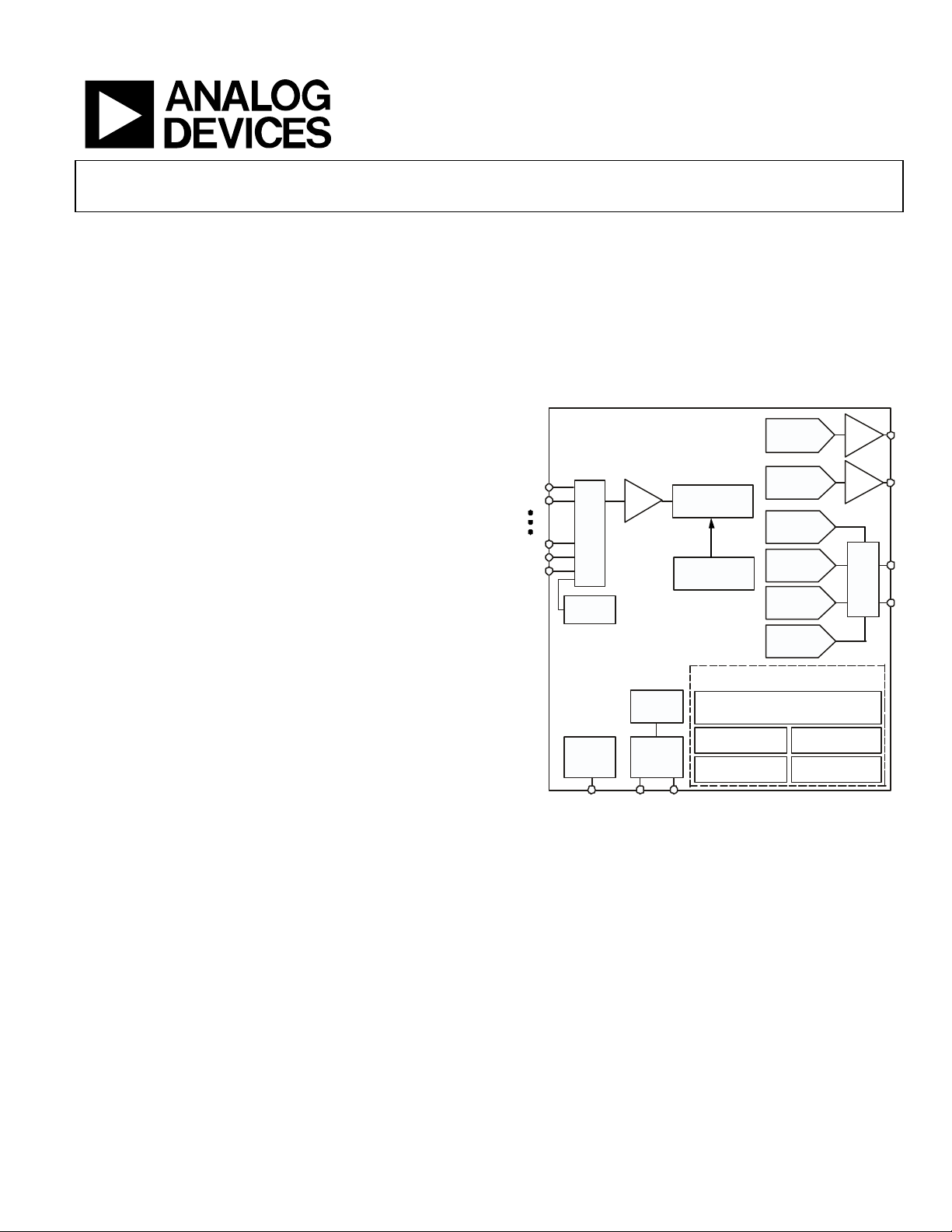
FUNCTIONAL BLOCK DIAGRAM
12-BIT
ADuC841/ADuC842/ADuC 843
ADC0
ADC1
ADC5
ADC6
ADC7
MUX
TEMP
SENSOR
INTERNAL
BAND GAP
VREF
V
REF
T/H
PLL**
OSC
12-BIT ADC
HARDWARE
CALIBRATON
16 MIPS 8051-BASED MCU WITH ADDITIONAL
62 k BYTES FLASH/EE PROGRAM MEMORY
4 k BYTES FLASH/EE DATA MEMORY
2304 BYTES USER RAM
3316 BIT TIMERS
1
3
REAL TIME CLOCK
43 PARALLEL
PORTS
XTAL 2XTAL1
* ADuC841/ADuC842 Only
** ADuC842/ADuC843 Only, ADuC841 driven directly by external crystal.
Purchase of licensed I2C components of Analog Devices or one of its sublicensed
Associated Companies conveys a license for the purchaser under the Philips I
Patent Rights to use these components in an I
conforms to the I
One Technology Way, P.O. Box 9106, Norwood, MA 02062-9106, U.S.A.
2
C Standard Specification as defined by Philips.
Tel: 781.329.4700 www.analog.com
Fax: 781.326.8703 © 2003 Analog Devices, Inc. All rights reserved.
2
C system, provided that the system
DAC
12-BIT
DAC
16-BIT
S- D DAC
16-BIT
S- D DAC
16-BIT
PWM
16-BIT
PWM
PERIPHERALS
POWER SUPPLY MON
WATCHDOG TIMER
UART,I
2
C, AND SPI
SERIAL I/O
BUF
BUF
MUX
DAC*
DAC*
PWM0
PWM1
2
C
 Loading...