

MicroConverter® 12-Bit ADCs and DACs with
Embedded High Speed 62-kB Flash MCU
ADuC841/ADuC842/ADuC843
FEATURES
Pin compatable ugrade of ADuC812/ADuC831/ADuC832
Increased performance
Single-cycle 20 MIPS 8052 core
High speed 420 kSPS 12-bit ADC
Increased memory
Up to 62 kBytes on-chip Flash/EE program memory
4 kBytes on-chip Flash/EE data memory
In-circuit reprogrammable
Flash/EE, 100 year retention, 100 kCycle endurance
2304 bytes on-chip data RAM
Smaller package
8 mm × 8 mm chip scale package
52-lead PQFP—pin compatable upgrade
Analog I/O
8-channel, 420 kSPS high accuracy, 12-bit ADC
On-chip, 15 ppm/°C voltage reference
DMA controller, high speed ADC-to-RAM capture
Two 12-bit voltage output DACs
1
Dual output PWM ∑-∆ DACs
On-chip temperature monitor function
8052 based core
8051 compatible instruction set (20 MHz max)
High performance single-cycle core
32 kHz external crystal, on-chip programmable PLL
12 interrupt sources, 2 priority levels
Dual data pointers, extended 11-bit stack pointer
On-chip peripherals
Time interval counter (TIC)
2
UART, I
C®, and SPI® Serial I/O
Watchdog timer (WDT)
Power supply monitor (PSM)
Power
Normal: 4.5 mA @ 3 V (core CLK = 2.098 MHz)
Power-down: 10 µA @ 3 V
2
Development tools
Low cost, comprehensive development system
incorporating nonintrusive single-pin emulation,
IDE based assembly and C source debugging
APPLICATIONS
Optical networking—laser power control
Base station systems
Precision instrumentation, smart sensors
Transient capture systems
DAS and communications systems
1
ADuC841/ADuC842 only.
2
ADuC842/ADuC843 only, ADuC841 driven directly by external crystal.
ADC0
ADC1
ADC5
ADC6
ADC7
GENERAL DESCRIPTION
The ADuC841/ADuC842/ADuC843 are complete smart
transducer front ends, that integrates a high performance selfcalibrating multichannel ADC, a dual DAC, and an optimized
single-cycle 20 MHz 8-bit MCU (8051 instruction set
compatible) on a single chip.
The ADuC841 and ADuC842 are identical with the exception of
the clock oscillator circuit; the ADuC841 is clocked directly
from an external crystal up to 20 MHz whereas the ADuC842
uses a 32 kHz crystal with an on-chip PLL generating a
programmable core clock up to 16.78 MHz.
The ADuC843 is identical to the ADuC842 except that the
ADuC843 has no analog DAC outputs.
The microcontroller is an optimized 8052 core offering up to
20 MIPS peak performance. Three different memory options
are available offering up to 62 kBytes of nonvolatile Flash/EE
program memory. Four kBytes of nonvolatile Flash/EE data
memory, 256 bytes RAM, and 2 kBytes of extended RAM are
also integrated on-chip.
(continued on page 15)
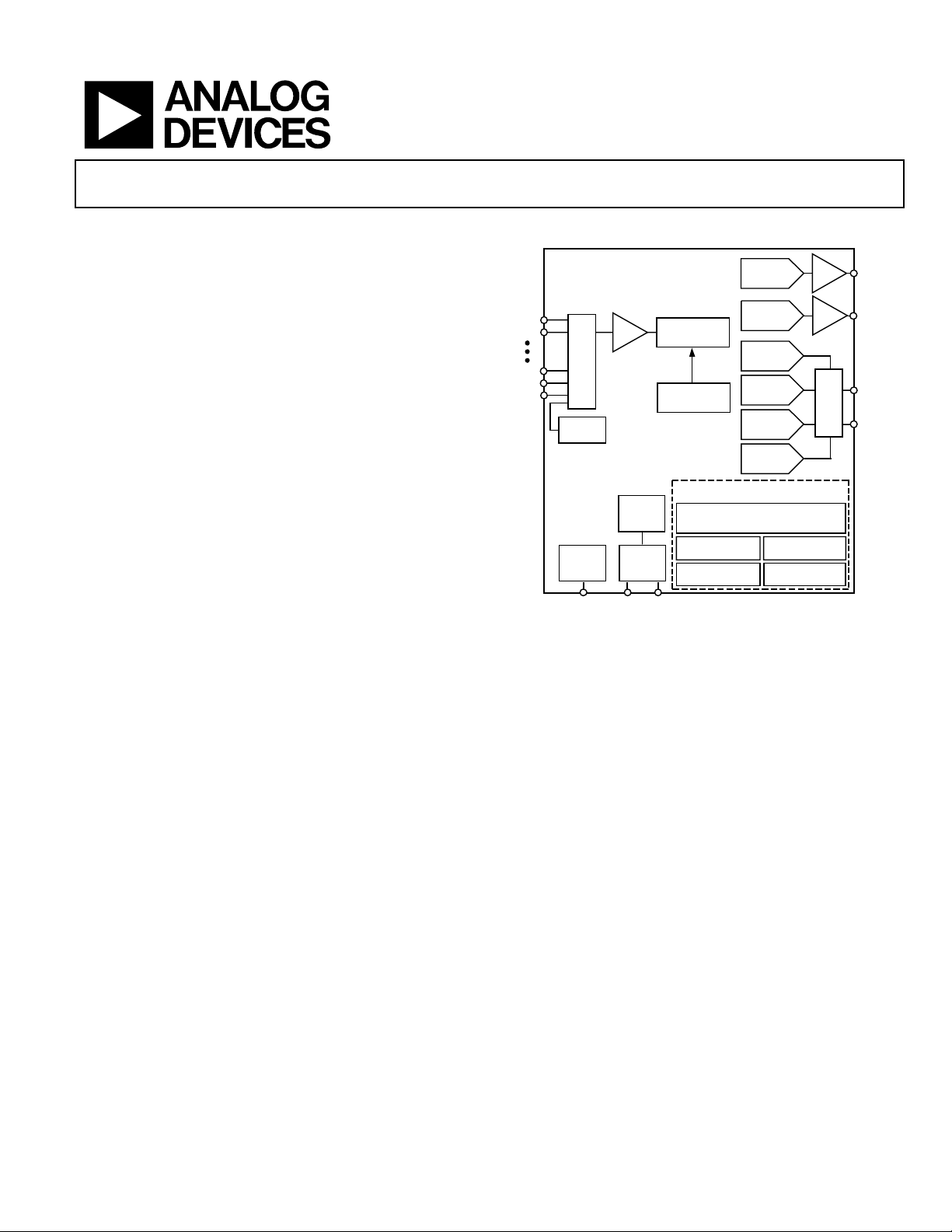
FUNCTIONAL BLOCK DIAGRAM
ADuC841/ADuC842/ADuC843
MUX
TEMP
SENSOR
INTERNAL
BAND GAP
VREF
C
REF
T/H
12-BIT ADC
HARDWARE
CALIBRATON
20 MIPS 8052 BASED MCU WITH ADDITIONAL
62 kBYTES FLASH/EE PROGRAM MEMORY
2
PLL
OSC
XTAL2XTAL1
4 kBYTES FLASH/EE DATA MEMORY
3 × 16 BIT TIMERS
1× REAL TIME CLOCK
4× PARALLEL
PORTS
Figure 1.
12-BIT
12-BIT
16-BIT
Σ-∆ DAC
16-BIT
Σ-∆ DAC
16-BIT
16-BIT
PERIPHERALS
2304 BYTES USER RAM
DAC
DAC
PWM
PWM
POWER SUPPLY MON
WATCHDOG TIMER
2
C, AND SPI
UART, I
SERIAL I/O
BUF
BUF
MUX
DAC
DAC
PWM0
PWM1
1
1
03260-0-001
Rev. 0
Information furnished by Analog Devices is believed to be accurate and reliable.
However, no responsibility is assumed by Analog Devices for its use, nor for any
infringements of patents or other rights of third parties that may result from its use.
Specifications subject to change without notice. No license is granted by implication
or otherwise under any patent or patent rights of Anal og Devices. Trademarks and
registered trademarks are the property of their respective owners.
One Technology Way, P.O. Box 9106, Norwood, MA 02062-9106, U.S.A.
Tel: 781.329.4700 www.analog.com
Fax: 781.326.8703 © 2003 Analog Devices, Inc. All rights reserved.

ADuC841/ADuC842/ADuC843
TABLE OF CONTENTS
Specifications..................................................................................... 3
Absolute Maximum Ratings............................................................ 8
ESD Caution.................................................................................. 8
Pin Configurations and Functional Descriptions........................ 9
Terminology .................................................................................... 11
ADC Specifications ....................................................................11
DAC Specifications..................................................................... 11
Typical Performance Characteristics ........................................... 12
Functional Description.................................................................. 16
8052 Instruction Set ................................................................... 16
Other Single-Cycle Core Features............................................ 18
Memory Organization ............................................................... 19
Special Function Registers (SFRs)............................................ 20
Pulse-Width Modulator (PWM).............................................. 42
Serial Peripheral Interface (SPI)............................................... 45
2
I
C Compatible Interface........................................................... 48
Dual Data Pointer....................................................................... 51
Power Supply Monitor............................................................... 52
Watchdog Timer......................................................................... 53
Time Interval Counter (TIC).................................................... 54
8052 Compatible On-Chip Peripherals................................... 57
Timer/Counter 0 and 1 Operating Modes.............................. 62
Timer/Counter Operating Modes............................................ 64
UART Serial Interface................................................................ 65
SBUF ............................................................................................ 65
Interrupt System......................................................................... 70
Accumulator SFR (ACC)........................................................... 21
Special Function Register Banks ..............................................22
ADC Circuit Information.......................................................... 23
Calibrating the ADC .................................................................. 30
Nonvolatile Flash/EE Memory .................................................31
Using Flash/EE Data Memory .................................................. 34
User Interface to On-Chip Peripherals.................................... 38
On-Chip PLL............................................................................... 41
REVISION HISTORY
Revision 0: Initial Version
Hardware Design Considerations............................................ 72
Other Hardware Considerations.............................................. 76
Development Tools .................................................................... 77
QuickStart Development System ............................................. 77
Timing Specifications
, ,
.................................................................. 78
Outline Dimensions....................................................................... 86
Ordering Guides......................................................................... 87
Rev. 0 | Page 2 of 88

ADuC841/ADuC842/ADuC843
SPECIFICATIONS1
Table 1. AV
all specifications T
Parameter VDD = 5 V VDD = 3 V Unit Test Conditions/Comments
ADC CHANNEL SPECIFICATIONS
DC ACCURACY2, 3
Resolution 12 12 Bits
Integral Nonlinearity ±1 ±1 LSB max 2.5 V internal reference
±0.3 ±0.3 LSB typ
Differential Nonlinearity +1/–0.9 +1/–0.9 LSB max 2.5 V internal reference
±0.3 ±0.3 LSB typ
Integral Nonlinearity4 ±2 ±1.5 LSB max 1 V external reference
Differential Nonlinearity4 +1.5/–0.9 +1.5/–0.9 LSB max 1 V external reference
Code Distribution 1 1 LSB typ ADC input is a dc voltage
CALIBRATED ENDPOINT ERRORS
Offset Error ±3 ±2 LSB max
Offset Error Match ±1 ±1 LSB typ
Gain Error ±3 ±2 LSB max
Gain Error Match ±1 ±1 LSB typ
DYNAMIC PERFORMANCE fIN = 10 kHz sine wave
f
Signal-to-Noise Ratio (SNR)7 71 71 dB typ
Total Harmonic Distortion (THD) –85 –85 dB typ
Peak Harmonic or Spurious Noise –85 –85 dB typ
Channel-to-Channel Crosstalk8 –80 –80 dB typ
ANALOG INPUT
Input Voltage Range 0 to V
Leakage Current ±1 ±1 µA max
Input Capacitance 32 32 pF typ
TEMPERATURE SENSOR9
Voltage Output at 25°C 700 700 mV typ
Voltage TC –1.4 –1.4 mV/°C typ
Accuracy ±1.5 ±1.5 °C typ Internal/External 2.5 V V
DAC CHANNEL SPECIFICATIONS
Internal Buffer Enabled
ADuC841/ADuC842 Only
DC ACCURACY10
Resolution 12 12 Bits
Relative Accuracy ±3 ±3 LSB typ
Differential Nonlinearity11 –1 –1 LSB max Guaranteed 12-bit monotonic
±1/2 ±1/2 LSB typ
Offset Error ±50 ±50 mV max V
Gain Error ±1 ±1 % max AVDD range
±1 ±1 % typ V
Gain Error Mismatch 0.5 0.5 % typ % of full-scale on DAC1
ANALOG OUTPUTS
Voltage Range_0 0 to V
Voltage Range_1 0 to VDD 0 to VDD V typ DAC V
Output Impedance 0.5 0.5 Ω typ
= DVDD = 2.7 V to 3.6 V or 4.75 V to 5.25 V; V
DD
= T
to T
A
MIN
, unless otherwise noted
MAX
5, 6
0 to V
REF
DAC load to AGND
R
0 to V
REF
= 2.5 V internal reference, f
REF
V
REF
V typ DAC V
REF
= 16.78 MHz @ 5 V 8.38 MHz @ 3 V;
CORE
= 120 kHz, see the Typical
f
SAMPLE
Performance Characteristics for typical
performance at other values of f
= 120 kHz
SAMPLE
REF
= 10 kΩ, CL = 100 pF
L
SAMPLE
range
REF
range
REF
= 2.5 V
REF
= VDD
REF
Rev. 0 | Page 3 of 88
ADuC841/ADuC842/ADuC843
Parameter VDD = 5 V VDD = 3 V Unit Test Conditions/Comments
DAC AC CHARACTERISTICS
Voltage Output Settling Time 15 15 µs typ
Digital-to-Analog Glitch Energy 10 10 nV-sec typ 1 LSB change at major carry
DAC CHANNEL SPECIFICATIONS
12, 13
Internal Buffer Disabled ADuC841/ADuC842 Only
DC ACCURACY10
Resolution 12 12 Bits
Relative Accuracy ±3 ±3 LSB typ
Differential Nonlinearity11 –1 –1 LSB max Guaranteed 12-bit monotonic
±1/2 ±1/2 LSB typ
Offset Error ±5 ±5 mV max V
Gain Error ±0.5 ±0.5 % typ V
Gain Error Mismatch4 0.5 0.5 % typ % of full-scale on DAC1
ANALOG OUTPUTS
Voltage Range_0 0 to V
0 to V
REF
V typ DAC V
REF
REFERENCE INPUT/OUTPUT REFERENCE OUTPUT14
Output Voltage (V
) 2.5 2.5 V
REF
Accuracy ±10 ±10 mV Max
Power Supply Rejection 65 67 dB typ
Reference Temperature Coefficient ±15 ±15 ppm/°C typ
Internal V
Power-On Time 2 2 ms typ
REF
EXTERNAL REFERENCE INPUT15
Voltage Range (V
V
) 4 1 1 V min
REF
V
DD
V max
DD
Input Impedance 20 20 kΩ typ
Input Leakage 1 1 µA max
POWER SUPPLY MONITOR (PSM)
DVDD Trip Point Selection Range
2.93
3.08
V min
V max
DVDD Power Supply Trip Point Accuracy ±2.5 % max
WATCHDOG TIMER (WDT) 4
Timeout Period 0
2000
0
2000
ms min
ms max
FLASH/EE MEMORY RELIABILITY CHARACTERISTICS16
Endurance17 100,000 100,000 Cycles min
Data Retention18 100 100 Years min
DIGITAL INPUTS
Input Leakage Current (Port 0, EA)
±10 ±10 µA max V
±1 ±1 µA typ VIN = 0 V or VDD
Logic 1 Input Current
(All Digital Inputs), SDATA, SCLOCK ±10 ±10 µA max VIN = VDD
±1 ±1 µA typ VIN = VDD
Logic 0 Input Current (Ports 1, 2, 3) SDATA, SCLOCK –75 –25 µA max
–40 –15 µA typ VIL = 450 mV
Logic 1 to Logic 0 Transition Current (Ports 2 and 3) –660 –250 µA max VIL = 2 V
RESET
–400
±10
10
105
–140
±10
5
35
µA typ
µA max
µA min
µA max
Full-scale settling time to within
½ LSB of final value
range
REF
range
REF
= 2.5 V
REF
measured at the C
Of V
= 25°C
T
A
REF
REF
Internal band gap deselected via
ADCCON1.6
Two trip points selectable in this
range programmed via TPD1–0 in
PSMCON, 3 V part only
Nine timeout periods selectable in
this range
= 0 V or VDD
IN
V
= 2 V
IL
V
= 0 V
IN
V
= 5 V, 3 V Internal Pull Down
IN
V
= 5 V, 3 V Internal Pull Down
IN
pin
Rev. 0 | Page 4 of 88
ADuC841/ADuC842/ADuC843
Parameter VDD = 5 V VDD = 3 V Unit Test Conditions/Comments
LOGIC INPUTS
INPUT VOLTAGES
All Inputs Except SCLOCK, SDATA, RESET, and
XTAL1
VINL, Input Low Voltage
VINH, Input High Voltage
SDATA
VINL, Input Low Voltage
VINH, Input High Voltage
SCLOCK and RESET Only
(Schmitt-Triggered Inputs)
V
T+
V
T–
V
T+
CRYSTAL OSCILLATOR
Logic Inputs, XTAL1 Only
V
INL
V
INH
XTAL1 Input Capacitance 18 18 pF typ
XTAL2 Output Capacitance 18 18 pF typ
MCU CLOCK RATE 16.78
DIGITAL OUTPUTS
Output High Voltage (VOH) 2.4 V min VDD = 4.5 V to 5.5 V
4 V typ I
2.4 V min VDD = 2.7 V to 3.3 V
2.6 V typ I
Output Low Voltage (VOL)
ALE, Ports 0 and 2 0.4 0.4 V max I
0.2 0.2 V typ I
Port 3 0.4 0.4 V max I
SCLOCK/SDATA 0.4 0.4 V max I
Floating State Leakage Current4 ±10 ±10 µA max
±1 ±1 µA typ
STARTUP TIME At any core CLK
At Power-On 500 500 ms typ
From Idle Mode 100 100 µs typ
From Power-Down Mode
4
0.8
2.0
0.8
2.0
0.4
2.0
0.8
2.0
V max
V min
V max
V min
– VT–
4
1.3
3.0
0.8
1.4
0.3
0.85
0.95
0.25
0.4
1.1
0.3
0.85
V min
V max
V min
V max
V min
V max
, Input Low Voltage 0.8 0.4 V typ
, Input High Voltage 3.5 2.5 V typ
Wake-up with
INT0
Interrupt
8.38
20
8.38
150 400 µs typ
MHz max
MHz max
ADuC842/ADuC843 Only
ADuC841 Only
= 80 µA
SOURCE
= 20 µA
SOURCE
= 1.6 mA
SINK
= 1.6 mA
SINK
= 4 mA
SINK
= 8 mA, I2C Enabled
SINK
Wake-up with SPI/I2C Interrupt 150 400 µs typ
Wake-up with External RESET 150 400 µs typ
After External RESET in Normal Mode 30 30 ms typ
After WDT Reset in Normal Mode 3 3 ms typ Controlled via WDCON SFR
Rev. 0 | Page 5 of 88

ADuC841/ADuC842/ADuC843
Parameter VDD = 5 V VDD = 3 V Unit Test Conditions/Comments
POWER REQUIREMENTS
Power Supply Voltages
AVDD/DVDD – AGND 2.7 V min AVDD/DVDD = 3 V nom
3.6 V max
4.75 V min AVDD/DVDD = 5 V nom
5.25 V max
Power Supply Currents Normal Mode21
DVDD Current4 10 4.5 mA typ Core CLK = 2.097 MHz
AVDD Current 1.7 1.7 mA max Core CLK = 2.097 MHz
DVDD Current 38 12 mA max Core CLK = 16.78MHz/8.38 MHz 5 V/3 V
33 10 mA typ Core CLK = 16.78MHz/8.38 MHz 5 V/3 V
AVDD Current 1.7 1.7 mA max Core CLK = 16.78MHz/8.38 MHz 5 V/3 V
DVDD Current4
Power Supply Currents Idle Mode
DVDD Current 4.5 2.2 mA typ Core CLK = 2.097 MHz
AVDD Current 3 2 µA typ Core CLK = 2.097 MHz
DVDD Current4 12 5 mA max Core CLK = 16.78MHz/8.38 MHz 5 V/3 V
10 3.5 mA typ Core CLK = 16.78MHz/8.38 MHz 5 V/3 V
AVDD Current 3 2 µA typ Core CLK = 16.78MHz/8.38 MHz 5 V/3 V
Power Supply Currents Power-Down Mode21
DVDD Current 28
AVDD Current 2 1 µA typ Core CLK = any frequency
DVDD Current4 3 1 mA max TIMECON.1 = 1
DVDD Current4 50
Typical Additional Power Supply Currents
PSM Peripheral 15 10 µA typ AVDD = DVDD
ADC4 1.0
DAC 150 130 µA typ
See footnotes on the next page.
19, 20
21
45 N/A mA max
Core CLK = 20MHz ADuC841 Only
Core CLK = any frequency
20
18
10
µA max
µA typ
Oscillator Off / TIMECON.1 = 0
ADuC841 Only
40
22
15
µA max
µA typ
Core CLK = any frequency
ADuC842/ADuC843 Only
Oscillator On
2.8
1.0
1.8
mA min
mA max
MCLK Divider = 32
MCLK Divider = 2
Rev. 0 | Page 6 of 88

ADuC841/ADuC842/ADuC843
1
Temperature Range –40°C to +85°C.
2
ADC linearity is guaranteed during normal MicroConverter core operation.
3
ADC LSB size = V
4
These numbers are not production tested but are supported by design and/or characterization data on production release.
5
Offset and gain error and offset and gain error match are measured after factory calibration.
6
Based on external ADC system components, the user may need to execute a system calibration to remove additional external channel errors to achieve these
specifications.
7
SNR calculation includes distortion and noise components.
8
Channel-to-channel crosstalk is measured on adjacent channels.
9
The temperature monitor gives a measure of the die temperature directly; air temperature can be inferred from this result.
10
DAC linearity is calculated using:
Reduced code range of 100 to 4095, 0 V to V
Reduced code range of 100 to 3945, 0 V to VDD range.
DAC output load = 10 kΩ and 100 pF.
11
DAC differential nonlinearity specified on 0 V to V
12
DAC specification for output impedance in the unbuffered case depends on DAC code.
13
DAC specifications for I
unbuffered mode tested with OP270 external buffer, which has a low input leakage current.
14
Measured with C
chosen for the C
15
When using an external reference device, the internal band gap reference input can be bypassed by setting the ADCCON1.6 bit.
16
Flash/EE memory reliability characteristics apply to both the Flash/EE program memory and the Flash/EE data memory.
17
Endurance is qualified to 100,000 cycles as per JEDEC Std. 22 method A117 and measured at –40°C, +25°C, and +85°C. Typical endurance at 25°C is 700,000 cycles.
18
Retention lifetime equivalent at junction temperature (TJ) = 55°C as per JEDEC Std. 22 method A117. Retention lifetime based on an activation energy of 0.6 eV derates
with junction temperature as shown in Figure 38 in the Flash/EE Memory Reliability section.
19
Power supply current consumption is measured in normal, idle, and power-down modes under the following conditions:
Normal Mode: Reset = 0.4 V, digital I/O pins = open circuit, Core Clk changed via CD bits in PLLCON (ADuC842/ADuC843), core executing internal
Idle Mode: Reset = 0.4 V, digital I/O pins = open circuit, Core Clk changed via CD bits in PLLCON (ADuC842/ADuC843), PCON.0 = 1, core execution
Power-Down Mode: Reset = 0.4 V, all Port 0 pins = 0.4 V, All other digital I/O and Port 1 pins are open circuit, Core Clk changed via CD bits in PLLCON
20
DVDD power supply current increases typically by 3 mA (3 V operation) and 10 mA (5 V operation) during a Flash/EE memory program or erase cycle.
21
Power supply currents are production tested at 5.25 V and 3.3 V for a 5 V and 3 V part, respectively.
/212, i.e., for internal V
REF
, voltage output settling time, and digital-to-analog glitch energy depend on external buffer implementation in unbuffered mode. DAC in
SINK
pin decoupled with 0.47 µF capacitor to ground. Power-up time for the internal reference is determined by the value of the decoupling capacitor
REF
pin.
REF
= 2.5 V, 1 LSB = 610 µV, and for external V
REF
range.
REF
and 0 V to VDD ranges.
REF
= 1 V, 1 LSB = 244 µV.
REF
software loop.
suspended in idle mode.
(ADuC842/ADuC843), PCON.0 = 1, core execution suspended in power-down mode, OSC turned on or off via OSC_PD bit (PLLCON.7) in
PLLCON SFR (ADuC842/ADuC843).
Rev. 0 | Page 7 of 88
ADuC841/ADuC842/ADuC843
A
A
A
A
ABSOLUTE MAXIMUM RATINGS
Table 2. TA = 25°C, unless otherwise noted
Parameter Rating
AVDD to DVDD –0.3 V to +0.3 V
AGND to DGND –0.3 V to +0.3 V
DVDD to DGND, AVDD to AGND –0.3 V to +7 V
Digital Input Voltage to DGND –0.3 V to DVDD + 0.3 V
Digital Output Voltage to DGND –0.3 V to DVDD + 0.3 V
V
to AGND –0.3 V to AVDD + 0.3 V
REF
Analog Inputs to AGND –0.3 V to AVDD + 0.3 V
Operating Temperature Range,
Industrial
–40°C to +85°C
ADuC841BS,ADuC842BS,ADuC843BS
ADuC841BCP, ADuC842BCP,
ADuC843BCP
Storage Temperature Range –65°C to +150°C
Junction Temperature 150°C
θJA Thermal Impedance (ADuC84xBS) 90°C/W
θJA Thermal Impedance (ADuC84xBCP) 52°C/W
Lead Temperature, Soldering
Vapor Phase (60 sec)
Infrared (15 sec)
215°C
220°C
ESD CAUTION
ESD (electrostatic discharge) sensitive device. Electrostatic charges as high as 4000 V readily accumulate on the
human body and test equipment and can discharge without detection. Although this product features
proprietary ESD protection circuitry, permanent damage may occur on devices subjected to high energy
electrostatic discharges. Therefore, proper ESD precautions are recommended to avoid performance
degradation or loss of functionality.
ADuC841/ADuC842/ADuC843
C
DC0
DC1
DC6
DC7
REF
...
TEMP
SENSOR
DD
AV
MUX
BAND GAP
REFERENCE
DDDVDDDVDD
DV
AGND
...
BUF
T/H
POR
DGND
DGND
Figure 2. ADuC Block Diagram (Shaded Areas are Features Not Present on the ADuC812),
No DACs on ADuC843, PLL on ADuC842/ADuC843 Only.
12-BIT
ADC
62 kBYTES PROGRAM
FLASH/EE INCLUDING
USER DOWNLOAD
MODE
4 kBYTES DATA
FLASH/EE
2 kBYTES USER XRAM
2 × DATA POINTERS
11-BIT STACK POINTER
DOWNLOADER
DEBUGGER
ASYNCHRONOUS
SERIAL PORT
(UART)
RESET
RxD
DGND
TxD
Rev. 0 | Page 8 of 88
Stresses above those listed under Absolute Maximum Ratings
may cause permanent damage to the device. This is a stress
rating only and functional operation of the device at these or
any other conditions above those indicated in the operational
section of this specification is not implied. Exposure to absolute
maximum rating conditions for extended periods may affect
device reliability.
ADC
CONTROL
AND
CALIBRATION
UART
TIMER
8052
MCU
CORE
ALE
EMULATOR
SINGLE-PIN
EA
PSEN
CONTROL
DAC
CONTROL
256 BYTES USER
WATCHDOG
POWER SUPPLY
SYNCHRONOUS
SERIAL INTERFACE
2
(I
C AND SPI )
SCLOCK
OUTPUT DAC
OUTPUT DAC
PWM
RAM
TIMER
MONITOR
TIME INTERVAL
(WAKE-UP CCT)
SS
MISO
SDATA\MOSI
12-BIT
VOLTAGE
12-BIT
VOLTAGE
16-BIT
Σ-∆ DAC
16-BIT
Σ-∆ DAC
16-BIT
16-BIT
COUNTER
PWM
PWM
16-BIT
COUNTER
TIMERS
PLL
OSC
XTAL1
DAC0
DAC1
PWM0
MUX
PWM1
T0
T1
T2
T2EX
INT0
INT1
03260-0-002
XTAL2
ADuC841/ADuC842/ADuC843
0
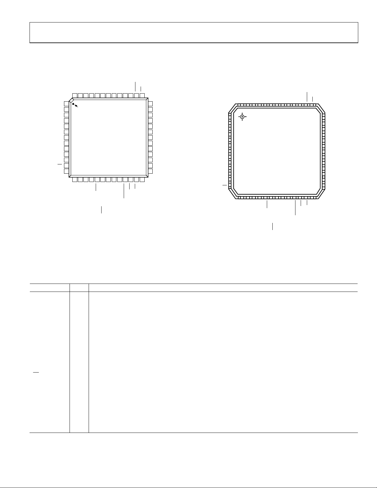
PIN CONFIGURATIONS AND FUNCTIONAL DESCRIPTIONS
ALE
PSEN
P0.7/AD7P0.6/AD6P0.5/AD5P0.4/AD4DVDDDGND
52 51 50 49 48 43 42 41 4047 46 45 44
AV
AGND
C
REF
V
REF
DAC0
DAC1
1
PIN 1
2
IDENTIFIER
3
4
5
DD
ADuC841/ADuC842/ADuC843
6
7
8
9
10
11
12
13
52-LEAD PQFP
14 15 16 17 18 19 20 21 22 23 24 25 26
RESET
P3.0/RXD
P1.7/ADC7
P1.0/ADC0/T2
P1.1/ADC1/T2EX
P1.2/ADC2
P1.3/ADC3
P1.4/ADC4
P1.5/ADC5/SS
P1.6/ADC6
*EXTCLK NOT PRESENT ON THE ADuC841
TOP VIEW
(Not to Scale)
P3.1/TXD
P3.2/INT0
P3.3/INT1/MISO/PWM1
P0.3/AD3P0.2/AD2P0.1/AD1
DD
DV
DGND
P3.4/T0/PWMC/PWM0/EXTCLK*
Figure 3. 52-Lead PQPF
Table 3. Pin Function Descriptions
Mnemonic Type Function
DVDD P Digital Positive Supply Voltage. 3 V or 5 V nominal.
AVDD P Analog Positive Supply Voltage. 3 V or 5 V nominal.
C
I/O Decoupling Input for On-Chip Reference. Connect a 0.47 µF capacitor between this pin and AGND.
REF
V
NC Not connected. This was reference out on the ADuC812; the C
REF
AGND G Analog Ground. Ground reference point for the analog circuitry.
P1.0–P1.7 I
Port 1 is an 8-bit input port only. Unlike other ports, Port 1 defaults to analog input mode. To configure any of
these port pins as a digital input, write a 0 to the port bit.
ADC0–ADC7 I Analog Inputs. Eight single-ended analog inputs. Channel selection is via ADCCON2 SFR.
T2 I
Timer 2 Digital Input. Input to Timer/Counter 2. When enabled, Counter 2 is incremented in response to a 1-to-0
transition of the T2 input.
T2EX I Digital Input. Capture/reload trigger for Counter 2; also functions as an up/down control input for Counter 2.
SS
I Slave Select Input for the SPI Interface.
SDATA I/O User Selectable, I2C Compatible, or SPI Data Input/Output Pin.
SCLOCK I/O Serial Clock Pin for I2C Compatible or for SPI Serial Interface Clock.
MOSI I/O SPI Master Output/Slave Input Data I/O Pin for SPI Interface.
MISO I/O SPI Master Input/Slave Output Data I/O Pin for SPI Serial Interface.
DAC0 O Voltage Output from DAC0. This pin is a no connect on the ADuC843.
DAC1 O Voltage Output from DAC1. This pin is a no connect on the ADuC843.
RESET I Digital Input. A high level on this pin for 24 master clock cycles while the oscillator is running resets the device.
P0.0/AD
P3.6/WR
P3.5/T1/CONVST
EA
39
38
37
36
35
34
33
32
31
30
29
28
27
P3.7/RD
SCLOCK
P2.7/PWM1/A15/A23
P2.6/PWM0/A14/A22
P2.5/A13/A21
P2.4/A12/A20
DGND
DV
DD
XTAL2
XTAL1
P2.3/A11/A19
P2.2/A10/A18
P2.1/A9/A17
P2.0/A8/A16
SDATA/MOSI
P1.0/ADC0/T2
P0.7/AD7
55
P1.1/ADC1/T2EX
P1.2/ADC2
P1.3/ADC3
AV
AV
AGND
AGND
AGND
C
REF
V
REF
DAC0
DAC1
P1.4/ADC4
P1.5/ADC5/SS
03260-0-003
*EXTCLK NOT PRESENT ON THE ADuC841
56
1
2
PIN 1
IDENTIFIER
3
4
DD
5
DD
6
ADuC841/ADuC842/ADuC843
7
8
9
10
11
12
13
14
15161718192021222324252627
P.7/ADC7
P1.6/ADC6
pin should be used instead.
REF
DD
DV
P0.6/AD6
P0.5/AD5
DGND
P0.4/AD4
P0.3/AD3
51
49
50
52
53
54
56-LEAD CSP
TOP VIEW
(Not to Scale)
DD
P3.1/TxD
P3.2/INT0
DV
P3.3/INT1/MISO/PWM1
RESET
P3.0/RxD
Figure 4. 56-Lead CSP
P0.2/AD2
P0.1/AD1
47
48
DGND
P3.4/T0/PWMC/PWM0/EXTCLK*
ALE
P0.0/AD0
45
46
P3.6/WR
P3.5/T1/CONVST
PSEN
43
44
42
41
40
39
38
37
36
35
34
33
32
31
30
29
28
P3.7/RD
EA
SCLOCK
P2.7/A15/A23
P2.6/A14/A22
P2.5/A13/A21
P2.4/A12/A20
DGND
DGND
DV
DD
XTAL2
XTAL1
P2.3/A11/A19
P2.2/A10/A18
P2.1/A9/A17
P2.0/A8/A16
SDATA/MOSI
03260-0-004
Rev. 0 | Page 9 of 88

ADuC841/ADuC842/ADuC843
Mnemonic Type Function
P3.0–P3.7 I/O
PWMC I PWM Clock Input.
PWM0 O PWM0 Voltage Output. PWM outputs can be configured to use Ports 2.6 and 2.7 or Ports 3.4 and 3.3.
PWM1 O PWM1 Voltage Output. See the CFG841/CFG842 register for further information.
RxD I/O Receiver Data Input (Asynchronous) or Data Input/Output (Synchronous) of the Serial (UART) Port.
TxD O Transmitter Data Output (Asynchronous) or Clock Output (Synchronous) of the Serial (UART) Port.
INT0
INT1
T0 I Timer/Counter 0 Input.
T1 I Timer/Counter 1 Input.
CONVST
EXTCLK I Input for External Clock Signal. Has to be enabled via the CFG842 register.
WR
RD
XTAL2 O Output of the Inverting Oscillator Amplifier.
XTAL1 I Input to the Inverting Oscillator Amplifier.
DGND G Digital Ground. Ground reference point for the digital circuitry.
P2.0–P2.7
(A8–A15)
(A16–A23)
PSEN
ALE O
EA
P0.7–P0.0
(A0-A7)
Types: P = Power, G = Ground, I= Input, O = Output., NC = No Connect
I
I
I
O Write Control Signal, Logic Output. Latches the data byte from Port 0 into the external data memory.
O Read Control Signal, Logic Output. Enables the external data memory to Port 0.
I/O
O
I
I/O
Port 3 is a bidirectional port with internal pull-up resistors. Port 3 pins that have 1s written to them are pulled high
by the internal pull-up resistors, and in that state can be used as inputs. As inputs, Port 3 pins being pulled
externally low source current because of the internal pull-up resistors. Port 3 pins also contain various secondary
functions, which are described below.
Interrupt 0. Programmable edge or level triggered interrupt input; can be programmed to one of two priority
levels. This pin can also be used as a gate control input to Timer 0.
Interrupt 1. Programmable edge or level triggered interrupt input; can be programmed to one of two priority
levels. This pin can also be used as a gate control input to Timer 1.
Active Low Convert Start Logic Input for the ADC Block when the External Convert Start Function is Enabled. A
low-to-high transition on this input puts the track-and-hold into hold mode and starts the conversion.
Port 2 is a bidirectional port with internal pull-up resistors. Port 2 pins that have 1s written to them are pulled high
by the internal pull-up resistors, and in that state can be used as inputs. As inputs, Port 2 pins being pulled
externally low source current because of the internal pull-up resistors. Port 2 emits the middle and high-order
address bytes during accesses to the external 24-bit external data memory space.
Program Store Enable, Logic Output. This pin remains low during internal program execution.
enable serial download mode when pulled low through a resistor on power-up or reset. On reset this pin will
momentarily become an input and the status of the pin is sampled. If there is no pulldown resistor in place the pin
will go momentarilly high and then user code will execute. If a pull-down resistor is in place, the embedded serial
download/debug kernel will execute.
Address Latch Enable, Logic Output. This output is used to latch the low byte and page byte for 24-bit address
space accesses of the address into external data memory.
External Access Enable, Logic Input. When held high, this input enables the device to fetch code from internal
program memory locations. The parts do not support external code memory. This pin should not be left floating.
Port 0 is an 8-bit open-drain bidirectional I/O port. Port 0 pins that have 1s written to them float, and in that state
can be used as high impedance inputs. Port 0 is also the multiplexed low-order address and data bus during
accesses to external data memory. In this application, it uses strong internal pull-ups when emitting 1s.
PSEN
is used to
Rev. 0 | Page 10 of 88

ADuC841/ADuC842/ADuC843
TERMINOLOGY
ADC SPECIFICATIONS
Integral Nonlinearity
The maximum deviation of any code from a straight line
passing through the endpoints of the ADC transfer function.
The endpoints of the transfer function are zero scale, a point
½ LSB below the first code transition, and full scale, a point
½ LSB above the last code transition.
Differential Nonlinearity
The difference between the measured and the ideal 1 LSB
change between any two adjacent codes in the ADC.
Offset Error
The deviation of the first code transition (0000 . . . 000) to
(0000 . . . 001) from the ideal, i.e., +½ LSB.
Gain Error
The deviation of the last code transition from the ideal AIN
voltage (Full Scale – ½ LSB) after the offset error has been
adjusted out.
DAC SPECIFICATIONS
Relative Accuracy
Relative accuracy or endpoint linearity is a measure of the
maximum deviation from a straight line passing through the
endpoints of the DAC transfer function. It is measured after
adjusting for zero error and full-scale error.
Voltage Output Settling Time
The amount of time it takes for the output to settle to a
specified level for a full-scale input change.
Digital-to-Analog Glitch Impulse
The amount of charge injected into the analog output when the
inputs change state. It is specified as the area of the glitch in nV-sec.
Signal-to-(Noise + Distortion) Ratio
The measured ratio of signal to (noise + distortion) at the
output of the ADC. The signal is the rms amplitude of the
fundamental. Noise is the rms sum of all nonfundamental
signals up to half the sampling frequency (f
The ratio depends on the number of quantization levels in the
digitization process; the more levels, the smaller the quantization
noise. The theoretical signal-to-(noise + distortion) ratio for an
ideal N-bit converter with a sine wave input is given by
Signal-to-(Noise + Distortion) = (6.02N + 1.76) dB
Thus for a 12-bit converter, this is 74 dB.
Total Harmonic Distortion (THD)
The ratio of the rms sum of the harmonics to the fundamental.
/2), excluding dc.
S
Rev. 0 | Page 11 of 88
ADuC841/ADuC842/ADuC843
TYPICAL PERFORMANCE CHARACTERISTICS
The typical performance plots presented in this section
illustrate typical performance of the ADuC841/ADuC842/
ADuC843 under various operating conditions.
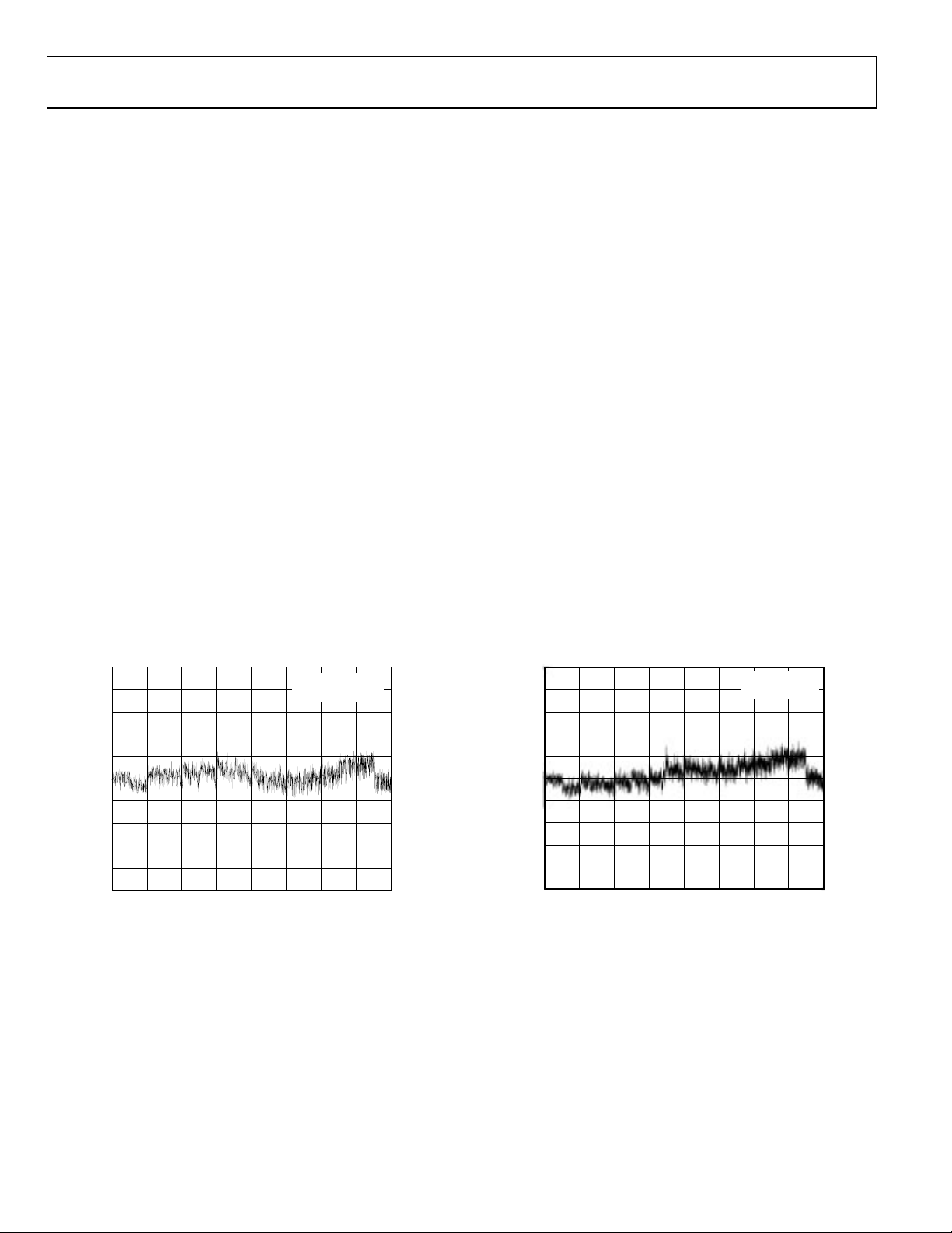
Figure 5 and Figure 6 show typical ADC integral nonlinearity
(INL) errors from ADC Code 0 to Code 4095 at 5 V and 3 V
supplies, respectively. The ADC is using its internal reference
(2.5 V) and is operating at a sampling rate of 152 kHz; the
typical worst-case errors in both plots are just less than 0.3 LSB.
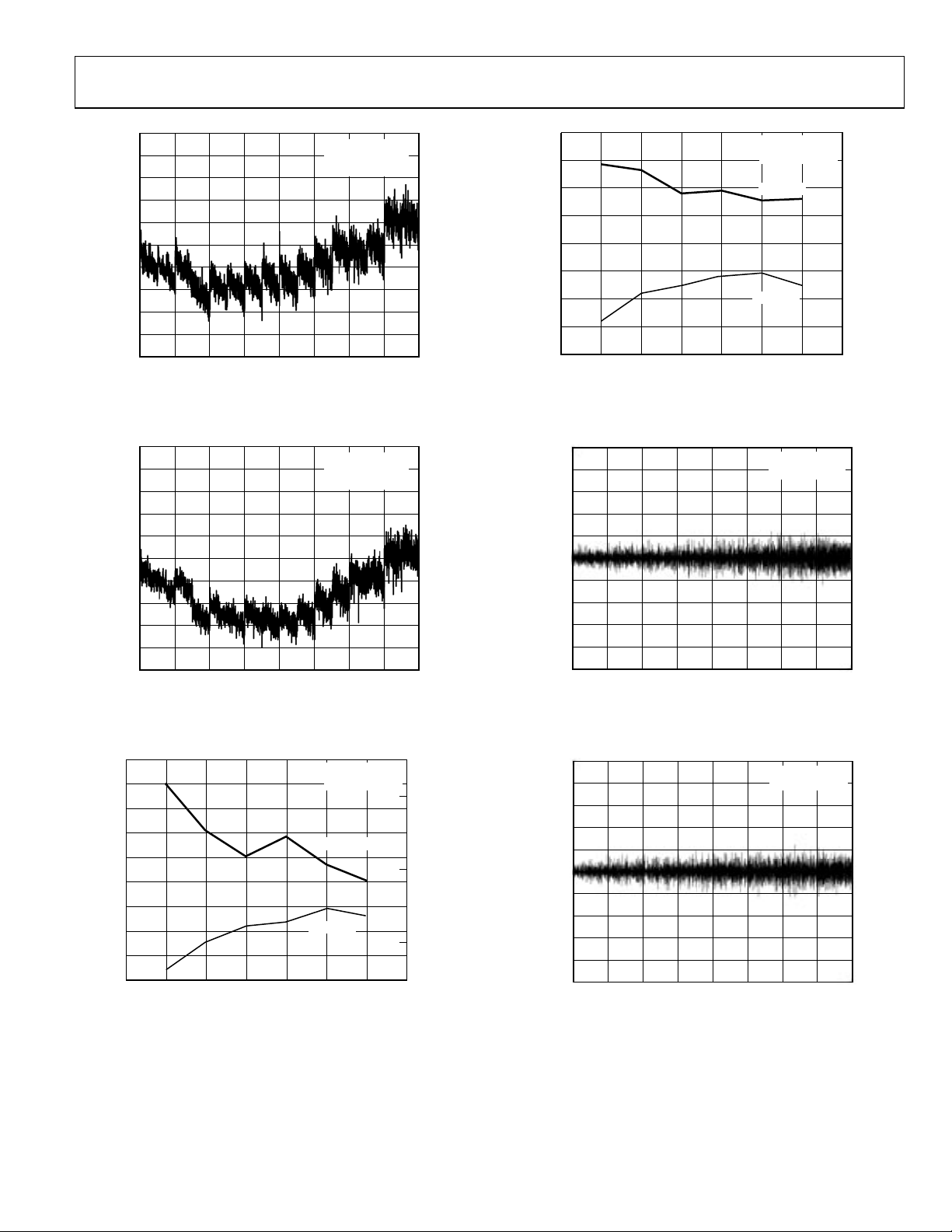
Figure 7 and Figure 8 also show ADC INL at a higher sampling
rate of 400 kHz. Figure 9 and Figure 10 show the variation in
worst-case positive (WCP) INL and worst-case negative (WCN)
INL versus external reference input voltage.
Figure 11 and Figure 12 show typical ADC differential
nonlinearity (DNL) errors from ADC Code 0 to Code 4095 at
5 V and 3 V supplies, respectively. The ADC is using its internal
reference (2.5 V) and is operating at a sampling rate of 152 kHz;
the typical worst-case errors in both plots are just less than
0.2 LSB. Figure 13 and Figure 14 show the variation in worstcase positive (WCP) DNL and worst-case negative (WCN) DNL
versus external reference input voltage.
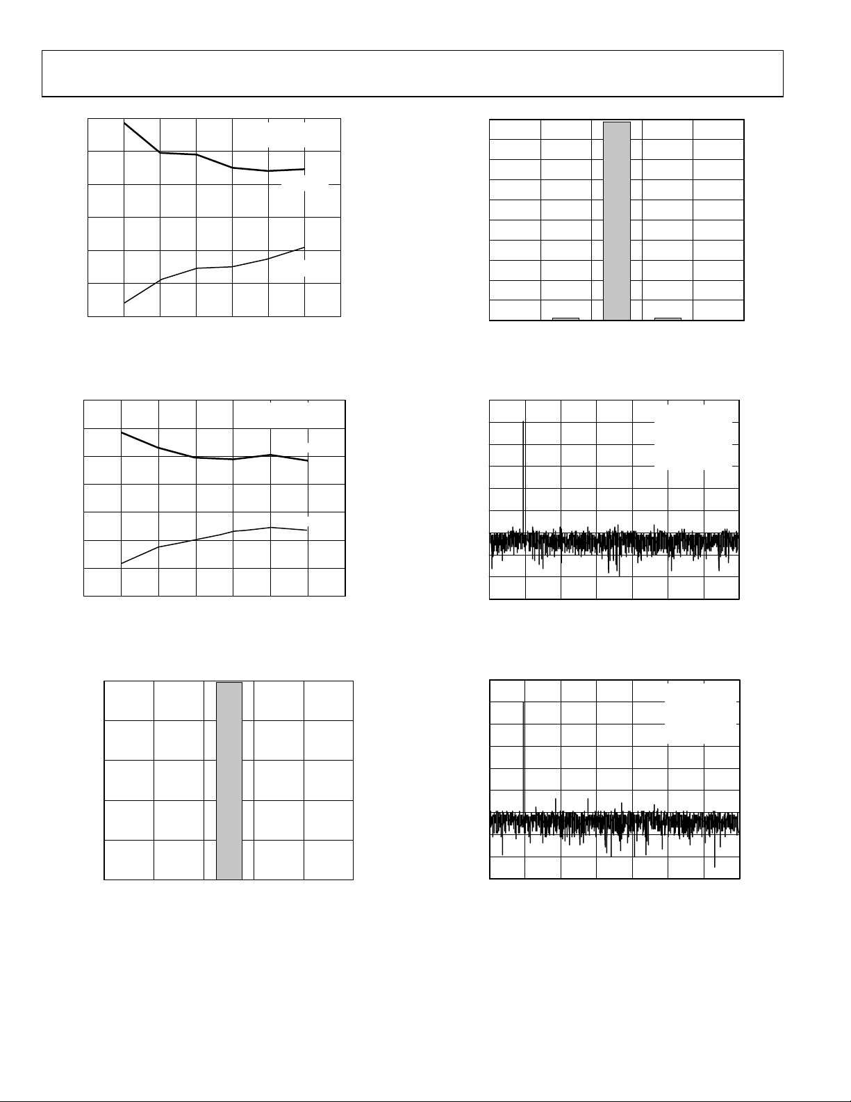
Figure 15 shows a histogram plot of 10,000 ADC conversion
results on a dc input with V
excellent code distribution pointing to the low noise
performance of the on-chip precision ADC.
1.0
0.8
0.6
0.4
0.2
0
LSBs
–0.2
–0.4
–0.6
–0.8
–1.0
0 511
1023 2047 2559 3071
Figure 5. Typical I NL Error, V
= 5 V. The plot illustrates an
DD
AVDD / DVDD = 5V
f
= 152kHz
S
1535 3583
ADC CODES
= 5 V, fs = 152 kHz
DD
4095
03260-0-005
Figure 16 shows a histogram plot of 10,000 ADC conversion
results on a dc input for V
= 3 V. The plot again illustrates a
DD
very tight code distribution of 1 LSB with the majority of codes
appearing in one output pin.
Figure 17 and Figure 18 show typical FFT plots for the parts.
These plots were generated using an external clock input. The
ADC is using its internal reference (2.5 V), sampling a full-scale,
10 kHz sine wave test tone input at a sampling rate of 149.79 kHz.
The resulting FFTs shown at 5 V and 3 V supplies illustrate an
excellent 100 dB noise floor, 71 dB signal-to-noise ratio (SNR),
and THD greater than –80 dB.
Figure 19 and Figure 20 show typical dynamic performance
versus external reference voltages. Again, excellent ac performance can be observed in both plots with some roll-off being
observed as V
falls below 1 V.
REF
Figure 21 shows typical dynamic performance versus sampling
frequency. SNR levels of 71 dB are obtained across the sampling
range of the parts.
Figure 22 shows the voltage output of the on-chip temperature
sensor versus temperature. Although the initial voltage output at
25°C can vary from part to part, the resulting slope of −1. 4 mV/°C
is constant across all parts.
1.0
0.8
0.6
0.4
0.2
0
LSBs
–0.2
–0.4
–0.6
–0.8
–1.0
511 1023 1535 2047 2559
Figure 6. Typical I NL Error, V
ADC CODES
DD
AVDD/DVDD = 3V
f
= 152kHz
S
3071 35830 4095
= 3 V, fs = 152 kHz
03260-0-006
Rev. 0 | Page 12 of 88
ADuC841/ADuC842/ADuC843
1.0
0.8
0.6
0.4
0.2
0
LSBs
–0.2
–0.4
–0.6
–0.8
–1.0
0 511
Figure 7. Typical I NL Error, V
AV
DD
f
= 400kHz
S
CD = 4
1023 2047 2559 3071
1535 3583
ADC CODES
= 5 V, fS = 400 kHz
DD
/DV
0.8
= 5V
DD
4095
03260-0-098
0.6
0.4
0.2
(LSBs)
0
–0.2
WCP–INL
–0.4
–0.6
–0.8
0.5 1.5 2.5
EXTERNAL REFERENCE (V)
Figure 10. Typical Worst-Case INL Error vs. V
AVDD/DVDD = 3V
f
= 152kHz
S
WCP INL
WCN INL
3.02.01.0
, VDD = 3 V
REF
0.8
0.6
0.4
0.2
0
–0.2
–0.4
–0.6
–0.8
(LSBs)
WCN–INL
03260-0-008
1.0
0.8
0.6
0.4
0.2
0
LSBs
–0.2
–0.4
–0.6
–0.8
–1.0
0 511
1023 2047 2559 3071
1535 3583
ADC CODES
Figure 8. Typical I NL Error, V
1.2
1.0
0.8
0.6
0.4
0.2
WCP–INL (LSBs)
0
–0.2
–0.4
–0.6
0.5 1.0 1.5 2.0 2.5 5.0
EXTERNAL REFERENCE (V)
Figure 9. Typical Worst-Case INL Error vs. V
= 3 V, fS = 400 kHz
DD
WCN INL
AVDD/DVDD = 3V
f
= 400kHz
S
CD = 4
AVDD/DVDD = 5V
f
= 152kHz
S
WCP INL
, VDD = 5 V
REF
4095
0.6
0.4
0.2
0
–0.2
–0.4
–0.6
03260-0-099
WCN–INL (LSBs)
03260-0-007
LSBs
–0.2
–0.4
–0.6
–0.8
–1.0
LSBs
–0.2
–0.4
–0.6
–0.8
–1.0
1.0
0.8
0.6
0.4
0.2
0
511 1023 1535 2047 2559
Figure 11. Typical DNL Error, V
1.0
0.8
0.6
0.4
0.2
0
511 1023 1535 2047 2559
Figure 12. Typical DNL Error, V
ADC CODES
ADC CODES
AV
/DVDD = 5V
DD
f
= 152kHz
S
3071 35830 4095
= 5 V
DD
AVDD/DVDD = 3V
f
= 152kHz
S
3071 35830 4095
= 3 V
DD
03260-0-009
03260-0-010
Rev. 0 | Page 13 of 88
ADuC841/ADuC842/ADuC843
0.6
0.4
0.2
(LSBs)
0
WCP–DNL
–0.2
–0.4
–0.6
1.0 2.0 2.5 5.0
0.5
1.5
EXTERNAL REFERENCE (V)
Figure 13. Typical Worst-Case DNL Error vs. V
0.7
0.5
0.3
0.1
–0.1
WCP–DNL (LSBs)
–0.3
–0.5
–0.7
0.5 1.0 1.5 2.0 2.5 3.0
EXTERNAL REFERENCE (V)
Figure 14. Typical Worst-Case DNL Error vs. V
10000
8000
6000
4000
OCCURRENCE
2000
0
817 818 819 820 821
Figure 15. Code Histogram Plot, V
CODE
AVDD /DVDD = 5V
f
= 152kHz
S
WCP DNL
AVDD/DVDD= 3V
f
= 152kHz
S
= 5 V
DD
WCN DNL
, VDD = 5 V
REF
WCP DNL
WCN DNL
, VDD = 3 V
REF
0.6
0.4
0.2
0
–0.2
–0.4
–0.6
0.7
0.5
0.3
0.1
–0.1
–0.3
–0.5
–0.7
(LSBs)
WCN–DNL
03260-0-011
WCN–DNL (LSBs)
03260-0-012
03260-0-013
10000
9000
8000
7000
6000
5000
4000
OCCURRENCE
3000
2000
1000
0
817 818 819 820 821
Figure 16. Code Histogram Plot, V
CODE
DD
= 3 V
03260-0-014
20
0
–20
–40
–60
dBs
–80
–100
–120
–140
–160
20
1007060504030
FREQUENCY (kHz)
Figure 17. Dynamic Performance at V
/DVDD = 5V
AV
DD
= 152kHz
f
S
= 9.910kHz
f
IN
SNR = 71.3dB
THD = –88.0dB
ENOB = 11.6
= 5 V
DD
03260-0-015
dBs
–100
–120
–140
–160
20
0
–20
–40
–60
–80
20
1007060504030
FREQUENCY (kHz)
Figure 18. Dynamic Performance at V
AVDD/DVDD = 3V
= 149.79kHz
f
S
= 9.910kHz
f
IN
SNR = 71.0dB
THD = –83.0dB
ENOB = 11.5
= 3 V
DD
03260-0-016
Rev. 0 | Page 14 of 88
ADuC841/ADuC842/ADuC843
80
75
70
65
SNR (dBs)
60
55
50
1.0 2.0 2.5 5.0
0.5
1.5
EXTERNAL REFERENCE (V)
Figure 19. Typical Dynamic Performance vs. V
80
75
70
65
SNR (dBs)
60
55
AV
/DV
= 5V
DD
DD
f
= 152kHz
S
SNR
THD
, VDD = 5 V
REF
AVDD/DVDD = 3V
f
= 152kHz
S
SNR
THD
–70
–75
–80
–85
–90
–95
–70
–75
–80
–85
–90
–95
–100
THD (dBs)
THD (dBs)
03260-0-017
80
78
76
74
72
(dBs)
70
68
SNR
66
64
62
60
92.262
65.476
119.050
145.830
FREQUENCY (kHz)
172.620
199.410
AVDD /DVDD = 5V
226.190
300.000
350.000
Figure 21. Typical Dynamic Performance vs. Sampling Frequency
0.9
AVDD/DVDD = 3V
SLOPE = –1.4mV/°C
0.8
0.7
0.6
0.5
VOLTAGE
0.4
0.3
03260-0-019
400.000
50
1.0 2.0 3.0
0.5 1.5 2.5
EXTERNAL REFERENCE (V)
Figure 20. Typical Dynamic Performance vs. V
REF
–100
03260-0-018
, VDD = 3 V
GENERAL DESCRIPTION (continued)
The parts also incorporate additional analog functionality with
two 12-bit DACs, power supply monitor, and a band gap
reference. On-chip digital peripherals include two 16-bit
DACs, a dual output 16-bit PWM, a watchdog timer, a time
interval counter, three timers/counters, and three serial I/O
2
ports (SPI, I
On the ADuC812 and the ADuC832, the I
C, and UART).
2
C and SPI interfaces
share some of the same pins. For backwards compatibility, this
is also the case for the ADuC841/ADuC842/ADuC843.
∑-∆.
0.2
–40 25 85
TEMPERATURE (°C)
03260-0-100
Figure 22. Typical Temperature Sensor Output vs. Temperature
However, there is also the option to allow SPI operate separately
2
on P3.3, P3.4, and P3.5, while I
2
C interface has also been enhanced to offer repeated start,
I
C uses the standard pins. The
general call, and quad addressing.
On-chip factory firmware supports in-circuit serial download
and debug modes (via UART) as well as single-pin emulation
EA
mode via the
pin. A functional block diagram of the parts is
shown on the first page.
Rev. 0 | Page 15 of 88

ADuC841/ADuC842/ADuC843
FUNCTIONAL DESCRIPTION
8052 INSTRUCTION SET
Table 4 documents the number of clock cycles required for each
instruction. Most instructions are executed in one or two clock
cycles, resulting in a 16 MIPS peak performance when operating
at PLLCON = 00H on the ADuC842/ADuC843. On the ADuC841,
20 MIPS peak performance is possible with a 20 MHz external
crystal.
Table 4. Instructions
Mnemonic Description Bytes Cycles
Arithmetic
ADD A,Rn Add register to A 1 1
ADD A,@Ri Add indirect memory to A 1 2
ADD A,dir Add direct byte to A 2 2
ADD A,#data Add immediate to A 2 2
ADDC A,Rn Add register to A with carry 1 1
ADDC A,@Ri Add indirect memory to A with carry 1 2
ADDC A,dir Add direct byte to A with carry 2 2
ADD A,#data Add immediate to A with carry 2 2
SUBB A,Rn Subtract register from A with borrow 1 1
SUBB A,@Ri Subtract indirect memory from A with borrow 1 2
SUBB A,dir Subtract direct from A with borrow 2 2
SUBB A,#data Subtract immediate from A with borrow 2 2
INC A Increment A 1 1
INC Rn Increment register 1 1
INC @Ri Increment indirect memory 1 2
INC dir Increment direct byte 2 2
INC DPTR Increment data pointer 1 3
DEC A Decrement A 1 1
DEC Rn Decrement register 1 1
DEC @Ri Decrement indirect memory 1 2
DEC dir Decrement direct byte 2 2
MUL AB Multiply A by B 1 9
DIV AB Divide A by B 1 9
DA A Decimal adjust A 1 2
Logic
ANL A,Rn AND register to A 1 1
ANL A,@Ri AND indirect memory to A 1 2
ANL A,dir AND direct byte to A 2 2
ANL A,#data AND immediate to A 2 2
ANL dir,A AND A to direct byte 2 2
ANL dir,#data AND immediate data to direct byte 3 3
ORL A,Rn OR register to A 1 1
ORL A,@Ri OR indirect memory to A 1 2
ORL A,dir OR direct byte to A 2 2
ORL A,#data OR immediate to A 2 2
ORL dir,A OR A to direct byte 2 2
ORL dir,#data OR immediate data to direct byte 3 3
XRL A,Rn Exclusive-OR register to A 1 1
XRL A,@Ri Exclusive-OR indirect memory to A 2 2
XRL A,#data Exclusive-OR immediate to A 2 2
XRL dir,A Exclusive-OR A to direct byte 2 2
Rev. 0 | Page 16 of 88

ADuC841/ADuC842/ADuC843
Mnemonic Description Bytes Cycles
XRL A,dir Exclusive-OR indirect memory to A 2 2
XRL dir,#data Exclusive-OR immediate data to direct 3 3
CLR A Clear A 1 1
CPL A Complement A 1 1
SWAP A Swap nibbles of A 1 1
RL A Rotate A left 1 1
RLC A Rotate A left through carry 1 1
RR A Rotate A right 1 1
RRC A Rotate A right through carry 1 1
Data Transfer
MOV A,Rn Move register to A 1 1
MOV A,@Ri Move indirect memory to A 1 2
MOV Rn,A Move A to register 1 1
MOV @Ri,A Move A to indirect memory 1 2
MOV A,dir Move direct byte to A 2 2
MOV A,#data Move immediate to A 2 2
MOV Rn,#data Move register to immediate 2 2
MOV dir,A Move A to direct byte 2 2
MOV Rn, dir Move register to direct byte 2 2
MOV dir, Rn Move direct to register 2 2
MOV @Ri,#data
MOV dir,@Ri
MOV @Ri,dir
MOV dir,dir Move direct byte to direct byte 3 3
MOV dir,#data Move immediate to direct byte 3 3
MOV DPTR,#data Move immediate to data pointer 3 3
MOVC A,@A+DPTR Move code byte relative DPTR to A 1 4
MOVC A,@A+PC Move code byte relative PC to A 1 4
MOVX A,@Ri Move external (A8) data to A 1 4
MOVX A,@DPTR Move external (A16) data to A 1 4
MOVX @Ri,A Move A to external data (A8) 1 4
MOVX @DPTR,A Move A to external data (A16) 1 4
PUSH dir Push direct byte onto stack 2 2
POP dir Pop direct byte from stack 2 2
XCH A,Rn Exchange A and register 1 1
XCH A,@Ri Exchange A and indirect memory 1 2
XCHD A,@Ri Exchange A and indirect memory nibble 1 2
XCH A,dir Exchange A and direct byte 2 2
Boolean
CLR C Clear carry 1 1
CLR bit Clear direct bit 2 2
SETB C Set carry 1 1
SETB bit Set direct bit 2 2
CPL C Complement carry 1 1
CPL bit Complement direct bit 2 2
ANL C,bit AND direct bit and carry 2 2
ANL C,/bit AND direct bit inverse to carry 2 2
ORL C,bit OR direct bit and carry 2 2
ORL C,/bit OR direct bit inverse to carry 2 2
MOV C,bit Move direct bit to carry 2 2
MOV bit,C Move carry to direct bit 2 2
Move immediate to indirect memory
Move indirect to direct memory
Move direct to indirect memory
2
2
2
2
2
2
Rev. 0 | Page 17 of 88

ADuC841/ADuC842/ADuC843
Mnemonic Description Bytes Cycles
Branching
JMP @A+DPTR Jump indirect relative to DPTR 1 3
RET Return from subroutine 1 4
RETI Return from interrupt 1 4
ACALL addr11 Absolute jump to subroutine 2 3
AJMP addr11 Absolute jump unconditional 2 3
SJMP rel Short jump (relative address) 2 3
JC rel Jump on carry equal to 1 2 3
JNC rel Jump on carry equal to 0 2 3
JZ rel Jump on accumulator = 0 2 3
JNZ rel Jump on accumulator not equal to 0 2 3
DJNZ Rn,rel Decrement register, JNZ relative 2 3
LJMP Long jump unconditional 3 4
LCALL addr16 Long jump to subroutine 3 4
JB bit,rel Jump on direct bit = 1 3 4
JNB bit,rel Jump on direct bit = 0 3 4
JBC bit,rel Jump on direct bit = 1 and clear 3 4
CJNE A,dir,rel Compare A, direct JNE relative 3 4
CJNE A,#data,rel Compare A, immediate JNE relative 3 4
CJNE Rn,#data,rel Compare register, immediate JNE relative 3 4
CJNE @Ri,#data,rel Compare indirect, immediate JNE relative 3 4
DJNZ dir,rel Decrement direct byte, JNZ relative 3 4
Miscellaneous
NOP No operation 1 1
1. One cycle is one clock.
2. Cycles of MOVX instructions are four cycles when they have 0 wait state. Cycles of MOVX instructions are 4 + n cycles when they have n wait states.
3. Cycles of LCALL instruction are three cycles when the LCALL instruction comes from interrupt.
OTHER SINGLE-CYCLE CORE FEATURES
Timer Operation
Timers on a standard 8052 increment by 1 with each machine
cycle. On the ADuC841/ADuC842/ADuC843, one machine
cycle is equal to one clock cycle; therefore the timers increment
at the same rate as the core clock.
ALE
The output on the ALE pin on a standard 8052 part is a clock at
1/6th of the core operating frequency. On the ADuC841/
ADuC842/ADuC843 the ALE pin operates as follows. For a
single machine cycle instruction,ALE is high for the first half of
the machine cycle and low for the second half. The ALE output
is at the core operating frequency. For a two or more machine
cycle instruction, ALE is high for the first half of the first
machine cycle and low for the rest of the machine cycles.
External Memory Access
There is no support for external program memory access on the
parts. When accessing external RAM, the EWAIT register may
need to be programmed to give extra machine cycles to MOVX
commands. This is to account for differing external RAM access
speeds.
EWAIT SFR
SFR Address 9FH
Power-On Default 00H
Bit Addressable No
This special function register (SFR) is programmed with the
number of wait states for a MOVX instruction. This value can
range from 0H to 7H.
Rev. 0 | Page 18 of 88
ADuC841/ADuC842/ADuC843
MEMORY ORGANIZATION
The ADuC841/ADuC842/ADuC843 each contain four different
memory blocks:
• Up to 62 kBytes of on-chip Flash/EE program memory
• 4 kBytes of on-chip Flash/EE data memory
• 256 bytes of general-purpose RAM
• 2 kBytes of internal XRAM
Flash/EE Program Memory
The parts provide up to 62 kBytes of Flash/EE program memory to run user code. The user can run code from this internal
memory only. Unlike the ADuC812, where code execution can
overflow from the internal code space to external code space
once the PC becomes greater than 1FFFH, the parts do not
support the roll-over from F7FFH in internal code space to
F800H in external code space. Instead, the 2048 bytes between
F800H and FFFFH appear as NOP instructions to user code.
This internal code space can be downloaded via the UART
serial port while the device is in-circuit. 56 kBytes of the
program memory can be reprogrammed during run time; thus
the code space can be upgraded in the field by using a user
defined protocol, or it can be used as a data memory. This is
discussed in more detail in the Flash/EE Memory section.
For the 32 kBytes memory model, the top 8 kBytes function as
the ULOAD space; this is explained in the Flash/EE Memory
section.
Flash/EE Data Memory
4 kBytes of Flash/EE data memory are available to the user and
can be accessed indirectly via a group of control registers
mapped into the special function register (SFR) area. Access to
the Flash/EE data memory is discussed in detail in the Flash/EE
Memory section.
General-Purpose RAM
The general-purpose RAM is divided into two separate
memories: the upper and the lower 128 bytes of RAM. The
lower 128 bytes of RAM can be accessed through direct or
indirect addressing. The upper 128 bytes of RAM can be
accessed only through indirect addressing because it shares the
same address space as the SFR space, which can be accessed
only through direct addressing.
The lower 128 bytes of internal data memory are mapped as
shown in Figure 23. The lowest 32 bytes are grouped into four
banks of eight registers addressed as R0 to R7. The next 16 bytes
(128 bits), locations 20H to 2FH above the register banks, form
a block of directly addressable bit locations at Bit Addresses
00H to 7FH. The stack can be located anywhere in the internal
memory address space, and the stack depth can be expanded up
to 2048 bytes.
Reset initializes the stack pointer to location 07H and increments it once before loading the stack to start from location
08H, which is also the first register (R0) of register bank 1. Thus,
if the user needs to use more than one register bank, the stack
pointer should be initialized to an area of RAM not used for
data storage.
7FH
GENERAL-PURPOSE
AREA
30H
2FH
BANKS
SELECTED
VIA
BITS IN PSW
20H
11
18H
10
10H
01
08H
00
00H
Figure 23. Lower 128 Bytes of Internal Data Memory
1FH
17H
0FH
07H
BIT-ADDRESSABLE
(BIT ADDRESSES)
FOUR BANKS OF EIGHT
REGISTERS
R0 TO R7
RESET VALUE OF
STACK POINTER
03260-0-021
The parts contain 2048 bytes of internal XRAM, 1792 bytes of
which can be configured to an extended 11-bit stack pointer.
By default, the stack operates exactly like an 8052 in that it rolls
over from FFH to 00H in the general-purpose RAM. On the
parts, however, it is possible (by setting CFG841.7 or CFG842.7)
to enable the 11-bit extended stack pointer. In this case, the
stack rolls over from FFH in RAM to 0100H in XRAM.
The 11-bit stack pointer is visible in the SP and SPH SFRs. The
SP SFR is located at 81H as with a standard 8052. The SPH SFR
is located at B7H. The 3 LSBs of this SFR contain the 3 extra bits
necessary to extend the 8-bit stack pointer into an 11-bit stack
pointer.
Rev. 0 | Page 19 of 88
ADuC841/ADuC842/ADuC843
07FFH
UPPER 1792
BYTES OF
ON-CHIP XRAM
(DATA + STACK
FOR EXSP = 1,
DATA ONLY
100H
00H
FOR EXSP = 0)
LOWER 256
BYTES OF
ON-CHIP XRAM
(DATA ONLY)
03260-0-022
CFG841.7 = 0
CFG842.7 = 0
FFH
00H
CFG841.7 = 1
CFG842.7 = 1
256 BYTES OF
ON-CHIP DATA
RAM
(DATA +
STACK)
Figure 24. Extended Stack Pointer Operation
External Data Memory (External XRAM)
Just like a standard 8051 compatible core, the ADuC841/
ADuC842/ADuC843 can access external data memory by using
a MOVX instruction. The MOVX instruction automatically
outputs the various control strobes required to access the data
memory.
The parts, however, can access up to 16 MBytes of external data
memory. This is an enhancement of the 64 kBytes of external
data memory space available on a standard 8051 compatible core.
The external data memory is discussed in more detail in the
Hardware Design Considerations section.
Internal XRAM
The parts contain 2 kBytes of on-chip data memory. This
memory, although on-chip, is also accessed via the MOVX
instruction. The 2 kBytes of internal XRAM are mapped into
the bottom 2 kBytes of the external address space if the
CFG841/CFG842 bit is set. Otherwise, access to the external
data memory occurs just like a standard 8051. When using the
internal XRAM, Ports 0 and 2 are free to be used as generalpurpose I/O.
FFFFFFH
000000H
EXTERNAL
DATA
MEMORY
SPACE
(24-BIT
ADDRESS
SPACE)
CFG841.0 = 0
CFG842.0 = 0
FFFFFFH
000800H
0007FFH
000000H
EXTERNAL
DATA
MEMORY
SPACE
(24-BIT
ADDRESS
SPACE)
2 kBYTES
ON-CHIP
XRAM
CFG841.0 = 1
CFG842.0 = 0
03260-0-023
Figure 25. Internal and External XRAM
SPECIAL FUNCTION REGISTERS (SFRS)
The SFR space is mapped into the upper 128 bytes of internal
data memory space and is accessed by direct addressing only. It
provides an interface between the CPU and all on-chip peripherals. A block diagram showing the programming model of the
parts via the SFR area is shown in Figure 26.
All registers, except the program counter (PC) and the four
general-purpose register banks, reside in the SFR area. The SFR
registers include control, configuration, and data registers, which
provide an interface between the CPU and all on-chip peripherals.
4-kBYTE
62-kBYTE
ELECTRICALLY
REPROGRAMMABLE
NONVOLATILE
FLASH/EE PROGRAM
MEMORY
8051
COMPATIBLE
CORE
2304 BYTES
RAM
128-BYTE
SPECIAL
FUNCTION
REGISTER
AREA
ELECTRICALLY
REPROGRAMMABLE
NONVOLATILE
FLASH/EE DATA
MEMORY
8-CHANNEL
12-BIT ADC
OTHER ON-CHIP
PERIPHERALS
TEMPERATURE
SENSOR
2 × 12-BIT DACs
SERIAL I/O
WDT
PSM
TIC
PWM
Rev. 0 | Page 20 of 88
Figure 26. Programming Model
03260-0-024
ADuC841/ADuC842/ADuC843
ACCUMULATOR SFR (ACC)
ACC is the accumulator register and is used for math operations including addition, subtraction, integer multiplication and
division, and Boolean bit manipulations. The mnemonics for
accumulator-specific instructions refer to the accumulator as A.
B SFR (B)
The B register is used with the ACC for multiplication and
division operations. For other instructions, it can be treated as a
general-purpose scratchpad register.
Stack Pointer (SP and SPH)
The SP SFR is the stack pointer and is used to hold an internal
RAM address that is called the top of the stack. The SP register
is incremented before data is stored during PUSH and CALL
executions. While the stack may reside anywhere in on-chip
RAM, the SP register is initialized to 07H after a reset, which
causes the stack to begin at location 08H.
As mentioned earlier, the parts offer an extended 11-bit stack
pointer. The 3 extra bits used to make up the 11-bit stack
pointer are the 3 LSBs of the SPH byte located at B7H.
Data Pointer (DPTR)
The data pointer is made up of three 8-bit registers named DPP
(page byte), DPH (high byte), and DPL (low byte). These are
used to provide memory addresses for internal and external
code access and for external data access. They may be manipulated as a 16-bit register (DPTR = DPH, DPL), although INC
DPTR instructions automatically carry over to DPP, or as three
independent 8-bit registers (DPP, DPH, DPL). The parts support
dual data pointers. Refer to the Dual Data Pointer section.
Program Status Word (PSW)
The PSW SFR contains several bits reflecting the current status
of the CPU, as detailed in Table 5.
SFR Address D0H
Power-On Default 00H
Bit Addressable Yes
Table 5. PSW SFR Bit Designations
Bit Name Description
7 CY Carry Flag.
6 AC Auxiliary Carry Flag.
5 F0 General-Purpose Flag.
4 RS1 Register Bank Select Bits.
3 RS0 RS1
0
0
1
1
2 OV Overflow Flag.
1 F1 General-Purpose Flag.
0 P Parity Bit.
RS0
0
1
0
1
Selected Bank
0
1
2
3
Power Control SFR (PCON)
The PCON SFR contains bits for power-saving options and
general-purpose status flags, as shown in Table 6.
SFR Address 87H
Power-On Default 00H
Bit Addressable No
Table 6. PCON SFR Bit Designations
Bit No. Name Description
7 SMOD Double UART Baud Rate.
6 SERIPD I2C/SPI Power-Down Interrupt Enable.
5 INT0PD
4 ALEOFF Disable ALE Output.
3 GF1 General-Purpose Flag Bit.
2 GF0 General-Purpose Flag Bit.
1 PD Power-Down Mode Enable.
0 IDL Idle Mode Enable.
INT0
Power-Down Interrupt Enable.
Rev. 0 | Page 21 of 88
ADuC841/ADuC842/ADuC843
SPECIAL FUNCTION REGISTER BANKS
All registers except the program counter and the four generalpurpose register banks reside in the special function register
(SFR) area. The SFR registers include control, configuration,
and data registers, which provide an interface between the CPU
and other on-chip peripherals. Figure 27 shows a full SFR
memory map and SFR contents on reset. Unoccupied SFR
locations are shown dark-shaded in the figure (NOT USED).
Unoccupied locations in the SFR address space are not
ISPI
WCOL
SPE
SPIM
CPOL
CPHA
SPR1
SPR0
FFH
0
FEH 0
FDH 0
FCH 0
FBH 0
F7H 0 F6H 0 F5H 0 F4H 0 F3H 0 F2H F1H 0 F0H 0
I2CSI/MDO
EFH
0
E7H 0 E6H 0 E5H 0 E4H 0 E3H 0 E2H E1H 0 E0H 0
ADCI
DFH
0
CY
D7H 0ACD6H 0F0D5H 0
TF2
CFH 0
PRE3
C7H 0
PSI
BFH 0
RD
B7H 1WRB6H 1T1B5H 1T0B4H 1
EA
AFH
0
A7H A6H A5H 1 A4H 1 A3H 1 A2H A1H 1 A0H 1
11
SM0
9FH 0
97H 1 96H 1 95H 1 94H 1 93H 1 92H
TF1
8FH 0
87H 1 86H 1 85H 1 84H 1 83H 1 82H 81H 1 80H 1
I2C1O1MCO
I2CGC/MDE
EEH 0
DMA
DEH 0
EXF2
CEH 0
PRE2
C6H 0
PADC
BEH 0
EADC
AEH
SM1
9EH 0
TR1
8EH 0
00
I2C1O0/MDI
EDH 0 ECH 0 EBH 0 EAH E9H 0 E8H 0
CCONV
DDH 0
RCLK
CDH 0
PRE1
C5H 0 C4H 1
PT2
BDH 0PSBCH 0
ET2
ADHESACH 0
SM2
9DH 0
TF0
8DH 0
I2CM
SCONV
CS3
DCH 0
DBH 0
RS1
RS0
D4H 0
D3H 0OVD2HFID1H 0PD0H 0
TCLK
EXEN2
CCH 0
CBH 0
WDIR
PRE0
C3H 0
PT1
BBH 0
INT1
B3H 1
ET1
ABH 0
REN
TR0
TB8
9BH 0
IE1
8BH 0
9CH 0
8CH 0
1
FAH
F9H 0
0
I2CRS I2CTX I2CI
0
0
CS2
CS1
0
DAH
D9H 0
0
TR2
CNT2
0
CAH
C9H 0
WDS
WDE
0
C2H
C1H 0
PX1
PT0
0
BAH
B9H 0
INT0
TxD
B2H
B1H 1
1
EX1
ET0
0
AAH
A9H 0
1
RB8
9AHTI99H 0RI98H 0
0
T2EX
1
91H 1T290H 1
IT1
IE0
0
8AH
89H 0
1
F8H
CS0
D8H
CAP2
C8H 0
WDWR
C0H 0
PX0
B8H 0
RxD
B0H 1
EX0
A8H 0
IT0
88H 0
BITS
0
BITS
BITS
BITS
BITS
0
BITS
BITS
BITS
BITS
BITS
BITS
BITS
BITS
BITS
BITS
BITS
implemented, i.e., no register exists at this location. If an
unoccupied location is read, an unspecified value is returned.
SFR locations reserved for on-chip testing are shown lighter
shaded (RESERVED) and should not be accessed by user
software. Sixteen of the SFR locations are also bit addressable
and denoted by 1 in Figure 27, i.e., the bit addressable SFRs are
those whose address ends in 0H or 8H.
1
SPICON
F8H
F0H 00H
I2CCON
E8H 00H
ACC
E0H 00H
ADCCON2
D8H 00H
PSW
D0H 00H
T2CON
C8H 00H
WDCON
C0H 10H
B8H 00H
B0H FFH
A8H 00H
A0H FFH
SCON
98H 00H
P1
90H FFH
TCON
88H 00H
80H FFHSP81H 07H
04H
F9H 00H
1
ADCOFSL
B
F1H 00H
1
1
1
ADCDATAL
D9H 00H
1
1
RESERVED
1
RESERVED
1
IP
B9H 00H
1
P3
PWM0L PWM0H
1
IE
A9H A0H
1
P2
TIMECON HTHSEC
A1H
1
99H 00H
1, 2
I2CADD1
91H 7FH
1
89H 00H
1
P0
DAC0L
ECON
IEIP2
SBUF
TMOD
DAC0H
FAH 00H
3
ADCOFSH
F2H 20H
DAC1L
FBH 00H
3
ADCGAINL
F3H 00H
DAC1H
FCH 00H
3
ADCGAINH
F4H 00H
ADCDA T AH
DAH 00H
DMAL
D2H 00H
RCAP2L
CAH 00H
CHIPID
C2H XXH
RESERVED RESERVED
DMAH
D3H 00H
RCAP2H
CBH 00H
RESERVED RESERVED
DMAP
D4H 00H
TL2
CCH 00H
EDATA1
BCH 00H
PWM1L PWM1H
B2H B3H
00H
00H 00H 00H 00H
00H
RESERVED RESERVED
A2H A3H A4H
I2CDAT
9AH 00H
I2CADD2
92H 7FH
I2CADD
9BH 55H
I2CADD3
93H 7FH
TL0
8AH 00H
8BH 00H
DPL
82H 00H
83H 00H
00H
SEC
TL1
DPH
B4H
RESERVED RESERVED
MIN
NOT USED
TH0
8CH 00H
DPP
84H 00H
DACCON
FDH 04H
3
ADCCON3
F5H 00H
RESERVEDRESERVEDRESERVEDRESERVEDRESERVED
RESERVEDRESERVEDRESERVEDRESERVEDRESERVED
RESERVEDRESERVEDRESERVED
RESERVEDRESERVED
TH2
CDH 00H
RESERVED
EDATA2
BDH 00H
00H
HOUR INTVAL
A5H
00H 00H
T3FD T3CON
9DH 9EH00H 00H
NOT USEDNOT USED
TH1
8DH 00H
RESERVED
RESERVED
RESERVED
RESERVED
RESERVED
RESERVED
RESERVED
EDARL
C6H 00H
EDATA3
BEH 00H
NOT USEDNOT USED
PWMCON
AEH
00H
RESERVED
SPIDAT
F7H 00H
ADCCON1
EFH 40H
RESERVED
PSMCON
DFH DEH
PLLCON
D7H 53H
RESERVED
EDARH
C7H 00H
EDATA4
BFH 00H
SPH
B7H
CFG841/
CFG842
AFH 00H
DPCON
A6H A7H
NOT USED
RESERVED RESERVED
RESERVEDRESERVED
00H
NOT USED
NOT USED
PCON
87H 00H
00HB1H
SFR MAP KEY:
MNEMONIC
SFR ADDRESS
DEFAULT VALUE
NOTES
1
SFRs WHOSE ADDRESS ENDS IN 0H OR 8H ARE BIT ADDRESSABLE.
2
THE PRIMARY FUNCTION OF PORT1 IS AS AN ANALOG INPUT PORT; THEREFORE, TO ENABLE THE DIGITAL SECONDARY FUNCTIONS ON THESE
PORT PINS, WRITE A 0 TO THE CORRESPONDING PORT 1 SFR BIT.
3
CALIBRATION COEFFICIENTS ARE PRECONFIGURED ON POWER-UP TO FACTORY CALIBRATED VALUES.
THESE BITS ARE CONTAINED IN THIS BYTE.
IE0
89H 0
IT0
88H 0
TCON
88H 00H
MNEMONIC
DEFAULT VALUE
SFR ADDRESS
Figure 27. Special Function Register Locations and Reset Values
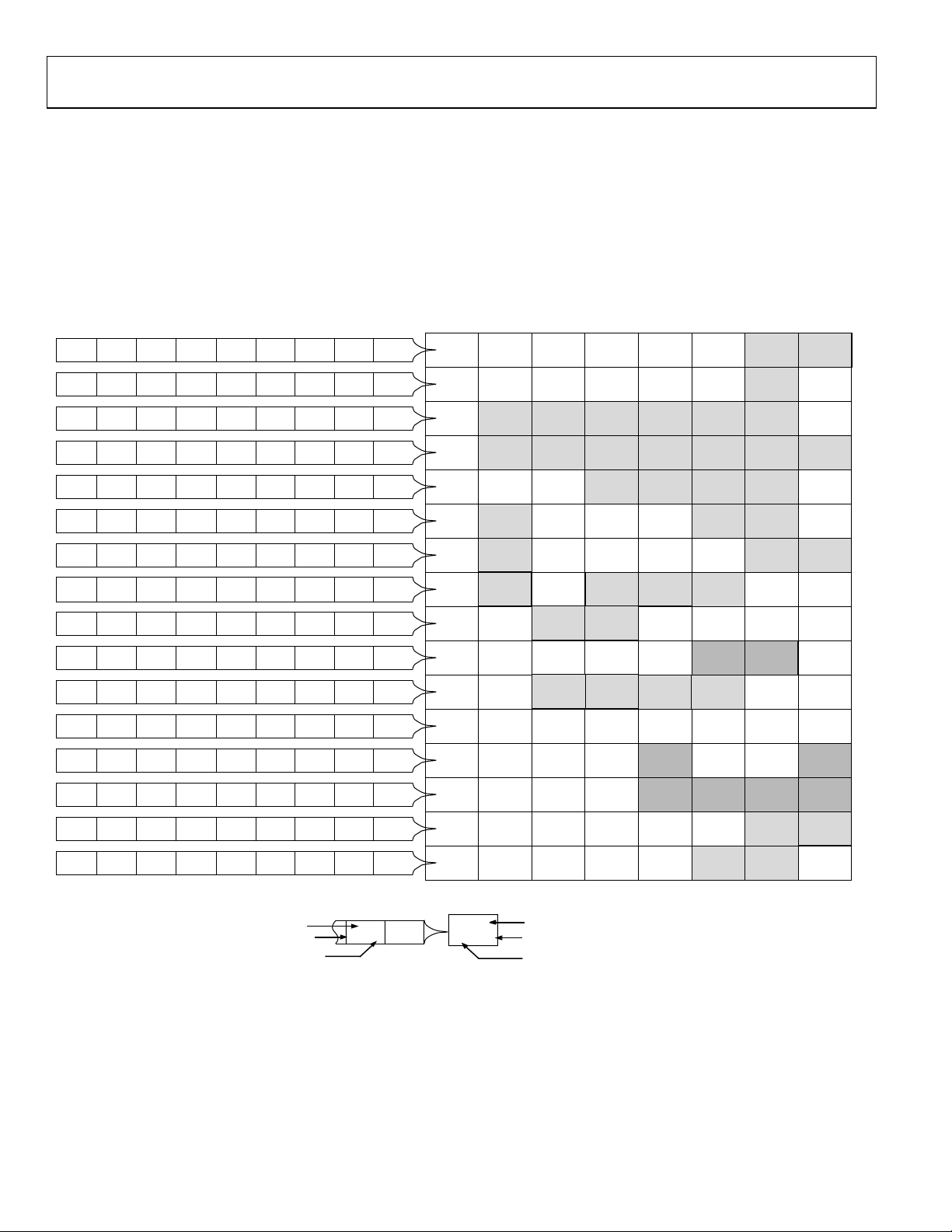
Rev. 0 | Page 22 of 88
03260-0-025
ADuC841/ADuC842/ADuC843
ADC CIRCUIT INFORMATION
General Overview
The ADC conversion block incorporates a fast, 8-channel,
12-bit, single-supply ADC. This block provides the user with
multichannel mux, track-and-hold, on-chip reference, calibration features, and ADC. All components in this block are easily
configured via a 3-register SFR interface.
The ADC converter consists of a conventional successive
approximation converter based around a capacitor DAC. The
converter accepts an analog input range of 0 V to V
. A high
REF
precision, 15 ppm, low drift, factory calibrated 2.5 V reference is
provided on-chip. An external reference can be connected as
described in the Voltage Reference Connections section. This
external reference can be in the range 1 V to AV
DD
.
Single-step or continuous conversion modes can be initiated in
software or alternatively by applying a convert signal to an
external pin. Timer 2 can also be configured to generate a
repetitive trigger for ADC conversions. The ADC may be
configured to operate in a DMA mode whereby the ADC block
continuously converts and captures samples to an external
RAM space without any interaction from the MCU core. This
automatic capture facility can extend through a 16 MByte
external data memory space.
The ADuC841/ADuC842/ADuC843 are shipped with factory
programmed calibration coefficients that are automatically
downloaded to the ADC on power-up, ensuring optimum ADC
performance. The ADC core contains internal offset and gain
calibration registers that can be hardware calibrated to
minimize system errors.
A voltage output from an on-chip band gap reference proportional to absolute temperature can also be routed through the
front end ADC multiplexer (effectively a 9th ADC channel
input), facilitating a temperature sensor implementation.
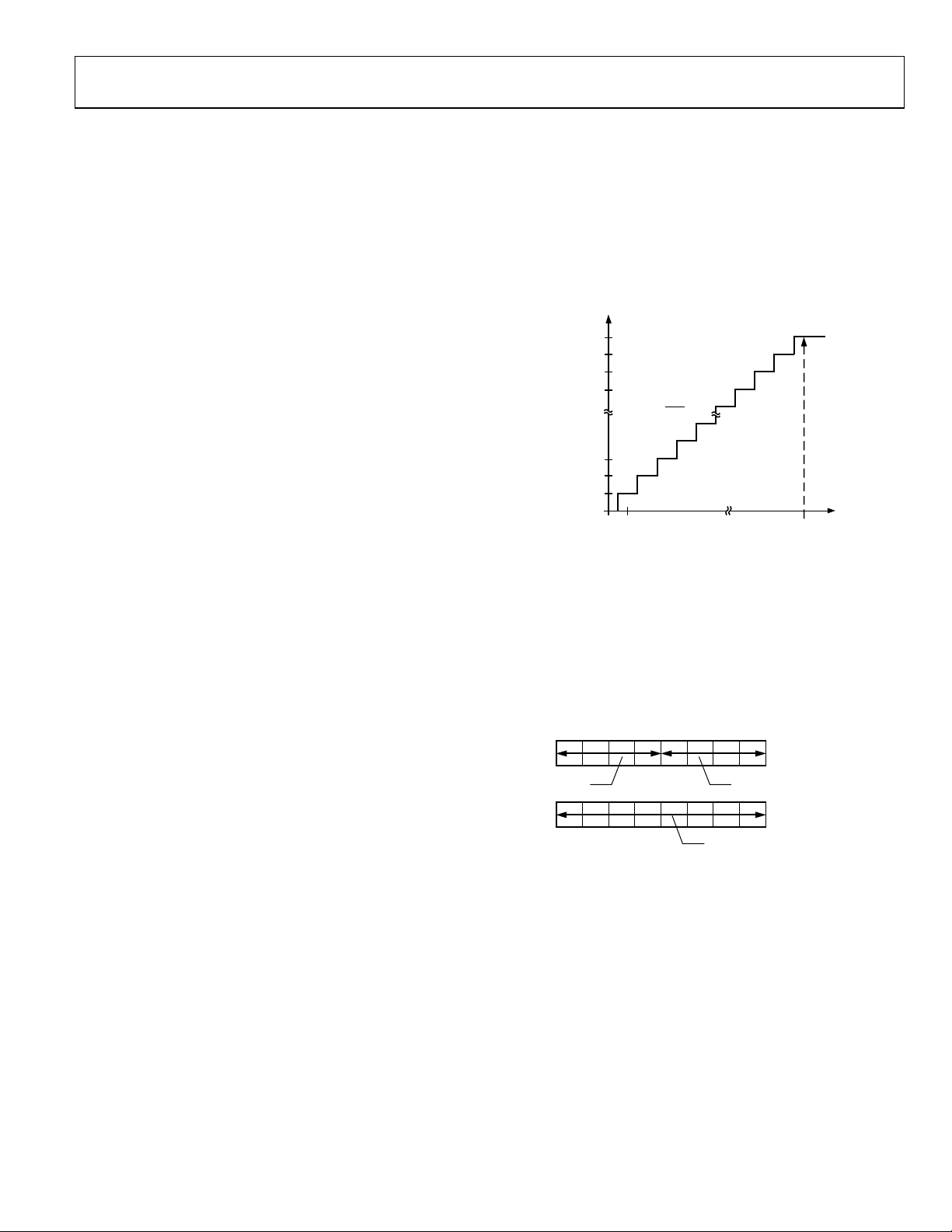
ADC Transfer Function
The analog input range for the ADC is 0 V to V
. For this
REF
range, the designed code transitions occur midway between
successive integer LSB values, i.e., 0.5 LSB, 1.5 LSB, 2.5 LSB . . .
FS –1.5 LSB. The output coding is straight binary with 1 LSB =
FS/4096 or 2.5 V/4096 = 0.61 mV when V
input/output transfer characteristic for the 0 V to V
= 2.5 V. The ideal
REF
range is
REF
shown in Figure 28.
OUTPUT
CODE
111...111
111...110
111...101
111...100
000...011
000...010
000...001
000...000
0V 1LSB
FS
1LSB =
4096
Figure 28. ADC Transfer Function
+FS
03260-0-026
Typical Operation
Once configured via the ADCCON 1–3 SFRs, the ADC converts
the analog input and provides an ADC 12-bit result word in the
ADCDATAH/L SFRs. The top 4 bits of the ADCDATAH SFR
are written with the channel selection bits to identify the channel
result. The format of the ADC 12-bit result word is shown in
Figure 29.
ADCDATAH SFR
CH–ID
TOP 4 BITS
Figure 29. ADC Result Word Format
HIGH 4 BITS OF
ADC RESULT WORD
LOW 8 BITS OF THE
ADC RESULT WORD
ADCDATAL SFR
03260-0-027
Rev. 0 | Page 23 of 88

ADuC841/ADuC842/ADuC843
ADCCON1—(ADC Control SFR 1)
The ADCCON1 register controls conversion and acquisition
times, hardware conversion modes, and power-down modes as
detailed below.
SFR Address EFH
SFR Power-On Default 40H
Bit Addressable No
Table 7. ADCCON1 SFR Bit Designations
Bit No. Name Description
7 MD1 The mode bit selects the active operating mode of the ADC.
Set by the user to power up the ADC.
Cleared by the user to power down the ADC.
6 EXT_REF Set by the user to select an external reference.
Cleared by the user to use the internal reference.
5
4
3
2
1 T2C
0 EXC
CK1
CK0
AQ1
AQ0
The ADC clock divide bits (CK1, CK0) select the divide ratio for the PLL master clock (ADuC842/ADuC843) or the
external crystal (ADuC841) used to generate the ADC clock. To ensure correct ADC operation, the divider ratio
must be chosen to reduce the ADC clock to 8.38 MHz or lower. A typical ADC conversion requires 16 ADC clocks
plus the selected acquisition time.
The divider ratio is selected as follows:
CK1
0
0
1
1
The ADC acquisition select bits (AQ1, AQ0) select the time provided for the input track-and-hold amplifier to
acquire the input signal. An acquisition of three or more ADC clocks is recommended; clocks are as follows:
AQ1
0
0
1
1
The Timer 2 conversion bit (T2C) is set by the user to enable the Timer 2 overflow bit to be used as the ADC
conversion start trigger input.
The external trigger enable bit (EXC) is set by the user to allow the external Pin P3.5 (
active low convert start input. This input should be an active low pulse (minimum pulse width >100 ns) at the
required sample rate.
CK0
0
1
0
1
AQ0
0
1
0
1
MCLK Divider
32
4 (Do not use with a CD setting of 0)
8
2
No. ADC Clks
1
2
3
4
CONVST
) to be used as the
Rev. 0 | Page 24 of 88

ADuC841/ADuC842/ADuC843
ADCCON2—(ADC Control SFR 2)
The ADCCON2 register controls ADC channel selection and
conversion modes as detailed below.
SFR Address D8H
SFR Power-On Default 00H
Bit Addressable Yes
Table 8. ADCCON2 SFR Bit Designations
Bit No. Name Description
7 ADCI ADC Interrupt Bit.
Set by hardware at the end of a single ADC conversion cycle or at the end of a DMA block conversion.
Cleared by hardware when the PC vectors to the ADC interrupt service routine. Otherwise, the ADCI bit is cleared
by user code.
6 DMA DMA Mode Enable Bit.
Set by the user to enable a preconfigured ADC DMA mode operation. A more detailed description of this mode is
given in the ADC DMA Mode section. The DMA bit is automatically set to 0 at the end of a DMA cycle. Setting this
bit causes the ALE output to cease; it will start again when DMA is started and will operate correctly after DMA is
complete.
5 CCONV Continuous Conversion Bit.
Set by the user to initiate the ADC into a continuous mode of conversion. In this mode, the ADC starts converting
based on the timing and channel configuration already set up in the ADCCON SFRs; the ADC automatically starts
another conversion once a previous conversion has completed.
4 SCONV Single Conversion Bit.
Set to initiate a single conversion cycle. The SCONV bit is automatically reset to 0 on completion of the single
conversion cycle.
3
2
1
0
CS3
CS2
CS1
CS0
Channel Selection Bits.
Allow the user to program the ADC channel selection under software control. When a conversion is initiated, the
converted channel is the one pointed to by these channel selection bits. In DMA mode, the channel selection is
derived from the channel ID written to the external memory.
CS3
0
0
0
0
0
0
0
0
1
1
1
1
1
1
All other combinations reserved.
CS2
0
0
0
0
1
1
1
1
0
0
0
0
1
1
CS1
0
0
1
1
0
0
1
1
0
0
1
1
0
1
CS0
0
1
0
1
0
1
0
1
0
1
0
1
0
1
CH#
0
1
2
3
4
5
6
7
Temp Monitor
DAC0
DAC1
AGND
V
REF
DMA STOP
Requires minimum of 1 µs to acquire.
Only use with internal DAC output buffer on.
Only use with internal DAC output buffer on.
Place in XRAM location to finish DMA sequence; refer to
the ADC DMA Mode section.
Rev. 0 | Page 25 of 88

ADuC841/ADuC842/ADuC843
ADCCON3—(ADC Control SFR 3)
The ADCCON3 register controls the operation of various
calibration modes and also indicates the ADC busy status.
SFR Address F5H
SFR Power-On Default 00H
Bit Addressable No
Table 9. ADCCON3 SFR Bit Designations
Bit No. Name Description
7 BUSY ADC Busy Status Bit.
A read-only status bit that is set during a valid ADC conversion or during a calibration cycle.
Busy is automatically cleared by the core at the end of conversion or calibration.
6 RSVD Reserved. This bit should always be written as 0.
5 AVGS1 Number of Average Selection Bits.
This bit selects the number of ADC readings that are averaged during a calibration cycle. 4 AVGS0
AVGS1
0
0
1
1
3 RSVD Reserved. This bit should always be written as 0.
2 RSVD This bit should always be written as 1 by the user when performing calibration.
1 TYPICAL Calibration Type Select Bit.
This bit selects between offset (zero-scale) and gain (full-scale) calibration.
Set to 0 for offset calibration.
Set to 1 for gain calibration.
0 SCAL Start Calibration Cycle Bit.
When set, this bit starts the selected calibration cycle.
It is automatically cleared when the calibration cycle is completed.
AVGS0
0
1
0
1
Number of Averages
15
1
31
63
Rev. 0 | Page 26 of 88
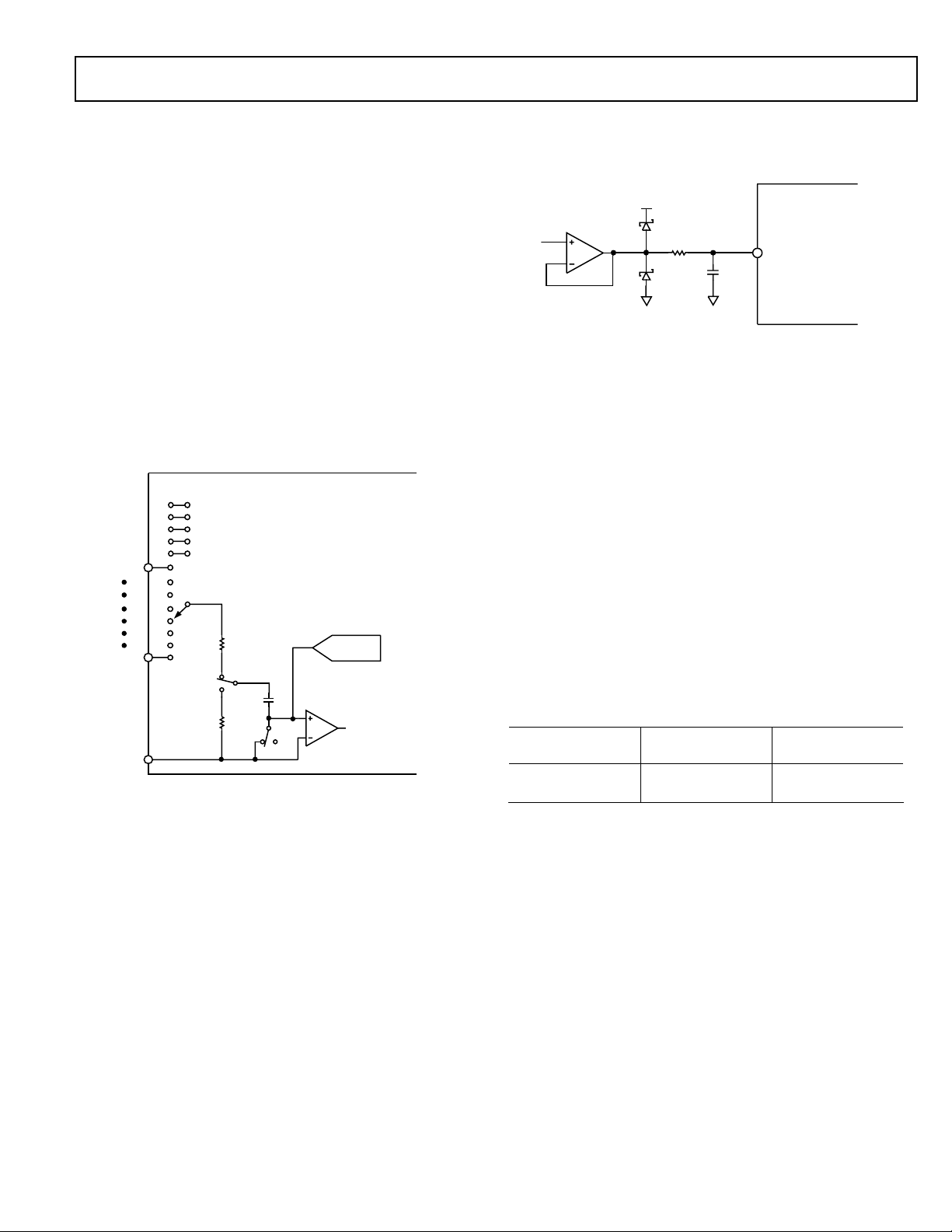
ADuC841/ADuC842/ADuC843
The ADC incorporates a successive approximation architecture
(SAR) involving a charge-sampled input stage. Figure 30 shows
the equivalent circuit of the analog input section. Each ADC
conversion is divided into two distinct phases, as defined by the
position of the switches in Figure 30. During the sampling
phase (with SW1 and SW2 in the track position), a charge
proportional to the voltage on the analog input is developed
across the input sampling capacitor. During the conversion
phase (with both switches in the hold position), the capacitor
DAC is adjusted via internal SAR logic until the voltage on
Node A is 0, indicating that the sampled charge on the input
capacitor is balanced out by the charge being output by the
capacitor DAC. The final digital value contained in the SAR is
then latched out as the result of the ADC conversion. Control of
the SAR and timing of acquisition and sampling modes is
handled automatically by built-in ADC control logic.
Acquisition and conversion times are also fully configurable
under user control.
ADuC841/ADuC842/ADuC843
V
REF
AGND
DAC1
DAC0
AIN7
AIN0
AGND
TEMPERATURE MONITOR
200Ω
sw1
TRACK
HOLD
32pF
NODE A
200Ω
TRACK
Figure 30. Internal ADC Structure
sw2
HOLD
CAPACITOR
COMPARATOR
DAC
03260-0-028
Note that whenever a new input channel is selected, a residual
charge from the 32 pF sampling capacitor places a transient on
the newly selected input. The signal source must be capable of
recovering from this transient before the sampling switches go
into hold mode. Delays can be inserted in software (between
channel selection and conversion request) to account for input
stage settling, but a hardware solution alleviates this burden
from the software design task and ultimately results in a cleaner
system implementation. One hardware solution is to choose a
very fast settling op amp to drive each analog input. Such an op
amp would need to fully settle from a small signal transient in
less than 300 ns in order to guarantee adequate settling under
all software configurations. A better solution, recommended for
use with any amplifier, is shown in Figure 31. Though at first
glance the circuit in Figure 31 may look like a simple antialiasing filter, it actually serves no such purpose since its corner
frequency is well above the Nyquist frequency, even at a 200
kHz sample rate. Though the R/C does help to reject some
incoming high frequency noise, its primary function is to ensure
that the transient demands of the ADC input stage are met.
ADuC841/
ADuC842/
10Ω
0.1µF
Figure 31. Buffering Analog Inputs
ADuC843
AIN0
03260-0-029
It does so by providing a capacitive bank from which the 32 pF
sampling capacitor can draw its charge. Its voltage does not
change by more than one count (1/4096) of the 12-bit transfer
function when the 32 pF charge from a previous channel is
dumped onto it. A larger capacitor can be used if desired, but
not a larger resistor (for reasons described below). The Schottky
diodes in Figure 31 may be necessary to limit the voltage
applied to the analog input pin per the Absolute Maximum
Ratings. They are not necessary if the op amp is powered from
the same supply as the part since in that case the op amp is
unable to generate voltages above V
or below ground. An op
DD
amp of some kind is necessary unless the signal source is very
low impedance to begin with. DC leakage currents at the parts’
analog inputs can cause measurable dc errors with external
source impedances as low as 100 Ω or so. To ensure accurate
ADC operation, keep the total source impedance at each analog
input less than 61 Ω. The Table 10 illustrates examples of how
source impedance can affect dc accuracy.
Table 10. Source Impedance and DC Accuracy
Source
Impedance Ω
Error from 1 µA
Leakage Current
Error from 10 µA
Leakage Current
61 61 µV = 0.1 LSB 610 µV = 1 LSB
610 610 µV = 1 LSB 6.1 mV = 10 LSB
Although Figure 31 shows the op amp operating at a gain of 1,
one can, of course, configure it for any gain needed. Also, one
can just as easily use an instrumentation amplifier in its place to
condition differential signals. Use an amplifier that is capable of
delivering the signal (0 V to V
) with minimal saturation.
REF
Some single-supply rail-to-rail op amps that are useful for this
purpose are described in Table 11. Check Analog Devices website
www.analog.com for details on these and other op amps and
instrumentation amps.
Rev. 0 | Page 27 of 88
 Loading...