MicroConverter®, Dual-Channel
a
16-/24-Bit ADCs with Embedded FLASH MCU
FEATURES
High Resolution Sigma-Delta ADCs
Two Independent ADCs (16- and 24-Bit Resolution)
Programmable Gain Front End
24-Bit No Missing Codes, Primary ADC
13-Bit p-p Resolution @ 20 Hz, 20 mV Range
18-Bit p-p Resolution @ 20 Hz, 2.56 V Range
Memory
8 KB On-Chip Flash/EE Program Memory
640 Bytes On-Chip Flash/EE Data Memory
Flash/EE, 100 Year Retention, 100 Kcycles Endurance
256 Bytes On-Chip Data RAM
8051-Based Core
8051-Compatible Instruction Set (12.58 MHz Max)
32 kHz External Crystal, On-Chip Programmable PLL
Three 16-Bit Timer/Counters
26 Programmable I/O Lines
11 Interrupt Sources, Two Priority Levels
Power
Specified for 3 V and 5 V Operation
Normal: 3 mA @ 3 V (Core CLK = 1.5 MHz)
Power-Down: 20 A (32 kHz Crystal Running)
On-Chip Peripherals
On-Chip Temperature Sensor
12-Bit Voltage Output DAC
Dual Excitation Current Sources
Reference Detect Circuit
Time Interval Counter (TIC)
UART Serial I/O
2C®
-Compatible and SPI® Serial I/O
I
Watchdog Timer (WDT), Power Supply Monitor (PSM)
APPLICATIONS
Intelligent Sensors (IEEE1451.2-Compatible)
Weigh Scales
Portable Instrumentation
Pressure Transducers
4–20 mA Transmitters
GENERAL DESCRIPTION
The ADuC824 is a complete smart transducer front-end, integrating two high-resolution sigma delta ADCs, an 8-bit MCU,
and program/data Flash/EE Memory on a single chip. This low
power device accepts low-level signals directly from a transducer.
The two independent ADCs (Primary and Auxiliary) include a
temperature sensor and a PGA (allowing direct measurement of
MicroConverter is a registered trademark of Analog Devices, Inc.
SPI is a registered trademark of Motorola, Inc.
I2C is a registered trademark of Philips Semiconductors, Inc.
REV.B
Information furnished by Analog Devices is believed to be accurate and
reliable. However, no responsibility is assumed by Analog Devices for its
use, nor for any infringements of patents or other rights of third parties that
may result from its use. No license is granted by implication or otherwise
under any patent or patent rights of Analog Devices.
ADuC824
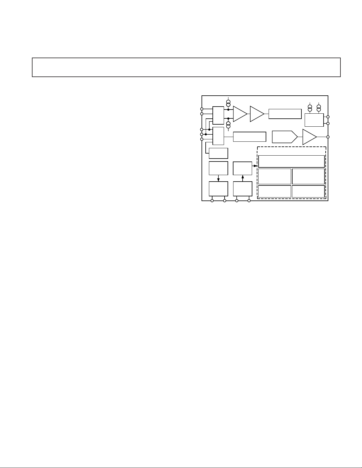
FUNCTIONAL BLOCK DIAGRAM
AIN1
AIN2
AIN3
AIN4
AIN5
AVDD
MUX
MUX
TEMP
SENSOR
INTERNAL
BANDGAP
VREF
EXTERNAL
VREF
DETECT
REFIN+REFIN–
BUF
AGND
CLOCK
DIVIDER
PGA
AUXILIARY
16-BIT - ADC
PROG.
OSC
AND
PLL
XTAL2XTAL1
ADuC824
PRIMARY
24-BIT - ADC
12-BIT
VOLTAGE O/P
DAC
8051-BASED MCU WITH ADDITIONAL
8 KBYTES FLASH/EE PROGRAM MEMORY
TIMER/COUNTERS
1 TIME INTERVAL
PERIPHERALS
640 BYTES FLASH/EE DATA MEMORY
256 BYTES USER RAM
3 16 BIT
COUNTER
4 PARALLEL
PORTS
low-level signals). The ADCs with on-chip digital filtering are
intended for the measurement of wide dynamic range, low-frequency
signals, such as those in weigh scale, strain-gauge, pressure transducer, or temperature measurement applications. The ADC output
data rates are programmable and the ADC output resolution will
vary with the programmed gain and output rate.
The device operates from a 32 kHz crystal with an on-chip PLL
generating a high-frequency clock of 12.58 MHz. This clock is,
in turn, routed through a programmable clock divider from
which the MCU core clock operating frequency is generated. The
microcontroller core is an 8052 and therefore 8051-instructionset-compatible. The microcontroller core machine cycle consists
of 12 core clock periods of the selected core operating frequency.
8 Kbytes of nonvolatile Flash/EE program memory are provided
on-chip. 640 bytes of nonvolatile Flash/EE data memory and
256 bytes RAM are also integrated on-chip.
The ADuC824 also incorporates additional analog functionality
with a 12-bit DAC, current sources, power supply monitor,
and a bandgap reference. On-chip digital peripherals include a
watchdog timer, time interval counter, three timers/counters,
and three serial I/O ports (SPI, UART, and I
On-chip factory firmware supports in-circuit serial download and
debug modes (via UART), as well as single-pin emulation mode
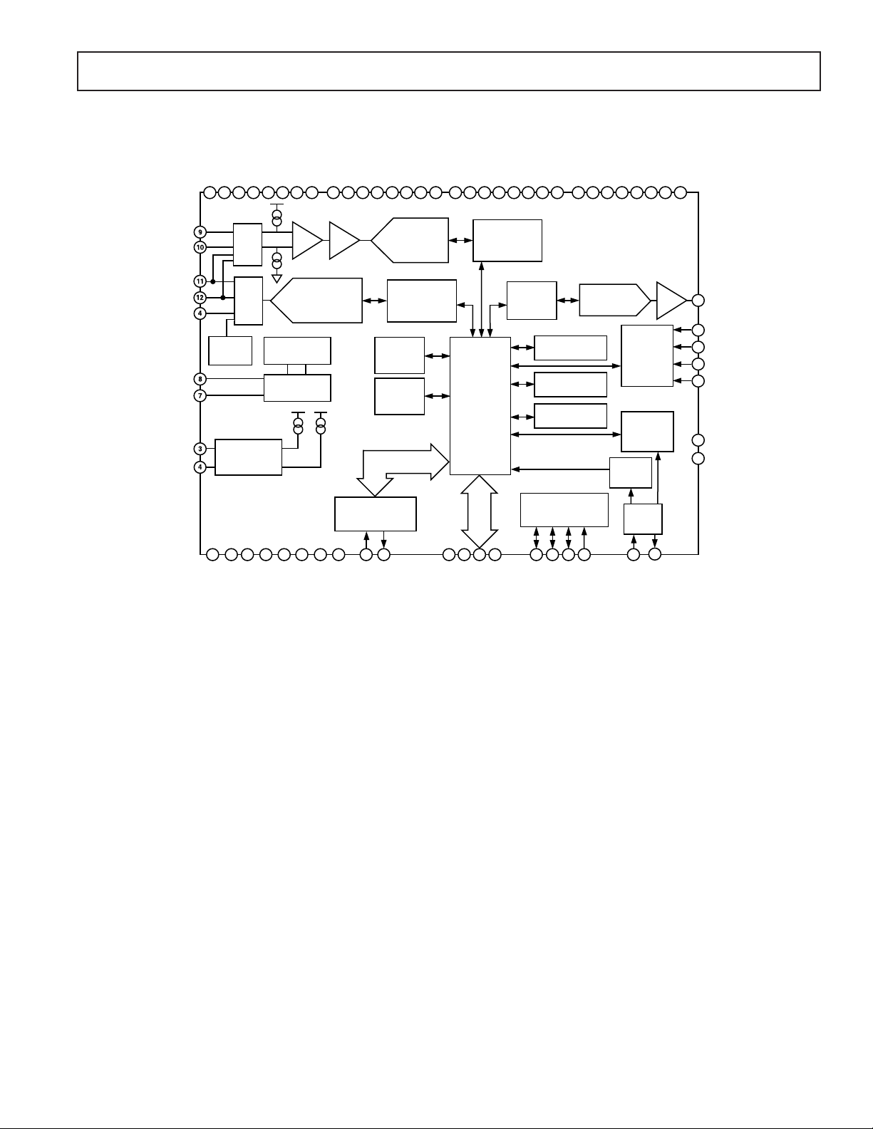
via the EA pin. A functional block diagram of the ADuC824 is
shown above with a more detailed block diagram shown in
Figure 12.
The part operates from a single 3 V or 5 V supply. When operating
from 3 V supplies, the power dissipation for the part is below
10 mW. The ADuC824 is housed in a 52-lead MQFP package.
One Technology Way, P.O. Box 9106, Norwood, MA 02062-9106, U.S.A.
Tel: 781/329-4700 www.analog.com
Fax: 781/326-8703 © Analog Devices, Inc., 2002
AVDD
CURRENT
SOURCE
MUX
BUF
ON-CHIP MONITORS
POWER SUPPLY
MONITOR
WATCHDOG TIMER
I2C-COMPATIBLE
UART AND SPI
SERIAL I/O
2
C-compatible).
IEXC1
IEXC2
DAC

ADuC824
TABLE OF CONTENTS
FEATURES .......................................................................... 1
GENERAL DESCRIPTION ................................................. 1
SPECIFICATIONS .............................................................. 3
TIMING SPECIFICATIONS .............................................. 8
ABSOLUTE MAXIMUM RATINGS................................. 18
PIN CONFIGURATION .................................................... 18
ORDERING GUIDE .......................................................... 18
PIN FUNCTION DESCRIPTIONS................................... 19
ADuC824 BLOCK DIAGRAM .......................................... 21
MEMORY ORGANIZATION ............................................ 22
OVERVIEW OF MCU-RELATED SFRS ........................... 23
Accumulator (ACC) ........................................................ 23
B SFR (B) ....................................................................... 23
Stack Pointer (SP) ........................................................... 23
Data Pointer (DPTR) ...................................................... 23
Program Status Word (PSW) ........................................... 23
Power Control (PCON) ................................................... 23
SPECIAL FUNCTION REGISTERS ................................. 24
SFR INTERFACE TO THE PRIMARY AND
AUXILIARY ADCs ......................................................... 25
ADCSTAT ...................................................................... 25
ADCMODE .................................................................... 26
ADC0CON ..................................................................... 27
ADC1CON ..................................................................... 28
SF ................................................................................... 28
ICON .............................................................................. 29
ADC0H/ADC0M/ADC0L ............................................... 29
ADC1H/ADC1L ............................................................. 29
OF0H/OF0M/OF0L ........................................................ 30
OF1H/OF1L ................................................................... 30
GN0H/GN0M/GN0L ...................................................... 30
GN1H/GN1L .................................................................. 30
PRIMARY AND AUXILIARY ADC DESCRIPTION........ 31
Overview ......................................................................... 31
Primary ADC .................................................................. 31
Auxiliary ADC ................................................................. 32
PRIMARY AND AUXILIARY ADC NOISE
PERFORMANCE ............................................................ 33
Analog Input Channels .................................................... 33
Primary and Auxiliary ADC Inputs .................................. 33
Analog Input Ranges ........................................................ 33
Programmable Gain Amplifier .......................................... 34
Bipolar/Unipolar Inputs ................................................... 34
Burnout Currents............................................................. 34
Excitation Currents .......................................................... 35
Reference Input ............................................................... 35
Reference Detect ............................................................. 35
Sigma-Delta Modulator ................................................... 35
Digital Filter .................................................................... 35
ADC Chopping ............................................................... 36
Calibration ...................................................................... 37
NONVOLATILE FLASH/EE MEMORY ........................... 37
Flash/EE Memory Overview ............................................. 37
Flash/EE Memory and the ADuC824 ............................... 37
ADuC824 Flash/EE Memory Reliability ........................... 37
Using the Flash/EE Program Memory .............................. 38
Flash/EE Program Memory Security ................................ 39
Using the Flash/EE Data Memory .................................... 39
USER INTERFACE TO OTHER ON-CHIP ADuC824
PERIPHERALS .............................................................. 41
DAC ................................................................................ 41
On-Chip PLL .................................................................. 42
Time Interval Counter (TIC) ........................................... 43
Watchdog Timer .............................................................. 46
Power Supply Monitor ..................................................... 47
Serial Peripheral Interface ................................................ 48
2
C-Compatible Interface ................................................. 50
I
8051-COMPATIBLE ON-CHIP PERIPHERALS .............. 51
Parallel I/O Ports 0–3 ....................................................... 51
Timers/Counters .............................................................. 51
TIMER/COUNTER 0 AND 1 OPERATING MODES ...... 54
UART Serial Interface ..................................................... 57
Interrupt System .............................................................. 60
ADuC824 HARDWARE DESIGN CONSIDERATIONS... 62
Clock Oscillator ............................................................... 62
External Memory Interface............................................... 62
Power-On Reset Operation .............................................. 63
Power Supplies ................................................................ 63
Power Consumption ........................................................ 64
Power-Saving Modes ....................................................... 64
Grounding and Board Layout Recommendations ............. 64
ADuC824 System Self-Identification................................ 65
OTHER HARDWARE CONSIDERATIONS..................... 65
In-Circuit Serial Download Access ................................... 65
Embedded Serial Port Debugger ...................................... 65
Single-Pin Emulation Mode ............................................. 65
Enhanced-Hooks Emulation Mode .................................. 66
Typical System Configuration .......................................... 66
QUICKSTART DEVELOPMENT SYSTEM..................... 67
OUTLINE DIMENSIONS ................................................. 68
Revision History .................................................................. 68
–2–
REV. B

ADuC824
(AVDD = 2.7 V to 3.6 V or 4.75 V to 5.25 V, DVDD = 2.7 V to 3.6 V or 4.75 V to 5.25 V, REFIN(+) = 2.5 V;
1
SPECIFICATIONS
unless otherwise noted.)
Parameter ADuC824BS Test Conditions/Comments Unit
ADC SPECIFICATIONS
Conversion Rate 5.4 On Both Channels Hz min
Primary ADC
No Missing Codes
Resolution 13 Range = ± 20 mV, 20 Hz Update Rate Bits p-p typ
Output Noise See Tables IX and X Output Noise Varies with Selected
Integral Nonlinearity ± 15 ppm of FSR max
Offset Error
Offset Error Drift ± 10 nV/°C typ
Full-Scale Error
Gain Error Drift
ADC Range Matching ±2 AIN = 18 mV µV typ
Power Supply Rejection (PSR) 113 AIN = 7.8 mV, Range = ± 20 mV dBs typ
Common-Mode DC Rejection
On AIN 95 At DC, AIN = 7.8 mV, Range = ±20 mV dBs min
On AIN 113 At DC, AIN = 1 V, Range = ± 2.56 V dBs typ
On REFIN 125 At DC, AIN = 1 V, Range = ±2.56 V dBs typ
Common-Mode 50 Hz/60Hz Rejection
On AIN 95 50 Hz/60 Hz ±1 Hz, AIN = 7.8 mV, dBs min
On REFIN 90 50 Hz/60 Hz ±1 Hz, AIN = 1 V, dBs min
Normal Mode 50 Hz/60 Hz Rejection
On AIN 60 50 Hz/60 Hz ±1 Hz, 20 Hz Update Rate dBs min
On REFIN 60 50 Hz/60 Hz ±1 Hz, 20 Hz Update Rate dBs min
Auxiliary ADC
No Missing Codes
Resolution 16 Range = ± 2.5 V, 20 Hz Update Rate Bits p-p typ
Output Noise See Table XI Output Noise Varies with Selected
Integral Nonlinearity ± 15 ppm of FSR max
Offset Error
Offset Error Drift 1 µV/°C typ
Full-Scale Error
Gain Error Drift
Power Supply Rejection (PSR) 80 AIN = 1 V, 20 Hz Update Rate dBs min
Normal Mode 50 Hz/60 Hz Rejection
On AIN 60 50 Hz/60 Hz ±1 Hz dBs min
On REFIN 60 50 Hz/60 Hz ±1 Hz, 20 Hz Update Rate dBs min
DAC PERFORMANCE
DC Specifications
Resolution 12 Bits
Relative Accuracy ± 3 LSB typ
Differential Nonlinearity –1 Guaranteed 12-Bit Monotonic LSB max
Offset Error ± 50 mV max
Gain Error
AC Specifications
Voltage Output Settling Time 15 Settling Time to 1 LSB of Final Value µs typ
Digital-to-Analog Glitch Energy 10 1 LSB Change at Major Carry nVs typ
2
3
4
5
2
3
6
5
7
8
2, 7
REFIN(–) = AGND; AGND = DGND = 0 V; XTAL1/XTAL2 = 32.768 kHz Crystal; all specifications T
105 Programmable in 0.732 ms Increments Hz max
24 20 Hz Update Rate Bits min
18 Range = ±2.56 V, 20 Hz Update Rate Bits p-p typ
in ADC Description Update Rate and Gain Range
± 3 µV typ
± 10 µV typ
± 0.5 ppm/°C typ
80 AIN = 1 V, Range = ±2.56 V dBs min
2
20 Hz Update Rate
Range = ± 20 mV
90 50 Hz/60 Hz ±1 Hz, AIN = 1 V, dBs min
Range = ±2.56 V
2
Range = ±2.56 V
16 Bits min
in ADC Description Update Rate
–2 LSB typ
–2.5 LSB typ
± 0.5 ppm/°C typ
2
± 1AV
± 1V
Range % max
DD
Range % typ
REF
MIN
to T
MAX
REV. B
–3–

ADuC824
Parameter ADuC824BS Test Conditions/Comments Unit
INTERNAL REFERENCE
ADC Reference
Reference Voltage 1.25 ± 1% Initial Tolerance @ 25°C, V
Power Supply Rejection 45 dBs typ
Reference Tempco 100 ppm/°C typ
DAC Reference
Reference Voltage 2.5 ± 1% Initial Tolerance @ 25°C, VDD = 5 V V min/max
Power Supply Rejection 50 dBs typ
Reference Tempco ± 100 ppm/°C typ
ANALOG INPUTS/REFERENCE INPUTS
Primary ADC
Differential Input Voltage Ranges
9, 10
External Reference Voltage = 2.5 V
RN2, RN1, RN0 of ADC0CON Set to
Bipolar Mode (ADC0CON3 = 0) ±20 0 0 0 (Unipolar Mode 0 to 20 mV) mV
± 40 0 0 1 (Unipolar Mode 0 to 40 mV) mV
± 80 0 1 0 (Unipolar Mode 0 to 80 mV) mV
± 160 0 1 1 (Unipolar Mode 0 to 160 mV) mV
± 320 1 0 0 (Unipolar Mode 0 to 320 mV) mV
± 640 1 0 1 (Unipolar Mode 0 to 640 mV) mV
± 1.28 1 1 0 (Unipolar Mode 0 to 1.28 V) V
± 2.56 1 1 1 (Unipolar Mode 0 to 2.56 V) V
± 1 nA max
Analog Input Current
2
Analog Input Current Drift ± 5pA/°C typ
Absolute AIN Voltage Limits AGND + 100 mV V min
– 100 mV V max
AV
Auxiliary ADC
Input Voltage Range
9, 10
DD
0 to V
REF
Unipolar Mode, for Bipolar Mode V
See Note 11
Average Analog Input Current 125 Input Current Will Vary with Input nA/V typ
Average Analog Input Current Drift
Absolute AIN Voltage Limits
External Reference Inputs
REFIN(+) to REFIN(–) Range
2
11
2
± 2 Voltage on the Unbuffered Auxiliary ADC pA/V/°C typ
AGND – 30 mV V min
+ 30 mV V max
AV
DD
1V min
AV
DD
Average Reference Input Current 1 Both ADCs Enabled µA/V typ
Average Reference Input Current Drift ± 0.1 nA/V/°C typ
‘NO Ext. REF’ Trigger Voltage 0.3 NOXREF Bit Active if V
0.65 NOXREF Bit Inactive if V
ADC SYSTEM CALIBRATION
Full-Scale Calibration Limit +1.05 × FS V max
Zero-Scale Calibration Limit –1.05 × FS V min
Input Span +0.8 × FS V min
+2.1 × FS V max
ANALOG (DAC) OUTPUTS
Voltage Range 0 to V
0 to AV
REF
DD
DACRN = 0 in DACCON SFR V typ
DACRN = 1 in DACCON SFR V typ
Resistive Load 10 From DAC Output to AGND kΩ typ
Capacitive Load 100 From DAC Output to AGND pF typ
Output Impedance 0.5 Ω typ
I
SINK
50 µA typ
TEMPERATURE SENSOR
Accuracy ± 2 °C typ
Thermal Impedance (θJA)90 °C/W typ
= 5 V V min/max
DD
< 0.3 V V min
REF
> 0.65 V V max
REF
V max
–4–
REV. B

Parameter ADuC824BS Test Conditions/Comments Unit
TRANSDUCER BURNOUT CURRENT SOURCES
AIN+ Current –100 AIN+ is the Selected Positive Input to nA typ
the Primary ADC
AIN– Current +100 AIN– is the Selected Negative Input to nA typ
the Auxiliary ADC
Initial Tolerance @ 25°C Drift ±10 % typ
Drift 0.03 %/°C typ
EXCITATION CURRENT SOURCES
Output Current –200 Available from Each Current Source µA typ
Initial Tolerance @ 25°C ± 10 % typ
Drift 200 ppm/°C typ
Initial Current Matching @ 25°C ± 1 Matching Between Both Current Sources % typ
Drift Matching 20 ppm/°C typ
Line Regulation (AV
)1 AV
DD
= 5 V + 5% µA/V typ
DD
Load Regulation 0.1 µA/V typ
Output Compliance AV
– 0.6 V max
DD
AGND min
LOGIC INPUTS
All Inputs Except SCLOCK, RESET,
and XTAL1
, Input Low Voltage 0.8 DVDD = 5 V V max
V
INL
V
, Input High Voltage 2.0 V min
INH
SCLOCK and RESET Only
(Schmitt-Triggered Inputs)
V
T+
V
T–
– V
V
T+
T–
2
0.4 DV
= 3 V V max
DD
1.3/3 DVDD = 5 V V min/V max
0.95/2.5 DV
= 3 V V min/V max
DD
0.8/1.4 DVDD = 5 V V min/V max
0.4/1.1 DV
= 3 V V min/V max
DD
0.3/0.85 DVDD = 5 V V min/V max
0.3/0.85 DV
= 3 V V min/V max
DD
Input Currents
Port 0, P1.2–P1.7, EA ± 10 V
SCLOCK, SDATA/MOSI, MISO, SS
12
–10 min, –40 max VIN = 0 V, DVDD = 5 V, Internal Pull-Up µA min/µA max
± 10 V
RESET ± 10 V
35 min, 105 max V
= 0 V or V
IN
= VDD, DVDD = 5 V µA max
IN
= 0 V, DVDD = 5 V µA max
IN
= VDD, DVDD = 5 V, µA min/µA max
IN
DD
µA max
Internal Pull-Down
P1.0, P1.1, Ports 2 and 3 ± 10 V
–180 V
= VDD, DVDD = 5 V µA max
IN
= 2 V, DVDD = 5 V µA min
IN
–660 µA max
–20 V
= 450 mV, DVDD = 5 V µA min
IN
–75 µA max
Input Capacitance 5 All Digital Inputs pF typ
CRYSTAL OSCILLATOR (XTAL1 AND XTAL2)
Logic Inputs, XTAL1 Only
, Input Low Voltage 0.8 DVDD = 5 V V max
V
INL
V
, Input High Voltage 3.5 DVDD = 5 V V min
INH
0.4 DV
2.5 DV
= 3 V V max
DD
= 3 V V min
DD
XTAL1 Input Capacitance 18 pF typ
XTAL2 Output Capacitance 18 pF typ
ADuC824
REV. B
–5–

ADuC824
Parameter ADuC824BS Test Conditions/Comments Unit
LOGIC OUTPUTS (Not Including XTAL2)
VOH, Output High Voltage 2.4 VDD = 5 V, I
, Output Low Voltage
V
OL
13
Floating State Leakage Current ± 10 µA max
Floating State Output Capacitance 5 pF typ
POWER SUPPLY MONITOR (PSM)
Trip Point Selection Range 2.63 Four Trip Points Selectable in This Range V min
AV
DD
Power Supply Trip Point Accuracy ± 3.5 % max
AV
DD
Trip Point Selection Range 2.63 Four Trip Points Selectable in This Range V min
DV
DD
DVDD Power Supply Trip Point Accuracy ±3.5 % max
WATCHDOG TIMER (WDT)
Timeout Period 0 Nine Timeout Periods in This Range ms min
MCU CORE CLOCK RATE Clock Rate Generated via On-Chip PLL
MCU Clock Rate
2
START-UP TIME
At Power-On 300 ms typ
From Idle Mode 1 ms typ
From Power-Down Mode
Oscillator Running OSC_PD Bit = 0 in PLLCON SFR
Wakeup with INT0 Interrupt 1 ms typ
Wakeup with SPI/I
2
C Interrupt 1 ms typ
Wakeup with TIC Interrupt 1 ms typ
Wakeup with External RESET 3.4 ms typ
Oscillator Powered Down OSC_PD Bit = 1 in PLLCON SFR
Wakeup with External RESET 0.9 sec typ
After External RESET in Normal Mode 3.3 ms typ
After WDT Reset in Normal Mode 3.3 Controlled via WDCON SFR ms typ
FLASH/EE MEMORY RELIABILITY CHARACTERISTICS
Endurance
Data Retention
15
16
POWER REQUIREMENTS DV
Power Supply Voltages
, 3 V Nominal Operation 2.7 V min
AV
DD
, 5 V Nominal Operation 4.75 V min
AV
DD
DV
, 3 V Nominal Operation 2.7 V min
DD
, 5 V Nominal Operation 4.75 V min
DV
DD
2
= 80 µAV min
2.4 V
0.4 I
0.4 I
0.4 I
DD
SINK
SINK
SINK
= 3 V, I
SOURCE
= 20 µAV min
SOURCE
= 8 mA, SCLOCK, SDATA/MOSI V max
= 10 mA, P1.0 and P1.1 V max
= 1.6 mA, All Other Outputs V max
4.63 Programmed via TPA1–0 in PSMCON V max
4.63 Programmed via TPD1–0 in PSMCON V max
2000 Programmed via PRE3–0 in WDCON ms max
98.3 Programmable via CD2–0 Bits in kHz min
PLLCON SFR
12.58 MHz max
14
100,000 Cycles min
100 Years min
and AVDD Can Be Set
DD
Independently
3.6 V max
5.25 V max
3.6 V max
5.25 V max
–6–
REV. B
D

ADuC824
Parameter ADuC824BS Test Conditions/Comments Unit
POWER REQUIREMENTS (continued)
Power Supply Currents Normal Mode
DVDD Current 4 DVDD = 4.75 V to 5.25 V, Core CLK = 1.57 MHz mA max
AV
Current 170 AVDD = 5.25 V, Core CLK = 1.57 MHz µA max
DD
Current 15 DVDD = 4.75 V to 5.25 V, Core CLK = 12.58 MHz mA max
DV
DD
AV
Current 170 AVDD = 5.25 V, Core CLK = 12.58 MHz µA max
DD
Power Supply Currents Idle Mode
DVDD Current 1.2 DVDD = 4.75 V to 5.25 V, Core CLK = 1.57 MHz mA max
Current 140 Measured @ AVDD = 5.25 V, Core CLK = 1.57 MHz µA typ
AV
DD
DV
Current 2 DVDD = 4.75 V to 5.25 V, Core CLK = 12.58 MHz mA typ
DD
Current 140 Measured at AVDD = 5.25 V, Core CLK = 12.58 MHz µA typ
AV
DD
Power Supply Currents Power-Down Mode
DV
Current 50 DVDD = 4.75 V to 5.25 V, Osc. On, TIC On µA max
DD
AV
Current 1 Measured at AVDD = 5.25 V, Osc. On or Osc. Off µA max
DD
DV
Current 20 DVDD = 4.75 V to 5.25 V, Osc. Off µA max
DD
Typical Additional Power Supply Currents Core CLK = 1.57 MHz, AV
(AI
and DIDD)
DD
PSM Peripheral 50 µA typ
Primary ADC 1 mA typ
Auxiliary ADC 500 µA typ
DAC 150 µA typ
Dual Current Sources 400 µA typ
NOTES
1
Temperature Range: –40°C to +85°C.
2
These numbers are not production tested but are guaranteed by Design and/or Characterization data on production release.
3
System Zero-Scale Calibration can remove this error.
4
The primary ADC is factory calibrated at 25°C with AVDD = DVDD = 5 V yielding this full-scale error of 10 µV. If user power supply or temperature conditions are
significantly different than these, an Internal Full-Scale Calibration will restore this error to 10 µV. A system zero-scale and full-scale calibration will remove this
error altogether.
5
Gain Error Drift is a span drift. To calculate Full-Scale Error Drift, add the Offset Error Drift to the Gain Error Drift times the full-scale input.
6
The auxiliary ADC is factory calibrated at 25°C with AVDD = DVDD = 5 V yielding this full-scale error of –2.5 LSB. A system zero-scale and full-scale calibration
will remove this error altogether.
7
DAC linearity and AC Specifications are calculated using:
reduced code range of 48 to 4095, 0 to V
reduced code range of 48 to 3995, 0 to VDD.
8
Gain Error is a measure of the span error of the DAC.
9
In general terms, the bipolar input voltage range to the primary ADC is given by Range
V
= REFIN(+) to REFIN(–) voltage and V
REF
and RN2, RN1, RN0 = 1, 1, 0 the Range
10
1.25 V is used as the reference voltage to the ADC when internal V
11
In bipolar mode, the Auxiliary ADC can only be driven to a minimum of A
range is still –V
12
Pins configured in I2C-compatible mode or SPI mode, pins configured as digital inputs during this test.
13
Pins configured in I2C-compatible mode only.
14
Flash/EE Memory Reliability Characteristics apply to both the Flash/EE program memory and Flash/EE data memory.
15
Endurance is qualified to 100 Kcycles as per JEDEC Std. 22 method A117 and measured at –40 °C, +25°C and +85°C; typical endurance at 25°C is 700 K cycles.
16
Retention lifetime equivalent at junction temperature (TJ) = 55°C as per JEDEC Std. 22, Method A117. Retention lifetime based on an activation energy of 0.6e V
will derate with junction temperature as shown in Figure 27 in the Flash/EE Memory description section of this data sheet.
17
Power Supply current consumption is measured in Normal, Idle, and Power-Down Modes under the following conditions:
Normal Mode: Reset = 0.4 V, Digital I/O pins = open circuit, Core Clk changed via CD bits in PLLCON, Core Executing internal software loop.
Idle Mode: Reset = 0.4 V, Digital I/O pins = open circuit, Core Clk changed via CD bits in PLLCON, PCON.0 = 1, Core Execution suspended in idle mode.
Power-Down Mode: Reset = 0.4 V, All P0 pins and P1.2–P1.7 pins = 0.4 V, All other digital I/O pins are open circuit, Core Clk changed via CD bits in
PLLCON, PCON.1 = 1, Core Execution suspended in power-down mode, OSC turned ON or OFF via OSC_PD bit (PLLCON.7) in PLLCON SFR.
18
DVDD power supply current will increase typically by 3 mA (3 V operation) and 10 mA (5 V operation) during a Flash/EE memory program or erase cycle.
Specifications subject to change without notice.
REF
to +V
; however, the negative voltage is limited to –30 mV.
REF
17, 18
2.1 DV
8DV
17, 18
750 DV
1DV
17, 18
20 DV
5DV
,
REF
= 1.25 V when internal ADC V
REF
= ± 1.28 V. In unipolar mode the effective range is 0 V to 1.28 V in our example.
ADC
is selected via XREF0 and XREF1 bits in ADC0CON and ADC1CON, respectively.
REF
REF
– 30 mV as indicated by the Auxiliary ADC absolute AIN voltage limits. The bipolar
GND
= 2.7 V to 3.6 V, Core CLK = 1.57 MHz mA max
DD
= 2.7 V to 3.6 V, Core CLK = 12.58 MHz mA max
DD
= 2.7 V to 3.6 V, Core CLK = 1.57 MHz µA typ
DD
= 2.7 V to 3.6 V, Core CLK = 12.58 MHz mA typ
DD
Core CLK = 1.57 MHz or 12.58 MHz
= 2.7 V to 3.6 V, Osc. On, TIC On µA max
DD
= 2.7 V to 3.6 V, Osc. Off µA typ
DD
= ± (V
ADC
is selected. RN = decimal equivalent of RN2, RN1, RN0, e.g., V
2RN)/125, where:
REF
= DVDD = 5 V
DD
REF
= 2.5 V
REV. B
–7–
ADuC824
(AVDD = 2.7 V to 3.6 V or 4.75 V to 5.25 V, DVDD = 2.7 V to 3.6 V or 4.75 V to 5.25 V;
all specifications T
MIN
to T
unless otherwise noted.)
MAX
TIMING SPECIFICATIONS
1, 2, 3
32.768 kHz External Crystal
Parameter Min Typ Max Unit Figure
CLOCK INPUT (External Clock Driven XTAL1)
t
CK
t
CKL
t
CKH
t
CKR
t
CKF
1/t
CORE
t
CORE
t
CYC
NOTES
1
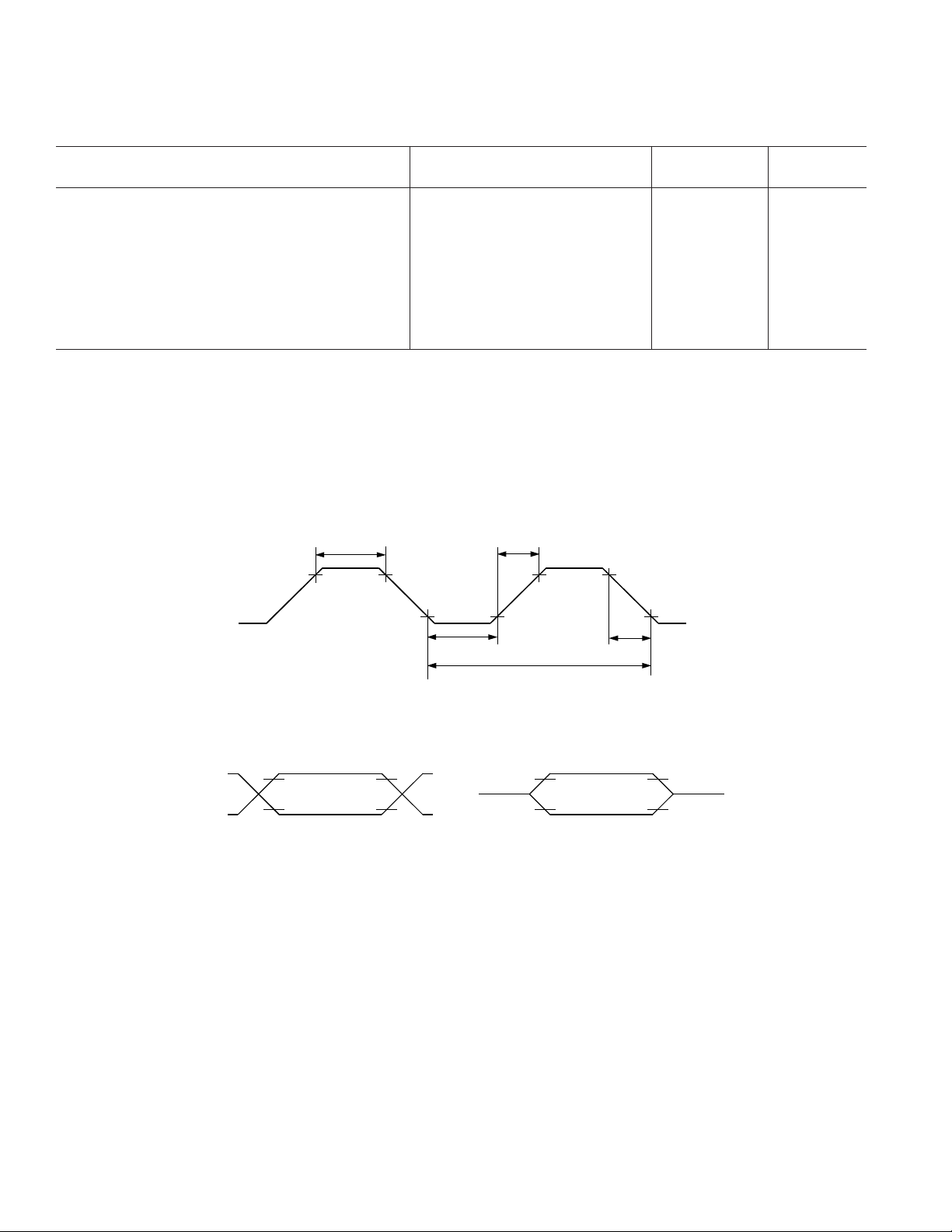
AC inputs during testing are driven at DVDD – 0.5 V for a Logic 1 and 0.45 V for a Logic 0. Timing measurements are made at VIH min for a Logic 1 and VIL max for
a Logic 0 as shown in Figure 2.
2
For timing purposes, a port pin is no longer floating when a 100 mV change from load voltage occurs. A port pin begins to float when a 100 mV change from the
loaded VOH/VOL level occurs as shown in Figure 2.
3
C
for Port0, ALE, PSEN outputs = 100 pF; C
LOAD
4
ADuC824 internal PLL locks onto a multiple (384 times) the external crystal frequency of 32.768 kHz to provide a Stable 12.583 MHz internal clock for the system.
The core can operate at this frequency or at a binary submultiple called Core_Clk, selected via the PLLCON SFR.
5
This number is measured at the default Core_Clk operating frequency of 1.57 MHz.
6
ADuC824 Machine Cycle Time is nominally defined as 12/Core_CLK.
XTAL1 Period 30.52 µs1
XTAL1 Width Low 15.24 µs1
XTAL1 Width High 15.24 µs1
XTAL1 Rise Time 20 ns 1
XTAL1 Fall Time 20 ns 1
ADuC824 Core Clock Frequency
ADuC824 Core Clock Period
ADuC824 Machine Cycle Time
LOAD
4
5
6
0.098 12.58 MHz
0.636 µs
0.95 7.6 122.45 µs
for all other outputs = 80 pF unless otherwise noted.
t
CHK
t
CKR
DVDD – 0.5V
0.45V
t
CKL
t
CK
Figure 1. XTAL1 Input
+ 0.9V
0.2DV
DD
TEST POINTS
0.2DV
DD –
0.1V
V
LOAD
V
LOAD
LOAD
+ 0.1V
– 0.1V
V
Figure 2. Timing Waveform Characteristics
TIMING
REFERENCE
POINTS
t
CKF
V
– 0.1V
V
LOAD
LOAD
+ 0.1V
V
LOAD
–8–
REV. B
ADuC824
12.58 MHz Core_Clk Variable Core_Clk
Parameter Min Max Min Max Unit Figure
EXTERNAL PROGRAM MEMORY
t
LHLL
t
AVLL
t
LLAX
t
LLIV
t
LLPL
t
PLPH
t
PLIV
t
PXIX
t
PXIZ
t
AVIV
t
PLAZ
t
PHAX
ALE Pulsewidth 119 2t
Address Valid to ALE Low 39 t
Address Hold after ALE Low 49 t
ALE Low to Valid Instruction In 218 4t
ALE Low to PSEN Low 49 t
PSEN Pulsewidth 193 3t
PSEN Low to Valid Instruction In 133 3t
Input Instruction Hold after PSEN 00 ns3
Input Instruction Float after PSEN 54 t
Address to Valid Instruction In 292 5t
PSEN Low to Address Float 25 25 ns 3
Address Hold after PSEN High 0 0 ns 3
CORE_CLK
t
LHLL
– 40 ns 3
CORE
– 40 ns 3
CORE
– 30 ns 3
CORE
– 30 ns 3
CORE
– 45 ns 3
CORE
– 100 ns 3
CORE
– 105 ns 3
CORE
– 25 ns 3
CORE
– 105 ns 3
CORE
ALE (O)
PSEN (O)
PORT 0 (I/O)
PORT 2 (O)
PLAZ
PCH
t
PLPH
t
LLIV
t
PLIV
t
PXIX
INSTRUCTION
(IN)
t
AVLL
PCL
(OUT)
t
LLPL
t
LLAX
t
t
AVIV
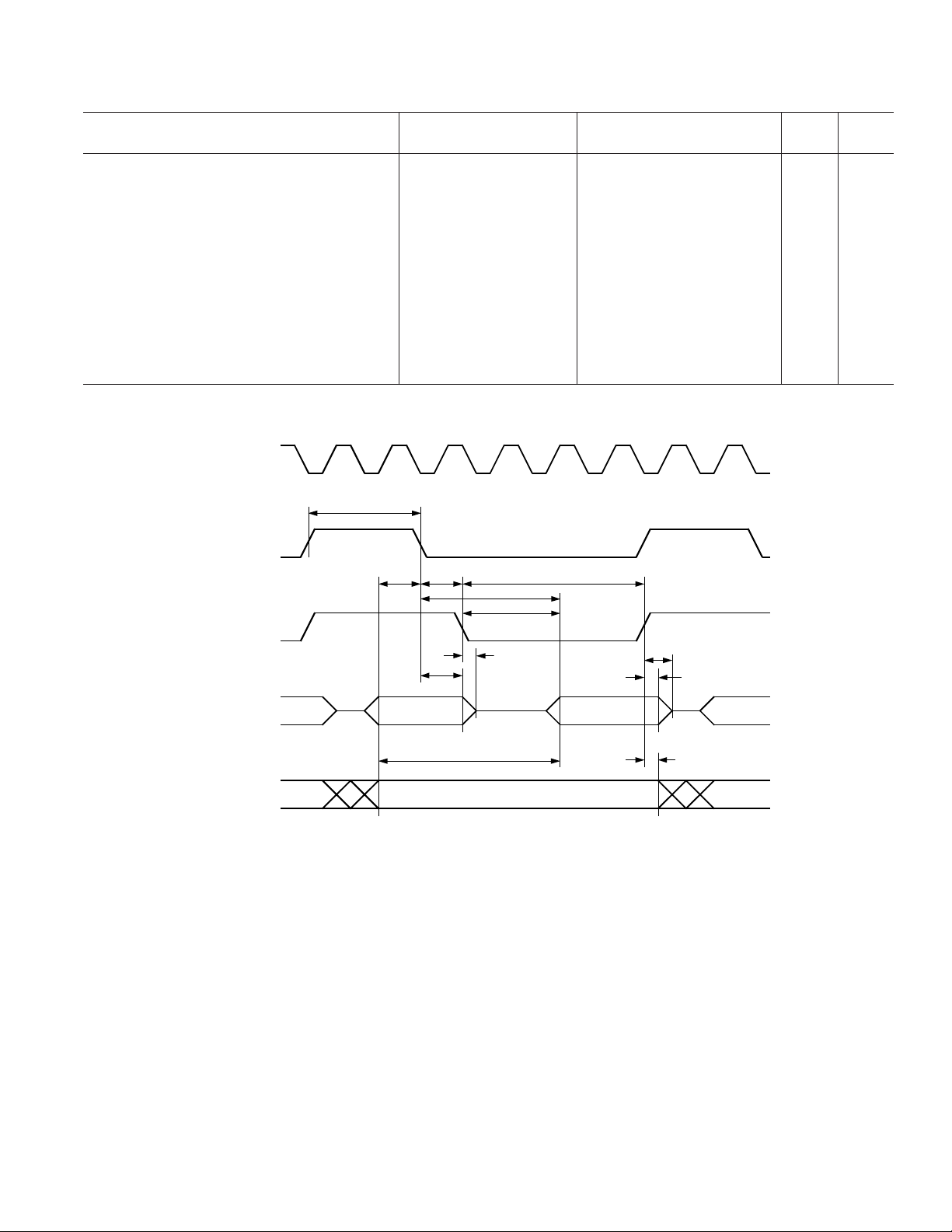
Figure 3. External Program Memory Read Cycle
t
PXIZ
t
PHAX
REV. B
–9–
ADuC824
12.58 MHz Core_Clk Variable Core_Clk
Parameter Min Max Min Max Unit Figure
EXTERNAL DATA MEMORY READ CYCLE
t
RLRH
t
AVLL
t
LLAX
t
RLDV
t
RHDX
t
RHDZ
t
LLDV
t
AVDV
t
LLWL
t
AVWL
t
RLAZ
t
WHLH
RD Pulsewidth 377 6t
Address Valid after ALE Low 39 t
Address Hold after ALE Low 44 t
RD Low to Valid Data In 232 5t
Data and Address Hold after RD 00 ns4
Data Float after RD 89 2t
ALE Low to Valid Data In 486 8t
Address to Valid Data In 550 9t
ALE Low to RD Low 188 288 3t
Address Valid to RD Low 188 4t
RD Low to Address Float 0 0 ns 4
RD High to ALE High 39 119 t
CORE_CLK
ALE (O)
– 100 ns 4
CORE
– 40 ns 4
CORE
– 35 ns 4
CORE
– 50 3t
CORE
– 130 ns 4
CORE
– 40 t
CORE
– 165 ns 4
CORE
– 70 ns 4
CORE
– 150 ns 4
CORE
– 165 ns 4
CORE
+ 50 ns 4
CORE
+ 40 ns 4
CORE
PSEN (O)
RD (O)
PORT 0 (I/O)
PORT 2 (O)
t
LLDV
t
AVLL
t
LLAX
A0–A7
(OUT)
t
AVDV
A16–A23
t
AVWL
t
LLWL
t
RLAZ
t
RLDV
A8–A15
t
RLRH
t
RHDX
DATA (IN)
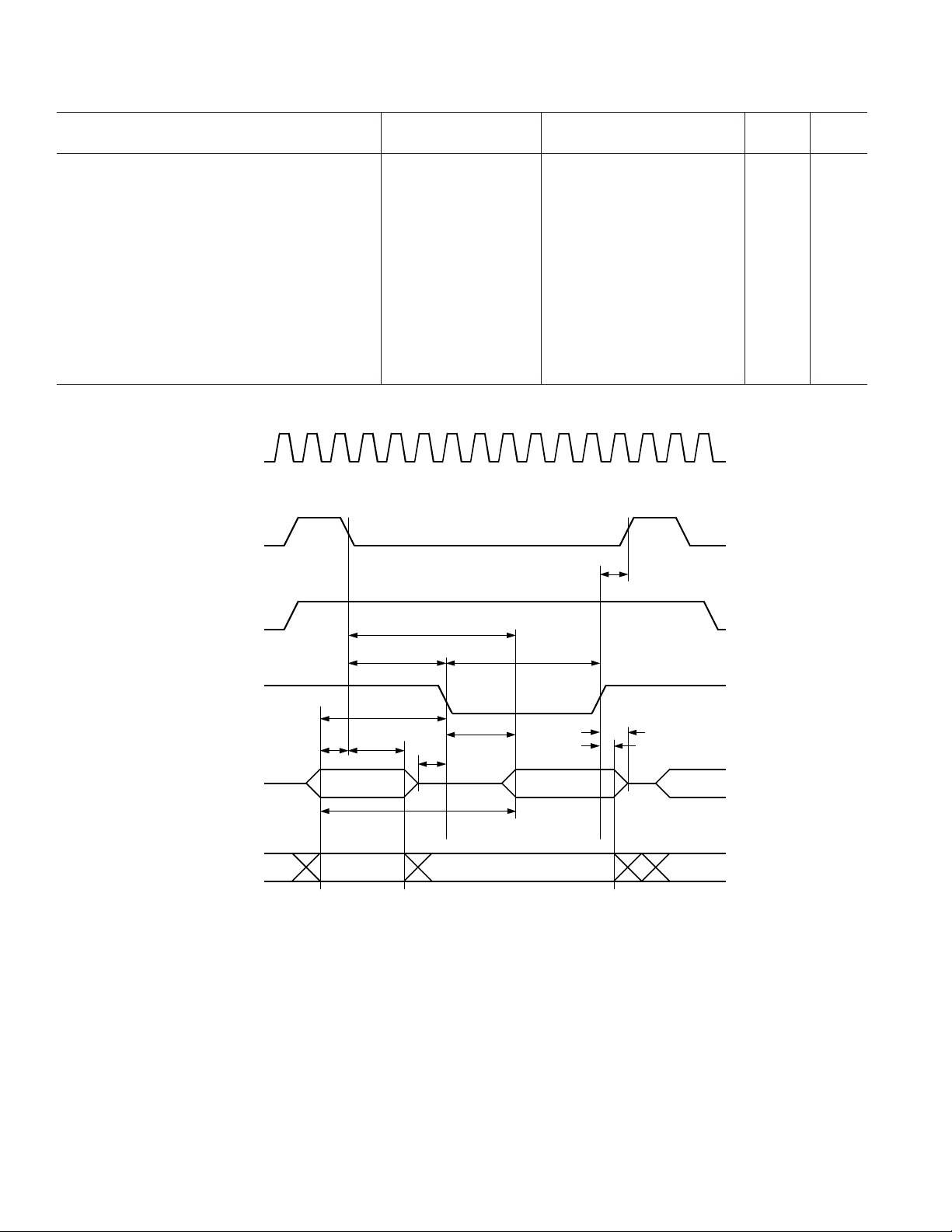
Figure 4. External Data Memory Read Cycle
t
WHLH
t
RHDZ
–10–
REV. B
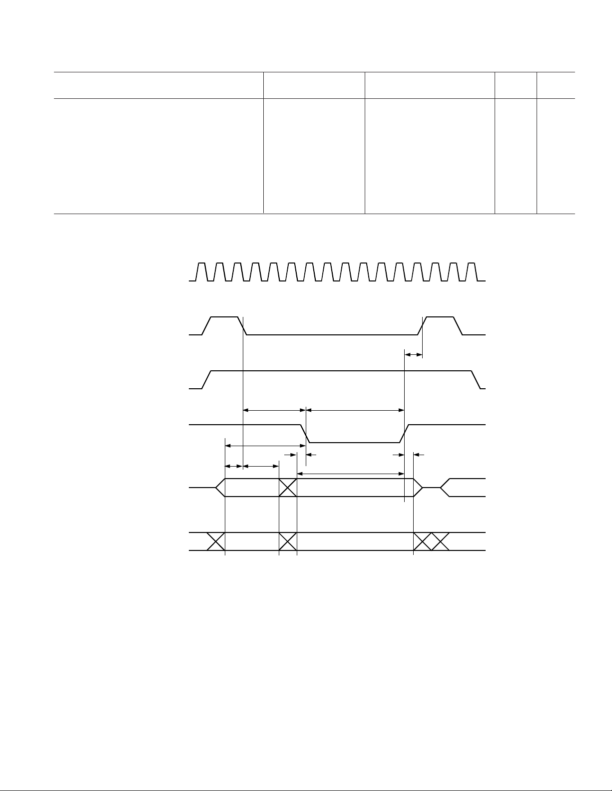
ADuC824
12.58 MHz Core_Clk Variable Core_Clk
Parameter Min Max Min Max Unit Figure
EXTERNAL DATA MEMORY WRITE CYCLE
t
WLWH
t
AVLL
t
LLAX
t
LLWL
t
AVWL
t
QVWX
t
QVWH
t
WHQX
t
WHLH
WR Pulsewidth 377 6t
Address Valid after ALE Low 39 t
Address Hold after ALE Low 44 t
ALE Low to WR Low 188 288 3t
Address Valid to WR Low 188 4t
Data Valid to WR Transition 29 t
Data Setup before WR 406 7t
Data and Address Hold after WR 29 t
WR High to ALE High 39 119 t
CORE_CLK
ALE (O)
– 100 ns 5
CORE
– 40 ns 5
CORE
– 35 ns 5
CORE
– 50 3t
CORE
– 130 ns 5
CORE
– 50 ns 5
CORE
– 150 ns 5
CORE
– 50 ns 5
CORE
– 40 t
CORE
+ 50 ns 5
CORE
+ 40 ns 5
CORE
PSEN (O)
WR (O)
PORT 0 (O)
PORT 2 (O)
t
QVWX
t
t
QVWH
DATA
A8–A15
WLWH
t
AVLL
t
LLAX
A0–A7
A16–A23
t
AVWL
t
LLWL
Figure 5. External Data Memory Write Cycle
t
WHLH
t
WHQX
REV. B
–11–
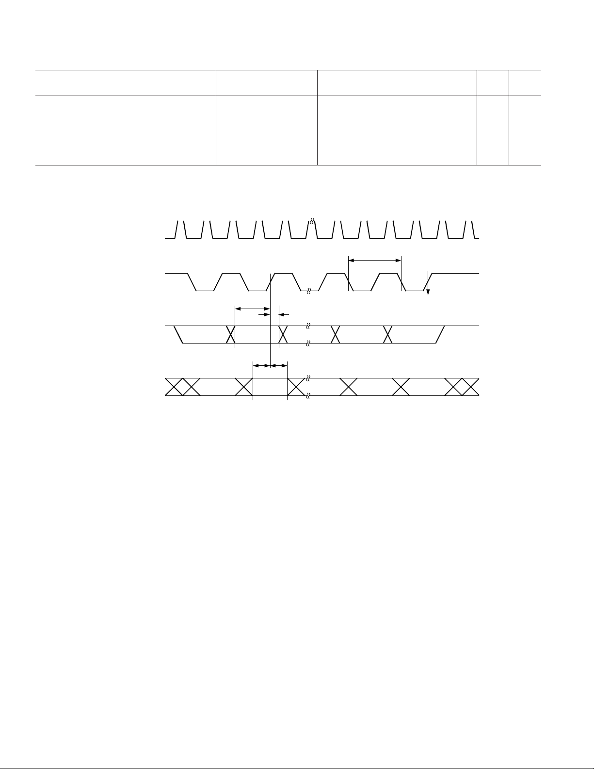
ADuC824
12.58 MHz Core_Clk Variable Core_Clk
Parameter Min Typ Max Min Typ Max Unit Figure
UART TIMING (Shift Register Mode)
t
XLXL
t
QVXH
t
DVXH
t
XHDX
t
XHQX
Serial Port Clock Cycle Time 0.95 12t
Output Data Setup to Clock 662 10t
Input Data Setup to Clock 292 2t
– 133 ns 6
CORE
+ 133 ns 6
CORE
CORE
Input Data Hold after Clock 0 0 ns 6
Output Data Hold after Clock 42 2t
ALE (O)
– 117 ns 6
CORE
t
XLXL
µs6
(OUTPUT CLOCK)
(OUTPUT DATA)
TXD
RXD
RXD
(INPUT DATA)
01
MSB
MSB
67
t
t
QVXH
BIT 6
DVXH
t
XHQX
t
XHDX
BIT 6 BIT 1
BIT 1
Figure 6. UART Timing in Shift Register Mode
SET RI
OR
SET TI
LSB
–12–
REV. B
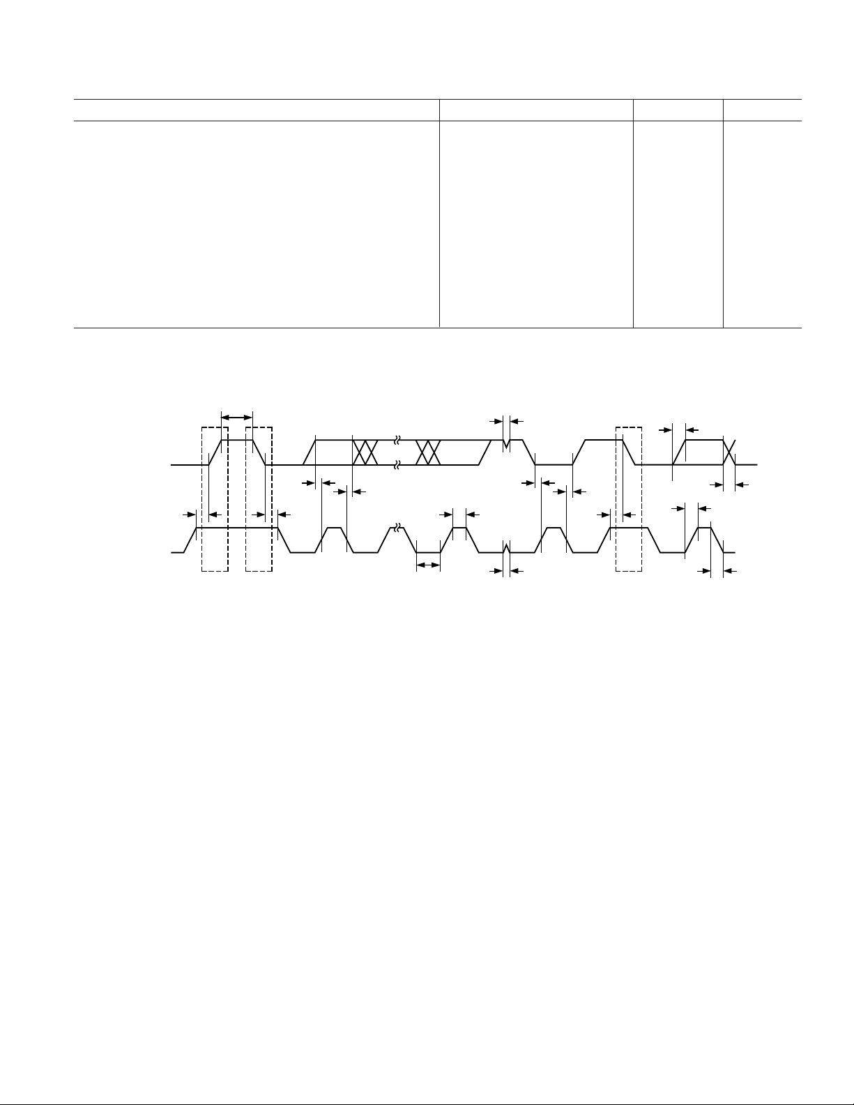
ADuC824
Parameter Min Max Unit Figure
2
I
C-COMPATIBLE INTERFACE TIMING
t
L
t
H
t
SHD
t
DSU
t
DHD
t
RSU
t
PSU
t
BUF
t
R
t
F
t
* Pulsewidth of Spike Suppressed 50 ns 7
SUP
*Input filtering on both the SCLOCK and SDATA inputs suppresses noise spikes less than 50 ns.
SCLOCK Low Pulsewidth 4.7 µs7
SCLOCK High Pulsewidth 4.0 µs7
Start Condition Hold Time 0.6 µs7
Data Setup Time 100 µs7
Data Hold Time 0.9 µs7
Setup Time for Repeated Start 0.6 µs7
Stop Condition Setup Time 0.6 µs7
Bus Free Time between a STOP 1.3 µs7
Condition and a START Condition
Rise Time of Both SCLOCK and SDATA 300 ns 7
Fall Time of Both SCLOCK and SDATA 300 ns 7
t
SDATA (I/O)
BUF
MSB
LSB
t
SUP
t
ACK MSB
R
SCLK (I)
t
PSU
PS
STOP
CONDITION
START
CONDITION
t
DSU
t
SHD
t
DHD
1 2-7
t
H
8
t
t
L
SUP
Figure 7. I2C-Compatible Interface Timing
t
DSU
t
t
DHD
t
RSU
9
S(R)
REPEATED
START
F
t
R
1
t
F
REV. B
–13–
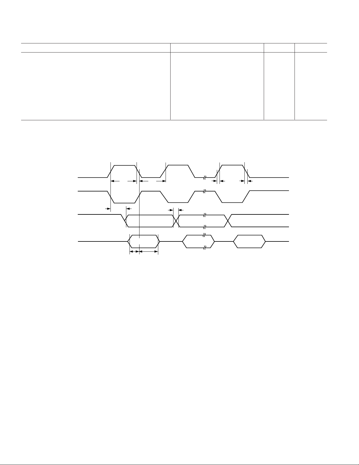
ADuC824
Parameter Min Typ Max Unit Figure
SPI MASTER MODE TIMING (CPHA = 1)
t
SL
t
SH
t
DAV
t
DSU
t
DHD
t
DF
t
DR
t
SR
t
SF
*Characterized under the following conditions:
a. Core clock divider bits CD2, CD1, and CD0 bits in PLLCON SFR set to 0, 1, and 1 respectively, i.e., core clock frequency = 1.57 MHz and
b. SPI bit-rate selection bits SPR1 and SPR0 bits in SPICON SFR set to 0 and 0 respectively.
SCLOCK Low Pulsewidth* 630 ns 8
SCLOCK High Pulsewidth* 630 ns 8
Data Output Valid after SCLOCK Edge 50 ns 8
Data Input Setup Time before SCLOCK Edge 100 ns 8
Data Input Hold Time after SCLOCK Edge 100 ns 8
Data Output Fall Time 10 25 ns 8
Data Output Rise Time 10 25 ns 8
SCLOCK Rise Time 10 25 ns 8
SCLOCK Fall Time 10 25 ns 8
SCLOCK
(CPOL = 0)
SCLOCK
(CPOL = 1)
t
SH
t
SL
t
SR
t
SF
MOSI
MISO
t
DAV
t
MSB IN
DSU
t
DHD
t
DF
t
DR
BITS 6–1
BITS 6–1
Figure 8. SPI Master Mode Timing (CPHA = 1)
LSBMSB
LSB IN
–14–
REV. B
ADuC824
Parameter Min Typ Max Unit Figure
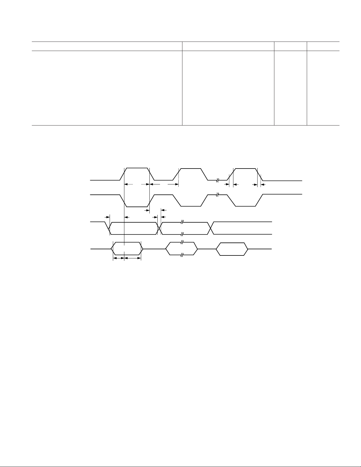
SPI MASTER MODE TIMING (CPHA = 0)
t
SL
t
SH
t
DAV
t
DOSU
t
DSU
t
DHD
t
DF
t
DR
t
SR
t
SF
*Characterized under the following conditions:
a. Core clock divider bits CD2, CD1, and CD0 bits in PLLCON SFR set to 0, 1, and 1 respectively, i.e., core clock frequency = 1.57 MHz and
b. SPI bit-rate selection bits SPR1 and SPR0 bits in SPICON SFR set to 0 and 0 respectively.
SCLOCK Low Pulsewidth* 630 ns 9
SCLOCK High Pulsewidth* 630 ns 9
Data Output Valid after SCLOCK Edge 50 ns 9
Data Output Setup before SCLOCK Edge 150 ns 9
Data Input Setup Time before SCLOCK Edge 100 ns 9
Data Input Hold Time after SCLOCK Edge 100 ns 9
Data Output Fall Time 10 25 ns 9
Data Output Rise Time 10 25 ns 9
SCLOCK Rise Time 10 25 ns 9
SCLOCK Fall Time 10 25 ns 9
SCLOCK
(CPOL = 0)
SCLOCK
(CPOL = 1)
t
SH
t
SL
t
SR
t
SF
MOSI
MISO
t
DAV
t
DOSU
t
DSU
MSB IN
MSB
t
DHD
t
DF
t
DR
BITS 6–1
BITS 6–1
Figure 9. SPI Master Mode Timing (CPHA = 0)
LSB
LSB IN
REV. B
–15–
ADuC824
Parameter Min Typ Max Unit Figure
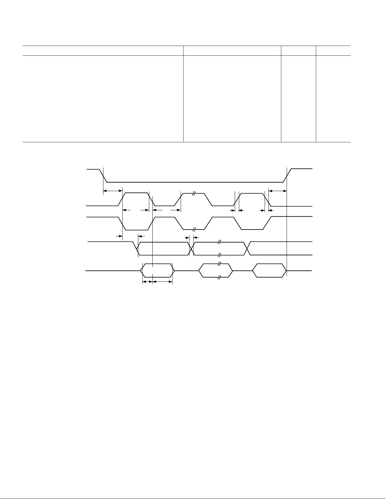
SPI SLAVE MODE TIMING (CPHA = 1)
t
SS
t
SL
t
SH
t
DAV
t
DSU
t
DHD
t
DF
t
DR
t
SR
t
SF
t
SFS
SS to SCLOCK Edge 0 ns 10
SCLOCK Low Pulsewidth 330 ns 10
SCLOCK High Pulsewidth 330 ns 10
Data Output Valid after SCLOCK Edge 50 ns 10
Data Input Setup Time before SCLOCK Edge 100 ns 10
Data Input Hold Time after SCLOCK Edge 100 ns 10
Data Output Fall Time 10 25 ns 10
Data Output Rise Time 10 25 ns 10
SCLOCK Rise Time 10 25 ns 10
SCLOCK Fall Time 10 25 ns 10
SS High after SCLOCK Edge 0 ns 10
SS
SCLOCK
(CPOL = 0)
SCLOCK
(CPOL = 1)
MISO
MOSI
t
SS
MSB IN
MSB
t
DHD
t
SL
t
DF
t
DR
BITS 6
BITS 6
t
SH
t
DAV
t
DSU
Figure 10. SPI Slave Mode Timing (CPHA = 1)
t
SR
–
1
–
1 LSB IN
t
SF
LSB
t
SFS
–16–
REV. B
ADuC824
Parameter Min Typ Max Unit Figure
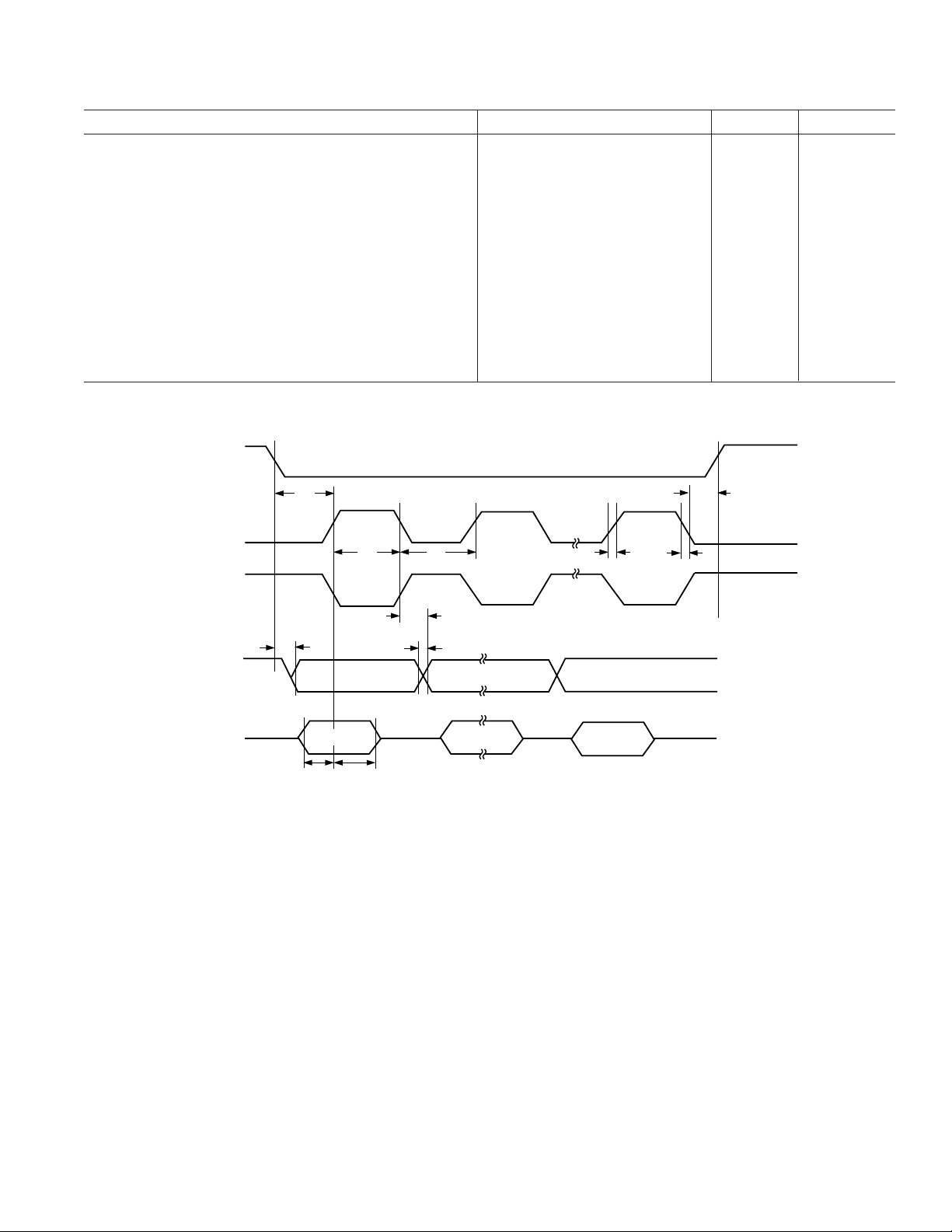
SPI SLAVE MODE TIMING (CPHA = 0)
t
SS
t
SL
t
SH
t
DAV
t
DSU
t
DHD
t
DF
t
DR
t
SR
t
SF
t
SSR
t
DOSS
t
SFS
SS to SCLOCK Edge 0 ns 11
SCLOCK Low Pulsewidth 330 ns 11
SCLOCK High Pulsewidth 330 ns 11
Data Output Valid after SCLOCK Edge 50 ns 11
Data Input Setup Time before SCLOCK Edge 100 ns 11
Data Input Hold Time after SCLOCK Edge 100 ns 11
Data Output Fall Time 10 25 ns 11
Data Output Rise Time 10 25 ns 11
SCLOCK Rise Time 10 25 ns 11
SCLOCK Fall Time 10 25 ns 11
SS to SCLOCK Edge 50 ns 11
Data Output Valid after SS Edge 20 ns 11
SS High after SCLOCK Edge 0 ns 11
SS
t
SFS
t
SF
SCLOCK
(CPOL = 0)
SCLOCK
(CPOL = 1)
MISO
t
DOSS
t
SS
MSB
t
SH
t
t
SL
t
DAV
DF
t
DR
BITS 6–1
t
SR
LSB
MOSI
BITS 6–1
t
DSU
MSB IN
t
DHD
Figure 11. SPI Slave Mode Timing (CPHA = 0)
LSB IN
REV. B
–17–
ADuC824
WARNING!
ESD SENSITIVE DEVICE
ABSOLUTE MAXIMUM RATINGS
(TA = 25°C unless otherwise noted.)
1
AVDD to AGND . . . . . . . . . . . . . . . . . . . . . . . –0.3 V to +7 V
to DGND . . . . . . . . . . . . . . . . . . . . . . . –0.3 V to +7 V
AV
DD
DV
to AGND . . . . . . . . . . . . . . . . . . . . . . . –0.3 V to +7 V
DD
DV
to DGND . . . . . . . . . . . . . . . . . . . . . . . –0.3 V to +7 V
DD
AGND to DGND
AV
to DVDD . . . . . . . . . . . . . . . . . . . . . . . . . –2 V to +5 V
DD
Analog Input Voltage to AGND
Reference Input Voltage to AGND . . –0.3 V to AV
2
. . . . . . . . . . . . . . . . . . . –0.3 V to +0.3 V
3
. . . . –0.3 V to AVDD + 0.3 V
+ 0.3 V
DD
AIN/REFIN Current (Indefinite) . . . . . . . . . . . . . . . . 30 mA
Digital Input Voltage to DGND . . . –0.3 V to DV
Digital Output Voltage to DGND . . –0.3 V to DV
+ 0.3 V
DD
+ 0.3 V
DD
Operating Temperature Range . . . . . . . . . . . –40°C to +85°C
Storage Temperature Range . . . . . . . . . . . . –65°C to +150°C
Junction Temperature . . . . . . . . . . . . . . . . . . . . . . . . . 150°C
θJA Thermal Impedance . . . . . . . . . . . . . . . . . . . . . . . 90°C/W
Lead Temperature, Soldering
Vapor Phase (60 sec) . . . . . . . . . . . . . . . . . . . . . . . . 215°C
Infrared (15 sec) . . . . . . . . . . . . . . . . . . . . . . . . . . . 220°C
NOTES
1
Stresses above those listed under Absolute Maximum Ratings may cause perma-
nent damage to the device. This is a stress rating only; functional operation of the
device at these or any other conditions above those listed in the operational
sections of this specification is not implied. Exposure to absolute maximum rating
conditions for extended periods may affect device reliability.
2
AGND and DGND are shorted internally on the ADuC824.
3
Applies to P1.2 to P1.7 pins operating in analog or digital input modes.
ORDERING GUIDE
Temperature Package Package
Model Range Description Option
ADuC824BS –40°C to +85°C 52-Lead Plastic S-52
Quad Flatpack
QuickStart
Development
System Model Description
EVAL-ADUC824QS Development System for the ADuC824
MicroConverter, containing:
Evaluation Board
Serial Port Cable
Plug-In Power Supply
Windows
®
Serial Downloader (WSD)*
Windows Debugger (DeBug)
Windows ADuC824 Simulator
(ADSIM)
Windows ADC Analysis Software
Program (WASP)
8051 Assembler (Metalink)
C-Compiler (Keil) Evaluation Copy
Limited to 2 Kcode
Example Code
Documentation
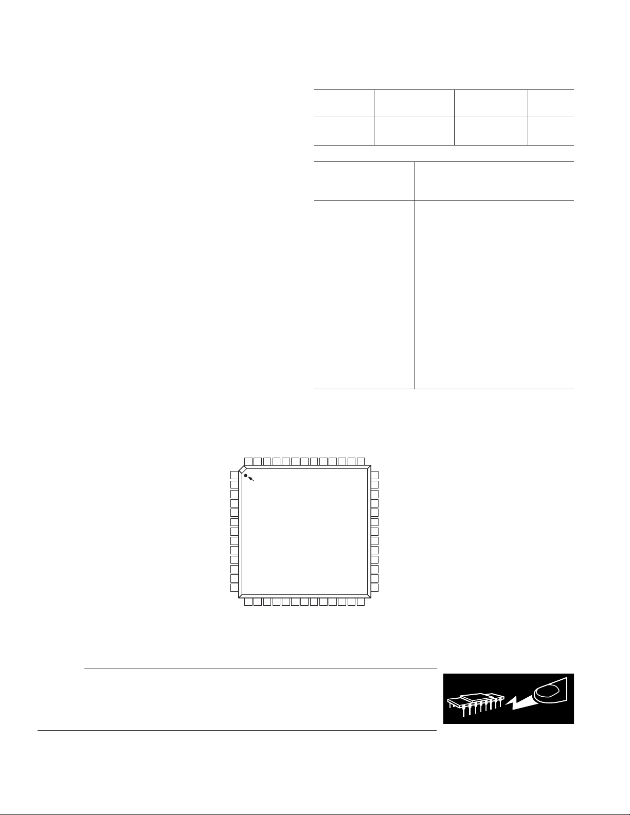
PIN CONFIGURATION
52 51 50 49 48 43 42 41 4047 46 45 44
1
PIN 1
2
IDENTIFIER
3
4
5
6
7
8
9
10
11
12
13
14 15 16 17 18 19 20 21 22 23 24 25 26
ADuC824
TOP VIEW
(Not to Scale)
39
38
37
36
35
34
33
32
31
30
29
28
27
CAUTION
ESD (electrostatic discharge) sensitive device. Electrostatic charges as high as 4000 V readily
accumulate on the human body and test equipment and can discharge without detection. Although
the ADuC824 features proprietary ESD protection circuitry, permanent damage may occur on
devices subjected to high energy electrostatic discharges. Therefore, proper ESD precautions are
recommended to avoid performance degradation or loss of functionality.
*Windows is a registered trademark of Microsoft Corporation.
–18–
REV. B

ADuC824
PIN FUNCTION DESCRIPTIONS
Pin
No. Mnemonic Type* Description
1 P1.0/T2 I/O Port 1.0 can function as a digital input or digital output and has a pull-up configuration as
described below for Port 3. P1.0 has an increased current drive sink capability of 10 mA and can
also be used to provide a clock input to Timer 2. When Enabled, Counter 2 is incremented in
response to a negative transition on the T2 input pin.
2 P1.1/T2EX I/O Port 1.1 can function as a digital input or digital output and has a pull-up configuration as
described below for Port 3. P1.1 has an increased current drive sink capability of 10 mA and
can also be used to provide a control input to Timer 2. When Enabled, a negative transition on
the T2EX input pin will cause a Timer 2 capture or reload event.
3 P1.2/DAC/IEXC1 I/O Port 1.2. This pin has no digital output driver; it can function as a digital input for which ‘0’
must be written to the port bit. As a digital input, P1.2 must be driven high or low externally.
The voltage output from the DAC can also be configured to appear at this pin. If the DAC
output is not being used, one or both of the excitation current sources (200 µA or 2 × 200 µA)
can be programmed to be sourced at this pin.
4 P1.3/AIN5/IEXC2 I Port 1.3. This pin has no digital output driver; it can function as a digital input for which ‘0’ must
be written to the port bit. As a digital input, P1.3 must be driven high or low externally. This
pin can provide an analog input (AIN5) to the auxiliary ADC and one or both of the excitation
current sources (200 µA or 2 × 200 µA) can be programmed to be sourced at this pin.
5AV
6 AGND S Analog Ground. Ground reference pin for the analog circuitry
7 REFIN(–) I Reference Input, Negative Terminal
8 REFIN(+) I Reference Input, Positive Terminal
9–11 P1.4–P1.6 I Port 1.4 to P1.6. These pins have no digital output drivers; they can function as digital inputs,
12 P1.7/AIN4/DAC I/O Port 1.7. This pin has no digital output driver; it can function as a digital input for which ‘0’ must be
13 SS I Slave Select Input for the SPI Interface. A weak pull-up is present on this pin.
14 MISO I/O Master Input/Slave Output for the SPI Interface. There is a weak pull-up on this input pin.
15 RESET I Reset Input. A high level on this pin for 24 core clock cycles while the oscillator is running resets
16–19 P3.0–P3.3 I/O P3.0–P3.3 are bidirectional port pins with internal pull-up resistors. Port 3 pins that have 1s written
20, 34, 48 DV
21, 35, 47 DGND S Digital ground, ground reference point for the digital circuitry
DD
P1.4/AIN1 I Primary ADC Channel, Positive Analog Input
P1.5/AIN2 I Primary ADC Channel, Negative Analog Input
P1.6/AIN3 I Auxiliary ADC Input or muxed Primary ADC Channel, Positive Analog Input
P3.0/RXD I/O Receiver Data Input (asynchronous) or Data Input/Output (synchronous) of serial (UART) port.
P3.1/TXD I/O Transmitter Data Output (asynchronous) or Clock Output (synchronous) of serial (UART) port.
P3.2/INT0 I/O Interrupt 0, programmable edge or level triggered Interrupt input, which can be programmed
P3.3/INT1 I/O Interrupt 1, programmable edge-or level-triggered Interrupt input, which can be programmed
DD
S Analog Supply Voltage, 3 V or 5 V
for which ‘0’ must be written to the respective port bit. As a digital input, these pins must be
driven high or low externally. These port pins also have the following analog functionality:
written to the port bit. As a digital input, P1.7 must be driven high or low externally. This pin can
provide an analog input (AIN4) to the auxiliary ADC or muxed Primary ADC Channel, Negative
Analog Input. The voltage output from the DAC can also be configured to appear at this pin.
the device. There is a weak pull-down and a Schmitt trigger input stage on this pin. External
POR (power-on reset) circuitry must be added to drive the RESET pin as described later in
this data sheet.
to them are pulled high by the internal pull-up resistors, and in that state can be used as inputs.
As inputs, Port 3 pins being pulled externally low will source current because of the internal pull-up
resistors. When driving a 0-to-1 output transition, a strong pull-up is active for two core clock
periods of the instruction cycle. Port 3 pins also have various secondary functions described below.
to one of two priority levels. This pin can also be used as a gate control input to Timer0.
to one of two priority levels. This pin can also be used as a gate control input to Timer1.
S Digital supply, 3 V or 5 V
REV. B
–19–

ADuC824
PIN FUNCTION DESCRIPTIONS (continued)
Pin
No. Mnemonic Type* Description
22–25 P3.4–P3.7 I/O P3.4–P3.7 are bidirectional port pins with internal pull-up resistors. Port 3 pins that have 1s
written to them are pulled high by the internal pull-up resistors, and in that state can be used as
inputs. As inputs, Port 3 pins being pulled externally low will source current because of the
internal pull-up resistors. When driving a 0-to-1 output transition, a strong pull-up is active for
two core clock periods of the instruction cycle. The secondary functions of Port 3 pins are:
P3.4/T0 I/O Timer/Counter 0 Input
P3.5/T1 I/O Timer/Counter 1 Input
P3.6/WR I/O Write Control Signal, Logic Output. Latches the data byte from Port 0 into an external data memory.
P3.7/RD I/O Read Control Signal, Logic Output. Enables the data from an external data memory to Port 0.
26 SCLK I/O Serial interface clock for either the I
triggered input and a weak internal pull-up is present on this pin unless it is outputting logic low.
27 SDATA/MOSI I/O Serial data I/O for the I
2
C compatible interface or master output/slave input for the SPI interface.
A weak internal pull-up is present on this pin unless it is outputting logic low.
28 – 31 P2.0 – P2.3 I/O Port 2 is a bidirectional port with internal pull-up resistors. Port 2 pins that have 1s (A8–A11)
written to them are pulled high by the internal pull-up resistors, and in that state can (A16–A19)
be used as inputs. As inputs, Port 2 pins being pulled externally low will source current because
of the internal pull-up resistors. Port 2 emits the high order address bytes during fetches from
external program memory and middle and high order address bytes during accesses to the 24-bit
external data memory space.
32 XTAL1 I Input to the crystal oscillator inverter
33 XTAL2 O Output from the crystal oscillator inverter
36 – 39 P2.4 – P2.7 I/O Port 2 is a bidirectional port with internal pull-up resistors. Port 2 pins that have 1s (A12–A15)
written to them are pulled high by the internal pull-up resistors, and in that state they (A20–A23)
can be used as inputs. As inputs, Port 2 pins being pulled externally low will source current
because of the internal pull-up resistors. Port 2 emits the high order address bytes during fetches
from external program memory and middle and high order address bytes during accesses to the
24-bit external data memory space.
40 EA I/O External Access Enable, Logic Input. When held high, this input enables the device to fetch
code from internal program memory locations 0000H to 1FFFH. When held low, this input
enables the device to fetch all instructions from external program memory. To determine the
mode of code execution, i.e., internal or external, the EA pin is sampled at the end of an external
RESET assertion or as part of a device power cycle. EA may also be used as an external emula-
tion I/O pin and therefore the voltage level at this pin must not be changed during normal mode
operation as it may cause an emulation interrupt that will halt code execution.
41 PSEN O Program Store Enable, Logic Output. This output is a control signal that enables the external
program memory to the bus during external fetch operations. It is active every six oscillator
periods except during external data memory accesses. This pin remains high during internal
program execution. PSEN can also be used to enable serial download mode when pulled low
through a resistor at the end of an external RESET assertion or as part of a device power cycle.
42 ALE O Address Latch Enable, Logic Output. This output is used to latch the low byte (and page byte for
24-bit data address space accesses) of the address to external memory during external code or
data memory access cycles. It is activated every six oscillator periods except during an external
data memory access. It can be disabled by setting the PCON.4 bit in the PCON SFR.
43 – 46 P0.0 – P0.3 I/O P0.0 – P0.3 pins are part of Port 0, which is an 8-bit open-drain bidirectional.
(AD0 – AD3) I/O port. Port 0 pins that have 1s written to them float and in that state can be used as high impedance
inputs. An external pull-up resistor will be required on P0 outputsto force a valid logic high level
externally. Port 0 is also the multiplexed low-order address and data bus during accesses to external
program or data memory. In this application it uses strong internal pull-ups when emitting 1s.
49 – 52 P0.4 – P0.7 I/O P0.4 – P0.7 pins are part of Port 0, which is an 8-bit open drain bidirectional.
(AD4 – AD7) I/O port. Port 0 pins that have 1s written to them float and in that state can be used as high impedance
inputs. Port 0 is also the multiplexed low-order address and data bus during accesses to external
program or data memory. In this application it uses strong internal pull-ups when emitting 1s.
*I = Input, O = Output, S = Supply
NOTES
1. In the following descriptions, SET implies a Logic 1 state and CLEARED implies a Logic 0 state unless otherwise stated.
2. In the following descriptions, SET and CLEARED also imply that the bit is set or automatically cleared by the ADuC824 hardware unless otherwise stated.
3. User software should not write 1s to reserved or unimplemented bits as they may be used in future products.
–20–
2
C-compatible or SPI interface. As an input this pin is a Schmitt-
REV. B
ADuC824
AIN1
AIN2
AIN3
AIN4
AIN5
REFIN
REFIN
IEXC1
IEXC2
P0.0 (AD0)44P0.1 (AD1)45P0.2 (AD2)46P0.3 (AD3)49P0.4 (AD4)50P0.5 (AD5)
43
AIN
MUX
AIN
MUX
TEMP
SENSOR
P0.6 (AD6)52P0.7 (AD7)1P1.0 (T2)2P1.1 (T2EX)
51
BUF
AUXILIARY ADC
BANDGAP
REFERENCE
V
REF
DETECT
200A 200A
CURRENT
SOURCE
MUX
20
34
48
DV
21
DD
DD
DV
5
6
DD
DD
AV
DV
AGND
PGA
16-BIT
- ADC
ASYNCHRONOUS
SERIAL PORT
DGND35DGND47DGND
P1.2 (DAC/IEXC1)
P1.4 (AIN1)
P1.5 (AIN2)
P1.3 (AIN5/IEXC2)
3
4 9
10
PRIMARY ADC
24-BIT
- ADC
ADC CONTROL
AND
CALIBRATION
6408
DATA
FLASH/EE
8K8
PROGRAM
FLASH/EE
DOWNLOADER
DEBUGGER
(UART)
17
16
TXD
RXD
P1.6 (AIN3)
P1.7 (AIN4/DAC)
11
12
42
P2.0 (A8/A16)29P2.1 (A9/A17)
P2.2 (A10/A18)31P2.3 (A11/A19)
28
30
ADC CONTROL
AND
CALIBRATION
8052
MCU
CORE
EMULATOR
SINGLE-PIN
15
40EA41
ALE
PSEN
RESET
P2.4 (A12/A20)37P2.5 (A13/A21)38P2.6 (A14/A22)39P2.7 (A15/A23)16P3.0 (RXD)
36
P3.1 (TXD)18P3.2 (INT0)19P3.3 (INT1)22P3.4 (T0)23P3.5 (T1)24P3.6 (WR)25P3.7 (RD)
17
ADuC824
2568
TIMER
14
MISO
12-BIT
VOLTAGE
OUTPUT DAC
2
C)
13
SS
DAC
CONTROL
USER RAM
WATCHDOG
POWER SUPPLY
MONITOR
SYNCHRONOUS
SERIAL INTERFACE
(SPI OR I
26
27
SCLK
16-BIT
COUNTER
TIMERS
INTERVAL
COUNTER
PROG.
CLOCK
DIVIDER
OSC
AND
PLL
32
TIME
33
XTAL1
BUF
XTAL2
3
DAC
22
T0
T1
23
1
T2
2
T2EX
INT0
18
19
INT1
Figure 12. Block Diagram
SDATA/MOSI
REV. B
–21–
 Loading...