

MicroConverter®, Small Package
12-Bit ADC with Embedded Flash MCU
ADuC814
FEATURES
ANALOG I/O
6-channel 247 kSPS ADC
AIN0
12-bit resolution
ADC high speed data capture mode
AIN5
Programmable reference via on-chip DAC for low
level inputs, ADC performance specified to V
REF
= 1 V
Dual voltage output DACs
12-bit resolution, 15 µs settling time
Memory
8 kbytes on-chip Flash/EE program memory
V
REF
640 bytes on-chip Flash/EE data memory
Flash/EE, 100 year retention, 100 kcycle endurance
C
REF
3 levels of Flash/EE program memory security
In-circuit serial downlaod (no external hardware)
256 bytes on-chip data RAM
8051 based core
8051 compatible instruction set
32 kHz external crystal,
on-chip programmable PLL (16.78 MHz max)
Three 16-bit timer/counters
11 programmable I/O lines
11 interrupt sources, 2 priority levels
Power
Specified for 3 V and 5 V operation
Normal: 3 mA @ 3 V (core CLK = 2.1 MHz)
Power-down: 15 µA (32 kHz oscillator running)
On-chip peripherals
Power-on reset circuit (no need for external POR device)
Temperature monitor (±1.5°C accuracy)
Precision voltage reference
Time interval counter (wake-up/RTC timer)
UART serial I/O
2
C® compatible serial I/O
SPI®/I
Watchdog timer (WDT), power supply monitor (PSM)
Package and temperature range
28-lead TSSOP 4.4 mm × 9.7 mm package
Fully specified for −40°C to +125°C operation
APPLICATIONS
Optical networking—laser power control
Base station systems—power amplifier bias control
Precision instruments, smart sensors
Battery-powered systems, precision system monitors
Rev. A
Information furnished by Analog Devices is believed to be accurate and reliable.
However, no responsibility is assumed by Analog Devices for its use, nor for any
infringements of patents or other rights of third parties that may result from its use.
Specifications subject to change without notice. No license is granted by implication
or otherwise under any patent or patent rights of Anal og Devices. Trademarks and
registered trademarks are the property of their respective owners.
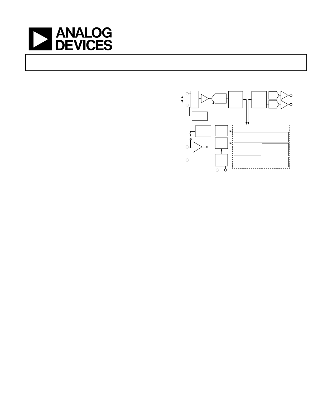
GENERAL DESCRIPTION
The ADuC814 is a fully integrated 247 kSPS, 12-bit data acquisition system incorporating a high performance multichannel
ADC, an 8-bit MCU, and program/data Flash/EE memory on a
single chip.
This low power device operates from a 32 kHz crystal with an
on-chip PLL generating a high frequency clock of 16.78 MHz.
This clock is, in turn, routed through a programmable clock
divider from which the MCU core clock operating frequency is
generated.
The microcontroller core is an 8052 and is compatible with an
8051 instruction. 8 kBytes of nonvolatile Flash/EE program
memory are provided on-chip. 640 bytes of nonvolatile Flash/EE
data memory and 256 bytes RAM are also integrated on-chip.
The ADuC814 also incorporates additional analog functionality
with dual 12-bit DACs, a power supply monitor, and a band gap
reference. On-chip digital peripherals include a watchdog timer,
time interval counter, three timer/counters, and two serial I/O
ports (SPI and UART).
On-chip factory firmware supports in-circuit serial download
and debug modes (via UART), as well as single-pin emulation
mode via the DLOAD pin. The ADuC814 is supported by a
QuickStart™ Development System.
The part operates from a single 3 V or 5 V supply over the
extended temperature range −40°C to +125°C. When operating
from 3 V supplies, the power dissipation for the part is below
10 mW. The ADuC814 is housed in a 28-lead TSSOP package.
One Technology Way, P.O. Box 9106, Norwood, MA 02062-9106, U.S.A.
Tel: 781.329.4700
Fax: 781.326.8703 © 2003 Analog Devices, Inc. All rights reserved.
FUNCTIONAL BLOCK DIAGRAM
ADuC814
DAC
CONTROL
LOGIC
PERIPHERALS
256 BYTES USER RAM
3 × 16-BIT
TIMER
I/O PINS
ON-CHIP MONITORS
WATCHDOG TIMER
ON
RESET
PROG.
CLOCK
OSC
AND
PLL
XTAL2XTAL1
ADC
CONTROL
LOGIC
8051-BASED MCU WITH ADDITIONAL
8 KBYTES FLASH/EE PROGRAM MEMORY
640 BYTES FLASH/EE DATA MEMORY
TIMER/COUNTERS
1 × WAKE-UP/RTC
10 × DIGITAL
AIN
MUX
TEMP
MONITOR
INTERNAL
BAND GAP
BUF
12-BIT
T/H
ADC
POWER-
V
REF
DIVIDER
Figure 1.
www.analog.com
DAC0
BUF
DAC1
BUF
POWER SUPPLY
MONITOR
UART AND SPI
SERIAL I/O
DAC0
DAC1
02748-A-001

ADuC814
TABLE OF CONTENTS
Specifications..................................................................................... 4
Absolute Maximum Ratings............................................................ 9
ESD Caution.................................................................................. 9
Pin Configuration and Function Description ............................10
Terminology .................................................................................... 12
ADC Specifications ....................................................................12
DAC Specifications..................................................................... 12
Typical Performance Curves......................................................... 13
ADuC814 Architecture, Main Features ....................................... 16
Memory Organization ............................................................... 17
Overview of MCU-Related SFRs.............................................. 18
Accumulator SFR ................................................................... 18
B SFR........................................................................................ 18
Stack Pointer SFR ...................................................................18
Data Pointer ............................................................................18
ADC Offset and Gain Calibration Overview ......................... 28
ADC Offset and Gain Calibration Coefficients..................... 28
Calibrating the ADC.................................................................. 29
Initiating Calibration in Code .................................................. 29
Nonvolitile Flash/EE Memory ...................................................... 30
Flash/EE Memory Overview .................................................... 30
Flash/EE Memory and the ADuC814...................................... 30
ADuC814 Flash/EE Memory Reliability................................. 30
Using Flash/EE Program Memory........................................... 31
Serial Downloading (In-Circuit Programming)................ 31
Parallel Programming............................................................ 31
Flash/EE Program Memory Security....................................... 31
Lock Mode .............................................................................. 31
Secure Mode ........................................................................... 31
Serial Safe Mode ..................................................................... 31
Program Status Word SFR..................................................... 18
Power Control SFR................................................................. 19
Special Function Registers ........................................................ 20
ADC Circuit Information.............................................................. 21
General Overview....................................................................... 21
ADC Transfer Function............................................................. 21
ADC Data Output Format.................................................... 21
SFR Interface to ADC Block ..................................................... 22
ADCCON1 (ADC Control SFR 1) .......................................... 22
ADCCON2 (ADC Control SFR 2) .......................................... 23
ADCCON3 (ADC Control SFR 3) .......................................... 24
Driving the ADC............................................................................. 25
Voltage Reference Connections................................................ 26
Configuring the ADC ................................................................26
Initiating ADC Conversions ..................................................... 27
Using Flash/EE Data Memory.................................................. 32
ECON—Flash/EE Memory Control SFR ........................... 32
Flash/EE Memory Timing ........................................................ 33
Using the Flash/EE Memory Interface................................ 33
Programming a Byte.............................................................. 33
User Interface to Other On-Chip ADuC814 Peripherals.......... 34
DACs............................................................................................ 34
Using the DACs...................................................................... 35
On-Chip PLL .............................................................................. 37
Time Interval Counter (TIC).................................................... 38
Watchdog Timer......................................................................... 41
Power Supply Monitor............................................................... 42
ADuC814 Configuration Register (CFG814) ........................ 43
Serial Peripheral Interface..................................................... 43
External Clock ........................................................................ 43
ADC High Speed Data Capture Mode .................................... 27
Rev. A | Page 2 of 72

ADuC814
Serial Peripheral Interface..........................................................44
SBUF.........................................................................................53
MISO (Master In, Slave Out Data I/O Pin).........................44
MOSI (Master Out, Slave In Pin)..........................................44
SCLOCK (Serial Clock I/O Pin) ...........................................44
SS
(Slave Select Input Pin).....................................................44
Using the SPI Interface...........................................................45
SPI Interface—Master Mode .................................................45
SPI Interface—Slave Mode ....................................................45
2
I
C Compatible Interface............................................................46
8051 Compatible On-Chip Peripherals....................................47
Parallel I/O Ports 1 and 3.......................................................47
Additional Digital Outputs Pins ...........................................47
Timers/Counters.........................................................................48
Timer/Counter 0 and 1 Data Registers................................49
Timer/Counter 0 and 1 Operating Modes...............................50
Mode 0 (13-Bit Timer/Counter)...........................................50
Mode 0: 8-Bit Shift Register Mode.......................................54
Mode 1: 8-Bit UART, Variable Baud Rate ............................54
Mode 2: 9-Bit UART with Fixed Baud Rate ........................55
Mode 3: 9-Bit UART with Variable Baud Rate....................55
UART Serial Port Baud Rate Generation ............................55
Timer 2 Generated Baud Rates.............................................56
Interrupt System..........................................................................57
Interrupt Priority ....................................................................59
Interrupt Vectors .....................................................................59
ADuC814 Hardware Design Considerations..............................60
Clock Oscillator...........................................................................60
Power Supplies.............................................................................60
Power Consumption...................................................................60
Power-Saving Modes..............................................................61
Power-On Reset ......................................................................61
Mode 1 (16-Bit Timer/Counter)...........................................50
Mode 2 (8-Bit Timer/Counter with Autoreload)................50
Mode 3 (Two 8-Bit Timer/Counters)...................................50
Timer/Counter 2 Data Registers...........................................51
Timer/Counter 2 Operating Modes .........................................52
16-Bit Autoreload Mode.........................................................52
16-Bit Capture Mode..............................................................52
UART Serial Interface.................................................................53
REVISION HISTORY
12/03 – Data Sheet Changed from REV. 0 to REV. A
Added detailed description of product ........................... Universal
Changes to Specifications.................................................................4
Updated Outline Dimensions........................................................70
Changes to Ordering Guide...........................................................71
Grounding and Board Layout Recommendations .............61
Other Hardware Considerations...............................................62
In-Circuit Serial Download Access ......................................62
Embedded Serial Port Debugger ..........................................62
Single-Pin Emulation Mode..................................................63
Timing Specifications.....................................................................64
Outline Dimensions........................................................................70
Ordering Guide ...........................................................................71
Rev. A | Page 3 of 72

ADuC814
SPECIFICATIONS
Table 1. AVDD = DVDD = 2.7 V to 3.3 V or 4.5 V to 5.5 V, V
specifications T
MIN
to T
, unless otherwise specified1
MAX
Parameter VDD = 5 V VDD = 3 V Unit Test Conditions
ADC CHANNEL SPECIFICATIONS
A GRADE
DC ACCURACY
2,3
f
Resolution 12 12 Bits
Integral Nonlinearity 2 2 LSB max 2.5 V internal reference
1 1 LSB typ
2.5 2.5 LSB typ 1.0 V external reference
Differential Nonlinearity 4 4 LSB max 2.5 V internal reference
2 2 LSB typ
5 5 LSB typ 1.0 V external reference
CALIBRATED ENDPOINT ERRORS
4, 5
Offset Error 5 5 LSB max
Offset Error Match 1 1 LSB typ
Gain Error 5 5 LSB max
Gain Error Match 1 1 LSB typ
DYNAMIC PERFORMANCE6 fIN = 10 kHz sine wave
f
Signal to Noise Ratio (SNR)7 62.5 62.5 dB typ
Total Harmonic Distortion (THD) –65 –65 dB typ
Peak Harmonic or Spurious Noise –65 –65 dB typ
Channel-to-Channel Crosstalk8 –80 –80 dB typ
B GRADE
DC ACCURACY
2, 3
f
Resolution 12 12 Bits
Integral Nonlinearity 1 1 LSB max 2.5 V internal reference
0.3 0.3 LSB typ
1.5 1.5 LSB max 1.0 V external reference11
Differential Nonlinearity 0.9 0.9 LSB max 2.5 V internal reference
0.25 0.25 LSB typ
+1.5/–0.9 1.5/–0.9 LSB max 1.0 V external reference11
Code Distribution 1 1 LSB typ ADC input is a dc voltage
CALIBRATED ENDPOINT ERRORS
4, 5
Offset Error 2 3 LSB max
Offset Error Match 1 1 LSB typ
Gain Error 2 3 LSB max
Gain Error Match 1 1 LSB typ
DYNAMIC PERFORMANCE6 fIN = 10 kHz sine wave
f
Signal to Noise Ratio (SNR)7 71 71 dB typ
Total Harmonic Distortion (THD) –85 –85 dB typ
Peak Harmonic or Spurious Noise –85 –85 dB typ
Channel-to-Channel Crosstalk8 –80 –80 dB typ
ANALOG INPUT
Input Voltage Ranges 0 to V
0 to V
REF
Leakage Current 1 1 µA max
Input Capacitance 32 32 pF typ
= 2.5 V internal reference, XTAL1/XTAL2 = 32.768 kHz crystal. All
REF
= 147 kHz
SAMPLE
= 147 kHz
SAMPLE
= 147 kHz
SAMPLE
= 147 kHz
SAMPLE
V
REF
Rev. A | Page 4 of 72

ADuC814
Parameter VDD = 5 V VDD = 3 V Unit Test Conditions
TEMPERATURE MONITOR9
Voltage Output at 25ºC 650 650 mV typ
Voltage TC –2 –2 mV/ºC typ
Accuracy 3 3 ºC typ 2.5 V internal reference
Accuracy 1.5 1.5 ºC typ 2.5 V external reference
DAC CHANNEL SPECIFICATIONS DAC Load to AGND RL = 10 kΩ, CL = 100 pF
DC ACCURACY10
Resolution 12 12 Bits
Relative Accuracy +3 +3 LSB typ
Differential Nonlinearity11 –1 –1 LSB max Guaranteed montonic
1/2 1/2 LSB typ
Offset Error 50 50 mV max V
Gain Error 1 1 % max V
1 1 % typ AVDD range
Gain Error Mismatch 0.5 0.5 % typ Of full scale on DAC1
ANALOG OUTPUTS
Voltage Range_0 0 to V
Volts DAC V
REF
Voltage Range_1 0 to VDD Volts DAC V
Output Impedance 0.5 0.5 Ω typ
I
50 50 µA typ
SINK
DAC AC Specifications
Voltage Output Settling Time 15 15 µs typ
Digital-to-Analog Glitch Energy 10 10 nVs typ 1 LSB change at major carry
REFERENCE INPUT/OUTPUT
REFERENCE OUTPUT
Output Voltage (V
) 2.5 2.5 V
REF
Accuracy 2.5 2.5 % max Of V
Power Supply Rejection 47 57 dB typ
Reference Tempco 100 100 ppm/ºC typ
Internal V
Power-On Time12 80 80 ms typ
REF
EXTERNAL REFERENCE INPUT13
Voltage Range (V
V
)14 1.0 1.0 V min
REF
VDD V max
DD
Input Impedance 20 20 kΩ typ
Input Leakage 10 10 µA max
POWER SUPPLY MONITOR (PSM)
VDD Trip Point Selection Range 2.63 2.63 V
2.93 2.93 V Four trip points selectable in this range
3.08 3.08 V programmed via TP1–0 in PSMCON
4.63 V
VDD Power Supply Trip Point Accuracy 3.5 3.5 % max
WATCH DOG TIMER (WDT)14
Timeout Period 0 0 ms min Nine time-out periods selectable in this range
2000 2000 ms max programmed via PRE3–0 in WDCON
LOGIC INPUTS
INPUT VOLTAGES
14
All Inputs except SCLOCK, RESET, and
XTAL1
V
, Input Low Voltage 0.8 0.4 V max
INL
V
, Input High Voltage 2.0 2.0 V min
INH
range
REF
range
REF
= 2.5 V
REF
= VDD
REF
Full-scale settling time to within ½ LSB of final
value
measured at the C
REF
REF
pin
Internal band gap reference deselected via
ADCCON2.6
Rev. A | Page 5 of 72

ADuC814
Parameter VDD = 5 V VDD = 3 V Unit Test Conditions
SCLOCK and RESET Only14
(Schmitt-Triggered Inputs)
VT+ 1.3 0.95 V min
3.0 2.5 V max
V
0.8 0.4 V min
T–
1.4 1.1 V max
V
– V
0.3 0.3 V min
T+
T–
0.85 0.85 V max
INPUT CURRENTS
P1.2–P1.7, DLOAD ±10 ±10 µA max VIN = 0 V or VDD
SCLOCK15 –10 –3 µA min VIN = 0 V, internal pull-up
–40 –15 µA max VIN = 0 V, internal pull-up
±10 ±10 µA max VIN = VDD
RESET ±10 ±10 µA max VIN = 0 V
20 10 µA min VIN = 5 V, 3 V internal pull-down
105 35 µA max VIN = 5 V, 3 V internal pull-down
P1.0, P1.1, Port 315 ±10 ±10 µA max VIN = 5 V, 3 V
(includes MISO, MOSI/SDATA and
–180 –70 µA min VIN = 2 V, VDD = 5 V, 3 V
–660 –200 µA max
–360 –100 µA typ
–20 –5 µA min VIN = 450 mV, VDD = 5 V, 3 V
–75 –25 µA max
–38 –12 µA typ
INPUT CAPACITANCE 5 5 pF typ All digital inputs
CRYSTAL OSCILLATOR
(XTAL1 AND XTAL2)
Logic Inputs, XTAL1 Only
V
, Input Low Voltage 0.8 0.4 V typ
INL
V
, Input High Voltage 3.5 2.5 V typ
INH
XTAL1 Input Capacitance 18 18 pF typ
XTAL2 Output Capacitance 18 18 pF typ
DIGITAL OUTPUTS
Output High Voltage (VOH) 2.4 2.4 V min I
Output Low Voltage (VOL)
Port 1.0 and Port 1.1 0.4 0.4 V max I
Port 1.0 and Port 1.1 0.4 0.4 V max I
SCLOCK, MISO/MOSI 0.4 0.4 V max I
All Other Outputs 0.4 0.4 V max I
MCU CORE CLOCK
MCU Clock Rate 131.1 131.1 kHz min
16.78 16.78 MHz max
START UP TIME
At Power-On 500 500 ms typ
From Idle Mode 100 100 µs typ
From Power-Down Mode
Oscillator Running OSC_PD = 0 in PLLCON SFR
I
Wake-Up with
NT0
Interrupt
Wake-Up with SPI/I2C Interrupt 100 100 µs typ
Wake-Up with TIC Interrupt 100 100 µs typ
Wake-Up with External RESET 3 3 ms typ
1 1 µA typ
S
S
)
100 100 µs typ
= 80 mA
SOURCE
= 10 mA, T
SINK
= 10 mA, T
SINK
= 4 mA
SINK
= 1.6 mA
SINK
= 85°C
MAX
= 125°C
MAX
Clock rate generated via on-chip PLL,
programmable via CD2-0 in PLLCON
Rev. A | Page 6 of 72

ADuC814
Parameter VDD = 5 V VDD = 3 V Unit Test Conditions
Oscillator Powered Down16 OSC_PD = 1 in PLLCON SFR
I
Wake-Up with
NT0
Interrupt
Wake-Up with SPI/I2C Interrupt 150 400 ms typ
Wake-Up with External RESET 150 400 ms typ
After External RESET in Normal Mode 3 3 ms typ
After WDT Reset in Normal Mode 3 3 ms typ Controlled via WDCON SFR
FLASH/EE MEMORY RELIABILITY
CHARACTERISTICS
17
Endurance18 100,000 100,000 Cycles min
Data Retention19 100 100 Years min
POWER REQUIREMENTS
20, 21
Power Supply Voltages
AVDD/DVDD – AGND 2.7 V min AVDD/DVDD = 3 V nom
3.3 V max
4.5 V min AVDD/DVDD = 5 V nom
5.5 V max
Power Supply Currents, Normal Mode
D
Current14 5 2.5 mA max Core CLK = 2.097 MHz
VDD
4 2 mA typ (CD bits in PLLCON = 3)
A
Current14 1.7 1.7 mA max
VDD
D
Current 20 10 mA max Core CLK = 16.78MHz (max)
VDD
16 8 mA typ (CD bits in PLLCON = 0)
A
Current 1.7 1.7 mA max
VDD
D
Current14 3.5 1.5 mA max Core CLK = 131.2 kHz (min)
VDD
2.8 1.2 mA typ (CD bits in PLLCON = 7)
A
Current 1.7 1.7 mA max
VDD
Power Supply Currents, Idle Mode
D
Current14 1.7 1.2 mA max Core CLK = 2.097 MHz
VDD
1.5 1 mA typ (CD Bits in PLLCON = 3)
AVDD Current14 0.15 0.15 mA max
DVDD Current14 6 3 mA max Core CLK = 16.78 MHz (max)
4 2.5 mA typ (CD bits in PLLCON = 0)
AVDD Current14 0.15 0.15 mA max
DVDD Current14 1.25 1 mA max Core CLK = 131 kHz (min)
1.1 0.7 mA typ (CD bits in PLLCON = 7)
AVDD Current14 0.15 0.15 mA max
Power Supply Currents, Power-Down
Mode
DVDD Current14 20 µA max Oscillator on
40 14 µA typ
AVDD Current 1 1 µA typ
DVDD Current 15 µA max Oscillator off
20 10 µA typ
AVDD Current 1 1 µA typ
Typical Additional Power Supply
Currents
PSM Peripheral 50 µA typ
ADC 1.5 mA typ
DAC 150 µA typ
150 400 ms typ
Core CLK = 2.097 MHz or 16.78 MHz (CD bits in
PLLCON = 3 or 0)
Core CLK = 2.097 MHz, (CD bits in PLLCON = 3)
AV
= DVDD = 5 V
DD
Rev. A | Page 7 of 72

ADuC814
1
Temperature range –40ºC to +125ºC.
2
ADC linearity is guaranteed when operating in nonpipelined mode, i.e., ADC conversion followed sequentially by a read of the ADC result. ADC linearity is also
guaranteed during normal MicroConverter core operation.
3
ADC LSB size = V
4
Offset and gain error and offset and gain error match are measured after factory calibration.
5
Based on external ADC system components the user may need to execute a system calibration to remove additional external channel errors
and achieve these specifications.
6
Measured with coherent sampling system using external 16.77 MHz clock via P3.5 (Pin 22).
7
SNR calculation includes distortion and noise components.
8
Channel-to-channel crosstalk is measured on adjacent channels.
9
The temperature monitor gives a measure of the die temperature directly; air temperature can be inferred from this result.
10
DAC linearity is calculated using a reduced code range of 48 to 4095, 0 V to V
and 100 pF.
11
DAC differential nonlinearity specified on 0 V to V
12
Measured with V
capacitor chosen for both the V
13
When using an external reference device, the internal band gap reference input can be bypassed by setting the ADCCON1.6 bit. In this mode, the V
need to be shorted together for correct operation.
14
These numbers are not production tested but are guaranteed by design and/or characterization data on production release.
15
Pins configured in I2C compatible mode or SPI mode; pins configured as digital inputs during this test.
16
These typical specifications assume no loading on the XTAL2 pin. Any additional loading on the XTAL2 pin increases the power-on times.
17
Flash/EE memory reliability characteristics apply to both the Flash/EE program memory and the Flash/EE data memory.
18
Endurance is qualified to 100 kcycles as per JEDEC Std. 22, Method A117 and measured at –40ºC, +25°C, and +125°C; typical endurance at +25°C is 700 kcycles.
19
Retention lifetime equivalent at junction temperature (TJ) = 55°C as per JEDEC Std. 22, Method A117. Retention lifetime based on an activation energy of 0.6 eV
derates with junction temperature as shown in Figure 33 in the Flash/EE memory description section.
20
Power supply current consumption is measured in normal, idle, and power-down modes under the following conditions:
Core execution suspended in power-down mode, OSC turned on or off via OSC_PD bit (PLLCON.7) in PLLCON SFR.
21
DVDD power supply current increases typically by 3 mA (3 V operation) and 10 mA (5 V operation) during a Flash/EE memory program or erase cycle.
/212, i.e., for internal V
REF
and C
REF
pins decoupled with 0.1 µF capacitors to ground. Power-up time for the internal reference is determined by the value of the decoupling
REF
REF
= 2.5 V, 1 LSB = 610 µV, and for external V
REF
and 0 to VDD ranges.
REF
and C
pins.
REF
= 1 V, 1 LSB = 244 µV.
REF
range; a reduced code range of 48 to 3950, 0 V to VDD range. DAC output load = 10 kΩ
REF
and C
REF
REF
Normal Mode: Reset and all digital I/O pins = open circuit, core Clk changed via CD bits in PLLCON, core executing internal software loop.
Idle Mode: Reset and all digital I/O pins = open circuit, core Clk changed via CD bits in PLLCON, PCON.0 = 1, core execution suspended in idle mode.
Power-Down Mode: Reset and all P1.2–P1.7 pins = 0.4 V; all other digital I/O pins are open circuit, Core Clk changed via CD bits in PLLCON, PCON.1 = 1,
pins
Rev. A | Page 8 of 72

ADuC814
ABSOLUTE MAXIMUM RATINGS
Table 2. Temperature = 25°C, unless otherwise noted
Parameter Rating
AVDD to AGND –0.3 V to +7 V
DVDD to AGND –0.3 V to +7 V
AVDD to DVDD –0.3 V to +0.3 V
AGND to DGND1 –0.3 V to +0.3 V
Analog Input Voltage to AGND2 –0.3 V to AVDD + 0.3 V
Reference Input Voltage to AGND –0.3 V to AVDD + 0.3 V
Analog Input Current (Indefinite) 30 mA
Reference Input Current (Indefinite) 30 mA
Digital Input Voltage to DGND –0.3 V to DVDD + 0.3 V
Digital Output Voltage to DGND –0.3 V to DVDD + 0.3 V
Operating Temperature Range −40°C to +125°C
Storage Temperature Range −65°C to +150°C
Junction Temperature 150°C
θJA Thermal Impedance 97.9°C/W
Lead Temperature, Soldering
Vapor Phase (60 sec) 215°C
Infrared (15 sec) 220°C
1
AGND and DGND are shorted internally on the ADuC814.
2
Applies to Pins P1.2 to P1.7 operating in analog or digital input mode.
Stresses above those listed under Absolute Maximum Ratings
may cause permanent damage to the device. This is a stress
rating only; functional operation of the device at these or any
other conditions above those listed in the operational sections
of this specification is not implied. Exposure to absolute
maximum rating conditions for extended periods may affect
device reliability.
ESD CAUTION
ESD (electrostatic discharge) sensitive device. Electrostatic charges as high as 4000 V readily accumulate on
the human body and test equipment and can discharge without detection. Although this product features
proprietary ESD protection circuitry, permanent damage may occur on devices subjected to high energy
electrostatic discharges. Therefore, proper ESD precautions are recommended to avoid performance
degradation or loss of functionality.
Rev. A | Page 9 of 72
ADuC814
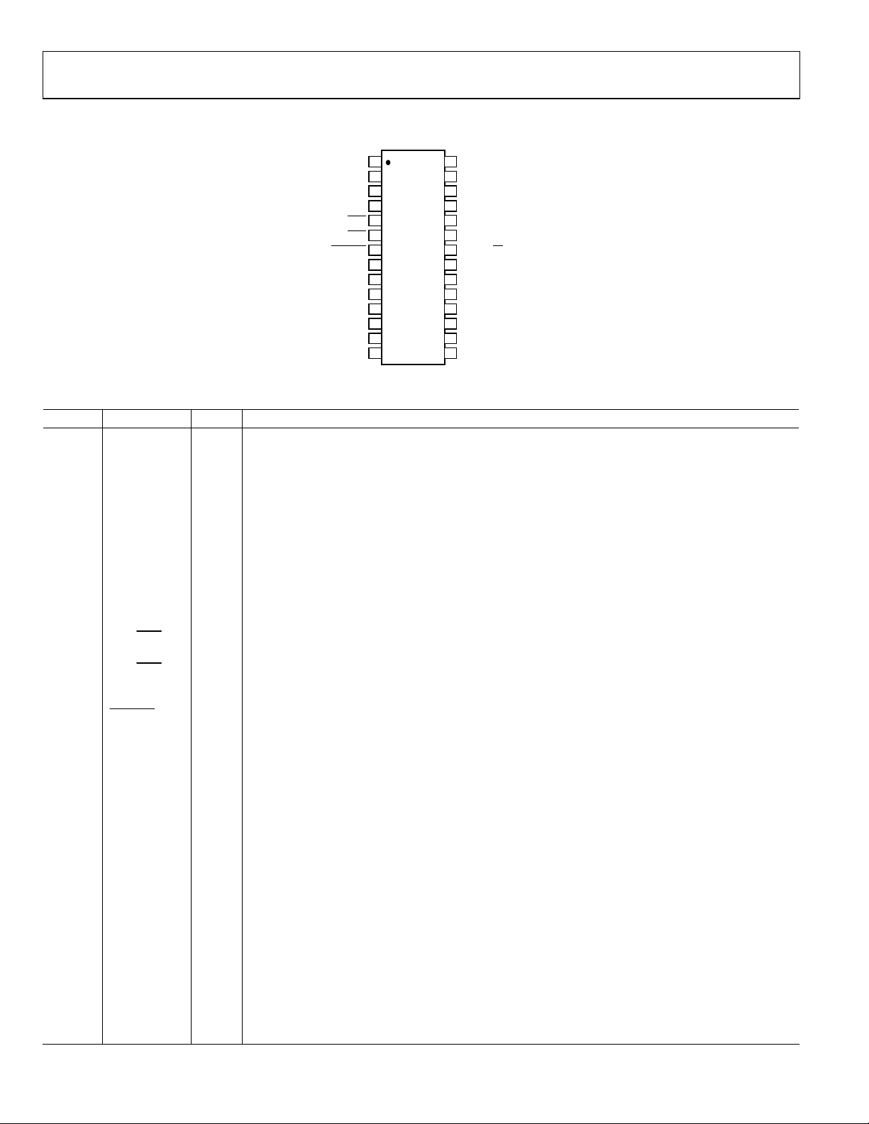
PIN CONFIGURATION AND FUNCTION DESCRIPTION
DGND
1
DLOAD
2
P3.0/RxD
P3.1/TxD
P3.2/INT0
P3.3/INT1
P3.4/T0/CONVST
P1.1/T2EX
P1.2/ADC0
P1.3/ADC1
P1.0/T2
RESET
AV
AGND
DD
3
4
5
6
ADuC814
7
TOP VIEW
8
(Not to Scale)
9
10
11
12
13
14
Figure 2. Pin Configuration
Table 3. Pin Descriptions
Pin No. Mnemonic Type Function
1 DGND S Digital Ground. Ground reference point for the digital circuitry.
2 DLOAD I
Debug/Serial Download Mode. Enables when pulled high through a resistor on power-on or RESET. In
this mode, DLOAD may also be used as an external emulation I/O pin, therefore the voltage level at
this pin must not be changed during this mode of operation because it may cause an emulation
interrupt that halts code execution. User code is executed when this pin is pulled low on power-on or
RESET.
3–7 P3.0 – P3.4 I/O
Bidirectional Port Pins with Internal Pull-Up Resistors. Port 3 pins that have 1s written to them are
pulled high by the internal pull-up resistors, and in that state they can be used as inputs. As inputs,
with Port 3 pins being pulled low externally, they source current because of the internal pull-up
resistors. When driving a 0-to-1 output transition, a strong pull-up is active during S1 of the
instruction cycle. Port 3 pins also have various secondary functions which are described next.
3 P3.0/RxD I/O Receiver Data Input (asynchronous) or Data Input/Output (synchronous) in Serial (UART) Mode.
4 P3.1/TxD I/O Transmitter Data Output (asynchronous) or Clock Output (synchronous) in Serial (UART) Mode.
5
P3.2/
INT0
I/O
Interrupt 0, programmable edge or level-triggered interrupt input, which can be programmed to one
of two priority levels. This pin can also be used as agate control input to Timer 0.
6
P3.3/
INT1
I/O
Interrupt 1, programmable edge or level-triggered interrupt input, which can be programmed to one
of two priority levels. This pin can also be used as agate control input to Timer 1.
7
P3.4/T0/
CONVST
8–9 P1.0–P1.1 I/O
I/O Timer/Counter 0 Input and External Trigger Input for ADC Conversion Start.
Bidirectional Port Pins with Internal Pull-Up Resistors. Port 1 pins that have 1s written to them are
pulled high by the internal pull-up resistors, and in that state they can be used as inputs. As inputs
,with Port 1 pins being pulled low externally, they source current because of the internal pull-up
resistors When driving a 0-to-1 output transition a strong pull-up is active during S1 of the instruction
cycle. Port 1 pins also have various secondary functions which are described as follows.
8 P1.0/T2 I/O
Timer 2 Digital Input. Input to Timer/Counter 2. When enabled, Counter 2 is incremented in response
to a 1 to 0 transition of the T2 input.
9 P1.1/T2EX I/O Digital Input. Capture/Reload trigger for Counter 2.
10 RESET I
Reset Input. A high level on this pin while the oscillator is running resets the device. There is an
internal weak pull-down and a Schmitt-trigger input stage on this pin.
11–12 P1.2–P1.3 I
Port 1.2 to P1.3. These pins have no digital output drivers, i.e., they can only function as digital inputs,
for which 0 must be written to the port bit. These port pins also have the following analog functionality:
11 P1.2/ADC0 I ADC Input Channel 0. Selected via ADCCON2 SFR.
12 P1.3/ADC1 I ADC Input Channel 1. Selected via ADCCON2 SFR.
13 AVDD S Analog Positive Supply Voltage, 3 V or 5 V.
14–15 AGND G Analog Ground. Ground reference point for the analog circuitry.
16 V
I/O
REF
Reference Input/Output. This pin is connected to the internal reference through a switch and is the
reference source for the analog to digital converter. The nominal internal reference voltage is 2.5 V
and this appears at the pin. This pin can be used to connect an external reference to the analog to
digital converter by setting ADCCON1.6 to 1. Connect 0.1 µF between this pin and AGND.
DV
28
DD
XTAL2
27
26
XTAL1
25
SCLOCK
24
P3.7/SDATA/MOSI
P3.6/MISO
23
22
P3.5/T1/SS/EXTCLK
21
P1.7/ADC5/DAC1
20
P1.6/ADC4/DAC0
P1.5/ADC3
19
P1.4/ADC2
18
17
C
REF
V
16
REF
AGND
15
02748-A-009
Rev. A | Page 10 of 72

ADuC814
Pin No. Mnemonic Type Function
17 C
18–21 P1.4–P1.7 I
18 P1.4/ADC2 I ADC Input Channel 2. Selected via ADCCON2 SFR.
19 P1.5/ADC3 I ADC Input Channel 2. Selected via ADCCON2 SFR.
20
21
22–24 P3.5–P3.7 I/O
22 P3.5/T1
22
23 P3.6/MISO I/O SPI Master Input/Slave Output Data Input/Output Pin.
24
25 SCLOCK I/O Serial Clock Pin for SPI Serial Interface Clock.
26 XTAL1 I Input to the Crystal Oscillator Inverter.
27 XTAL2 O Output from the Crystal Oscillator Inverter.
28 DVDD S Analog Positive Supply Voltage, 3 V or 5 V.
I = Input, O = Output, S = Supply, G - Ground.
I Decoupling Input for On-Chip Reference. Connect 0.1 µF between this pin and AGND.
REF
Port 1.4 to P1.7. These pins have no digital output drivers, i.e., they can only function as digital inputs,
for which 0 must be written to the port bit. These port pins also have the following analog functionality:
P1.6/ADC4/
DAC0
P1.7/
ADC5/DAC1
SS
P3.5/
/EXTCLK
P3.7/SDATA/
MOSI
I/O
I/O
I/O
I/O SPI Master Output/Slave Input Data Input/Output Pin.
ADC Input Channel 4. Selected via ADCCON2 SFR. The voltage DAC Channel 0 can also be configured
to appear on P1.6.
ADC Input Channel 5, selected via ADCCON2 SFR. The voltage DAC Channel 1 can also be configured
to appear on P1.7.
Bidirectional Port Pins with Internal Pull-Up Resistors. Port 3 pins that have 1s written to them are
pulled high by the internal pull-up resistors, and in that state they can be used as inputs. As inputs
,with Port 3 pins being pulled low externally, they source current because of the internal pull-up
resistors. When driving a 0-to-1 output transition a strong pull-up is active during S1 of the instruction
cycle. Port 3 pins also have various secondary functions which are described as follows.
I/O Timer/Counter 1 Input. P3.5–P3.7 pins also have SPI interface functions. To enable these functions,
Bit 0 of the CFG814 SFR must be set to 1.
This pin also functions as the Slave Select input for the SPI interface when the device is operated in
slave mode. P3.5 can also function as an input for an external clock. This clock effectively bypasses the
PLL. This function is enabled by setting Bit 1 of the CFG814 SFR.
The following notes apply to the entire data sheet:
• In bit designation tables, set implies a Logic 1 state, and cleared implies a Logic 0 state, unless otherwise stated.
• Set and cleared also imply that the bit is set or cleared by the ADuC814 hardware, unless otherwise stated.
• User software should not write to reserved or unimplemented bits as they may be used in future products.
Rev. A | Page 11 of 72

ADuC814
TERMINOLOGY
ADC SPECIFICATIONS
Integral Nonlinearity
This is the maximum deviation of any code from a straight line
passing through the endpoints of the ADC transfer function.
The endpoints of the transfer function are zero scale, a
point1/2 LSB below the first code transition and full scale, a
point 1/2 LSB above the last code transition.
Differential Nonlinearity
This is the difference between the measured and the ideal 1 LSB
change between any two adjacent codes in the ADC.
Offset Error
This is the deviation of the first code transition (0000 … 000) to
(0000 … 001) from the ideal, i.e., +1/2 LSB.
DAC SPECIFICATIONS
Relative Accuracy
Relative accuracy or endpoint linearity is a measure of the
maximum deviation from a straight line passing through the
endpoints of the DAC transfer function. It is measured after
adjusting for zero-scale error and full-scale error.
Voltage Output Settling Time
This is the amount of time it takes for the output to settle to a
specified level for a full-scale input change.
Digital-to-Analog Glitch Impulse
This is the amount of charge injected into the analog output
when the inputs change state. It is specified as the area of the
glitch in nV-sec.
Full-Scale Error
This is the deviation of the last code transition from the ideal
AIN voltage (full-scale error has been adjusted out).
Signal-to-(Noise + Distortion) Ratio
This is the measured ratio of signal-to-(noise + distortion) at
the output of the ADC. The signal is the rms amplitude of the
fundamental. Noise is the rms sum of all nonfundamental
signals up to half the sampling frequency (f
The ratio is dependent upon the number of quantization levels
in the digitization process; the more levels, the smaller the
quantization noise. The theoretical signal-to-(noise + distortion)
ratio for an ideal N-bit converter with a sine wave input is given
by
Signal-to =- (Noise + Distortion) = (6.02N + 1.76)
Thus, for a 12-bit converter, this is 74 dB.
Total Harmonic Distortion (THD)
Total harmonic distortion is the ratio of the rms sum of the
harmonics to the fundamental.
Peak Harmonic or Spurious Noise
Peak harmonic or spurious noise is defined as the ratio of the
rms value of the next largest component in the ADC output
spectrum (up to f
fundamental. Normally, the value of this specification is
determined by the largest harmonic in the spectrum, but for
ADCs where the harmonics are buried in the noise floor, it is
the noise peak.
/2 and including dc) to the rms value of the
S
/2), excluding dc.
S
Rev. A | Page 12 of 72
ADuC814
TYPICAL PERFORMANCE CURVES
The typical performance plots presented in this section
illustrate typical performance of the ADuC814 under various
operating conditions. Note that all typical plots in this section
were generated using the ADuC814BRU, i.e., the B-grade part.
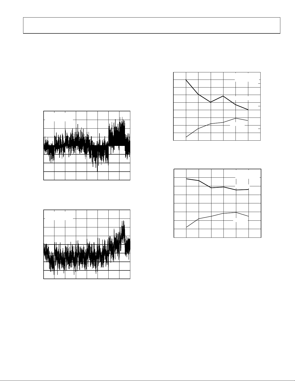
Figure 3 and Figure 4 show typical ADC integral nonlinearity
(INL) errors from ADC Code 0 to Code 4095 at 5 V and 3 V
supplies, respectively. The ADC is using its internal reference
(2.5 V) and operating at a sampling rate of 152 kHz. The typical
worst-case errors in both plots are just less than 0.3 LSBs.
0.4
AVDD/DVDD = 5V
f
= 152kHz
S
0.3
0.2
0.1
0
LSBs
–0.1
–0.2
–0.3
–0.4
LSBs
–0.1
–0.2
–0.3
–0.4
0
0.4
AVDD/DVDD = 3V
f
0.3
0.2
0.1
0
0
1023511 35833071255920471535 4095
Figure 3. Typical I NL Error, V
ADC CODES
DD
= 5 V
= 152kHz
S
1023511 35833071255920471535 4095
Figure 4. Typical I NL Error, V
ADC CODES
DD
= 3 V
02748-A-010
02748-A-011
Figure 5 and Figure 6 show the variation in worst-case positive
(WCP) INL and worst-case negative (WCN) INL versus
external reference input voltage.
1.2
1.0
0.8
0.6
0.4
0.2
WCP–INL (LSBs)
0
–0.2
–0.4
–0.6
0.5 1.0 1.5 2.0 2.5 5.0
EXTERNAL REFERENCE (V)
Figure 5. Typical Worst-Case INL Error vs. V
0.8
0.6
0.4
0.2
0
–0.2
WCP–INL (LSBs)
–0.4
–0.6
–0.8
0.5 1.5 2.5
EXTERNAL REFERENCE (V)
Figure 6. Typical Worst-Case INL Error vs. V
AVDD/DVDD = 5V
f
= 152kHz
S
WCP INL
WCN INL
, VDD = 5 V
REF
AVDD/DVDD = 3V
f
= 152kHz
S
WCP INL
WCN INL
3.02.01.0
, VDD = 3 V
REF
0.6
0.4
0.2
0
–0.2
–0.4
–0.6
0.8
0.6
0.4
0.2
0
–0.2
–0.4
–0.6
–0.8
WCN–INL (LSBs)
02748-A-012
WCN–INL (LSBs)
02748-A-013
Figure 7 and Figure 8 show typical ADC differential nonlinearity
(DNL) errors from ADC Code 0 to Code 4095 at 5 V and 3 V
supplies, respectively. The ADC is using its internal reference
(2.5 V) and operating at a sampling rate of 152 kHz. The typical
worst-case errors in both plots are just less than 0.2 LSBs.
Rev. A | Page 13 of 72
ADuC814
0.30
0.25
0.20
0.15
0.10
0.05
0
LSBs
–0.50
–0.10
–0.15
AVDD/DVDD = 5V
–0.20
f
= 152kHz
S
–0.25
0
1023511 35833071255920471535 4095
Figure 7. Typical DNL Error, V
ADC CODES
DD
= 5 V
02748-A-014
0.30
AVDD/DVDD = 3V
0.25
f
= 152kHz
S
0.20
0.15
0.10
0.05
0
LSBs
–0.50
–0.10
–0.15
–0.20
–0.25
0
1023511 35833071255920471535 4095
Figure 8. Typical DNL Error, V
ADC CODES
DD
= 3 V
02748-A-015
Figure 9 and Figure 10 show the variation in worst-case positive
(WCP) DNL and worst-case negative (WCN) DNL versus
external reference input voltage.
0.6
0.4
0.2
0
WCP–DNL (LSBs)
–0.2
–0.4
–0.6
0.5
1.0 2.0 2.5 5.0
1.5
EXTERNAL REFERENCE (V)
Figure 9. Typical Worst-Case DNL Error vs. V
AVDD /DVDD = 5V
f
= 152kHz
S
WCP DNL
WCN DNL
, VDD = 5 V
REF
0.6
0.4
0.2
0
–0.2
–0.4
–0.6
WCN–DNL (LSBs)
02748-A-016
0.7
0.5
0.3
0.1
–0.1
WCP–DNL (LSBs)
–0.3
–0.5
–0.7
0.5 1.0 1.5 2.0 2.5 3.0
EXTERNAL REFERENCE (V)
Figure 10. Typical Worst-Case DNL Error vs. V
AVDD/DVDD= 3V
f
= 152kHz
S
WCP DNL
WCN DNL
, VDD = 3 V
REF
0.7
0.5
0.3
0.1
–0.1
–0.3
–0.5
–0.7
WCN–DNL (LSBs)
02748-A-017
Figure 11 shows a histogram plot of 10,000 ADC conversion
results on a dc input with V
= 5 V. The plot illustrates an
DD
excellent code distribution pointing to the low noise
performance of the on-chip precision ADC.
10000
8000
6000
4000
OCCURRENCE
2000
0
817 818 819 820 821
Figure 11. Code Histogram plot, V
CODE
DD
= 5 V
02748-A-018
Figure 12 shows a histogram plot of 10,000 ADC conversion
results on a dc input for V
= 3 V. The plot again illustrates a
DD
very tight code distribution of 1 LSB with the majority of codes
appearing in one output bin.
10000
9000
8000
7000
6000
5000
4000
OCCURRENCE
3000
2000
1000
0
817 818 819 820 821
CODE
Figure 12. Code Histogram Plot, V
DD
= 3 V
02748-A-019
Rev. A | Page 14 of 72
ADuC814
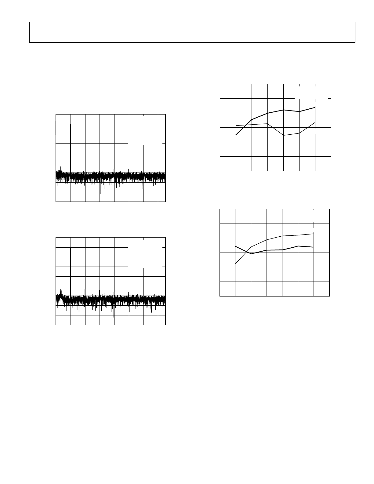
Figure 13 and Figure 14 show typical FFT plots for the ADuC814.
These plots were generated using an external clock input via
P3.5 to achieve coherent sampling. The ADC is using its internal
reference (2.5 V) sampling a full-scale, 10 kHz sine wave test
tone input at a sampling rate of 149.79 kHz. The resultant FFTs
shown at 5 V and 3 V supplies illustrate an excellent 100 dB
noise floor, a 71 dB signal-to-noise ratio (SNR), and a THD
greater than −80 dB.
20
0
–20
–40
–60
dBs
–80
–100
–120
–140
–160
20
1007060504030
FREQUENCY (kHz)
Figure 13. ADuC814 Dynamic Performance at V
20
0
–20
–40
–60
dBs
–80
–100
–120
–140
–160
20
1007060504030
FREQUENCY (kHz)
Figure 14. ADuC814 Dynamic Performance at V
AVDD/DVDD = 5V
f
= 149.79kHz
S
= 9.910kHz
f
IN
SNR = 71.3dB
THD = –88.0dB
ENOB = 11.6
= 5 V
DD
AVDD/DVDD = 3V
= 149.79kHz
f
S
= 9.910kHz
f
IN
SNR = 71.3dB
THD = –88.0dB
ENOB = 11.6
= 3 V
DD
02748-A-020
02748-A-021
Figure 15 and Figure 16 show typical dynamic performance
versus external reference voltages. Again excellent ac performance
can be observed in both plots with some roll-off being observed
as V
falls below 1 V.
REF
THD
–70
–75
–80
–85
–90
–95
–100
–70
–75
–80
–85
–90
–95
–100
THD (dBs)
THD (dBs)
02748-A-023
80
75
70
65
SNR (dBs)
60
55
50
0.5
1.0 2.0 2.5 5.0
1.5
EXTERNAL REFERENCE (V)
Figure 15. Typical Dynamic Performance vs. V
80
75
70
65
SNR (dBs)
60
55
50
0.5 1.5 2.5
1.0 2.0 3.0
EXTERNAL REFERENCE (V)
Figure 16. Typical Dynamic Performance vs. V
AVDD/DVDD = 5V
f
= 152kHz
S
SNR
THD
, VDD = 5 V
REF
AVDD/DVDD = 3V
f
= 152kHz
S
SNR
, VDD = 3 V
REF
02748-A-022
Rev. A | Page 15 of 72
ADuC814
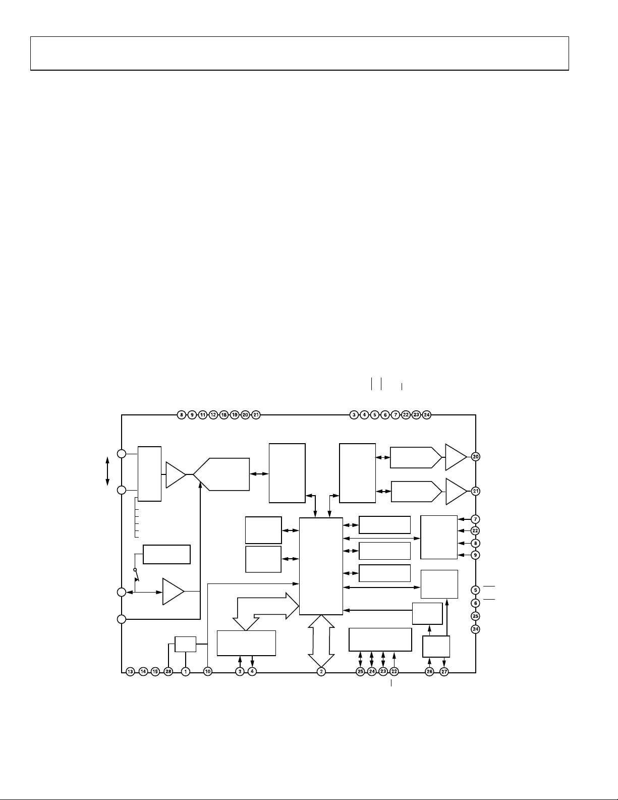
ADuC814 ARCHITECTURE, MAIN FEATURES
The ADuC814 is a fully integrated 247 kSPS 12-bit data
acquisition system incorporating a high performance multichannel ADC, an 8-bit MCU, and program/data Flash/EE
memory on a single chip.
This low power device operates from a 32 kHz crystal with an
on-chip PLL generating a high frequency clock of 16.78 MHz.
This clock is, in turn, routed through a programmable clock
divider from which the MCU core clock operating frequency is
generated.
The microcontroller core is an 8052, and therefore 8051,
instruction set compatible. The microcontroller core machine
cycle consists of 12 core clock periods of the selected core
operating frequency. Eight kbytes of nonvolatile Flash/EE
program memory are provided on-chip. 640 bytes of nonvolatile
Flash/EE data memory and 256 bytes RAM are also integrated
on-chip.
The ADuC814 also incorporates additional analog functionality
with dual 12-bit DACs, a power supply monitor, and a band gap
)
)
0
1
C
C
A
A
D
)
)
)
X
)
E
2
2
T
T
(
(
0
1
.
.
1
1
P
P
)
1
0
2
N
N
N
I
I
I
A
A
A
(
(
(
3
2
4
.
.
.
1
1
1
P
P
P
D
)
/
/
3
4
5
N
N
N
I
I
I
A
A
A
(
(
(
5
6
7
.
.
.
1
1
1
P
P
P
reference. On-chip digital peripherals include a watchdog timer,
time interval counter, three timer/counters, and three serial I/O
2
ports (SPI, UART, I
C).
On-chip factory firmware supports in-circuit serial download
and debug modes (via UART), as well as single-pin emulation
mode via the DLOAD pin. A detailed functional block diagram
of the ADuC814 is shown in Figure 17.
The ADuC814 is supported by a QuickStart
Development
System. This is a full-featured, low cost system, consisting of
PC-based (Windows compatible) hardware and software
development tools.
The part operates from a single 3 V or 5 V supply. When
operating from 3 V supplies, the power dissipation for the part
is below 10 mW. The ADuC814 is housed in a 28-lead TSSOP
package and is specified for operation over an extended
temperature range −40°C to +125°C.
)
K
L
)
C
1
T
D
)
/
X
)
)
)
)
1
0
D
D
X
X
T
R
(
(
0
1
.
.
3
3
P
P
)
T
T
0
N
N
I
I
T
(
(
(
3
2
4
.
.
.
3
3
3
P
P
P
I
O
E
S
/
S
I
O
S
S
M
M
(
(
(
5
6
7
.
.
.
3
3
3
P
P
P
ADC0
ADC5
V
REF
C
REF
11
21
16
17
DD
AV
AIN
T/H
MUX
TEMP MONITOR
DAC0
DAC1
V
REF
AGND
BAND GAP
REFERENCE
BUF
DD
DV
AGND
AGND
POR
ADuC814
DAC0
DAC1
T0
T1
T2
T2EX
INT0
INT1
D0
D1
02748-A-024
256 × 8
TIMER
MISO
SS
DAC0
DAC1
PROG.
CLOCK
DIVIDER
ADC
12-BIT
ADC
DOWNLOADER
ASYNCHRONOUS
SERIAL PORT
(UART)
D
N
G
D
RESET
RxD
CONTROL
640 × 8
DATA
FLASH/EE
8k × 8
PROGRAM
FLASH/EE
DEBUGGER
TxD
AND
CAL
LOGIC
8052
MCU
CORE
SINGLE-PIN
EMULATOR
DLOAD
DAC
CONTROL
LOGIC
POWER SUPPLY
SPI SERIAL
INTERFACE
0
D
/
K
C
O
L
C
S
USER RAM
WATCHDOG
MONITOR
1
D
/
I
S
O
M
16-BIT
COUNTER
TIMERS
TIME
INTERVAL
COUNTER
OSC
AND
PLL
XTAL1
XTAL2
BUF
BUF
Figure 17. ADuC814 Block Diagram
Rev. A | Page 16 of 72
ADuC814
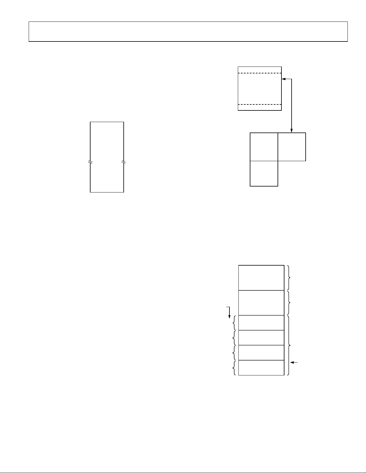
MEMORY ORGANIZATION
The ADuC814 does not have Port 0 and Port 2 pins and
therefore does not support external program or data memory
interfaces. The device executes code from the internal 8-kByte
Flash/EE program memory. This internal code space can be
programmed via the UART serial port interface while the device
is in-circuit. The program memory space of the ADuC814 is
shown in Figure 18.
PROGRAM MEMORY SPACE
READ-ONLY
1FFFH
INTERNAL
8 kBYTE
FLASH/EE
PROGRAM
MEMORY
0000H
02748-A-025
Figure 18. Program Memory Map
The data memory address space consists of internal memory
only. The internal memory space is divided into four physically
separate and distinct blocks, namely the lower 128 bytes of
RAM, the upper 128 bytes of RAM, the 128 bytes of special
function register (SFR) area, and a 640-byte Flash/EE data
memory. While the upper 128 bytes of RAM and the SFR area
share the same address locations, they are accessed through
different addressing modes.
The lower 128 bytes of data memory can be accessed through
direct or indirect addressing, the upper 128 bytes of RAM can
be accessed through indirect addressing, and the SFR area is
accessed through direct addressing.
Also, as shown in Figure 19, an additional 640 bytes of Flash/EE
data memory are available to the user and can be accessed
indirectly via a group of control registers mapped into the SFR
area. Access to the Flash/EE data memory is discussed in detail
later as part of the Flash/EE Memory section.
9FH
00H
UPPER
128
LOWER
128
The lower 128 bytes of internal data memory are mapped as
shown in Figure 20. The lowest 32 bytes are grouped into four
banks of eight registers addressed as R0 to R7. The next 16 bytes
(128 bits), locations 20H to 2FH above the register banks, form
a block of directly addressable bit locations at bit addresses 00H
through 7FH. The stack can be located anywhere in the internal
memory address space, and the stack depth can be expanded up
to 256 bytes.
BANKS
SELECTED
VIA
BITS IN PSW
11
10
01
00
Figure 20. Lower 128 Bytes of Internal Data Memory
DATA MEMORY SPACE
READ/WRITE
(PAGE 159)
640 BYTES
FLASH/EE DATA
MEMORY
ACCESSED
INDIRECTLY
VIA SFR
CONTROL REGISTERS
(PAGE 0)
INTERNAL
DATA MEMORY
SPACE
FFH
80H
7FH
AND INDIRECT
00H
ACCESSIBLE
BY
INDIRECT
ADDRESSING
ONLY
ACCESSIBLE
BY
DIRECT
ADDRESSING
SPECIAL
FUNCTION
REGISTERS
ACCESSIBLE
BY DIRECT
ADDRESSING
ONLY
Figure 19. Data Memory Map
7FH
30H
2FH
20H
18H
10H
08H
00H
1FH
17H
0FH
07H
FFH
80H
02748-A-026
GENERAL-PURPOSE
AREA
BIT-ADDRESSABLE
BIT ADDRESSES
FOUR BANKS OF EIGHT
REGISTERS
R0 R7
RESET VALUE OF
STACK POINTER
02748-A-027
RESET initializes the stack pointer to location 07H and increments it once to start from location 08H, which is also the first
register (R0) of Register Bank 1. If more than one register bank
is being used, the stack pointer should be initialized to an area
of RAM not used for data storage.
Rev. A | Page 17 of 72
ADuC814
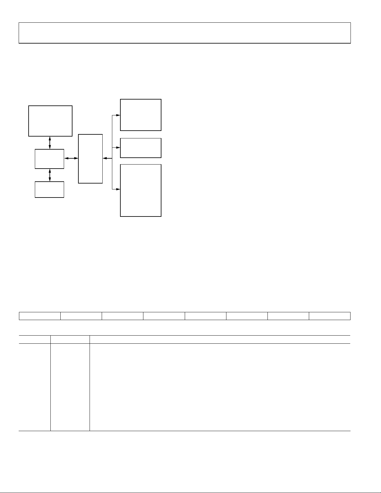
The SFR space is mapped to the upper 128 bytes of internal
data memory space and is accessed by direct addressing only. It
provides an interface between the CPU and all on-chip peripherals. A block diagram showing the programming model of the
ADuC814 via the SFR area is shown in Figure 21. A complete
SFR map is shown in Figure 22.
640-BYTE
8-kBYTE
ELECTRICALLY
REPROGRAMMABLE
NONVOLATILE
FLASH/EE PROGRAM
MEMORY
8051
COMPATIBLE
CORE
256 BYTES
RAM
128-BYTE
SPECIAL
FUNCTION
REGISTER
AREA
Figure 21. Programming Model
ELECTRICALLY
REPROGRAMMABLE
NONVOLATILE
FLASH/EE DATA
MEMORY
6-CHANNEL
12-BIT SAR ADC
OTHER ON-CHIP
PERIPHERALS
TEMPERATURE
MONITOR
DUAL 12-BIT DAC
SERIAL I/O
WDT
PSM
TIC
PLL
02748-A-028
Program Status Word SFR
The program status word (PSW) register is the program status word that contains several bits reflecting the current status of the CPU as
detailed in Table 4.
OVERVIEW OF MCU-RELATED SFRS
Accumulator SFR
ACC is the accumulator register and is used for math operations
including addition, subtraction, integer multiplication and
division, and Boolean bit manipulations. The mnemonics for
accumulator-specific instructions refer to the accumulator as A.
B SFR
The B register is used with the ACC for multiplication and
division operations. For other instructions it can be treated as a
general-purpose scratchpad register.
Stack Pointer SFR
The SP register is the stack pointer and is used to hold an internal
RAM address called the top of the stack. The SP register is
incremented before data is stored during PUSH and CALL
executions. While the stack may reside anywhere in on-chip
RAM, the SP register is initialized to 07H after a reset. This
causes the stack to begin at location 08H.
Data Pointer
The data pointer is made up of two 8-bit registers, named DPH
(high byte) and DPL (low byte). These registers provide memory
addresses for internal code access. The pointer may be manipulated as a 16-bit register (DPTR = DPH, DPL), or as two independent 8-bit registers (DPH, DPL).
SFR Address D0H
Power-On Default 00H
Bit Addressable Yes
CY AC F0 RS1 RS0 OV F1 P
Table 4. PSW SFR Bit Designations
Bit No. Name Description
7 CY Carry Flag.
6 AC Auxiliary Carry Flag.
5 F0 General-Purpose Flag.
4 RS1 Register Bank Select Bits.
3 RS0 RS1 RS0 Selected Bank
0 0 0
0 1 1
1 0 2
1 1 3
2 OV Overflow Flag.
1 F1 General-Purpose Flag.
0 P Parity Bit.
Rev. A | Page 18 of 72
ADuC814
Power Control SFR
The power control (PCON) register contains bits for power-saving options and general-purpose status flags as shown in Table 5.
SFR Address 87H
Power-On Default 00H
Bit Addressable No
SMOD SERIPD INT0PD --- GF1 GF0 PD IDL
Table 5. PCON SFR Bit Designations
Bit No. Name Description
7 SMOD Double UART Baud Rate.
6 SERIPD SPI Power-Down Interrupt Enable.
5 INT0PD
4 RSVD Reserved.
3 GF1 General-Purpose Flag Bit.
2 GF0 General-Purpose Flag Bit.
1 PD Power-Down Mode Enable.
0 IDL Idle Mode Enable.
Power-Down Interrupt Enable.
INT0
Rev. A | Page 19 of 72
ADuC814
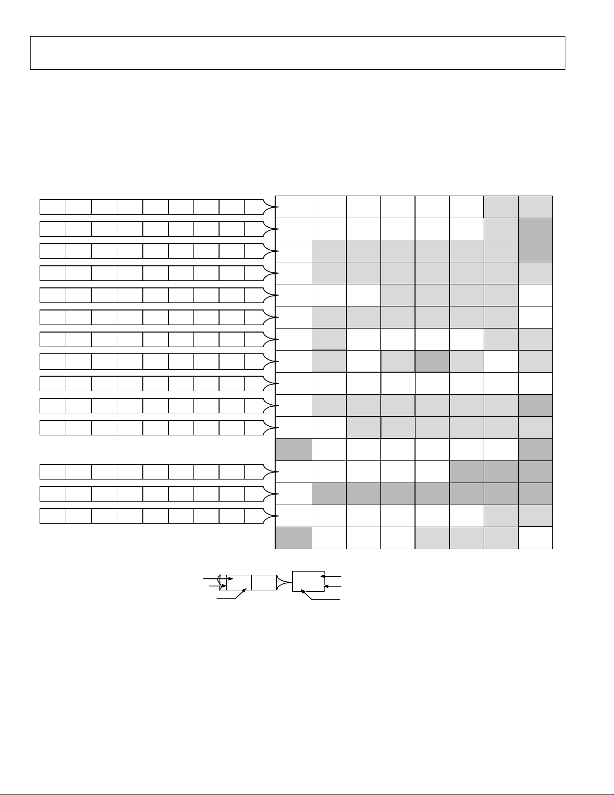
SPECIAL FUNCTION REGISTERS
All registers, except the program counter and the four generalpurpose register banks, reside in the SFR area. The SFR registers
include control, configuration, and data registers that provide an
interface between the CPU and all on-chip peripherals.
Figure 22 shows a full SFR memory map and SFR contents on
RESET; NOT USED indicates unoccupied SFR locations.
ISPI
WCOL
SPE
SPIM
CPOL
CPHA
FFH
0
FEH 0
FDH 0
FCH 0
FBH 0
F7H 0 F6H 0 F5H 0 F4H 0 F3H 0 F2H F1H 0 F0H 0
D1EN D0EN
D1
EFH
0
EEH 0D0EDH 0 ECH 0 EBH 0 EAH E9H 0 E8H 0
E7H 0 E6H 0 E5H 0 E4H 0 E3H 0 E2H E1H 0 E0H 0
ADCI
ADCSPI
CCONV
DFH
0
DEH 0
CY
D7H 0ACD6H 0F0D5H 0
TF2
EXF2
CFH 0
CEH 0
PRE3
PRE2
C7H 0
C6H 0
PSI
PADC
BFH 0
BEH 0
RD
B7H 1WRB6H 1T1B5H 1T0B4H 1
EA
EADC
AFH
AEH
00
0
SM0
TF1
SM1
9EH 0
TR1
8EH 0
9FH 0
97H 1 96H 1 95H 1 94H 1 93H 1 92H
8FH 0
SCONV
DDH 0
DCH 0
D4H 0
RCLK
CDH 0
CCH 0
PRE1
C5H 0 C4H 1
PT2
BDH 0PSBCH 0
ET2
ADHESACH 0
SM2
9DH 0
9CH 0
TF0
8DH 0
8CH 0
CS3
DBH 0
RS1
RS0
D3H 0OVD2HFID1H 0PD0H 0
TCLK
EXEN2
CBH 0
WDIR
PRE0
C3H 0
PT1
BBH 0
INT1
B3H 1
ET1
ABH 0
REN
TB8
9BH 0
TR0
IE1
8BH 0
SPR1
FAH
F9H 0
1
0
0
0
CS2
CS1
0
DAH
D9H 0
0
TR2
CNT2
0
CAH
C9H 0
WDS
0
C2HWDC1H 0
PX1
PT0
BAH
B9H 0
0
INT0
TxD
B2H
B1H 1
1
EX1
ET0
AAH
A9H 0
0
RB8
0
9AHTI99H 0RI98H 0
T2EX
1
91H 1T290H 1
IT1
IE0
0
8AH
89H 0
SPR0
F8H
CS0
D8H
CAP2
C8H 0
WDWR
C0H 0
PX0
B8H 0
RxD
B0H 1
EX0
A8H 0
IT0
88H 0
5
BITS
0
BITS
BITS
BITS
BITS
0
BITS
BITS
BITS
BITS
BITS
BITS
BITS
BITS
BITS
Unoccupied locations in the SFR address space are not
implemented, i.e., no register exists at this location. If an
unoccupied location is read, an unspecified value is returned.
SFR locations reserved for future use are shaded (RESERVED)
and should not be accessed by the user software.
1
SPICON
F8H
F0H 00H
DCON
E8H 00H
ACC
E0H 00H
ADCCON2
D8H 00H
PSW
D0H 00H
T2CON
C8H 00H
WDCON
C0H 10H
B8H 00H
B0H FFH
A8H 00H
NOT USED NOT USED
SCON
98H 00H
P1
90H FFH
TCON
88H 00H
NOT USED
IP
P3
IE
B
1,2
04H
1
1
1
1
1
1
1
1
1
1
DAC0L
F9H 00H
ADCOFSL
F1H 00H
1
ADCDATAL
D9H 00H
RESERVED
1
RESERVED
ECON
B9H 00H
IEIP2
A9H A0H
TIMECON
A1H
SBUF
99H 00H
TMOD
89H 00H
81H 07H
DAC0H
FAH 00H
ADCOFSH
F2H 20H
ADCDA T AH
DAH 00H
RCAP2L
CAH 00H
CHIPID
C2H 0XH
ETIM1
BAH 00H
RESERVEDRESERVED RESERVED
RESERVED RESERVED
HTHSEC
A2H A3H A4H
00H 00H 00H 00H
I2CDAT
9AH 00H
TL0
8AH 00H
SP
DPL
82H 00H
DAC1L
FBH 00H
ADCGAINL
F3H 00H
RESERVEDRESERVED
RCAP2H
CBH 00H
RESERVED
ETIM2
BBH 00H
SEC
I2CADD
9BH 55H
TL1
8BH 00H
DPH
83H 00H
DAC1H
FCH 00H
ADCGAINH
F4H 00H
CCH 00H
NOT USED
EDATA1
BCH 00H
RESERVED RESERVED
RESERVED RESERVED
TL2
MIN
DACCON
FDH 04H
ADCCON3
F5H 00H
RESERVEDRESERVEDRESERVEDRESERVEDRESERVED
RESERVEDRESERVEDRESERVEDRESERVEDRESERVED
RESERVEDRESERVEDRESERVED
RESERVEDRESERVEDRESERVED
TH2
CDH 00H
RESERVED
EDATA2
BDH 00H
HOUR IN TV A L
A5H
00H 00H
CFG814
9CH 04H
NOT USEDNOT USEDNOT USEDNOT USEDNOT USED
TH0
8CH 00H
RESERVED
TH1
8DH 00H
RESERVED
RESERVED
RESERVED
RESERVED
RESERVED
RESERVED
RESERVED
EDARL
C6H 00H
EDATA3
BEH 00H
RESERVED
RESERVED
A6H
NOT USED
NOT USED
RESERVED RESERVED
RESERVEDRESERVED
RESERVED
SPIDAT
F7H 00H
ADCCON1
EFH 00H
RESERVED
PSMCON
DFH DEH
PLLCON
D7H 53H
RESERVED
RESERVED
EDATA4
BFH 00H
NOT USED
RESERVED
NOT USEDNOT USED
NOT USED
PCON
87H 00H
SFR MAP KEY:
MNEMONIC
SFR ADDRESS
DEFAULT VALUE
THESE BITS ARE CONTAINED IN THIS BYTE.
IE0
89H 0
IT0
88H 0
TCON
88H 00H
MNEMONIC
DEFAULT VALUE
SFR ADDRESS
Figure 22. Special Function Register Locations and Reset Values
Note the following about SFRs:
• SFRs whose address ends in 0H or 8H are bit addressable.
• Only P1.0 and P1.1 can operate as digital I/O pins. P1.2–P1.7 can be configured as analog inputs (ADC inputs) or as digital inputs.
• The CHIPID SFR contains the silicon revision ID byte and may change for future silicon revisions.
• These registers are reconfigured at power-on with factory calculated calibration coefficients that can be overwritten by user code. See
the calibration options in ADCCON3 SFR.
SS
• When the SPIM bit in the SPICON SFR is cleared, the SPR0 bit reflects the level on the
Rev. A | Page 20 of 72
pin (Pin 22).
02748-0-029
ADuC814
ADC CIRCUIT INFORMATION
GENERAL OVERVIEW
The ADC block incorporates a 4.05 msec, 6-channel, 12-bit
resolution, single-supply ADC. This block provides the user
with a multichannel multiplexer, track-and-hold amplifier, onchip reference, offset calibration features and ADC. All components in this block are easily configured via a 3-register SFR
interface.
The ADC consists of a conventional successive-approximation
converter based around a capacitor DAC. The converter accepts
an analog input range of 0 V to V
brated 2.5 V reference is provided on-chip. An external reference
may also be used via the external V
ence can be in the range 1.0 V to AV
Single or continuous conversion modes can be initiated in
software. In hardware, a convert signal can be applied to an
external pin (CONVST), or alternatively Timer 2 can be configured to generate a repetitive trigger for ADC conversions.
The ADuC814 has a high speed ADC to SPI interface data
capture logic implemented on-chip. Once configured, this logic
transfers the ADC data to the SPI interface without the need for
CPU intervention.
The ADC has six external input channels. Two of the ADC
channels are multiplexed with the DAC outputs, ADC4 with
DAC0, and ADC5 with DAC1. When the DAC outputs are in
use, any ADC conversion on these channels represents the DAC
output voltage. Due care must be taken to ensure that no
external signal is trying to drive these ADC/DAC channels
while the DAC outputs are enabled.
In addition to the six external channels of the ADC, five internal
signals are also routed through the front end multiplexer. These
signals include a temperature monitor, DAC0, DAC1, V
AGND. The temperature monitor is a voltage output from an
on-chip band gap reference, which is proportional to absolute
temperature. These internal channels can be selected similarly
to the external channels via CS3–CS0 bits in the ADCCON2 SFR.
The ADuC814 is shipped with factory programmed offset and
gain calibration coefficients that are automatically downloaded
to the ADC on a power-on or RESET event, ensuring optimum
ADC performance. The ADC core contains automatic endpoint
self-calibration and system calibration options that allow the
user to overwrite the factory programmed coefficients if desired
and tailor the ADC transfer function to the system in which it is
being used.
. A precision, factory cali-
REF
pin. This external refer-
REF
.
DD
REF
, and
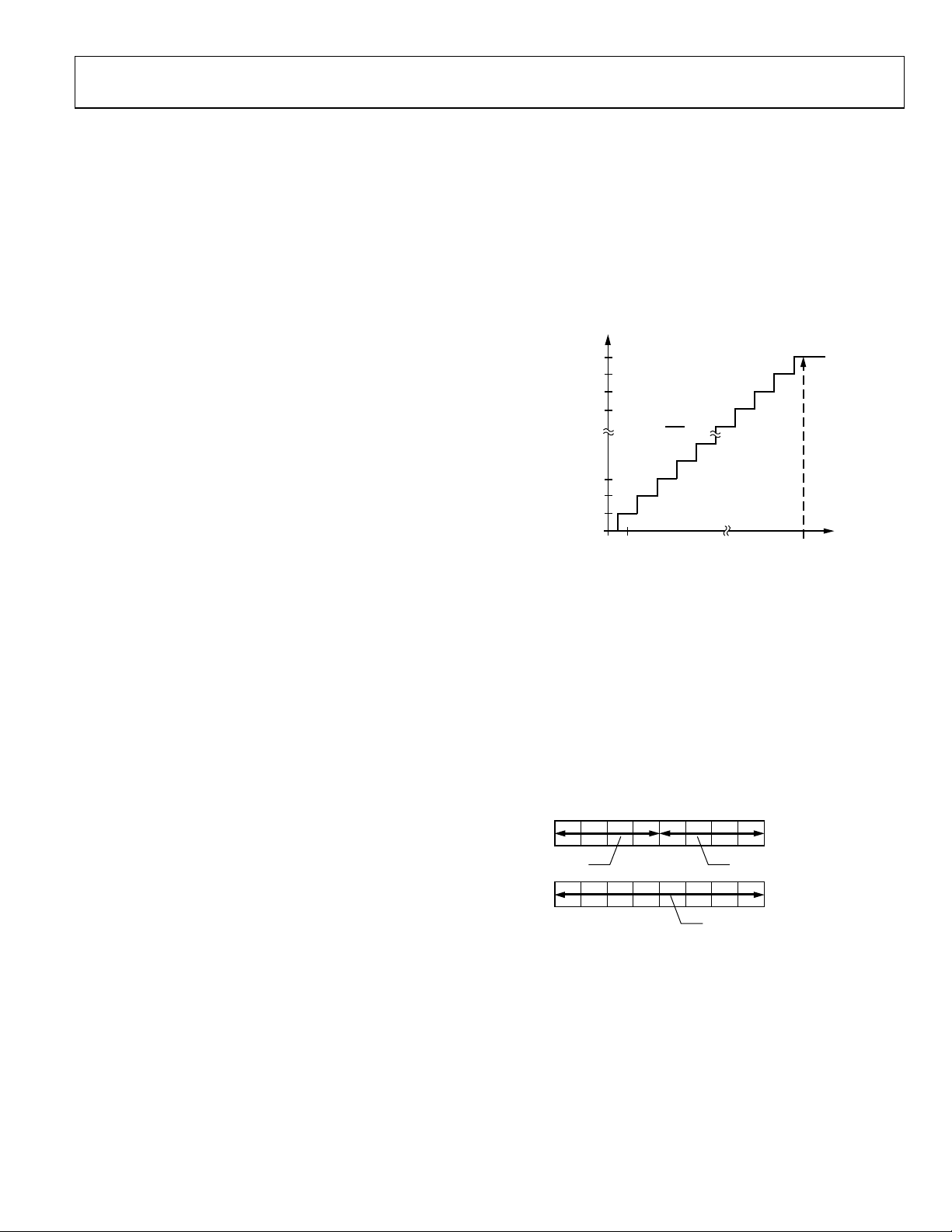
ADC TRANSFER FUNCTION
The analog input range for the ADC is 0 V to V
range, the designed code transitions occur midway between
successive integer LSB values, i.e., 1/2 LSB, 3/2 LSBs, 5/2 LSBs . . .
FS –3/2 LSBs. The output coding is straight binary with 1 LSB =
FS/4096 or 2.5 V/4096 = 0.61 mV when V
REF
input/output transfer characteristic for the 0 V to V
shown in Figure 23.
OUTPUT
CODE
111...111
111...110
111...101
111...100
000...011
000...010
000...001
000...000
0V 1LSB
Figure 23. ADuC814 ADC Transfer Function
1LSB =
FS
4096
VOLTAGE INPUT
ADC Data Output Format
Once configured via the ADCCON1–3 SFRs, the ADC converts
the analog input and provides an ADC 12-bit result word in the
ADCDATAH/L SFRs. The ADCDATAL SFR contains the
bottom 8 bits of the 12-bit result. The bottom nibble of the
ADCDATAH SFR contains the top 4 bits of the result, while the
top nibble contains the channel ID of the ADC channel which
has been converted on. This ID corresponds to the channel
selection bits CD3–CD0 in the ADCCON2 SFR. The format of
the ADC 12-bit result word is shown in Figure 24.
CH–ID
TOP 4 BITS
Figure 24. ADC Result Format
HIGH 4 BITS OF
ADC RESULT WORD
LOW 8 BITS OF THE
ADC RESULT WORD
. For this
REF
= 2.5 V. The ideal
range is
REF
+FS
ADCDATAH SFR
ADCDATAL SFR
02748-A-030
02748-A-031
Rev. A | Page 21 of 72

ADuC814
SFR INTERFACE TO ADC BLOCK
The ADC operation is fully controlled via three SFRs: ADCCON1, ADCCON2, and ADCCON3. These three registers control the mode
of operation.
ADCCON1 (ADC CONTROL SFR 1)
The ADCCON1 register controls conversion and acquisition times, hardware conversion modes, and power-down modes as detailed
below.
SFR Address EFH
SFR Power-on Default 00H
Bit Addressable No
MODE EXT_REF CK1 CK0 AQ1 AQ0 T2C EXC
Table 6. ADCCON1 SFR Bit Designations
Bit No. Name Description
7 MODE Mode Bit.
This bit selects the operating mode of the ADC.
Set to 1 by the user to power on the ADC.
Set to 0 by the user to power down the ADC.
6 EXT_REF External Reference Select Bit.
This bit selects which reference the ADC uses when performing a conversion.
Set to 1 by the user to switch in an external reference.
Set to 0 by the user to switch in the on-chip band gap reference.
5 CK1 ADC Clock Divide Bits.
4 CK0
3 AQ1 The ADC Acquisition Time Select Bits.
2 AQ0
1 T2C The Timer2 Conversion Bit.
0 EXC The External Trigger Enable Bit.
CK1 and CK0 combine to select the divide ratio for the PLL master clock used to generate the ADC clock. To ensure
correct ADC operation, the divider ratio must be chosen to reduce the ADC clock to 4.5 MHz and below. The
divider ratio is selected as follows:
CK1 CK0 PLL Divider
0 0 8
0 1 4
1 0 16
1 1 32
AQ1 and AQ0 combine to select the number of ADC clocks required for the input track-and-hold amplifier to
acquire the input signal. The acquisition time is selected as follows:
AQ1 AQ0 No. ADC Clks
0 0 1
0 1 2
1 0 3
1 1 4
T2C is set to enable the Timer2 overflow bit to be used as the ADC convert start trigger input.
EXC is set to allow the external CONVST pin be used as the active low convert start trigger input. When enabled, a
rising edge on this input pin trigger a conversion. This pin should remain low for a minimum pulse width of
100 nsec at the required sample rate.
Rev. A | Page 22 of 72

ADuC814
ADCCON2 (ADC CONTROL SFR 2)
The ADCCON2 (byte addressable) register controls ADC channel selection and conversion modes as detailed below.
SFR Address D8H
SFR Power-On Default 00H
Bit Addressable Yes
ADCI ADCSPI CCONV SCOVC CS3 CS2 CS1 CS0
Table 7. ADCCON2 SFR Bit Designations
Bit No. Name Description
7 ADCI ADC Interrupt Bit.
ADCI is set at the end of a single ADC conversion cycle. If the ADC interrupt is enabled, the ADCI bit is cleared when
user code vectors to the ADC interrupt routine. Otherwise the ADCI bit should be cleared by the user code.
6 ADCSPI ADCSPI Mode Enable Bit.
ADCSPI is set to enable the ADC conversion results to be transferred directly to the SPI data buffer (SPIDAT) without
intervention from the CPU.
5 CCONV Continuous Conversion Bit.
CCONV is set to initiate the ADC into a continuous mode of conversion. In this mode the ADC starts converting
based on the timing and channel configuration already set up in the ADCCON SFRs. The ADC automatically starts
another conversion once a previous conversion cycle has completed. When operating in this mode from 3 V
supplies, the ADC should be configured for ADC clock divide of 16 using CK1 and CK0 bits in ADCCON1, and ADC
acquisition time should be set to four ADC clocks using AQ1, AQ0 bits in ADCCON1 SFR.
4 SCONV Single Conversion Bit.
SCONV is set to initiate a single conversion cycle. The SCONV bit is automatically reset to 0 on completion of the
single conversion cycle. When operating in this mode from 3 V supplies, the maximum ADC sampling rate should
not exceed 147 kSPS.
3 CS3 Channel Selection Bits.
2
1
0 CS0 The Channel Select bits operate as follows:
CS2
CS1
CS3–CS0 allow the user to program the ADC channel selection under software control. Once a conversion is
initiated, the channel converted is pointed to by these channel selection bits.
CS3 CS2 CS1 CS0 CHANNEL
0 0 0 0 0
0 0 0 1 1
0 0 1 0 2
0 0 1 1 3
0 1 0 0 4
0 1 0 1 5
0 1 1 0 X Not a vaild selection. No ADC channel selected.
0 1 1 1 X Not a valid selection. No ADC channel selected.
1 0 0 0 Temperature Sensor
1 0 0 1 DAC0
1 0 1 0 DAC1
1 0 1 1 AGND
1 1 0 0 V
REF
Rev. A | Page 23 of 72

ADuC814
ADCCON3 (ADC CONTROL SFR 3)
The ADCCON3 register controls the operation of various calibration modes as well as giving an indication of ADC busy status.
SFR Address F5H
SFR Power-On Default 00H
BUSY GNCLD AVGS1 AVGS0 OFCLD MODCAL TYPECAL SCAL
Table 8. ADCCON3 SFR Bit Designations
Bit No. Name Description
7 BUSY ADC Busy Status Bit.
BUSY is a read-only status bit that is set during a valid ADC conversion or calibration cycle.
Busy is automatically cleared by the core at the end of a conversion or calibration cycle.
6 GNCLD Gain Calibration Disable Bit.
This bit enables/disables the gain calibration coefficients from affecting the ADC results.
Set to 0 to enable gain calibration coefficient
Set to 1 to disable gain calibration coefficient.
5 AVGS1 Number of Averages Selection Bits.
4 AVGS0
3 OFCLD Offset Calibration Disable Bit.
2 MODCAL Calibration Mode Select Bit.
1 TYPECAL Calibration Type Select Bit.
0 SCAL Start Calibration Cycle Bit.
This bit selects the number of ADC readings averaged for each bit decision during a calibration cycle.
AVGS1 AVGS0 Number of Averages
0 0 15
0 1 1
1 0 31
1 1 63
This bit enables/disables the offset calibration coefficients from affecting the ADC results.
Set to 0 to enable offset calibration coefficient.
Set to 1 to disable the offset calibration coefficient
This bit should be set to 1 for all calibration cycles.
This bit selects between offset (zero-scale) and gain (full-scale) calibration.
Set to 0 for offset calibration.
Set to 1 for gain calibration.
When set, this bit starts the selected calibration cycle.
It is automatically cleared when the calibration cycle is completed.
Rev. A | Page 24 of 72

ADuC814
DRIVING THE ADC
The ADC incorporates a successive approximation architecture
(SAR) involving a charge-sampled input stage. Each ADC conversion is divided into two distinct phases as defined by the
position of the switches in Figure 25. During the sampling
phase (with SW1 and SW2 in the track position), a charge
proportional to the voltage on the analog input is developed
across the input sampling capacitor. During the conversion
phase (with both switches in the hold position), the capacitor
DAC is adjusted via internal SAR logic until the voltage on
Node A is zero, indicating that the sampled charge on the input
capacitor is balanced out by the charge being output by the
capacitor DAC. The digital value finally contained in the SAR is
then latched out as the result of the ADC conversion. Control of
the SAR, and timing of acquisition and sampling modes, is handled automatically by built-in ADC control logic. Acquisition and
conversion times are also fully configurable under user control.
ADuC814
V
REF
AIN5
AIN0
AGND
AGND
DAC1
DAC0
TEMPERATURE MONITOR
200Ω
TRACK
HOLD
200Ω
Figure 25. Internal ADC Structure
32pF
TRACK
HOLD
INTERNAL
CHANNELS
CAPACITOR
DAC
COMPARATOR
02748-A-032
Note that whenever a new input channel is selected, a residual
charge from the 32 pF sampling capacitor places a transient on
the newly selected input. The signal source must be capable of
recovering from this transient before the sampling switches
click into hold mode. Delays can be inserted in software
(between channel selection and conversion request) to account
for input stage settling, but a hardware solution alleviates this
burden from the software design task and ultimately results in a
cleaner system implementation.
One hardware solution is to choose a very fast settling op amp
to drive each analog input. Such an op amp would need to fully
settle from a small signal transient in less than 300 ns in order
to guarantee adequate settling under all software configurations.
A better solution, recommended for use with any amplifier, is
shown in Figure 26.
10Ω
0.1µF
Figure 26. Buffering Analog Inputs
At first glance the circuit in Figure 26 may look like a simple
anti-aliasing filter, it actually serves no such purpose. Though
the R/C does help to reject some incoming high frequency noise,
its primary function is to ensure that the transient demands of
the ADC input stage are met. It does so by providing a capacitive
bank from which the 32 pF sampling capacitor can draw its
charge. Since the 0.1 µF capacitor in Figure 26 is more than
3000 times the size of the 32 pF sampling capacitor, its voltage
does not change by more than one count of the 12-bit transfer
function when the 32 pF charge from a previous channel is
dumped onto it. A larger capacitor can be used if desired, but
care needs to be taken if choosing a larger resistor (see Table 9).
The Schottky diodes in Figure 26 may be necessary to limit the
voltage applied to the analog input pin as per the Absolute
Maximum Ratings. They are not necessary if the op amp is
powered from the same supply as the ADuC814 because, in that
case, the op amp is unable to generate voltages above V
below ground. An op amp of some kind is necessary unless the
signal source is very low impedance to begin with. DC leakage
currents at the ADuC814 analog inputs can cause measurable
dc errors with external source impedances as little as 100 Ω or
so. To ensure accurate ADC operation, keep the total source
impedance at each analog input less than 61 Ω. Table 9 illustrates
examples of how source impedance can affect dc accuracy.
Table 9. Source Impedance Errors
Source
Impedance
Error from 1 µA
Leakage Current
61 Ω 61 µV = 0.1 LSB 610 µV = 1 LSB
610 Ω 610 µV = 1 LSB 6.1 mV = 10 LSB
Although Figure 26 shows the op amp operating at a gain of 1,
you can configure it for any gain needed. Also, you can just as
easily use an instrumentation amplifier in its place to condition
differential signals. Use any modern amplifier that is capable of
delivering the signal (0 V to V
) with minimal saturation.
REF
Some single-supply, rail-to-rail op-amps that are useful for this
purpose include, but are certainly not limited to, the ones given
in Table 10. Check the Analog Devices literature (CD ROM data
book, etc.) for details on these and other op amps and
instrumentation amps.
ADuC814
AIN0
DD
Error from 10 µA
Leakage Current
or
02748-A-033
Rev. A | Page 25 of 72

ADuC814
Table 10. Some Single-Supply Op Amps
Op Amp Model Characteristics
OP281/OP481 Micropower
OP191/OP291/OP491 I/O good up to VDD, low cost
OP196/OP296/OP496 I/O to VDD, micropower, low cost
OP183/OP283 High gain-bandwidth product
OP162/OP262/OP462 High GBP, micropackage
AD820/OP822/OP824 FET input, low cost
AD823 FET input, high GBP
Keep in mind that the ADC’s transfer function is 0 V to V
and any signal range lost to amplifier saturation near ground
impacts dynamic range. Though the op amps in Table 10 are
capable of delivering output signals very closely approaching
ground, no amplifier can deliver signals all the way to ground
when powered by a single supply. Therefore, if a negative supply
is available, one could consider using it to power the front end
amplifiers. If you do, however, be sure to include the Schottky
diodes shown in Figure 26 (or at least the lower of the two
diodes) to protect the analog input from undervoltage conditions.
VOLTAGE REFERENCE CONNECTIONS
The on-chip 2.5 V band gap voltage reference can be used as the
reference source for the ADC and DACs. To ensure the accuracy
of the voltage reference, decouple the V
ground with 0.1 µF capacitors as shown in Figure 27.
and the C
REF
REF
REF
pin to
,
If an external voltage reference is preferred, it should be connected to the V
REF
and C
pins as shown in Figure 28. Bit 6 of
REF
the ADCCON1 SFR must be set to 1 to switch in the external
reference voltage. To ensure accurate ADC operation, the
voltage applied to V
must be between 1.0 V and AVDD. In
REF
situations where analog input signals are proportional to the
power supply (such as some strain gage applications) it can be
desirable to connect the V
V
DD
EXTERNAL
VOLTAGE
REFERENCE
V
REF
0.1µF
C
REF
0.1µF
Figure 28. Using an External Voltage Reference
pin directly to AVDD.
REF
ADuC814
2.5V
BAND GAP
REFERENCE
0 = INTERNAL
1 = EXTERNAL
ADCCON1.6
BUFFER
TO ADC
REFERENCE
INPUT
02748-A-035
Operation of the ADC with a reference voltage below 1.0 V,
however, may incur loss of accuracy eventually resulting in
missing codes or non-monotonicity. For that reason, do not use
a reference voltage less than 1.0 V.
ADuC814
2.5V
BAND GAP
REFERENCE
BUFFER
V
REF
0.1µF
C
0.1µF
REF
BUFFER
Figure 27. Decoupling V
REF
and C
TO ADC
REFERENCE
INPUT
REF
02748-A-034
If the internal voltage reference is to be used as a reference for
external circuitry, the C
output should be used. However, a
REF
buffer must be used in this case to ensure that no current is
drawn from the C
pin itself. The voltage on the C
REF
REF
pin is
that of an internal node within the buffer block, and its voltage
is critical to ADC and DAC accuracy. As outlined in the
Reference Input/Output section of the Specifications table, the
internal band gap reference takes typically 80 msecs to power
on and settle to its final value. To ensure accurate ADC operation,
one should wait for the ADC to settle after power-on.
CONFIGURING THE ADC
In configuring the ADC a number of parameters need to be set
up. These parameters can be configured using the three SFRs:
ADCCON1, ADCCON2, and ADCCON3, which are detailed in
the following sections.
The ADCCLK determines the speed at which the ADC logic
runs while performing an ADC conversion. All ADC timing
parameters are calculated from the ADCCLK frequency. On the
ADuC814, the ADCCLK is derived from the maximum core
frequency (F
selected via ADCCON1 Bits 5 and 4, which provide four core
clock divide ratios of 8, 4, 16, and 32, generating ADCCLK
values of 2 MHz, 4 MHz, 1 MHz, and 500 kHz, respectively.
The acquisition time (T
the ADC input circuitry uses to sample the input signal. In most
cases, an acquisition time of one ADCCLK provides more than
adequate time for the ADuC814 to acquire its signal before
switching the internal track-and-hold amplifier into hold mode.
The only exception is a high source impedance analog input,
but this should be buffered first anyway because high source
impedances can cause significant dc errors (see Table 6).
ADCCON1 Bits 3 and 2 are used to select acquisition times of
1, 2, 3, and 4 ADCCLKs.
), 16.777216 MHz. The ADCCLK frequency is
CORE
) is the number of ADCCLKs that
ACQ
Rev. A | Page 26 of 72

ADuC814
Both the ADCCLK frequency and the acquisition time are used
in determining the ADC conversion time. Two other parameters
are also used in this calculation. To convert the acquired signal
into its corresponding digital output word takes 15 ADCCLK
periods (T
). When a conversion is initiated, the start of
CONV
conversion signal is synchronized to the ADCCLK. This synchronization (T
The total ADC conversion time T
) can take from 0.5 to 1.5 ADCCLKs to occur.
SYNC
is calculated using the
ADC
following formula:
results must be read from the ADCDATA SFRs before the next
conversion is completed to avoid loss of data. Continuous mode
can be stopped by clearing the CCONV bit.
An external signal can also be used to initiate ADC conversions.
Setting Bit 0 in ADCCON1 enables the logic to allow an
external start-of-conversion signal on Pin 7 (
CONVST
). This
active low pulse should be at least 100 ns wide. The rising edge
of this signal initiates the conversion.
T
= T
+ T
Assuming T
SYNC
ADC
= 1, T
= 1 and F
ACQ
SYNC
ACQ
CORE
+ T
CONV
/ADCCLK divider of 4.
The total conversion time is calculated by
= (1 + 1 + 15) × (1 / 4194304)
T
ADC
= 4.05 µs
T
ADC
These settings allow a maximum conversion speed or sampling
rate of 246.7 kHz.
When converting on the temperature monitor channel, the
conversion time is not controlled via the ADCCON registers. It
is controlled in hardware and sets the ADCCLK to F
CORE
/32
and uses four acquisition clocks, giving a total ADC conversion
time of
= (1 + 4 + 15) × (1 / 524288) = 38.14 µs
T
ADC
Increasing the conversion time on the temperature monitor
channel improves the accuracy of the reading. To further
improve the accuracy, an external reference with low temperature drift should also be used.
INITIATING ADC CONVERSIONS
After the ADC has been turned on and configured, there are
four methods of initiating ADC conversions.
Single conversions can be initiated in software by setting the
SCONV bit in the ADCCON2 register via user code. This
causes the ADC to perform a single conversion and puts the
result into the ADCDATAH/L SFRs. The SCONV bit is cleared
as soon as the ADCDATA SFRs have been updated.
Continuous conversion mode can be initiated by setting the
CCONV bit in ADCCON2 via user code. This performs backto-back conversions at the configured rate (246.7 kHz for the
settings detailed previously). In continuous mode, the ADC
CONVST
BUSY
Timer 2 can also be used to initiate conversions. Setting Bit 1
of ADCCON1 enables the Timer 2 overflow signal to start a
conversion. For Timer 2 configuration information, see the
Timers/Counters section.
For both external
CONVST
and Timer 2 overflow, the conver-
sion rate must be equal to or greater than the conversion time
) to avoid incorrect ADC results.
(T
ADC
When initiating conversions, the user must ensure that only one
of the trigger modes is active at any one time. Initiating conversions with more than one of the trigger modes active results in
erratic ADC behavior.
ADC HIGH SPEED DATA CAPTURE MODE
The on-chip ADC has been designed to run at a maximum
conversion speed of 4.05 µs (247 kHz sampling rate). When
converting at this rate, the ADuC814 MCU has 4.05 µs to read
the ADC result and store it in memory for further post
processing; otherwise the next ADC sample could be lost. The
time to complete a conversion and store the ADC results
without errors is known as the throughput rate. In an interrupt
driven routine, the MCU also has to jump to the ADC interrupt
service routine, which decreases the throughput rate of the
ADuC814. In applications where the ADuC814 standard
operating mode throughput is not fast enough, an ADC high
speed data capture (HSDC) mode is provided.
In HSDC mode, ADC results are transferred to the SPI logic
without intervention from the ADuC814 core logic. In applications where the ADC throughput is slow, the HSDC logic operates
in non-pipelined mode (Figure 29). In this mode, there is
adequate time for the ADC conversion and the ADC-to-SPI
data transfer to complete before the next start of conversion. As
the ADC throughput increases, the HSDC logic begins to operate
in pipelined mode as shown in Figure 30.
SCLOCK
MOSI
Figure 29. High Speed Data Capture Logic Timing (Non-Pipelined Mode)
ADCDATAH ADCDATAL
02748-A-036
Rev. A | Page 27 of 72

ADuC814
CONVST
BUSY
SCLOCK
MOSI
ADCDATAH ADCDATAL ADCDATAH ADCDATAL ADCDATAH ADCDATAL
Figure 30. High Speed Data Capture Logic Timing (Pipelined Mode)
02748-A-037
In this mode, the ADC to SPI data transfer occurs during the
next ADC conversion. To avoid loss of an ADC result, the user
must ensure that the ADC to SPI transfer rate is complete
before the current ADC conversion ends.
To enable HSDC mode, Bit 6 in ADCCON2 (ADCSPI) must be
set and to enable the ADuC814 to capture a contiguous sample
stream at full ADC update rates (247 kHz).
To configure the ADuC814 in HSDC mode:
1. The ADC must be put into one of its conversion modes.
2. The SPI interface must be configured. (The SPI configura-
tion is detailed in the Serial Peripheral Interface section).
3. Enable HSDC by setting the ADCSPI bit in the ADCCON2
SFR.
4. Apply trigger signal to the ADC to perform conversions.
Once configured and enabled, the ADC results are transferred
from the ADCDATAH/L SFRs to the SPIDAT register. Figure 31
shows the HSDC logic configuration once the mode is enabled.
The ADC result is transmitted most significant bit first. In this
case, the channel ID is transmitted first, followed by the 12-bit
ADC result. When this mode is enabled, normal SPI and Port 3
operation is disabled; however, the core is free to continue code
execution, including general housekeeping and communication
tasks. This mode is disabled by clearing the ADCSPI bit.
ADC
END OF
CONVERSION
SIGNAL
8
16
EDC
Figure 31. High Speed Data Capture Logic
ADCDATAHADCDATAL
8
ADC TO SPI CONTROL LOGIC
8
0
8
SPIDAT
MUX
8
8
1
01
REGISTER
SPI LOGIC
DATA
REGISTER
02748-A-068
ADC OFFSET AND GAIN CALIBRATION OVERVIEW
The ADC block incorporates calibration hardware and
associated SFRs, which ensures optimum offset and gain
performance from the ADC at all times.
As part of internal factory final test routines, the ADuC814 is
calibrated to its offset and gain specifications. The offset and
gain coefficients obtained from this factory calibration are
stored in non-volatile Flash/EE memory. These are downloaded
from the Flash/EE memory to offset and gain calibration
registers automatically on a power-up or a reset event.
In many applications these factory-generated calibration
coefficients suffice. However, the ADuC814 ADC offset and
gain accuracy may vary from system to system due to board
layout, grounding, clock speed, or system configuration, and so
on. To get the best ADC accuracy in your system, an ADC
calibration should be performed.
Two main advantages are derived from ensuring the ADC
calibration registers are initialized correctly. First, the internal
errors in the ADC can be reduced significantly to give superior
dc performance; and second, system offset and gain errors can
be removed. This allows the user to remove reference errors
(whether an internal or external reference) and to use the full
dynamic range of the ADC by adjusting the analog input range
of the part for a specific system.
ADC OFFSET AND GAIN CALIBRATION COEFFICIENTS
The ADuC814 has two ADC calibration coefficients, one for
offset calibration and one for gain calibration. Both the offset
and gain calibration coefficients are 14-bit words, and each is
stored in two registers located in the special function register
(SFR) area. The offset calibration coefficient is divided into
ADCOFSH (6 bits) and ADCOFSL (8 bits), and the gain calibration coefficient is divided into ADCGAINH (6 bits) and
ADCGAINL (8 bits).
The offset calibration coefficient compensates for dc offset
errors in both the ADC and the input signal. Increasing the
offset coefficient compensates for positive offset, and effectively
pushes down the ADC transfer function. Decreasing the offset
coefficient compensates for negative offset, and effectively pushes
up the ADC transfer function. The maximum offset that can be
compensated is typically ± 3.5% of V
cally ±87.5 mV with a 2.5 V reference.
Similarly, the gain calibration coefficient compensates for dc
gain errors in both the ADC and the input signal. Increasing the
gain coefficient compensates for a smaller analog input signal
range and scales up the ADC transfer function, effectively
increasing the slope of the transfer function. Decreasing the
, which equates to typi-
REF
Rev. A | Page 28 of 72

ADuC814
gain coefficient compensates for a larger analog input signal
range and scales down the ADC transfer function, effectively
decreasing the slope of the transfer function. The maximum
analog input signal range for which the gain coefficient can
compensate is 1.035 × V
0.965 × V
, which equates to typically ±3.5% of the reference
REF
, and the minimum input range is
REF
voltage.
CALIBRATING THE ADC
The ADuC814 has two hardware calibration modes, device
calibration and system calibration, that can be easily initiated by
the user software. The ADCCON3 SFR is used to calibrate the
ADC. See Table 8.
Device calibration is so called because the relevant signals used
for the calibration are available internally to the ADC. This
calibration method can be used to compensate for significant
changes in operating conditions, such as core frequency, analog
input range, reference voltage and supply voltages. In this
calibration mode, offset calibration uses internal AGND
selected via the ADCCON2 register bits CS3–CS0 (1011), and
gain calibration uses internal V
selected by CS3–CS0 (1100).
REF
Offset calibration should be executed first, followed by gain
calibration.
System calibration is so called because the AGND and V
required for calibration must be the system AGND and V
REF
REF
signals. These must be supplied in turn, externally, to the ADC
inputs. This calibration method can be used to compensate for
both internal and external system errors. To perform system
calibration using an external reference, tie system ground and
reference to any two of the six selectable inputs. Enable external
reference mode (ADCCON1.6). Select the channel connected to
AGND via CS3–CS0 and perform system offset calibration.
Select the channel connected to V
via CS3–CS0 and perform
REF
system gain calibration.
INITIATING CALIBRATION IN CODE
When calibrating the ADC, ADCCON1 should be set to the
configuration in which the ADC is used. The ADCCON3
register can then be used to configure and execute the offset
and gain calibration required in sequence.
Configure the ADC as required. In this case, ADCCLK = /4,
acquisition time is set to 1 clock (T
MOV ADCCON1,#0D0H ;ADC on, ADCCLK set to
;divide by 4, 1 acquisition
;clock (Tacq)
), and ADC is enabled.
ACQ
To perform device offset calibration:
MOV ADCCON2,#0BH ;select internal AGND
MOV ADCCON3,#25H ;select offset calibration,
;31 averages per bit,
;offset calibration
To perform device gain calibration:
MOV ADCCON2,#0CH ;select internal V
ADCCON3,#27H ;select offset calibration,
;31 averages per bit,
;offset calibration
REF
MOV
To perform system offset calibration:
Connect system AGND to an ADC input (Channel 0 in this case).
MOV ADCCON2,#00H ;select external AGND
MOV ADCCON3,#25H ;select offset calibration,
;31 averages per bit
To perform system gain calibration:
Connect system V
MOV ADCCON2,#01H ;select external V
ADCCON3,#27H ;select offset calibration,
to an ADC input (Channel 1 in this case).
REF
MOV
REF
;31 averages / bit (NUMAV),
;offset calibration
The calibration cycle time T
= 14 × ADCCLK × NUMAV × (16 + T
T
CAL
For an ADCCLK/F
CORE
is calculated by
CAL
, divide ratio of 4, a T
ACQ
= 1 ADCCLK,
ACQ
NUMAV = 31, the calibration cycle time is
= 14 × (1 / 4194304) × 31 × (16 + 1)
T
CAL
= 1.76 mS
T
CAL
In a calibration cycle, the ADC busy flag (Bit 7), instead of
framing an individual ADC conversion as in normal mode, goes
high at the start of calibration and returns to zero only at the
end of the calibration cycle. It can therefore be monitored in
code to indicate when the calibration cycle is completed. The
following code can be used to monitor the BUSY signal during
a calibration cycle.
WAIT: MOV A, ADCCON3 ;move ADCCON3 to A
JB ACC.7, WAIT ;If bit 7 is set jump to
;else continue
WAIT
)
Rev. A | Page 29 of 72

ADuC814
/
NONVOLITILE FLASH/EE MEMORY
FLASH/EE MEMORY OVERVIEW
The ADuC814 incorporates Flash/EE memory technology onchip to provide the user with nonvolatile, in-circuit reprogrammable code and data memory space.
Flash/EE memory takes the flexible in-circuit reprogrammable
features of EEPROM and combines them with the space efficient/
density features of EPROM (see Figure 32).
Because Flash/EE technology is based on a single transistor cell
architecture, a Flash memory array such as EPROM can be
implemented to achieve the space efficiencies or memory
densities required by a given design.
Like EEPROM, flash memory can be programmed in-system at
a byte level, although it must first be erased; the erase being
performed in page blocks. Thus, flash memory is often and
more correctly referred to as Flash/EE memory.
EPROM
TECHNOLOGY
SPACE EFFICIENT
DENSITY
FLASH/EE MEMORY
TECHNOLOGY
Figure 32. Flash/EE Memory Development
Incorporated in the ADuC814, Flash/EE memory technology
allows the user to update program code space in-circuit without
the need to replace one-time programmable (OTP) devices at
remote operating nodes.
FLASH/EE MEMORY AND THE ADUC814
The ADuC814 provides two arrays of Flash/EE memory for
user applications. There are 8 kbytes of Flash/EE program space
provided on-chip to facilitate code execution, therefore removing
the requirement for an external discrete ROM device. The program memory can be programmed using conventional thirdparty memory programmers. This array can also be programmed
in-circuit, using the serial download mode provided.
A 640-byte Flash/EE data memory space is also provided onchip. This may be used as a general-purpose nonvolatile
scratchpad area. User access to this area is via a group of six
SFRs. This space can be programmed at a byte level, although it
must first be erased in 4-byte pages.
ADUC814 FLASH/EE MEMORY RELIABILITY
The Flash/EE program and data memory arrays on the
ADuC814 are fully qualified for two key Flash/EE memory
characteristics: Flash/EE memory cycling endurance and
Flash/EE memory data retention.
EEPROM
TECHNOLOGY
IN-CIRCUIT
REPROGRAMMABLE
02748-A-038
Endurance quantifies the ability of the Flash/EE memory to be
cycled through many program, read, and erase cycles. In real
terms, a single endurance cycle is composed of four
independent, sequential events:
1. Initial page erase sequence
2. Read/verify sequence
3. Byte program sequence
4. Second read/verify sequence
In reliability qualification, every byte in both the program and
data Flash/EE memory is cycled from 00H to FFH until a first
fail is recorded signifying the endurance limit of the on-chip
Flash/EE memory.
As indicated in the Specifications tables, the ADuC814 Flash/EE
memory endurance qualification has been carried out in accordance with JEDEC Specification A117 over the industrial
temperature range of –40°C to +125°C. The results allow the
specification of a minimum endurance figure over supply and a
temperature of 100,000 cycles, with an endurance figure of
700,000 cycles being typical of operation at 25°C.
Retention quantifies the ability of the Flash/EE memory to
retain its programmed data over time. Again, the ADuC814 has
been qualified in accordance with the formal JEDEC Retention
Lifetime Specification (A117) at a specific junction temperature
= 55°C). As part of this qualification procedure, the Flash/EE
(T
J
memory is cycled to its specified endurance limit described
above, before data retention is characterized. This means that
the Flash/EE memory is guaranteed to retain its data for its full
specified retention lifetime every time the Flash/EE memory is
reprogrammed. It should be noted that retention lifetime, based
on an activation energy of 0.6 eV, derates with T
as shown in
J
Figure 33.
300
250
200
150
100
RETENTION (Years)
50
0
40 60 70 90
50 80 110
Figure 33. Flash/EE Memory Data Retention
ADI SPECIFICATION
100 YEARS MIN.
= 55°C
AT T
J
T
JUNCTION TEMPERATURE (°C)
J
100
02748-A-039
Rev. A | Page 30 of 72

ADuC814
C
USING FLASH/EE PROGRAM MEMORY
The Flash/EE program memory array can be programmed in
one of two modes: serial downloading and parallel
programming.
Serial Downloading (In-Circuit Programming)
As part of its factory boot code, the ADuC814 facilitates code
download via the standard UART serial port. Serial download
mode is automatically entered on power-up or during a
hardware RESET operation if the external DLOAD pin is pulled
high through an external resistor, as shown in Figure 34. Once
in this mode, the user can download code to the program
memory array while the device is sited in its target application
hardware. A PC serial download executable is provided as part
of the ADuC814 QuickStart development system. The Serial
Download protocol is detailed in a MicroConverter Applications
Note uC004 available from the ADI MicroConverter website at
www.analog.com/microconverter.
ADuC814
DLOAD
Figure 34. Flash/EE Memory Serial Download Mode Programming
DVDD
1kΩ
Parallel Programming
The parallel programming mode is fully compatible with
conventional third-party Flash or EEPROM device programmers. A block diagram of the external pin configuration
required to support parallel programming is shown in Figure 35.
PULL DLOAD HIGH VIA
1kΩ RESISTOR DURING
RESET TO CONFIGURE
THE ADuC814 FOR
SERIAL DOWNLOAD MODE
02748-A-040
5V
V
DD
GND
OMMAND
TIMING
Figure 35. Flash/EE Memory Parallel Programming
ADuC814
P1.1–P1.4
P1.5–P1.7
P3
DLOAD
RESET
P1.0
DATA
GND
V
DD
ENABLE
02748-A-041
FLASH/EE PROGRAM MEMORY SECURITY
The ADuC814 facilitates three modes of Flash/EE program
memory security, which are described in the following sections.
These modes can be independently activated, restricting access
to the internal code space. These security modes can be enabled
as part of the user interface available on all ADuC814 serial or
parallel programming tools referenced on the MicroConverter
website at www.analog.com/microconverter.
Lock Mode
This mode locks code in memory, disabling parallel programming of the program memory, although reading the memory in
parallel mode is still allowed. This mode is deactivated by
initiating a CODE-ERASE command in serial download or
parallel programming modes.
Secure Mode
This mode locks code in memory, disabling parallel programming (program and VERIFY/READ commands). This mode is
deactivated by initiating a CODE-ERASE command in serial
download or parallel programming modes.
Serial Safe Mode
This mode disables serial download capability on the device. If
serial safe mode is activated and an attempt is made to reset the
part into serial download mode, i.e., RESET asserted and deasserted with DLOAD high, the part interprets the serial
download reset as a normal reset only. It therefore does not
enter serial download mode but only executes a normal reset
sequence. Serial safe mode can be disabled only by initiating a
CODE-ERASE command in parallel programming mode.
The high voltage (12 V) supply required for Flash/EE
programming is generated using on-chip charge pumps to
supply the high voltage program lines.
Rev. A | Page 31 of 72

ADuC814
USING FLASH/EE DATA MEMORY
The user Flash/EE data memory array consists of 640 bytes that
are configured into 160 (00H to 9FH) 4-byte pages as shown in
Figure 36.
BYTE 19FH BYTE 2 BYTE 3 BYTE 4
A block diagram of the SFR interface to the Flash/EE data
memory array is shown in Figure 37.
FUNCTION:
HOLDS THE 8-BIT PAGE
ADDRESS POINTER
BYTE 1
9FH BYTE 2 BYTE 3 BYTE 4
FUNCTION:
HOLDS THE 4-BYTE
PAGE DATA
BYTE 100H BYTE 2 BYTE 3 BYTE 4
Figure 36. Flash/EE Data Memory Configuration
02748-A-042
As with other ADuC814 user-peripheral circuits, the interface
to this memory space is via a group of registers mapped in the
SFR space. EADRL is used to hold the 8-bit address of the page
to be accessed. A group of four data registers (EDATA1–4) is
EADRL
BYTE 100H BYTE 2 BYTE 3 BYTE 4
INTERPRETER LOGIC
FUNCTION:
RECEIVES COMMAND DATA
ECON COMMAND
ECON
EDATA1 (BYTE 1)
EDATA2 (BYTE 2)
EDATA3 (BYTE 3)
EDATA4 (BYTE 4)
FUNCTION:
INTERPRETS THE FLASH
COMMAND WORD
used to hold 4-byte page data just accessed. Finally, ECON is an
8-bit control register that may be written with one of five
Flash/EE memory access commands to trigger various read,
write, erase, and verify functions. These registers can be
summarized as follows:
ECON
SFR Address B9H
Function Controls access to 640 bytes Flash/EE data space.
Figure 37. Flash/EE Data Memory Control and Configuration
ECON—Flash/EE Memory Control SFR
This SFR acts as a command interpreter and may be written
with one of five command modes to enable various read,
program, and erase cycles as detailed in Table 11.
Default 00H
EADRL
SFR Address C6H
Function Holds the Flash/EE data page address.
(640 bytes = > 160 page addresses)
Default 00H
EDATA1–4
SFR Address BCH to BFH, respectively
Function Holds Flash/EE data memory page write or page
read data bytes.
Default EDATA1–4 > 00H
Table 11. ECON–Flash/EE Memory Control Register Command Modes
Command
Byte
Command Mode Description
01H READ Results in 4 bytes being read into EDATA1–4 from memory page address contained in EADRL.
02H PROGRAM
Results in 4 bytes (EDATA1–4) being written to memory page address in EADRL. This write command
assumes the designated write page has been erased.
03H Reserved For internal use. 03H should not be written to the ECON SFR.
04H VERIFY
Allows the user to verify if data in EDATA1–4 is contained in page address designated by EADRL. A
subsequent read of the ECON SFR results in a zero being read if the verification is valid, a nonzero
value is read to indicate an invalid verification.
05H ERASE Results in an erase of the 4-byte page designated in EADRL.
06H ERASE-ALL Results in an erase of the full Flash/EE aata memory, 160-page (640 bytes) array.
07H to FFH Reserved For future use.
02748-A-043
Rev. A | Page 32 of 72

ADuC814
FLASH/EE MEMORY TIMING
The typical program/erase times for the Flash/EE data memory
are
Erase Full Array (640 bytes) 2 ms
Erase Single Page (4 bytes) 2 ms
Program Page (4 bytes) 250 µs
Read Page (4 bytes) Within single instruction cycle
Using the Flash/EE Memory Interface
As with all Flash/EE memory architectures, the array can be
programmed in-system at a byte level, although it must be
erased first, the erasure being performed in page blocks (4-byte
pages in this case).
A typical access to the Flash/EE data array involves setting up
the page address to be accessed in the EADRL SFR, configuring
the EDATA1–4 with data to be programmed to the array (the
EDATA SFRs are not written to for read accesses), and finally,
writing the ECON command word, which initiates one of the
modes shown Table 11.
Note that a given mode of operation is initiated as soon as the
command word is written to the ECON SFR. The core microcontroller operation on the ADuC814 is idled until the
requested program/read or erase mode is completed. In
practice, this means that even though the Flash/EE memory
mode of operation is typically initiated with a two-machine
cycle MOV instruction (to write to the ECON SFR), the next
instruction cannot be executed until the Flash/EE operation is
complete (250 µs or 2 ms later). This means that the core does
not respond to interrupt requests until the Flash/EE operation is
complete, though the core peripheral functions like counter/
timers continue to count and time as configured throughout
this period. Although the 640-byte user Flash/EE array is
shipped from the factory pre-erased, i.e., byte locations set to
FFH, it is nonetheless good programming practice to include an
ERASE-ALL routine as part of any configuration/setup code
running on the ADuC814. An ERASE-ALL command consists
of writing 06H to the ECON SFR, which initiates an erasure of
all 640 byte locations in the Flash/EE array. This command
coded in 8051 assembly appears as
MOV ECON, #06H ; Erase all Command
; 2 ms Duration
Programming a Byte
In general terms, a byte in the Flash/EE array can be programmed
only if it has been erased previously. To be more specific, a byte
can only be programmed if it already holds the value FFH.
Because of the Flash/EE architecture, this erasure must happen
at a page level; therefore, a minimum of four bytes (1 page) are
erased when an ERASE command is initiated.
A more specific example of the program-byte process is shown
below. In this example the user writes F3H into the second byte
on Page 03H of the Flash/EE data memory space while
preserving the other three bytes already in this page. Because
the user is required to modify only one of the page bytes, the
full page must be first read so that this page can then be erased
without the existing data being lost. This example, coded in
8051 assembly, appears as
MOV EADRL,#03H ; Set Page Address
; Pointer
MOV ECON,#01H ; Read Page
MOV EDATA2,#0F3H ; Write New Byte
MOV ECON,#05H ; Erase Page
MOV ECON,#02H ; Write Page
; Program Flash/EE)
Rev. A | Page 33 of 72

ADuC814
USER INTERFACE TO OTHER ON-CHIP ADuC814 PERIPHERALS
This section gives a brief overview of the various peripherals
also available on-chip. A summary of the SFRs used to control
and configure these peripherals is also given.
DACS
The ADuC814 incorporates two 12-bit, voltage output DACs
on-chip. Each DAC has a rail-to-rail voltage output buffer capable of driving 10 kΩ/100 pF. They have two selectable ranges,
0 V to V
reference) and 0 V to AV
modes. DAC operation is controlled by a single special function
DACCON DAC Control Register
SFR Address FDH
Power-On Default 04H
Bit Addressable No
Table 12. DACCON SFR Bit Designations
Bit No. Name Description
7 MODE Mode Select Bit. Selects either 12-bit or 8-bit mode for both DACs.
6 RNG1 DAC1 Output Voltage Range Select Bit.
5 RNG0 DAC0 Output Voltage Range Select Bit.
4
3
2 SYNC DAC0/1 Update Synchronization Bit.
1
0
1
For correct DAC operation on the 2.5 V to V
(an external or the internal band gap 2.5 V
REF
, and can operate in 12-bit or 8-bit
DD
MODE RNG1 RNG0
Set to 1 by the user to enable 8-bit mode (DACxL is the active data register).
Set to 0 by the user to enable 12-bit mode.
Set to 1 by the user to configure DAC1 range of 0 V to AV
Set to 0 by the user to configure DAC1 range of 0 V to 2.5 V (V
Set to 1 by he user to configure DAC0 range of 0 V to AV
Set to 0 by the user to configure DAC0 range of 0 V to 2.5 V (V
DAC1 Clear Bit.
CLR1
Set to 1 by the user to enable normal DAC1 operation.
Set to 0 by the user to force DAC1 output voltage to 0 V.
CLR0
DAC0 Clear Bit.
Set to 1 by the user to enable normal DAC0 operation.
Set to 0 by the user to force DAC0 output voltage to 0 V.
Set to 1 by the user to enable asynchronous update mode. The DAC outputs update as soon as the DACxL SFRs are
written.
Set to 0 by the user to enable synchronous update mode. The user can simultaneously update both DACs by first
updating the DACxH/L SFRs while SYNC is 0. Both DACs then update simultaneously when the SYNC bit is set to 1.
PD1
DAC1 Power-Down Bit.
Set to 1 by the user to power up DAC1.
Set to 0 by the user to power down DAC1.
PD0
DAC0 Power-Down Bit.
Set to 1 by the user to power up DAC0.
Set to 0 by the user to power down DAC0.
range, the ADC must be powered on.
REF
CLR1
(SFR) register, DACCON. Each DAC has two data registers,
DACxH/L. The DAC0 and DAC1 outputs share pins with ADC
inputs ADC4 and ADC5, respectively. When both DACs are on,
the number of analog inputs is reduced to four. Note that in
12-bit mode, the DAC voltage output is updated as soon as the
DACL data SFR has been written; therefore, the DAC data
registers should be updated as DACH first, followed by DACL.
When using the DACs on the V
up the ADC to enable the reference to the DAC section.
See Note 1.
CLR0
DD
.
DD
REF
.
REF
SYNC
range) 1.
range) 1.
range it is necessary to power
REF
PD1
PD0
Rev. A | Page 34 of 72

ADuC814
V
DACxH/L DAC0 a nd DAC1 D ata Registers
Function DAC Data Registers, written by the user to update the DAC outputs.
SFR Address DAC0L (DAC0 data low byte) –> F9H DAC0H (DAC0 data high byte) –> FAH;
DAC1L (DAC1 data low byte) –> FBH DAC1H (DAC1 data high byte) –> FCH
Power-On Default 00H –> Both DAC0 and DAC1 data registers.
Bit Addressable No –> Both DAC0 and DAC1 data registers.
The 12-bit DAC data should be written into DACxH/L right-justified such that DACL contains the lower eight bits, and the lower nibble
of DACH contains the upper four bits.
Using the DACs
The on-chip DAC architecture consists of a resistor string DAC
followed by an output buffer amplifier, the functional equivalent
of which is illustrated in Figure 38. Features of this architecture
include inherent guaranteed monotonicity and excellent differential linearity.
AV
DD
ADuC814
nonlinearity would be similar, but the upper portion of the
transfer function would follow the ideal line right to the end
(V
in this case, not VDD), showing no signs of upper endpoint
REF
linearity error.
V
DD
VDD–50mV
–100mV
DD
V
REF
Figure 38. Resistor String DAC Functional Equivalent
R
R
R
R
R
OUTPUT
BUFFER
HIGH Z
DISABLE
(FROM MCU)
DAC0
02748-A-044
As illustrated in Figure 38, the reference source for each DAC is
or V
user selectable in software. It can be either AV
0 V-to-AV
from 0 V to the voltage at the AV
mode, the DAC output transfer function spans
DD
pin. In 0 V-to-V
DD
DD
REF
REF
. In
mode,
the DAC output transfer function spans from 0 V to the internal
, or if an external reference is applied, the voltage at the V
V
REF
REF
pin. The DAC output buffer features a true rail-to-rail output
stage implementation. This means that, unloaded, each output is
capable of swinging to within less than 100 mV of both AV
DD
and ground. Moreover, the DAC’s linearity specification (when
driving a 10 kΩ resistive load to ground) is guaranteed through
the full transfer function except Codes 0 to 48, and, in 0 V-to-
mode only, Codes 3945 to 4095. Linearity degradation
AV
DD
near ground and V
is caused by saturation of the output
DD
buffer, and a general representation of its effects (neglecting
offset and gain error) is illustrated in Figure 39. The dotted line
in Figure 39 indicates the ideal transfer function, and the solid
line represents what the transfer function might look like with
endpoint nonlinearities due to saturation of the output buffer.
Note that Figure 39 represents a transfer function in 0 V-to-V
mode only. In 0 V-to-V
mode (with V
REF
< VDD), the lower
REF
DD
100mV
50mV
0mV
000H
Figure 39. Endpoint Nonlinearities Due to Amplifier Saturation
FFFH
02748-A-045
The endpoint nonlinearities conceptually illustrated in Figure 39
get worse as a function of output loading. Most ADuC814
specifications assume a 10 kΩ resistive load to ground at the
DAC output. As the output is forced to source or sink more
current, the nonlinear regions at the top or bottom (respectively)
of Figure 39 become larger. With larger current demands, this
can significantly limit output voltage swing. Figure 40 and
Figure 41 illustrate this behavior. Note that the upper trace in
each of these figures is valid only for an output range selection
of 0 V-to-AV
. In 0 V-to-V
DD
mode, DAC loading does not
REF
cause high-side voltage drops as long as the reference voltage
remains below the upper trace in the corresponding figure. For
example, if AV
= 3 V and V
DD
= 2.5 V, the high-side voltage is
REF
not affected by loads less than 5 mA. But around 7 mA, the
upper curve in Figure 41 drops below 2.5 V (V
that at these higher currents the output cannot reach V
), indicating
REF
REF
.
Rev. A | Page 35 of 72

ADuC814
5
4
3
2
OUTPUT VOLTAGE (V)
1
0
0 5 10 15
DAC LOADED WITH 0FFFH
DAC LOADED WITH 0000H
SOURCE/SINK CURRENT (mA)
Figure 40. Source and Sink Current Capability with V
4
DAC LOADED WITH 0FFFH
3
= VDD = 5 V
REF
For larger loads, the current drive capability may not be sufficient.
To increase the source and sink current capability of the DACs,
an external buffer should be added, as shown in Figure 42.
DAC0
ADuC814
DAC1
02748-A-048
02748-A-046
The DAC output buffer also features a high impedance disable
Figure 42. Buffering the DAC Outputs
function. In the chip’s default power-on state, both DACs are
disabled, and their outputs are in a high impedance state (or
three-state) where they remain inactive until enabled in
software. This means that if a zero output is desired during
power-up or power-down transient conditions, then a pulldown resistor must be added to each DAC output. Assuming
this resistor is in place, the DAC outputs remain at ground
potential whenever the DAC is disabled.
1
OUTPUT VOLTAGE (V)
DAC LOADED WITH 0000H
0
0 5 10 15
SOURCE/SINK CURRENT (mA)
Figure 41. Source and Sink Current Capability with V
= VDD = 3 V
REF
02748-A-046
Rev. A | Page 36 of 72

ADuC814
ON-CHIP PLL
The ADuC814 is intended for use with a 32.768 kHz watch
crystal. An on-board PLL locks onto a multiple (512) of this
32.768kHz frequency to provide a stable 16.777216 MHz clock
for the system. The core can operate at this frequency or at
binary submultiples of it to allow power saving in cases where
maximum core performance is not required. The default core
CD
clock is the PLL clock divided by 8 (2
= 23) or 2.097152 MHz.
The PLL is controlled via the PLLCON special function register.
OSC_PD LOCK --- --- FINT CD2 CD1 CD0
Table 13. PLLCON SFR Bit Designations
Bit No. Name Description
7 OSC_PD Oscillator Power-Down Bit.
Set by the user to halt the 32 kHz oscillator in power-down mode.
Cleared by the user to enable the 32 kHz oscillator in power-down mode. This feature allows the oscillator to
continue clocking the TIC even in power-down mode.
6 LOCK PLL Lock Bit. This is a read-only bit.
Set automatically at power-on to indicate that the PLL loop is correctly tracking the crystal clock. If the external
crystal becomes subsequently disconnected, the PLL rails and the core halts.
Cleared automatically at power-on to indicate that the PLL is not correctly tracking the crystal clock. This may be due
to the absence of a crystal clock or an external crystal at power-on. In this mode, the PLL output is 16.78 MHz ± 20%.
5 --- Reserved. Should be written with 0.
4 --- Reserved. Should be written with 0.
3 FINT Fast Interrupt Response Bit.
Set by the user to enable the response to any interrupt to be executed at the fastest core clock frequency, regardless
of the configuration of the CD2–CD0 bits (see below). Once user code has returned from an interrupt, the core
resumes code execution at the core clock selected by the CD2–CD0 bits.
Cleared by the user to disable the fast interrupt response feature.
2 CD2 CPU (Core Clock) Divider Bits.
1 CD1 This number determines the frequency at which the microcontroller core operates.
0 CD0 CD2 CD1 CD0 Core Clock Frequency (MHz)
0 0 0 16.777216
0 0 1 8.388608
0 1 0 4.194304
0 1 1 2.097152 (Default Core Clock Frequency)
1 0 0 1.048576
1 0 1 0.524288
1 1 0 0.262144
1 1 1 0.131072
PLLCON PLL Control Register
SFR Address D7H
Power-On Default 03H
Bit Addressable No
Rev. A | Page 37 of 72

ADuC814
TIME INTERVAL COUNTER (TIC)
A time interval counter is provided on-chip for counting longer
intervals than the standard 8051 compatible timers are capable
of. The TIC is capable of time-out intervals ranging from 1/128th
second to 255 hours. Furthermore, this counter is clocked by the
crystal oscillator rather than by the PLL and thus has the ability
to remain active in power-down mode and to time long powerdown intervals. This has obvious applications for remote batterypowered sensors where regular, widely spaced readings are
required.
Six SFRs are associated with the time interval counter, TIMECON
being its control register. Depending on the configuration of the
IT0 and IT1 bits in TIMECON, the selected time counter register
overflow clocks the interval counter. When this counter is equal
to the time interval value loaded in the INTVAL SFR, the TII bit
(TIMECON.2) is set and generates an interrupt if enabled. (See
IEIP2 SFR description under the Interrupt System section.) If
the ADuC814 is in power-down mode, again with TIC interrupt
enabled, the TII bit wakes up the device and resumes code execution by vectoring directly to the TIC interrupt service vector
address at 0053H. The TIC-related SFRs are described in
Table 14. Note that the time based SFRs can be written initially
with the current time; the TIC can then be controlled and
accessed by the user software. In effect, this facilitates the
implementation of a real-time clock. A block diagram of the
TIC is shown in Figure 43.
32.768kHz EXTERNAL CRYSTAL
TCEN
8-BIT
PRESCALER
HUNDREDTHS COUNTER
HTHSEC
SECOND COUNTER
SEC
MINUTE COUNTER
MIN
HOUR COUNTER
HOUR
INTERVAL COUNTER
INTERVAL TIMEOUT
TIME INTERVAL COUNTER INTERRUPT
Figure 43. Time Interval Counter, Simplified Block Diagram
ITS0, 1
INTERVAL
TIMEBASE
SELECTION
MUX
8-BIT
COMPARE
COUNT = INTVAL
TIMER INTVAL
INTVAL
TIEN
02748-A-049
Rev. A | Page 38 of 72

ADuC814
TIMECON TIC CONTROL REGISTER
SFR Address A1H
Power-On Default 00H
Bit Addressable No
--- TFH ITS1 ITS0 STI TII TIEN TCEN
Table 14. TIMECON SFR Bit Designations
Bit No. Name Description
7 --- Reserved.
6 TFH Twenty-Four Hour Select Bit.
Set by the user to enable the HOUR counter to count from 0 to 23.
Cleared by the user to enable the HOUR counter to count from 0 to 255.
The time interval counter continues to count after a reset when in hours/min/sec mode. If the part is in 24 hour
mode though, this bit is reset and the part now counts in 255 hour mode. The following code segment can be used
to set the TIC back into 24 hour mode after a RESET event.
MOV A,TIMECON ;Move contents of TIMECON into ACC
RRC A ;Rotate ACC right by 1 place into Carry
JNC NOTSET ;If CARRY bit is ! = 1 jump to NOTSET, else continue with next line
ORL TIMECON,#01000000B
;If CARRY bit = 1 for last line, then logical OR TIMECON with 40H
NOTSE: ;continuation of normal code from here
ITS1 Interval Timebase Selection Bits.
4 ITS0 Written by the user to determine the interval counter update rate.
ITS1 ITS0 Interval Timebase
0 0 1/128 Second
0 1 Seconds
1 0 Minutes
1 1 Hours
3 STI Single Time Interval Bit.
Set by the user to generate a single interval timeout. If set, a timeout clears the TIEN bit.
Cleared by the user to allow the interval counter to be automatically reloaded and start counting again at each
interval timeout.
2 TII TIC Interrupt Bit.
Set when the 8-bit interval counter matches the value in the INTVAL SFR.
Cleared by the user software.
1 TIEN Time Interval Enable Bit.
Set by the user to enable the 8-bit time interval counter.
Cleared by the user to disable and clear the contents of the interval counter.
0 TCEN Time Clock Enable Bit.
Set by the user to enable the time clock to the time interval counters.
Cleared by the user to disable the clock to the time interval counters and clear the time interval SFRs.
The time registers (HTHSEC, SEC, MIN and HOUR) can be written while TCEN is low.
Rev. A | Page 39 of 72

ADuC814
INTVAL User Time Interval Select Register
Function User code writes the required time interval to this register. When the 8-bit interval counter is equal to the time
interval value loaded in the INTVAL SFR, the TII bit (TIMECON.2) is set and generates an interrupt if enabled.
(See the IEIP2 SFR description in the Interrupt System section.)
SFR Address A6H
Power-On Default 00H
Bit Addressable No
Valid Value 0 to 255 decimal
HTHSEC Hundredths Seconds Time Register
Function This register is incremented in 1/128 second intervals once TCEN in TIMECON is active. The HTHSEC SFR
SFR Address A2H
Power-On Default 00H
Bit Addressable No
Valid Value 0 to 127 decimal
SEC Seconds Time Register
Function This register is incremented in 1-second intervals once TCEN in TIMECON is active. The SEC SFR counts from
SFR Address A3H
Power-On Default 00H
Bit Addressable No
Valid Value 0 to 59 decimal
MIN Minutes Time Register
Function This register is incremented in 1-minute intervals once TCEN in TIMECON is active. The MIN SFR counts
SFR Address A4H
Power-On Default 00H
Bit Addressable No
Valid Value 0 to 59 decimal
HOUR Hours Time Register
Function This register is incremented in 1-hour intervals once TCEN in TIMECON is active. If the TFH bit (TIMECON.6)
SFR Address A5H
Power-On Default 00H
Bit Addressable No
Valid Value 0 to 23 decimal
counts from 0 to 127 before rolling over to increment the SEC time register.
0 to 59 before rolling over to increment the MIN time register.
from 0 to 59 before rolling over to increment the HOUR time register.
is set to 1 the HOUR SFR counts from 0 to 23 before rolling over to 0. If the TFH bit is set to 0, the HOUR SFR
counts from 0 to 255 before rolling over to 0.
Rev. A | Page 40 of 72

ADuC814
WATCHDOG TIMER
The purpose of the watchdog timer is to generate a device reset
or interrupt within a reasonable amount of time if the ADuC814
enters an erroneous state, possibly due to a programming error,
electrical noise, or RFI. The watchdog function can be disabled
by clearing the WDE (watchdog enable) bit in the watchdog
control (WDCON) SFR. When enabled, the watchdog circuit
generates a system reset or interrupt (WDS) if the user program
fails to set the watchdog (WDE) bit within a predetermined
amount of time (see PRE3–0 bits in WDCON). The watchdog
timer itself is a 16-bit counter that is clocked at 32.768 kHz. The
watchdog timeout interval can be adjusted via the PRE3–0 bits
PRE3 PRE2 PRE1 PRE0 WDIR WDS WDE WDWR
Table 15. WDCON SFR Bit Designation
Bit No. Name Description
7 PRE3
6 PRE2
5 PRE1
4 PRE0
Watchdog Timer Prescale Bits.
The watchdog timeout period is given by the equation
t
where f
PLL
PRE
= (2
WD
× (29/f
PLL
))
= 32.768 kHz and PRE is defined as follows:
PRE3 PRE2 PRE1 PRE0 Timeout Period (ms) Action
0 0 0 0 15.6 Reset or Interrupt
0 0 0 1 31.2 Reset or Interrupt
0 0 1 0 62.5 Reset or Interrupt
0 0 1 1 125 Reset or Interrupt
0 1 0 0 250 Reset or Interrupt
0 1 0 1 500 Reset or Interrupt
0 1 1 0 1000 Reset or Interrupt
0 1 1 1 2000 Reset or Interrupt
1 0 0 0 0.0 Immediate Reset
PRE3–0 > 1001 Reserved
3 WDIR Watchdog Interrupt Request.
If this bit is set by the user, the watchdog generates an interrupt response instead of a system reset when the
watchdog timeout period has expired. This interrupt is not disabled by the CLR EA instruction and it is also a fixed,
high-priority interrupt.
If the watchdog is not being used to monitor the system, it can alternatively be used as a timer. The prescaler is used
to set the timeout period in which an interrupt is generated. (See Table 33, Note 1, in the Interrupt System section.)
2 WDS Watchdog Status Bit.
Set by the watchdog controller to indicate that a watchdog timeout has occurred.
Cleared by writing a 0 or by an external hardware reset. It is not cleared by a watchdog reset.
1 WDE Watchdog Enable Bit.
Set by the user to enable the watchdog and clear its counters. If this bit is not set by the user within the watchdog
timeout period, the watchdog generates a reset or interrupt, depending on WDIR.
Cleared under the following conditions: User writes 0, Watchdog Reset (WDIR = 0); Hardware Reset; PSM Interrupt.
0 WDWR Watchdog Write Enable Bit.
To write data into the WDCON SFR involves a double instruction sequence. The WDWR bit must be set and followed
immediately by a write instruction to the WDCON SFR. For example:
CLR EA ; disable interrupts while writing to WDT
SETB WDWR ; allow write to WDCON
MOV WDCON, #72H ; enable WDT for 2.0s timeout
SET B EA ; enable interrupts again (if rqd)
in WDCON. Full control and status of the watchdog timer
function can be controlled via the watchdog timer control SFR
(WDCON). The WDCON SFR can be written only by the user
software if the double write sequence (WDWR) described in
Table 15 is initiated on every write access to the WDCON SFR.
WDCON Watchdog Timer Control Register
SFR Address C0H
Power-On Default 10H
Bit Addressable Yes
Rev. A | Page 41 of 72

ADuC814
POWER SUPPLY MONITOR
As its name suggests, the power supply monitor, once enabled,
monitors the supply (DV
) on the ADuC814. It indicates when
DD
any of the supply pins drop below one of four user-selectable
voltage trip points from 2.63 V to 4.63 V. For correct operation
of the power supply monitor function, DV
must be equal to
DD
or greater than 2.7 V. Monitor function is controlled via the
PSMCON SFR. If enabled via the IEIP2 SFR, the monitor
interrupts the core using the PSMI bit in the PSMCON SFR.
PSMCON Power Supply Monitor Control Register
SFR Address DFH
Power-On Default DEH
Bit Addressable No
---- CMPD PSMI TPD1 TPD0 ---- ---- PSMEN
Table 16. PSMCON SFR Bit Designations
Bit No. Name Description
7 PSMCON.7 Reserved.
6 CMPD DVDD Comparator Bit.
This is a read-only bit and directly reflects the state of the DVDD comparator.
Read 1 indicates that the DV
Read 0 indicates that the DV
5 PSMI Power Supply Monitor Interrupt Bit.
This bit is set high by the MicroConverter if CMPD is low, indicating low digital supply. The PSMI bit can be used to
interrupt the processor. Once CMPD returns and remains high, a 250 ms counter is started. When this counter
times out, the PSMI interrupt is cleared. PSMI can also be written by the user; however, if the comparator output is
low, it is not possible for the user to clear PSMI.
4 TPD1 DVDD Trip Point Selection Bits.
3 TPD0
2 PSMCON.2 Reserved.
1 PSMCON.1 Reserved.
0 PSMEN Power Supply Monitor Enable Bit.
These bits select the DVDD trip-point voltage as follows:
TPD1 TPD0 Selected DVDD Trip Point (V)
0 0 4.63
0 1 3.08
1 0 2.93
1 1 2.63
Set to 1 by the user to enable the power supply monitor circuit.
Cleared to 0 by the user to disable the power supply monitor circuit.
supply is above its selected trip point.
DD
supply is below its selected trip point.
DD
This bit is not cleared until the failing power supply has
returned above the trip point for at least 250 ms. This monitor
function allows the user to save working registers to avoid
possible data loss due to the low supply condition, and also
ensures that normal code execution does not resume until a safe
supply level is well established. The supply monitor is also
protected against spurious glitches triggering the interrupt
circuit.
Rev. A | Page 42 of 72

ADuC814
ADuC814 CONFIGURATION REGISTER (CFG814)
The ADuC814 is housed in a 28-lead TSSOP package. To
maintain as much functional compatibility with other
MicroConverter products, some pins share multiple I/O
functionality. Switching between these functions is controlled
via the ADuC814 configuration SFR, CFG814, located at SFR
address 9CH. A summary of these functions is described and a
detailed bit designation for the CFG814 SFR is given in Table 17.
Serial Peripheral Interface
The SPI interface on the ADuC814 shares the same pins as
digital outputs P3.5, P3.6, and P3.7. The SPE bit in SPICON is
used to select which interface is active at any one time. This is
described in greater detail in the next section. By default, these
pins operate as standard Port 3 pins. Bit 0 of the CFG814 SFR
must be set to 1 to enable the SPI interface on these Port 3 pins.
EXTCLK SER_EN
Table 17. CFG814 SFR Bit Designations
Bit No. Name Description
1 EXTCLK External Clock Selection Bit.
Set to 1 to enable EXTCLK as MCU core clock.
Cleared to 0 to enable XTAL and PLL as the MCU core clock.
0 SER_EN Serial Interface Enable Bit.
Set to 1 by the user to enable the SPI interface onto the P3.5, P3.6, and P3.7 pins.
Cleared to 0 by the user to enable standard Port 3 functionality on the P3.5, P3.6, and P3.7 pins.
External Clock
The ADuC814 is intended for use with a 32.768 kHz watch
crystal. The on-chip PLL locks onto a multiple of this to provide
a stable 16.777216 MHz clock for the device. On the ADuC814,
P3.5 alternate functions include T1 input and slave select in SPI
master mode. P3.5 also functions as external clock input, EXTCLK,
selected via Bit 1 of the CFG814 SFR. When selected, this
external clock bypasses the PLL and is used as the clock for the
device, therefore allowing the ADuC814 to be synchronized to
the rest of the application system. The maximum input frequency
of this external clock is 16.777216 MHz. If selected, the EXTCLK
signal affects the timing of the majority of peripherals on the
ADuC814 including the ADC, EEPROM controller, watchdog
timer, SPI interface clock, and the MicroConverter core clock.
CFG814 ADuC814 Configuration Register
SFR Address 9CH
Power-On Default 04H
Bit Addressable No
Rev. A | Page 43 of 72

ADuC814
SERIAL PERIPHERAL INTERFACE
The ADuC814 integrates a complete hardware serial peripheral
interface (SPI) on-chip. SPI is an industry-standard synchronous
serial interface that allows eight bits of data to be synchronously
transmitted and received simultaneously, i.e., full duplex. Note
that the SPI pins MISO and MOSI are multiplexed with digital
outputs P3.6 and P3.7. These pins are controlled via the CFG814.0
bit in the CFG814 SFR (Table 17), which configures the relevant
Port 3 pins for normal operation or serial port operation. When
the relevant Port 3 pins are configured for serial interface operation
via the CFG814 SFR, the SPE bit in the SPICON SFR configures
2
SPI or I
C operation (see SPE bit description in Table 18). SPI
can be configured for master or slave operation, and typically
consists of four pins described next.
MISO (Master In, Slave Out Data I/O Pin)
The MISO pin (Pin 23) is configured as an input line in master
mode and as an output line in slave mode. The MISO line on
the master (data in) should be connected to the MISO line in
the slave device (data out). The data is transferred as byte-wide
(8-bit) serial data, MSB first.
MOSI (Master Out, Slave In Pin)
The MOSI pin (Pin 24) is configured as an output line in master
mode and as an input line in slave mode. The MOSI line on the
master (data out) should be connected to the MOSI line in the
slave device (data in). The data is transferred as byte-wide (8-bit)
serial data, MSB first.
SCLOCK (Serial Clock I/O Pin)
The SCLOCK pin (Pin 25) is used to synchronize the data being
transmitted and received through the MOSI and MISO data
lines. A single data bit is transmitted and received in each
SCLOCK period. Therefore, a byte is transmitted/received after
ISPI WCOL SPE SPM CPOL CPHA SPR1 SPR0
Table 18. SPICON SFR Bit Designations
Bit No. Name Description
7 ISPI SPI Interrupt Bit.
Set by the MicroConverter at the end of each SPI transfer.
Cleared directly by the user code or indirectly by reading the SPIDAT SFR.
6 WCOL Write Collision Error Bit.
Set by the MicroConverter if SPIDAT is written to while an SPI transfer is in progress.
Cleared by the user.
5 SPE SPI Interface Enable Bit.
Set by the user to enable the SPI interface.
Cleared by the user to enable the I
4 SPIM SPI Master/Slave Mode Select Bit.
Set by the user to enable master mode operation (SCLOCK is an output).
Cleared by the user to enable slave mode operation (SCLOCK is an input).
3 CPOL1 Clock Polarity Select Bit.
Set by the user if SCLOCK idles high. Cleared by the user if SCLOCK idles low.
2
C interface.
eight SCLOCK periods. The SCLOCK pin is configured as an
output in master mode and as an input in slave mode.
In master mode, the bit rate, polarity, and phase of the clock are
controlled by the CPOL, CPHA, SPR0, and SPR1 bits in the
SPICON SFR (see Table 18). In slave mode, the SPICON register
must be configured with the phase and polarity (CPHA and
CPOL) of the expected input clock. In both master and slave
modes, the data is transmitted on one edge of the SCLOCK
signal and sampled on the other. It is important, therefore, that
the CPHA and CPOL are configured the same for the master
and slave devices.
SS
(Slave Select Input Pin)
The SS input pin (Pin 22) is used only when the ADuC814 is
configured in slave mode to enable the SPI peripheral. This line
is active low. Data is received or transmitted in slave mode only
SS
when the
pin is low, allowing the ADuC814 to be used in
single master, multislave SPI configurations. If CPHA = 1, then
SS
input may be permanently pulled low. With CPHA = 0,
the
SS
the
input must be driven low before the first bit in a bytewide transmission or reception and return high again after the
last bit in that byte-wide transmission or reception. In SPI slave
mode, the logic level on the external
SS
pin can be read via the
SPR0 bit in the SPICON SFR.
The following SFR registers are used to control the SPI interface.
SPICON SPI Control Register
SFR Address F8H
Power-On Default 04H
Bit Addressable Yes
Rev. A | Page 44 of 72

ADuC814
Bit No. Name Description
2 CPHA1 Clock Phase Select Bit.
Set by the user if the leading SCLOCK edge is to transmit data.
Cleared by the user if the trailing SCLOCK edge is to transmit data.
1 SPR1 SPI Bit Rate Select Bits.
0 SPR0 These bits select the SCLOCK rate (bit rate) in master mode as follows:
SPR1 SPR0 Selected Bit Rate
0 0 f
0 1 f
1 0 f
1 1 fcore/16
In SPI slave mode,where SPIM = 0, the logic level on the external SS
1
The CPOL and CPHA bits should both contain the same values for master and slave devices.
SPIDAT SPI Data Register
Function The SPIDAT SFR is written by the user to transmit data over the SPI interface or read by the user code to read
data just received by the SPI interface.
SFR Address F7H
Power-On Default 00H
Bit Addressable No
Using the SPI Interface
Depending on the configuration of the bits in the SPICON SFR
shown in Table 18, the ADuC814 SPI interface transmits or
receives data in a number of possible modes. Figure 44 shows all
possible ADuC814 SPI configurations and the timing relationships and synchronization between the signals involved.
SCLOCK
(CP0L = 1)
SCLOCK
(CP0L = 0)
SS
SAMPLE INPUT
MSB BIT 6 BIT 5 BIT 4 BIT 3 BIT 2 BIT 1 LSB
(CPHA = 1)
(CPHA = 0)
DATA OUTPUT
ISPI FLAG
SAMPLE INPUT
DATA OUTPUT
ISPI FLAG
Figure 44. ADuC814, SPI Timing, All Modes
?
MSB BIT 6 BIT 5 BIT 4 BIT 3 BIT 2 BIT 1 LSB
?
02748-A-050
CORE
CORE
CORE
/2
/4
/8
pin (Pin 22), can be read via the SPR0 bit.
SPI Interface—Master Mode
In master mode, the SCLOCK pin is always an output and
generates a burst of eight clocks whenever user code writes to
the SPIDAT register. The SCLOCK bit rate is determined by
SPR0 and SPR1 in SPICON. It should also be noted that the
pin is not used in master mode. If the ADuC814 needs to assert
SS
the
pin on an external slave device, a port digital output pin
should be used. In master mode, a byte transmission or reception
is initiated by a write to SPIDAT. Eight clock periods are generated via the SCLOCK pin and the SPIDAT byte being transmitted
via MOSI. With each SCLOCK period, a data bit is also sampled
via MISO. After eight clocks, the byte is completely transmitted,
and the input byte is waiting in the input shift register. The ISPI
flag is set automatically and an interrupt occurs if enabled. The
value in the shift register is latched into SPIDAT.
SPI Interface—Slave Mode
In slave mode, the SCLOCK is an input. The SS pin must also be
driven low externally during the byte communication. Transmission is also initiated by a write to SPIDAT. In slave mode, a
data bit is transmitted via MISO, and a data bit is received via
MOSI on each input SCLOCK. After eight clocks, the byte is
completely transmitted and the input byte is waiting in the
input shift register. The ISPI flag is set automatically and an
interrupt occurs if enabled. The value in the shift register is
latched into SPIDAT only when the transmission/reception of a
byte is complete. The end of transmission occurs after the
SS
eighth clock is received, if CPHA = 1, or when
returns high if
CPHA = 0.
SS
Rev. A | Page 45 of 72

ADuC814
I2C COMPATIBLE INTERFACE
The ADuC814 supports a 2-wire serial interface mode that is
2
I
C compatible. The I2C compatible interface shares its pins with
the on-chip SPI interface, and therefore the user can enable only
one interface or the other at any given time (see the SPE bit in
SPICON SFR, Table 18). Application Note uC001 describes the
operation of this interface as implemented, and is available on
the MicroConverter website at www.analog.com/microconverter.
This interface can be configured as a software master or hardware slave, and uses two pins in the interface.
MDO MDE MCO MDI I2CM I2CRS I2CTX I2CI
Table 19. I2CCON SFR Bit Designations
Bit No. Name Description
2
7
MDO I
C Software Master Data Output Bit (Master Mode Only).
This data bit is used to implement a master I
the SDATA pin if the data output enable (MDE) bit is set.
2
6
MDE I
C Software Master Data Output Enable Bit (Master Mode Only).
Set by the user to enable the SDATA pin as an output (Tx).
Cleared by the user to enable SDATA pin as an input (Rx).
2
5
MCO I
C Software Master Clock Output Bit (Master Mode Only).
This data bit is used to implement a master I
the SCLOCK pin.
2
4
MDI I
C Software Master Data Input Bit (Master Mode Only).
This data bit is used to implement a master I
this bit on SCLOCK if the data output enable (MDE) bit is 0.
2
3
2
1
I2CM I
I2CRS I
I2CTX I
C Master/Slave Mode Bit.
Set by the user to enable I
Cleared by the user to enable I
2
C Reset Bit (Slave Mode Only).
Set by the user to reset the I
Cleared by the user code for normal I
2
C Direction Transfer Bit (Slave Mode Only).
2
C software master mode.
2
C hardware slave mode.
2
C interface.
2
C operation.
Set by the MicroConverter if the interface is transmitting.
Cleared by the MicroConverter if the interface is receiving.
2
0
I2CI I
C Interrupt Bit (Slave Mode Only).
Set by the MicroConverter after a byte has been transmitted or received.
Cleared automatically when user code reads the I2CDAT SFR (see the I2CDAT SFR description that follows).
2
I2CADD I
Function Holds the I
C Address Register
2
C peripheral address for the part. It may be overwritten by the user code. Application Note uC001 at
www.analog.com/microconverter describes the format of the 7-bit address in detail.
SFR Address 9BH
Power-On Default 55H
Bit Addressable No
2
I2CDAT I
C Data Register
Function The I2CDAT SFR is written to by the user code to transmit data over the I
2
code to read data just received via the I
2
pending I
C interrupts and the I2CI bit in the I2CCON SFR.
C interface. Accessing the I2CDAT register automatically clears any
SFR Address 9AH
Power-On Default 00H
Bit Addressable No
SDATA (Pin 24) Serial Data I/O
SCLOCK (Pin 25) Serial Clock
2
Three SFRs are used to control the I
I2CCON I
C compatible interface.
2
C Control Register
SFR Address E8H
Power-On Default 00H
Bit Addressable Yes
2
C transmitter interface in software. Data written to this bit is output on
2
C transmitter interface in software. Data written to this bit is output on
2
C receiver interface in software. Data on the SDATA pin is latched into
2
C interface, or it is read by the user
Rev. A | Page 46 of 72

ADuC814
8051 COMPATIBLE ON-CHIP PERIPHERALS
This section gives a brief overview of the various secondary
peripheral circuits that are available to the user on-chip. These
functions are fully 8051 compatible and are controlled via
standard 8051 SFR bit definitions.
Parallel I/O Ports 1 and 3
The ADuC814 has two input/output ports. In addition to performing general-purpose I/O, some ports are multiplexed with
an alternate function for the peripheral features on the device.
In general, when a peripheral is enabled, that pin may not be
used as a general purpose I/O pin.
Port 1 is an 8-bit port directly controlled via the P1 SFR (SFR
address = 90H). The Port 1 pins are divided into two distinct
pin groupings.
P1.0 and P1.1 pins on Port 1 are bidirectional digital I/O pins
with internal pull-ups. If P1.0 and P1.1 have 1s written to them
via the P1 SFR, these pins are pulled high by the internal pullup resistors. In this state they can also be used as inputs. As
input pins being externally pulled low, they source current
because of the internal pull-ups. With 0s written to them, both
of these pins drive a logic low output voltage (VOL) and are
capable of sinking 10 mA compared to the standard 1.6 mA
sink capability on the other port pins. These pins also have
various secondary functions described in Table 20.
Table 20. Port 1, Alternate Pin Functions
Pin No. Alternate Function
P1.0 T2 (Timer/Counter 2 External Input)
P1.1 T2EX (Timer/Counter 2 Capture/Reload Trigger)
pins. By default (power-on) these pins are configured as analog
inputs, that is, 1 written in the corresponding Port 1 register bit.
To configure any of these pins as digital inputs, the user should
write a 0 to these port bits to configure the corresponding pin as
a high impedance digital input.
Port 3 is a bidirectional port with internal pull-ups directly controlled via the P3 SFR (SFR address = B0H). Port 3 pins that
have 1s written to them are pulled high by the internal pull-ups
and in that state, they can be used as inputs. As inputs, Port 3
pins being pulled externally low sources current because of the
internal pull-ups. Port 3 pins also have various secondary
functions described in Table 21.
Table 21. Port 3, Alternate Pin Functions
Pin No. Alternate Function
P3.0 RxD (UART Input Pin)
(or Serial Data I/O in Mode 0)
P3.1 TxD (UART Output Pin)
(or Serial Clock Output in Mode 0)
P3.2 INT0 (External Interrupt 0)
P3.3 INT1 (External Interrupt 1)
P3.4 T0 (Timer/Counter 0 External Input)
P3.5 T1 (Timer/Counter 1 External Input)
SS
(Slave Select in SPI Slave Mode)
P3.6 MISO (Master in Slave Out in SPI Mode)
P3.7 MOSI (Master Out Slave In in SPI Mode)
Additional Digital Outputs Pins
Pins P1.0 and P1.1 can be used to provide high current (10 mA
sink) general-purpose I/O.
The remaining Port 1 pins (P1.2–P1.7) can be configured only
as analog input (ADC), analog output (DAC) or digital input
Rev. A | Page 47 of 72

ADuC814
TIMERS/COUNTERS
The ADuC814 has three 16-bit timer/counters: Timer 0,
Timer 1, and Timer 2. The timer/counter hardware has been
included on-chip to relieve the processor core of the overhead
inherent in implementing timer/counter functionality in
software. Each timer/counter consists of two 8-bit registers,
THx and TLx (x = 0, 1 and 2). All three can be configured to
operate either as timers or event counters.
In timer function, the TLx register is incremented every
machine cycle. Thus one can think of it as counting machine
cycles. Since a machine cycle consists of 12 core clock periods,
the maximum count rate is 1/12 of the core clock frequency.
In counter function, the TLx register is incremented by a 1-to-0
transition at its corresponding external input pin, T0, T1, or T2.
In this function, the external input is sampled during S5P2 of
every machine cycle. When the samples show a high in one
cycle and a low in the next cycle, the count is incremented. The
new count value appears in the register during S3P1 of the cycle
GATE
C/T
M1 M0 GATE
following the one in which the transition was detected. Since it
takes two machine cycles (16 core clock periods) to recognize a
1-to-0 transition, the maximum count rate is 1/16 of the core
clock frequency. There are no restrictions on the duty cycle of
the external input signal, but to ensure that a given level is
sampled at least once before it changes, it must be held for a
minimum of one full machine cycle. Remember that the core
clock frequency is programmed via the CD0–CD2 selection bits
in the PLLCON SFR. User configuration and control of all timer
operating modes is achieved via three SFRs: TMOD, TCON,
and T2CON.
TMOD Timer/Counter 0 and 1 Mode Register
SFR Address 89H
Power-On Default 00H
Bit Addressable No
C/T
M1 M0
Table 22. TMOD SFR Bit Designations
Bit Name Description
7 GATE Timer 1 Gating Control.
Set by software to enable Timer/Counter 1 only while INT1 pin is high and TR1 control bit is set.
Cleared by software to enable Timer 1 whenever TR1 control bit is set.
6
C/T
5 M1 Timer 1 Mode Select Bit 1 (Used with M0 Bit).
4 M0
3 Gate Timer 0 Gating Control.
2
C/T
1 M1 Timer 0 Mode Select Bit 1.
0 M0
Timer 1 Timer or Counter Select Bit.
Set by software to select counter operation (input from T1 pin).
Cleared by software to select timer operation (input from internal system clock).
Timer 1 Mode Select Bit 0.
M1 M0
0 0 TH1 operates as an 8-bit timer/counter. TL1 serves as 5-bit prescaler.
0 1 16-Bit Timer/Counter. TH1 and TL1 are cascaded; there is no prescaler.
1 0 8-Bit Auto-Reload Timer/Counter. TH1 holds a value which is to be reloaded into TL1 each time it overflows.
1 1 Timer/Counter 1 Stopped.
Set by software to enable Timer/Counter 0 only while INT0
Cleared by software to enable Timer 0 whenever the TR0 control bit is set.
Timer 0 Timer or Counter Select Bit.
Set by software to select counter operation (input from T0 pin).
Cleared by software to select timer operation (input from internal system clock).
Timer 0 Mode Select Bit 0.
M1 M0
0 0 TH0 operates as an 8-bit timer/counter. TL0 serves as 5-bit prescaler.
0 1 16-Bit Timer/Counter. TH0 and TL0 are cascaded; there is no prescaler.
1 0 8-Bit Autoreload Timer/Counter. TH0 holds a value which is to be reloaded into TL0 each time it overflows.
1 1 TL0 is an 8-bit timer/counter controlled by the standard Timer 0 control bits.
pin is high and the TR0 control bit is set.
Rev. A | Page 48 of 72

ADuC814
TCON Timer/Counter 0 and 1 Control Register
SFR Address 88H
Power-On Default 00H
Bit Addressable Yes
TF1 TR1 TF0 TR0 IE11 IT11 IE0 IT01
1
These bits are not used in the control of Timer/Counter 0 and 1, but are used instead in the control and monitoring of the external
Table 23. TCON SFR Bit Designations
Bit No. Name Description
7 TF1 Timer 1 Overflow Flag.
Set by hardware on a Timer/Counter 1 overflow.
Cleared by hardware when the program counter (PC) vectors to the interrupt service routine.
6 TR1 Timer 1 Run Control Bit.
Set by the user to turn on Timer/Counter 1.
Cleared by the user to turn off Timer/Counter 1.
5 TF0 Timer 0 Overflow Flag.
Set by hardware on a Timer/Counter 0 overflow.
Cleared by hardware when the PC vectors to the interrupt service routine.
4 TR0 Timer 0 Run Control Bit.
Set by the user to turn on Timer/Counter 0.
Cleared by the user to turn off Timer/Counter 0.
3 IE1
2 IT1 External Interrupt 1 (IE1) Trigger Type.
1 IE0
0 IT0 External Interrupt 0 (IE0) Trigger Type.
External Interrupt 1 (INT1
Set by hardware by a falling edge or zero level being applied to external interrupt pin
state.
Cleared by hardware when the when the PC vectors to the interrupt service routine only if the interrupt was
transition-activated. If level-activated, the external requesting source controls the request flag, rather than the onchip hardware.
Set by software to specify edge-sensitive detection, that is, 1-to-0 transition.
Cleared by software to specify level-sensitive detection, that is, zero level.
External Interrupt 0 (INT0
Set by hardware by a falling edge or zero level being applied to external interrupt pin INT0
state.
Cleared by hardware when the PC vectors to the interrupt service routine, but only if the interrupt was transitionactivated. If level-activated, the external requesting source controls the request flag, rather than the on-chip
hardware.
Set by software to specify edge-sensitive detection, that is, 1-to-0 transition.
Cleared by software to specify level-sensitive detection, that is, zero level.
) Flag.
) Flag.
Timer/Counter 0 and 1 Data Registers
Each timer consists of two 8-bit registers. These can be used as independent registers or combined to be a single 16-bit register, depending
on the timer mode configuration.
INT0
INT1
and
interrupt pins.
INT1
, depending on bit IT1
, depending on bit IT0
TH0 and TL0 Timer 0 high byte and low byte.
SFR Address 8CH, 8AH, respectively
TH1 and TL1 Timer 1 high byte and low byte.
SFR Address 8DH, 8BH, respectively
Rev. A | Page 49 of 72

ADuC814
TIMER/COUNTER 0 AND 1 OPERATING MODES
The following paragraphs describe the operating modes for
Timer/Counters 0 and 1. Unless otherwise noted, it should be
assumed that these modes of operation are the same for both
Timer 0 and Timer 1.
Mode 0 (13-Bit Timer/Counter)
Mode 0 configures an 8-bit timer/counter with a divide-by-32
prescaler. Figure 45 shows Mode 0 operation.
CORE
CLK*
P3.4/T0
GATE
P3.2/INT0
*THE CORE CLOCK IS THE OUTPUT OF THE PLL
In this mode, the timer register is configured as a 13-bit register.
As the count rolls over from all 1s to all 0s, it sets the timer
overflow flag TF0. The overflow flag, TF0, can then be used to
request an interrupt. The counted input is enabled to the timer
when TR0 = 1 and either Gate = 0 or
Setting Gate = 1 allows the timer to be controlled by external
input
control bit in the special function register TCON; Gate is in
TMOD. The 13-bit register consists of all eight bits of TH0 and
the lower five bits of TL0. The upper three bits of TL0 are
indeterminate and should be ignored. Setting the run flag (TR0)
does not clear the registers.
Mode 1 (16-Bit Timer/Counter)
Mode 1 is the same as Mode 0, except that the timer register is
running with all 16 bits. Mode 1 is shown in Figure 46.
CORE
CLK*
P3.4/T0
GATE
P3.2/INT0
*THE CORE CLOCK IS THE OUTPUT OF THE PLL
÷12
TR0
C/T = 0
C/T = 1
CONTROL
TL0
(5 BITS)
TL0
(8 BITS)
Figure 45. Timer/Counter 0, Mode 0
INT0
= 1.
INT0
to facilitate pulse width measurements. TR0 is a
÷12
TR0
C/T = 0
(8 BITS)
C/T = 1
CONTROL
TL0
TL0
(8 BITS)
Figure 46. Timer/Counter 0, Mode 1
TF0
TF0
INTERRUPT
INTERRUPT
Mode 2 (8-Bit Timer/Counter with Autoreload)
Mode 2 configures the timer register as an 8-bit counter (TL0)
with automatic reload, as shown in Figure 47. Overflow from TL0
not only sets TF0, but also reloads TL0 with the contents of TH0,
which is preset by software. The reload leaves TH0 unchanged.
CORE
CLK*
P3.4/T0
GATE
P3.2/INT0
*THE CORE CLOCK IS THE OUTPUT OF THE PLL
02748-A-051
Mode 3 (Two 8-Bit Timer/Counters)
÷12
C/T = 0
C/T = 1
CONTROL
TR0
Figure 47. Timer/Counter 0, Mode 2
TL0
(8 BITS)
RELOAD
TL0
(8 BITS)
TF0
INTERRUPT
02748-A-053
Mode 3 has different effects on Timer 0 and Timer 1. Timer 1 in
Mode 3 simply holds its count. The effect is the same as setting
TR1 = 0. Timer 0 in Mode 3 establishes TL0 and TH0 as two
separate counters. This configuration is shown in Figure 48. TL0
uses the Timer 0 control bits: C/T, GATE, TR0,
INT0
, and TF0.
TH0 is locked into a timer function (counting machine cycles)
and takes over the use of TR1 and TF1 from Timer 1. Thus, TH0
controls the Timer 1 interrupt. Mode 3 is provided for applications requiring an extra 8-bit timer or counter. When Timer 0 is
in Mode 3, Timer 1 can be turned on and off by switching it out
of, and into, its own Mode 3, or can still be used by the serial
interface as a baud rate generator. In fact, it can be used in any
application not requiring an interrupt from Timer 1 itself.
CORE
CLK*
P3.4/T0
GATE
P3.2/INT0
CORE
CLK/12
02748-A-052
*THE CORE CLOCK IS THE OUTPUT OF THE PLL
÷12
TR0
TR1
CORE
CLK/12
C/T = 0
C/T = 1
CONTROL
TL0
(8 BITS)
TL0
(8 BITS)
Figure 48. Timer/Counter 0, Mode 3
TF0
TF1
INTERRUPT
INTERRUPT
02748-A-054
Rev. A | Page 50 of 72

ADuC814
T2CON Timer/Counter 2 Control Register
SFR Address C8H
Power-On Default 00H
Bit Addressable Yes
TF2 EXF2 RCLK TCLK EXEN2 TR2 CNT2 CAP2
Table 24. T2CON SFR Bit Designations
Bit No. Name Description
7 TF2 Timer 2 Overflow Flag.
Set by hardware on a Timer 2 overflow. TF2 is not set when either RCLK or TCLK = 1.
Cleared by the user software.
6 EXF2 Timer 2 External Flag.
Set by hardware when either a capture or reload is caused by a negative transition on T2EX and EXEN2 = 1.
Cleared by the user software.
5 RCLK Receive Clock Enable.
Set by the user to enable the serial port to use Timer 2 overflow pulses for its receive clock in serial port in Modes 1 and 3.
Cleared by the user to enable Timer 1 overflow to be used for the receive clock.
4 TCLK Transmit Clock Enable Bit.
Set by the user to enable the serial port to use Timer 2 overflow pulses for its transmit clock in serial port Modes 1 and 3.
Cleared by the user to enable Timer 1 overflow to be used for the transmit clock.
3 EXEN2 Timer 2 External Enable Flag.
Set by the user to enable a capture or reload to occur as a result of a negative transition on T2EX if Timer 2 is not being
used to clock the serial port.
Cleared by the user for Timer 2 to ignore events at T2EX.
2 TR2 Timer 2 Start/Stop Control Bit.
Set by the user to start Timer 2.
Cleared by the user to stop Timer 2.
1 CNT2 Timer 2 timer or counter function select bit.
Set by the user to select counter function (input from external T2 pin).
Cleared by the user to select timer function (input from on-chip core clock).
0 CAP2 Timer 2 Capture/Reload Select Bit.
Set by the user to enable captures on negative transitions at T2EX if EXEN2 = 1.
Cleared by the user to enable autoreloads with Timer 2 overflows or negative transitions at T2EX when EXEN2 = 1.
When either RCLK = 1 or TCLK = 1, this bit is ignored and the timer is forced to autoreload on Timer 2 overflow.
Timer/Counter 2 Data Registers
Timer/Counter 2 also has two pairs of 8-bit data registers associated with it. These are used as both timer data registers and timer
capture/reload registers.
TH2 and TL2 Timer 2, data high byte and low byte.
SFR Address CDH, CCH, respectively
RCAP2H and RCAP2L Timer 2, Capture/Reload byte and low byte.
SFR Address CBH, CAH, respectively
Rev. A | Page 51 of 72

ADuC814
TIMER/COUNTER 2 OPERATING MODES
This section describes the operating modes for Timer/Counter
2. The operating modes are selected by bits in the T2CON SFR
as shown in Table 27.
Table 25. Mode Selection in T2CON
RCLK (or) TCLK CAP2 TR2 MODE
0 0 1 16-Bit Autoreload
0 1 1 16-Bit Capture
1 X 1 Baud Rate
X X 0 OFF
16-Bit Autoreload Mode
In autoreload mode, there are two options that are selected by
bit EXEN2 in T2CON. If EXEN2 = 0, then when Timer 2 rolls
over, it not only sets TF2 but also causes the Timer 2 registers to
be reloaded with the 16-bit value in registers RCAP2L and
RCAP2H, which are preset by software. If EXEN2 = 1, then
Timer 2 still performs the above, but with the added feature that
a 1-to-0 transition at external input T2EX also triggers the
16-bit reload and sets EXF2. The autoreload mode is illustrated
in Figure 49.
CORE
÷12
CLK*
T2
PIN
TRANSITION
DETECTOR
T2EX
PIN
*THE CORE CLOCK IS THE OUTPUT OF THE PLL
CORE
CLK*
T2
PIN
TRANSITION
DETECTOR
÷12
C/T2 = 0
C/T2 = 1
EXEN2
CONTROL
TR2
CAPTURE
CONTROL
Figure 49. Timer/Counter 2, 16-Bit Autoreload Mode
C/T2 = 0
C/T2 = 1
CONTROL
TR2
CAPTURE
16-Bit Capture Mode
In the capture mode, there are again two options that are
selected by bit EXEN2 in T2CON. If EXEN2 = 0, then Timer 2
is a 16-bit timer or counter which, upon overflowing, sets bit
TF2, the Timer 2 overflow bit, which can be used to generate an
interrupt. If EXEN2 = 1, then Timer 2 still performs the above,
but a 1-to-0 transition on external input T2EX causes the current value in the Timer 2 registers, TL2 and TH2, to be captured
into registers RCAP2L and RCAP2H, respect ively. In addition,
the transition at T2EX causes bit EXF2 in T2CON to be set, and
EXF2, like TF2, can generate an interrupt. Capture mode is
illustrated in Figure 50.
The baud rate generator mode is selected by RCLK = 1 and/or
TCLK = 1. In either case, if Timer 2 is being used to generate
the baud rate, the TF2 interrupt flag does not occur. Therefore
Timer 2 interrupts do not occur so they do not have to be
disabled. In this mo de, the EXF2 flag, howe ver, can still cause
interrupts; this can be used as a third external interrupt. Baud
rate generation is described as part of the UART Serial Interface
section that follows.
TL2
TL2
TL2
(8 BITS)
TL2
(8 BITS)
(8 BITS)
RCAP2L RCAP2H
(8 BITS)
RCAP2L RCAP2H
TF2
EXF2
TF2
TIMER
INTERRUPT
TIMER
INTERRUPT
02748-A-055
T2EX
PIN
CONTROL
*THE CORE CLOCK IS THE OUTPUT OF THE PLL
EXEN2
Figure 50. Timer/Counter 2, 16-Bit Capture Mode
Rev. A | Page 52 of 72
EXF2
02748-A-056

ADuC814
UART SERIAL INTERFACE
The serial port is full duplex, meaning it can transmit and
receive simultaneously. It is also receive-buffered, meaning it
can begin receiving a second byte before a previously received
byte has been read from the receive register. However, if the first
byte still has not been read by the time reception of the second
byte is complete, the first byte is lost. The physical interface to
the serial data network is via Pins RxD (P3.0) and TxD (P3.1),
while the SFR interface to the UART is comprised of the
following registers.
SM0 SM1 SM2 REN TB8 RB8 TI RI
Table 26. SCON SFR Bit Designations
Bit No. Name Description
7 SM0
6 SM1
5 SM2 Multiprocessor Communication Enable Bit.
4 REN Serial Port Receive Enable Bit.
3 TB8 Serial Port Transmit (Bit 9).
2 RB8 Serial port Receiver Bit 9.
1 TI Set by hardware at the end of the eighth bit in Mode 0, or at the beginning of the stop bit in Modes 1, 2, and 3.
0 RI Serial Port Receive Interrupt Flag.
UART Serial Mode Select Bits.
These bits select the serial port operating mode as follows:
SM0 SM1 Selected Operating Mode
0 0 Mode 0: Shift Register, fixed baud rate (Core_Clk/2)
0 1 Mode 1: 8-bit UART, variable baud rate
1 0 Mode 2: 9-bit UART, fixed baud rate (Core_Clk/64) or (Core_Clk/32)
1 1 Mode 3: 9-bit UART, variable baud rate
Enables multiprocessor communication in Modes 2 and 3.
In Mode 0, SM2 should be cleared.
In Mode 1, if SM2 is set, RI is not activated if a valid stop bit is not received. If SM2 is cleared, RI is set as soon as the byte
of data is received.
In Mode 2 or 3, if SM2 is set, RI is not activated if the received ninth data bit in RB8 is 0. If SM2 is cleared, RI is set as soon
as the byte of data is received.
Set by the user software to enable serial port reception.
Cleared by the user software to disable serial port reception.
The data loaded into TB8 is the ninth data bit that is transmitted in Modes 2 and 3.
The ninth data bit received in Modes 2 and 3 is latched into RB8. For Mode 1, the stop bit is latched into RB8.
Cleared by the user software.
Set by hardware at the end of the eighth bit in Mode 0, or halfway through the stop bit in Modes 1, 2, and 3.
Cleared by user software.
SBUF
The serial port receive and transmit registers are both accessed
through the SBUF SFR (SFR address = 99H). Writing to SBUF
loads the transmit register and reading SBUF accesses a
physically separate receive register.
SCON UART Serial Port Control Register
SFR Address 98H
Power-On Default 00H
Bit Addressable Yes
Rev. A | Page 53 of 72

ADuC814
Mode 0: 8-Bit Shift Register Mode
Mode 0 is selected by clearing both the SM0 and SM1 bits in the
SFR SCON. Serial data enters and exits through RxD. TxD
outputs the shift clock. Eight data bits are transmitted or
received. Transmission is initiated by any instruction that writes
to SBUF. The data is shifted out of the RxD line. The eight bits
are transmitted with the least-significant bit (LSB) first, as
shown in Figure 52.
Reception is initiated when a 1-to-0 transition is detected on
RxD. Assuming a valid start bit was detected, character
reception continues. The start bit is skipped and the eight data
bits are clocked into the serial port shift register. When all eight
bits have been clocked in, the following events occur:
• The eight bits in the receive shift register are latched into
SBUF.
Reception is initiated when the receive enable bit (REN) is 1
and the receive interrupt bit (RI) is 0. When RI is cleared the
data is clocked into the RxD line and the clock pulses are output
from the TxD line.
Mode 1: 8-Bit UART, Variable Baud Rate
Mode 1 is selected by clearing SM0 and setting SM1. Each data
byte (LSB first) is preceded by a start bit (Bit 0) and followed by
a stop bit (Bit 1). Therefore 10 bits are transmitted on TxD or
received on RxD. The baud rate is set by the Timer 1 or Timer 2
overflow rate, or a combination of the two (one for transmission
and the other for reception).
Transmission is initiated by writing to SBUF. The write-toSBUF signal also loads a 1 (stop bit) into the ninth bit position
of the transmit shift register. The data is output bit by bit until
the stop bit appears on TxD and the transmit interrupt flag (TI)
is automatically set as shown in Figure 51.
MACHINE
CYCLE 1
CORE
CLK
ALE
MACHINE
CYCLE 2
• The ninth bit (stop bit) is clocked into RB8 in SCON. The
receiver interrupt flag (RI) is set if, and only if, the
following conditions are met at the time the final shift
pulse is generated:
o RI = 0
o Either SM2 = 0 or SM2 = 1 and
the received stop bit = 1
If either of these conditions is not met, the received frame
is irretrievably lost, and RI is not set.
STOP BIT
SET INTERRUPT
TxD
TI
(SCON. 1)
MACHINE
CYCLE 7
START
BIT
D0 D1 D2 D3 D4 D5 D6 D7
I.E., READY FOR MORE DATA
Figure 51. UART Serial Port Transmission, Mode 1
MACHINE
CYCLE 8
S6S5S4S3S2S1S6S5S4S4S3S2S1S6S5S4S3S2S1
02748-A-058
RxD
(DATA OUT)
(SHIFT CLOCK)
TxD
DATA BIT 0 DATA BIT 1 DATA BIT 6 DATA BIT 7
02748-A-057
Figure 52. UART Serial Port Transmission, Mode 0
Rev. A | Page 54 of 72

ADuC814
Mode 2: 9-Bit UART with Fixed Baud Rate
Mode 2 is selected by setting SM0 and clearing SM1. In this
mode, the UART operates in 9-bit mode with a fixed baud rate.
The baud rate is fixed at Core_Clk/64 by default, although by
setting the SMOD bit in PCON, the frequency can be doubled
to Core_Clk/32. Eleven bits are transmitted or received, a start
bit (Bit 0), eight data bits, a programmable ninth bit, and a stop
bit (Bit 1). The ninth bit is most often used as a parity bit,
although it can be used for anything, including a ninth data bit
if required.
To transmit, the eight data bits must be written into SBUF. The
ninth bit must be written into TB8 in SCON. When
transmission is initiated, the eight data bits (from SBUF) are
loaded into the transmit shift register (LSB first). The contents
of TB8 are loaded into the ninth bit position of the transmit
shift register. The transmission starts at the next valid baud rate
clock. The TI flag is set as soon as the stop bit appears on TxD.
Reception for Mode 2 is similar to that of Mode 1. The eight
data bytes are input at RxD (LSB first) and loaded into the
receive shift register. When all eight bits have been clocked in,
the following events occur:
• The eight bits in the receive shift register are latched into
SBUF.
• The ninth data bit is latched into RB8 in SCON.
• The receiver interrupt flag (RI) is set if, and only if, the
following conditions are met at the time the final shift
pulse is generated:
o RI = 0
o Either SM2 = 0 or
SM2 = 1 and the received stop bit = 1
If either of these conditions is not met, the received frame
is irretrievably lost, and RI is not set.
Mode 3: 9-Bit UART with Variable Baud Rate
Mode 3 is selected by setting both SM0 and SM1. In this mode,
the 8051 UART serial port operates in 9-bit mode with a
variable baud rate determined by either Timer 1 or Timer 2.
The operation of the 9-bit UART is the same as for Mode 2 but
the baud rate can be varied as for Mode 1.
In all four modes, transmission is initiated by any instruction
that uses SBUF as a destination register. Reception is initiated in
Mode 0 by the condition RI = 0 and REN = 1. Reception is
initiated in the other modes by the incoming start bit if REN = 1.
UART Serial Port Baud Rate Generation
In these descriptions that follow, Core Clock Frequency refers to
the core clock frequency selected via the CD0–CD2 bits in the
PLLCON SFR.
Mode 0 Baud Rate Generation
The baud rate in Mode 0 is fixed:
Mode 0 Baud Rate = (Core Clock Frequency/12)
Mode 2 Baud Rate Generation
The baud rate in Mode 2 depends on the value of the SMOD bit
in the PCON SFR. If SMOD = 0, the baud rate is 1/64 of the
core clock. If SMOD = 1, the baud rate is 1/32 of the core clock:
SMOD
Mode 2 Baud Rate = (2
/64) × (Core Clock Frequency)
Mode 1 and 3 Baud Rate Generation
The baud rates in Modes 1 and 3 are determined by the overflow rate in Timer 1 or Timer 2, or both (one for transmit and
the other for receive).
Timer 1 Generated Baud Rates
When Timer 1 is used as the baud rate generator, the baud rates
in Modes 1 and 3 are determined by the Timer 1 overflow rate
and the value of SMOD as follows:
Modes 1 and 3 Baud Rate = (2
SMOD
/32) ×
(Timer 1 Overf low Rate)
The Timer 1 interrupt should be disabled in this application.
The timer itself can be configured for either timer or counter
operation, and in any of its three running modes. In the most
typical application, it is configured for timer operation, in the
autoreload mode (high nibble of TMOD = 0100 binary). In that
case, the baud rate is given by the formula
SMOD
Modes 1 and 3 Baud Rate = (2
/32) × (Core Clock/
(12 × [256 − TH1]))
A very low baud rate can also be achieved with Timer 1 by leaving the Timer 1 interrupt enabled, and configuring the timer to
run as a 16-bit timer (high nibble of TMOD = 0100 binary), and
using the Timer 1 interrupt to do a 16-bit software reload.
Table 27 shows some commonly used baud rates and how they
might be calculated from a core clock frequency of 2.0971 MHz
and 16.78 MHz. Generally speaking, a 5% error is tolerable
using asynchronous (start/stop) communications.
Table 27. Commonly Used Baud Rates, Timer 1
Ideal
Baud
9600 16.78 1 –9 (F7H) 9709 1.14
2400 16.78 1 –36 (DCH) 2427 1.14
1200 16.78 1 –73 (B7H) 1197 0.25
1200 2.10 1 –9 (F7H) 1213 1.14
Core
CLK
SMOD
Value
TH1-Reload
Value
Actual
Baud
%
Error
Rev. A | Page 55 of 72

ADuC814
Timer 2 Generated Baud Rates
Baud rates can also be generated using Timer 2. Using Timer 2
is similar to using Timer 1 in that the timer must overflow 16
times before a bit is transmitted/received. Because Timer 2 has a
16-bit autoreload mode, a wide range of baud rates is possible
using Timer 2.
Modes 1 and 3 Baud Rate = (1/16) × (Timer 2 O verflow Rate)
Therefore, when Timer 2 is used to generate baud rates, the
timer increments every two clock cycles and not every core
machine cycle as before. Therefore, it increments six times faster
than Timer 1, and therefore baud rates six times faster are
possible. Because Timer 2 has 16-bit autoreload capability, very
low baud rates are still possible. Timer 2 is selected as the baud
rate generator by setting the CLK and/or RCLK in T2CON. The
baud rates for transmit and receive can be simultaneously
different. Setting RCLK and/or TCLK puts Timer 2 into its baud
rate generator mode as shown in Figure 53.
In this case, the baud rate is given by the formula
Modes 1 and 3 Baud Rate = (Core Clk)/
(32 × [65536 – (RCAP2H, RCAP2L)])
Table 28 shows some commonly used baud rates and how they
could be calculated from a core clock frequency of 2.0971 MHz
and 16.7772 MHz.
Table 28. Commonly Used Baud Rates, Timer 2
Ideal
Baud
Core
CLK
RCAP2H
Value
RCAP2L
Value
Actual
Baud
%
Error
19200 16.78 –1 (FFH) –27 (E5H) 19418 1.14
9600 16.78 –1 (FFH) –55 (C9H) 9532 0.7
2400 16.78 –1 (FFH) –218 (26H) 2405 0.21
1200 16.78 –2 (FEH) –181 (4BH) 1199 0.02
9600 2.10 –1 (FFH) –7 (FBH) 9362 2.4
2400 2.10 –1 (FFH) –27 (ECH) 2427 1.14
1200 2.10 –1 (FFH) –55 (D7H) 1191 0.7
TIMER 1
OVERFLOW
NOTE: OSCILLATOR FREQUENCY IS DIVIDED BY 2, NOT 12
CORE
CLK*
T2
PIN
NOTE: AVAILABILITY OF ADDITIONAL
EXTERNAL INTERRUPT
T2EX
PIN
TRANSITION
DETECTOR
*THE CORE CLOCK IS THE OUTPUT OF THE PLL
÷2
C/T2 = 0
C/T2 = 1
CONTROL
(8 BITS)
TR2
RCAP2L RCAP2H
EXF 2
CONTROL
EXEN2
Figure 53. Timer 2, UART Baud Rates
TL2
TIMER 2
INTERRUPT
(8 BITS)
TL2
TIMER 2
OVERFLOW
RELOAD
÷2
10
SMOD
0
1
1
RCLK
÷16
0
TCLK
÷16
RX
CLOCK
TX
CLOCK
02748-A-059
Rev. A | Page 56 of 72

ADuC814
INTERRUPT SYSTEM
The ADuC814 provides a total of twelve interrupt sources with two priority levels. The control and configuration of the interrupt system
is carried out through three interrupt-related SFRs.
IE Interrupt Enable Register
IP Interrupt Priority Register
IEIP2 Secondary Interrupt Enable and Priority Register
IE Interrupt Enable Register
SFR Address A8H
Power-On Default 00H
Bit Addressable Yes
EA EADC ET2 ES ET1 EX1 ET0 EX0
Table 29. IE SFR Bit Designations
Bit No. Name Description
7 EA Global Interrupt Enable.
Set by the user to enable all interrupt sources.
Cleared by the user to disable all interrupt sources.
6 EADC ADC Interrupt.
Set by the user to enable the ADC interrupt.
Cleared by the user to disable the ADC interrupt.
5 ET2 Timer 2 Interrupt.
Set by the user to enable the Timer 2 interrupt.
Cleared by the user to disable the Timer 2 interrupt.
4 ES UART Serial Port Interrupt.
Set by the user to enable the UART serial port interrupt.
Cleared by the user to disable the UART serial port interrupt.
3 ET1 Timer 1 Interrupt.
Set by the user to enable the Timer 1 interrupt.
Cleared by the user to disable the Timer 1 interrupt.
2 EX1 INT1 Interrupt.
Set by the user to enable the External Interrupt 1.
Cleared by the user to disable the External Interrupt 1.
1 ET0 Timer 0 Interrupt.
Set by the user to enable the Timer 0 interrupt.
Cleared by the user to disable the Timer 0 interrupt.
0 EX0 INT0 Interrupt.
Set by the user to enable the External Interrupt 0.
Cleared by the user to disable the External Interrupt 0.
Rev. A | Page 57 of 72

ADuC814
IP Interrupt Priority Register
SFR Address B8H
Power-On Default 00H
Bit Addressable Yes
--- PADC PT2 PS PT1 PX1 PT0 PX0
Table 30. IP SFR Bit Designations
Bit No. Name Description
7 --- Reserved.
6 PADC ADC Interrupt Priority.
Written to by user to set interrupt priority level (1 = High; 0 = Low).
5 PT2 Timer 2 Interrupt Priority.
Written to by the user to set interrupt priority level (1 = High; 0 = Low).
4 PS UART Serial Port Interrupt Priority.
Written to by the user to set interrupt priority level (1 = High; 0 = Low).
3 PT1 Timer 1 Interrupt Priority.
Written to by the user to set interrupt priority level (1 = High; 0 = Low).
2 PX1 External Interrupt 1 Priority (INT1).
Written to by the user to set interrupt priority level (1 = High; 0 = Low).
1 PT0 Timer 0 Interrupt Priority.
Written to by the user to set interrupt priority level (1 = High; 0 = Low).
0 PX0 External Interrupt 0 Priority (INT0).
Written to by the user to set interrupt priority level (1 = High; 0 = Low).
IEIP2 Secondary Interrupt Enable and Priority Register
SFR Address A9H
Power-On Default A0H
Bit Addressable No
--- PT1 PPSM PSI --- ETI EPSM ESI
Table 31. IEIP2 SFR Bit Designations
Bit No. Name Description
7 --- Reserved.
6 PTI Time Interval Counter Interrupt Priority.
Written to by the user to set TIC interrupt priority (1 = High; 0 = Low).
5 PPSM PSM Interrupt Priority.
Written to by the user to select power supply monitor interrupt priority (1 = High; 0 = Low).
4 PSI SPI Serial Port Interrupt Priority.
Written to by the user to select SPI serial port interrupt priority (1 = High; 0 = Low).
3 --- Reserved. This bit must be 0.
2 ETI TIC Interrupt.
Set by the user to enable the TIC interrupt.
Cleared by the user to disable the TIC interrupt.
1 EPSM Power Supply Monitor Interrupt.
Set by the user to enable the power supply monitor interrupt.
Cleared by the user to disable the power supply monitor interrupt.
0 ESI SPI Serial Port Interrupt.
Set by the user to enable the SPI serial port interrupt.
Cleared by the user to disable the SPI serial port interrupt.
Rev. A | Page 58 of 72

ADuC814
Interrupt Priority
The interrupt enable registers are written by the user to enable
individual interrupt sources, while the interrupt priority
registers allow the user to select one of two priority levels for
each interrupt. An interrupt of a high priority may interrupt the
service routine of a low priority interrupt, and if two interrupts
of different priority occur at the same time, the higher level
interrupt is serviced first. An interrupt cannot be interrupted by
another interrupt of the same priority level. If two interrupts of
the same priority level occur simultaneously, a polling sequence
is observed as shown in Table 32.
Table 32. Priority within an Interrupt Level
Source Priority Description
PSMI 1 (Highest) Power Supply Monitor Interrupt
WDS 2 Watchdog Interrupt
IE0 3 External Interrupt 0
RDY0/RDY1 4 ADC Interrupt
TF0 5 Timer/Counter 0 Interrupt
IE1 6 External Interrupt 1
TF1 7 Timer/Counter 1 Interrupt
ISPI 8 SPI Interrupt
RI + TI 9 Serial Interrupt
TF2 + EXF2 10 Timer/Counter 2 Interrupt
TII 11 (Lowest) Time Interval Counter Interrupt
Interrupt Vectors
When an interrupt occurs, the program counter is pushed onto
the stack, and the corresponding interrupt vector address is
loaded into the program counter. The interrupt vector addresses
are shown in Table 33.
Table 33. Interrupt Vector Addresses
Source Vector Address
IE0 0003H
TF0 000BH
IE1 0013H
TF1 001BH
RI + TI 0023H
TF2 + EXF2 002BH
RDY0/RDY1 (ADC) 0033H
ISPI 003BH
PSMI 0043H
TII 0053H
WDS (WDIR = 1)1 005BH
1
The watchdog can be configured to generate an interrupt instead of a reset
when it times out. This is used for logging errors or to examine the internal
status of the microcontroller core to understand, from a software debug point
of view, why a watchdog timeout occurred. The watchdog interrupt is slightly
different from normal interrupts in that its priority level is always set to 1, and
it is not possible to disable the interrupt via the global disable bit (EA) in the IE
SFR. This is done to ensure that the interrupt is always responded to if a
watchdog timeout occurs. The watchdog produces an interrupt only if the
watchdog timeout is greater than zero.
Rev. A | Page 59 of 72

ADuC814
ADuC814 HARDWARE DESIGN CONSIDERATIONS
This section outlines some key hardware design considerations
for integrating the ADuC814 into any hardware system.
CLOCK OSCILLATOR
As described earlier, the core clock frequency for the ADuC814
is generated from an on-chip PLL that locks onto a multiple
(512 times) of 32.768 kHz. The latter is generated from an
internal clock oscillator. To use the internal clock oscillator,
connect a 32.768 kHz parallel resonant crystal between XTAL1
and XTAL2 pins (Pins 26 and 27) as shown in Figure 54.
As shown in the typical external crystal connection diagram in
Figure 54, two internal 12 pF capacitors are provided on-chip.
These are connected internally, directly to the XTAL1 and
XTAL2 pins. The total input capacitances at both pins is
detailed in the Specifications table. The value of the total load
capacitance required for the external crystal should be the value
recommended by the crystal manufacturer for use with that
specific crystal. In many cases, because of the on-chip capacitors,
additional external load capacitors are not required.
DIGITAL SUPPLY
10µF
+
–
ADuC814
DV
10µF
DD
DGND
BEAD
DV
0.1µF
Figure 55. External Dual-Supply Connections
DIGITAL SUPPLY
+
–
0.1µF
AV
AGND
1.6Ω
DD
ADuC814
ANALOG SUPPLY
10µF
DD
AV
DD
0.1µF
10µF
+
–
0.1µF
02748-A-061
ADuC814
XTAL1
12pF
XTAL2
Figure 54. External Parallel Resonant Crystal Connections
12pF
TO PLL
02748-A-060
As an alternative to providing two separate power supplies,
can be kept quiet by placing a small series resistor and/or
AV
DD
ferrite bead between it and DV
, and then decoupling AVDD
DD
separately to ground. An example of this configuration is shown
in Figure 56. With this configuration, other analog circuitry
(such as op amps and voltage reference) can be powered from
the AV
supply line as well.
DD
POWER SUPPLIES
The ADuC814’s operational power supply voltage range is 2.7 V
to 5.5 V. Although the guaranteed data sheet specifications are
given only for power supplies within 2.7 V to 3.3 V or 4.5 V to
5.5 V, (±10% of the nominal level), the chip can function equally
well at any power supply level between 2.7 V and 5.5 V.
Users should separate analog and digital power supply pins
and DVDD) and allow AVDD to be kept relatively free of
(AV
DD
noisy digital signals often present on the system DV
this mode, the part can also operate with split supplies as long
as the supply voltages are within 0.3 V of each other. A typical
split-supply configuration is show in Figure 55.
line. In
DD
DGND
Figure 56. External Single-Supply Connections
AGND
02748-A-062
Notice that in both Figure 55 and Figure 56, a large value
(10 µF) reservoir capacitor sits on DV
and a separate 10 µF
DD
capacitor sits on AVDD. Also, local small-value (0.1 µF) capacitors
are located at each V
pin of the chip. As per standard design
DD
practice, be sure to include all of these capacitors, and ensure
that the smaller capacitors are closest to each AV
pin with
DD
trace lengths as short as possible. Connect the ground terminal
of each of these capacitors directly to the underlying ground
plane. Finally, note that, at all times, the analog and digital ground
pins on the ADuC814 should be referenced to the same system
ground reference point.
POWER CONSUMPTION
The CORE values given represent the current drawn by DVDD,
while the rest (ADC and DAC) are pulled by the AV
can be disabled in software when not in use. The other on-chip
peripherals (such as watchdog timer and power supply monitor)
consume negligible current and are therefore lumped in with
the CORE operating current here. Of course, the user must add
any currents sourced by the parallel and serial I/O pins, and that
sourced by the DAC, in order to determine the total current
needed at the ADuC814’s supply pins. Also, current drawn from
the DVDD supply increases by approximately 5 mA during the
Flash/EE erase and program cycles.
pin and
DD
Rev. A | Page 60 of 72

ADuC814
Power-Saving Modes
Setting the idle and power-down mode bits, PCON.0 and
PCON.1, respectively, in the PCON SFR described in Table 5,
allows the chip to be switched from normal mode to idle mode,
and also to full power-down mode.
In idle mode, the oscillator continues to run, but the core clock
generated from the PLL is halted. The on-chip peripherals continue to receive the clock and remain functional. The CPU status
is preserved with the stack pointer, program counter, and all
other internal registers maintaining their data during idle mode.
Port pins and DAC output pins also retain their states in this
mode. The chip recovers from idle mode upon receiving any
enabled interrupt, or upon receiving a hardware reset.
In power-down mode, both the PLL and the clock to the core
are stopped. The on-chip oscillator can be halted or can
continue to oscillate depending on the state of the oscillator
power-down bit (OSC_PD) in the PLLCON SFR. The TIC,
being driven directly from the oscillator, can also be enabled
during power-down. All other on-chip peripherals however, are
shut down. Port pins retain their logic levels in this mode, but
the DAC output goes to a high impedance state (three-state).
During full power-down mode, the ADuC814 consumes a total
of 5 µA typically. There are five ways of terminating powerdown mode, as described in the next sections.
NT0
I
Interrupt
Power-down mode is terminated and the CPU services the
INT0 interrupt. The RETI at the end of the ISR returns the core
to the instruction following the one that enabled power-down.
The INT0 pin must not be driven low during or within two
machine cycles of the instruction that initiates power-down
NT0
I
mode. Note that the
power-down interrupt enable bit
(INT0PD) in the PCON SFR must first be set to allow this mode
of operation.
Power-On Reset
An internal POR (power-on-reset) is implemented on the
ADuC814. For DV
ADuC814 in reset. As DV
below 2.45 V, the internal POR holds the
DD
rises above 2.45 V, an internal timer
DD
times out for approximately128 ms before the part is released
from reset. The user must ensure that the power supply has
reached a stable 2.7 V minimum level by this time. Likewise on
power-down, the internal POR holds the ADuC814 in reset
until the power supply has dropped below 1 V. Figure 57
illustrates the operation of the internal POR in detail.
2.45V TYP
DV
DD
1.0V TYP
128ms TYP
128ms TYP
1.0V
Asserting RESET (Pin 10)
Returns to normal mode and all registers are set to their default
state. Program execution starts at the reset vector once the RESET
pin is de-asserted.
Cycling Power
All registers are set to their default state and program execution
starts at the reset vector.
Time Interval Counter (TIC) Interrupt
Power-down mode is terminated and the CPU services the TIC
interrupt. The RETI at the end of the TIC interrupt service
routine returns the core to the instruction following the one
that enabled power-down.
SPI Interrupt
Power-down mode is terminated and the CPU services the SPI
interrupt. The RETI at the end of the ISR returns the core to the
instruction following the one that enabled power-down. Note
that the SPI power-down interrupt enable bit (SERIPD) in the
PCON SFR must first be set to allow this mode of operation.
INTERNAL
CORE RESET
Figure 57. Internal POR Operation
02748-A-063
Grounding and Board Layout Recommendations
As with all high resolution data converters, special attention
must be paid to grounding and PC board layout of ADuC814
based designs in order to achieve optimum performance from
the ADCs and DAC. Although the ADuC814 has separate pins
for analog and digital ground (AGND and DGND), the user
must not tie these to two separate ground planes unless the two
ground planes are connected together very close to the ADuC814,
as illustrated in the simplified example of Figure 58a. In systems
where digital and analog ground planes are connected together
somewhere else (at the system’s power supply for example), they
cannot be connected again near the ADuC814 because a ground
loop would result. In these cases, tie all of the ADuC814’s
AGND and DGND pins to the analog ground plane, as
illustrated in Figure 58b. In systems with only one ground plane,
ensure that the digital and analog components are physically
separated onto separate halves of the board such that digital
return currents do not flow near analog circuitry and vice versa.
The ADuC814 can then be placed between the digital and
analog sections, as illustrated in Figure 58c.
Rev. A | Page 61 of 72

ADuC814
a.
PLACE ANALOG
b.
COMPONENTS
PLACE ANALOG
COMPONENTS
HERE
AGND
HERE
PLACE DIGITAL
COMPONENTS
HERE
DGND
PLACE DIGITAL
COMPONENTS
HERE
DGNDAGND
OTHER HARDWARE CONSIDERATIONS
To facilitate in-circuit programming, in-circuit debug, and
emulation options, users should implement some simple
connection points in their hardware. A typical ADuC814
connection diagram is shown in Figure 59.
In-Circuit Serial Download Access
Nearly all ADuC814 designs will want to take advantage of the
in-circuit reprogrammability of the chip. This is accomplished
by a connection from the ADuC814’s UART to a PC, which
requires an external RS-232 chip for level translation. If users
would rather not design an RS-232 chip onto a board, refer to
the Application Note uC006, A 4-Wire UART-to-PC Interface
(available at www.analog.com/microconverter) for a simple
(and zero-cost-per-board) method of gaining in-circuit serial
download access to the ADuC814.
c.
PLACE ANALOG
COMPONENTS
HERE
GND
Figure 58. System Grounding Schemes
PLACE DIGITAL
COMPONENTS
HERE
02748-A-064
In all of these scenarios, and in more complicated real-life applications, keep in mind the flow of current from the supplies and
back to ground. Make sure the return paths for all currents are
as close as possible to the paths the currents took to reach their
destinations. For example, do not put power components on the
analog side of Figure 58b with DV
return currents from DV
to flow through AGND. Also, try to
DD
because that would force
DD
avoid digital currents flowing under analog circuitry, which
could happen if a noisy digital chip is placed on the left half of
the board in Figure 58c. Whenever possible, avoid large
discontinuities in the ground plane(s) (such as are formed by a
long trace on the same layer), because they force return signals
to travel a longer path. And of course, make all connections to
the ground plane directly, with little or no trace separating the
pin from its via to ground.
If the user plans to connect fast logic signals (rise/fall time
< 5 ns) to any of the ADuC814’s digital inputs, add a series
resistor to each relevant line to keep rise and fall times longer
than 5 ns at the ADuC814 input pins. A value of 100 Ω or 200 Ω
is usually sufficient to prevent high speed signals from coupling
capacitively into the ADuC814 and affecting the accuracy of
ADC conversions.
In addition to the basic UART connections, users also need a
way to trigger the chip into download mode. This is accomplished via a 1 kΩ pull-up resistor that can be jumpered onto
the DLOAD pin. To get the ADuC814 into download mode,
simply connect this jumper and power-cycle the device (or
manually reset the device, if a manual reset button is available),
and it will be ready to receive a new program serially. To enable
the device to enter normal mode (and run the program) whenever power is cycled or RESET is toggled, the DLOAD pin must
be pulled low through a 1 kΩ resistor.
Embedded Serial Port Debugger
From a hardware perspective, entry to serial port debug mode is
identical to the serial download entry sequence described in the
preceding section. In fact, both serial download and serial port
debug modes can be thought of as essentially one mode of
operation used in two different ways. Note that the serial port
debugger is fully contained on the ADuC814 device, unlike
ROM monitor type debuggers.
Rev. A | Page 62 of 72

ADuC814
2-PIN HEADER FOR
EMULATION ACCESS
(NORMALLY OPEN)
DOWN LOAD/DEBUG
ENABLE JUMPER
(NORMALLY OPEN)
ANALOG
INPUT
DV
DD
1k
Ω
DV
DD
0.1
µ
1
DGND
2
DLOAD
RXD
3
TXD
4
5
6
ADuC814
7
8
AV
9
RESET
10
11
ADC0
12
DD
AV
13
DD
AGND
14
DV
DD
10
Ω
10nF
DV
XTAL2
XTAL1
DAC1
DAC0
C
REF
V
REF
AGND
28
DD
27
26
25
24
23
22
21
20
19
18
17
16
15
F
32.766kHz
µ
0.1
0.1
µ
F
DAC1
DAC0
OUTPUT
F
V
REF
OUTPUT
OUTPUT
1
2
3
4
5
6
7
8
ADM202
C1+
V1+
C1–
C2+
C2–
V–
T2OUT
R2IN
V
GND
T1OUT
R1IN
R1OUT
T1IN
T2IN
R2OUT
16
CC
15
14
13
12
11
10
9
Figure 59. Typical ADuC814 System Connection Diagram
Single-Pin Emulation Mode
Also built into the ADuC814 is a dedicated controller for singlepin in-circuit emulation (ICE) using standard production
ADuC814 devices. In this mode, emulation access is gained by
connection to a single pin, again the DLOAD pin is used for this
function. As described previously, this pin is either high to
enable entry into serial download and serial debug modes or
low to select normal code execution. To enable single-pin
emulation mode, however, users need to pull the DLOAD pin
high through a 1 kΩ resistor. The emulator then connects to the
DV
DD
1
2
3
4
5
6
7
8
9
02748-A-065
2-pin header. To be compatible with the standard connector
that comes with the single-pin emulator available from
Accutron Limited (www.accutron.com), use a
2-pin 0.1-inch pitch friction lock header from Molex
(www.molex.com) such as their part number 22-27-2021. Be
sure to observe the polarity of this header. When the friction
lock tab is at the right, the ground pin should be the lower of
the two pins (when viewed from the top).
Rev. A | Page 63 of 72

ADuC814
TIMING SPECIFICATIONS
Table 34. Clock Input (External Clock Driven XTAL1)
= 2.7 V to 3.3 V or 4.75 V to 5.25 V, DVDD = 2.7 V to 3.3 V or 4.75 V to 5.25 V; all specifications T
AV
DD
Parameter
tCK XTAL1 Period 30.52 µs
t
XTAL1 Width Low 15.16 µs
CKL
t
XTAL1 Width High 15.16 µs
CKH
t
XTAL1 Rise Time 20 ns
CKR
t
XTAL1 Fall Time 20 ns
CKF
1/t
ADuC814 Core Clock Frequency4 0.131 16.78 MHz
CORE
t
ADuC814 Core Clock Period5 0.476 µs
CORE
t
ADuC814 Machine Cycle Time6 0.72 5.7 91.55 µs
CYC
1
AC inputs during testing are driven at DVDD – 0.5 V for a Logic 1, and at 0.45 V for a Logic 0. Timing measurements are made at VIH min for a Logic 1, and at VIL max for a
Logic 0 as shown in Figure 61.
2
For timing purposes, a port pin is no longer floating when a 100 mV change from load voltage occurs. A port pin begins to float when a 100 mV change from the
loaded VOH/VOL level occurs as shown in Figure 61.
3
C
for all outputs = 80 pF, unless otherwise noted.
LOAD
4
ADuC814 internal PLL locks onto a multiple (512 times) the external crystal frequency of 32.768 kHz to provide a stable 16.777216 MHz internal clock for the system.
The core can operate at this frequency or at a binary submultiple called Core_Clk, selected via the PLLCON SFR.
5
This number is measured at the default Core_Clk operating frequency of 2.09 MHz.
6
ADuC814 Machine Cycle Time is nominally defined as 12/Core_CLK.
1,2,3
to T
, unless otherwise noted
MAX
Unit
t
CKH
MIN
32.768 kHz External Crystal
Min Typ Max
t
CKR
t
CKL
t
CK
t
CKF
02748-A-002
Figure 60. XTAL1 Input
DV
– 0.5V
DD
0.45V
0.2DV
+0.9V
DD
TEST POINTS
0.2DV
–0.1V
DD
V
LOAD
V
V
LOAD
LOAD
– 0.1V
+ 0.1V
TIMING
REFERENCE
POINT
V
V
LOAD
LOAD
– 0.1V
+ 0.1V
V
LOAD
02748-A-003
Figure 61. Timing Waveform Characteristics
Rev. A | Page 64 of 72

ADuC814
Table 35. UART Timing (Shift Register Mode)
16.78 MHz Core_Clk Variable Core_Clk
Parameter
t
Serial Port Clock Cycle Time 715 12 t
XLXL
t
Output Data Setup to Clock 463 10 t
QVXH
t
Input Data Setup to Clock 252 2 t
DVXH
t
Input Data Hold after Clock 0 0 ns
XHDX
t
Output Data Hold after Clock 22 2 t
XHQX
Min Typ Max Min Typ Max
µs
CORE
–133 ns
CORE
+133 ns
CORE
–117 ns
CORE
t
XLXL
Unit
(OUTPUT CLOCK)
(OUTPUT DATA)
TxD
RxD
RxD
(INPUT DATA)
t
QVXH
t
XHQX
BIT 1LSB
LSB
t
DVXH
BIT 1 BIT 6 MSB
t
XHDX
Figure 62. UART Timing in Shift Register Mode
BIT 6
SET RI
OR
SET TI
02748-A-004
Rev. A | Page 65 of 72

ADuC814
Table 36. SPI Master Mode Timing (CPHA = 1)
Parameter Min Typ Max Unit
tSL SCLOCK Low Pulse Width1 630 ns
tSH SCLOCK High Pulse Width1 630 ns
t
Data Output Valid after SCLOCK Edge 50 ns
DAV
t
Data Input Setup Time before SCLOCK Edge 100 ns
DSU
t
Data Input Hold Time after SCLOCK Edge 100 ns
DHD
tDF Data Output Fall Time 10 25 ns
tDR Data Output Rise Time 10 25 ns
tSR SCLOCK Rise Time 10 25 ns
tSF SCLOCK Fall Time 10 25 ns
1
Characterized under the following conditions:
a. Core clock divider bits CD2, CD1, and CD0 in PLLCON SFR set to 0, 1, and 1, respectively, i.e., core clock frequency = 2.09 MHz.
b. SPI bit-rate selection bits SPR1 and SPR0 bits in SPICON SFR set to 0 and 0, respectively.
SCLOCK
(CPOL = 0)
SCLOCK
(CPOL = 1)
t
SH
t
SL
t
SR
t
SF
t
MOSI
MISO
DAV
MSB IN
t
DSUtDHD
MSB
t
DF
t
DR
BITS 6–1
BITS 6–1
LSB
LSB IN
02748-A-005
Figure 63. SPI Master Mode Timing (CPHA = 1)
Rev. A | Page 66 of 72

ADuC814
Table 37. SPI Master Mode Timing (CPHA = 0)
Parameter Min Typ Max Unit
tSL SCLOCK Low Pulse Width1 630 ns
tSH SCLOCK High Pulse Width1 630 ns
t
Data Output Valid after SCLOCK Edge 50 ns
DAV
t
Data Output Setup before SCLOCK Edge 150 ns
DOSU
t
Data Input Setup Time before SCLOCK Edge 100 ns
DSU
t
Data Input Hold Time after SCLOCK Edge 100 ns
DHD
tDF Data Output Fall Time 10 25 ns
tDR Data Output Rise Time 10 25 ns
tSR SCLOCK Rise Time 10 25 ns
tSF SCLOCK Fall Time 10 25 ns
1
Characterized under the following conditions:
a. Core clock divider bits CD2, CD1, and CD0 bits in PLLCON SFR set to 0, 1, and 1, respectively, i.e., core clock frequency = 2.09 MHz.
b. SPI bit-rate selection bits SPR1 and SPR0 bits in SPICON SFR set to 0 and 0, respectively.
SCLOCK
(CPOL = 0)
SCLOCK
(CPOL = 1)
t
SH
t
SL
t
SR
t
SF
MOSI
MISO
t
DOSU
MSB IN
t
DSUtDHD
t
DAV
t
DR
BITS 6–1
BITS 6–1
MSB
t
DF
Figure 64. SPI Master Mode Timing (CPHA = 0)
LSB
LSB IN
02748-A-006
Rev. A | Page 67 of 72

ADuC814
Table 38. SPI Slave Mode Timing (CPHA = 1)
Parameter Min Typ Max Unit
tSS
to SCLOCK Edge
SS
tSL SCLOCK Low Pulse Width 330 ns
tSH SCLOCK High Pulse Width 330 ns
t
Data Output Valid after SCLOCK Edge 50 ns
DAV
t
Data Input Setup Time before SCLOCK Edge 100 ns
DSU
t
Data Input Hold Time after SCLOCK Edge 100 ns
DHD
tDF Data Output Fall Time 10 25 ns
tDR Data Output Rise Time 10 25 ns
tSR SCLOCK Rise Time 10 25 ns
tSF SCLOCK Fall Time 10 25 ns
t
SFS
High after SCLOCK Edge
SS
SS
0 ns
0 ns
t
SF
LSB IN
t
SFS
LSB
02748-A-007
SCLOCK
(CPOL = 0)
SCLOCK
(CPOL = 1)
MOSI
MISO
t
SS
t
DF
t
DAV
t
SH
t
MSB
MSB IN
DSUtDHD
t
SL
t
DF
t
DR
BITS 6–1
BITS 6–1
t
SR
Figure 65. SPI Slave Mode Timing (CPHA = 1)
Rev. A | Page 68 of 72

ADuC814
Table 39. SPI Slave Mode Timing (CPHA = 0)
Parameter Min Typ Max Unit
tSS
to SCLOCK Edge
SS
tSL SCLOCK Low Pulse Width 330 ns
tSH SCLOCK High Pulse Width 330 ns
t
Data Output Valid after SCLOCK Edge 50 ns
DAV
t
Data Input Setup Time before SCLOCK Edge 100 ns
DSU
t
Data Input Hold Time after SCLOCK Edge 100 ns
DHD
tDF Data Output Fall Time 10 25 ns
tDR Data Output Rise Time 10 25 ns
tSR SCLOCK Rise Time 10 25 ns
tSF SCLOCK Fall Time 10 25 ns
t
t
t
SSR
DOSS
SFS
to SCLOCK Edge
SS
Data Output Valid after SS
High after SCLOCK Edge
SS
SS
Edge
0
50 ns
20 ns
0 ns
SCLOCK
(CPOL = 0)
SCLOCK
(CPOL = 1)
MOSI
MISO
t
DOSU
t
SS
t
DSUtDHD
MSB IN
MSB
t
SH
t
SL
t
DAV
t
DF
t
DR
BITS 6–1
BITS 6–1
t
SR
LSB IN
LSB
t
SFS
t
SF
02748-A-008
Figure 66. SPI Slave Mode Timing (CPHA = 0)
Rev. A | Page 69 of 72

ADuC814
OUTLINE DIMENSIONS
9.80
9.70
9.60
28
PIN 1
0.15
0.05
COPLANARITY
0.10
0.65
BSC
0.30
0.19
COMPLIANT TO JEDEC STANDARDS MO-153AE
1.20 MAX
SEATING
PLANE
15
4.50
4.40
4.30
0.20
0.09
6.40 BSC
8°
0°
141
Figure 67. 28-Lead Thin Shrink Small Outline Package (TSSOP) (RU-28)
Dimensions shown in mm
0.75
0.60
0.45
Rev. A | Page 70 of 72

ADuC814
ORDERING GUIDE
Model Temperature Range Package Description Package Option
ADuC814ARU −40°C to +125°C Thin Shrink Small Outline (TSSOP) RU-28
ADuC814ARU-REEL −40°C to +125°C Thin Shrink Small Outline (TSSOP) RU-28
ADuC814ARU-REEL7 −40°C to +125°C Thin Shrink Small Outline (TSSOP) RU-28
ADuC814BRU −40°C to +125°C Thin Shrink Small Outline (TSSOP) RU-28
ADuC814BRU-REEL −40°C to +125°C Thin Shrink Small Outline (TSSOP) RU-28
ADuC814BRU-REEL7 −40°C to +125°C Thin Shrink Small Outline (TSSOP) RU-28
QuickStart Development System Model Description
EVAL-ADUC814QS Development System for the ADuC814 MicroConverter
EVAL-ADUC814QSP1 QuickStart PLUS Development System
1
Only available to order through the web.
Rev. A | Page 71 of 72

ADuC814
NOTES
Purchase of licensed I2C components of Analog Devices or one of its sublicensed Associated Companies conveys a license for the purchaser under the Philips
2
I
C Patent Rights to use these components in an I2C system, provided that the system conforms to the I2C Standard Specification as defined by Philips.
© 2003 Analog Devices, Inc. All rights reserved. Trademarks and
registered trademarks are the property of their respective owners.
C02748-0-12/03(A)
Rev. A | Page 72 of 72
 Loading...