

MicroConverter™, Multichannel
a
FEATURES
ANALOG I/O
8-Channel, High Accuracy 12-Bit ADC
On-Chip, 40 ppm/C Voltage Reference
High Speed 200 kSPS
DMA Controller for High Speed ADC-to-RAM Capture
Two 12-Bit Voltage Output DACs
On-Chip Temperature Sensor Function
MEMORY
8K Bytes On-Chip Flash/EE Program Memory
640 Bytes On-Chip Flash/EE Data Memory
On-Chip Charge Pump (No Ext. V
256 Bytes On-Chip Data RAM
16M Bytes External Data Address Space
64K Bytes External Program Address Space
8051-COMPATIBLE CORE
12 MHz Nominal Operation (16 MHz Max)
Three 16-Bit Timer/Counters
32 Programmable I/O lines
High Current Drive Capability—Port 3
Nine Interrupt Sources, Two Priority Levels
POWER
Specified for 3 V and 5 V Operation
Normal, Idle and Power-Down Modes
ON-CHIP PERIPHERALS
UART Serial I/O
2-Wire (I
2C®
-Compatible) and SPI® Serial I/O
Watchdog Timer
Power Supply Monitor
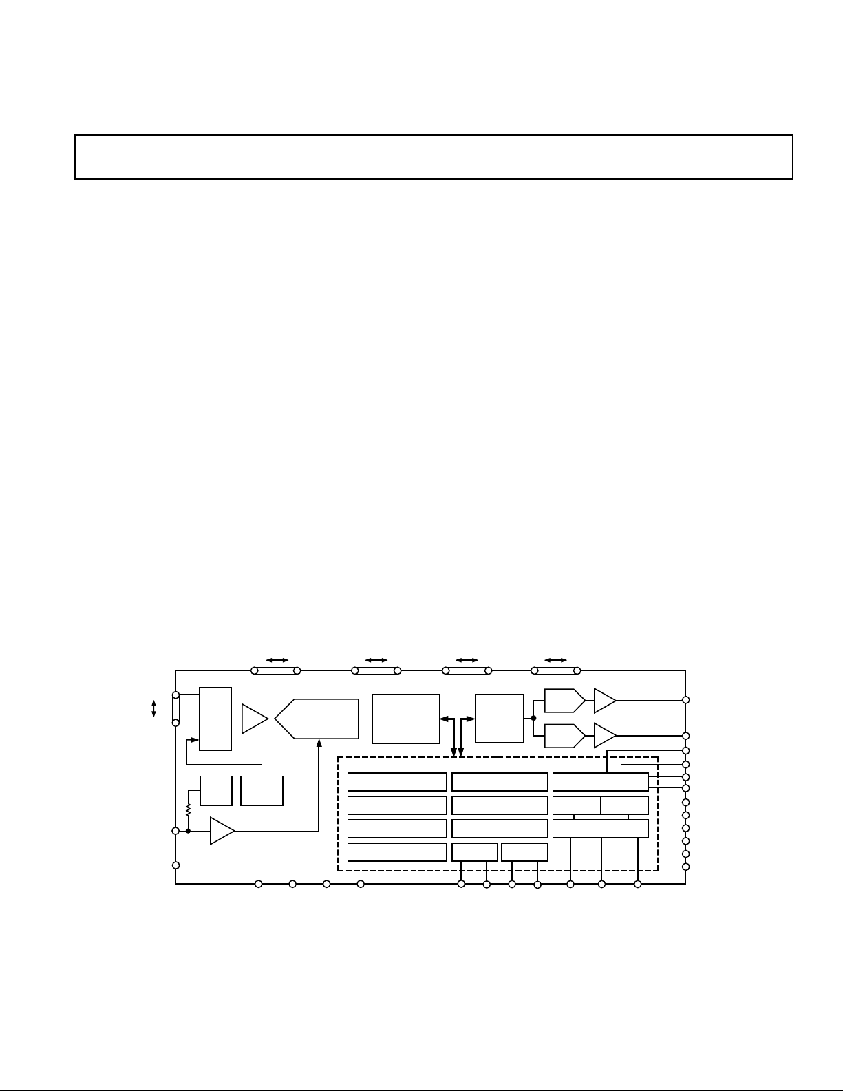
AIN0 (P1.0)
AIN
AIN7 (P1.7)
V
REF
C
REF
MUX
2.5V
REF
BUF
T/H
TEMP
SENSOR
Requirements)
PP
FUNCTIONAL BLOCK DIAGRAM
12-BIT
SUCCESSIVE
APPROXIMATION
ADC
12-Bit ADC with Embedded FLASH MCU
ADuC812
APPLICATIONS
Intelligent Sensors (IEEE 1451.2-Compatible)
Battery Powered Systems (Portable PCs, Instruments,
Monitors)
Transient Capture Systems
DAS and Communications Systems
GENERAL DESCRIPTION
The ADuC812 is a fully integrated 12-bit data acquisition
system incorporating a high performance self-calibrating
multichannel ADC, two 12-bit DACs and programmable 8-bit
(8051-compatible) MCU on a single chip.
The programmable 8051-compatible core is supported by
8K bytes Flash/EE program memory, 640 bytes Flash/EE data
memory and 256 bytes data SRAM on-chip.
Additional MCU support functions include Watchdog Timer,
ADC
CONTROL
AND
CALIBRATION
LOGIC
8051-COMPATIBLE
MICROCONTROLLER
8K BYTES FLASH/EE
PROGRAM MEMORY
640 BYTES FLASH/EE
DATA MEMORY
256 8 USER
RAM
Power Supply Monitor and ADC DMA functions. 32 Programmable I/O lines, I
Serial Port I/O are provided for multiprocessor interfaces and
I/O expansion.
Normal, idle and power-down operating modes for both the
MCU core and analog converters allow for flexible power management schemes suited to low power applications. The part is
specified for 3 V and 5 V operation over the industrial temperature range and is available in a 52-lead, plastic quad flatpack
package.
DAC
CONTROL
MICROCONTROLLER
POWER SUPPLY
MONITOR
WATCHDOG
TIMER
ON-CHIP SERIAL
DOWN LOADER
OSC
2
C-compatible, SPI and Standard UART
P3.0 P3.7P2.0 P2.7P1.0 P1.7P0.0 P0.7
ADuC812
BUF
BUF
3 16-BIT
TIMER/COUNTERS
2-WIRE
MUX
SPI
DAC0
DAC1
T0 (P3.4)
T1 (P3.5)
T2 (P1.0)
T2EX (P1.1)
INT0 (P3.2)
INT1 (P3.3)
ALE
PSEN
EA
RESET
UART
12-BIT
DAC0
12-BIT
DAC1
SERIAL I/O
AGNDAV
DD
I2C is a registered trademark of Philips Corporation.
MicroConverter is a trademark of Analog Devices, Inc.
SPI is a registered trademark of Motorola Inc.
DGNDDV
DD
REV. 0
Information furnished by Analog Devices is believed to be accurate and
reliable. However, no responsibility is assumed by Analog Devices for its
use, nor for any infringements of patents or other rights of third parties
which may result from its use. No license is granted by implication or
otherwise under any patent or patent rights of Analog Devices.
XTAL
1
One Technology Way, P.O. Box 9106, Norwood, MA 02062-9106, U.S.A.
Tel: 781/329-4700 World Wide Web Site: http://www.analog.com
Fax: 781/326-8703 © Analog Devices, Inc., 1999
(P3.0)
2
(P3.1)
SCLOCK
MOSI/
SDATA
MISO
(P3.3)
RxD
TxD
XTAL

1, 2
ADuC812–SPECIFICATIONS
MCLKIN = 16.0 MHz, DAC V
Load to AGND; RL = 10 k, CL = 100 pF. All specifications TA = T
OUT
(AVDD = DVDD = +3.0 V or +5.0 V 10%, V
to T
MIN
ADuC812BS
Parameter VDD = 5 V VDD = 3 V Units Test Conditions/Comments
ADC CHANNEL SPECIFICATIONS
DC ACCURACY
3, 4
Resolution 12 12 Bits
Integral Nonlinearity ± 1/2 ± 1/2 LSB typ f
± 1.5 LSB max f
± 1.5 ±1.5 LSB typ f
Differential Nonlinearity ± 1 ± 1 LSB typ f
CALIBRATED ENDPOINT ERRORS
5, 6
Offset Error ± 5LSB max
± 1 ± 2 LSB typ
Offset Error Match 1 1 LSB typ
Gain Error ± 6LSB max
± 1 ± 2 LSB typ
Gain Error Match 1.5 1.5 LSB typ
USER SYSTEM CALIBRATION
Offset Calibration Range ± 5 ±5 % of V
Gain Calibration Range ± 2.5 ±2.5 % of V
7
typ
REF
typ
REF
DYNAMIC PERFORMANCE f
Signal-to-Noise Ratio (SNR)
8
70 70 dB typ
Total Harmonic Distortion (THD) –78 –78 dB typ
Peak Harmonic or Spurious Noise –78 –78 dB typ
ANALOG INPUT
Input Voltage Ranges 0 to V
REF
0 to V
REF
Volts
Leakage Current ± 10 µA max
± 1+1 µA typ
Input Capacitance 20 20 pF max
TEMPERATURE SENSOR
9
Voltage Output at +25°C 600 600 mV typ Measured On-Chip via a Typical
Voltage TC –3.0 –3.0 mV/°C typ ± 0.5 LSB (610 µV) Accurate ADC
DAC CHANNEL SPECIFICATIONS
DC ACCURACY
10
Resolution 12 12 Bits
Relative Accuracy ± 3 ± 3 LSB typ
Differential Nonlinearity ±0.5 ±1 LSB typ Guaranteed 12-Bit Monotonic
Offset Error ± 50 mV max
± 25 ± 25 mV typ
Full-Scale Error ± 25 mV max
± 10 ± 10 mV typ
Full-Scale Mismatch ± 0.5 ± 0.5 % typ % of Full-Scale on DAC1
ANALOG OUTPUTS
Voltage Range_0 0 to V
Voltage Range_1 0 to V
REF
DD
0 to V
0 to V
REF
DD
V typ
V typ
Resistive Load 10 10 kΩ typ
Capacitive Load 100 100 pF typ
Output Impedance 0.5 0.5 Ω typ
I
SINK
50 50 µA typ
= 2.5 V Internal Reference,
REF
, unless otherwise noted.)
MAX
= 100 kHz
SAMPLE
= 100 kHz
SAMPLE
= 200 kHz
SAMPLE
= 100 kHz. Guaranteed No
SAMPLE
Missing Codes at 5 V
= 10 kHz Sine Wave
IN
f
= 100 kHz
SAMPLE
–2–
REV. 0

ADuC812
ADuC812BS
Parameter VDD = 5 V VDD = 3 V Units Test Conditions/Comments
DAC AC CHARACTERISTICS
Voltage Output Settling Time 15 15 µs typ Full-Scale Settling Time to
Within 1/2 LSB of Final Value
Digital-to-Analog Glitch Energy 10 10 nV sec typ 1 LSB Change at Major Carry
REFERENCE INPUT/OUTPUT
REFIN Input Voltage Range 2.3/V
DD
Input Impedance 150 150 kΩ typ
REF
Output Voltage 2.45/2.55 V min/max
OUT
2.5 2.5 V typ
REF
FLASH/EE MEMORY PERFORMANCE
CHARACTERISTICS
Tempco 40 40 ppm/°C typ
OUT
11, 12
Endurance 10,000 Cycles min
50,000 50,000 Cycles typ
Data Retention 10 Years min
WATCHDOG TIMER
CHARACTERISTICS
Oscillator Frequency 64 64 kHz typ
POWER SUPPLY MONITOR
CHARACTERISTICS
Power Supply Trip Point Accuracy ± 2.5 % of Selected
± 1.0 ±1.0 % of Selected
DIGITAL INPUTS
Input High Voltage (V
Input Low Voltage (V
) 2.4 V min
INH
) 0.8 V max
INL
Input Leakage Current (Port 0, EA) ± 10 µA max V
± 1 ± 1 µA typ VIN = 0 V or V
Logic 1 Input Current
(All Digital Inputs) ± 10 µA max V
± 1 ± 1 µA typ VIN = V
Logic 0 Input Current (Port 1, 2, 3) –80 µA max
–40 –40 µA typ V
Logic 1-0 Transition Current (Port 1, 2, 3) –700 µA max V
–400 –400 µA typ V
Input Capacitance 10 10 pF typ
2.3/V
DD
V min/max
Nominal Trip
Point Voltage
max
Nominal Trip
Point Voltage
typ
= 0 V or V
IN
= V
IN
DD
DD
= 450 mV
IL
= 2 V
IL
= 2 V
IL
DD
DD
REV. 0 –3–

ADuC812–SPECIFICATIONS
1, 2
ADuC812BS
Parameter VDD = 5 V VDD = 3 V Units Test Conditions/Comments
DIGITAL OUTPUTS
Output High Voltage (VOH) 2.4 V min VDD = 4.5 V to 5.5 V
= 80 µA
I
4.0 2.6 V typ V
Output Low Voltage (V
OL
)
ALE, PSEN, Ports 0 and 2 0.4 V max I
0.2 0.2 V typ I
Port 3 0.4 V max I
0.2 0.2 V typ I
Floating State Leakage Current ± 10 µA max
± 5 ± 5 µA typ
Floating State Output Capacitance 10 10 pF typ
POWER REQUIREMENTS
IDD Normal Mode
16
13, 14, 15
42 mA max MCLKIN = 16 MHz
32 16 mA typ MCLKIN = 16 MHz
26 12 mA typ MCLKIN = 12 MHz
8 3 mA typ MCLKIN = 1 MHz
Idle Mode 25 mA max MCLKIN = 16 MHz
I
DD
18 17 mA typ MCLKIN = 16 MHz
15 6 mA typ MCLKIN = 12 MHz
7 2 mA typ MCLKIN = 1 MHz
50 50 µA max
Power-Down Mode
I
DD
17
55 µA typ
NOTES
1
Specifications apply after calibration.
2
Temperature range –40°C to +85°C.
3
Linearity is guaranteed during normal MicroConverter Core operation.
4
Linearity may degrade when programming or erasing the 640 Byte Flash/EE space during ADC conversion times due to on-chip charge pump activity.
5
Measured in production at VDD = 5 V after Software Calibration Routine at +25°C only.
6
User may need to execute Software Calibration Routine to achieve these specifications, which are configuration dependent.
7
The offset and gain calibration spans are defined as the voltage range of user system offset and gain errors that the ADuC812 can compensate.
8
SNR calculation includes distortion and noise components.
9
The temperature sensor will give a measure of the die temperature directly, air temperature can be inferred from this result.
10
DAC linearity is calculated using:
reduced code range of 48 to 4095, 0 to V
reduced code range of 48 to 3995, 0 to VDD range
DAC output load = 10 kΩ and 50 pF.
11
Flash/EE Memory Performance Specifications are qualified as per JEDEC Specification A103 (Data Retention) and JEDEC Draft Specification All7 (Endurance).
12
Endurance Cycling is evaluated under the following conditions:
Mode = Byte Programming, Page Erase Cycling
Cycle Pattern = 00Hex to FFHex
Erase Time = 20 ms
Program Time = 100 µs
13
IDD at other MCLKIN frequencies is typically given by:
Normal Mode (VDD = 5 V): IDD = (1.6 × MCLKIN) + 6
Normal Mode (VDD = 3 V): IDD = (0.8 × MCLKIN) + 3
Idle Mode (VDD = 5 V): IDD = (0.75 × MCLKIN) + 6
Idle Mode (VDD = 3 V): IDD = (0.25 × MCLKIN) + 3
Where MCLKIN is the oscillator frequency in MHz and resultant IDD values are in mA.
14
IDD Currents are expressed as a summation of analog and digital power supply currents during normal MicroConverter operation.
15
IDD is not measured during Flash/EE program or erase cycles; IDD will typically increase by 10 mA during these cycles.
16
Analog IDD = 2 mA (typ) in normal operation (internal V
17
EA = Port0 = DVDD, XTAL1 (Input) tied to DVDD, during this measurement.
Typical specifications are not production tested, but are supported by characterization data at initial product release.
Specifications subject to change without notice.
Please refer to User Guide, Quick Reference Guide, Application Notes and Silicon Errata Sheet at www.analog.com/microconverter for additional information.
REF
range
, ADC and DAC peripherals powered on).
REF
SOURCE
= 2.7 V to 3.3 V
DD
= 20 µA
I
SOURCE
= 1.6 mA
SINK
= 1.6 mA
SINK
= 8 mA
SINK
= 8 mA
SINK
–4–
REV. 0
ADuC812
WARNING!
ESD SENSITIVE DEVICE
ABSOLUTE MAXIMUM RATINGS*
(TA = +25°C unless otherwise noted)
AVDD to DVDD . . . . . . . . . . . . . . . . . . . . . . .–0.3 V to +0.3 V
AGND to DGND . . . . . . . . . . . . . . . . . . . . –0.3 V to +0.3 V
DV
to DGND, AVDD to AGND . . . . . . . . . –0.3 V to +7 V
DD
Digital Input Voltage to DGND . . . . . –0.3 V, DV
Digital Output Voltage to DGND . . . . –0.3 V, DV
V
to AGND . . . . . . . . . . . . . . . . . . . –0.3 V, AVDD + 0.3 V
REF
Analog Inputs to AGND . . . . . . . . . . . . –0.3 V, AV
+ 0.3 V
DD
+ 0.3 V
DD
+ 0.3 V
DD
Operating Temperature Range
Industrial (B Version) . . . . . . . . . . . . . . . . –40°C to +85°C
Storage Temperature Range . . . . . . . . . . . . –65°C to +150°C
Junction Temperature . . . . . . . . . . . . . . . . . . . . . . . . .+150°C
θ
Thermal Impedance . . . . . . . . . . . . . . . . . . . . . . . 90°C/W
JA
Lead Temperature, Soldering
Vapor Phase (60 sec) . . . . . . . . . . . . . . . . . . . . . . . .+215°C
Infrared (15 sec) . . . . . . . . . . . . . . . . . . . . . . . . . . .+220°C
*Stresses above those listed under Absolute Maximum Ratings may cause perma-
nent damage to the device. This is a stress rating only; functional operation of the
device at these or any other conditions above those listed in the operational
sections of this specification is not implied. Exposure to absolute maximum rating
conditions for extended periods may affect device reliability.
ORDERING GUIDE
P1.0/ADC0/T2
P1.1/ADC1/T2EX
P1.2/ADC2
P1.3/ADC3
AV
AGND
C
REF
V
REF
DAC0
DAC1
P1.4/ADC4
P1.5/ADC5/SS
P1.6/ADC6
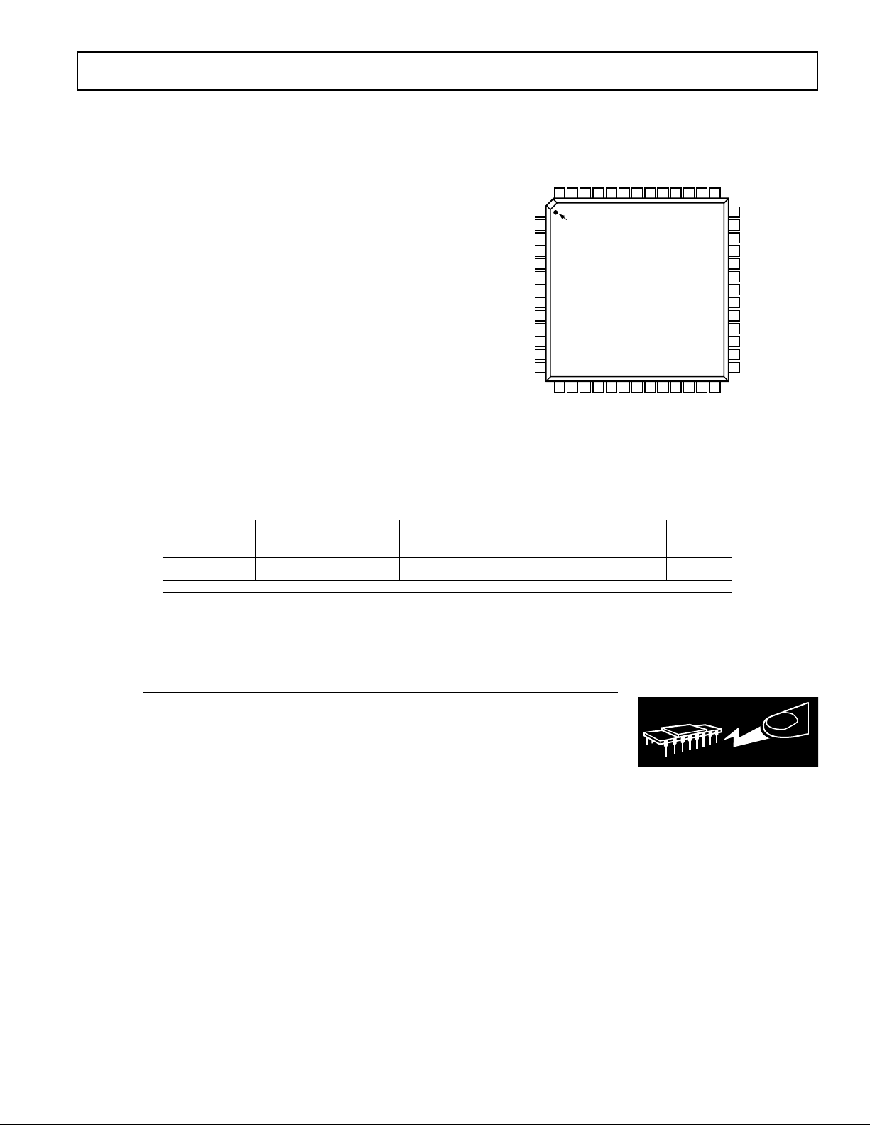
PIN CONFIGURATION
DD
P0.5/AD5
P0.6/AD6
P0.7/AD7
52 51 50 49 48 43 42 41 4047 46 45 44
1
PIN 1
IDENTIFIER
2
3
4
5
DD
6
7
8
9
10
11
12
13
14 15 16 17 18 19 20 21 22 23 24 25 26
RESET
P1.7/ADC7
DV
P0.4/AD4
(Not to Scale)
P3.1/TxD
P3.0/RxD
DGND
ADuC812
TOP VIEW
P3.2/INT0
P3.3/INT1/MISO
P0.2/AD2
P0.3/AD3
DD
DV
DGND
P0.0/AD0
P0.1/AD1
P3.4/T0
P3.5/T1/CONVST
ALE
P3.6/WR
PSEN
P3.7/RD
EA
SCLOCK
39
P2.7/A15/A23
38
P2.6/A14/A22
37
P2.5/A13/A21
36
P2.4/A12/A20
35
DGND
34
DV
DD
33
XTAL2 (OUTPUT)
32
XTAL1 (INPUT)
31
P2.3/A11/A19
30
P2.2/A10/A18
29
P2.1/A9/A17
28
P2.0/A8/A16
27
SDATA/MOSI
Temperature Package Package
Model Range Description Option
ADuC812BS –40°C to +85°C 52-Lead Plastic Quad Flatpack S-52
QuickStart™ Development System
Eval-ADuC812QS
CAUTION
ESD (electrostatic discharge) sensitive device. Electrostatic charges as high as 4000 V readily
accumulate on the human body and test equipment and can discharge without detection.
Although the ADuC812 features proprietary ESD protection circuitry, permanent damage may
occur on devices subjected to high energy electrostatic discharges. Therefore, proper ESD
precautions are recommended to avoid performance degradation or loss of functionality.
REV. 0
–5–

ADuC812
PIN FUNCTION DESCRIPTIONS
Mnemonic Type Function
DV
DD
AV
DD
C
REF
V
REF
AGND G Analog Ground. Ground Reference point for the analog circuitry.
P1.0–P1.7 I Port 1 is an 8-bit Input Port only. Unlike other Ports, Port 1 defaults to Analog Input Mode, to configure
ADC0–ADC7 I Analog Inputs. Eight single-ended analog inputs. Channel selection is via ADCCON2 SFR.
T2 I Timer 2 Digital Input. Input to Timer/Counter 2. When Enabled, Counter 2 is incremented in response to
T2EX I Digital Input. Capture/Reload trigger for Counter 2 and also functions as an Up/Down control input for
SS I Slave Select input for the SPI interface.
SDATA I/O User selectable, I
SCLOCK I/O Serial Clock pin for I
MOSI I/O SPI Master Output/Slave Input Data I/O pin for SPI interface.
MISO I/O Master Input/Slave Output Data I/O pin for SPI Serial Interface.
DAC0 O Voltage Output from DAC0.
DAC1 O Voltage Output from DAC1.
RESET I Digital Input. A high level on this pin for 24 master clock cycles while the oscillator is running resets the
P3.0–P3.7 I/O Port 3 is a bidirectional port with internal pull-up resistors. Port 3 pins that have 1s written to them are
RxD I/O Receiver Data Input (asynchronous) or Data Input/ Output (synchronous) of serial (UART) port.
TxD O Transmitter Data Output (asynchronous) or Clock Output (synchronous) of serial (UART) port.
INT0 I Interrupt 0, programmable edge or level triggered Interrupt input, which can be programmed to one of two
INT1 I Interrupt 1, programmable edge or level triggered Interrupt input, which can be programmed to one of two
T0 I Timer/Counter 0 Input.
T1 I Timer/Counter 1 Input.
CONVST I Active low Convert Start Logic input for the ADC block when the external Convert start function is en-
WR O Write Control Signal, Logic Output. Latches the data byte from Port 0 into the external data memory.
RD O Read Control Signal, Logic Output. Enables the external data memory to Port 0.
XTAL2 O Output of the inverting oscillator amplifier.
XTAL1 I Input to the inverting oscillator amplifier and input to the internal clock generator circuits.
DGND G Digital Ground. Ground reference point for the digital circuitry.
P2.0–P2.7 I/O Port 2 is a bidirectional port with internal pull-up resistors. Port 2 pins that have 1s written to them are
(A8–A15) pulled high by the internal pull-up resistors, and in that state they can be used as inputs. As inputs Port 2
(A16–A23) pins being pulled externally low will source current because of the internal pull-up resistors. Port 2 emits
PSEN O Program Store Enable, Logic Output. This output is a control signal that enables the external program
P Digital Positive Supply Voltage, +3 V or +5 V nominal.
P Analog Positive Supply Voltage, +3 V or +5 V nominal.
I Decoupling pin for on-chip reference. Connect 0.1 µF between this pin and AGND.
I/O Reference Input/Output. This pin is connected to the internal reference through a series resistor and is the
reference source for the analog-to-digital converter. The nominal internal reference voltage is 2.5 V and this
appears at the pin (once the ADC or DAC peripherals are enabled). This pin can be overdriven by an external reference.
any of these Port Pins as a digital input, write a “0” to the port bit. Port 1 pins are multifunction and share
the following functionality.
a 1 to 0 transition of the T2 input.
Counter 2.
2
C-Compatible Input/Output pin or SPI Data Input/Output pin.
2
C-Compatible or SPI serial interface clock.
device.
pulled high by the internal pull-up resistors, and in that state they can be used as inputs. As inputs Port 3
pins being pulled externally low will source current because of the internal pull-up resistors. Port 3 pins also
contain various secondary functions which are described below.
priority levels. This pin can also be used as a gate control input to Timer 0.
priority levels. This pin can also be used as a gate control input to Timer 1.
abled. A low-to-high transition on this input puts the track/hold into its hold mode and starts conversion.
the high order address bytes during fetches from external program memory and middle and high order
address bytes during accesses to the external 24-bit external data memory space.
memory to the bus during external fetch operations. It is active every six oscillator periods except during
external data memory accesses. This pin remains high during internal program execution. PSEN can also be
used to enable serial download mode when pulled low through a resistor on power-up or RESET.
–6–
REV. 0

ADuC812
Mnemonic Type Function
ALE O Address Latch Enable, Logic Output. This output is used to latch the low byte (and middle byte for 24-bit
address space accesses) of the address into external memory during normal operation. It is activated every
six oscillator periods except during an external data memory access.
EA I External Access Enable, Logic Input. When held high, this input enables the device to fetch code from
internal program memory locations 0000H to 1FFFH. When held low this input enables the device to fetch
all instructions from external program memory.
P0.7–P0.0 I/O Port 0 is an 8-bit open drain bidirectional I/O port. Port 0 pins that have 1s written to them float and in that
(A0–A7) state can be used as high impedance inputs. Port 0 is also the multiplexed low order address and data bus
during accesses to external program or data memory. In this application it uses strong internal pull-ups
when emitting 1s.
TERMINOLOGY
ADC SPECIFICATIONS
Integral Nonlinearity
This is the maximum deviation of any code from a straight line
passing through the endpoints of the ADC transfer function.
The endpoints of the transfer function are zero scale, a point
1/2 LSB below the first code transition and full scale, a point
1/2 LSB above the last code transition.
Differential Nonlinearity
This is the difference between the measured and the ideal 1 LSB
change between any two adjacent codes in the ADC.
Offset Error
This is the deviation of the first code transition (0000 . . . 000)
to (0000 . . . 001) from the ideal, i.e., +1/2 LSB.
Full-Scale Error
This is the deviation of the last code transition from the ideal
AIN voltage (Full Scale – 1.5 LSB) after the offset error has
been adjusted out.
Signal to (Noise + Distortion) Ratio
This is the measured ratio of signal to (noise + distortion) at the
output of the A/D converter. The signal is the rms amplitude of
the fundamental. Noise is the rms sum of all nonfundamental
signals up to half the sampling frequency (f
/2), excluding dc.
S
The ratio is dependent upon the number of quantization levels
in the digitization process; the more levels, the smaller the quantization noise. The theoretical signal to (noise +distortion) ratio
for an ideal N-bit converter with a sine wave input is given by:
Signal to (Noise + Distortion) = (6.02N + 1.76) dB
Thus for a 12-bit converter, this is 74 dB.
Total Harmonic Distortion
Total Harmonic Distortion is the ratio of the rms sum of the
harmonics to the fundamental.
DAC SPECIFICATIONS
Relative Accuracy
Relative accuracy or endpoint linearity is a measure of the maximum deviation from a straight line passing through the endpoints of the DAC transfer function. It is measured after
adjusting for zero error and full-scale error.
Voltage Output Settling Time
This is the amount of time it takes for the output to settle to a
specified level for a full-scale input change.
Digital to Analog Glitch Impulse
This is the amount of charge injected into the analog output
when the inputs change state. It is specified as the area of the
glitch in nV sec.
REV. 0
–7–
ADuC812
ADuC812 ARCHITECTURE, MAIN FEATURES
The ADuC812 is a highly integrated high accuracy 12-bit data
acquisition system. At its core, the ADuC812 incorporates a high
performance 8-bit (8051-Compatible) MCU with on-chip reprogrammable nonvolatile Flash/EE program memory controlling a
multichannel (8-input channels), 12-bit ADC.
The chip incorporates all secondary functions to fully support the
programmable data acquisition core. These secondary functions
include User Flash/EE Data Memory, Watchdog Timer (WDT),
Power Supply Monitor (PSM) and various industry-standard
parallel and serial interfaces.
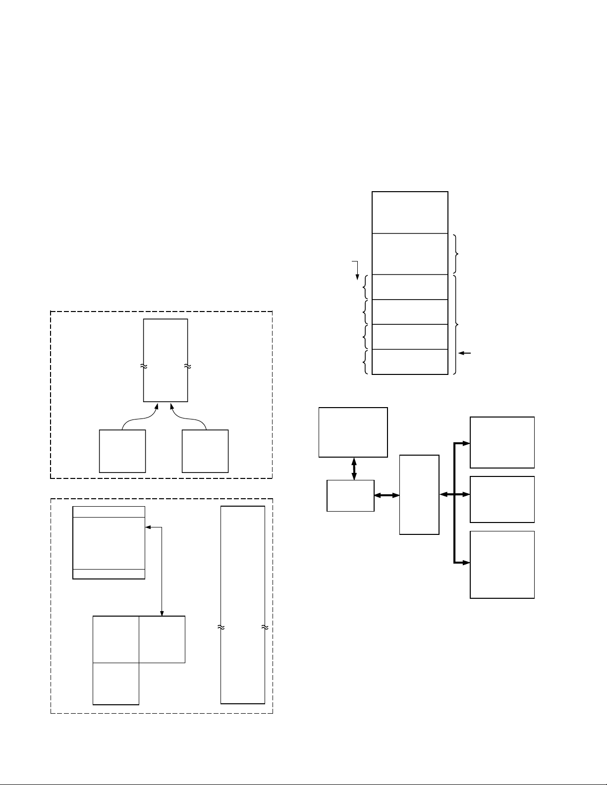
ADuC812 MEMORY ORGANIZATION
As with all 8051-compatible devices, the ADuC812 has separate
address spaces for Program and Data memory as shown in Figure 1. Also as shown in Figure 1, an additional 640 Bytes of
Flash/EE Data Memory are available to the user. The Flash/EE
Data Memory area is accessed indirectly via a group of control
registers mapped in the Special Function Register (SFR) area.
PROGRAM MEMORY SPACE
READ ONLY
FFFFFFH
EXTERNAL
PROGRAM
MEMORY
SPACE
The lower 128 bytes of internal data memory are mapped as
shown in Figure 2. The lowest 32 bytes are grouped into four
banks of eight registers addressed as R0 through R7. The next
16 bytes (128 bits) above the register banks form a block of bit
addressable memory space at bit addresses 00H through 7FH.
The SFR space is mapped in the upper 128 bytes of internal
data memory space. The SFR area is accessed by direct addressing only and provides an interface between the CPU and all onchip peripherals. A block diagram showing the programming
model of the ADuC812 via the SFR area is shown in Figure 3.
7FH
BANKS
SELECTED
VIA
BITS IN PSW
30H
20H
11
18H
10
10H
01
08H
00
00H
2FH
BIT-ADDRESSABLE SPACE
(BIT ADDRESSES 0–7FH)
1FH
17H
4 BANKS OF 8 REGISTERS
0FH
07H
RESET VALUE OF
STACK POINTER
R0–R7
2000H
1FFFH
EXTERNAL
PROGRAM
MEMORY
0000H
DATA MEMORY SPACE
READ/WRITE
SPECIAL
FUNCTION
REGISTERS
ACCESSIBLE
BY DIRECT
ADDRESSING
ONLY
FFH
80H
EA = 0
SPACE
FFFFFFH
000000H
EXTERNAL
DATA
MEMORY
SPACE
(24-BIT
ADDRESS
SPACE)
9FH
00H
UPPER
LOWER
(PAGE 159)
640 BYTES
FLASH/EE DATA
MEMORY
ACCESSED
INDIRECTLY
VIA SFR
CONTROL REGISTERS
(PAGE 0)
DATA MEMORY
FFH
ACCESSIBLE
80H
7FH
00H
ADDRESSING
ADDRESSING
128
128
EA = 1
INTERNAL
8K BYTE
FLASH/EE
PROGRAM
MEMORY
INTERNAL
SPACE
BY
INDIRECT
ONLY
ACCESSIBLE
BY
DIRECT
AND
INDIRECT
Figure 1. ADuC812 Program and Data Memory Maps
Figure 2. Lower 128 Bytes of Internal RAM
8K BYTE
ELECTRICALLY
REPROGRAMMABLE
NONVOLATILE
FLASH/EE PROGRAM
MEMORY
8051-
COMPATIBLE
CORE
128-BYTE
SPECIAL
FUNCTION
REGISTER
AREA
640-BYTE
ELECTRICALLY
REPROGRAMMABLE
NONVOLATILE
FLASH/EE DATA
MEMORY
SELF-CALIBRATING
8-CHANNEL
HIGH SPEED
12-BIT ADC
OTHER ON-CHIP
PERIPHERALS
TEMPERATURE
SENSOR
2 12-BIT DACs
SERIAL I/O
PARALLEL I/O
WDT
PSM
Figure 3. ADuC812 Programming Model
ADC CIRCUIT INFORMATION
General Overview
The ADC conversion block incorporates a 5 µs, 8-channel,
12-bit, single supply A/D converter. This block provides the
user with multichannel mux, track/hold, on-chip reference,
calibration features and A/D converter. All components in this
block are easily configured via a 3-register SFR interface.
The A/D converter consists of a conventional successiveapproximation converter based around a capacitor DAC. The
converter accepts an analog input range of 0 to +V
. A high
REF
precision, low drift and factory calibrated 2.5 V reference is
–8–
REV. 0
ADuC812
provided on-chip. The internal reference may be overdriven via
the external V
range 2.3 V to AV
pin. This external reference can be in the
REF
.
DD
Single step or continuous conversion modes can be initiated in
software or, alternatively, by applying a convert signal to an
external Pin 25 (CONVST). Timer 2 can also be configured
to generate a repetitive trigger for ADC conversions. The ADC
may be configured to operate in a DMA Mode whereby the
ADC block continuously converts and captures samples to an
external RAM space without any interaction from the MCU
core. This automatic capture facility can extend through a
16 MByte external Data Memory space.
The ADuC812 is shipped with factory programmed calibration
coefficients that are automatically downloaded to the ADC on
power-up, ensuring optimum ADC performance. The ADC
core contains internal Offset and Gain calibration registers, a
software calibration routine is provided to allow the user to
overwrite the factory programmed calibration coefficients if
required, thus minimizing the impact of endpoint errors in the
users target system.
A voltage output from an on-chip temperature sensor proportional to absolute temperature can also be routed through the
front-end ADC multiplexor (effectively a 9th ADC channel
input) facilitating a temperature sensor implementation.
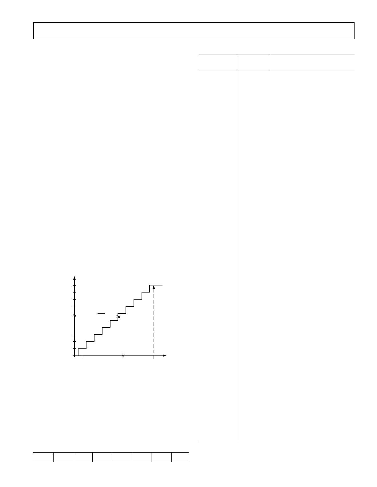
ADC Transfer Function
The analog input range for the ADC is 0 V to V
. For this
REF
range, the designed code transitions occur midway between
successive integer LSB values (i.e., 1/2 LSB, 3/2 LSBs,
5/2 LSBs . . . FS –3/2 LSBs). The output coding is straight
binary with 1 LSB = FS/4096 or 2.5 V/4096 = 0.61 mV when
= 2.5 V. The ideal input/output transfer characteristic for
V
REF
the 0 to V
range is shown in Figure 4.
REF
OUTPUT
CODE
111...111
111...110
111...101
111...100
000...011
000...010
000...001
000...000
1LSB
0V
1LSB =
FS
4096
VOLTAGE INPUT
+FS
–1LSB
Figure 4. ADuC812 ADC Transfer Function
SFR Interface to ADC Block
The ADC operation is fully controlled via three SFRs, namely:
ADCCON1 – (ADC Control SFR #1)
The ADCCON1 register controls conversion and acquisition
times, hardware conversion modes and power-down modes as
detailed below.
SFR Address: EFH
SFR Power-On Default Value: 20H
Bit Addressable: NO
MD1 MD0 CK1 CK0 AQ1 AQ0 T2C EXC
Table I. ADCCON1 SFR Bit Designations
Bit Bit
Location Mnemonic Description
ADCCON1.7 MD1 The mode bits (MD1, MD0)
ADCCON1.6 MD0 select the active operating mode
of the ADC as follows:
MD1 MD0 Active Mode
0 0 ADC powered down.
0 1 ADC normal mode
1 0 ADC powered down
if not executing a
conversion cycle.
1 1 ADC standby if not
executing a conversion cycle.
ADCCON1.5 CK1 The ADC clock divide bits (CK1,
ADCCON1.4 CK0 CK0) select the divide ratio for
the master clock used to generate
the ADC clock. An ADC conversion will require 16 ADC
clocks in addition to the selected
number of acquisition clocks (see
AQ0/AQ1 below). The divider
ratio is selected as follows:
CK1 CK0 MCLK Divider
001
012
104
118
ADCCON1.3 AQ1 The ADC acquisition select bits
ADCCON1.2 AQ0 (AQ1, AQ0) select the time avail-
able for the input track/hold
amplifier to acquire the input
signal and is selected as follows:
AQ1 AQ0 #ADC Clks
001
012
103
114
Note: for analog input source
impedances of <8 kΩ, the default
AQ0/AQ1 selection of 00, i.e., 1
Acquisition Clock will suffice. For
source impedances greater than
this, it is recommended that you
increase the acquisition clock
selection to 2, 3 or 4 clocks.
ADCCON1.1 T2C The Timer 2 conversion bit (T2C)
is set to enable the Timer 2 overflow bit to be used as the ADC
convert start trigger input.
ADCCON1.0 EXC The external trigger enable bit
(EXC) is set to allow the external
Pin 23 (CONVST) to be used as
the active low convert start input.
This input should be an active low
pulse (100 ns minimum pulsewidth)
at the required sample rate.
Note: In standby mode the ADC V
powered down mode all ADC peripherals are powered down thus minimizing
current consumption. Typical ADC current consumption is 1.6 mA at VDD = 5 V.
circuits are maintained on, while in
REF
REV. 0
–9–

ADuC812
ADCCON2 – (ADC Control SFR #2)
The ADCCON2 register controls ADC channel selection and
conversion modes as detailed below.
SFR Address: D8H
SFR Power On Default Value: 00H
Bit Addressable: YES
ADCI DMA CCONV SCONV CS3 CS2 CS1 CS0
Table II. ADCCON2 SFR Bit Designations
Bit Bit
Location Mnemonic Description
ADCCON2.7 ADCI The ADC interrupt bit (ADCI) is
set by hardware at the end of a
single ADC conversion cycle or at
the end of a DMA block conversion. ADCI is cleared by hardware
when the PC vectors to the ADC
Interrupt Service Routine.
ADCCON2.6 DMA The DMA mode enable bit (DMA)
is set by the user to initiate a preconfigured ADC DMA mode operation. A more detailed description of
this mode is given below.
ADCCON2.5 CCONV The continuous conversion bit
(CCONV) is set by the user to
initiate the ADC into a continuous
mode of conversion. In this mode
the ADC starts converting based on
the timing and channel configuration already set up in the ADCCON
SFRs, the ADC automatically starts
an other conversion once a previous
conversion cycle has completed.
ADCCON2.4 SCONV The single conversion bit
(SCONV) is set by the user to
initiate a single conversion cycle.
The SCONV bit is automatically
reset to “0” on completion of the
single conversion cycle.
ADCCON2.3 CS3 The channel selection bits (CS3-0)
ADCCON2.2 CS2 allow the user to program the
ADCCON2.1 CS1 ADC channel selection under
ADCCON2.0 CS0 software control. Once a conver-
sion is initiated the channel
converted will be that pointed to
by these channel selection bits. In
DMA mode the channel selection
is derived from the channel ID
written to the external memory.
CS3 CS2 CS1 CS0 CH#
00000
00011
00102
00113
01004
01015
01106
01117
1000Temp Sensor
1 X X X Other
Combinations
1111DMA STOP
ADCCON3 – (ADC Control SFR #3)
The ADCCON3 register gives user software an indication of
ADC busy status.
SFR Address: F5H
SFR Power On Default Value: 00H
Bit Addressable: NO
BUSY RSVD RSVD RSVD CTYP CAL1 CAL0 CALST
Table III. ADCCON3 SFR Bit Designations
Bit Bit
Location Mnemonic Description
ADCCON3.7 BUSY The ADC busy status bit (BUSY)
is a read-only status bit that is set
during a valid ADC conversion or
calibration cycle. Busy is automatically cleared by the core at the
end of conversion or calibration.
ADCCON3.6 RSVD ADCCON3.0–3.6 are reserved
ADCCON3.5 RSVD (RSVD) for internal use. These
ADCCON3.4 RSVD bits will read as zero and should
ADCCON3.3 RSVD only be written as zero by user
ADCCON3.2 RSVD software.
ADCCON3.1 RSVD
ADCCON3.0 RSVD
ADC Internal Reference
If the internal reference is being used, both the V
REF
and C
REF
pins should be decoupled with 100 nF capacitors to AGND.
These decoupling capacitors should be placed very close to the
V
REF
and C
pins. For specified performance, it is recom-
REF
mended that when using an external reference, this reference
should be between 2.3 V and the analog supply AV
DD
.
If the internal reference is required for use external to the
MicroConverter, it should be buffered at the V
pin and a
REF
100 nF capacitor should be connected from this pin to AGND.
The internal 2.5 V is factory calibrated to an absolute accuracy
of 2.5 V ±50 mV. It should also be noted that the internal V
REF
will remain powered down until either of the DACs or the ADC
peripheral blocks are powered on by their respective enable bits.
Calibration
The ADC block also has four associated calibration SFRs.
These SFR’s drive calibration logic ensuring optimum performance from the 12-bit ADC at all times. As part of the poweron reset configuration, these SFRs are configured automatically
and transparently from factory programmed calibration constants. In many applications use of factory programmed calibration constants will suffice; however, these calibration SFRs may
be overwritten by user code to further compensate for systemdependent offset and gain errors.
Calibration Overview
The ADC block incorporates calibration hardware that ensures
optimum performance from the ADC at all times. The calibration modes are exercised as part of the ADuC812 internal factory
final test routines. The factory calibration results are stored in
Flash memory and are automatically downloaded on any poweron-reset event to initialize the ADC calibration registers. In
–10–
REV. 0

many applications this autocalibration download function suffices. Alternatively, a device calibration can be easily initiated by
user software to compensate for significant changes in operating
conditions (CLK frequency, analog input range, reference voltage and supply voltages).
This in-circuit software calibration feature allows the user to
remove various system and reference related errors (whether it
be internal or external reference) and to make use of the full
dynamic range of the ADC by adjusting the analog input range
of the part for a specific system. Contact Analog Devices, Inc.
for further details on the implementation of the software calibration routine in your applications.
ADC MODES OF OPERATION
Typical Operation
Once configured via the ADCCON 1-3 SFRs (shown previously) the ADC will convert the analog input and provide an
ADC 12-bit result word in the ADCDATAH/L SFRs. The top
four bits of the ADCDATAH SFR will be written with the
channel selection bits to identify the channel result. The format
of the ADC 12-bit result word is shown in Figure 5.
ADCDATAH SFR
CH–ID
TOP 4 BITS
HIGH 4 BITS OF
ADC RESULT WORD
LOW 8 BITS OF THE
ADC RESULT WORD
ADCDATAL SFR
Figure 5. ADC Result Format
ADC DMA Mode
The on-chip ADC has been designed to run at a maximum speed
of one sample every 5 µs (i.e., 200 kHz sampling rate). Therefore,
in an interrupt driven routine the user software is required to service the interrupt, read the ADC result and store the result for
further post processing, all within 5 µs otherwise the next ADC
sample could be lost. In applications where the ADuC812 cannot sustain the interrupt rate, an ADC DMA Mode is provided.
The ADC DMA Mode is enabled via the DMA enable bit
(ADCCON2.6), which allows the ADC to sample continuously
as per configuration in ADCCON SFRs. Each sample result is
written into an external Static RAM (mapped in the data memory
space) without any interaction from the ADuC812 core. This
mode ensures the ADuC812 can capture a contiguous sample
stream even at full speed ADC update rates.
Before enabling ADC DMA mode the user must first configure
the external SRAM to which the ADC samples will be written.
This consists of writing the required ADC DMA channels into
the channel ID bits (the top four bits) in the external SRAM. A
typical pre
configuration of external memory is sho
wn in Figure 6.
Once the external data memory has been preconfigured, the
DMA address pointer (DMAP, DMAH and DMAL) SFRs are
written. These SFRs should be written with the DMA start
address in external memory. In Figure 6, for example, the DMA
start address is 000000H. The 3-byte start address should be
written in the following order: DMAL, DMAH and DMAP.
The end of a DMA table is signified by writing “1111” into the
channel selection bits field.
ADuC812
00000AH
000000H
1111
0011
0011
1000
0101
0010
Figure 6. Typical DMA External Memory Preconfiguration
The DMA Enable bit (ADCCON2.6, DMA) can now be set to
initiate the DMA conversion and transfer of the results sequentially into external memory. Remember that the DMA mode
will only progress if the user has preconfigured the ADC
conversion time and trigger modes via the ADCCON1 and 2
SFRs. The end of DMA conversion is signified by the ADC
interrupt bit ADCCON2.7.
At the end of ADC DMA Mode, the external data memory
contains the new ADC conversion results as shown in Figure 7.
It should be noted that the channel selection bits are still present
in the result words to identify the individual conversion results.
00000AH
000000H
1111
0011
0011
1000
0101
0010
Figure 7. Typical External Memory Configuration Post
ADC DMA Operation
Micro Operation during ADC DMA Mode
During ADC DMA mode the MicroConverter core is free to
continue code execution, including general housekeeping and
communication tasks. However, it should be noted that MCU
core accesses to Ports 0 and 2 (which, of course, are being used
by the DMA controller) are gated “OFF” during ADC DMA
mode of operation. This means that even though the instruction
that accesses the external Ports 0 or 2 will appear to execute, no
data will be seen at these external port pins as a result.
The MicroConverter core is interrupted once the requested
block of DMA data has been captured and written to external
memory allowing the service routine for this interrupt to postprocess the data without any real time, timing constraints.
SFR Interface to the DAC Block
The ADuC812 incorporates two 12-bit DACs on-chip. DAC
operation is controlled via a single control special function
register and four data special function registers, namely:
DAC0L/DAC1L – Contains the lower 8-bit DAC byte.
DAC0H/DAC1H – Contains the high 4-bit DAC byte.
DACCON – Contains general purpose control bits
required for DAC0 and DAC1 operation.
STOP COMMAND
REPEAT LAST CHANNEL
FOR A VALID STOP
CONDITION
CONVERT ADC CH#3
CONVERT TEMP SENSOR
CONVERT ADC CH#5
CONVERT ADC CH#2
STOP COMMAND
NO CONVERSION
RESULT WRITTEN HERE
CONVERSION RESULT
FOR ADC CH#3
CONVERSION RESULT
FOR TEMP SENSOR
CONVERSION RESULT
FOR ADC CH#5
CONVERSION RESULT
FOR ADC CH#2
REV. 0
–11–

ADuC812
In normal mode of operation each DAC is updated when the
low DAC nibble (DACxL) SFR is written. Both DACs can be
updated simultaneously using the SYNC bit in the DACCON
SFR.
In 8-bit mode of operation, the 8-bit byte written to the DACxL
registers is automatically routed to the top 8 bits of each 12-bit
DAC. The bit designations of the DACCON SFR are shown
below in Table IV.
SFR Address: FDH
SFR Power On Default Value: 04H
Bit Addressable: NO
MODE RNG1 RNG0 CLR1 CLR0 SYNC PD1 PD0
Table IV. DACCON SFR Bit Designations
Bit Bit
Location Mnemonic Description
DACCON.7 MODE The DAC MODE bit sets the
overriding operating mode for
both DACs.
Set to “1” = 8-bit mode (Write 8
bits to DACxL SFR.
Set to “0” = 12-bit mode.
DACCON.6 RNG1 DAC1 range select bit.
Set to “1” = DAC1 range 0–V
Set to “0” = DAC1 range 0–V
DD
REF
.
.
DACCON.5 RNG0 DAC0 range select bit.
Set to “1” = DAC0 range 0–V
Set to “0” = DAC0 range 0–V
DD
REF
.
.
DACCON.4 CLR1 DAC1 clear bit.
Set to “0” = DAC1 output forced
to 0 V.
Set to “1” = DAC1 output
normal.
DACCON.3 CLR0 DAC0 clear bit.
Set to “0” = DAC0 output forced
to 0 V.
Set to “1” = DAC0 output normal.
DACCON.2 SYNC DAC0/1 update synchronization
bit.
When set to “1” the DAC outputs
update as soon as the DACxL
SFRs are written.
The user can simultaneously update both DACs by first updating
the DACxL/H SFRs while SYNC
is “0.”
Both DACs will then update
simultaneously when the SYNC
bit is set to “1.”
DACCON.1 PD1 DAC1 Power-Down Bit.
Set to “1” = Power-On DAC1.
Set to “0” = Power-Off DAC1.
DACCON.0 PD0 DAC0 Power-Down Bit.
Set to “1” = Power-On DAC0.
Set to “0” = Power-Off DAC0.
NONVOLATILE FLASH MEMORY
Flash Memory Overview
The ADuC812 incorporates Flash memory technology on-chip
to provide the user with a nonvolatile, in-circuit reprogrammable, code and data memory space.
Flash memory is the newest type of nonvolatile memory
technology and is based on a single transistor cell architecture.
This technology is basically an outgrowth of EPROM
technology and was developed through the late 1980s.
Flash memory takes the flexible in-circuit reprogrammable
features of EEPROM and combines them with the space
efficient/density features of EPROM (see Figure 8).
Because Flash technology is based on a single transistor cell
architecture, a Flash memory array, like EPROM can be
implemented to achieve the space efficiencies or memory
densities required by a given design.
Like EEPROM, Flash memory can be programmed in-system at
a byte level, although it must be erased first; the erase being
performed in sector blocks. Thus, Flash memory is often and
more correctly referred to as Flash/EE memory.
EPROM
TECHNOLOGY
SPACE EFFICIENT/
DENSITY
FLASH/EE MEMORY
TECHNOLOGY
EEPROM
TECHNOLOGY
IN-CIRCUIT
REPROGRAMMABLE
Figure 8. Flash Memory Development
Overall, Flash/EE memory represents a step closer towards
the ideal memory device that includes nonvolatility, in-circuit
programmability, high density and low cost. Incorporated in
the ADuC812, Flash/EE memory technology allows the user to
update program code space in-circuit without the need to
replace one-time programmable (OTP) devices at remote
operating nodes.
Flash/EE Memory and the ADuC812
The ADuC812 provides two arrays of Flash/EE memory for
user applications.
8K bytes of Flash/EE Program space are provided on-chip to
facilitate code execution without any external discrete ROM
device requirements. The program memory can be programmed
using conventional third party memory programmers. This array
can also be programmed in-circuit, using the serial download
mode provided.
A 640-Byte Flash/EE Data Memory space is also provided onchip. This may be used by the user as a general purpose nonvolatile scratchpad area. User access to this area is via a group of
six SFRs. This space can be programmed at a byte level, although it must first be erased in 4-byte sectors.
Using the Flash/EE Program Memory
This 8K Byte Flash/EE Program Memory array is mapped
into the lower 8K bytes of the 64K bytes program space addressable by the ADuC812 and will be used to hold user code
in typical applications.
–12–
REV. 0

V
DD
GND
P3
PSEN
RST
XTAL1
XTAL2
P0
P1
P2
ALE
ADuC812
+5V
PROGRAM MODE
(SEE TABLE V)
GND
V
DD
PROGRAM
DATA
(D0–D7)
PROGRAM
ADDRESS
(A0–A13)
(P2.0 = A0)
(P1.7 = A13)
WRITE ENABLE
STROBE
The program memory array can be programmed in one of two
modes, namely:
Serial Downloading (In-Circuit Programming)
As part of its factory boot code, the ADuC812 facilitates serial
code download via the standard UART serial port. Serial download mode is automatically entered on power-up if the external
pin, PSEN, is pulled low through an external resistor as shown
in Figure 9. Once in this mode, the user can download code to
the program memory array while the device is sited in its target
application hardware. A PC serial download executable is provided as part of the ADuC812 QuickStart development system.
The Serial Download protocol is detailed in a MicroConverter
Applications Note available from ADI.
PULL PSEN LOW DURING RESET TO
CONFIGURE THE ADuC812
ADuC812
PSEN
1k
FOR SERIAL DOWNLOAD MODE
ADuC812
Figure 10. Flash/EE Memory Parallel Programming
Table V shows the normal parallel programming modes that can
be configured using Port 3 bits.
Table V. Flash Memory Parallel Programing Modes
Port Pins (P3.0–P3.7)
.7 .6 .5 .4 .3 .2 .1 .0 Programming Mode
1 X X X 0 0 0 1 Erase Flash Program
Erase Flash User
1 X X X 0 0 1 1 Read Manufacture and
Chip ID
1 X X X 0 1 0 1 Program Byte
1 X X X 0 1 1 1 Read Byte
1 X X X 1 0 0 1 Reserved
1 X X X 1 0 1 1 Reserved
Any Other Code Redundant
U
sing the Flash/EE Data Memory
The user Flash/EE data memory array consists of 640 bytes that
are configured into 160 (00H to 9FH), 4-byte pages as shown in
Figure 11.
Figure 9. Flash/EE Memory Serial Download Mode
Programming
Parallel Programming
The parallel programming mode is fully compatible with conventional third party Flash or EEPROM device programmers. A
block diagram of the external pin configuration required to
support parallel programming is shown in Figure 10. In this
mode Ports P0, P1 and P2 operate as the external data and
address bus interface, ALE operates as the Write Enable strobe
and Port P3 is used as a general configuration port that configures the device for various program and erase operations during
parallel programming. The high voltage (12 V) supply required
for Flash programming is generated using on-chip charge pumps
to supply the high voltage program lines.
–13–
REV. 0
BYTE 1 BYTE 2 BYTE 3 BYTE 4
9FH
BYTE 1 BYTE 2 BYTE 3 BYTE 4
00H
Figure 11. User Flash/EE Memory Configuration
As with other user peripherals the interface to this memory
space is via a group of registers mapped in the SFR space. A
group of four data registers (EDATA1-4) are used to hold the
4-byte page data just accessed. EADRL is used to hold the 8-bit
address of the page to be accessed. Finally, ECON is an 8-bit
control register that may be written with one of five Flash/EE
memory access commands to enable various read, write, erase
and verify modes.

ADuC812
A block diagram of the SFR registered interface to the User
Flash/EE Memory array is shown in Figure 12.
FUNCTION:
HOLDS THE 8-BIT PAGE
ADDRESS POINTER
9FH
EADRL
00H
FUNCTION:
HOLDS COMMAND WORD
BYTE 1 BYTE 2 BYTE 3 BYTE 4
BYTE 1 BYTE 2 BYTE 3 BYTE 4
ECON COMMAND
INTERPRETER LOGIC
ECON
FUNCTION:
HOLDS THE 4-BYTE
PAGE WORD
EDATA1 (BYTE 1)
EDATA2 (BYTE 2)
EDATA3 (BYTE 3)
EDATA4 (BYTE 4)
FUNCTION:
INTERPRETS THE FLASH
COMMAND WORD
Figure 12. User Flash/EE Memory Control and
Configuration
ECON—Flash/EE Memory Control SFR
This SFR acts as a command interpreter and may be written
with one of five command modes to enable various read, program and erase cycles as detailed in Table VI:
Table VI. ECON–Flash/EE Memory Control Register
Command Modes
Command Byte Command Mode
01H READ COMMAND
Results in four bytes being read into
EDATA 1–4 from memory page location
contained in EADRL .
02H WRITE COMMAND
Results in four bytes (EDATA 1–4) being
written to memory page location in EADRL.
This write command assumes the designated “write” page has been pre-erased.
03H RESERVED COMMAND
“DO NOT USE”
04H VERIFY COMMAND
Allows the user to verify if data in EDATA
1–4 is contained in page location designated
by EADRL. A subsequent read of the
ECON SFR will result in a “zero” being
read if the verification is valid, a nonzero
value will be read to indicate an invalid
verification.
05H ERASE COMMAND
Results in an erase of the 4-byte page
designated in EADRL.
06H ERASE-ALL COMMAND
Results in erase of the full user memory
160-page (640 bytes) array.
07H to FFH RESERVED COMMANDS
Commands reserved for future use.
–14–
Flash/EE Memory Write and Erase Times
The typical program/erase times for the User Flash/EE Memory
are:
Erase Full Array (640 Bytes) – 20 ms
Erase Single Page (4 Bytes) – 20 ms
Program Page (4 Bytes) – 250 µs
Read Page (4 Bytes) – Within Single Instruction Cycle
Using the Flash/EE Memory Interface
As with all Flash/EE memory architectures, the array can be programmed in system at a byte level, although it must be erased
first; the erasure being performed in page blocks (4-byte pages
in this case).
A typical access to the Flash/EE array will involve setting up the
page address to be accessed in the EADRL SFR, configuring the
EDATA1-4 with data to be programmed to the array (the
EDATA SFRs will not be written for read accesses) and finally
writing the ECON command word which initiates one of the
five modes shown in Table VI.
It should be noted that a given mode of operation is initiated as
soon as the command word is written to the ECON SFR. At
this time the core microcontroller operation on the ADuC812
is idled until the requested Program/Read or Erase mode is
completed.
In practice, this means that even though the Flash/EE memory
mode of operation is typically initiated with a 2 machine cycle
MOV instruction (to write to the ECON SFR), the next
instruction will not be executed until the Flash/EE operation
is complete (250 µs or 20 ms later). This means that the core
will not respond to Interrupt requests until the Flash/EE
operation is complete, although the core peripheral functions
like Counter/Timers will continue to count and time as configured
throughout this pseudo-idle period.
ERASE-ALL
Although the 640-byte User Flash/EE array is shipped from the
factory pre-erased, i.e., Byte locations set to FFH, it is nonetheless good programming practice to include an erase-all routine
as part of any configuration/setup code running on the ADuC812.
An “ERASE-ALL” command consists of writing “06H” to the
ECON SFR, which initiates an erase of all 640 byte locations in
the Flash/EE array. This command coded in 8051 assembly
would appear as:
MOV ECON, #06H ; Erase all Command
; 20 ms Duration
PROGRAM A BYTE
In general terms, a byte in the Flash/EE array can only be
programmed if it has previously been erased. To be more specific, a byte can only be programmed if it already holds the value
FFH. Because of the Flash/EE architecture this erasure must
happen at a page level, therefore a minimum of four bytes (1 page)
will be erased when an erase command is initiated.
A more specific example of the Program-Byte process is shown
graphically in Figure 13. In this example the user will write F3H
into the second byte on Page 03H of the User Flash/EE Memory
space.
However, Page 03H already contains four bytes of valid data,
and as the user is only required to modify one of these bytes, the
full page must be first read so that this page can then be erased
without the existing data being lost.
REV. 0

ADuC812
06H A5H 32H 05H 0DH
05H A5H 32H 05H 0DH
04H A5H 32H 05H 0DH
03H A5H 32H 05H 0DH
02H A5H 32H 05H 0DH
01H A5H 32H 05H 0DH
00H A5H 32H 05H 0DH
06H A5H 32H 05H 0DH
05H A5H 32H 05H 0DH
04H A5H 32H 05H 0DH
03H FFH FFH FFH FFH
02H A5H 32H 05H 0DH
01H A5H 32H 05H 0DH
00H A5H 32H 05H 0DH
06H A5H 32H 05H 0DH
05H A5H 32H 05H 0DH
04H A5H 32H 05H 0DH
03H A5H 32H 05H 0DH
02H A5H F3H 05H 0DH
01H A5H 32H 05H 0DH
00H A5H 32H 05H 0DH
0DH
05H
32H
A5H
0DH
05H
F3H
A5H
0DH
05H
F3H
A5H
EDATA4
EDATA3
EDATA2
EDATA1
EDATA4
EDATA3
EDATA2
EDATA1
ERASE
EDATA4
EDATA3
EDATA2
EDATA1
WRITE
READ PAGE 03H
MOV EADRL, #03H ;SET P PAGE
MOV ECON, #01H ;INITIATE READ
WRITE NEW BYTE
TO EDATA2
MOV EDATA2, #0F3H ;WRITE NEW
ERASE PAGE 03H
AND WRITE NEW DATA
TO PAGE 03H
MOV ECON, #05 ;ERASE PAGE
MOV ECON, #02H ;PROGRAM
POINTER
MODE
BYTE
PAGE
Figure 13. User Flash/EE Memory Program Byte Example
The new byte is then written to the EDATA2 SFR, followed by
an ERASE cycle that will ensure this page is erased before the
new page data EDATA1-4 is written back into memory.
If the user attempts to initiate a PROGRAM cycle (ECON
set to 02H) without an ERASE cycle (ECON set to 05H),
then only bit locations set to a “1” would be modified, i.e., the
Flash/EE memory byte location must be pre-erased to allow a
valid write access to the array. It should also be noted that the
time durations for an ERASE-ALL command (640 bytes) and
that for an ERASE page command (four bytes) are identical,
i.e., 20 ms.
This example coded in 8051 assembly would appear as :
MOV EADRL, #03H ; Set Page Pointer
MOV ECON, #01H ; Read Page Command
MOV EDATA2, #0F3H ; Write New Byte
MOV ECON, #02H ; Erase Page Command
MOV ECON, #05H ; Program Page Command
INTERRUPT SYSTEM
The ADuC812 provides nine interrupt sources with two priority
levels. Interrupt priority within a given level is shown in descending order of priority in Figure 14, which gives a general
overview of the interrupt sources and illustrates the request and
control flags. The interrupt vector addresses for corresponding
interrupts are also included in Table VII.
POWER SUPPLY
MONITOR
EXTERNAL INT0
MODE CONVERSION
EXTERNAL INT1
P3.2
END OF ADC
OR ADC DMA
TIMER 0
OVERFLOW
P3.3
TIMER 1
OVERFLOW
SPI/I2C
PORT
UART
TIMER 2
OVERFLOW
P1.1/T2EX
ITO
TCON.0
IT1
TCON.2
I2CCON.0
SPICON.7
SCON.0
SCON.1
T2CON.7
PSMI
I2CI
ISPI
RI
TI
EXEN.2
T2CON.3
PSCON.5
IE0
TCON.1
ADCI
AC2.7
TF0
TCON.5
IE1
TCON.3
TF1
TCON.7
=1
=1
TF2
EXF2
T2CON.6
EPSM
IE2.1
EX0
IE1.0
EADC
IE1.6
ET0
IE1.1
EX1
IE1.2
ET1
IE1.3
ESI
IE2.0
ES
IE1.4
=1
ET2
IE1.5
Figure 14. Interrupt Request Sources
HIGH PRIORITY
LOW PRIORITY
PX0
IP.0
PADC
IP.6
PT0
IP.1
PX1
IP.2
PT1
IP.3
PSI
IP.7
PS
IP.4
PT2
IP.5
REV. 0
–15–

ADuC812
Table VII. Interrupt Vector Addresses
Interrupt Priority
Vector Within
Interrupt Interrupt Name Address Level
PSMI Power Supply Monitor 43H 1
IE0 External INT0 03H 2
ADCI End of ADC Conversion 33H 3
TF0 Timer 0 Overflow 0BH 4
IE1 External INT1 13H 5
TF1 Timer 1 Overflow 1BH 6
I2CI/ISPI Serial Interrupt 3BH 7
RI/TI UART Interrupt 23H 8
TF2/EXF2 Timer 2 Interrupt 2BH 9
Use of Interrupts
To use any of the interrupts on the ADuC812, the following
three steps must be taken.
1. Locate the interrupt service routine at the corresponding
Vector Address of that interrupt. See Table VII above.
2. Set the EA (enable all) bit in the IE SFR to “1.”
3. Set the corresponding individual interrupt bit in the IE
or IE2 SFR to “1.”
Three SFRs are used to enable and set priority for the various
interrupts. The bit designations of these SFRs are shown in
Tables VIII, IX and X. It should be noted that while IE and IP
SFRs are bit addressable, IE2 is byte addressable only.
IE – (Interrupt Enable SFR)
The IE register enables the interrupt system and seven interrupt
sources.
SFR Address: A8H
SFR Power On Default Value: 00H
Bit Addressable: YES
EA EADC ET2 ES ET1 EX1 ET0 EX0
Table VIII. Interrupt Enable (IE) SFR Bit Designations
Bit Bit
Location Mnemonic Description
IE.7 EA The Global Interrupt Enable bit
(EA) must be set to “1” before any
interrupt source will be recognized
by the core. EA is set to “0” to disable all interrupts.
IE.6 EADC The ADC Interrupt Enable bit
(EADC) is set to “1” to enable the
ADC interrupt.
IE.5 ET2 The Timer 2 Overflow Interrupt
Enable bit (ET2) is set to “1” to
enable the Timer 2 interrupt.
IE.4 ES The UART Serial Port Interrupt
Enable bit (ES) is set to “1” to enable the UART Serial Port Interrupt.
IE.3 ET1 The Timer 1 Overflow Interrupt
Enable bit (ET1) is set to “1” to
enable the Timer 1 interrupt.
IE.2 EX1 The INT1 Interrupt Enable bit
(EX1) is set to “1” to enable the
external INT1 interrupt.
Bit Bit
Location Mnemonic Description
IE.1 ET0 The Timer 0 Overflow Interrupt
Enable bit (ET0) is set to “1” to
enable the Timer 0 interrupt.
IE.0 EX0 The INT0 Interrupt Enable bit
(EX0) is set to “1” to enable the
external INT0 interrupt
IE2 – (Interrupt Enable 2 SFR )
The IE2 register enables two additional interrupt sources.
SFR Address: A9H
SFR Power On Default Value: 00H
Bit Addressable: NO
NU NU NU NU NU NU EPSM ESI
Table IX. Interrupt Enable 2 (IE2) SFR Bit Designations
Bit Bit
Location Mnemonic Description
IE2.7 NU Not Used
IE2.6 NU Not Used
IE2.5 NU Not Used
IE2.4 NU Not Used
IE2.3 NU Not Used
IE2.2 NU Not Used
IE2.1 EPSM The Power Supply Monitor
Interrupt enable bit is set to “1”
to enable the PSM Interrupt.
IE2.0 ESI The SPI/I
2
C Interrupt Enable bit
(ESI) is set to “1” to enable the
SPI or I2C interrupt.
IP – (Interrupt Priority SFR )
The IP register sets one of two main priority levels for the various interrupt sources. Set the corresponding bit to “1” to configure interrupt as high priority and to “0” to configure interrupt
as low priority.
SFR Address: B8H
SFR Power On Default Value: 00H
Bit Addressable: YES
PS1 PADC PT2 PS PT1 PX1 PT0 PX0
Table X. Interrupt Priority (IP) SFR Bit Designations
Bit Bit
Location Mnemonic Description
IP.7 PSI Sets SPI/I
2
C Interrupt Priority
IP.6 PADC Sets ADC Interrupt Priority
IP.5 PT2 Sets Timer 2 Interrupt Priority
IP.4 PS Sets UART Serial Port Interrupt
Priority
IP.3 PT1 Sets Timer 1 Interrupt Priority
IP.2 PX1 Sets External INT1 Interrupt
Priority
IP.1 PT0 Sets Timer 0 Interrupt Priority
IP.0 PX0 Sets External INT0 Interrupt
Priority
–16–
REV. 0

ADuC812
ON-CHIP PERIPHERALS
The following sections give a brief overview of the various secondary peripherals also available on-chip. A quick reference to
the various SFR configuration registers used to control these
peripheral functions is given on the following pages.
PARALLEL I/O PORTS 0–3
The ADuC812 uses four general purpose data ports to exchange
data with external devices. In addition to performing general
purpose I/O, some ports are capable of external memory operations; others are multiplexed with an alternate function for the
peripheral features on the device. In general, when a peripheral
sharing a port pin is enabled, that pin may not be used as a
general purpose I/O pin.
Ports 0, 2 and 3 are bidirectional while Port 1 is an input only
port. All ports contain an output latch and input buffer, the I/O
Ports will also contain an output driver. Read and Write accesses
to Port 0–3 pins are performed via their corresponding special
function registers.
Port pins on Ports 0, 2 and 3 can be independently configured
as digital inputs or digital outputs via the corresponding port
SFR bits. Port 1 pins however, can be configured as digital
inputs or analog inputs only, Port 1 digital output capability is
not supported on this device.
SERIAL I/O PORTS
UART Interface
The serial port is full duplex, meaning it can simultaneously
transmit and receive. It is also receive-buffered, meaning it can
commence reception of a second byte before a previously received byte has been read from the receive register. However, if
the first byte still hasn't been read by the time reception of the
second byte is complete, one of the bytes will be lost.
The physical interface to the serial data network is via Pins
RxD(P3.0) and TxD(P3.1) and the serial port can be configured
into one of four modes of operation.
Serial Peripheral Interface (SPI)
The Serial Peripheral Interface (SPI) is an industry standard
synchronous serial interface that allows eight bits of data to be
synchronously transmitted and received simultaneously. The
system can be configured for Master or Slave operation.
I2C-Compatible Serial Interface
The ADuC812 supports a 2-wire serial interface mode that is
2
C-compatible. This interface can be configured to be a Soft-
I
ware Master or Hardware Slave and is multiplexed with the SPI
serial interface port.
In “Counter” function, the TLx register is incremented by a
1-to-0 transition at its corresponding external input pin, T0, T1
or T2.
ON-CHIP MONITORS
The ADuC812 integrates two on-chip monitor functions to
minimize code or data corruption during catastrophic programming or other external system faults. Again, both monitor functions are fully configurable via the SFR space.
WATCHDOG TIMER
The purpose of the watchdog timer is to generate a device reset
within a reasonable amount of time if the ADuC812 enters an
erroneous state, possibly due to a programming error, electrical
noise or RFI. The Watchdog function can be permanently disabled by clearing WDE (Watchdog Enable) bit in the Watchdog
Control (WDCON) SFR. When enabled, the watchdog circuit
will generate a system reset if the user program fails to refresh
the watchdog within a predetermined amount of time. The
watchdog reset interval can be adjusted via the SFR prescale bits
from 16 to 204 ms.
POWER SUPPLY MONITOR
The Power Supply Monitor generates an interrupt when
the analog (AV
) or digital (DVDD) power supplies to the
DD
ADuC812 drop below one of five user-selectable voltage trip
points from 2.6 V to 4.6 V The interrupt bit will not be cleared
until the power supply has returned above the trip point for at
least 256 ms.
This monitor function ensures that the user can save working
registers to avoid possible data corruption due to the low supply
condition, and that code execution will not resume until a “safe”
supply level has been well established. The supply monitor is
also protected against spurious glitches triggering the interrupt
circuit.
QuickStart DEVELOPMENT SYSTEM
The QuickStart Development System is a full featured, low cost
development tool suite supporting the ADuC812. The system
consists of the following PC-based (Win95-compatible) hardware and software development tools.
Code Development: Full Assembler and C Compiler
(2K Code Limited)
Code Functionality: ADSIM812, Windows Code Simulator
Code Download: FLASH/EE UART-Serial Downloader
Code Debug: Serial Port Debugger
Misc: System includes CD-ROM documentation, power supply
and serial port cable.
TIMERS/COUNTERS
The ADuC812 has three 16-bit Timer/Counters, namely: Timer 0,
Timer 1 and Timer 2. The Timer/Counter hardware has been
included on-chip to relieve the processor core of the overhead
inherent in implementing timer/counter functionality in software. Each Timer/Counter consists of two 8-bit registers THx
and TLx (x = 0, 1 and 2). All three can be configured to operate
either as timers or event counters.
In “Timer” function, the TLx register is incremented every
machine cycle. Thus one can think of it as counting machine
cycles. Since a machine cycle consists of 12 oscillator periods,
the maximum count rate is 1/12 of the oscillator frequency.
REV. 0
–17–
Figure 15. Typical QuickStart System Configuration

ADuC812
SPECIAL FUNCTION REGISTERS
All registers except the program counter and the four general purpose register banks, reside in the special function register (SFR)
area. The SFR registers include control, configuration and data registers that provide an interface between the CPU and other onchip peripherals.
Figure 16 shows a full SFR memory map and SFR contents on Reset; NOT USED indicates unoccupied SFR locations. Unoccupied
locations in the SFR address space are not implemented; i.e., no register exists at this location. If an unoccupied location is read, an
unspecified value is returned. SFR locations reserved for on-chip testing are shaded (RESERVED) and should not be accessed by
user software.
1
ISPI
WCOL
SPE
SP1M
CPOL
CPHA
SPR1
FFH 0
FEH 0
FDH 0
FCH 0
FBH 0
FAH
0
F7H 0 F6H 0 F5H 0 F4H 0 F3H 0 F2H F1H 0 F0H 0
MDO
MDE
MCO
MDI
I2CM
EFH 0
EEH 0
EDH 0
ECH 0
E7H 0 E6H 0 E5H 0 E4H 0 E3H 0 E2H E1H 0 E0H 0
ADCI
DMA
CCONV
DFH 0
DEH 0
CY
D7H 0ACD6H 0F0D5H 0
TF2
EXF2
CFH 0
CEH 0
PRE2
PRE1
C7H 0
C6H 0
PS1
PADC
BFH 0
BEH 0
SCONV
DDH 0
DCH 0
RSI
D4H 0
RCLK
TCLK
CDH 0
CCH 0
NOT
PRE0
USED
C5H 0 C4H 0
PT2
BDH 0PSBCH 0
RD
B7H 1WRB6H 1T1B5H 1T0B4H 1
EA
EADC
AFH
A7H A6H A5H 1 A4H 1 A3H 1 A2H A1H 1 A0H 1
SM0
9FH 0
97H 0 96H 0
TF1
8FH 0
87H 1 86H 1 85H 1 84H 1 83H 1 82H 81H 1 80H 1
ET2
AEH
ADHESACH 0
SM1
SM2
9EH 0
9DH 0
9CH 0
SS/
95H 0 94H 0 93H 0 92H
TR1
8EH 0
TF0
8DH 0
8CH 0
REN
TR0
I2CRS
EBH 0
EAH
CS3
CS2
DBH 0
DAH
RS0
D3H 0OVD2HFID1H 0PD0H 0
XEN
TR2
CBH 0
CAH
WDR1
WDR2
C3H 0
C2H
PT1
PX1
BBH 0
BAH
INT1
INT0
B3H 1
B2H
1
ET1
EX1
ABH 0
AAH
1
TB8
RB8
9BH 0
IE1
8BH 0
0
9AHT199H 0R198H 0
0
IT1
0
8AH
1
SPR0
F9H 0
F8H 0
I2CTX
CS1
CNT2
WDS
PT0
TxD
ET0
T2EX
IE0
I2CI
E8H 0
CS0
D8H 0
CAP2
C8H 0
WDE
C0H 0
PX0
B8H 0
RxD
B0H 1
EX0
A8H 0
IT0
88H 0
E9H 0
D9H 0
C9H 0
C1H 0
B9H 0
B1H 1
A9H 0
91H 0T290H 0
89H 0
BITS
BITS
BITS
BITS
BITS
BITS
BITS
BITS
BITS
BITS
BITS
BITS
BITS
BITS
BITS
BITS
SPICON
F8H 00H
F0H 00H
I2CCON
E8H 00H
ACC
E0H 00H
ADCCON2
D8H 00H
PSW
D0H 00H
T2CON
C8H 00H
WDCON
C0H 00H
B8H 00H
B0H FFH
A8H 00H
A0H FFH
SCON
98H 00H
P1
90H FFH
TCON
88H 00H
80H FFHSP81H 07H
B
IP
P3
IE
P2
P0
1
1
1
1
1
1
1
1, 2
1
F9H 00H
ADCOFSL
F1H 00H
1
1
ADCDATAL
D9H 00H
1
RESERVED
1
B9H 00H
A9H 00H
1
99H 00H
1
89H 00H
DAC0L
ECON
IE2
SBUF
TMOD
DAC0H
FAH 00H
3
ADCOFSH
F2H 20H
ADCDATAH
DAH 00H
DMAL
D2H 00H
RCAP2L
CAH 00H
ETIM1
BAH 52H
I2CDAT
9AH 00H
TL0
8AH 00H
DPL
82H 00H
DAC1L
FBH 00H
3
ADCGAINL
F3H 00H
DMAH
D3H 00H
RCAP2H
CBH 00H
NOT USEDNOT USEDNOT USED
ETIM2
BBH 04H
I2CADD
9BH 00H
TL1
8BH 00H
DPH
83H 00H
DAC1H
FCH 00H
3
ADCGAINH
F4H 00H
DMAP
D4H 00H
TL2
CCH 00H
ETIM3
C4H C9H
EDATA1
BCH 00H
TH0
8CH 00H
DPP
84H 00H
DACCON
FDH 04H
3
ADCCON3
F5H 00H
RESERVEDRESERVEDRESERVEDRESERVEDRESERVED
RESERVEDRESERVEDRESERVEDRESERVEDRESERVED
RESERVEDRESERVEDRESERVED
TH2
CDH 00H
EDATA2
BDH 00H
NOT USEDNOT USEDNOT USEDNOT USED
NOT USEDNOT USEDNOT USEDNOT USEDNOT USED
NOT USEDNOT USED
NOT USEDNOT USEDNOT USEDNOT USEDNOT USED
TH1
8DH 04H
RESERVED NOT USED
RESERVED
RESERVED
RESERVED
RESERVED
RESERVED
RESERVED
EDARL
C6H 00H
EDATA3
BEH 00H
NOT USEDNOT USEDNOT USEDNOT USEDNOT USEDNOT USED
NOT USED
NOT USED
NOT USED
NOT USED
NOT USED
RESERVEDRESERVED
SPIDAT
F7H 00H
ADCCON1
EFH 20H
RESERVED
PSMCON
DFH DCH
RESERVEDRESERVEDRESERVED
RESERVED
RESERVEDRESERVED
EDATA4
BFH 00H
NOT USED
NOT USED
NOT USED
NOT USED
NOT USED
NOT USED
PCON
87H 00H
SFR MAP KEY:
MNEMONIC
SFR ADDRESS
DEFAULT VALUE
SFR NOTES:
1
SFRs WHOSE ADDRESS ENDS IN 0H OR 8H ARE BIT ADDRESSABLE.
2
THE PRIMARY FUNCTION OF PORT1 IS AS AN ANALOG INPUT PORT, THEREFORE, TO ENABLE THE DIGITAL SECONDARY FUNCTIONS ON THESE
PORT PINS, WRITE A '0' TO THE CORRESPONDING PORT 1 SFR BIT.
3
CALIBRATION COEFFICIENTS ARE PRECONFIGURED ON POWER-UP TO FACTORY CALIBRATED VALUES.
THESE BITS ARE CONTAINED IN THIS BYTE.
IE0
89H 0
IT0
88H 0
TCON
88H 00H
MNEMONIC
DEFAULT VALUE
SFR ADDRESS
Figure 16. Special Function Register Locations and Reset Values
–18–
REV. 0

ADCCON1
ADCCON1.7 ADC POWER CONTROL BITS
ADCCON1.6 [SHTDN, NORM, AUTOSHTDN,
AUTOSTBY]
ADCCON1.5 CONVERSION TIME = 16/ADCCLK
ADCCON1.4 ADCCLK = MCLK/[1, 2, 4, 8]
ADCCON1.3 ACQUISITION TIME SELECT BITS
ADCCON1.2 ACQ TIME = [1, 2, 3, 4]/ADCCLK
ADCCON1.1 TIMER2 CONVERT ENABLE
ADCCON1.0 EXTERNAL CONVST ENABLE
ADCCON2
ADCI ADC INTERRUPT FLAG
DMA DMA MODE ENABLE
CCONV CONTINUOUS CONVERSION ENABLE BIT
SCONV SINGLE CONVERSION START BIT
CS3 INPUT CHANNEL SELECT BITS
CS2 0000–0111 = ADC0–ADC7
CS1 1XXX = TEMPERATURE SENSOR
CS0 1111 = "HALT" COMMAND
(IN DMA MODE ONLY)
ADC CONTROL REGISTER #2
ADC CONTROL REGISTER #1
ADCOFSH
ADCOFSL
ADCGAINH
ADCGAINL
ADC GAIN
CALIBRATION COEFFICIENTS
ADC OFFSET
CALIBRATION COEFFICIENTS
ADC DATA REGISTERS
DMAP, DMAH, DMAL
DMA ADDRESS POINTER
ADCCON3.7 BUSY INDICATOR FLAG
(0 = ADC NOT ACTIVE)
ADCCON3.6 THIS BIT MUST CONTAIN ZERO
ADCCON3.5 THIS BIT MUST CONTAIN ZERO
ADCCON3.4 THIS BIT MUST CONTAIN ZERO
ADCCON3.3 THIS BIT MUST CONTAIN ZERO
ADCCON3.2 THIS BIT MUST CONTAIN ZERO
ADCCON3.1 THIS BIT MUST CONTAIN ZERO
ADCCON3.0 THIS BIT MUST CONTAIN ZERO
ADCCON3
ADC CONTROL REGISTER #3
ADCDATAH
ADCDATAL
DACCON.7 MODESELECT (0 = 12 BIT, 1 = 8 BIT)
DACCON.6 DAC1 RANGE SELECT (0 = V
REF
, 1 = VDD)
DACCON.5 DAC0 RANGE SELECT (0 = V
REF
, 1 = VDD)
DACCON.4 CLEAR DAC1
(0 = 0V, 1 = NORMAL OPERATION)
DACCON.3 CLEAR DAC0
(0 = 0V, 1 = NORMAL OPERATION)
DACCON.2 SYNCHRONOUS UPDATE
(1 = ASYNCHRONOUS)
DACCON.1 POWERDOWN DAC1 (0 = OFF, 1 = ON)
DACCON.0 POWERDOWN DAC0 (0 = OFF, 1 = ON)
DACCON
DAC CONTROL REGISTER
DAC1H, DAC1L
DAC1 DATA REGISTERS
DAC0H, DAC0L
DAC0 DATA REGISTERS
Figure 17. ADC and DAC—Control and Configuration SFRs
P0
PORT0 REGISTER
P1
PORT1 REGISTER (ANALOG & DIGITAL INPUTS)
T2EX TIMER/COUNTER 2 CAPTURE/RELOAD TRIGGER
T2
TIMER/COUNTER 2 EXTERNAL INPUT
P2
PORT2 REGISTER
P3
PORT3 REGISTER
RD
EXTERNAL DATA MEMORY READ STROBE
WR
EXTERNAL DATA MEMORY WRITE STROBE
T1
TIMER/COUNTER 1 EXTERNAL INPUT
T0
TIMER/COUNTER 0 EXTERNAL INPUT
INT1 EXTERNAL INTERRUPT 1
INT0 EXTERNAL INTERRUPT 0
TxD
SERIAL PORT TRANSMIT DATA LINE
RxD
SERIAL PORT RECEIVE DATA LINE
SCON
SERIAL COMMUNICATIONS CONTROL REGISTER
SM0 UART MODE CONTROL BITS BAUD RATE:
SM1 00 - 8 BIT SHIFT REGISTER F
01 - 8 BIT UART TIMER OVERFLOW
10 - 9 BIT UART F
11 - 9 BIT UART TIMER OVERFLOW
IN MODES 2&3, ENABLES MULTIPROCESSOR
SM2
COMMUNICATION
REN RECEIVE ENABLE CONTROL BIT
TB8
IN MODES 2&3, 9TH BIT TRANSMITTED
RB8
IN MODES 2&3, 9TH BIT RECEIVED
TI
TRANSMIT INTERRUPT FLAG
RI
RECEIVE INTERRUPT FLAG
(ALSO A0–A7 & D0–D7)
(ALSO A8–A15 & A16–A23)
/12
OSC
RATE/32 (2)
/64 (2)
OSC
RATE/32 (2)
SBUF
SERIAL PORT BUFFER REGISTER
PCON
POWER CONTROL REGISTER
PCON.7 DOUBLE BAUD RATE CONTROL
ALE DISABLE
PCON.4
(0 = NORMAL, 1 = FORCES ALE HIGH)
PCON.3 GENERAL PURPOSE FLAG
PCON.2 GENERAL PURPOSE FLAG
POWER-DOWN CONTROL BIT
PCON.1
(RECOVERABLE WITH HARD RESET)
PCON.0
IDLE-MODE CONTROL
(RECOVERABLE WITH ENABLED
INTERRUPT)
PSW
PROGRAM STATUS WORD
CY
CARRY FLAG
AC
AUXILIARY CARRY FLAG
F0
GENERAL PURPOSE FLAG 0
RS1
REGISTER BANK SELECT
CONTROL BITS
RS0
ACTIVE REGISTER BANK = [0, 1, 2, 3]
OV
OVERFLOW FLAG
F1
GENERAL PURPOSE FLAG 1
P
PARITY OF ACC
DPP
DATA POINTER PAGE
DPH, DPL (DPTR)
ACC
ACCUMULATOR
DATA POINTER
B
SP
STACK POINTER
ADuC812
WDCON
WATCHDOG TIME
CONTROL REGISTER
PRE2 WATCHDOG TIMEOUT SELECTION BITS
PRE1 TIMEOUT = [16, 32, 64, 128, 256, 512, 1024,
PRE0 2048] ms
WDR1 WATCHDOG TIMER REFRESH BITS
WDR2 SET SEQUENTIALLY TO REFRESH
WATCHDOG
WDS WATCHDOG STATUS FLAG
WDE WATCHDOG ENABLE
PSMCON
PSMCON.7 (NOT USED)
PSMCON.6 PSM STATUS BIT
PSMCON.5 PSM INTERRUPT BIT
PSMCON.4 TRIP POINT SELECT BITS
PSMCON.3 [4.63V, 4.37V, 3.08V, 2.93V, 2.63V]
PSMCON.2
PSMCON.1 AVDD/DVDD FAULT INDICATOR
PSMCON.0 PSM POWERDOWN CONTROL
ECON
COMMAND REGISTER
EADRL
ADDRESS REGISTER
EDATA1, EDATA2, EDATA3, EDATA4
ETIM1, ETIM2, ETIM3
POWER SUPPLY MONITOR
CONTROL REGISTER
(1 = NORMAL/ 0 = FAULT)
(1 = ADD/0 = DVDD)
(1 = ON/0 = OFF)
DATA FLASH MEMORY
01h READ 04h VERIFY
02h WRITE 05h ERASE
03h (RESERVED) 06h ERASE ALL
DATA FLASH MEMORY
DATA FLASH DATA REGISTERS
FLASH TIMING REGISTERS
REV. 0
Figure 18. 8051 Core, On-Chip Monitors and Flash/EE Data Memory SFRs
–19–

ADuC812
IE
EA ENABLE INTURRUPTS
EADC ENABLE ADCI (ADC INTERRUPT)
ET2 ENABLE TF2/EXF2
ES ENABLE RI/TI (SERIAL PORT INTERRUPT)
ET1 ENABLE TF1 (TIMER1 OVERFLOW INTERRUPT)
EX1 ENABLE IE1 (EXTERNAL INTERRUPT 1)
ET0 ENABLE TFO (TIMER0 OVERFLOW INTERRUPT)
EX0 ENABLE IE0 (EXTERNAL INTERRUPT 0)
IE2
IE2.1 ENABLE PSMI
IE2.0 ENABLE ISPI/I2CI
IP
PSI PRIORITY OF ISI/ISPI
PADC PRIORITY OF ADCI (ADC INTERRUPT)
PT2 PRIORITY OF TF2/EXF2
PS PRIORITY OF RI/TI (SERIAL PORT INTERRUPT)
PT1 PRIORITY OF TF1
PX1 PRIORITY OF IE1 (EXTERNAL INT1)
PT0 PRIORITY OF TF0
PX0 PRIORITY OF IE0 (EXTERNAL INT0)
TMOD
TMOD.3/.7 GATE CONTROL BIT (0 = IGNORE INTx)
TMOD.2/.6 COUNTER/TIMER SELECT BIT (0 = TIMER)
TMOD.1/.5 TIMER MODE SELECTON BITS
TMOD.0/.4 [13 BIT T, 16 BIT T/C, 8 BIT T/C RELOAD,
(UPPER NIBBLE = TIMER1, LOWER NIBBLE = TIMER2)
INTERRUPT ENABLE REGISTER #1
(0 = ALL INTERRUPTS DISABLED)
(TIMER2 OVERFLOW INTERRUPT)
INTERRUPT ENABLE REGISTER #2
(POWER SUPPLY MONITOR INTERRUPT)
(SERIAL INTERFACE INTERRUPT)
INTERRUPT PRIORITY REGISTER
(SERIAL INTERFACE INTERRUPT)
(TIMER2 OVERFLOW INTERRUPT)
(TIMER1 OVERFLOW INTERRUPT)
(TIMER0 OVERFLOW INTERRUPT)
TIMER MODE REGISTER
2 8 BIT T]
Figure 19. Interrupt, Timer, SPI and I2C Control SFRs
TCON
TF1 TIMER1 OVERFLOW FLAG
TR1 TIMER1 RUN CONTROL (0 = OFF, 1 = RUN)
TF0 TIMER0 OVERFLOW FLAG
TR0 TIMER0 RUN CONTROL (0 = OFF, 1 = RUN)
IE1 EXTERNAL INT1 FLAG
IT1 IE1 TYPE (0 = LEVEL TRIG, 1 = EDGE TRIG)
IE0 EXTERNAL INT0 FLAG
IT0 IE0 TYPE (0 = LEVEL TRIG, 1 = EDGE TRIG)
TH0, TL0
TH1, TL1
T2CON
TF2 OVERFLOW FLAG
EXF2 EXTERNAL FLAG
RCLK RECEIVE CLOCK ENABLE
TCLK TRANSMIT CLOCK ENABLE
EXEN2 EXTERNAL ENABLE
TR2 RUN CONTROL (0 = STOP, 1 = RUN)
CNT2 TIMER/COUNTER SELECT
CAP2 CAPTURE/RELOAD SELECT
TH2, TL2
RCAP2H, RCAP2L
TIMER CONTROL REGISTER
(AUTO CLEARED ON VECTOR TO ISR)
(AUTO CLEARED ON VECTOR TO ISR)
(AUTO CLEARED ON VECTOR TO ISR)
(AUTO CLEARED ON VECTOR TO ISR)
TIMER0 REGISTERS
TIMER1 REGISTERS
TIMER2 CONTROL REGISTER
(0 = TIMER1 USED FOR RxD CLK)
(0 = TIMER1 USED FOR TxD CLK)
(0 = IGNORE T2EX, 1 = CAP/RL)
(0 = TIMER, 1 = COUNTER)
(0 = RELOAD, 1 = CAPTURE)
TIMER2 REGISTER
TIMER2 CAPTURE/RELOAD
SPICON
ISPI SPI INTERRUPT
WCOL WRITE COLLISION ERROR FLAG
SPE SPI ENABLE
SPIM MASTER MODE SELECT (0 = SLAVE)
CPOL CLOCK POLARITY SELECT
CPHA CLOCK PHASE SELECT
SPR1 SPI BITRATE SELECT BITS
SPR0 BITRATE = F
SPIDAT
I2CCON
MDO MASTER MODE SDATA OUTPUT BIT
MDE MASTER MODE SDATA OUTPUT
MCO MASTER MODE SCLK BIT
MDI MASTER MODE SDATA INPUT BIT
2
I
CM MASTER MODE SELECT
2
I
CRS SERIAL PORT RESET
2
I
CTX TRANSMISSION DIRECTION STATUS
2
I
CI SERIAL INTERFACE INTERRUPT
I2CADD
I2CDAT
SPI CONTROL REGISTER
(SET AT END OF SPI TRANSFER)
(0 = DISABLE, ALSO ENABLES SPI)
(0 = SCLK IDLES LOW)
(0 = LEADING EDGE LATCH)
/ [4, 8, 32, 64]
OSC
SPI DATA REGISTER
I2C CONTROL REGISTER
ENABLE
I2C ADDRESS REGISTER
I2C DATA REGISTER
–20–
REV. 0

ADuC812
1, 2, 3
TIMING SPECIFICATIONS
AVDD = DVDD = +3.0 V or 5.0 V 10%. All specifications TA = T
12 MHz Variable Clock
Parameter Min Typ Max Min Typ Max Units Figure
CLOCK INPUT (External Clock Driven XTAL1)
t
CK
t
CKL
t
CKH
t
CKR
t
CKF
4
t
CYC
NOTES
1
AC inputs during testing are driven at DVDD– 0.5 V for a Logic 1 and 0.45 V for a Logic 0. Timing measurements are made at VIH min for a Logic 1 and VIL max for
a Logic 0.
2
For timing purposes, a port pin is no longer floating when a 100 mV change from load voltage occurs. A port pin begins to float when a 100 mV change from the
loaded VOH/VOL level occurs.
3
C
for Port0, ALE, PSEN outputs = 100 pF; C
LOAD
4
ADuC812 Machine Cycle Time is nominally defined as MCLKIN/12.
XTAL1 Period 83.33 62.5 1000 ns 20
XTAL1 Width Low 20 20 ns 20
XTAL1 Width High 20 20 ns 20
XTAL1 Rise Time 20 20 ns 20
XTAL1 Fall Time 20 20 ns 20
ADuC812 Machine Cycle Time 1 12t
for all other outputs = 80 pF unless otherwise noted.
LOAD
CK
MIN
to T
unless otherwise noted.
MAX
µs
VCC – 0.5V
0.45V
t
CKH
t
CKL
t
CKR
t
CK
Figure 20. XTAL 1 Input
+ 0.9V
0.2V
CC
TEST POINTS
– 0.1V
0.2V
CC
V
LOAD
V
LOAD
LOAD
+ 0.1V
– 0.1V
V
Figure 21. Timing Waveform Characteristics
TIMING
REFERENCE
POINTS
t
CKF
– 0.1V
V
V
LOAD
LOAD
– 0.1V
V
LOAD
REV. 0
–21–

ADuC812
12 MHz Variable Clock
Parameter Min Max Min Max Units Figure
EXTERNAL PROGRAM MEMORY
t
LHLL
t
AVLL
t
LLAX
t
LLIV
t
LLPL
t
PLPH
t
PLIV
t
PXIX
t
PXIZ
t
AVIV
t
PLAZ
t
PHAX
ALE Pulsewidth 127 2tCK–40 ns 22
Address Valid to ALE Low 43 tCK–40 ns 22
Address Hold After ALE Low 53 tCK–30 ns 22
ALE Low to Valid Instruction In 234 4tCK– 100 ns 22
ALE Low to PSEN Low 53 tCK–30 ns 22
PSEN Pulsewidth 205 3tCK–45 ns 22
PSEN Low to Valid Instruction In 145 3tCK– 105 ns 22
Input Instruction Hold After PSEN 00 ns22
Input Instruction Float After PSEN 59 tCK–25 ns 22
Address to Valid Instruction In 312 5tCK– 105 ns 22
PSEN Low to Address Float 25 25 ns 22
Address Hold After PSEN High 0 0 ns 22
MCLK
t
LHLL
ALE (O)
PSEN (O)
PORT 0 (I/O)
PORT 2 (O)
t
AVLLtLLPL
t
PCL (OUT)
LLAX
t
t
AVIV
PLAZ
PCH
t
PLPH
t
t
LLIV
PLIV
t
PXIX
INSTRUCTION
(IN)
t
Figure 22. External Program Memory Read Cycle
PXIZ
t
PHAX
–22–
REV. 0

ADuC812
12 MHz Variable Clock
Parameter Min Max Min Max Units Figure
EXTERNAL DATA MEMORY READ CYCLE
t
RLRH
t
AVLL
t
LLAX
t
RLDV
t
RHDX
t
RHDZ
t
LLDV
t
AVDV
t
LLWL
t
AVWL
t
RLAZ
t
WHLH
RD Pulsewidth 400 6tCK– 100 ns 23
Address Valid After ALE Low 43 tCK–40 ns 23
Address Hold After ALE Low 48 tCK–35 ns 23
RD Low to Valid Data In 252 5tCK– 165 ns 23
Data and Address Hold After RD 00 ns23
Data Float After RD 97 2tCK–70 ns 23
ALE Low to Valid Data In 517 8tCK– 150 ns 23
Address to Valid Data In 585 9tCK– 165 ns 23
ALE Low to RD or WR Low 200 300 3tCK–50 3tCK+50 ns 23
Address Valid to RD or WR Low 203 4tCK– 130 ns 23
RD Low to Address Float 0 0 ns 23
RD or WR High to ALE High 43 123 tCK–40 6tCK– 100 ns 23
MCLK
ALE (O)
PSEN (O)
RD (O)
PORT 0 (I/O)
PORT 2 (O)
t
LLDV
t
LLWL
t
AVWL
t
t
AVLL
LLAX
A0–A7 (OUT) DATA (IN)
t
AVDV
A16–A23 A8–A15
t
RLAZ
t
RLDV
t
RLRH
t
RHDX
Figure 23. External Data Memory Read Cycle
t
WHLH
t
RHDZ
REV. 0
–23–

ADuC812
12 MHz Variable Clock
Parameter Min Max Min Max Units Figure
EXTERNAL DATA MEMORY WRITE CYCLE
t
WLWH
t
AVLL
t
LLAX
t
LLWL
t
AVWL
t
QVWX
t
QVWH
t
WHQX
t
WHLH
WR Pulsewidth 400 6tCK– 100 ns 24
Address Valid After ALE Low 43 tCK–40 ns 24
Address Hold After ALE Low 48 tCK–35 ns 24
ALE Low to RD or WR Low 200 300 3tCK–50 3tCK+50 ns 24
Address Valid to RD or WR Low 203 4tCK– 130 ns 24
Data Valid to WR Transition 33 tCK–50 ns 24
Data Setup Before WR 433 7tCK– 150 ns 24
Data and Address Hold After WR 33 tCK–50 ns 24
RD or WR High to ALE High 43 123 tCK–40 6tCK– 100 ns 24
MCLK
ALE (O)
t
WHLH
PSEN (O)
WR (O)
PORT 0 (O)
PORT 2 (O)
t
QVWX
t
WLWH
t
QVWH
t
t
LLWL
t
AVWL
t
AVLL
LLAX
A0–A7 DATA
A16–A23 A8–A15
Figure 24. External Data Memory Write Cycle
t
WHQX
–24–
REV. 0

ADuC812
12 MHz Variable Clock
Parameter Min Typ Max Min Typ Max Units Figure
UART TIMING (Shift Register Mode)
t
XLXL
t
QVXH
t
DVXH
t
XHDX
t
XHQX
Serial Port Clock Cycle Time 1.0 12t
CK
µs25
Output Data Setup to Clock 700 10tCK – 133 ns 25
Input Data Setup to Clock 300 2tCK + 133 ns 25
Input Data Hold After Clock 0 0 ns 25
Output Data Hold After Clock 50 2tCK – 117 ns 25
ALE (O)
t
XLXL
TxD (OUTPUT CLOCK)
RxD (OUTPUT DATA)
RxD (INPUT DATA)
01 67
t
QVXH
t
XHQX
MSB BIT6 BIT1 LSB
t
DVXH
MSB BIT6 BIT1 LSB
t
XHDX
SET RI
OR
SET TI
Figure 25. UART Timing in Shift Register Mode
REV. 0
–25–

ADuC812
Parameter Min Max Units Figure
2
I
C COMPATIBLE INTERFACE TIMING
t
L
t
H
t
SHD
t
DSU
t
DHD
t
RSU
t
PSU
t
BUF
t
R
t
F
1
t
SUP
NOTE
1
Input filtering on both the SCLOCK and SDATA inputs suppress noise spikes which are less than 50 ns.
SDATA (I/O)
SCLOCK Low Pulsewidth 4.7 µs26
SCLOCK High Pulsewidth 4.0 µs26
Start Condition Hold Time 0.6 µs26
Data Setup Time 100 ns 26
Data Hold Time 0 0.9 µs26
Setup Time for Repeated Start 0.6 µs26
Stop Condition Setup Time 0.6 µs26
Bus Free Time Between a STOP
Condition and a START Condition 1.3 µs26
Rise Time of Both SCLOCK and SDATA 300 ns 26
Fall Time of Both SCLOCK and SDATA 300 ns 26
Pulsewidth of Spike Suppressed 50 ns 26
t
BUF
MSB
t
SUP
LSB ACK MSB
t
R
SCLK (I)
t
PSU
PS
STOP
CONDITION
START
CONDITION
t
SUP
t
DSU
t
H
t
DSU
t
DHD
t
SHD
1 2-7 8 9 1
t
L
Figure 26. I2C-Compatible Interface Timing
t
RSU
t
DHD
S(R)
REPEATED
START
t
R
t
F
–26–
REV. 0

ADuC812
Parameter Min Typ Max Units Figure
SPI MASTER MODE TIMING (CPHA = 1)
t
SL
t
SH
t
DAV
t
DSU
t
DHD
t
DF
t
DR
t
SR
t
SF
SCLOCK Low Pulsewidth 330 ns 27
SCLOCK High Pulsewidth 330 ns 27
Data Output Valid After SCLOCK Edge 50 ns 27
Data Input Setup Time Before SCLOCK Edge 100 ns 27
Data Input Hold Time After SCLOCK Edge 100 ns 27
Data Output Fall Time 10 25 ns 27
Data Output Rise Time 10 25 ns 27
SCLOCK Rise Time 10 25 ns 27
SCLOCK Fall Time 10 25 ns 27
SCLOCK
(CPOL=0)
t
SL
t
DF
MSB BIT 6 – 1
t
DR
t
SR
t
SF
LSB
SCLOCK
(CPOL=1)
MOSI
t
SH
t
DAV
MISO
MSB IN
t
t
DHD
DSU
BIT 6 – 1
Figure 27. SPI Master Mode Timing (CPHA = 1)
LSB IN
REV. 0
–27–

ADuC812
Parameter Min Typ Max Units Figure
SPI MASTER MODE TIMING (CPHA = 0)
t
SL
t
SH
t
DAV
t
DOSU
t
DSU
t
DHD
t
DF
t
DR
t
SR
t
SF
SCLOCK Low Pulsewidth 330 ns 28
SCLOCK High Pulsewidth 330 ns 28
Data Output Valid After SCLOCK Edge 50 ns 28
Data Output Setup Before SCLOCK Edge 150 ns 28
Data Input Setup Time Before SCLOCK Edge 100 ns 28
Data Input Hold Time After SCLOCK Edge 100 ns 28
Data Output Fall Time 10 25 ns 28
Data Output Rise Time 10 25 ns 28
SCLOCK Rise Time 10 25 ns 28
SCLOCK Fall Time 10 25 ns 28
SCLOCK
(CPOL=0)
t
SL
t
DAV
t
DF
t
DR
t
SR
t
SF
SCLOCK
(CPOL=1)
t
DOSU
t
SH
MOSI
MISO
MSB BIT 6 – 1 LSB
MSB IN
t
DSU tDHD
BIT 6 – 1
Figure 28. SPI Master Mode Timing (CPHA = 0)
LSB IN
–28–
REV. 0

ADuC812
Parameter Min Typ Max Units Figure
SPI SLAVE MODE TIMING (CPHA = 1)
t
SS
t
SL
t
SH
t
DAV
t
DSU
t
DHD
t
DF
t
DR
t
SR
t
SF
t
SFS
SS to SCLOCK Edge 0 ns 29
SCLOCK Low Pulsewidth 330 ns 29
SCLOCK High Pulsewidth 330 ns 29
Data Output Valid After SCLOCK Edge 50 ns 29
Data Input Setup Time Before SCLOCK Edge 100 ns 29
Data Input Hold Time After SCLOCK Edge 100 ns 29
Data Output Fall Time 10 25 ns 29
Data Output Rise Time 10 25 ns 29
SCLOCK Rise Time 10 25 ns 29
SCLOCK Fall Time 10 25 ns 29
SS High After SCLOCK Edge 0 ns 29
SS
t
SFS
t
SF
SCLOCK
(CPOL=0)
SCLOCK
(CPOL=1)
t
SS
t
SH
t
SL
t
SR
MISO
MOSI
t
DAV
MSB IN
t
DSU tDHD
MSB
t
DF
t
DR
BIT 6 – 1
BIT 6 – 1
Figure 29. SPI Slave Mode Timing (CPHA = 1)
LSB
LSB IN
REV. 0
–29–

ADuC812
Parameter Min Typ Max Units Figure
SPI SLAVE MODE TIMING (CPHA = 0)
t
SS
t
SL
t
SH
t
DAV
t
DSU
t
DHD
t
DF
t
DR
t
SR
t
SF
t
DOSS
t
SFS
SS to SCLOCK Edge 0 ns 30
SCLOCK Low Pulsewidth 330 ns 30
SCLOCK High Pulsewidth 330 ns 30
Data Output Valid After SCLOCK Edge 50 ns 30
Data Input Setup Time Before SCLOCK Edge 100 ns 30
Data Input Hold Time After SCLOCK Edge 100 ns 30
Data Output Fall Time 10 25 ns 30
Data Output Rise Time 10 25 ns 30
SCLOCK Rise Time 10 25 ns 30
SCLOCK Fall Time 10 25 ns 30
Data Output Valid After SS Edge 20 ns 30
SS High After SCLOCK Edge ns 30
SS
SCLOCK
(CPOL=0)
SCLOCK
(CPOL=1)
MISO
MOSI
t
DOSS
t
SS
t
SH
MSB BIT 6 – 1 LSB
MSB IN
t
DSU tDHD
t
SL
t
DAV
t
DF
t
DR
BIT 6 – 1
Figure 30. SPI Slave Mode Timing (CPHA = 0)
t
SR
LSB IN
t
SFS
t
SF
–30–
REV. 0

OUTLINE DIMENSIONS
Dimensions shown in inches and (mm).
52-Lead Plastic Quad Flatpack
(S-52)
ADuC812
0.037 (0.95)
0.026 (0.65)
SEATING
PLANE
0.012 (0.30)
0.006 (0.15)
0.008 (0.20)
0.006 (0.15)
0.094 (2.39)
0.084 (2.13)
0.082 (2.09)
0.078 (1.97)
52
1
13
14
0.557 (14.15)
0.537 (13.65)
0.398 (10.11)
0.390 (9.91)
PIN 1
TOP VIEW
(PINS DOWN)
0.0256
(0.65)
BSC
40
26
0.014 (0.35)
0.010 (0.25)
39
27
0.390 (9.91)
0.398 (10.11)
0.557 (14.15)
0.537 (13.65)
C3504–8–5/99
REV. 0
PRINTED IN U.S.A.
–31–
 Loading...