

K
Integrated Precision Battery Sensor
FEATURES
High precision analog-to-digital converters (ADCs)
Dual channel, simultaneous sampling, 16-bit Σ-Δ ADCs
Third independent ADC for temperature sensing
Programmable ADC throughput from 1 Hz to 8 kHz
On-chip 5 ppm/°C voltage reference
Current channel
Fully differential, buffered input
Programmable gain: 1 to 512
ADC input range: −200 mV to +300 mV
Digital comparators, with current accumulator feature
Voltage channel
Buffered, on-chip attenuator for 12 V battery inputs
Temperature channel
External and on-chip temperature sensor options
Microcontroller
ARM7TDMI core, 16-/32-bit RISC architecture
20.48 MHz PLL with programmable divider
PLL input source
On-chip precision oscillator
On-chip low power oscillator
External (32.768 kHz) watch crystal
JTAG port supports code download and debug
for Automotive System
ADuC7032-8L
Memory
96 kB Flash/EE memory, 6 kB SRAM
10k-cycle Flash/EE endurance, 20-year Flash/EE retention
In-circuit download via JTAG and LIN
64 × 16-bit result FIFO for current and voltage ADC
On-chip peripherals
LIN 1.3- and 2.0-compatible (slave) support via UART with
hardware synchronization
Flexible wake-up I/O pin, master/slave SPI serial I/O
9-pin GPIO port, 2× general-purpose timers
Wake-up and watchdog timers
Power supply monitor, on-chip power-on reset
Power
Operates directly from 12 V battery supply
Current consumption
Normal mode: 10 mA at 10 MHz
Low power monitor mode: 175 μA
Package and temperature range
48-lead, 7 mm × 7 mm LQFP
Fully specified for −40°C to +105°C operation
APPLICATIONS
Battery sensing/management for automotive systems
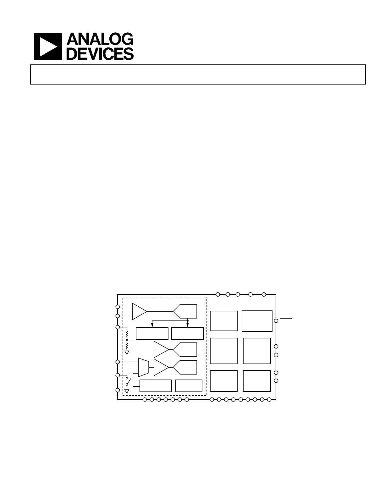
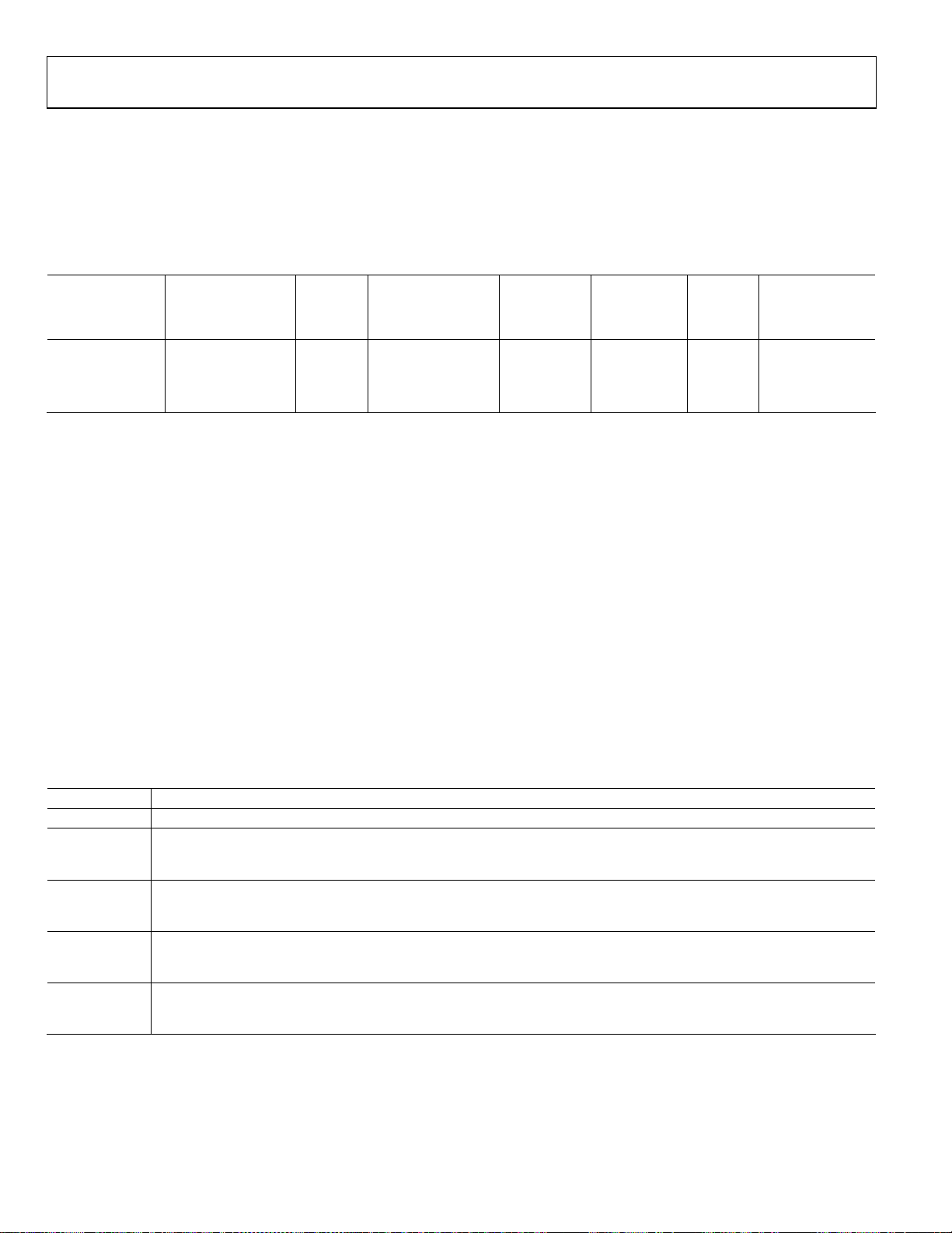
FUNCTIONAL BLOCK DIAGRAM
IIN+
IIN–
VBAT
VTEMP
GND_SW
VREF
Rev. A
Information furnished by Analog Devices is believed to be accurate and reliable. However, no
responsibility is assumed by Anal og Devices for its use, nor for any infringements of patents or ot her
rights of third parties that may result from its use. Specifications subject to change without notice. No
license is granted by implication or otherwise under any patent or patent rights of Analog Devices.
Trademarks and registered trademarks are the property of their respective owners.
PRECISION ANALOG ACQUI S ITION
PGA
RESULT
ACCUMULATOR
MUX
TEMPERATURE
SENSOR
VDD
REG_AVDD
BUF
BUF
REG_DVDD
16-BIT
Σ-∆ ADC
DIGITAL
COMPARATOR
16-BIT
Σ-∆ ADC
16-BIT
Σ-∆ ADC
PRECISION
REFERENCE
VSS
AGND
DGND
IO_VSS
Figure 1.
TDI TDO NTRST TMS
TC
ADuC7032-8L
2.6V LDO
PSM
POR
ARM7TDMI
MCU
20MHz
2× TIMERS
WDT
W/U TIMER
GPIO_0
GPIO_1
GPIO_2
One Technology Way, P.O. Box 9106, Norwood, MA 02062-9106, U.S.A.
Tel: 781.329.4700 www.analog.com
Fax: 781.461.3113 ©2007–2010 Analog Devices, Inc. All rights reserved.
128B ADC FIFO
®
LOW POWER
ON-CHIP PLL
GPIO_3
GPIO_4
MEMORY
96kB FLASH
6kB SRAM
PRECISION
OSC (1%)
OSC
GPIO PORT
UART PORT
SPI PORT
LIN
GPIO_5
GPIO_6
RESET
XTAL1
XTAL2
WU
LIN
GPIO_7
GPIO_8
05986-001

ADuC7032-8L
TABLE OF CONTENTS
Features.............................................................................................. 1
Applications....................................................................................... 1
Functional Block Diagram .............................................................. 1
Revision History ............................................................................... 3
Specifications..................................................................................... 4
Electrical Specifications............................................................... 4
Timing Specifications .................................................................. 9
Absolute Maximum Ratings.......................................................... 15
ESD Caution................................................................................ 15
Pin Configuration and Function Descriptions........................... 16
Terminology .................................................................................... 19
Theory of Operation ...................................................................... 20
Overview of the ARM7TDMI® Core ....................................... 20
Memory Organization ............................................................... 22
Reset .............................................................................................24
Flash/EE Memory and the ADuC7032-8L ............................. 25
Flash/EE Control Interface........................................................ 25
Flash/EE Memory Security ....................................................... 28
Flash/EE Memory Reliability.................................................... 31
Code Execution Time from SRAM and Flash/EE .....................31
ADuC7032-8L Kernel................................................................ 32
Memory Mapped Registers....................................................... 34
Complete MMR Listing............................................................. 35
16-Bit, Sigma-Delta Analog-to-Digital Converters ................... 39
Current Channel ADC (I-ADC) .............................................. 39
Voltage Channel ADC (V-ADC).............................................. 40
Temperature Channel ADC (T-ADC)..................................... 40
ADC Ground Switch.................................................................. 41
ADC Noise Performance Tables............................................... 42
ADC MMR Interface .................................................................43
ADC Power Modes of Operation............................................. 54
ADC Diagnostics........................................................................ 59
Power Supply Support Circuits..................................................... 60
ADuC7032-8L System Clocks ...................................................... 61
ADuC7032-8L Low Power Clock Calibration........................ 65
Processor Reference Peripherals................................................... 67
Interrupt System......................................................................... 67
Timers .............................................................................................. 69
Synchronization of Timers Across Asynchronous Clock
Domains ...................................................................................... 70
Programming the Timers.......................................................... 71
Timer0—Lifetime Timer........................................................... 71
Timer1.......................................................................................... 73
Timer2—Wake-Up Timer......................................................... 75
Timer3—Watchdog Timer........................................................ 77
General-Purpose I/O ..................................................................... 79
High Voltage Peripheral Control Interface................................. 89
WU (Wake-Up) Pin ................................................................... 95
Handling Interrupts from the High Voltage Peripheral
Control Interface ........................................................................ 96
Low Voltage Flag (LVF)............................................................. 96
High Voltage Diagnostics .......................................................... 96
UART Serial Interface.................................................................... 97
Baud Rate Generation................................................................ 97
UART Register Definitions....................................................... 97
Serial Peripheral Interface........................................................... 101
MISO (Master In, Slave Out Data I/O Pin) ..........................101
MOSI (Master Out, Slave In Pin)........................................... 101
SCLK (Serial Clock I/O Pin)................................................... 101
Chip Select (SS) Input Pin....................................................... 101
SPI Registers Definitions......................................................... 101
LIN (Local Interconnect Network) Interface............................ 104
LIN MMR Description............................................................ 104
LIN Hardware Interface .......................................................... 108
ADuC7032-8L On-Chip Diagnostics........................................ 112
ADC Diagnostics...................................................................... 112
High Voltage I/O Diagnostics................................................. 112
Part Identification......................................................................... 113
ADuC7032-8L Example Schematic ........................................... 116
Outline Dimensions..................................................................... 117
Ordering Guide ........................................................................ 117
Rev. A | Page 2 of 120

ADuC7032-8L
REVISION HISTORY
11/10—Rev. 0 to Rev. A
Changed ±4.68 mV to ±9.375 mV, Table 32................................42
Changes to Timers Section ............................................................69
Added Synchronization of Timers Across Asynchronous Clock
Domains Section .............................................................................70
Added Figure 32 and Figure 33; Renumbered Sequentially......70
Added Programming the Timers Section, Halting Timer2
Section, Starting Timer2 Section, and
Example Code Section....................................................................71
Updated Outline Dimensions......................................................117
Changes to Ordering Guide.........................................................117
8/07—Revision 0: Initial Version
Rev. A | Page 3 of 120

ADuC7032-8L
SPECIFICATIONS
ELECTRICAL SPECIFICATIONS
VDD = 3.5 V to 18 V, VREF = 1.2 V internal reference; f
precision oscillator. All specifications T
Table 1.
Parameter Test Conditions/Comments Min Typ Max Unit
ADC SPECIFICATIONS
Conversion Rate1
Chop off, ADC normal operating mode 4 8000 Hz
Chop on, ADC normal operating mode 4 2600 Hz
Chop on, ADC low power mode 1 650 Hz
Current Channel
No Missing Codes1 Valid for all ADC update rates and ADC modes 16 Bits
Integral Nonlinearity
Offset Error
Offset Error
Offset Error
Offset Error
Offset Error
1, 2 , 3, 4, 5
2, 3, 4, 6
1, 3, 6
1, 3
1, 3
Offset Error Drift6 Chop off, valid for ADC gains of 4 to 64, normal mode 0.03 LSB/°C
Offset Error Drift6 Chop off, valid for ADC gains of 128 to 512, normal mode 30 nV/°C
Offset Error Drift6 Chop on 10 nV/°C
Total Gain Error
Total Gain Error
Total Gain Error
Gain Drift 3 ppm/°C
PGA Gain Mismatch Error ±0.1 %
Output Noise
10 Hz update rate, gain = 512, chop enabled 100 150 nV rms
1 kHz update rate, gain = 512 0.6 0.9 μV rms
1 kHz update rate, gain = 32 0.8 1.2 μV rms
1 kHz update rate, gain = 4 2.0 2.8 μV rms
8 kHz update rate, gain = 32 2.5 3.5 μV rms
8 kHz update rate, gain = 4 14 21 μV rms
ADC low power mode, f
ADC low power mode, f
ADC low power plus mode, f
Voltage Channel12
No Missing Codes1 Valid at all ADC update rates 16 Bits
Integral Nonlinearity
Offset Error
Offset Error
1, 3, 5
1, 3
Offset Error Drift Chop off 0.03 LSB/°C
Total Gain Error
Total Gain Error
Gain Drift
Output Noise
10 Hz update rate 60 90 μV rms
1 kHz update rate 180 270 μV rms
8 kHz update rate 1600 2400 μV rms
1, 2
±10 ±60 ppm of FSR
Chop off, 1 LSB = (36.6/gain) μV, after initial offset calibration −10 ±3 +10 LSB
Chop off, 1 LSB = (36.6/gain) μV −15 +35 LSB
Chop on −2 ±0.5 +2 μV
Chop on, low power mode or low power plus mode, MCU powered
Chop on, normal mode, CD = 1 0 −1.5 −5 μV
1, 3, 7 , 8, 9
Normal mode −0.5 ±0.1 +0.5 %
1, 3, 7, 9, 10
1, 3, 7, 9
Low power plus mode, using precision VREF −1 ±0.2 +1 %
1, 11
4 Hz update rate, gain = 512, chop enabled 60 90 nV rms
1
Chop off, 1 LSB = 439.5 μV −10 ±1 +10 LSB
Chop on 0.3 1 LSB
1, 3, 7, 13, 14
1, 3, 7, 13, 14
1, 15
4 Hz update rate 60 90 μV rms
= 10.24 MHz, driven from external 32.768 kHz watch crystal or on-chip
CORE
= −40°C to +105°C, unless otherwise noted.
A
down 0 −200 −650 nV
Low power mode −4 ±0.2 +4 %
= 10 Hz, gain = 128 1.25 1.9 μV rms
ADC
= 1 Hz, gain = 128 0.35 0.5 μV rms
ADC
= 1 Hz, gain = 512 0.1 0.15 μV rms
ADC
±10 ±60 ppm of FSR
Includes resistor mismatch −0.25 ±0.06 +0.25 %
Temperature range = −25°C to +65°C −0.15 ±0.03 +0.15 %
Includes resistor mismatch drift 3 ppm/°C
Rev. A | Page 4 of 120

ADuC7032-8L
Parameter Test Conditions/Comments Min Typ Max Unit
Temperature Channel
No Missing Codes1 Valid at all ADC update rates 16 Bits
Integral Nonlinearity
Offset Error
Offset Error
1, 3, 5, 16, 17, 18
1, 3
Offset Error Drift
Total Gain Error
Gain Drift
Output Noise
ADC SPECIFICATIONS,
ANALOG INPUT
Current Channel
Absolute Input Voltage
Range
Input Voltage Range
Gain = 221 ±600 mV
Gain = 421 ±300 mV
Gain = 8 ±150 mV
Gain = 16 ±75 mV
Gain = 32 ±37.5 mV
Gain = 64 ±18.75 mV
Gain = 128 ±9.375 mV
Gain = 256 ±4.68 mV
Gain = 512 ±2.3 mV
Input Leakage Current
Input Offset Current
Voltage Channel
Absolute Input Voltage
Range
Input Voltage Range 0 to 28.8 V
VBAT Input Current VBAT = 18 V 3 5.5 8 μA
Temperature Channel
Absolute Input Voltage
Range
Input Voltage Range 0 to VREF V
VTEMP Input Current1 2.5 100 nA
VOLTAGE REFERENCE
ADC Precision Reference
Internal VREF 1.2 V
Power-Up Time1 0.5 ms
Initial Accuracy1 Measured at TA = 35°C −0.15 +0.15 %
Internal VREF Temperature
Coefficient
Long-Term Stability24 100 ppm/
External Reference Input
Range
25
VREF Divide-by-2 Initial Error1 0.1 0.3 %
ADC Low Power Reference
Internal VREF
Initial Accuracy
Initial Accuracy10 Using ADCREF, measured at TA = 35°C 0.1 %
Temperature Coefficient
RESISTIVE ATTENUATOR
Divider Ratio 24
Resistor Mismatch Drift 3 ppm/°C
ADC GROUND SWITCH
Resistance Direct path to ground 10 Ω
20 kΩ resistor selected 10 20 30 kΩ
Input Current 6 mA
1
±10 ±60 ppm of FSR
Chop off, 1 LSB = 19.84 μV −10 ±3 +10 LSB
Chop on −5 1 +5 LSB
1, 3, 14, 17, 18
0.03 LSB/°C
−0.25 ±0.06 +0.25 %
3 ppm/°C
1
1 kHz update rate 7.5 11.25 μV rms
Internal VREF = 1.2 V
Applies to both IIN+ and IIN− −200 +300 mV
19, 20
1, 22
Gain = 121 ±1.2 V
1
−3 +3 nA
0.5 1.5 nA
4 18 V
100 1300 mV
1, 23
−20 ±5 +20 ppm/°C
1000 hr
0.1 1.3 V
1.2 V
Measured at TA = 35°C −5 +5 %
1, 23
−300 +300 ppm/°C
Rev. A | Page 5 of 120

ADuC7032-8L
Parameter Test Conditions/Comments Min Typ Max Unit
TEMPERATURE SENSOR
Accuracy MCU in power-down or standby mode;
POWER-ON RESET (POR)
POR Trip Level Refers to voltage at VDD pin 2.85 3.0 3.15 V
POR Hysteresis 300 mV
Reset Timeout from POR 20 ms
LOW VOLTAGE FLAG (LVF)
LVF Level Refers to voltage at VDD pin 1.9 2.1 2.3 V
POWER SUPPLY MONITOR (PSM)
PSM Trip Level Refers to voltage at VDD pin 6.0 V
WATCHDOG TIMER (WDT)
Timeout Period
Timeout Step Size 7.8 ms
FLASH/EE MEMORY
Endurance27 10,000 Cycles
Data Retention28 20 Years
DIGITAL INPUTS All digital inputs except NTRST
Input Leakage Current Input (high) = REG_DVDD −10 ±1 +10 μA
Input Pull-Up Current
Input Capacitance
Input Leakage Current NTRST only: input (low) = 0 V −10 ±1 +10 μA
Input Pull-Down Current NTRST only: input (high) = REG_DVDD 30 55 100 μA
LOGIC INPUTS
1
Input Low Voltage (VINL) 0.4 V
Input High Voltage (VINH) 2.0 V
CRYSTAL OSCILLATOR
Logic Inputs, XTAL1 Only
Input Low Voltage (VINL) 0.8 V
Input High Voltage (VINH) 1.7 V
XTAL1 Capacitance 12 pF
XTAL2 Capacitance 12 pF
ON-CHIP OSCILLATORS
Low Power Oscillator 131.072 kHz
Accuracy29 Includes drift data from 1000 hr life test −3 +3 %
Precision Oscillator 131.072 kHz
Accuracy Includes drift data from 1000 hr life test −1 +1 %
MCU CLOCK RATE Eight programmable core clock selections within this range (binary
MCU START-UP TIME
At Power-On Includes kernel power-on execution time 25 ms
After Reset Event Includes kernel power-on execution time 5 ms
From MCU Power-Down
Oscillator Running
Wake-Up from Interrupt 2 ms
Wake-Up from LIN 2 ms
Crystal Powered Down
Wake-Up from Interrupt 500 ms
Internal PLL Lock Time 1 ms
1, 26
−4 +4 °C
temperature range = −40°C to −30°C
MCU in power-down or standby mode;
−3 +3 °C
temperature range = −30°C to −16°C
MCU in power-down or standby mode;
−2 +2 °C
temperature range = −16°C to +40°C
MCU in power-down or standby mode;
−4 +4 °C
temperature range = +40°C to +70°C
MCU in power-down or standby mode;
−8 +8 °C
temperature range = +70°C to +85°C
MCU in power-down or standby mode;
−12 +12 °C
temperature range = +85°C to +105°C
1
1
32.768 kHz clock, 256 prescale 0.008 512 sec
Input (low) = 0 V −80 −20 −10 μA
10 pF
All logic inputs
1
0.160 10.24 20.48 MHz
divisions 1, 2, 4, 8. . .64, 128)
Rev. A | Page 6 of 120

ADuC7032-8L
Parameter Test Conditions/Comments Min Typ Max Unit
LIN I/O GENERAL
Baud Rate 1000 20,000 Bits/sec
VDD Supply voltage range at which the LIN interface is functional 7 18 V
Input Capacitance 5.5 pF
LIN Comparator Response
1
Time
I
LIN DOM MAX
I
LIN_PAS_REC
I
LIN_PAS_DOM1
I
LIN_NO_GND
V
V
V
V
V
Driver off; 7.0 V < V
30
LIN_DOM1
LIN_REC1
1
LIN receiver center voltage, VDD > 7.0 V 0.475 VDD 0.5 VDD 0.525 VDD V
LIN_CNT
1
LIN receiver hysteresis voltage 0.175 VDD V
HYS
LIN_DOM_DRV_LOSUP1
RL 500 Ω 1.2 V
RL 1000 Ω 0.6 V
V
LIN_DOM_DRV_HISUP
1
LIN dominant output voltage; VDD = 18 V
RL 500 Ω 2 V
RL 1000 Ω 0.8 V
V
LIN_RECESSIVE
LIN recessive output voltage 0.8 VDD V
VBAT Shift30 0 0.1 VDD V
GND Shift
R
V
30
Slave termination resistance 20 29 47 kΩ
SLAVE
30
SERIAL DIODE
Voltage drop at the serial diode, D
Transmit Propagation Delay1 V
Symmetry of Transmit
Propagation Delay1 V
Receive Propagation Delay1
Symmetry of Receive
Propagation Delay1 V
LIN v.1.3 SPECIFICATION
1
dV
dt
1
dV
dt
t
SYM1
Symmetry of rising and falling edge, VBAT = 7 V −4 +4 μs
LIN 2.0 SPECIFICATION
D1 Duty Cycle 1 0.396
TH
TH
V
D1 = t
D2 Duty Cycle 2
TH
TH
V
D2 = t
Using 22 Ω resistor 38 90 μs
Current limit for driver when LIN bus is in dominant state;
40 200 mA
VBAT = VBAT(MAX)
< 18 V; VDD = V
BUS
Input leakage V
= 0 V −1 mA
LIN
Control unit disconnected from ground,
GND = VDD; 0 V < V
< 18 V; VBAT = 12 V
LIN
− 0.7 V −20 +20 μA
LIN
−1 +1 mA
LIN receiver dominant state, VDD > 7.0 V 0.4 VDD V
LIN receiver recessive state, VDD > 7.0 V 0.6 VDD V
LIN dominant output voltage; VDD = 7.0 V
0 0.1 VDD V
Ser_Int
= 7 V 4 μs
DDMIN
Bus load conditions (C
BUS
||R
BUS
):
0.4 0.7 1 V
1 nF||1 kΩ; 6.8 nF||660 Ω; 10 nF||500 Ω
= 7 V −2 +2 μs
DDMIN
V
= 7 V
DDMIN
= 7 V −2 +2 μs
DDMIN
||R
Bus load conditions (C
BUS
BUS
):
6 μs
1 nF||1 kΩ ; 6.8 nF||660 Ω; 10 nF||500 Ω
Slew rate
Dominant and recessive edges, VBAT = 18 V 1 2 3 V/μs
Slew rate
Dominant and recessive edges, VBAT = 7 V 0.5 3 V/μs
Symmetry of rising and falling edge, VBAT = 18 V −5 +5 μs
||R
Bus load conditions ( C
BUS
BUS
):
1 nF||1 kΩ; 6.8 nF||660 Ω; 10 nF||500 Ω
= 0.744 × VBAT,
REC(MAX)
= 0.581 × VBAT,
DOM(MAX)
= 7.0 V…18 V; t
SUP
BUS_REC(MIN)
REC(MIN)
DOM(MIN)
= 7.0 V…18 V; t
SUP
BUS_REC(MAX)
/(2 × t
= 0.284 × VBAT,
= 0.422 × VBAT,
/(2 × t
= 50 μs,
BIT
)
BIT
= 50 μs,
BIT
) 0.581
BIT
Rev. A | Page 7 of 120

ADuC7032-8L
Parameter Test Conditions/Comments Min Typ Max Unit
PACKAGE THERMAL
SPECIFICATIONS
Thermal Shutdown31 140 150 160 °C
Thermal Impedance (θJA)32
Top die 50 °C/W
POWER REQUIREMENTS
Power Supply Voltages
VDD (Battery Supply) 3.5 18 V
REG_DVDD, REG_AVDD33 2.5 2.6 2.7 V
Power Consumption
IDD (MCU Normal Mode)34 MCU clock rate = 10.24 MHz, ADC off 10 20 mA
MCU clock rate = 20.48 MHz, ADC off 20 30 mA
IDD (MCU Powered Down)1 ADC low power mode, measured over an ambient temperature range
ADC low power mode, measured over an ambient temperature range
Average current, measured with wake-up and watchdog timer
Average current, measured with wake-up and watchdog timer clocked
IDD (Current ADC) 1.7 mA
IDD (Voltage/Temperature
ADC)
IDD (Precision Oscillator) 400 μA
1
Not guaranteed by production test, but by design and/or characterization data at production release.
2
Valid for current ADC gain setting of PGA = 4 to 64.
3
These numbers include temperature drift.
4
Tested at gain range = 4; self-offset calibration removes this error.
5
Measured with an internal short after an initial offset calibration.
6
Measured with an internal short.
7
Includes internal reference temperature drift.
8
Factory calibrated at gain = 1.
9
System calibration at specific gain range removes the error at this gain range at that temperature.
10
Valid when used in conjunction with the ADCREF (the low power mode reference error) MMR.
11
Typical noise in low power modes is measured with chop enabled.
12
Voltage channel specifications include resistive attenuator input stage.
13
Includes an initial system calibration.
14
System calibration removes this error at that temperature.
15
RMS noise is referred to voltage attenuator input. For example, at f
yields these input referred noise figures.
16
ADC self-offset calibration removes this error.
17
Valid after an initial self-calibration.
18
Factory calibrated for the internal temperature sensor during final production test.
19
In ADC low power mode, the input range is fixed at ±9.375 mV. In ADC low power plus mode, the input range is fixed at ±2.34375 mV.
20
It is possible to extend the ADC input range by up to 10% by modifying the factory set value of the gain calibration register or using system calibration. This approach
can also be used to reduce the ADC input range (LSB size).
21
Limited by minimum/maximum absolute input voltage range.
22
Valid for a differential input less than 10 mV.
23
Measured using box method.
24
The long-term stability specification is noncumulative. The drift in subsequent 1000 hour periods is significantly lower than in the first 1000 hour period.
25
References of up to REG_AVDD can be accommodated by enabling an internal divide-by-2.
26
Die temperature.
27
Endurance is qualified to 10,000 cycles, as per JEDEC Std. 22 Method A117, and measured at −40°C, +25°C, and +125°C. Typical endurance at 25°C is 170,000 cycles.
28
Retention lifetime equivalent at junction temperature (TJ) = 85°C, as per JEDEC Std. 22 Method A117. Retention lifetime derates with junction temperature.
29
Low power oscillator can be calibrated against either the precision oscillator or the external 32.768 kHz crystal in user code.
30
These numbers are not production tested but are supported by LIN compliance testing.
31
The MCU core is not shut down, but an interrupt is generated, if enabled.
32
Thermal impedance can be used to calculate the thermal gradient from ambient to die temperature.
33
Internal regulated supply available at REG_DVDD (I
34
Typical additional supply current consumed during Flash/EE memory program and erase cycles is 7 mA and 5 mA, respectively.
48-lead LQFP, stacked die
Bottom die 25 °C/W
300 400 μA
of −10°C to +40°C (continuous ADC c onversion)
300 500 μA
of −40°C to +85°C (continuous ADC c onversion)
ADC low power plus mode, measured over an ambient temperature
520 700 μA
range of −10°C to +40°C (continuous ADC conversion)
120 300 μA
clocked from low power oscillator (−40°C to +85°C)
120 175 μA
from low power oscillator over an ambient temperature range of −10°C
to +40°C
Per ADC 0.5 mA
= 1 kHz, typical rms noise at the ADC input is 7.5 μV, which, when scaled by the attenuator (24),
ADC
= 5 mA) and REG_AVDD (I
SOURCE
SOURCE
= 1 mA).
Rev. A | Page 8 of 120
ADuC7032-8L
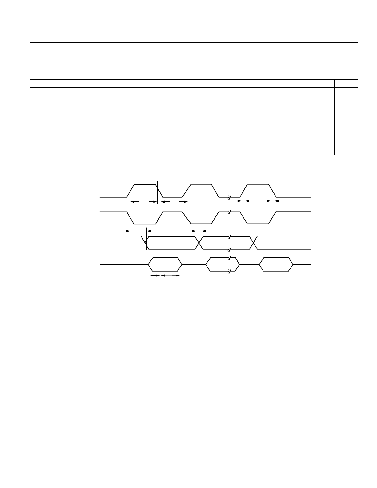
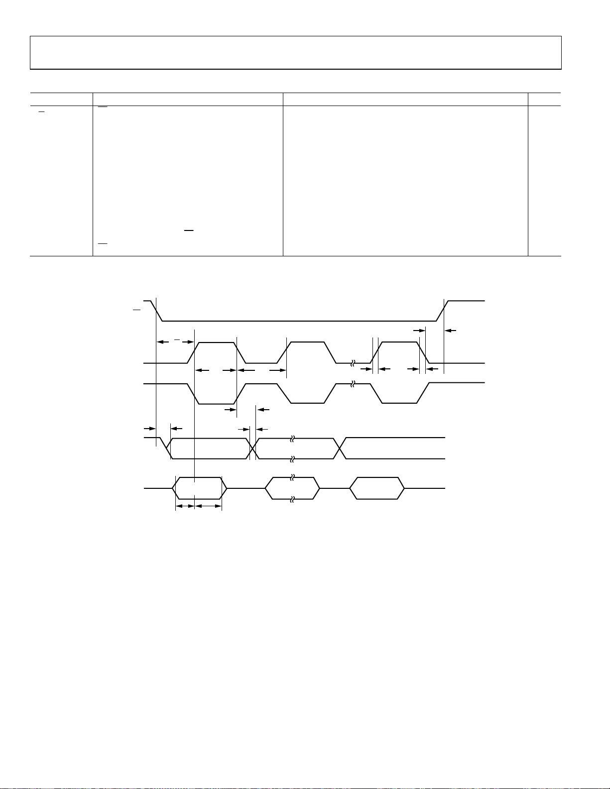
TIMING SPECIFICATIONS
SPI Timing Specifications
Table 2. SPI Master Mode Timing (PHASE Mode = 1)
Parameter Description Min Typ Max Unit
tSL SCLK low pulse width1 (SPIDIV + 1) × t
tSH SCLK high pulse width1 (SPIDIV + 1) × t
t
Data output valid after SCLK edge2 (2 × t
DAV
t
Data input setup time before SCLK edge 0 ns
DSU
t
Data input hold time after SCLK edge2 3 × t
DHD
ns
UCLK
tDF Data output fall time 3.5 ns
tDR Data output rise time 3.5 ns
tSR SCLK rise time 3.5 ns
tSF SCLK fall time 3.5 ns
1
t
depends on the clock divider or CD bits in PLLCON MMR. t
HCLK
2
t
= 48.8 ns. It corresponds to the 20.48 MHz internal clock from the PLL before the clock divider.
UCLK
HCLK
= t
UCLK
/2CD.
SCLK
(POLARITY = 0)
SCLK
(POLARITY = 1)
t
SH
t
DAV
t
SL
t
DF
t
DR
t
SR
ns
HCLK
ns
HCLK
) + (2 × t
UCLK
t
SF
) ns
HCLK
MOSI
MISO
MSB IN BITS[6:1] LSB IN
t
DSUtDHD
Figure 2. SPI Master Mode Timing (PHASE Mode = 1)
LSBBITS[6:1]MSB
05986-002
Rev. A | Page 9 of 120
ADuC7032-8L
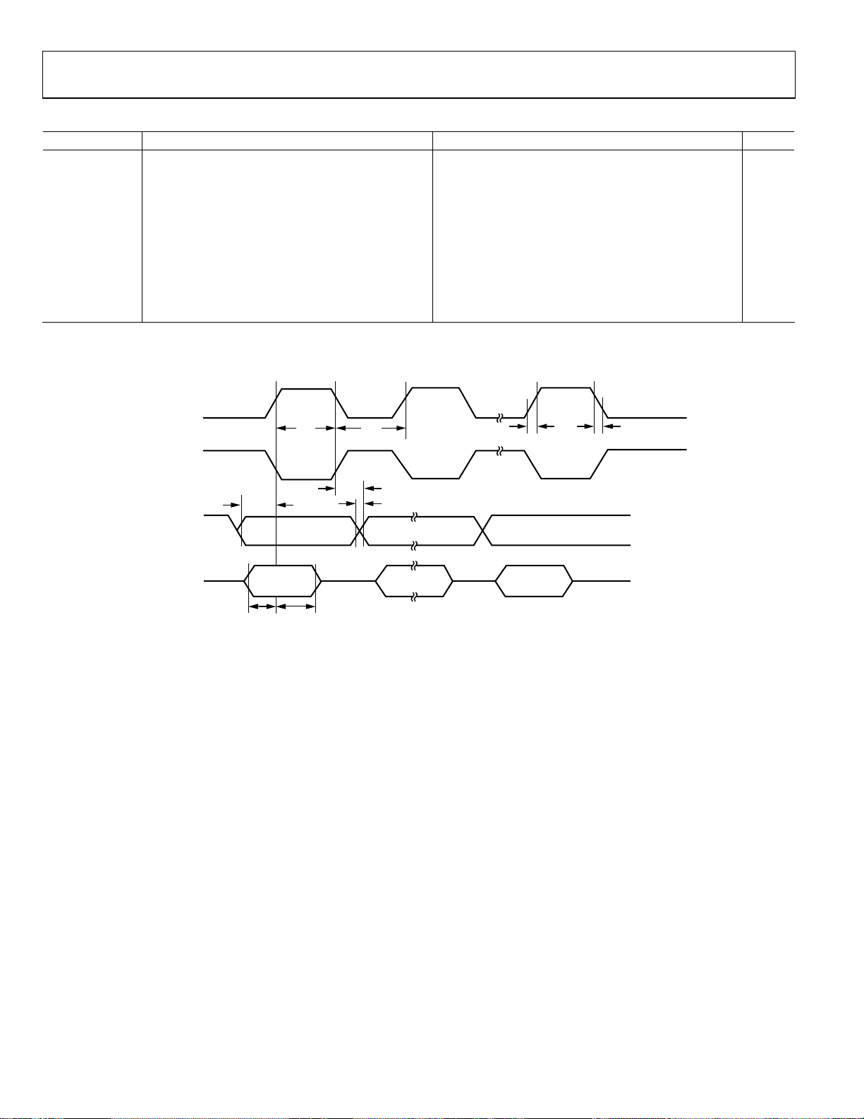
Table 3. SPI Master Mode Timing (PHASE Mode = 0)
Parameter Description Min Typ Max Unit
tSL SCLK low pulse width1 (SPIDIV + 1) × t
tSH SCLK high pulse width1 (SPIDIV + 1) × t
t
Data output valid after SCLK edge2 (2 × t
DAV
t
Data output setup time before SCLK edge ½ tSL ns
DOSU
t
Data input setup time before SCLK edge 0 ns
DSU
t
Data input hold time after SCLK edge2 3 × t
DHD
ns
UCLK
tDF Data output fall time 3.5 ns
tDR Data output rise time 3.5 ns
tSR SCLK rise time 3.5 ns
tSF SCLK fall time 3.5 ns
1
t
depends on the clock divider or CD bits in PLLCON MMR. t
HCLK
2
t
= 48.8 ns. It corresponds to the 20.48 MHz internal clock from the PLL before the clock divider.
UCLK
HCLK
= t
UCLK
/2CD.
SCLK
(POLARITY = 0)
SCLK
(POLARITY = 1)
t
DOSU
t
SH
t
t
SL
t
DAV
DF
t
DR
t
SR
ns
HCLK
ns
HCLK
) + (2 × t
UCLK
t
SF
) ns
HCLK
MOSI
MISO
MSB IN BITS[6:1] LSB IN
t
DSUtDHD
Figure 3. SPI Master Mode Timing (PHASE Mode = 0)
LSBBITS[6:1]MSB
5986-003
Rev. A | Page 10 of 120
ADuC7032-8L
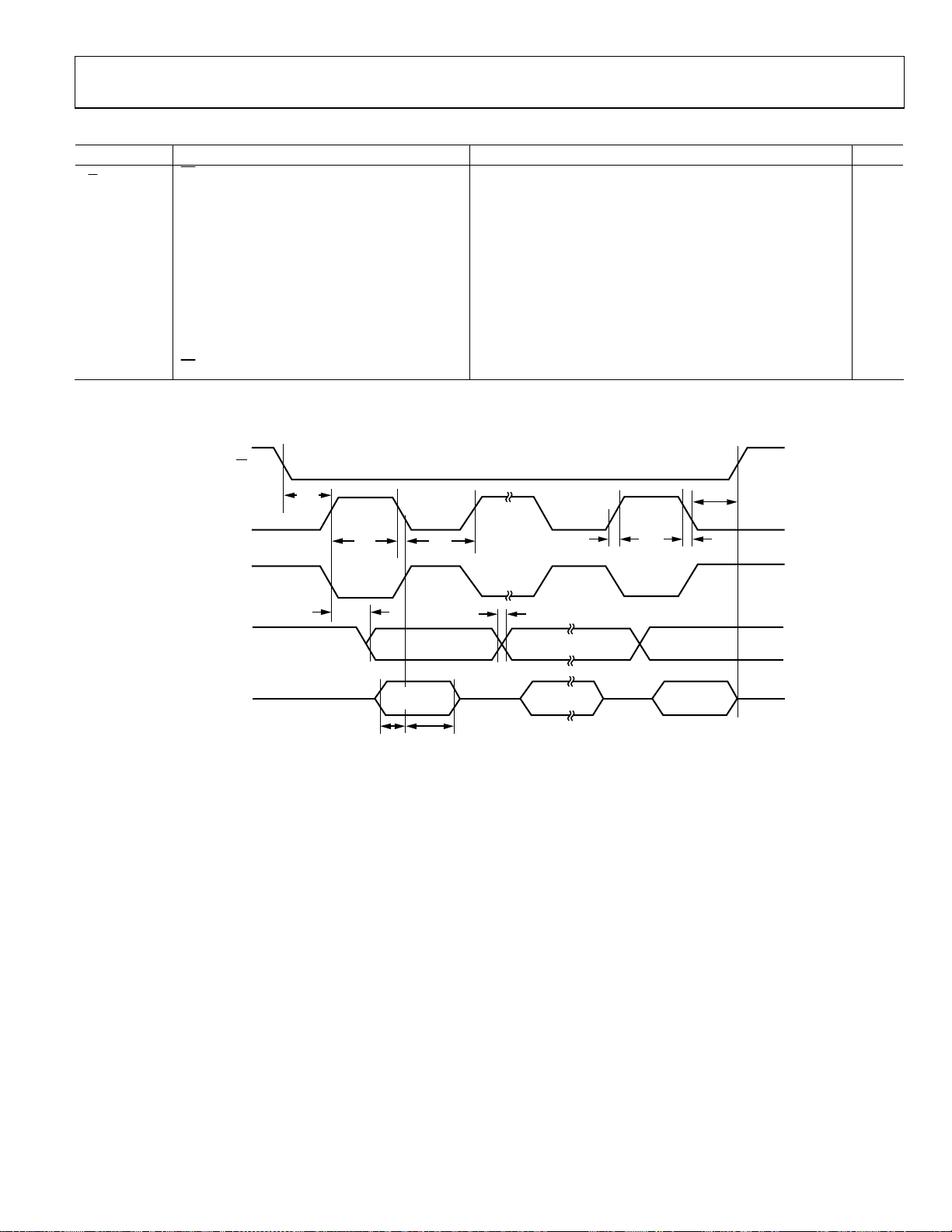
Table 4. SPI Slave Mode Timing (PHASE Mode = 1)
Parameter Description Min Typ Max Unit
tSS
to SCLK edge
SS
tSL SCLK low pulse width1 (SPIDIV + 1) × t
tSH SCLK high pulse width1 (SPIDIV + 1) × t
t
Data output valid after SCLK edge2 (3 × t
DAV
t
Data input setup time before SCLK edge 0 ns
DSU
t
Data input hold time after SCLK edge2 4 × t
DHD
tDF Data output fall time 3.5 ns
tDR Data output rise time 3.5 ns
tSR SCLK rise time 3.5 ns
tSF SCLK fall time 3.5 ns
t
SFS
1
t
depends on the clock divider or CD bits in PLLCON MMR. t
HCLK
2
t
= 48.8 ns. It corresponds to the 20.48 MHz internal clock from the PLL before the clock divider.
UCLK
high after SCLK edge
SS
HCLK
= t
UCLK
SS
½ t
½ t
/2CD.
ns
SL
ns
HCLK
ns
HCLK
) + (2 × t
UCLK
ns
UCLK
ns
SL
) ns
HCLK
SCLK
(POLARITY = 0)
SCLK
(POLARITY = 1)
MISO
MOSI
t
CS
t
SH
t
DAV
t
DSUtDHD
t
SL
t
DF
MSB IN BITS[6:1] LSB IN
t
DR
t
SR
t
SFS
t
SF
LSBBITS[6:1]MSB
05986-004
Figure 4. SPI Slave Mode Timing (PHASE Mode = 1)
Rev. A | Page 11 of 120
ADuC7032-8L
Table 5. SPI Slave Mode Timing (PHASE Mode = 0)
Parameter Description Min Typ Max Unit
tSS
to SCLK edge
SS
tSL SCLK low pulse width1 (SPIDIV + 1) × t
tSH SCLK high pulse width1 (SPIDIV + 1) × t
t
Data output valid after SCLK edge2 (3 × t
DAV
t
Data input setup time before SCLK edge 0 ns
DSU
t
Data input hold time after SCLK edge2 4 × t
DHD
tDF Data output fall time 3.5 ns
tDR Data output rise time 3.5 ns
tSR SCLK rise time 3.5 ns
tSF SCLK fall time 3.5 ns
t
DOCS
t
SFS
1
t
depends on the clock divider or CD bits in PLLCON MMR. t
HCLK
2
t
= 48.8 ns. It corresponds to the 20.48 MHz internal clock from the PLL before the clock divider.
UCLK
Data output valid after SS
high after SCLK edge
SS
edge2
HCLK
= t
UCLK
SS
t
t
DOCS
SS
t
SH
t
DAV
t
DF
SCLK
(POLARITY = 0)
SCLK
(POLARITY = 1)
½ t
ns
UCLK
ns
SL
(3 × t
t
/2CD.
SL
t
DR
½ t
ns
SL
t
SR
ns
HCLK
ns
HCLK
) + (2 × t
UCLK
) + (2 × t
UCLK
t
SFS
t
SF
) ns
HCLK
) ns
HCLK
MISO
MOSI
MSB IN BITS[6:1] LSB IN
t
DSUtDHD
Figure 5. SPI Slave Mode Timing (PHASE Mode = 0)
LSBBITS[6:1]MSB
05986-005
Rev. A | Page 12 of 120
ADuC7032-8L
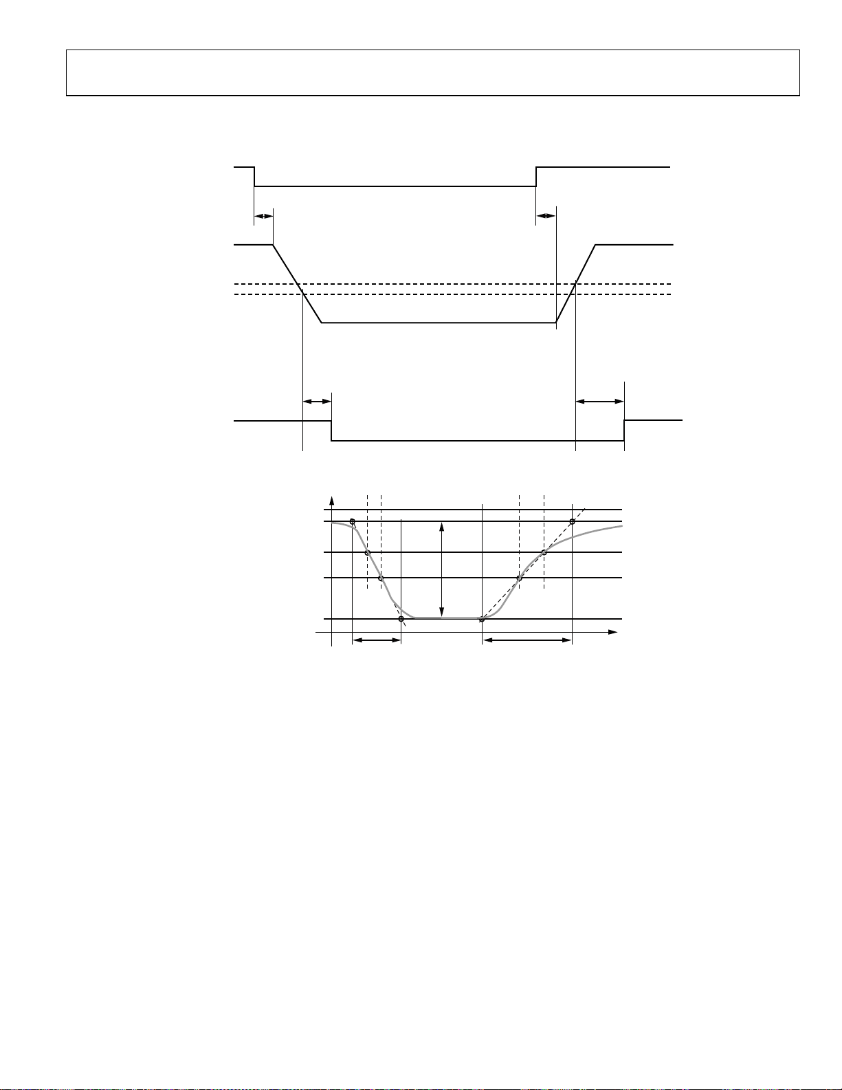
LIN Timing Specifications
TxD (INPUT TO TRANSCEIVE R FRO M CO NT RO L L ER)
RECEIVING
THRESHOLD
t
TRANS_PDF
BUS SIGNAL
t
RxD (OUTPUT OF TRANSCEI VE R TO CONTROLLER)
V
SUP
V
BUSREC
60%
40%
V
BUSDOM
GND
(MEASURED FROM POINT WHEN THE
REC_PDF
SWITCHING THRESHOLD IS SURPASSED)
t
FALL_60%
t
SLOPE_FALL
t
FALL_40%
Figure 6. LIN v.1.3 Timing Specifications
V
SWING
t
RISE_40%
t
t
SLOPE_RISE
t
RISE_60%
TRANS_PDR
t
REC_PDR
TIME
05986-006
Rev. A | Page 13 of 120
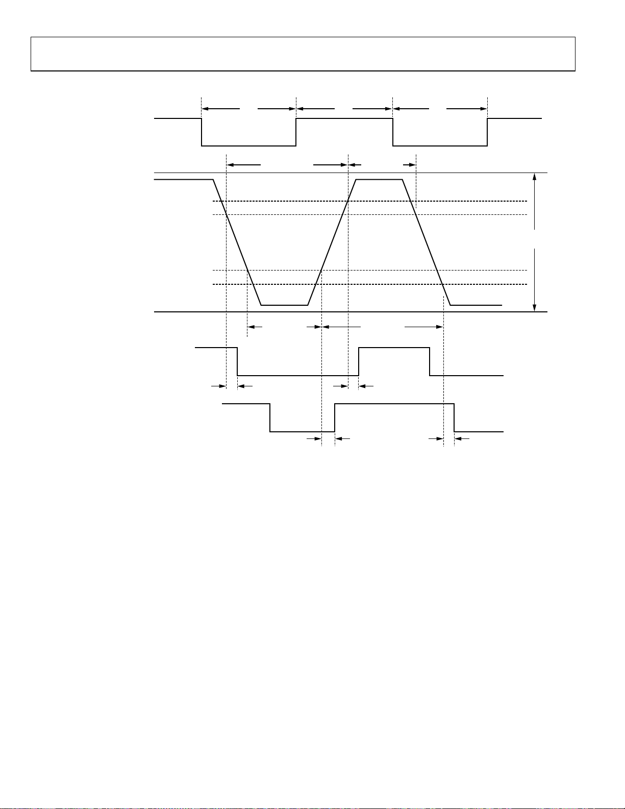
ADuC7032-8L
TRANSMIT
INPUT TO
TRANSMITTING
NODE
V
(TRANSCEIVER SUP PL Y
OF T R AN SMITTING NODE)
SUP
RxD
(OUTPUT OF RECEIV ING NODE 1)
RECESSIVE
DOMINANT
TH
REC (MAX)
TH
DOM (MAX)
TH
REC (MIN)
TH
DOM (MIN)
t
BIT
t
LIN_DO M (MAX)
t
LIN_DO M (MIN)
t
RX_PDF
t
BIT
t
LIN_REC ( MIN)
t
LIN_REC (MAX)
t
RX_PDR
t
BIT
THRESHOLDS OF
RECEIVING NODE 1
THRESHOLDS OF
RECEIVING NODE 2
LIN
BUS
(OUTPUT OF RECEIV ING NODE 2)
RxD
t
RX_PDR
Figure 7. LIN 2.0 Timing Specifications
t
RX_PDF
05986-007
Rev. A | Page 14 of 120
ADuC7032-8L
ABSOLUTE MAXIMUM RATINGS
= −40°C to +105°C, unless otherwise noted.
T
A
Table 6.
Parameter Rating
AGND to DGND to VSS to IO_VSS −0.3 V to +0.3 V
VBAT to AGND −22 V to +40 V
VDD to VSS −0.3 V to +33 V
VDD to VSS for 1 sec −0.3 V to +40 V
LIN to IO_VSS −16 V to +40 V
WU to IO_VSS −3 V to +33 V
WU Continuous Current 50 mA
High Voltage I/O Pins Short-Circuit
Current
Digital I/O Voltage to DGND −0.3 V to REG_DVDD + 0.3 V
VREF to AGND −0.3 V to REG_AVDD + 0.3 V
ADC Inputs to AGND −0.3 V to REG_AVDD + 0.3 V
Storage Temperature 130°C
Junction Temperature (Transient) 150°C
Junction Temperature (Continuous) 130°C
Lead Temperature
Soldering Reflow (15 sec) 260°C
100 mA
Stresses above those listed under Absolute Maximum Ratings
may cause permanent damage to the device. This is a stress
rating only; functional operation of the device at these or any
other conditions above those indicated in the operational
section of this specification is not implied. Exposure to absolute
maximum rating conditions for extended periods may affect
device reliability.
ESD CAUTION
Rev. A | Page 15 of 120

ADuC7032-8L
PIN CONFIGURATION AND FUNCTION DESCRIPTIONS
LIN
IO_VSS
RESERVEDNCVSSNCVDDWUNCNCNC
4847464544434241403938
XTAL2
37
RESET
GPIO_5/IRQ1/RxD
GPIO_6/TxD
GPIO_7/IRQ4
GPIO_8/IRQ5
TCK
TDI
DGND
NC
TDO
NTRST
TMS
1
2
3
4
5
6
7
8
9
10
11
12
NC = NO CONNECT
PIN 1
IDENTIFIER
1314151617181920212223
VREF
VBAT
Table 7. Pin Function Descriptions
Pin No. Mnemonic Type1 Description
1
RESET
I
Reset Input Pin, Active Low. This pin has an internal, weak, pull-up resistor to REG_DVDD. When
not in use, this pin remains unconnected. For added security and robustness, it is recommended
that this pin be strapped, via a resistor, to REG_DVDD.
2 GPIO_5/IRQ1/RxD I/O
General-Purpose Digital Input/Output 5, External Interrupt Request 1, or Receive Data. By default
and after power-on reset, this pin is configured as an input. The pin has an internal, weak, pull-up
resistor and, when not in use, it can be left unconnected. This multifunction pin can be configured
in one of three states, namely
General-Purpose Digital I/O 5.
External Interrupt Request 1, active high.
Receive data for UART serial port.
This pin can also be used as a clock input to Timer1.
3 GPIO_6/TxD I/O
General-Purpose Digital Input/Output 6 or Transmit Data. By default and after power-on reset, this
pin is configured as an input. The pin has an internal, weak, pull-up resistor and, when not in use,
it can be left unconnected. This multifunction pin can be configured in one of two states, namely
General-Purpose Digital I/O 6.
Transmit data for UART serial port.
4 GPIO_7/IRQ4 I/O
General-Purpose Digital Input/Output 7 or External Interrupt Request 4. By default and after
power-on reset, this pin is configured as an input. The pin has an internal, weak, pull-up resistor and,
when not in use, it can be left unconnected. This multifunction pin can be configured in one of
two states, namely
General-Purpose Digital I/O 7.
External Interrupt Request 4, active high.
5 GPIO_8/IRQ5 I/O
General-Purpose Digital Input/Output 8 or External Interrupt Request 5. By default and after
power-on reset, this pin is configured as an input. The pin has an internal, weak, pull-up resistor
and, when not in use, it can be left unconnected. This multifunction pin can be configured in
one of two states, namely
General-Purpose Digital I/O 8.
External Interrupt Request 5, active high.
This pin can also be used as a clock input to Timer1.
ADuC7032-8L
TOP VIEW
(Not to S cale)
NC
NC
GND_SW
IIN–
IIN+
VTEMP
AGND
Figure 8. Pin Configuration
AGND
NC
24
REG_AVDD
36
XTAL1
35
DGND
34
DGND
33
REG_DVDD
32
NC
31
GPIO_4/ECLK
30
GPIO_3/MOSI
29
GPIO_2/MISO
28
GPIO_1/SCLK
27
GPIO_0/IRQ0/SS
26
NC
25
NC
05986-008
Rev. A | Page 16 of 120

ADuC7032-8L
Pin No. Mnemonic Type1 Description
6 TCK I
7 TDI I
8, 34, 35 DGND S Ground Reference for On-Chip Digital Circuits.
9, 16, 17,
23, 25, 26,
32, 38, 39,
40, 43, 45
10 TDO O
11 NTRST I
12 TMS I
13 VBAT I Battery Voltage Input to Resistor Divider.
14 VREF I
15 GND_SW S
18 VTEMP I External Pin for NTC/PTC Temperature Measurement.
19 IIN+ I Positive Differential Input for Current Channel.
20 IIN− I Negative Differential Input for Current Channel.
21, 22 AGND S Ground Reference for On-Chip Precision Analog Circuits.
24 REG_AVDD S Nominal 2.6 V Output from On-Chip Regulator.
27
28 GPIO_1/SCLK I/O
29 GPIO_2/MIS0 I/O
30 GPIO_3/MOSI I/O
31 GPIO_4/ECLK I/O
33 REG_DVDD S Nominal 2.6 V Output from the On-Chip Regulator.
NC
I/O
GPIO_0/IRQ0/SS
JTAG Test Clock. This clock input pin is one of the standard 5-pin JTAG debug ports on the part.
It is an input pin only, and it has an internal, weak, pull-up resistor. When not in use, this pin
remains unconnected.
JTAG Test Data Input. This data input pin is one of the standard 5-pin JTAG debug ports on the
part. It is an input pin only, and it has an internal, weak, pull-up resistor. When not in use, this pin
remains unconnected.
No Connect. This pin is not connected internally but is reserved for possible future use. Therefore,
this pin should not be connected externally. NC pins can be grounded, if required.
JTAG Test Data Output. This data output pin is one of the standard 5-pin JTAG debug ports on
the part. It is an output pin only. At power-on, this output is disabled and pulled high via an
internal, weak, pull-up resistor. When not in use, this pin remains unconnected.
JTAG Test Reset. This reset input pin is one of the standard 5-pin JTAG debug ports on the part.
It is an input pin only, and it has an internal, weak, pull-down resistor. When not in use, this pin
remains unconnected. It is also monitored by the on-chip kernel to enable LIN boot load mode.
JTAG Test Mode Select. This mode select input pin is one of the standard 5-pin JTAG debug ports
on the part. It is an input pin only, and it has an internal, weak, pull-up resistor. When not in use,
this pin remains unconnected.
External Reference Input Terminal. If this input is not used, connect it directly to the AGND
system ground.
Switch to Internal Analog Ground Reference. Negative input for external temperature channel
and external reference. If this input is not used, connect it directly to the AGND system ground.
General-Purpose Digital I/O 0, External Interrupt Request 0, or SPI Interface. By default and after
power-on reset, this pin is configured as an input. The pin has an internal, weak, pull-up resistor
and, when not in use, it remains unconnected. This multifunction pin can be configured in one
of three states, namely
General-Purpose Digital I/O 0.
External Interrupt Request 0, active high.
SPI interface, slave select input.
General-Purpose Digital I/O 1 or SPI Interface. By default and after power-on reset, this pin is
configured as an input. The pin has an internal, weak, pull-up resistor and, when not in use, it
remains unconnected. This multifunction pin can be configured in one of two states, namely
General-Purpose Digital I/O 1.
SPI interface, serial clock input.
General-Purpose Digital I/O 2 or SPI Interface. By default and after power-on reset, this pin is
configured as an input. The pin has an internal, weak, pull-up resistor and, when not in use, it
remains unconnected.This multifunction pin can be configured in one of two states, namely
General-Purpose Digital I/O 2.
SPI interface, master input/slave output pin.
General-Purpose Digital I/O 3 or SPI Interface. By default and after power-on reset, this pin is
configured as an input. The pin has an internal, weak, pull-up resistor and, when not in use, it
remains unconnected. This multifunction pin can be configured in one of two states, namely
General-Purpose Digital I/O 3.
SPI interface, master output/slave input pin.
General-Purpose Digital I/O 4 or Clock Output. By default and after power-on reset, this pin is
configured as an input. The pin has an internal, weak, pull-up resistor and, when not in use, it
remains unconnected. This programmable digital I/O pin can also be configured to output
a 2.56 MHz clock.
Rev. A | Page 17 of 120

ADuC7032-8L
Pin No. Mnemonic Type1 Description
36 XTAL1 O Crystal Oscillator Output. If an external crystal is not in use, this pin remains unconnected.
37 XTAL2 I
41 WU O High Voltage Wake-Up Transmit Pin. When not in use, this pin remains unconnected.
42 VDD S Battery Power Supply to On-Chip Regulator.
44 VSS S Ground Reference for the Internal Voltage Regulators.
46 RESERVED
47 IO_VSS S Ground Reference for High Voltage Input/Output Pins.
48 LIN I/O LIN Serial Interface Input/Output Pin.
1
I = input, O = output, S = supply.
Crystal Oscillator Input. If an external crystal is not in use, connect this pin to the DGND system
ground.
Reserved for High Voltage Output Only Functionality. This pin should be connected externally to
the IO_VSS ground reference.
Rev. A | Page 18 of 120

ADuC7032-8L
TERMINOLOGY
Conversion Rate
The conversion rate specifies the rate at which an output result
is available from the ADC, once the ADC has settled.
The Σ-Δ conversion techniques used on this part mean that
while the ADC front-end signal is oversampled at a relatively high
sample rate, a subsequent digital filter is employed to decimate
the output to give a valid 16-bit data conversion result at output
rates from 1 Hz to 8 kHz.
Note that when software switches from one input to another
(on the same ADC), the digital filter must first be cleared and
then allowed to average a new result. Depending on the configuration of the ADC and the type of filter, this can take multiple
conversion cycles.
Integral Nonlinearity (INL)
Integral nonlinearity is the maximum deviation of any code from a
straight line passing through the endpoints of the transfer function.
The endpoints of the transfer function are zero scale, a point
0.5 LSB below the first code transition; and full scale, a point
0.5 LSB above the last code transition (111 . . . 110 to 111 . . . 111).
The error is expressed as a percentage of full scale.
No Missing Codes
No missing codes is a measure of the differential nonlinearity
of the ADC. The error is expressed in bits and specifies the
number of codes (ADC results) as 2
N
bits, where N = no missing
codes, guaranteed to occur through the full ADC input range.
Offset Error
Offset error is the deviation of the first code transition ADC
input voltage from the ideal first code transition.
Offset Error Drift
Offset error drift is the variation in absolute offset error with
respect to temperature. This error is expressed as LSBs per °C.
Gain Error
Gain error is a measure of the span error of the ADC. It is a
measure of the difference between the measured span and the
ideal span between any two points in the transfer function.
Output Noise
Output noise is the standard deviation (or 1 × Σ) of ADC output
codes distribution collected when the ADC input voltage is
at a dc voltage. It is expressed as micro root mean square (μ rms).
The output or rms noise can be used to calculate the effective
resolution of the ADC, as defined by the following equation:
Effective Resolution = log
(Full-Scale Range/rms Noise) bits
2
The peak-to-peak noise is defined as the deviation of codes that
fall within 6.6 × Σ of the distribution of ADC output codes
collected when the ADC input voltage is at dc. The peak-topeak noise is, therefore, calculated as 6.6 × the rms noise.
The peak-to-peak noise can be used to calculate the ADC
(noise free, code) resolution for which there is no code flicker
within a 6.6 sigma limit, as defined by the following equation:
Noise Free Code Resolution = log
(Full-Scale Range/
2
Peak-to-Peak Noise) bits
Tabl e 8. Dat a S h ee t Acr o nyms
Acronym Definition
ADC analog-to-digital converter
ARM advanced RISC machine
ECU electronic control unit
JTAG joint test action group
LDO low dropout
LIN local interconnect network
LSB least significant byte/bit
LVF low voltage flag
MAC multiplication accumulation
MCU microcontroller
MMR memory mapped register
MSB most significant byte/bit
PID protected identifier
PLL phase-locked loop
POR power-on reset
PSM power supply monitor
rms root mean square
Rev. A | Page 19 of 120

ADuC7032-8L
THEORY OF OPERATION
The ADuC7032-8L is a complete system solution for battery
monitoring in 12 V automotive applications. The device integrates
all of the required features to precisely and intelligently monitor,
process, and diagnose 12 V battery parameters, including
battery current, voltage, and temperature, over a wide range of
operating conditions.
Minimizing external system components, the device is powered
directly from the 12 V battery. An on-chip, low dropout (LDO)
regulator generates the supply voltage for the three integrated
16-bit ADCs. The ADCs precisely measure battery current,
voltage, and temperature, which can be used to characterize the
state of health and charge of a car battery.
A Flash/EE memory-based ARM7™ microcontroller (MCU) is
also integrated on-chip and is used both to preprocess the
acquired battery variables and to manage communications from
the ADuC7032-8L to the main electronic control unit (ECU)
via a local interconnect network (LIN) interface, which is
integrated on-chip.
Both the MCU and the ADC subsystem can be individually
configured to operate in normal or flexible power saving modes
of operation.
In its normal operating mode, the MCU is clocked indirectly
from an on-chip oscillator via the phase-locked loop (PLL) at
a maximum clock rate of 20.48 MHz. In its power-saving operating
modes, the MCU can be totally powered down, waking up only
in response to an ADC conversion result ready, digital comparators,
the wake-up timer, a power-on reset (POR), or an external serial
communication event.
The ADC can be configured to operate in a normal (full-power)
mode of operation, interrupting the MCU after various sample
conversion events. The current channel features two low power
modes: low power and low power plus, generating conversion
results to a lower performance specification.
On-chip factory firmware supports in-circuit Flash/EE memory
reprogramming via the LIN or JTAG serial interface ports, and
nonintrusive emulation is supported via the JTAG interface. These
features are incorporated into a low cost QuickStart™ Plus
development system supporting the ADuC7032-8L.
The ADuC7032-8L operates directly from the 12 V battery
supply and is fully specified over a temperature range of −40°C
to +105°C. The ADuC7032-8L is functional, with degraded
performance, at temperatures from 105°C to 125°C.
OVERVIEW OF THE ARM7TDMI® CORE
The ARM7 core is a 32-bit reduced instruction set computer
(RISC), developed by ARM Ltd. The ARM7TDMI is
a von Neumann-based architecture, which means that it uses
a single 32-bit bus for instruction and data. The length of the
data can be 8, 16, or 32 bits; and the length of the instruction word
is either 16 bits or 32 bits, depending on the mode in which the
core is operating.
The ARM7TDMI is an ARM7 core with four additional features,
as listed in Tabl e 9 .
Table 9. ARM7TDMI Features
Feature Description
T Support for the Thumb® (16-bit) instruction set
D Support for debug
M Enhanced multiplier
I
Thumb Mode (T)
An ARM® instruction is 32 bits long. The ARM7TDMI processor
supports the Thumb instruction set, which has been compressed
into 16 bits. Faster code execution from 16-bit memory and
greater code density can be achieved by using the Thumb
instruction set, which makes the ARM7TDMI core particularly
suited for embedded applications.
However, Thumb mode has three limitations.
• Relative to ARM, Thumb code usually requires more
instructions to perform that same task. Therefore, in most
applications ARM code is best used for maximizing the
performance of time-critical code.
• The Thumb instruction set does not include some
instructions that are needed for exception handling.
Therefore, ARM code may be required for exception
handling.
• When an interrupt occurs, the core vectors to the
interrupt location in memory and executes the code
present at this address. It is required that the first
command be in ARM code.
Multiplier (M)
The ARM7TDMI instruction set includes an enhanced
multiplier, with four extra instructions that perform 32-bit ×
32-bit multiplication with a 64-bit result and 32-bit × 32-bit
multiplication-accumulation (MAC) with a 64-bit result.
Includes the EmbeddedICE™ module to support
embedded system debugging
Rev. A | Page 20 of 120
ADuC7032-8L
EmbeddedICE (I)
The EmbeddedICE module provides integrated on-chip debug
support for the ARM7TDMI. The EmbeddedICE module contains
the breakpoint and watchpoint registers, which allow nonintrusive
user code debugging. These registers are controlled through the
JTAG test port.
When a breakpoint or watchpoint is encountered, the processor
halts and enters debug state. Once in a debug state, the processor
registers may be interrogated, as well as the Flash/EE, the SRAM,
and the memory mapped registers.
ARM7 Exceptions
The ARM7 supports five types of exceptions, with a privileged
processing mode associated with each type. The five types of
exceptions follow:
• Normal interrupt or IRQ. It is provided to service general-
purpose interrupt handling of internal and external events.
• Fast interrupt or FIQ. It is provided to service data transfer or
a communication channel with low latency. FIQ has priority
over IRQ.
• Memory abort (prefetch and data).
• Attempted execution of an undefined instruction.
• Software interrupt (SWI) instruction. It can be used to
make a call to an operating system.
Typically, the programmer defines interrupts as IRQ; but for
higher priority interrupts, the programmer can define interrupts
as being of the FIQ type.
The priority of the above exceptions and vector addresses are
shown in Tab l e 1 0 .
Table 10. Exception Priority
Priority Exception Vector Address
1 Hardware reset 0x00
2 Memory abort (data) 0x10
3 FIQ 0x1C
4 IRQ 0x18
5 Memory abort (prefetch) 0x0C
6 Software interrupt1 0x04
6 Undefined instruction1 0x04
1
A software interrupt and an undefined instruction exception have the same
priority and are mutually exclusive.
The exceptions in Tab le 1 0 are located from Address 0x00 to
Address 0x1C, with a reserved location at 0x14. This location is
required to be written with either 0x27011970 or the checksum
of Page 0, excluding Location 0x14. If this is not done, user code
is not executed, and LIN download mode is entered.
ARM Registers
The ARM7TDMI has 16 standard registers. R0 to R12 are used
for data manipulation, R13 is the stack pointer, R14 is the link
register, and R15 is the program counter that indicates the
instruction currently being executed. The link register contains
the address from which the user has branched, if the branch and
link command was used, or the command during which an
exception occurred.
The stack pointer (R13) contains the current location of the stack.
Typically, on an ARM7TDMI, the stack starts at the top of the
available RAM area and descends, using the area as required.
A separate stack is defined for each exception. The size of each
stack is user configurable and is dependent on the target
application. On the ADuC7032-8L, the stack begins at
0x000417FC and descends.
When programming using a high level language such as C, it is
necessary to ensure that the stack does not overflow. This is
dependent on the performance of the compiler that is used.
When an exception occurs, some of the standard registers are
replaced with registers specific to the exception mode. All
exception modes have replacement banked registers for the
stack pointer (R13) and the link register (R14), as represented
in Figure 9. The FIQ mode has more registers (R8 to R12),
supporting faster interrupt processing. With the increased
number of noncritical registers, the interrupt can be processed
without the need to save or restore these registers, reducing the
response time of the interrupt handling process.
More information relative to the programmer’s model and the
ARM7TDMI core architecture can be found in ARM7TDMI
technical and ARM architecture manuals available directly from
ARM Ltd.
USABLE IN USER MODE
SYSTEM MODES ONLY
R13_ABT
R14_ABT
ABORT
MODE
R13_IRQ
R14_IRQ
SPSR_IRQ
IRQ
MODE
R13_UND
R14_UND
SPSR_UND
UNDEFINED
MODE
R15 (PC)
CPSR
USER MODE
R0
R1
R2
R3
R4
R5
R6
R7
R8
R9
R10
R11
R12
R13
R14
R8_FIQ
R9_FIQ
R10_FIQ
R11_FIQ
R12_FIQ
R13_FIQ
R14_FIQ
SPSR_FIQ
FIQ
MODE
R13_SVC
R14_SVC
SPSR_SVC
SVC
MODE
SPSR_ABT
Figure 9. Register Organization
05986-009
Rev. A | Page 21 of 120
ADuC7032-8L
Interrupt Latency
• The worst-case latency for an FIQ consists of the following:
• The longest time the request can take to pass through
the synchronizer
• Plus the time for the longest instruction to complete
(the longest instruction is an LDM that loads all the registers,
including the PC)
• Plus the time for the data abort entry
• Plus the time for FIQ entry
At the end of this time, the ARM7TDMI executes the instruction at 0x1C (FIQ interrupt vector address). The maximum
total time is 50 processor cycles, or just over 2.44 μs in a system
using a continuous 20.48 MHz processor clock. The maximum
IRQ latency calculation is similar, but it must allow for the fact
that FIQ has higher priority and could delay entry into the IRQ
handling routine for an arbitrary length of time. This time can
be reduced to 42 cycles if the LDM command is not used; some
compilers have an option to compile without using this command.
Another option is to run the part in Thumb mode, where the time
is reduced to 22 cycles.
The minimum latency for FIQ or IRQ interrupts is five cycles.
It consists of the shortest time the request can take through the
synchronizer, plus the time to enter the exception mode.
Note that the ARM7TDMI initially (first instruction) runs in
ARM (32-bit) mode when an exception occurs. The user can
immediately switch from ARM mode to Thumb mode, if required
(for example, when executing interrupt service routines).
MEMORY ORGANIZATION
The ARM7 (a von Neumann architecture) MCU core sees memory
as a linear array of 2
ADuC7032-8L maps this memory into four distinct user areas,
namely
• A remappable memory area
• An SRAM area
• A Flash/EE area
• A memory mapped register (MMR) area
The first 96 kB of this memory space is used as an area into
which the on-chip Flash/EE or SRAM can be remapped. A second
4 kB area at the top of the memory map is used to locate the
memory mapped registers (MMR), through which all on-chip
peripherals are configured and monitored. The remaining two
areas of memory are constituted as 6 kB of SRAM and 96 kB of
on-chip Flash/EE memory. There are 94 kB of on-chip Flash/EE
memory available to the user, and the remaining 2 kB are reserved
for the on-chip kernel. These areas are described in more detail
in the sections that follow.
Any access, either read or write, to an area not defined in the
memory map results in a data abort exception.
32
byte locations. As shown in Figure 10, the
0xFFFF0000
0x00080000
0x00040000
0x00000000
0xFFFF0FFF
0x00097FFF
0x00417FF
0x0017FFF
Figure 10. ADuC7032-8L Memory Map
Memory Format
The ADuC7032-8L memory organization is configured in little
endian format: the least significant byte is located in the lowest
byte address, and the most significant byte is located in the
highest byte address.
BIT 31
BYTE 2
BYTE 3
.
.
.
B
7
3
Figure 11. Little Endian Format
SRAM
The ADuC7032-8L features 6 kB of SRAM available to the user,
organized as 1536 bits × 32 bits, that is, 1536 words, that are
located at 0x00040000. RAM space can be used as data memory
and as a volatile program space.
ARM code can run directly from SRAM at full clock speed,
given that the SRAM array is configured as a 32-bit wide
memory array.
SRAM is read/write in 8-, 16-, and 32-bit segments.
RESERVED
MMRs
RESERVED
FLASH/EE
RESERVED
SRAM
RESERVED
REMAPPABLE MEMORY SPACE
(FLASH/EE OR SRAM)
BYTE 1
.
.
.
A
6
2
32 BITS
BYTE 0
.
.
.
9
8
5
4
1
0
5986-011
BIT 0
.
0xFFFFFFFF
.
.
0x00000004
0x00000000
5986-010
Rev. A | Page 22 of 120

ADuC7032-8L
Remap
The ARM exception vectors are all situated at the bottom of the
memory array, from Address 0x00000000 to Address 0x00000020.
By default, after a reset, the Flash/EE memory is logically mapped
to Address 0x00000000.
It is possible to logically remap the SRAM to Address 0x00000000
by setting Bit 0 of the SYSMAP0 MMR, which is located at
0xFFFF0220. To revert Flash/EE to Address 0x00000000, Bit 0 of
SYSMAP0 is cleared.
It may be desirable to remap RAM to Address 0x00000000 to
optimize the interrupt latency of the ADuC7032-8L, as code
can be run in full 32-bit ARM mode and at the maximum core
speed. It should be noted that when an exception occurs, the
core defaults to ARM mode.
Remap Operation
When a reset occurs on the ADuC7032-8L, execution starts
automatically in the factory-programmed internal configuration
code. This so-called kernel is hidden and cannot be accessed
by user code.
If the ADuC7032-8L is in normal mode, it executes the poweron configuration routine of the kernel and then jumps to the
reset vector, Address 0x00000000, to execute the user reset
exception routine.
Because the Flash/EE is mirrored at the bottom of the memory
array at reset, the reset routine must always be written in Flash/EE.
Precautions must be taken to execute the remap command from
the absolute Flash/EE address, and not from the mirrored,
remapped segment of memory, because this segment may be
replaced by the SRAM. If a remap operation is executed while
operating code from the mirrored location, prefetch/data aborts
may occur; or the user may observe abnormal program operation.
This operation is reversible. The Flash/EE can be remapped to
Address 0x00000000 by clearing Bit 0 of the SYSMAP0 MMR.
Precautions must again be taken to execute the remap function
from outside the mirrored area.
Any kind of reset logically remaps the Flash/EE memory to the
bottom of the memory array.
SYSMAP0 Register
Name: SYSMAP0
Address: 0xFFFF0220
Default Value: Updated by the kernel
Access: Read/write
Function: This 8-bit register allows user code to remap either RAM or Flash/EE space into the bottom of the ARM memory space,
starting at Address 0x00000000.
Table 11. SYSMAP0 MMR Bit Designations
Bit Description
7 to 1 Reserved. These bits are reserved and should be written as 0 by user code.
0
Remap Bit.
Set by the user to remap the SRAM to 0x00000000.
Cleared automatically after reset to remap the Flash/EE memory to 0x00000000.
Rev. A | Page 23 of 120
ADuC7032-8L
RESET
There are four kinds of reset: external reset, power-on reset,
watchdog reset, and software reset. The RSTSTA register indicates
the source of the last reset and can be written by user code to
initiate a software reset event. The bits in this register can be
cleared to 0 by writing to the RSTCLR MMR at 0xFFFF0234.
Table 12. Device Reset Implications
Reset All
Impact/Reset
POR1 Yes Yes Yes Yes Yes Yes/No
Watchdog Reset Yes Yes Yes Yes Yes Yes RSTSTA[1] = 1
Software Reset Yes Yes Yes Yes Yes Yes RSTSTA[2] = 1
External Reset Pin Yes Yes Yes Yes Yes Yes RSTSTA[3] = 1
1
RAM is valid except in the case of a reset following a LIN download.
2
The impact of RAM is dependent on the contents of HVSTA[6] if LVF is enabled. When LVF is enabled using (HVCFG0[2]), RAM has not been corrupted by the POR reset
mechanism if the LVF Status Bit HVSTA[6] = 1. See the Low Voltage Flag (LVF) section for more information.
Reset External Pins
to Default State
Kernel
Executed
External MMRs
(Excluding RSTSTA)
RSTCLR Register
Name: RSTCLR
Address: 0xFFFF0234
Default Value: 0x00
Access: Write on ly
Function: This 8-bit write-only register clears the corresponding bit in RSTSTA.
RSTSTA Register
Name: RSTSTA
Address: 0xFFFF0230
Default Value: 0x01
Access: Read/write
Function: This 8-bit register indicates the source of the last reset event and can be written by user code to initiate
a software reset.
The bit designations in RSTCLR mirror those of RSTSTA.
These registers can be used during a reset exception service
routine to identify the source of the reset. The implications of
all four kinds of reset event are listed in Table 1 2.
Reset All
High Voltage
Indirect
Registers
Peripherals
Reset
RAM
Valid
1
2
RSTSTA
(Status After
Reset Event)
RSTSTA[0] = 1
Table 13. RSTCLR/RSTSTA MMR Bit Designations
Bit Description
7 to 4 Not Used. These bits are not used and always read as 0.
3
External Reset.
Set to 1 automatically when an external reset occurs.
Cleared by setting the corresponding bit in RSTCLR.
2
Software Reset.
1
Set to 1 by user code to generate a software reset.
Cleared by setting the corresponding bit in RSTCLR.
1
Watchdog Timeout.
Set to 1 automatically when a watchdog timeout occurs.
Cleared by setting the corresponding bit in RSTCLR.
0
Power-On Reset.
Set automatically when a power-on reset occurs.
Cleared by setting the corresponding bit in RSTCLR.
1
If the software reset bit in RSTSTA is set, any write to RSTCLR that does not clear this bit generates a software reset.
Rev. A | Page 24 of 120

ADuC7032-8L
FLASH/EE MEMORY AND THE ADUC7032-8L
The ADuC7032-8L incorporates Flash/EE memory technology
on-chip to provide the user with nonvolatile, in-circuit reprogrammable memory space.
Like EEPROM, Flash memory can be programmed in-system
at the byte level, although it must first be erased, the erase being
performed in page blocks. Thus, Flash memory is often and
more correctly referred to as Flash/EE memory.
Overall, Flash/EE memory represents a step closer to the ideal
memory device that includes nonvolatility, in-circuit programmability, high density, and low cost. Incorporated in the
ADuC7032-8L, Flash/EE memory technology allows the user
to update program code space in-circuit, without the need to
replace one-time programmable (OTP) devices at remote
operating nodes.
Flash/EE Memory
The total 96 kB of Flash/EE memory is organized as 48 kB × 16
bits. Of the 96 kB, 94 kB is user space, and 2 kB is reserved for
boot loader/kernel space. The page size of this Flash/EE memory
is 512 bytes. Typically, it takes the Flash/EE controller 20 ms to
erase a page, and 50 μs to write a 16-bit word. These Flash/EE
timings are independent of the MCU core clock.
There is 94 kB of Flash/EE memory available to the user as code
and nonvolatile data memory. There is no distinction between
data and program, because ARM code shares the same space.
The real width of the Flash/EE memory is 16 bits, which means
that in ARM mode (32-bit instruction), two accesses to the
Flash/EE are necessary for each instruction fetch. When operating
at speeds less than 20.48 MHz, the Flash/EE memory controller
can transparently fetch the second 16-bit halfword (part of the
32-bit ARM operation code) within a single core clock period.
Therefore, for speeds less than 20.48 MHz (that is, CD > 0), it is
recommended that ARM mode be used. For 20.48 MHz
operation (that is, CD = 0), it is recommended that Thumb
mode be used.
The Flash/EE memory is physically located at Address 0x80000.
Upon a hard reset, it is logically mapped to 0x00000000. The
factory default contents of all Flash/EE memory locations is
0xFF. Flash/EE can be read in 8-, 16-, and 32-bit segments and
written in segments of 16 bits. The Flash/EE is rated for 10,000
endurance cycles. This rating is based on the number of times
that each individual halfword (16-bit location) is cycled, that is,
erased and programmed. A redundancy scheme can be implemented in software to ensure greater than 10,000 cycles of
endurance.
The user can also write data variables to the Flash/EE memory
during run-time code execution, for example, for storing
diagnostic battery parameter data.
It is possible to write to a single 16-bit location only twice between
erases; that is, it is possible to walk bytes, not bits. If a location
is written to more than twice, the contents of the Flash/EE page
may be corrupted.
The 94 kB of Flash/EE memory can be programmed in-circuit,
using a serial download mode via the LIN interface or the
integrated JTAG port.
Serial Downloading (In-Circuit Programming)
The ADuC7032-8L facilitates code download via the LIN pin.
JTAG Access
The ADuC7032-8L features an on-chip JTAG debug port to
facilitate code download and debug.
FLASH/EE CONTROL INTERFACE
The access to and control of the Flash/EE memory on the
ADuC7032-8L is managed by an on-chip memory controller.
The controller manages the Flash/EE memory as two separate
blocks (Block 0 and Block 1).
Block 0 consists of the 32 kB Flash/EE memory mapped from
0x00090000 to 0x00097FFF (including the 2 kB kernel space
that is reserved at the top of this block).
Block 1 consists of the 6 kB Flash/EE memory mapped from
0x00080000 to 0x0008FFFF.
Note that the MCU core can continue to execute code from one
memory block while an active erase or program cycle is being
carried out on the other block. If a command operates on the
same block as the code currently executing, the core is halted
until the command is completed. This also applies to code
execution.
User code, LIN, and JTAG programming use the Flash/EE
control interface, which consists of the following MMRs:
• FEExSTA (x = 0 or 1): read-only register that reflects the
status of the Flash/EE memory control interface
• FEExMOD (x = 0 or 1): sets the operating mode of the
Flash/EE memory control interface
• FEExCON (x = 0 or 1): 8-bit command register;
the commands are interpreted as described in
• FEExDAT (x = 0 or 1): 16-bit data register
• FEExADR (x = 0 or 1): 16-bit address register
• FEExSIG (x = 0 or 1): holds the 24-bit code signature
as a result of the signature command being initiated
Tabl e 14 .
Rev. A | Page 25 of 120

ADuC7032-8L
• FEExHID (x = 0 or 1) is a protection MMR that controls
read- and write-protection of the Flash/EE memory code
space. If previously configured via the FEExPRO register,
FEExHID may require a software key to enable access.
• FEExPRO (x = 0 or 1) is a buffer of the FEExHID register,
which is used to store the FEExHID value so it is automatically downloaded to the FEExHID registers on subsequent
reset and power-on events.
FEE0CON and FEE1CON Registers
Name: FEE0CON and FEE1CON
Address: 0xFFFF0E08 and 0xFFFF0E88
Default Value (Both Registers): 0x07
Access: Read/write
Function: These 8-bit registers are written by user code to control the operating modes of the Flash/EE memory controllers for Block 0
(32 kB) and Block 1 (64 kB).
Table 14. Command Codes in FEE0CON and FEE1CON
Code Command Description1
0x002 Reserved Reserved. This command should not be written by user code.
0x012 Single read Load FEExDAT with the 16-bit data indexed by FEExADR.
0x022 Single write Write FEExDAT at the address pointed by FEExADR. This operation takes 50 μs.
0x032 Erase-write
0x042 Single verify
0x052 Single erase Erase the page indexed by FEExADR.
0x062 Mass erase
0x07 Default command.
0x08 Reserved Reserved. This command should not be written by user code.
0x09 Reserved Reserved. This command should not be written by user code.
0x0A Reserved Reserved. This command should not be written by user code.
0x0B Signature
0x0C Protect
0x0D Reserved Reserved. This command should not be written by user code.
0x0E Reserved Reserved. This command should not be written by user code.
0x0F Ping No operation, interrupt generated.
1
x in the register names designates 0 or 1 for Flash/EE Block 0 or Flash/EE Block 1.
2
The FEExCON always reads 0x07 immediately after execution of any of these commands.
Erase the page indexed by FEExADR and write FEExDAT at the location pointed by FEExADR. This operation
takes 20 ms.
Compare the contents of the location pointed by FEExADR to the data in FEExDAT. The result of the comparison
is returned in FEExSTA Bit 1.
Erase Block 0 (30 kB) or Block 1 (64 kB) of user space. The 2 kB kernel is protected. This operation takes 1.2 sec.
To prevent accidental execution, a command sequence is required to execute this instruction. This sequence is
described in the Command Sequence for Executing a Mass Erase section.
FEE0CON. This command results in a 24-bit LFSR-based signature being generated and loaded into FEE0SIG.
If FEE0ADR is less than 0x97800, this command results in a 24-bit LFSR-based signature of the user code space
from the page specified in FEE0ADR upwards, including the kernel, security bits, and Flash/EE key.
If FEE0ADR is greater than 0x97800, the kernel and manufacturing data are signed.
FEE1CON. This command results in a 24-bit LFSR-based signature being generated, beginning at FEE1ADR and
ending at the end of the 64 kB block, and loaded into FEE1SIG. The last page of this block is not included in the
sign generation.
This command can be run only once. The value of FEExPRO is saved and can be removed only with a mass erase
(0x06) or with the software protection key.
Note that user software must ensure that the Flash/EE controller
has completed any erase or write cycle before the PLL is powered
down. If the PLL is powered down before an erase or write cycle
has completed, the Flash/EE page or byte may be corrupted.
The following sections describe in detail the bit designations of
each of the Flash/EE control MMRs.
Rev. A | Page 26 of 120

ADuC7032-8L
Command Sequence for Executing a Mass Erase
Because of the significance of the mass erase command,
a specific code sequence must be executed to initiate this
operation.
1. Set Bit 3 in FEExMOD.
2. Write 0xFFC3 in FEExADR.
3. Write 0x3CFF in FEExDAT.
4. Run the mass erase command 0x06 in FEExCON.
Command Sequence Example
The command sequence for executing a mass erase is illustrated in the following example:
Int a = FEExSTA; // Ensure FEExSTA is cleared
FEExMOD = 0x08;
FEExADR = 0xFFC3;
FEExDAT = 0x3CFF;
FEExCON = 0x06; // Mass-Erase command
while (FEExSTA & 0x04){} // Wait for command to finish
FEE0STA and FEE1STA Registers
Name: FEE0STA and FEE1STA
Address: 0xFFFF0E00 and 0xFFFF0E80
Default Value (Both Registers): 0x20
Access: Read only
Function: These 8-bit read-only registers can be read by user code and reflect the current status of the Flash/EE memory controllers.
To run the mass-erase command via FEE0CON, write protection
on the lower 64 kB must be disabled; that is, FEE1HID and
FEE1PRO are set to 0xFFFFFFFF. This is accomplished by first
removing the protection or by erasing the lower 64 kB first.
Table 15. FEE0STA and FEE1STA MMR Bit Designations
Bit Description1
15 to 4 Not Used. These bits are not used and are always read as 0.
3
2
Flash Interrupt Status Bit.
Set automatically when an interrupt occurs, that is, when a command is complete and the Flash/EE interrupt enable bit in the
FEExMOD register is set.
Cleared automatically when the FEExSTA register is read by user code.
Flash/EE Controller Busy.
Set automatically when the Flash/EE controller is busy.
Cleared automatically when the controller is not busy.
1
Command Fail.
Set automatically when a command written to FEExCON completes unsuccessfully.
Cleared automatically when the FEExSTA register is read by user code.
0
Command Successful.
Set automatically by MCU when a command is completed successfully.
Cleared automatically when the FEExSTA register is read by user code.
1
x is 0 or 1 to designate Flash/EE Block 0 or Flash/EE Block 1.
FEE0ADR and FEE1ADR Registers
Name: FEE0ADR and FEE1ADR
Address: 0xFFFF0E10 and 0xFFFF0E90
Default Value: Nonzero (FEE0ADR), 0x0000 (FEE1ADR)
Access: Read/write
Function: This 16-bit register dictates the address acted upon by any Flash/EE command executed via FEExCON.
FEE0DAT and FEE1DAT Registers
Name: FEE0DAT and FEE1DAT
Address: 0xFFFF0E0C and 0xFFFF0E8C
Default Value (Both Registers): 0x0000
Access: Read/write
Function: This 16-bit register contains the data either read from or to be written to the Flash/EE memory controllers.
Rev. A | Page 27 of 120

ADuC7032-8L
FEE0MOD and FEE1MOD Registers
Name: FEE0MOD and FEE1MOD
Address: 0xFFFF0E04 and 0xFFFF0E84
Default Value (Both Registers): 0x00
Access: Read/write
Function: These registers are written by user code to configure the mode of operation of the Flash/EE memory controllers.
Table 16. FEE0MOD and FEE1MOD MMR Bit Designations
Bit Description1
15 to 7 Not Used. These bits are reserved for future functionality and should be written as 0 by user code.
6 to 5 Flash/EE Security Lock Bits. These bits must be written as [6:5] = 10 to complete the Flash security protect sequence.
4
3
2 Reserved. Should be written as 0.
1
0 Reserved. Should be written as 0.
1
x is 0 or 1 to designate Flash/EE Block 0 or Flash/EE Block 1.
FLASH/EE MEMORY SECURITY
The 94 kB of Flash/EE memory available to the user can be
read-protected and write-protected using the FFE0HID and
FEE1HID registers.
In Block 0, the FEE0HID MMR protects the 30 kB of Flash/EE
memory. Bit 0 to Bit 28 of this register protect Page 0 to Page 57
from writing. Each bit protects two pages, that is, 1 kB. Bit 29 to
Bit 30 protect Page 58 and Page 59, respectively; that is, each bit
write-protects a single page of 512 bytes. The MSB of this register
(Bit 31) protects Block 0 from being read through JTAG.
The FEE0PRO register mirrors the bit definitions of the FEE0HID
MMR. The FEE0PRO MMR allows user code to lock the protection or security configuration of the Flash/EE memory so that
the protection configuration is automatically loaded on
subsequent power-on or reset events.
Flash/EE Controller Command Complete Interrupt Enable.
Set to 1 by user code to enable the Flash/EE controller to generate an interrupt upon completion of a Flash/EE command.
Cleared to disable the generation of a Flash/EE interrupt upon completion of a Flash/EE command.
Flash/EE Erase/Write Enable.
Set by user code to enable the Flash/EE erase and write access via FEExCON.
Cleared by user code to disable the Flash/EE erase and write access via FEExCON.
Flash/EE Controller Abort Enable.
Set to 1 by user code to enable the Flash/EE controller abort functionality.
This flexibility allows the user to set and test protection settings
temporarily using the FEE0HID MMR and subsequently lock
the required protection configuration (using FEE0PRO) when
shipping protection systems into the field.
In Block 1 (64 kB), the FEE1HID MMR protects the 64 kB of
Flash/EE memory. Bit 0 to Bit 29 of this register protect Page 0
to Page 119 from writing. Each bit protects four pages, that is, 2 kB.
Bit 30 protects Page 120 to Page 127; that is, Bit 30 write-protects
eight pages of 512 bytes. The MSB of this register (Bit 31) protects
Flash/EE Block 1 from being read through JTAG.
As with Block 0, the FEE1PRO register mirrors the bit definitions of the FEE1HID MMR. The FEE1PRO MMR allows user
code to lock the protection or security configuration of the
Flash/EE memory so that the protection configuration is
automatically loaded on subsequent power-on or reset events.
Rev. A | Page 28 of 120

ADuC7032-8L
Block 0, Flash/EE Memory Protection Registers
Name: FEE0HID and FEE0PRO
Address: 0xFFFF0E20 (for FEE0HID) and 0xFFFF0E1C (for FEE0PRO)
Default Value (Both Registers): 0xFFFFFFFF (for FEE0HID) and 0x00000000 (for FEE0PRO)
Access: Read/write
Function: These registers are written by user code to configure the protection of the Flash/EE memory.
Table 17. FEE0HID and FEE0PRO MMR Bit Designations
Bit Description
31
30
29
28 to 0
Block 1, Flash/EE Memory Protection Registers
Name: FEE1HID and FEE1PRO
Address: 0xFFFF0EA0 (for FEE1HID) and 0xFFFF0E9C (for FEE1PRO)
Default Value (Both Registers): 0xFFFFFFFF (for FEE1HID) and 0x00000000 (for FEE1PRO)
Access: Read/write
Function: These registers are written by user code to configure the protection of the Flash/EE memory.
Read Protection Bit.
Cleared by the user to protect the 32 kB Flash/EE block code via JTAG read access.
Set by the user to allow reading of the 32 kB Flash/EE block code via JTAG read access.
Write-Protection Bit.
Set by user code to unprotect Page 59.
Cleared by user code to write-protect Page 59.
Write-Protection Bit.
Set by user code to unprotect Page 58.
Cleared by user code to write-protect Page 58.
Write-Protection Bits.
When set by user code, these bits unprotect Page 0 to Page 57 of the 30 kB Flash/EE code memory. Each bit write-protects
two pages, and each page consists of 512 bytes.
When cleared by user code, these bits write-protect Page 0 to Page 57 of the 30 kB Flash/EE code memory. Each bit writeprotects two pages, and each page consists of 512 bytes.
Table 18. FEE1HID and FEE1PRO MMR Bit Designations
Bit Description
31
30
29 to 0
Read-Protection Bit.
Cleared by the user to protect the 64 kB Flash/EE block code via JTAG read access.
Set by the user to allow reading of the 64 kB Flash/EE block code via JTAG read access.
Write-Protection Bit.
When set by user code, this bit protects Page 120 to Page 127 of the 64 kB Flash/EE code memory. This bit write-protects eight
pages, and each page consists of 512 bytes.
When cleared by user code, this bit write-protects Page 120 to Page 127 of the 64 kB Flash/EE code memory. This bit writeprotects eight pages, and each page consists of 512 bytes.
Write-Protection Bits.
When set by user code, these bits unprotect Page 0 to Page 119 of the 64 kB Flash/EE code memory. Each bit write-protects
four pages, and each page consists of 512 bytes.
When cleared by user code, these bits write-protect Page 0 to Page 119 of the 64 kB Flash/EE code memory. Each bit writeprotects two pages, and each page consists of 512 bytes.
Rev. A | Page 29 of 120

ADuC7032-8L
In summary, there are three levels of memory protection:
• Temporary protection can be set and removed by writing
directly into the FEExHID MMR. This register is volatile;
therefore, protection is in place only while the part remains
powered on. Protection is not reloaded after a power cycle.
• Keyed permanent protection can be set via FEExPRO,
which is used to lock the protection configuration. The
software key used at the start of the required FEExPRO
write sequence is saved once and must subsequently be
used for any subsequent access to the FEExHID or
FEExPRO MMRs. A mass erase sets the key back to
0xFFFF but also erases the entire user code space.
• Permanent protection can be set via FEExPRO, similarly to
keyed permanent protection. The only difference is that
the software key used is 0xDEADDEAD. Once the
FEExPRO write sequence is saved, only a mass erase sets
the key back to 0xFFFFFFFF. This mass erase also erases
the entire user code space.
Sequence Example
The sequence to write the key and set permanent protection is illustrated in the following example, which protects writing Page 4 and Page 5
of the Flash/EE:
FEExPRO = 0xFFFFFFFB; // Protect Page 4 and Page 5
FEExADR = 0x66BB; // 32-bit key value Bits[31:16]
FEExDAT = 0xAA55; // 32-bit key value Bits[15:0]
FEExMOD = 0x0048; // Lock security sequence
FEExCON = 0x0C; // Write key command
while (FEExSTA & 0x04){} // Wait for command to finish
Sequence to Write the Key and Set Permanent Protection
1. Write in FEExPRO corresponding to the pages to be
protected.
2. Write the new (user-defined) 32-bit key in FEExADR
Bits[31:16] and FEExDAT Bits[15:0].
3. Write 1,0 in FEExMOD Bits[6:5] and set FEExMOD Bit 3.
4. Run the write key command 0x0C in FEExCON.
Rev. A | Page 30 of 120

ADuC7032-8L
FLASH/EE MEMORY RELIABILITY
The Flash/EE memory array on the part is fully qualified for
two key Flash/EE memory characteristics: Flash/EE memory
cycling endurance and Flash/EE memory data retention.
Endurance quantifies the ability of the Flash/EE memory to be
cycled through many program, read, and erase cycles. A single
endurance cycle is composed of four independent, sequential
events, defined as follows:
1. Initial page erase sequence
2. Read/verify sequence
3. Byte program sequence
4. Second read/verify sequence
In reliability qualification, every halfword (16-bits wide)
location of the three pages (top, middle, and bottom) in the
Flash/EE memory is cycled 10,000 times from 0x0000 to 0xFFFF.
As shown in Ta b le 1 , the Flash/EE memory endurance qualification of the parts is carried out in accordance with JEDEC
Retention Lifetime Specification A117. The results allow the
specification of a minimum endurance figure over supply and
temperature of 10,000 cycles.
Retention quantifies the ability of the Flash/EE memory to
retain its programmed data over time. Again, the parts are
qualified in accordance with the formal JEDEC Retention
Lifetime Specification A117 at a specific junction temperature
(T
= 85°C). As part of this qualification procedure, the Flash/EE
J
memory is cycled to its specified endurance limit, described
previously, before data retention is characterized. This means
that the Flash/EE memory is guaranteed to retain its data for its
fully specified retention lifetime every time the Flash/EE memory
is reprogrammed. Also, note that retention lifetime, based on
an activation energy of 0.6 eV, derates with TJ, as shown in
Figure 12.
600
450
300
RETENTION (Years)
150
0
30 40 55 70 85 100 125 135 150
Figure 12. Flash/EE Memory Data Retention
JUNCTION TEM PERATURE (°C)
05986-012
CODE EXECUTION TIME FROM SRAM AND FLASH/EE
This section describes SRAM and Flash/EE memory access times
during execution for applications where execution time is critical.
Execution from SRAM
Fetching instructions from SRAM takes one clock cycle.
However, if the instruction involves reading or writing data to
memory, one or two extra cycles must be added. If the data is in
SRAM, one extra cycle is needed. If the data is in Flash/EE, two
extra cycles are needed to get the 32-bit data from Flash/EE.
A control flow instruction (for example, a branch instruction)
takes one cycle to fetch and two cycles to fill the pipeline with the
new instructions.
Execution from Flash/EE
In Thumb mode, where instructions are 16 bits, one cycle is
needed to fetch any instruction.
In ARM mode, with CD = 0, two cycles are needed to fetch the
32-bit instructions. With CD > 0, no extra cycles are required
for the fetch because the Flash/EE memory continues to be
clocked at full speed. In addition, some dead time is needed
before accessing data for any value of CD bits.
Timing is identical in both modes when executing instructions
that involve using the Flash/EE for data memory. If the instruction
to be executed is a control flow instruction, an extra cycle is
needed to decode the new address of the program counter, and
then four cycles are needed to fill the pipeline if CD = 0.
A data processing instruction involving only the core register
does not require any extra clock cycles. Data transfer instructions
are more complex and are summarized in Ta b le 1 9.
Table 19. Typical Execution Cycles in ARM/Thumb Mode
Instruction Fetch Cycle Dead Time Data Access
LD 2/1 1 2
LDH 2/1 1 1
LDM/POP 2/1 N 2 × N
STR 2/1 1 2 × 50 μs
STRH 2/1 1 50 μs
STM/PUSH 2/1 N 2 × N × 50 μs
With 1 < N ≤ 16, N is the number of registers to load or store in
the multiple load/store instruction.
By default, Flash/EE code execution is suspended during any
Flash/EE erase or write cycle. A page (512 bytes) erase cycle
takes 20 ms, and a write (16 bits) word command takes 50 μs.
However, the Flash/EE memory controller allows erase/write
cycles to be aborted if the ARM core receives an enabled interrupt
during the current Flash/EE erase/write cycle. The ARM7 can,
therefore, immediately service the interrupt and then return to
repeat the Flash/EE command. The abort operation typically
takes 10 clock cycles. If the abort operation is not feasible, it is
possible to run Flash/EE memory programming code and the
relevant interrupt routines from SRAM, allowing the core to
service the interrupt immediately.
Rev. A | Page 31 of 120

ADuC7032-8L
ADUC7032-8L KERNEL
The ADuC7032-8L features an on-chip kernel resident in the top
2 kB of the Flash/EE code space. After any reset event, this kernel
copies the factory-calibrated data from the manufacturing data
space into the various on-chip peripherals. The peripherals
calibrated by the kernel are
• PSM (power supply monitor)
• Precision oscillator
• Low power oscillator
• REG_AVDD/REG_DVDD
• Low power voltage reference
• Normal mode voltage reference
• Current ADC (offset and gain)
• Voltage ADC (offset and gain)
• Temperature ADC (offset and gain)
User MMRs that can be modified by the kernel and differ from
their POR default values are
• R0 to R15
• GP0CON/GP2CON
• SYSCHK
• ADCMDE/ADC0CON
• FEE0ADR/FEE0CON/FEE0SIG
• HVDAT/HVCON
• HVCFG0/HVCFG1
• T3LD
The ADuC7032-8L also features an on-chip LIN downloader.
Figure 13 is a flow chart showing the execution of the kernel.
The current revision of the kernel can be derived from SYSSER1,
as described in Ta ble 96 .
For the duration of kernel execution, the watchdog timer is
active with a timeout period of 30 ms, which ensures that the
ADuC7032-8L is reset if an error occurs in the kernel. The
watchdog timer is disabled once the kernel code is exited.
Normal kernel execution time, excluding LIN download, is
approximately 5 ms. It is possible to enter and leave LIN download
mode only via a reset.
SRAM is not modified during normal kernel execution. SRAM
is modified during LIN download kernel execution.
Note that, even with NTRST = 0, user code is not executed unless
Address 0x14 contains either 0x27011970 or the checksum of
Page 0, excluding Address 0x14. If Address 0x14 does not contain
this information, user code is not executed and LIN download
mode is entered.
With NTRST = 1, user code is always executed.
During kernel execution, JTAG access is disabled.
Rev. A | Page 32 of 120

ADuC7032-8L
INITIALIZE ON-CHIP
SOFTWARE RES ET
PERIPHERALS TO FACTO RY
CALIBRATED ST ATE
PAGE ERASED?
(0x14 = 0xFFF F FFFF)
YES
LIN RECEIV ED?
NO YES
NO
NO NO
JTAG MODE?
(NTRST = 1)
KEY PRESENT?
(0x14 = 0x27011970)
NO
CHECKSUM PRESENT?
(0x14 = CHECKSUM)
NO
FLAG PAG E 0 ERROR
1 HOUR
PASSED?
YES
KICK WDT
EXECUTE
USER CODE
HANDLE LIN
COMMAND
RESET 1 HOUR
TIMER
YESYES
POWER
DOWN
RESET
COMMAND
YES
Figure 13. ADuC7032-8L Kernel Flow Chart
Rev. A | Page 33 of 120
NO
05986-013

ADuC7032-8L
MEMORY MAPPED REGISTERS
The memory mapped register (MMR) space is mapped into the
top 4 kB of the MCU memory space and accessed by indirect
addressing, load, and store commands through the ARM7
banked registers. An outline of the memory mapped register
bank of the ADuC7032-8L is shown in Figure 14.
The MMR space provides an interface between the CPU and all
on-chip peripherals. All registers except the ARM7 core registers
(described in the ARM Registers section) reside in the MMR area.
As seen in the Complete MMR Listing section (Table 2 0 to
Tabl e 30 ), the MMR data widths vary from one byte (eight bits)
to four bytes (32 bits). The ARM7 core can access any of the
MMRs (single-byte or multiple-byte width registers) with
a 32-bit read or write access.
The resultant read, for example, is aligned per the little endian
format described in the Memory Format section. However,
errors result if the ARM7 core tries to access 4-byte (32-bit)
MMRs with a 16-bit access. In the case of a (16-bit) write access
to a 32-bit MMR, the (upper) 16 most significant bits are
written as 0s. More obviously, in the case of a 16-bit read access
to a 32-bit MMR, only 16 of the MMR bits can be read.
0xFFFFFFFF
0xFFFF1000
0xFFFF0E00
0xFFFF0D50
0xFFFF0D00
0xFFFF0A14
0xFFFF0A00
0xFFFF0810
0xFFFF0800
0xFFFF079C
0xFFFF0780
0xFFFF0730
0xFFFF0700
0xFFFF0568
0xFFFF0500
0xFFFF044C
0xFFFF0400
0xFFFF0370
0xFFFF0360
0xFFFF0350
0xFFFF0340
0xFFFF0334
0xFFFF0320
0xFFFF0318
0xFFFF0300
0xFFFF0244
0xFFFF0220
0xFFFF0110
0xFFFF0000
FLASH CONT ROL
INTERFACE
GPIO
SPI
HV INTERFACE
LIN
HARDWARE
UART
ADC
PLL AND
OSCILL ATOR CONTROL
WATCHDOG
TIMER3
WAKE-UP
TIMER2
GENERAL-PURPOSE
TIMER1
TIMER0
REMAP AND
SYSTEM CO NT ROL
INTERRUPT
CONTROLLER
Figure 14. Top Level MMR Map
05986-014
Rev. A | Page 34 of 120

ADuC7032-8L
COMPLETE MMR LISTING
Table 20. IRQ Address Base = 0xFFFF0000
Address Name Byte Access Type Default Value Description
0x0000 IRQSTA 4 R 0x00000000 Active IRQ Source.
0x0004 IRQSIG1 4 R Current State of All IRQ Sources (Enabled and Disabled).
0x0008 IRQEN 4 RW 0x00000000 Enabled IRQ Sources.
0x000C IRQCLR 4 W MMR Used to Disable IRQ Sources.
0x0010 SWICFG 4 W Software Interrupt Configuration MMR.
0x0100 FIQSTA 4 R 0x00000000 Active IRQ Source.
0x0104 FIQSIG1 4 R Current State of All IRQ Sources (Enabled and Disabled).
0x0108 FIQEN 4 RW 0x00000000 Enabled IRQ Sources.
0x010C FIQCLR 4 W MMR Used to Disable IRQ Sources.
1
Depends on the level on the GP0, GP5, GP7, and GP8 external interrupt pins.
Table 21. System Control Address Base = 0xFFFF0200
Address Name Byte Access Type Default Value Description
0x0220 SYSMAP0 1 RW REMAP Control Register.
0x0230 RSTSTA 1 RW 0x01 Reset Status MMR.
0x0234 RSTCLR 1 W RSTSTA Clear MMR.
0x0238 SYSSER01 4 RW SYSTEM Serial Number 0.
0x023C SYSSER11 4 RW SYSTEM Serial Number 1.
0x0240 SYSCHK1 4 RW Kernel Checksum.
1
Updated by kernel.
Table 22. Timer Address Base = 0xFFFF0300
Address Name Byte Access Type Default Value Description
0x0300 T0LD 2 RW 0x0000 Timer0 Load Register.
0x0304 T0VAL0 2 R 0x0000 Timer0 Value Register 0.
0x0308 T0VAL1 4 R 0x00000000 Timer0 Value Register 1.
0x030C T0CON 4 RW 0x00000000 Timer0 Control MMR.
0x0310 T0CLRI 1 W Timer0 Interrupt Clear Register.
0x0314 T0CAP 2 RW 0x0000 Timer0 Capture Register.
0x0320 T1LD 4 RW 0x00000000 Timer1 Load Register.
0x0324 T1VAL 4 R 0xFFFFFFFF Timer1 Value Register.
0x0328 T1CON 4 RW 0x01000000 Timer1 Control MMR.
0x032C T1CLRI 1 W 0xFF Timer1 Interrupt Clear Register.
0x0330 T1CAP 4 RW 0x00000000 Timer1 Capture Register.
0x0340 T2LD 4 RW 0x00000000 Timer2 Load Register.
0x0344 T2VAL 4 R 0xFFFFFFFF Timer2 Value Register.
0x0348 T2CON 2 RW 0x0000 Timer2 Control MMR.
0x034C T2CLRI 1 W Timer2 Interrupt Clear Register.
0x0360 T3LD1 2 RW Timer3 Load Register.
0x0364 T3VAL1 2 R Timer3 Value Register.
0x0368 T3CON1 2 RW Timer3 Control MMR.
0x036C T3CLRI 1 W Timer3 Interrupt Clear Register.
1
Updated by kernel.
Rev. A | Page 35 of 120

ADuC7032-8L
Table 23. PLL Base Address = 0xFFFF0400
Address Name Byte Access Type Default Value Description
0x0400 PLLSTA 4 R PLL Status MMR.
0x0404 POWKEY0 4 W POWCON Prewrite Key.
0x0408 POWCON 1 RW 0x79 Power Control and Core Speed Control Register.
0x040C POWKEY1 4 W POWCON Postwrite Key.
0x0410 PLLKEY0 4 W PLLCON Prewrite Key.
0x0414 PLLCON 1 RW 0x00 PLL Clock Source Selection MMR.
0x0418 PLLKEY1 4 W PLLCON Postwrite Key.
0x042C OSC0TRM 1 RW 0xX8 Low Power Oscillator Trim Bits MMR.
0x0440 OSC0CON 1 RW 0x00 Low Power Oscillator Calibration Control MMR.
0x0444 OSC0STA 1 R 0x00 Low Power Oscillator Calibration Status MMR.
0x0448 OSC0VAL0 2 R 0x0000 Low Power Oscillator Calibration Counter 0 MMR.
0x044C OSC0VAL1 2 R 0x0000 Low Power Oscillator Calibration Counter 1 MMR.
Table 24. ADC Base Address = 0xFFFF0500
Address Name Byte Access Type Default Value Description
0x0500 ADCSTA 2 R 0x0000 ADC Status MMR.
0x0504 ADCMSKI 1 RW 0x00 ADC Interrupt Source Enable MMR.
0x0508 ADCMDE 1 RW 0x00 ADC Mode Register.
0x050C ADC0CON 2 RW 0x0002 Current ADC Control MMR.
0x0510 ADC1CON 2 RW 0x0000 Voltage ADC Control MMR.
0x0514 ADC2CON 2 RW 0x0000 Temperature ADC Control MMR.
0x0518 ADCFLT 2 RW 0x0007 ADC Filter Control MMR.
0x051C ADCCFG 1 RW 0x00 ADC Configuration MMR.
0x0520 ADC0DAT 2 R 0x0000 Current ADC Result MMR.
0x0524 ADC1DAT 2 R 0x0000 Voltage ADC Result MMR.
0x0528 ADC2DAT 2 R 0x0000 Temperature ADC Result MMR.
0x052C ADCFIFO 4 R Current/Voltage Result FIFO.
0x0530 ADC0OF1 2 RW Current ADC Offset MMR.
0x0534 ADC1OF1 2 RW Voltage ADC Offset MMR.
0x0538 ADC2OF1 2 RW Temperature ADC Offset MMR.
0x053C ADC0GN1 2 RW Current ADC Gain MMR.
0x0540 ADC1GN1 2 RW Voltage ADC Gain MMR.
0x0544 ADC2GN1 2 RW Temperature ADC Gain MMR.
0x0548 ADC0RCL 2 RW 0x0001 Current ADC Result Count Limit.
0x054C ADC0RCV 2 R 0x0000 Current ADC Result Count Value.
0x0550 ADC0TH 2 RW 0x0000 Current ADC Result Threshold.
0x0554 ADC0TCL 1 RW 0x01 Current ADC Result Threshold Count Limit.
0x0558 ADC0THV 1 R 0x00 Current ADC Result Threshold Count Limit Value.
0x055C ADC0ACC 4 R 0x00000000 Current ADC Result Accumulator.
0x0560 ADC0ATH 4 RW 0x00000000 Current ADC Result Accumulator Threshold.
0x057C ADCREF1 2 RW Low Power Mode Voltage Reference Scaling Factor.
1
Updated by kernel.
Rev. A | Page 36 of 120

ADuC7032-8L
Table 25. UART Base Address = 0XFFFF0700
Address Name Byte Access Type Default Value Description
0x0700 COMTX 1 W 0x00 UART Transmit Register.
COMRX 1 R UART Receive Register.
COMDIV0 1 RW UART Standard Baud Rate Generator Divisor Value 0.
0x0704 COMIEN0 1 RW 0x00 UART Interrupt Enable MMR 0.
COMDIV1 1 RW UART Standard Baud Rate Generator Divisor Value 1.
0x0708 COMIID0 1 R 0x01 UART Interrupt Identification 0.
0x070C COMCON0 1 RW 0x00 UART Control Register 0.
0x0710 COMCON1 1 RW 0x00 UART Control Register 1.
0x0714 COMSTA0 1 R 0x60 UART Status Register 0.
0x072C COMDIV2 2 RW 0x0000 UART Fractional Divider MMR.
Table 26. LIN Hardware Sync Base Address = 0XFFFF0780
Address Name Byte Access Type Default Value Description
0x0780 LHSSTA 1 R 0x00 LHS Status MMR.
0x0784 LHSCON0 2 RW 0x0000 LHS Control MMR 0.
0x0788 LHSVAL0 2 RW 0x0000 LHS Timer0 MMR.
0x078C LHSCON1 1 RW 0x32 LHS Control MMR 1.
0x0790 LHSVAL1 1.5 RW 0x0000 LHS Timer1 MMR.
Table 27. High Voltage Interface Base Address = 0xFFFF0800
Address Name Byte Access Type Default Value Description
0x0804 HVCON1 1 RW High Voltage Interface Control MMR.
0x080C HVDAT1 2 RW High Voltage Interface Data MMR.
1
Updated by kernel.
Table 28. SPI Base Address = 0xFFFF0A00
Address Name Byte Access Type Default Value Description
0x0A00 SPISTA 1 R 0x00 SPI Status MMR.
0x0A04 SPIRX 1 R 0x00 SPI Receive MMR.
0x0A08 SPITX 1 W 0x00 SPI Transmit MMR.
0x0A0C SPIDIV 1 RW 0x1B SPI Baud Rate Select MMR.
0x0A10 SPICON 2 RW 0x0000 SPI Control MMR.
Table 29. GPIO Base Address = 0xFFFF0D00
Address Name Byte Access Type Default Value Description
0x0D00 GP0CON 4 RW 0x11100000 GPIO Port 0 Control MMR.
0x0D04 GP1CON 4 RW 0x10000000 GPIO Port 1 Control MMR.
0x0D08 GP2CON 4 RW 0x01000000 GPIO Port 2 Control MMR.
0x0D20 GP0DAT1 4 RW 0x000000XX GPIO Port 0 Data Control MMR.
0x0D24 GP0SET1 4 W GPIO Port 0 Data Set MMR.
0x0D28 GP0CLR1 4 W GPIO Port 0 Data Clear MMR.
0x0D30 GP1DAT1 4 RW 0x000000XX GPIO Port 1 Data Control MMR.
0x0D34 GP1SET1 4 W GPIO Port 1 Data Set MMR.
0x0D38 GP1CLR1 4 W GPIO Port 1 Data Clear MMR.
0x0D40 GP2DAT1 4 RW 0x000000XX GPIO Port 2 Data Control MMR.
0x0D44 GP2SET1 4 W GPIO Port 2 Data Set MMR.
0x0D48 GP2CLR1 4 W GPIO Port 2 Data Clear MMR.
1
Depends on the level on the external GPIO pins.
Rev. A | Page 37 of 120

ADuC7032-8L
Table 30. Flash/EE Base Address = 0xFFFF0300
Address Name Byte Access Type Default Value Description
0x0E00 FEE0STA 1 R 0x20 Flash/EE Status MMR.
0x0E04 FEE0MOD 2 RW 0x00 Flash/EE Control MMR.
0x0E08 FEE0CON 1 RW 0x07 Flash/EE Control MMR.
0x0E0C FEE0DAT 2 RW 0x0000 Flash/EE Data MMR.
0x0E10 FEE0ADR 2 RW Flash/EE Address MMR.
0x0E18 FEE0SIG 3 R 0xFFFFFF Flash/EE LFSR MMR.
0x0E1C FEE0PRO 4 RW 0x00000000 Flash/EE Protection MMR.
0x0E20 FEE0HID 4 RW 0xFFFFFFFF Flash/EE Protection MMR.
0x0E80 FEE1STA 1 R 0x20 Flash/EE Status MMR.
0x0E84 FEE1MOD 2 RW 0x00 Flash/EE Control MMR.
0x0E88 FEE1CON 1 RW 0x07 Flash/EE Control MMR.
0x0E8C FEE1DAT 2 RW 0x0000 Flash/EE Data MMR.
0x0E90 FEE1ADR 2 RW 0x0000 Flash/EE Address MMR.
0x0E98 FEE1SIG 3 R 0xFFFFFFFF Flash/EE LFSR MMR.
0x0E9C FEE1PRO 4 RW 0x00000000 Flash/EE Protection MMR.
0x0EA0 FEE1HID 4 RW 0xFFFFFFFF Flash/EE Protection MMR.
Rev. A | Page 38 of 120

ADuC7032-8L
16-BIT, SIGMA-DELTA ANALOG-TO-DIGITAL CONVERTERS
The ADuC7032-8L incorporates three independent Σ-Δ
analog-to-digital converters (ADCs), namely, the current
channel ADC (I-ADC), the voltage channel ADC (V-ADC),
and the temperature channel ADC (T-ADC). These precision
measurement channels integrate on-chip buffering; programmable
gain amplifiers; 16-bit, Σ-Δ modulators; and digital filtering and
are intended for the precision measurement of current, voltage,
and temperature variables in 12 V automotive battery systems.
CURRENT CHANNEL ADC (I-ADC)
This ADC is intended to convert battery current sensed through
an external 100 μΩ shunt resistor. On-chip programmable gain
means that the I-ADC can be configured to accommodate battery
current levels from ±1 A to ±1500 A.
As shown in Figure 15, the I-ADC employs a Σ-Δ conversion
technique to realize 16 bits of no missing codes performance.
ANALOG I NPUT DIAGNOST IC
CURRENT SOURCES
TWO 50µA IIN+ AND IIN–
CURRENT SOURCES.
REG_AVDD REG_AVDD
ANALOG I NPUT
PROGRAMMABLE
CHOPPING
THE INPUTS ARE
ALTERNATELY REVERSED
THROUGH THE
CONVERSIO N CYCLE.
PROGRAMMABLE GAIN
AMPLIFIER
THE PROGRAM MABLE
GAIN A MPLIFIER ALLOWS
EIGHT BI P OLAR INPUT
RANGES FROM ± 2.3mV TO
±1.2V (I NT VREF = + 1.2V).
THE MODULATO R PROVIDES A
HIGH FREQUENCY 1-BIT DATA
STREAM (THE OUTP UT O F
WHICH IS AL SO CHOPPED) T O
THE DIGITAL FILTER, THE DUTY
CYCLE OF WHI CH REPRES ENTS
THE SAMPLED ANALOG I NPUT
Σ-∆ MODULATOR
VOLTAGE.
The modulator converts the sampled input signal into a digital
pulse train, whose duty cycle contains the digital information.
A modified Sinc3 programmable low-pass filter is then employed
to decimate the modulator output data stream to give a valid 16-bit
data conversion result at programmable output rates from 4 Hz
to 8 kHz in normal mode and 1 Hz to 2 kHz in low power mode.
The I-ADC also incorporates counter, comparator, and accumulator logic. This allows the I-ADC result to generate an interrupt
after a predefined number of conversions has elapsed or if the
I-ADC result exceeds a programmable threshold value. A fast
ADC overrange feature is also supported. Once enabled, a 32-bit
accumulator automatically sums the 16-bit I-ADC results.
The time to a first valid (fully settled) result on the current channel
is three ADC conversion cycles with chop mode turned off and
two ADC conversion cycles with chop mode turned on.
Σ-∆ ADC
THE Σ-∆
ARCHITECTURE
ENSURES 16 BITS
NO MISSING CODES.
OUTPUT AVERAGE
AS PART OF THE CHO PPING
IMPLEMENTAT I ON, EACH
DATA-WORD OUTPUT FROM
THE FILTER I S SUMMED AND
AVERAGED WITH ITS
PREDECESSOR.
IIN+
VREF/136
GND
VREF/136 VO L TAGE INPUT.
IIN–
ANALOG I NP UT
DIAGNOSTIC
VOLTAGE SO URCE
BUF
PGA
CHOP CHOP
BUFFER AMPLIFIER
THE BUFFER
AMPLIFI ER PRE SENTS
A HIGH I MPEDANCE
INPUT STAGE FOR
THE PGA DRIVING
THE Σ-∆ MODULATOR.
PRECISIO N RE FERENCE
THE INTERNAL 5pp m /°C
REFERENCE IS ROUTED
TO THE ADC BY DEFAULT.
AN EXTERNAL
REFERENCE ON THE VREF
PIN CAN ALSO BE
SELECTED.
Σ-∆
MODULATOR
INTERNAL
REFERENCE
VREF
PROGRAMMABLE
DIGITAL FILTER
OFFSET
COEFFICIENT
GAIN
COEFFICIENT
OUTPUT SCALING
THE OUTPUT WORD FROM
THE DIGITAL FILTER IS
SCALED BY THE
CALIBRATIO N CO EF FICIENTS
BEFORE BEING PROVIDED AS
THE CONVERSIO N RE SULT .
PROGRAMMABLE
DIGITAL FI LTER
THE SINC3 FILTER REM O VES
QUANTIZATION NOISE INTRO DUCED
BY THE MODULATO R. THE UPDATE
RATE AND BANDWIDTH OF THIS
FILTER ARE PROGRAMMABLE VIA
THE ADCFLT MMR.
DIGIT AL COMPARATOR
THE ADC RESULT IS
COMPARED TO A
PRESET THRESHOLD.
Figure 15. Current ADC, Top Level Overview
Σ-∆ ADC
OUTPUT
AVERAGE
OUTPUT
FORMAT
ADC
RESULT
ADC
THRESHOLD
ADC FAST OVERRANGE
GENERATES AN ADC
INTERRUPT IF T HE CURRENT
INPUT IS GROSSLY
OVERRANGED.
ADC RESULT
ACCUMULATOR
ADC
RESULT
ADC RESULT
COUNTER
THRESHOLD
COUNTER
THRESHOLD COUNTER
COUNTS UP IF ADC
RESULTS>THRESHOLD;
COUNTS DOWN/ RESET I F
ADC RESULT<THRESHOL D.
GENERATES AN INTERRUPT
ON COUNTER O V ERF LOW.
ADC ACCUMULATOR
ACCUMULATES THE
ADC RESULT.
ADC INTERRUPT
GENERATOR
GENERATES AN ADC
RESULT FROM ANY
ONE OF FOUR
SOURCES.
ADC RESULT COUNTER
COUNTS ADC RESULTS,
GENERATES AN INTERRUP T
ON COUN TER OVERFLOW.
ADC
INTERRUPT
05986-015
Rev. A | Page 39 of 120

ADuC7032-8L
VOLTAGE CHANNEL ADC (V-ADC)
The V-ADC is intended to convert battery voltage. As with the
current channel ADC, described in the Current Channel ADC
(I-ADC) section, this ADC employs an identical Σ-Δ conversion
technique, including a modified Sinc3 low-pass filter to give
a valid 16-bit data conversion result at programmable output
rates from 4 Hz to 8 kHz. An external RC filter network is not
required because this is implemented internally in the voltage
channel.
The external battery voltage (VBAT) is routed to the ADC input
via an on-chip high voltage, resistive attenuator. This must be
enabled/disabled via HVCFG1[7].
The time to a first valid (fully settled) result on the voltage
channel is three ADC conversion cycles with chop mode turned
off, and two ADC conversion cycles with chop mode turned on.
This ADC is again buffered, but, unlike the current channel,
it has a fixed VBAT input range of 0 V to 28.8 V (assuming an
internal 1.2 V reference). A top level overview of this ADC
signal chain is shown in Figure 16.
DIFFERENTIAL
ATTENUATOR
DIVIDE BY 24, INPUT
ATTENUATOR.
BUFFER AMPLIFIERS
THE BUFFER AMP LIFIERS
PRESENT A HIGH
IMPEDANCE INPUT STAG E
FOR THE ANALOG INPUT.
ANALOG INPUT
PROGRAMMABLE CHO P PING
THE INPUTS ARE
ALTERNATELY REVERSED
THROUGH T HE
CONVERSION CYCLE.
TEMPERATURE CHANNEL ADC (T-ADC)
The T-ADC is designed to convert battery temperature. The
battery temperature can be derived via the on-chip temperature
sensor or an external temperature sensor input.
The time to a first valid (fully settled) result after an input
channel switch on the temperature channel is three ADC
conversion cycles with chop mode turned off and two ADC
conversion cycles with chop mode turned on.
As with the current and voltage channel ADCs, this ADC uses
an identical Σ-Δ conversion technique, including a modified
Sinc3 low-pass filter to give a valid 16-bit data conversion result
at programmable output rates from 4 Hz to 8 kHz.
Σ-∆ MODULATOR
THE MODULATOR PROVIDES A
HIGH FRE Q U ENC Y 1 -BIT DATA
STREAM (THE OUTPUT OF
WHICH IS ALSO CHO PPED) TO
THE DIGITAL FILTER, THE DUTY
CYCLE OF WHICH REPRESENTS
THE SAMPLED ANAL OG I NPU T
VOLTAGE.
Σ-∆ ADC
THE Σ-∆
ARCHITECTURE
ENSURES 16 BITS
NO MISSI NG CODES.
OUTPUT AVERAGE
AS PART OF THE CH OPPING
IMPLEMENTATION, EACH
DATA-WORD OUTPUT FROM
THE FILTER IS SUMMED AND
AVERAGED WITH ITS
PREDECESSOR.
VBAT
45R*
2R*
1R*
*R = 60kΩ
BUF
CHOP
PRECISION REFERENCE
THE INTERNAL 5ppm/°C
REFERENCE IS ROUTED TO
THE ADC BY DEFAULT. A N
EXTERNAL REFERENCE ON
THE VREF PIN CAN ALSO
BE SELECTED.
MODULATOR
INTERNAL
REFERENCE
VREF
QUANTIZATION NOISE I NTRO DUCED
BY THE MODULATOR. THE UPDATE
Σ-∆ ADC
Σ-∆
THE SINC3 FILTER REMOVES
RATE AND BANDWI DTH OF THIS
FILTER ARE PROGRAMMABLE VIA
PROGRAMMABLE
DIGITAL FILTER
THE OUTPUT WORD FROM
SCALED BY THE CALIBRATIO N
COEFFICIENTS BEFORE BEI NG
PROGRAMMABLE
DIGITAL FILTER
THE ADCFLT MMR.
OUTPUT SCALING
THE DIGITAL FILTER IS
PROVIDED AS THE
CONVERSION RESULT.
CHOP
OFFSET
COEFFICIENT
GAIN
COEFFICIENT
VOLTAGE
DATA MMR
OUTPUT
AVERAGE
OUTPUT
FORMAT
ADC
RESULT
ADC
INTERRUPT
ADC INTERRUPT GENERATOR
GENERATES AN ADC
INTERRUPT ONCE A VOLTA GE
CONVERSION IS COMPLETE.
05986-016
Figure 16. Voltage ADC, Top Level Overview
Rev. A | Page 40 of 120

ADuC7032-8L
ADC GROUND SWITCH
The ADuC7032-8L features an integrated ground switch pin,
GND_SW, located on Pin 15. This switch allows the user to
dynamically disconnect ground from external devices. It allows
either a direct connection to ground or a connection to ground
via a 20 kΩ resistor. This additional resistor can be used to reduce
the number of external components required for an NTC circuit.
The ground switch feature can be used for reducing power
consumption on application-specific boards.
An example application is shown in Figure 17. This diagram
shows an external NTC used in two modes. One mode uses the
internal 20 kΩ resistor, and the second mode shows a direct
connection to ground via the GND_SW. ADCCFG[7] controls
the connection of the ground switch to ground, and ADCMDE[6]
controls the GND_SW resistance.
REG_AVDD
R
REF
VTEMP
NTC
GND_SW GND_SW
20kΩ
Figure 17. Example of External Temperature Sensor Circuits
NTC
REG_AVDD
VTEMP
05986-017
The possible bit combinations are shown in Tab le 3 1.
Table 31. GND_SW Configuration
ADCCFG[7] ADCMDE[6] GND_SW
0 0 Floating.
0 1 Floating.
1 0 Direct connection to ground.
1 1
Connected to ground via a 20 kΩ
resistor.
GND_SW
ADCCFG[7]
20kΩ
Figure 18. Internal Ground Switch Configuration
ADCMDE[6]
05986-018
Rev. A | Page 41 of 120

ADuC7032-8L
ADC NOISE PERFORMANCE TABLES
Tabl e 32 , Tab l e 3 3 , and Tabl e 3 4 show the output rms noise in microvolts (μV) for some typical output update rates on the I-, V-, and
T-ADCs. The numbers are typical and are generated at a differential input voltage of 0 V. The output rms noise is specified as the standard
deviation (or one sigma) of the distribution of ADC output codes collected when the ADC input voltage is at a dc voltage. It is expressed
as microvolts rms (μV rms).
Table 32. Current Channel ADC, Normal Power Mode, Typical Output RMS Noise (μV)
Data
Update
ADCFLT
0xBF1D 4 Hz 0.040 μV 0.040 μV 0.043 μV 0.087 μV 0.087 μV 0.175 μV 0.35 μV 0.7 μV 2.8 μV 2.8 μV
0x961F 10 Hz 0.060 μV 0.060 μV 0.060 μV 0.087 μV 0.087 μV 0.175 μV 0.35 μV 0.7 μV 2.8 μV 2.8 μV
0x007F 50 Hz 0.142 μV 0.142 μV 0.144 μV 0.145 μV 0.170 μV 0.305 μV 0.380 μV 0.7 μV 2.8 μV 2.8 μV
0x0007 1 kHz 0.620 μV 0.620 μV 0.625 μV 0.625 μV 0.770 μV 1.310 μV 1.650 μV 2.520 μV 7.600 μV 7.600 μV
0x0000 8 kHz 2.000 μV 2.000 μV 2.000 μV 2.000 μV 2.650 μV 4.960 μV 8.020 μV 15.0 μV 55.0 μV 55.0 μV
1
The maximum absolute input voltage allowed is −200 mV to +300 mV relative to ground.
Rate
±2.3 mV
(512)
±4.6 mV
(256)
±9.375 mV
(128)
±18.75 mV
(64)
Table 33. Voltage Channel ADC, Typical Output RMS Noise (Referred to ADC Voltage Attenuator Input) (μV)
ADCFLT Data Update Rate 0 V to 28.8 V—ADC Input Range
0xBF1D 4 Hz 65 μV
0x961F 10 Hz 65 μV
0x0007 1 kHz 180 μV
0x0000 8 kHz 1600 μV
ADC Input Range
±37.5 mV
(32)
±75 mV
(16)
±150 mV
(8)
±300 mV
1
(4
)
±600 mV
1
(2
)
±1.2 V
(11)
Table 34. Temperature Channel ADC, Typical Output RMS Noise (μV)
ADCFLT Data Update Rate 0 V to 1.2 V—ADC Input Range
0xBF1D 4 Hz 2.8 μV
0x961F 10 Hz 2.8 μV
0x0007 1 kHz 7.5 μV
0x0000 8 kHz 55 μV
Rev. A | Page 42 of 120

ADuC7032-8L
ADC MMR INTERFACE
The ADC is controlled and configured via a number of MMRs
that are described in detail on the following pages.
All bits defined in the top eight MSBs (Bit 8 to Bit 15) of the
ADCSTA MMR (see Tabl e 3 5 ) are used as flags only and do not
generate interrupts. All bits defined in the lower eight LSBs (Bit
0 to Bit 7) of this MMR are logic OR’ed to produce a single ADC
interrupt to the MCU core.
In response to an ADC interrupt, user code should interrogate
the ADCSTA MMR to determine the source of the interrupt.
Each ADC interrupt source can be individually masked via the
ADCMSKI MMR, as described in the ADC Interrupt Source
Enable Register section.
ADC Status Register
Name: ADCSTA
Address: 0xFFFF0500
Default Value: 0x0000
Access: Read only
Function: This register holds general status information related to the mode of operation or current status of the ADuC7032-8L ADCs.
All ADC result-ready bits are cleared by a read of the ADC0DAT
MMR. If the current channel ADC is not enabled, all ADC
result-ready bits are cleared by a read of the ADC1DAT or
ADC2DAT MMRs.
To ensure that I-ADC, V-ADC, and T-ADC conversion data is
synchronous, user code should first read the ADC2DAT/
ADC1DAT MMRs and then the ADC0DAT MMR. New ADC
conversion results are not written to the ADCxDAT MMRs
unless the respective ADC result-ready bits are first cleared.
The only exception to this rule is data conversion result updates
when the ARM core is powered down. In this mode, ADCxDAT
registers always contain the most recent ADC conversion results,
even though the ready bits have not been cleared.
Table 35. ADCSTA MMR Bit Designations
Bit Description
15
ADC Calibration Status.
Set automatically in hardware to indicate that an ADC calibration cycle has been completed.
Cleared after ADCMDE is written to.
14
ADC Temperature Conversion Error.
Set automatically in hardware to indicate that a temperature conversion overrange or underrange has occurred. The conversion
result is clamped to negative full scale (underrange error) or positive full scale (overrange error) in this case.
Cleared when a valid (in-range) temperature conversion result is written to the ADC2DAT register.
13 ADC Voltage Conversion Error.
Set automatically in hardware to indicate that a voltage conversion overrange or underrange has occurred. The conversion result
is clamped to negative full scale (underrange error) or positive full scale (overrange error) in this case.
Cleared when a valid (in-range) voltage conversion result is written to the ADC1DAT register.
12
ADC Current Conversion Error.
Set automatically in hardware to indicate that a current conversion overrange or underrange has occurred. The conversion result is
clamped to negative full scale (underrange error) or positive full scale (overrange error) in this case.
Cleared when a valid (in-range) current conversion result is written to the ADC0DAT register.
11 Not Used. Reserved for future functionality and should not be monitored by user code.
10 Not Used. Reserved for future functionality and should not be monitored by user code.
9
ADC FIFO Error Flag.
Set to 1 automatically to indicate that the FIFO has overflowed. This bit does not cause an interrupt but is latched high and can be
cleared only by disabling the FIFO or reconfiguring the ADC.
Reads 0 if the FIFO is disabled or if the FIFO has not overflowed.
8
ADC FIFO Empty Flag.
Set to 1 automatically to indicate the ADC FIFO is empty. It is a flag bit only and cannot generate an interrupt.
Reads 0 if the ADC FIFO is disabled.
7
ADC FIFO Full Flag.
Set to 1 automatically to indicate the ADC FIFO is full. Any subsequent I-ADC and V-ADC conversion results cause an overflow and
corrupt the ADC FIFO.
Cleared by disabling the FIFO or reconfiguring the ADC.
6
Accumulator Comparator Threshold Exceeded.
Indicates that the absolute value of the current channel accumulator has exceeded the programmed threshold.
Cleared by disabling the accumulator comparator function in ADCCFG[6:5] or by reconfiguring the ADC.
5 Not Used. Reserved for future functionality and should not be monitored by user code.
Rev. A | Page 43 of 120

ADuC7032-8L
Bit Description
4
Current Channel ADC Comparator Threshold.
Valid only if the current channel ADC comparator is enabled via the ADCCFG MMR.
Set by hardware if the absolute value of the I-ADC conversion result exceeds the value written in the ADC0TH MMR. If the ADC
threshold counter is used (ADC0TCL), this bit is set only when the specified number of I-ADC conversions equals the value in the
ADC0THV MMR.
3
Current Channel ADC Overrange Bit.
If the overrange detect function is enabled via the ADCCFG MMR, this bit is set by hardware if the I-ADC input is grossly (>30%
approximately) overranged. This bit is updated every 125 μs.
When set, this bit can only be cleared by software when ADCCFG[2] is cleared to disable the function or the ADC gain is changed
via the ADC0CON MMR.
2
Temperature Conversion Result-Ready Bit.
If the temperature channel ADC is enabled, this bit is set by hardware as soon as a valid temperature conversion result is written in
the temperature data register (ADC2DAT MMR).
Cleared by reading either ADC2DAT or ADC0DAT.
1
0
Voltage Conversion Result-Ready Bit.
If the voltage channel ADC is enabled, this bit is set by hardware as soon as a valid voltage conversion result is written in the
voltage data register (ADC1DAT MMR).
Cleared by reading either ADC1DAT or ADC0DAT.
Current Conversion Result-Ready Bit.
If the current channel ADC is enabled, this bit is set by hardware as soon as a valid current conversion result is written in the
current data register (ADC0DAT MMR).
Cleared by reading ADC0DAT.
ADC Interrupt Source Enable Register
Name: ADCMSKI
Address: 0xFFFF0504
Default Value: 0x00
Access: Read/write
Function: This register allows the ADC interrupt sources to be enabled individually. The bit positions in this register are the same as the
lower eight bits in the ADCSTA MMR. If a bit is set by user code to 1, the respective interrupt is enabled. By default, all bits are set to 0,
meaning that all ADC interrupt sources are disabled.
Rev. A | Page 44 of 120

ADuC7032-8L
ADC Mode Register
Name: ADCMDE
Address: 0xFFFF0508
Default Value: 0x00
Access: Read/write
Function: The ADC Mode MMR is an 8-bit register that configures the mode of operation of the ADC subsystem.
Table 36. ADCMDE MMR Bit Designations
Bit Description
7 Not Used. This bit is reserved for future functionality and must be written as 0 by user code.
6
5
4 to 3
11 = not defined.
2 to 0 ADC Operation Mode Configuration.
000 = ADC power-down mode. All ADC circuits (including internal reference) are powered-down.
001 = ADC continuous conversion mode. In this mode, any enabled ADC continuously converts.
011 = ADC idle mode. In this mode, the ADC is fully powered on but is held in r.
111 = ADC system full-scale calibration.
20 kΩ Resistor Select.
Set to 1 to select the 20 kΩ resistor, as shown in Figure 18.
Set to 0 to select the direct path to ground, as shown in Figure 18 (default).
Low Power Mode Reference Select.
Set to 1 to enable the precision voltage reference in ADC low power mode. This increases current consumption.
Set to 0 to enable the low power voltage reference in ADC low power mode (default).
ADC Power Mode Configuration.
00 = ADC normal mode. If enabled, the ADC operates with normal current consumption yielding optimum electrical
performance.
01 = ADC low power mode. If enabled, the I-ADC operates with reduced current consumption. This limitation in current
consumption is achieved (at the expense of ADC noise performance) by fixing the gain to 128 and using the on-chip low power
(131 kHz) oscillator to drive the ADC circuits directly.
10 = ADC low power plus mode. If enabled, the I-ADC again operates with reduced current consumption. In this mode, the gain
is fixed to 512, and the current consumed is 200 μA (approximately) more than ADC low power mode, shown previously. The
additional current consumed also ensures ADC noise performance is better than that achieved in ADC low power mode.
010 = ADC single conversion mode. In this mode, any enabled ADC performs a single conversion. The ADC enters idle mode once the
single-shot conversion is complete. A single conversion takes two to three ADC clock cycles, depending on the chop mode.
100 = ADC self-offset calibration. In this mode, an offset calibration is performed on any enabled ADC using an internally
generated 0 V. The calibration is carried out at the user-programmed ADC settings; therefore, as with a normal single ADC
conversion, it takes two to three ADC conversion cycles before a fully settled calibration result is ready. The calibration result is
automatically written to the ADCxOF MMR of the respective ADC. The ADC returns to idle mode and the calibration- and
conversion-ready status bits are set at the end of an offset calibration cycle.
101 = ADC self-gain calibration. In this mode, a gain calibration against an internal reference voltage is performed on all
enabled ADCs. A gain calibration is a two-stage process that takes twice the time of an offset calibration. The calibration result is
automatically written to the ADCxGN MMR of the respective ADC. The ADC returns to idle mode, and the calibration- and
conversion-ready status bits are set at the end of a gain-calibration cycle. An ADC self-gain calibration should only be carried
out on the current channel ADC, while preprogrammed, factory calibration coefficients (downloaded automatically from internal
Flash) should be used for voltage temperature measurements. If an external NTC is used, an ADC self-calibration should be done
on the temperature channel.
110 = ADC system zero-scale calibration. In this mode, a zero-scale calibration is performed on enabled ADC channels against an
external zero-scale voltage driven at the ADC input pins. The calibration is carried out at the user programmed ADC settings;
therefore, as with a normal single ADC conversion, it takes three ADC conversion cycles before a fully settled calibration result is ready.
Rev. A | Page 45 of 120

ADuC7032-8L
Current Channel ADC Control Register
Name: ADC0CON
Address: 0xFFFF050C
Default Value: 0x00002
Access: Read/write
Function: The current channel ADC control MMR is a 16-bit register that is used to configure the I-ADC. Note that if the current ADC
is reconfigured via ADC0CON, the voltage and temperature ADCs are also reset.
Table 37. ADC0CON MMR Bit Designations
Bit Description
15 Current Channel ADC Enable.
Set to 1 by user code to enable the I-ADC.
Cleared to 0 to power down the I-ADC and reset the respective ADC ready bit in the ADCSTA MMR to 0.
14 to 13 Current Source Enable.
00 = current sources off.
01 = enable 50 μA current source on IIN+.
10 = enable 50 μA current source on IIN−.
11 = enable 50 μA current source on both IIN− and IIN+.
12 to 10 Not Used. Reserved for future functionality and should be written as 0.
9 Current Channel ADC Output Coding.
Set to 1 by user code to configure I-ADC output coding as unipolar.
Cleared to 0 by user code to configure I-ADC output coding as twos complement.
8 Not Used. Reserved for future functionality and should be written as 0.
7 to 6 Current Channel ADC Input Select.
00 = IIN+, IIN−.
01 = IIN−, IIN−. Diagnostic, internal short configuration.
10 = ADC reference/136, 0 V. Diagnostic, test voltage for gain settings ≤ 128.
11 = not defined.
5 to 4 Current Channel ADC Reference Select.
01 = external reference inputs (VREF, GND_SW) selected.
10 = external reference inputs divided by 2 ((VREF, GND_SW)/2) selected allows an external reference up to REG_AVDD.
11 = (REG_AVDD, AGND)/2 selected.
3 to 0 Current Channel ADC Gain Select. (Note that nominal I-ADC full-scale input voltage = VREF/GAIN.)
0000 = I-ADC gain = 1.
0001 = I-ADC gain = 2.
0010 = I-ADC gain = 4.
0011 = I-ADC gain = 8.
0100 = I-ADC gain = 16.
0101 = I-ADC gain = 32.
0110 = I-ADC gain = 64.
0111 = I-ADC gain = 128.
1000 = I-ADC gain = 256.
1001 = I-ADC gain = 512.
1xxx = I-ADC gain is undefined.
00 = internal, 1.2 V precision reference selected. In ADC low power mode, the voltage reference selection is controlled by
ADCMDE[5].
Rev. A | Page 46 of 120

ADuC7032-8L
Voltage Channel ADC Control Register
Name: ADC1CON
Address: 0xFFFF0510
Default Value: 0x0000
Access: Read/write
Function: The voltage channel ADC control MMR is a 16-bit register that is used to configure the V-ADC. Note that when enabling/
disabling the voltage ADC, the voltage attenuator must also be enabled/disabled via HVCFG1[7].
Table 38. ADC1CON MMR Bit Designations
Bit Description
15 Voltage Channel ADC Enable .
Cleared to 0 to power down the V-ADC.
14 to 10 Not Used. Reserved for future functionality and should not be modified by user code.
9 Voltage Channel ADC Output Coding.
Set to 1 by user code to configure V-ADC output coding as unipolar.
Cleared to 0 by user code to configure V-ADC output coding as twos complement.
8 Not Used. This bit is reserved for future functionality and should be written as 0 by user code.
7 to 6 Voltage Channel ADC Input Select.
00 = VBAT/24, AGND; VBAT attenuator selected.
01 = not defined.
10 = not defined.
11 = internal short; shorted input.
5 to 4 Voltage Channel ADC Reference Select.
00 = internal, 1.2 V precision reference selected.
01 = external reference inputs (VREF, GND_SW) selected.
10 = external reference inputs divided by 2 ((VREF, GND_SW)/2) selected. This allows an external reference up to REG_AVDD.
11 = (REG_AVDD, AGND) divided by 2 selected.
3 to 0 Not Used. Reserved for future functionality and should be written as 0 by user code.
Set to 1 by user code to enable the V-ADC. When enabling/disabling the voltage ADC, the voltage attenuator must also be
enabled/disabled via HVCFG1[7].
Temperature Channel ADC Control Register
Name: ADC2CON
Address: 0xFFFF0514
Default Value: 0x0000
Access: Read/write
Function: The temperature channel ADC control MMR is a 16-bit register that is used to configure the T-ADC.
Table 39. ADC2CON MMR Bit Designations
Bit Description
15 Temperature Channel ADC Enable.
Set to 1 by user code to enable the T-ADC.
Cleared to 0 to power down the T-ADC.
14 to 13 VTEMP Current Source Enable.
00 = current sources off.
01 = enable 50 μA current source on VTEMP.
10 = enable 50 μA current source on GND_SW.
11 = enable 50 μA current source on both VTEMP and GND_SW.
Note that these current sources have a tolerance of ±30%.
12 to 10 Not Used. Reserved for future functionality and should not be modified by user code.
9
8 Not Used. Reserved for future functionality and should be written as 0 by user code.
Temperature Channel ADC Output Coding.
Set to 1 by user code to configure T-ADC output coding as unipolar.
Cleared to 0 by user code to configure T-ADC output coding as twos complement.
Rev. A | Page 47 of 120

ADuC7032-8L
Bit Description
7 to 6 Temperature Channel ADC Input Select.
01 = external (VTEMP, GND_SW).
10 = shorted input (GND_SW, GND_SW).
11 = I-ADC reference selected in ADC0CON/136.
5 to 4 Temperature Channel ADC Reference Select.
00 = internal, 1.2 V precision reference selected.
01 = external reference inputs (VREF, GND_SW ) selected.
10 = external reference inputs divided by 2 ((VREF, GND_SW)/2) selected; this allows an external reference up to REG_AVDD.
11 = (REG_AVDD, GND_SW) divided by 2 selected; used for external temperature sensor measurements.
3 to 0 Not Used. Reserved for future functionality and should be written as 0 by user code.
00 = internal temperature sensor. The temperature channel is calibrated to read 0x0000 at 0 K. The temperature gradient is
then 16 codes per degree Celsius in twos complement or 32 codes in unipolar mode. This is applicable only to the internal
temperature sensor.
Rev. A | Page 48 of 120

ADuC7032-8L
ADC Filter Register
Name: ADCFLT
Address: 0xFFFF0518
Default Value: 0x0007
Access: Read/write
Function: The ADC filter MMR is a 16-bit register that controls the speed and resolution of the on-chip ADCs.
Note: If ADCFLT is modified, the current, voltage, and temperature ADCs are reset. An additional time of 60 μs per enabled ADC is
required before the first ADC result is available.
Table 40. ADCFLT MMR Bit Designations
Bit Description
15
14
13 to 8
7
6 to 0
1
This is valid for all SF values ≤ 125. For SF = 126, f
2
For information on calculating the f
Note that due to limitations on the digital filter internal datapath,
there are some limitations on the combinations of SF (Sinc3
decimation factor) and AF (averaging factor) that can be used
to generate a required ADC output rate. This restriction limits
the minimum ADC update to 4 Hz in normal power mode or
to 1 Hz in low power mode. If all three ADCs are enabled, then
the minimum value of SF written by user code must be 1.
Chop Enable.
Set by user to enable system chopping of all active ADCs. When this bit is set, the ADC has very low offset errors and drift, but
the ADC output rate is reduced by a factor of 3 if AF = 0 (see Sinc3 decimation factor bits, Bit 6 to Bit 0). If AF ≠ 0, then the ADC
output update rate is the same with chop on or off. When chop is enabled, the settling time is two output periods.
Running Average.
Set by user to enable a running average-by-2 function, reducing ADC noise. This function is automatically enabled when
chopping is active. It is an optional feature when chopping is inactive and, if enabled (when chopping is inactive), it does
not reduce ADC output rate but increases the settling time by one conversion period.
Cleared by user to disable the running average function.
Averaging Factor (AF). The value written to these bits is used to implement a programmable first-order Sinc3 post filter. The
averaging factor can further reduce ADC noise at the expense of output rate, as described in the Sinc3 decimation factor bits
(Bit 6 to Bit 0).
Sinc3 Modify.
Set by user to modify the standard Sinc3 frequency response to increase the filter stop-band rejection by 5 dB approximate.
This is achieved by inserting a second notch (NOTCH2) at f
NOTCH2
= 1.333 × f
NOTCH
where f
is the location of the first notch
NOTCH
in the response.
Sinc3 Decimation Factor (SF). The value (SF) written in these bits controls the oversampling (decimation factor) of the Sinc3
filter. The output rate from the Sinc3 filter is given by f
(AF = averaging factor).
1, 2
is forced to 60 Hz. For SF = 127, f
for SF (other than 126 and 127) and AF values, see Table 41.
ADC
ADC
= (512,000/([SF+1] × 64)) Hz when the chop bit (Bit 15) = 0 and AF = 0
ADC
is forced to 50 Hz.
ADC
In low power mode and low power plus mode, the ADC is driven
directly by the low power oscillator, or 131 kHz, and not 512 kHz.
All f
calculations should be divided by 4 (approximate).
ADC
For optimal ADC performance, SF should be increased before
AF is used.
Rev. A | Page 49 of 120

ADuC7032-8L
Table 41. ADC Conversion Rates and Settling Times
Chop Enabled Running Average Averaging Factor f
No No No
No No Yes
No Yes No
No Ye s Yes
Yes N/A N/A
1
An additional time of 60 μs per enabled ADC is required before the first ADC result is available.
Table 42. Allowable Combinations of SF and AF
SF/AF Range 0 1 to 7 8 to 63
≤31 Yes Yes Yes
32 to 63 Yes Yes No
64 to 127 Yes No No
Time Settling1
ADC
000,512
64]1[
×+SF
000,512
000,512
64]1[
×+SF
000,512
000,512
]3[64]1[
AFSF +××+
]3[64]1[
AFSF +××+
3]3[64]1[
++××+ AFSF
f
f
f
f
f
3
ADC
4
ADC
1
ADC
2
ADC
2
ADC
Rev. A | Page 50 of 120

ADuC7032-8L
ADC Configuration Register
Name: ADCCFG
Address: 0xFFFF051C
Default Value: 0x00
Access: Read/write
Function: The 8-bit ADC configuration MMR controls extended functionality related to the on-chip ADCs.
Table 43. ADCCFG MMR Bit Designations
Bit Description
7 Analog Ground Switch Enable.
6 to 5 Current Channel (32-Bit) Accumulator Enable.
01 = accumulator active.
Positive current values are added to the accumulator total. The accumulator can overflow if allowed to run for >65,535 conversions.
Negative current values are subtracted from the accumulator total. The accumulator is clamped to a minimum value of 0.
10 = accumulator active.
Positive current values are added to the accumulator total. The accumulator can overflow if allowed to run for >65,535 conversions.
4 to 3 Current Channel ADC Comparator Enable.
00 = comparator disabled.
01 = comparator active, interrupt asserted if absolute value of I-ADC conversion result |I| ≥ ADC0TH.
2 Current Channel ADC Overrange Enable.
1 ADC FIFO Enable.
0 Current Channel ADC, Result Counter Enable.
Set to 1 by user software to connect the external GND_SW pin (Pin 15) to an internal analog ground reference point. This bit
can be used to connect and disconnect external circuits and components to ground under program control and thereby
minimize dc current consumption when the external circuit or component is not being used. This bit is used in conjunction
with ADCMDE[6] to select a 20 kΩ resistor to ground.
00 = accumulator disabled and reset to 0. The accumulator must be disabled for a full ADC conversion, (ADCSTA[0] set twice)
before the accumulator can be re-enabled to ensure the accumulator is reset.
The absolute values of negative current are subtracted from the accumulator total. In this mode, the accumulator continues
to accumulate negatively, below 0.
11 = accumulator and accumulator comparator enabled. This mode is the same as Mode 10 but with the accumulator
comparator enabled.
10 = comparator-count mode active, interrupt asserted if the absolute value of an I-ADC conversion result |I| ≥ ADC0TH for
number of ADC0TCL conversions; conversion value |I| < ADC0TH resets the threshold counter value (ADC0THV) to 0.
11 = comparator-count mode active, interrupt asserted if absolute value of an I-ADC conversion result |I| ≥ ADC0TH for
number of ADC0TCL conversions; conversion value |I| < ADC0TH decrements the threshold counter value (ADC0THV) towards 0.
Set by user to enable a coarse comparator on the current channel ADC. If the current reading is grossly (>30% approximate)
overranged for the active gain setting, then the overrange bit in the ADCSTA MMR is set. For the flag to be set, the current
must be outside this range for >125 μs. This feature should not be used in ADC low power mode.
Set to 1 by user code to enable ADC FIFO on current and voltage ADC channels. The FIFO function allows up to 32 current
and voltage ADC results to be stored in an on-chip FIFO. The current status of the FIFO is reflected by three bits in the ADCSTA
register. If more than 32 results are stored in the FIFO, the contents of the FIFO may be corrupted.
Set by user to enable the result count mode. In this mode, an I-ADC interrupt is generated only when ADC0RCV =
ADC0RCL. This allows the I-ADC to continuously monitor current but interrupt the MCU core only after a defined
number of conversions. Note that unless the ADC FIFO is enabled (ADCCNG[1] = 1), only the last conversion value is
available (intermediate I-ADC conversion results are not stored) when the ADC counter interrupt occurs. The voltage
and temperature ADCs also continue to convert if enabled, but again, only the last conversion result is available
(intermediate V-ADC and T-ADC conversion results are not stored) when the ADC counter interrupt occurs.
Rev. A | Page 51 of 120

ADuC7032-8L
Current Channel ADC Data Register
Name: ADC0DAT
Address: 0xFFFF0520
Default Value: 0x0000
Access: Read only
Function: This current channel ADC data MMR holds the
16-bit conversion result from the I-ADC. The ADC does not
update this MMR if the ADC conversion result-ready bit
(ADCSTA[0]) is set. A read of this MMR by the MCU clears
all asserted ready flags (ADCSTA[2:0]).
Voltage Channel Data Register
Name: ADC1DAT
Address: 0xFFFF0524
Default Value: 0x0000
Access: Read only
Function: This V-ADC data MMR holds the 16-bit conversion
result from the V-ADC. The ADC does not update this MMR
if the voltage conversion result-ready bit (ADCSTA[1]) is set. If
I-ADC is not active, a read of this MMR by the MCU clears all
asserted ready flags (ADCSTA[2:1]).
Temperature Channel ADC Data Register
Name: ADC2DAT
Address: 0xFFFF0528
Default Value: 0x0000
Access: Read only
Function: This T-ADC data MMR holds the 16-bit conversion
result from the T-ADC. The ADC does not update this MMR
if the temperature conversion result-ready bit (ADCSTA[2]) is
set. A read of this MMR clears ADCSTA[2].
ADC FIFO Register
Name: ADCFIFO
Address: 0xFFFF052C
Default Value: 0x0000
Access: Read only
Function: This 32-bit, read-only register returns the value of
the I-ADC and V-ADC conversion result held in the FIFO location
currently pointed to by the FIFO read pointer. The low 16 bits
[15:0] of this 32-bit word are the I-ADC result, and the high
16 bits [31:16] are the V-ADC result. The FIFO function is enabled
via the ADCCFG[1] bit, and three flags available in the ADCSTA
register allow user code to monitor and read the FIFO contents.
Current Channel ADC Offset Calibration Register
Name: ADC0OF
Address: 0xFFFF0530
Default Value: Part-specific, factory programmed
Access: Read/write
Function: This ADC offset MMR holds a 16-bit offset calibra-
tion coefficient for the I-ADC. The register is configured at
power-on with a factory default value. However, this register is
automatically overwritten if an offset calibration of the I-ADC is
initiated by the user via bits in the ADCMDE MMR. User code
can write to this calibration register only if the ADC is in idle
mode. An ADC must be enabled and in idle mode before being
written to any offset or gain register. The ADC must be in idle
mode for at least 23 μs.
Voltage Channel ADC Offset Calibration Register
Name: ADC1OF
Address: 0xFFFF0534
Default Value: Part-specific, factory programmed
Access: Read/write
Function: This V-ADC offset MMR holds a 16-bit offset
calibration coefficient for the voltage channel. The register is
configured at power-on with a factory default value. However,
this register is automatically overwritten if an offset calibration
of the voltage channel is initiated by the user via bits in the
ADCMDE MMR. User code can write to this calibration
register only if the ADC is in idle mode. An ADC must be
enabled and in idle mode before being written to any offset or
gain register. The ADC must be in idle mode for at least 23 μs.
Temperature Channel ADC Offset Calibration Register
Name: ADC2OF
Address: 0xFFFF0538
Default Value: Part-specific, factory programmed
Access: Read/write
Function: This T-ADC offset MMR holds a 16-bit offset cali-
bration coefficient for the temperature channel. The register is
configured at power-on with a factory default value. However,
this register is automatically overwritten if an offset calibration of
the temperature channel is initiated by the user via bits in the
ADCMDE MMR. User code can write to this calibration register
only if the ADC is in idle mode. An ADC must be enabled and in
idle mode before writing to any offset or gain register. The ADC
must be in idle mode for at least 23 μs.
Rev. A | Page 52 of 120

ADuC7032-8L
Current Channel ADC Gain Calibration Register
Name: ADC0GN
Address: 0xFFFF053C
Default Value: Part-specific, factory programmed
Access: Read/write
Function: This I-ADC gain MMR holds a 16-bit gain calibra-
tion coefficient for scaling the I-ADC conversion result. The
register is configured at power-on with a factory default value.
However, this register is automatically overwritten if a gain
calibration of the I-ADC is initiated by the user via bits in the
ADCMDE MMR. User code can write to this calibration register
only if the ADC is in idle mode. An ADC must be enabled and
in idle mode before being written to any offset or gain register.
The ADC must be in idle mode for at least 23 μs.
Voltage Channel ADC Gain Calibration Register
Name: ADC1GN
Address: 0xFFFF0540
Default Value: Part-specific, factory programmed
Access: Read/write
Function: This gain MMR holds a 16-bit gain calibration
coefficient for scaling a voltage channel conversion result. The
register is configured at power-on with a factory default value.
However, this register is automatically overwritten if a gain
calibration of the voltage channel is initiated by the user via bits
in the ADCMDE MMR. User code can write to this calibration
register only if the ADC is in idle mode. An ADC must be
enabled and in idle mode before being written to any offset or
gain register. The ADC must be in idle mode for at least 23 μs.
Temperature Channel ADC Gain Calibration Register
Name: ADC2GN
Address: 0xFFFF0544
Default Value: Part-specific, factory programmed
Access: Read/write
Function: This T-ADC gain MMR holds a 16-bit gain
calibration coefficient for scaling a temperature channel
conversion result. The register is configured at power-on with a
factory default value. However, this register is automatically
overwritten if a gain calibration of the temperature channel is
initiated by the user via bits in the ADCMDE MMR. User code
can write to this calibration register only if the ADC is in idle
mode. An ADC must be enabled and in idle mode before being
written to any offset or gain register. The ADC must be in idle
mode for at least 23 μs.
Current Channel ADC Result Counter Limit Register
Name: ADC0RCL
Address: 0xFFFF0548
Default Value: 0x0001
Access: Read/write
Function: This 16-bit MMR sets the number of conversions
required before an ADC interrupt is generated. By default,
this register is set to 0x0001. The ADC counter function must
be enabled via the ADC result counter enable bit in the
ADCCFG MMR.
Current Channel ADC Result Counter Value Register
Name: ADC0RCV
Address: 0xFFFF054C
Default Value: 0x0000
Access: Read only
Function: This 16-bit, read-only MMR holds the current
number of I-ADC conversion results. It is used in conjunction
with ADC0RCL to mask I-ADC interrupts, generating a lower
interrupt rate. Once ADC0RCV = ADC0RCL, the value in
ADC0RCV resets to 0 and recommences counting. It can also
be used in conjunction with the accumulator (ADC0ACC) to
allow an average current calculation to be undertaken. The
result counter is enabled via ADCCFG[0]. This MMR is also
reset to 0 when the I-ADC is reconfigured, that is, when the
ADC0CON or ADCMDE are written.
Current Channel ADC Threshold Register
Name: ADC0TH
Address: 0xFFFF0550
Default Value: 0x0000
Access: Read/write
Function: This 16-bit MMR sets the threshold against which
the absolute value of the I-ADC conversion result is compared.
In unipolar mode, ADC0TH[15:0] are compared; and in twos
complement mode, ADC0TH[14:0] are compared.
Current Channel ADC Threshold Count Limit Register
Name: ADC0TCL
Address: 0xFFFF0554
Default Value: 0x01
Access: Read/write
Function: This 8-bit MMR determines how many cumulative
(values below the threshold decrement or reset the count to 0)
I-ADC conversion result readings above ADC0TH must occur
before the I-ADC comparator threshold bit is set in the ADCSTA
MMR, generating an ADC interrupt. The I-ADC comparator
threshold bit is asserted as soon as the ADC0THV = ADC0TCL.
Rev. A | Page 53 of 120

ADuC7032-8L
Current Channel ADC Threshold Count Register
Name: ADC0THV
Address: 0xFFFF0558
Default Value: 0x00
Access: Read only
Function: This 8-bit MMR is incremented every time the
absolute value of an I-ADC conversion result |I| ≥ ADC0TH.
This register is decremented or reset to 0 every time the absolute
value of an I-ADC conversion result |I| < ADC0TH. The configuration of this function is enabled via the current channel ADC
comparator bits in the ADCCFG MMR.
Current Channel ADC Accumulator Register
Name: ADC0ACC
Address: 0xFFFF055C
Default Value: 0x00000000
Access: Read only
Function: This 32-bit MMR holds the current channel accumu-
lator value. The I-ADC ready bit in the ADCSTA MMR should
be used to determine when it is safe to read this MMR. The
MMR value is reset to 0 by disabling the accumulator in the
ADCCFG MMR or reconfiguring the current channel ADC.
Current Channel ADC Accumulator Threshold Register
Name: ADC0ATH
Address: 0xFFFF0560
Default Value: 0x00000000
Access: Read/write
Function: This 32-bit MMR sets the threshold against which
the accumulated value of the I-ADC results is compared. In
unipolar mode, ADC0ATH [15:0] are compared and in twos
complement mode, ADC0ATH[14:0] are compared.
Low Power Voltage Reference Scaling Factor Register
Name: ADCREF
Address: 0xFFFF057C
Default Value: Part-specific, factory programmed
Access: Read/write
Function: This MMR allows user code to correct for the initial
error of the LPM reference. Value 0x8000 corresponds to no
error when compared to the normal mode reference. If the LPM
voltage reference is 1% below 1.200 V, the value of ADCREF is
approximately 0x7EB9. If the LPM voltage reference is 1% above
1.200 V, the value of ADCREF is approximately 0x8147.
This register corrects the effective value of the LPM reference at
the temperature at which the reference is measured during the
Analog Devices, Inc., production flow, which is 35°C. There is
no change to the temperature coefficient of the LPM reference
when using the ADCREF MMR.
This register should not be used if the precision reference is
being used in low power mode (if ADCMDE[5] is set).
ADC POWER MODES OF OPERATION
The ADCs can be configured into various reduced or full power
modes of operation by configuring ADCMDE[4:3] as appropriate.
The ARM7 MCU can itself also be configured in low power modes
of operation (POWCON[5:3]). The core power modes are independently controlled and are not related to the ADC power modes
described in this section. The ADC power modes of operation are
described in more detail in the following paragraphs.
Every I-ADC result can also be compared to a preset threshold
level (ADC0TH), as configured via ADCCFG[4:3]. An MCU
interrupt is generated if the absolute (sign-independent) value
of the ADC result is greater than the preprogrammed comparator
threshold level. An extended function of this comparator
function allows user code to configure a threshold counter
(ADC0THV) that monitors the number of I-ADC results that
have occurred above or below the preset threshold level. Again,
an ADC interrupt is generated once the threshold counter
reaches a preset value (ADC0TCL).
Finally, a 32-bit accumulator (ADC0ACC) function can be
configured (ADCCFG[6:5]) allowing the I-ADC to add (or
subtract) multiple I-ADC sample results. User code can read
the accumulated value directly (via ADC0ACC) without any
further software processing.
ADC Startup Procedure
Before beginning the conversion process, the following
procedure should be followed:
Configure the I-ADC to low power mode (ADC0CON =
1.
0x8007; ADCMDE = 0x09).
2.
Delay for 200 μs.
Switch the I-ADC into idle mode
3.
(ADCMDE = 0x03), leaving ADC0CON unchanged.
If the voltage or temperature channels are to be used,
they should be enabled at this time.
Delay for 1 ms.
4.
Switch ADCMDE to the desired mode, for example,
5.
ADCMDE = 0x1.
ADC Normal Power Mode
In normal mode, the current and voltage/temperature channels
are fully enabled. The ADC modulator clock is 512 kHz and
enables the ADCs to provide regular conversion results at a rate
of between 4 Hz and 8 kHz (see Tab l e 40 for the ADCFLT MMR
bit designations). Both channels are under full control of the
MCU and can be reconfigured at any time. The default ADC
update rate for all channels in this mode is 1.0 kHz.
Rev. A | Page 54 of 120

ADuC7032-8L
It is worth emphasizing that the I-ADC , V-ADC, and T-ADC
channels can be configured to initiate periodic, normal power
mode, high accuracy, single conversion cycles before returning
to ADC full power-down mode. This flexibility is facilitated
under full MCU control via the ADCMDE MMR and ensures
that continuous periodic monitoring of battery current, voltage,
and temperature settings is feasible, while ensuring the average
dc current consumption is minimized.
In ADC normal mode, the PLL must not be powered down.
ADC Low Power Mode
In ADC low power mode, the I-ADC is enabled in a reduced
power and reduced accuracy configuration. The ADC modulator
clock is driven directly from the on-chip 131 kHz low power
oscillator, which allows the ADC to be configured at update
rates as low as 1 Hz (ADCFLT). The gain of the ADC in this
mode is fixed at 128.
All of the ADC peripheral functions (result counter, digital
comparator, and accumulator) described previously in normal
power mode can still be enabled in low power mode.
Typically, in low power mode, only the I-ADC is configured to
run at a low update rate, continuously monitoring battery current.
The MCU is in power-down mode and is powered up only when
the I-ADC interrupts the MCU. This happens after the I-ADC
detects a current conversion or an accumulated current value
that has risen beyond a preprogrammed threshold, setpoint,
or a set number of conversions.
It is also possible to select either the ADC normal mode voltage
reference or the ADC low power mode voltage reference via
ADCMDE[5].
ADC Low Power Plus Mode
In low power plus mode, the I-ADC channel is enabled in a
mode almost identical to low power mode (ADCMDE[4:3]).
However, in this mode, the I-ADC gain is fixed at 512, and the
ADC consumes an additional 200 μA (approximate) to yield
improved noise performance relative to the low power mode
setting.
Again, all of the ADC peripheral functions (result counter,
digital comparator, and accumulator) described in the ADC
Normal Power Mode section can still be enabled in low power
plus mode.
As in low power mode, only the I-ADC is configured to run at
a low update rate, continuously monitoring battery current. The
MCU is in power-down mode and powers up only when the
I-ADC interrupts the MCU. This happens after the I-ADC
detects a current conversion result, or an accumulated current
value has risen beyond a preprogrammed threshold or setpoint.
It is also possible to select either the ADC precision voltage
reference or the ADC low power mode voltage reference via
ADCMDE[5].
ADC Sinc3 Digital Filter Response
The overall frequency response on all of the ADuC7032-8L
ADCs is dominated by the low-pass filter response of the onchip Sinc3 digital filters. The Sinc3 filters are used to decimate
the ADC Σ-Δ modulator output data bit stream to generate a
valid 16-bit data result. The digital filter response is identical for
all ADCs and is configured via the 16-bit ADC filter (ADCFLT)
register that determines the overall throughput rate of the
ADCs. The noise resolution of the ADCs is determined by the
programmed ADC throughput rate. In the case of the current
channel ADC, the noise resolution is determined by throughput
rate and selected gain.
The overall frequency response and the ADC throughput is
dominated by the configuration of the Sinc3 filter decimation
factor (SF) bits (ADCFLT[6:0]) and the averaging factor (AF)
bits (ADCFLT[13:8]). Due to limitations on the digital filter
internal datapath, there are some limitations on the allowable
combinations of SF (Sinc3 decimation factor) and AF (averaging
factor) that can be used to generate a required ADC output rate.
This restriction limits the minimum ADC update to 4 Hz in
normal power mode or 1 Hz in low power mode. The calculation of the ADC throughput rate is detailed in Tab le 4 0, the
ADCFLT MMR bit designations table, with some examples
in Tabl e 4 1 . The restrictions on allowable combinations of AF
and SF values are outlined in Tab l e 4 2 .
Rev. A | Page 55 of 120

ADuC7032-8L
By default, the ADCFLT = 0x0007 configures the ADCs for
a throughput of 1.0 kHz with all other filtering options (chop,
running average, averaging factor, and Sinc3 modify) disabled.
A typical filter response based on this default configuration is
shown in Figure 19.
0
–10
–20
–30
–40
–50
(dB)
–60
–70
–80
–90
–100
0 500 1000 1500 2000 2500 3000 3500 4000 4500 5000
Figure 19. Typical Digital Filter Response at f
FREQUENCY (Hz)
= 1.0 kHz
ADC
05986-019
(ADCFLT = 0x0007)
An additional Sinc3 modify bit (ADCFLT[7]) is also available in
the ADCFLT register. This bit is set by user code to modify the
standard Sinc3 frequency response, increasing the filter stopband
rejection by 5 dB approximate. This is achieved by inserting a
second notch (NOTCH2) at f
NOTCH2
= 1.333 × f
NOTCH
where f
NOTCH
is the location of the first notch in the response. There is a slight
increase in ADC noise if this bit is active. Figure 20 shows the
modified 1 kHz filter response when the Sinc3 modify bit is
active. The new notch is clearly visible at 1.33 kHz, as is the
improvement in stopband rejection when compared to the
standard 1 kHz response shown in Figure 19.
0
–10
–20
–30
–40
–50
(dB)
–60
–70
–80
–90
–100
0 500 1000 1500 2000 2500 3000 3500 4000 4500 5000
Figure 20. Modified Sinc3 Digital Filter Response at f
FREQUENCY (Hz)
(ADCFLT = 0x0087)
05986-020
= 1.0 kHz
ADC
In ADC normal power mode, the maximum ADC throughput
rate is 8 kHz, which is configured by setting the SF and AF bits
in the ADCFLT MMR to 0, with all other filtering options disabled.
This results in 0x0000 written to ADCFLT. A typical 8 kHz filter
response, based on these settings, is shown in Figure 21.
0
–10
–20
–30
–40
–50
(dB)
–60
–70
–80
–90
–100
0 2 4 6 8 1012141618202224
Figure 21. Typical Digital Filter Response at f
FREQUENCY (kHz)
ADC
05986-021
= 8 kHz, (ADCFLT = 0x0000)
A modified version of the 8 kHz filter response can be configured
by setting the running average bit (ADCFLT[14]). This has the
effect of introducing an additional running average-by-2 filter
on all ADC output samples. This further reduces the ADC output
noise, and while maintaining an 8 kHz ADC throughput rate,
the ADC settling time is increased by one full conversion period.
The modified frequency response for this configuration is
shown in Figure 22.
0
–10
–20
–30
–40
–50
(dB)
–60
–70
–80
–90
–100
0 2 4 6 8 1012141618202224
Figure 22. Typical Digital Filter Response at f
FREQUENCY (kHz)
= 8 kHz,
ADC
05986-022
(ADCFLT = 0x4000)
At very low throughput rates, the chop bit in the ADCFLT
register can be enabled to minimize offset errors and, more
importantly, temperature drift in the ADC dc errors. With
CHOP enabled, there are again two primary variables (Sinc3
decimation factor and averaging factor) available to allow the
user to select an optimum filter response, trading off filter
bandwidth against ADC noise.
Rev. A | Page 56 of 120

ADuC7032-8L
For example, with the chop bit ADCFLT[15] set to 1, increasing
the SF value (ADCFLT[6:0]) to 0x1F (31 decimal) and selecting
an AF value (ADCFLT[13:8]) of 0x16 (22 decimal) results in an
ADC throughput of 10 Hz. The frequency response in this case
is shown in Figure 23.
0
–10
–20
–30
–40
–50
(dB)
–60
–70
–80
–90
–100
0 20018016014012010080604020
Figure 23. Typical Digital Filter Response at f
FREQUENCY (kHz)
= 10 Hz
ADC
05986-023
(ADCFLT = 0x961F)
Changing SF to 0x1D and setting AF to 0x3F, again with the
chop bit enabled, configures the ADC into its minimum
throughput rate in normal mode of 4 Hz. The digital filter
frequency response with this configuration is shown in Figure 24.
0
–10
–20
–30
–40
–50
(dB)
–60
–70
–80
–90
–100
064020
FREQUENCY (kHz)
Figure 24. Typical Digital Filter Response at f
(ADCFLT = 0xBF1D)
ADC
= 4 Hz
0
05986-024
In ADC low power mode, the ADC Σ-Δ modulator clock is no
longer driven at 512 kHz but is driven directly from the on-chip
low power (131 kHz) oscillator. Subsequently, for the same
ADCFLT configurations in normal mode, all filter values should
be scaled by a factor of approximately 4. This means that it is
possible to configure the ADC for 1 Hz throughput in low
power mode. The filter frequency response for this
configuration is shown in Figure 25.
0
–10
–20
–30
–40
–50
(dB)
–60
–70
–80
–90
–100
0218161412108642
FREQUENCY (kHz)
Figure 25. Typical Digital Filter Response at f
= 1 Hz (ADCFLT = 0xBD1F)
ADC
0
05986-025
In general, it is possible to program different values of SF and
AF in the ADCFLT register and achieve the same ADC update
rate. In practical terms, the trade-off with any value of ADCFLT
is frequency response vs. ADC noise. For optimum filter response
and ADC noise when using combinations of SF and AF, first
choose an SF in the range of 16 to 40 (decimal) or 0x10 to 0x28.
Then increase the AF value to achieve the required ADC
throughput.
Tabl e 44 shows some common ADCFLT configurations.
Table 44. Common ADCFLT Configurations
ADC Mode SF AF Other Configuration ADCFLT f
ADC
t
SETTLE
Normal 0x1D 0x3F Chop on 0xBF1D 4 Hz 0.5 sec
0x1F 0x16 Chop on 0x961F 10 Hz 0.2 sec
0x07 0x00 None 0x0007 1 kHz 3 ms
0x07 0x00 Sinc3 modify 0x0087 1 kHz 3 ms
0x03 0x00 Running average 0x4003 2 kHz 2 ms
0x00 0x00 Running average 0x4000 8 kHz 0.5 ms
Low Power 0x10 0x03 Chop on 0x8310 20 Hz 100 ms
0x10 0x09 Chop on 0x8910 10 Hz 200 ms
0x1F 0x3D Chop on 0xBD1F 1 Hz 2 sec
Rev. A | Page 57 of 120

ADuC7032-8L
ADC Calibration
As described in detail in the top level diagrams (Figure 15 and
Figure 16), the signal flow through all ADC channels can be
described in simple terms.
An input voltage is applied through an input buffer (and
1.
PGA in the case of the I-ADC) to the Σ-Δ modulator.
The modulator output is applied to a programmable digital
2.
decimation filter.
The filter output result is then averaged if chopping is used.
3.
An offset value (ADCxOF) is subtracted from the result.
4.
5.
This result is scaled by a gain value (ADCxGN).
Finally, the result is formatted as twos complement/offset
6.
binary, rounded to 16 bits, or clamped to ±full scale.
Each ADC has a specific offset and gain correction or calibration
coefficient associated with it that is stored in MMR-based offset
and gain registers (ADCxOF and ADCxGN). The offset and
gain registers can be used to remove offset and gain errors
arising within the part, as well as system-level offset and gain
errors external to the part.
These registers are configured at power-on with a factoryprogrammed calibration value. These factory calibration values
vary from part to part, reflecting the manufacturing variability of
internal ADC circuits. However, these registers can also be
overwritten by user code (only if the ADC is in idle mode) and
are automatically overwritten if an offset or gain calibration cycle
is initiated by the user via the mode bits in the ADCMDE[2:0]
MMR. Two types of automatic calibration are available to the user.
Self- (Offset or Gain) Calibration
The ADC generates its calibration coefficient based on an
internally generated 0 V in the case of self-offset calibration,
and full-scale voltage in the case of self-gain calibration. It should
be emphasized that ADC self-calibrations correct for offset and
gain errors within the ADC. Self-calibrations cannot compensate
for other external errors in the system, for example, shuntresistor tolerance/drift, external offset voltages, and so on.
System (Offset or Gain) Calibration
The ADC generates its calibration coefficient based on an externally generated zero-scale voltage in the case of system-offset
calibration and full-scale voltage in the case of system-gain
calibration, which are applied to the external ADC input for the
duration of the calibration cycle.
The duration of an offset calibration is one single conversion
cycle (3/f
chop off, 2/f
ADC
chop on) before returning the
ADC
ADC to idle mode. A gain calibration is a two-stage process
that, subsequently, takes twice as long as an offset calibration
cycle. Once a calibration cycle is initiated, any ongoing ADC
conversion is immediately halted, the calibration is carried out
automatically at an ADC update rate programmed into ADCFLT,
and the ADC is always returned to idle after any calibration
cycle. It is strongly recommended that ADC calibration be
initiated at as low an ADC update rate as possible (high SF
value in ADCFLT) to minimize the impact of ADC noise
during calibration.
Note that in self-calibration mode, ADC0GN must first contain
the values for PGA = 1 before a calibration scheme is started.
Using the Offset and Gain Calibration Registers
If the chop bit (ADCFLT[15]) is enabled, internal ADC offset
errors are minimized, and an offset calibration may not be
required. If chopping is disabled however, an initial offset
calibration is required and may need to be repeated, particularly
after a large change in temperature.
A gain calibration, particularly in the context of the I-ADC
(with internal PGA) may need to be carried out at all relevant
system gain ranges, depending on system accuracy requirements.
If it is not possible to apply an external full-scale current on all
gain ranges, it is possible to apply a lower current and scale the
result produced by the calibration. For example, apply a 50%
current and then divide the ADC0GN value produced by 2 and
write this value back into ADC0GN. Note that there is a lower
limit to the input signal that can be applied for a system calibration
because the ADC0GN register is only 16 bits. The input span
(the difference between the system zero-scale value and the
system full-scale value) should be greater than 40% of the
nominal full-scale input range, that is, >40% of VREF/GAIN.
The on-chip Flash/EE memory can be used to store multiple
calibration coefficients that can be copied by user code directly
into the relevant calibration registers, as appropriate, based on
system configuration. In general, the simplest way to use the
calibration registers is to let the ADC calculate the values
required as part of the ADC automatic calibration modes.
Rev. A | Page 58 of 120

ADuC7032-8L
A factory or end-of-line calibration for the I-ADC is a two-step
procedure.
Apply 0 A current.
1.
Configure the ADC in the required PGA setting and so on,
and write to ADCMDE[2:0] to perform a system zero-scale
calibration. This writes a new offset calibration value into
ADC0OF.
2.
Apply a full-scale current for the selected PGA setting.
Write to ADCMDE to perform a system full-scale calibration.
This writes a new gain calibration value into ADC0GN.
Understanding the Offset and Gain Calibration Registers
The output of the average block in the ADC signal flow (described
previously after the digital filter and before the offset and gain
scaling can be considered to be a fractional number with a span,
for a ±full-scale input of approximately ±0.75. The span is less
than ±1.0 because there is attenuation in the modulator to accommodate some overrange capacity on the input signal. The exact
value of the attenuation varies slightly from part to part because
of manufacturing tolerances.
The offset coefficient is read from the ADC0OF calibration
register. This value is a 16-bit twos complement number. The
range of this number, in terms of the signal chain, is effectively
±1.0. The value of 1 LSB of the ADC0OF register is not, therefore,
the same as 1 LSB of ADC0DAT.
A positive value of ADC0OF indicates that the offset is subtracted
from the output of the filter, and a negative value of ADC0OF
indicates that the offset is added to the output of the filter. The
nominal value of this register is 0x0000, indicating zero offset is to
be removed. The actual offset of the ADC may vary slightly from
part to part and at different PGA gains. The offset within the
ADC is minimized if chop mode is active (ADCFLT[15] = 1).
The gain coefficient is a unitless scaling factor. The 16-bit value
in this register is divided by 16,384 and then multiplied by the
offset-corrected value. The nominal value of this register equals
0x5555, which corresponds to a multiplication factor of 1.3333.
This scales the nominal ±0.75 signal to produce a full-scale output
signal of ±1.0, which is checked for overflow/underflow and
converted to twos complement or unipolar mode, as appropriate,
before being output to the data register.
The actual gain, and the required scaling coefficient for zero
gain error, vary slightly from part to part, and at different PGA
settings and in normal/low power mode. The value downloaded
into ADC0GN at power-on/reset represents the scaling factor
for a PGA gain = 1. There is some level of gain error if this value
is used at different PGA settings. User code can overwrite the
calibration coefficients or run ADC calibrations to correct the
gain error at the PGA setting in use.
In summary, the simplified ADC transfer function can be
described as
PGAVIN
×
ADCOUT ×
⎡
=
⎢
VREF
⎣
ADCOF
−
ADCGN
⎤
⎥
ADCGNNOM
⎦
This equation is valid for both the voltage and temperature
channel ADCs.
For the current channel ADC
PGAVIN
×
ADCOUT ×
⎡
=
⎢
VREF
⎣
ADCOFK
×−
ADCGN
⎤
⎥
ADCGNNOM
⎦
where K is dependent on the PGA gain setting and ADC mode.
Normal Mode
For PGA gains of 1, 4, 8, 16, 32, and 64, the K factor is 1. For
PGA gains of 2 and 128, the K factor is 2. For a PGA gain of
256, the K factor is 4. For a PGA gain of 512, the K factor is 8.
Low Power Mode
The PGA gain is set to 128, and the K factor is 32.
Low Power Plus Mode
The K factor is 8.
In low power and low power plus mode, the K factor doubles if
(REG_AVDD)/2 is used as the reference.
ADC DIAGNOSTICS
The ADuC7032-8L features diagnostic capability on all three
ADCs.
Current ADC Diagnostics
The ADuC7032-8L features the capability to detect open-circuit
conditions on the application board. This is accomplished using
the two current sources on IIN+ and IIN−, which is controlled
via ADC0CON[14:13].
Note that these current sources have a tolerance of ±30%. A PGA
gain equal to or greater than 2 (ADC0CON[3:0] ≥ 0001) must
be used when current sources are enabled.
Temperature ADC Diagnostics
The ADuC7032-8L features the capability to detect open-circuit
conditions on the temperature channel inputs. This is accomplished using the two current sources on VTEMP and GND_SW,
which is controlled via ADC2CON[14:13].
Note that the current sources have a tolerance of ±30%.
Rev. A | Page 59 of 120

ADuC7032-8L
V
POWER SUPPLY SUPPORT CIRCUITS
The ADuC7032-8L incorporates an on-chip, low dropout
(LDO) regulator that is driven directly from the battery voltage
to generate a 2.6 V internal supply. This 2.6 V supply is then
used as the supply voltage for the ARM7 MCU and peripherals,
including the precision analog circuits on-chip.
Power-on reset (POR), power supply monitor (PSM), and low
voltage flag (LVF) functions are also integrated to ensure safe
operation of the MCU, as well as continuous monitoring of the
battery power supply.
The POR circuit is designed to handle all battery ramp rates and
guarantee full functional operation of the Flash/EE memory-based
MCU during power-on and power-down cycles.
As shown in Figure 26, once the supply voltage (VDD) reaches
a minimum operating voltage of 3 V, a POR signal keeps the
ARM core in reset for 20 ms. This ensures that the regulated
power supply voltage (REG_DVDD) supplied to the ARM core
and associated peripherals is above the minimum operational
voltage to guarantee full functionality. A POR flag is set in the
RSTSTA MMR to indicate a POR reset event has occurred.
12
VDD
3.0V TYP
The ADuC7032-8L also features a power supply monitor (PSM)
function. Once enabled via HVCFG0[3], the PSM continuously
monitors the voltage at the VDD pin. If this voltage drops below
6.0 V typical, the PSM flag is automatically asserted and can, if
the high voltage IRQ is enabled via IRQ/FIQEN[16], generate a
system interrupt. An example of this operation is shown in
Figure 26.
At voltages below the POR level, an additional low voltage flag
can be enabled (HVCFG0[2]). It can be used to indicate that the
contents of the SRAM are still valid after a reset event. The
operation of the low voltage flag is shown in Figure 26. Once
enabled, the status of this bit can be monitored via HVMON[3].
If this bit is set, the SRAM contents are valid. If this bit is
cleared, the SRAM contents may have been corrupted.
PSM TRIP 6.0V TYP
POR TRIP 3.0V TYP
LVF TRIP 2.1V TYP
2.6V
REG_DVDD
20ms TYP
POR_TRIP
RESET_CORE
(INTERNAL SIGNAL)
ENABLE_PSM
ENABLE_LVF
Figure 26. Typical Power-On Cycle
05986-026
Rev. A | Page 60 of 120

ADuC7032-8L
ADuC7032-8L SYSTEM CLOCKS
The ADuC7032-8L integrates a highly flexible clocking system
that can be clocked from one of three sources: an integrated onchip precision oscillator, an integrated on-chip low power oscillator, or an external watch crystal. These three options are shown
in Figure 27.
Each of the internal oscillators is divided by four to generate a
clock frequency of 32.768 kHz. The PLL locks onto a multiple
(625) of 32.768 kHz, supplied by either of the internal oscillators
or the external crystal, providing a stable 20.48 MHz clock for
the system. The core can operate at this frequency or at binary
submultiples of it, allowing power saving if peak performance is
not required.
By default, the PLL is driven by the low power oscillator, which
generates a 20.48 MHz clock source. The ARM7TDMI core is
EXTERNAL CRYSTAL
(OPTIONAL)
PRECISION
OSCILLATOR
PRECISION
CLOCK
131kHz
DIV 4
EXTERNAL
32.768kHz
CIRCUITRY
PRECISION
32.768kHz
CRYSTAL
LOW POWER
PLLCON
LOW POWER
OSCILLATOR
32.768kHz
LOW POWER
driven by a CD divided clock derived from the output of the
PLL. By default, the CD divider is configured to divide the PLL
output by two, which generates a core clock of 10.24 MHz.
The divide factor can be modified to generate a binary weighted
divider factor from 1 to 128, which can be altered dynamically
by user code.
The ADC is driven by the output of the PLL, divided to give an
ADC clock source of 512 kHz. In low-power mode, the ADC
clock source is switched from the standard 512 kHz to the low
power 131 kHz oscillator.
It should also be noted that the low power oscillator drives both
the watchdog and core wake-up timers through a divide-by-4
circuit. A detailed block diagram of the ADuC7032-8L clocking
system is shown in Figure 27.
131kHz
DIV 4
PRECISION
131kHz
EXTERNAL
32.768kHz
LOW POWER
OSCILLATOR
EXTERNAL
32.768kHz
PRECISION
32.768kHz
LOW POWER
32.768kHz
CORE CLOCK
GPIO_5
HIGH ACCURACY
CALIBRATION
COUNTER
LOW POWER
CALIBRATION
COUNTER
TIMER0
LIFE TIME
GPIO_8
CORE CLOCK
LOW POWER
32.768kHz
CORE CLOCK
EXTERNAL
32.768kHz
PRECISION
32.768kHz
LOW POWER
32.768kHz
LOW POWER
32.768kHz
LOW POWER
32.768kHz
CORE CLOCK
LOW POWER
32.768kHz
PLL OUTPUT
(5MHz)
TIMER1
TIMER2
WAKE-UP
WATCHDOG
TIMER3
TIMER4
STI
LIN H/W
SYNCHRONIZATION
5986-027
1
8
CORE
CLOCK
CORE CLOCK
PLL OUTPUT
(20.48MHz)
PLL LOCK
1
CD
2
MCU
SPI
PLL
PLL OUTPUT
20.48MHz
FLASH
CONTROLLER
CORE CLOCK
ECLK 2.5MHz
CLOCK
DIVIDER
ADCMDE
ADC
CLOCK
UART
ADC
Figure 27. ADuC7032-8L System Clock Generation
Rev. A | Page 61 of 120

ADuC7032-8L
The operating mode, clocking mode, and programmable clock
divider are controlled via two MMRs, PLLCON and POWCON;
and the status of the PLL is indicated by PLLSTA. PLLCON
controls the operating mode of the clock system, and POWCON
controls the core clock frequency and the power-down mode.
PLLSTA indicates the presence of an oscillator on the XTAL1
pin, the PLL lock status, and the PLL interrupt.
It is recommended that, before the ADuC7032-8L is powered
down, the clock source for the PLL be switched to the low
power 131 kHz oscillator to reduce wake-up time. The low
power oscillator is always active.
When the ADuC7032-8L wakes up from power-down, the
MCU core begins executing code once the PLL begins oscillating. This occurs before the PLL has locked to a frequency
of 20.48 MHz. To ensure the Flash/EE memory controller is
executing with a valid clock, the controller is driven with a PLL
output divided by eight clock source while the PLL is locking.
Writing to the POWCON and the PLLCON MMRs
An example of writing to both the POWCON and PLLCON MMRs follows:
POWKEY0 = 0x01; // POWCON KEY
POWCON = 0x00; // Full power-down
POWKEY1 = 0xF4; // POWCON KEY
iA1 × iA2; // dummy cycle to clear th e pipe line, wher e iA1 and iA 2 are defi ned as l ongs
// and are not 0
PLLKEY0 = 0xAA; // PLLCON KEY
PLLCON = 0x0; // Switch to low power oscillator
PLLKEY1 = 0x55; // PLLCON KEY
iA1 × iA2; // dummy cycle to pre vent Flash/ EE access during clock change
Once the PLL locks, the PLL output is switched from the PLL
output divided by eight to the locked PLL output.
If user code requires an accurate PLL output, user code must
poll the lock bit (PLLSTA[1]) after wake-up and before
resuming normal code execution.
The PLL is locked and executing user code within 2 ms if the
PLL is clocked from an active clock source (for example, a low
power 131 kHz oscillator) after waking up.
PLLCON: protected MMR with two 32-bit keys: PLLKEY0,
•
a prewrite key; and PLLKEY1, a postwrite key.
PLLKEY0 = 0x000000AA
•
•
PLLKEY1 = 0x00000055
•
POWCON: protected MMR with two 32-bit keys:
POWKEY0, a prewrite key; and POWKEY1, a postwrite key.
•
POWKEY0 = 0x00000001
POWKEY1 = 0x000000F4
•
PLLSTA Register
Name: PLLSTA
Address: 0xFFFF0400
Default Value: 0x02
Access: Read only
Function: This 32-bit register allows user code to monitor the lock state of the PLL and the status of the external crystal.
Table 45. PLLSTA MMR Bit Designations
Bit Description
31 to 3 Reserved. Should be written as 0s.
2
1
0
XTAL Clock, Read Only. This is a live representation of the current logic level on XTAL1. This allows the user to check if
an external clock source is present. If present, this bit alternates high and low at a frequency of 32.768 kHz.
PLL Lock Status Bit, Read Only.
Set when the PLL is locked and outputting 20.48 MHz.
Clear when the PLL is not locked and outputting an F core/8 clock source.
PLL Interrupt.
Set if the PLL lock status bit signal goes low.
Cleared by writing 1 to this bit.
Rev. A | Page 62 of 120

ADuC7032-8L
PLLCON Prewrite Key PLLKEY0
Name: PLLKEY0
Address: 0xFFFF0410
Access: Write o n ly
Key: 0x000000AA
Function: PLLCON is a keyed register that requires a 32-bit key
value to be written before and after PLLCON. PLLKEY0 is the
prewrite key.
PLLCON Postwrite Key PLLKEY1
Name: PLLKEY1
Address: 0xFFFF0418
Access: Write o n ly
Key: 0x00000055
Function: PLLCON is a keyed register that requires a 32-bit key
value to be written before and after PLLCON. PLLKEY1 is the
postwrite key.
PLLCON Register
Name: PLLCON
Address: 0xFFFF0414
Default Value: 0x00
Access: Read/write
Function: This 8-bit register allows user code to dynamically
select the PLL source clock from three different oscillator sources.
Table 46. PLLCON MMR Bit Designations
Bit Description
31 to 3 Reserved. These bits should be written as 0 by user code.
2 Not Used. Must be written as 0 by user software.
1 to 0 PLL Clock Source.
00 = low power 131 kHz oscillator.
01 = precision 131 kHz oscillator.
10 = external 32.768 kHz crystal.
11 = reserved.
1
If user code switches MCU clock sources, a dummy MCU cycle should be
included after the clock switch is written to PLLCON.
1
Rev. A | Page 63 of 120

ADuC7032-8L
POWCON Prewrite Key POWKEY0
Name: POWKEY0
Address: 0xFFFF0404
Access: Write o n ly
Key: 0x00000001
Function: POWCON is a keyed register that requires a 32-bit
key value to be written before and after POWCON. POWKEY0
is the prewrite key.
POWCON Postwrite Key POWKEY1
Name: POWKEY1
Address: 0xFFFF040C
Access: Write o n ly
Key: 0x000000F4
Function: POWCON is a keyed register that requires a 32-bit
key value to be written before and after POWCON. POWKEY1
is the postwrite key.
Table 47. POWCON MMR Bit Designations
Bit Description
31 to 8 Reserved.
7
Precision 131 kHz Input Enable.
Cleared by the user to power down the precision 131 kHz input enable.
Set by the user to enable the precision 131 kHz input enable. The precision 131 kHz oscillator must also be enabled via
HVCFG0[6]. Setting this bit increases current consumption by approximately 50 μA and should be disabled when not in use.
6
XTAL Power-Down.
Cleared by the user to power down the external crystal circuitry.
Set by the user to enable the external crystal circuitry.
5
PLL Power-Down.
1
This bit is cleared to 0 to power-down the PLL. The PLL cannot be powered down if either the core or peripherals are enabled.
Bit 3, Bit 4, and Bit 5 must be cleared simultaneously.
Set by default, and set by hardware on a wake-up event.
4
Peripherals Power-Down.
2
Cleared to power-down the peripherals. The peripherals cannot be powered down if the core is enabled: Bit 3 and Bit 4 must
be cleared simultaneously. LIN can still respond to wake-up events even if this bit is cleared. The wake-up timer (Timer2) can
remain active if driven from a low power oscillator, even if this bit is cleared.
Set by default, and/or by hardware, on a wake-up event.
3
Core Power-Down.
3
Cleared to power-down the ARM core.
Set by default, and set by hardware on a wake-up event.
2 to 0
CD Core Clock Divider Bits.
000 = 20.48 MHz, 48.83 ns
001 = 10.24 MHz, 97.66 ns
010 = 5.12 MHz, 195.31 ns
011 = 2.56 MHz, 390.63 ns
100 = 1.28 MHz, 781.25 ns
101 = 640 kHz, 1.56 μs
110 = 320 kHz, 3.125 μs
111 = 160 kHz, 6.25 μs
1
Timer peripherals are powered down if driven from the PLL output clock. Timers driven from an active clock source stay in normal power mode.
2
The peripherals that are powered down by this bit are as follows: SRAM, Flash/EE memory, and GPIO interfaces; and SPI and UART serial ports.
3
If user code powers down the MCU, a dummy MCU cycle should be included after the power-down command is written to POWCON.
POWCON Register
Name: POWCON
Address: 0xFFFF0408
Default Value: 0x079
Access: Read/write
Function: This 8-bit register allows user code to dynamically
enter various low power modes and modify the CD divider that
controls the speed of the ARM7TDMI core.
Rev. A | Page 64 of 120

ADuC7032-8L
ADUC7032-8L LOW POWER CLOCK CALIBRATION
The low power 131 kHz oscillator can be calibrated using either
the precision 131 kHz oscillator or an external 32.768 kHz
watch crystal. Two dedicated calibration counters and an oscillator trim register are used to implement this feature.
One counter, nine bits wide, is clocked by either the precision
oscillator or the external watch crystal. The second counter, 10
bits wide, is clocked by the low power oscillator, either directly
at 131 kHz or via a divide-by-4 block generating 32.768 kHz.
The source for each calibration counter should be of the same
frequency. The trim register (OSC0TRM) is an 8-bit wide
register, the lower four bits of which are user-accessible trim
bits. Increasing the value in OSCT0RM decreases the frequency
of the low power oscillator; decreasing the value increases the
frequency. Based on a nominal frequency of 131 kHz, the typical
trim range is 127 kHz to 135 kHz.
The clock calibration mode is configured and controlled by the
following MMRs:
OSC0CON: control bits for calibration
•
•
OSC0STA: calibration status register
•
OSC0VAL0: 9-bit counter, Counter 0
OSC0VAL1: 10-bit counter, Counter 1
•
•
OSC0TRM: oscillator trim register
Using the internal precision 131 kHz oscillator, it takes
approximately 4 ms to execute the calibration routine. If the
external 32.768 kHz crystal is used, the time increases to 16 ms.
Note that prior to the clock calibration routine being started,
it is required that the user switch to either the precision 131 kHz
oscillator or the external 32.768 kHz watch crystal as the PLL
clock source. If this is not done, the PLL may lose lock each
time OSC0TRM is modified. This increases the length of time it
takes to calibrate the low power oscillator.
BEGIN
CALIBRATION
ROUTINE
WHILE
OSC0STA[0] = 1
OSC0VAL0 < OSC0VAL1 OSC0VAL0 > OSC0VAL1
OSC0VAL0 = OSC0VAL1
INCREASE
OSC0TRM
DECREASE
OSC0TRM
An example calibration routine is shown in Figure 28. User code
configures and enables the calibration sequence via OSC0CON.
When the precision oscillator calibration counter, OSC0VAL0,
reaches 0x1FF, both counters are disabled.
User code then reads back the value of the low power oscillator
calibration counter. There are three possible scenarios.
OSC0VAL0 = OSC0VAL1: No further action is required.
•
OSC0VAL0 > OSC0VAL1: The low power oscillator is
•
running slow. OSC0TRM must be decreased.
•
OSC0VAL0 < OSC0VAL1: The low power oscillator is
running fast. OSC0TRM must be increased.
When the OSC0TRM has been changed, the routine should be
rerun and the new frequency checked.
NO
IS ERROR WIT HI N
DESIRED LEVE L?
YES
END
CALIBRATION
ROUTINE
Figure 28. Example OSC0TRM Calibration Routine
05986-028
Rev. A | Page 65 of 120

ADuC7032-8L
OSC0TRM Register
Name: OSC0TRM
Address: 0xFFFF042C
Default Value: 0xX8
Access: Read/write
Function: This 8-bit register controls the low power oscillator trim.
Table 48. OSC0TRM MMR Bit Designations
Bit Description
7 to 4 Reserved. Should be written as 0s.
3 to 0 User Trim Bits.
OSC0CON Register
Name: OSC0CON
Address: 0xFFFF0440
Default Value: 0x00
Access: Read/write
Function: This 8-bit register controls the low power oscillator
calibration routine.
Table 49. OSC0CON MMR Bit Designations
Bit Description
7 to 5 Reserved. Should be written as 0s.
4
3
2 Set to clear OSCVAL1.
1 Set to clear OSCVAL0.
0
Calibration Source.
Set to select external 32.768 kHz crystal.
Cleared to select internal precision 131 kHz oscillator.
Calibration Reset.
Set to reset the calibration counters and disable the
calibration logic.
Calibration Enable.
Set to begin calibration.
Cleared to abort calibration.
OSC0STA Register
Name: OSC0STA
Address: 0xFFFF0444
Default Value: 0x00
Access: Read only
Function: This 8-bit register reflects the status of the low power
oscillator calibration routine.
Table 50. OSC0STA MMR Bit Designations
Bit Description
31 to 4 Reserved.
3 to 2 Current State of Calibration.
00 = calibration idle, device disabled or completed.
01 = counter enable state.
10 = counting.
11 = finished, return to idle.
1
0
Calibration Enable.
Set to begin calibration.
Cleared to abort calibration.
Set if calibration is in progress.
Cleared if calibration is complete.
OSC0VAL0 Register
Name: OSC0VAL0
Address: 0xFFFF0448
Default Value: 0x0000
Access: Read only
Function: This 9-bit counter is clocked from either the 131 kHz
precision oscillator or the 32.768 kHz external crystal.
OSC0VAL1 Register
Name: OSC0VAL1
Address: 0xFFFF044C
Default Value: 0x0000
Access: Read only
Function: This 10-bit counter is clocked from the low power,
131 kHz oscillator.
Rev. A | Page 66 of 120

ADuC7032-8L
PROCESSOR REFERENCE PERIPHERALS
INTERRUPT SYSTEM
There are 16 interrupt sources on the ADuC7032-8L that are
controlled by the interrupt controller. Most interrupts are
generated from the on-chip peripherals such as the ADC,
UART, and so on. The ARM7TDMI CPU core recognizes
interrupts as only one of two types: a normal interrupt request
(IRQ) and a fast interrupt request (FIQ). All the interrupts can
be masked separately.
The control and configuration of the interrupt system are
managed through nine interrupt-related registers, four
dedicated to IRQ and four dedicated to FIQ. An additional
MMR is used to select the programmed interrupt source. The
bits in each IRQ and FIQ register represent the same interrupt
source, as shown in Tab l e 5 1 .
IRQSTA/FIQSTA should be saved immediately upon entering
the interrupt service routine (ISR) to ensure that all valid
interrupt sources are serviced.
The interrupt generation route through the ARM7TDMI core is
shown in Figure 29.
Consider the example of Timer0, which is configured to
generate a timeout every 1 ms. After the first 1 ms timeout,
FIQSIG/IRQSIG[2] is set and can be cleared only by writing to
T0CLRI.
If Timer0 is not enabled in either IRQEN or FIQEN,
FIQSTA/IRQSTA[2] is not set and an interrupt does not occur.
If Timer0 is enabled in either IRQEN or FIQEN, then
FIQSTA/IRQSTA[2] is set and either an FIQ or an IRQ
interrupt occurs.
Note that the IRQ and FIQ interrupt bit definitions in the CPSR
control interrupt recognition by the ARM core only, not by the
peripherals. For example, if Timer2 is configured to generate an
IRQ via IRQEN, the IRQ interrupt bit is set (disabled) in the
CPSR, and the ADuC7032-8L is powered down. When an
interrupt occurs, the peripherals power up, but the ARM core
remains powered down. This is equivalent to POWCON =
0x71. The ARM core can be powered up only by a reset event if
this occurs.
Table 51. IRQ/FIQ MMRs Bit Designations
Bit Description Comments
0 All interrupts OR’ed (FIQ only).
1 SWI is not used in IRQEN/CLR and FIQEN/CLR.
2 Timer0. See the Timer0—Lifetime Timer section.
3 Timer1. See the Timer1 section.
4 Timer2 or Wake-Up Timer. See the Timer2—Wake-Up Timer section.
5 Timer3 or Watchdog Timer. See the Timer3—Watchdog Timer section.
6 Reserved. Should be written as 0.
7 LIN Hardware. See the LIN (Local Interconnect Network) Interface section
8 Flash/EE Interrupt. See the Flash/EE Control Interface section.
9 PLL Lock. See the ADUC7032-8L System Clocks section.
10 ADC. See the 16-Bit, Sigma-Delta Analog-to-Digital Converters section.
11 UART. See the UART Serial Interface section.
12 SPI Master. See the Serial Peripheral Interface section.
13 XIRQ0 (GPIO IRQ 0). See the General-Purpose I/O section.
14 XIRQ1 (GPIO IRQ 1). See the General-Purpose I/O section.
15 Reserved. Should be written as 0.
16 IRQ3. High voltage IRQ. High voltage interrupt; see the High Voltage Peripheral Control Interface section
17 SPI Slave.
18 XIRQ4 (GPIO IRQ 4). See the General-Purpose I/O section.
19 XIRQ5 (GPIO IRQ 5). See the General-Purpose I/O section.
Rev. A | Page 67 of 120

ADuC7032-8L
IRQ
The IRQ is the exception signal to enter the IRQ mode of the
processor. It is used to service general-purpose interrupt
handling of internal and external events.
There are four 32-bit registers dedicated to IRQ.
IRQSIG
Reflects the status of the different IRQ sources. If a peripheral
generates an IRQ signal, the corresponding bit in the IRQSIG is
set; otherwise, it is cleared. The IRQSIG bits are cleared when the
interrupt in the particular peripheral is cleared. All IRQ sources
can be masked in the IRQEN MMR. IRQSIG is read only and can
be used to poll interrupt sources.
IRQEN
Provides the value of the current enable mask. When the bit is
set to 1, the source request is enabled to create an IRQ exception.
When the bit is set to 0, the source request is disabled or masked
and does not create an IRQ exception.
IRQCLR
A write-only register that allows clearing the IRQEN register to
mask an interrupt source. Each bit set to 1 clears the corresponding
bit in the IRQEN register without affecting the remaining bits.
The pair of registers, IRQEN and IRQCLR, allow independent
manipulation of the enable mask without requiring an automatic read-modify-write.
IRQSTA
A read-only register that provides the current enabled IRQ source
status (effectively a Logic AND of the IRQSIG and IRQEN bits).
When the bit is set to 1, that source generates an active IRQ request
to the ARM7TDMI core. There is no priority encoder or interrupt
vector generation. This function is implemented in software in a
common interrupt handler routine. All 32 bits are logically OR’ed
to create a single IRQ signal to the ARM7TDMI core.
FIQ
The fast interrupt request (FIQ) is the exception signal to enter
the FIQ mode of the processor. It is provided to service data
transfer or communication channel tasks with low latency. The
FIQ interface is identical to the IRQ interface, providing the
second level interrupt (highest priority). Four 32-bit registers
are dedicated to FIQ, FIQSIG, FIQEN, FIQCLR, and FIQSTA.
Bit 31 to Bit 1 of FIQSTA are logically OR’ed to create the FIQ
signal to the core and to Bit 0 of both the FIQ and IRQ registers
(FIQ source).
The logic for FIQEN and FIQCLR does not allow an interrupt
source to be enabled in both IRQ and FIQ masks. A bit set to 1
in FIQEN, as a side effect, clears the same bit in IRQEN.
A bit set to 1 in IRQEN, as a side effect, clears the same bit in
FIQEN. An interrupt source can be disabled in both IRQEN
and FIQEN masks.
Programmed Interrupts
Because the programmed interrupts are nonmaskable, they are
controlled by another register, SWICFG, which writes into both
IRQSTA and IRQSIG registers and/or FIQSTA and FIQSIG
registers at the same time.
The 32-bit register dedicated to software interrupt is SWICFG,
described in Ta bl e 52 . This MMR allows the control of
programmed source interrupt.
Table 52. SWICFG MMR Bit Designations
Bit Description
31 to 3 Reserved.
2
Programmed Interrupt FIQ.
Setting/clearing this bit corresponds to
setting/clearing Bit 1 of FIQSTA and FIQSIG.
1
Programmed Interrupt IRQ.
Setting/clearing this bit corresponds to
setting/clearing Bit 1 of IRQSTA and IRQSIG.
0 Reserved.
Note that to be detected by the interrupt controller and to be
detected by the user in the IRQSTA and FIQSTA registers, any
interrupt signal must be active for at least the minimum
interrupt latency time.
TIMER0
TIMER1
TIMER2
TIMER3
LIN H/W
FLASH/EE
PLL LOCK
ADC
UART
SPI
XIRQ
TIMER0
TIMER1
TIMER2
TIMER3
LIN H/W
FLASH/EE
PLL LOCK
ADC
UART
SPI
XIRQ
FIQSIG
IRQSIG
IRQSTA
FIQEN
IRQEN
Figure 29. Interrupt Structure
IRQ
FIQ
FIQSTA
05986-029
Rev. A | Page 68 of 120

ADuC7032-8L
TIMERS
The ADuC7032-8L features four general-purpose
timers/counters.
Timer0, or lifetime timer
•
•
Timer1
•
Timer2 or wake-up timer
•
Timer3 or watchdog timer
The four timers in their normal mode of operation can be in
either free running mode or periodic mode.
Timers are started by writing data to the control register of the
corresponding timer (TxCON). The counting mode and speed
depend on the configuration chosen in TxCON.
In normal mode, an IRQ is generated each time the value of
the counter reaches 0 when counting down, or each time the
counter value reaches full scale when counting up. An IRQ
can be cleared by writing any value to clear the register of
that particular timer (TxCLRI).
The three timers in their normal mode of operation can be
either free-running or periodic.
In free-running mode, starting with the value in the TxLD
register, the counter decrements/increments from the maximum/
minimum value until zero/full scale and starts again at the
maximum/minimum value. This means that, in free-running
mode, TxVAL is not reloaded when the relevant interrupt bit is
set but the count simply rolls over as the counter underflows or
overflows.
In periodic mode, the counter decrements/increments from
the value in the load register (TxLD MMR) until zero/full scale
starts again from this value. This means when the relevant
interrupt bit is set, TxVAL is reloaded with TxLD and counting
starts again from this value.
Loading the TxLD register with zero is not recommended. The
value of a counter can be read at any time by accessing its value
register (TxVAL).
In addition, Timer0 and Timer1 each has a capture register
(T0CAP and T1CAP, respectively) that can hold the value
captured by an enabled IRQ event. The IRQ events are
described in Ta bl e 53 .
Table 53. Timer Event Capture
Bit Description Comments
0 Timer0. See the Timer0—Lifetime Timer section.
1 Timer1. See the Timer1 section.
2 Timer2 or Wake-Up Timer. See the Timer2—Wake-Up Timer section.
3 Timer3 or Watchdog Timer. See the Timer3—Watchdog Timer section.
4 Reserved. Should be written as 0.
5 LIN Hardware. See the LIN (Local Interconnect Network) Interface section.
6 Flash/EE Interrupt. See the Flash/EE Control Interface section.
7 PLL Lock. See the ADUC7032-8L System Clocks section.
8 ADC. See the 16-Bit, Sigma-Delta Analog-to-Digital Converters section.
9 UART. See the UART Serial Interface section.
10 SPI Master. See the Serial Peripheral Interface section.
11 XIRQ0 (GPIO IRQ 0). See the General-Purpose I/O section.
12 XIRQ1 (GPIO IRQ 1). See the General-Purpose I/O section.
13 Reserved. Should be written as 0.
14 IRQ3 High Voltage IRQ. See the High Voltage Peripheral Control Interface section.
15 SPI Slave.
16 XIRQ4 (GPIO IRQ 4). See the General-Purpose I/O section.
17 XIRQ5 (GPIO IRQ 5). See the General-Purpose I/O section.
Rev. A | Page 69 of 120

ADuC7032-8L
SYNCHRONIZATION OF TIMERS ACROSS ASYNCHRONOUS CLOCK DOMAINS
The block diagram in Figure 30 shows the interface between
user timer MMRs and the core timer blocks. User code can
access all timer MMRs directly, including TxLD, TxVAL,
TxCON, and TxCLRI. Data must then transfer from these
MMRs to the core timers (T0, T1, T2, T3, and T4) within the
timer subsystem. Theses core timers are buffered from the
user MMR interface by the synchronization (SYNC) block.
The principal of the SYNC block is to provide a method that
ensures that data and other required control signals can cross
asynchronous clock domains correctly. An example of asynchronous clock domains is the MCU running on the 10 MHz
core clock, and Timer2 running on the low power oscillator
of 32 kHz.
As shown in Figure 30, the MMR logic and core timer logic
reside in separate and asynchronous clock domains. Any data
coming from the MMR core clock domain and being passed to
the internal timer domain must be synchronized to the internal
timer clock domain to ensure it is latched correctly into the core
timer clock domain. This is achieved by using two flip-flops, as
shown in Figure 31, to not only synchronize, but also to double
buffer the data and thereby ensure data integrity in the timer
clock domain.
As a result of the synchronization block, while timer control
data is latched almost immediately (with the fast, core clock) in
the MMR clock domain, this data in turn does not reach the
core timer logic for at least two periods of the selected internal
timer domain clock.
TIMER BL OCK
T0
SYNC
T1
SYNC
T2
SYNC
T3
SYNC
T4
SYNC
T0IRQ
T0
T1IRQ
T1
T2IRQ
T2
T3IRQ
T3
WdRst
T4
T4IRQ
05986-058
ARM7TDMI
AMBA
CORE
CLOCK
LOW
POWER
OSCILLATOR
GPIO
HIGH
PRECISION
OSCILLATOR
XTAL
AMBA
USER
MMR
INTERFACE
T0 REG
T1 REG
T2 REG
T3 REG
T4 REG
0
1
2
4
Figure 30. Timer Block Diagram
SYNCHRONIZER
UNSYNCHRONIZED
SIGNAL
FLIP-FLOPS
SYNCHRONIZED
SIGNAL
CORE CLOCK
)
(F
CORE
DOMAIN
TARGET_CLOCK
TIMER 2
LOW POWER
CLOCK DOMAI N
05986-059
Figure 31. Synchronizer for Signals Crossing Clock Domains
Rev. A | Page 70 of 120

ADuC7032-8L
PROGRAMMING THE TIMERS
Understanding synchronization across timer domains also
requires that the user code carefully program the timers when
stopping or starting them. The recommended code controls the
timer block when stopping and starting the timers and when
using different clock domains. This can be critical, especially if
timers are enabled to generate an IRQ or FIQ exception; Timer2
is used as an example.
Halting Timer2
When halting Timer2, it is recommended that the IRQEN
bit for Timer2 be masked (using IRQCLR). This prevents
unwanted IRQs from generating an interrupt in the MCU
before the T2CON control bits have been latched in the Timer2
internal logic.
IRQCLR = WAKEUP_TIMER_BIT; //Masking interrupts
T2CON=0x00; //Halting the timer
Starting Timer2
When starting Timer2, it is recommended to first load Timer2
with the required TxLD value. Next, start the timer by setting
the T2CON bits as required. This enables the timer, but only
when the T2CON bits have been latched internally in the
Timer2 clock domain. Therefore, it is advised that a delay of
more than three clock periods (that is, 100 μs for a 32 kHz timer
clock source) be inserted to allow both the T2LD value and the
T2CON value to be latched through the synchronization logic
and reach the Timer2 domain.
After the delay, it is recommended that any (inadvertent)
Timer2 interrupts are now cleared using T2CLRI = 0x00.
Finally, the Timer2 system interrupt can be unmasked by
setting the appropriate bit in the IRQEN MMR. An example
of this code is as follows, with the assumption that Timer2 is
halted:
Example Code
T2LD = 0x1; //Reload Timer
T2CON = 0x02CF; //Enable T2—Low
Power Osc, 32768 prescaler
Delay(100us); //Include Delay to
ensure T2CON bits take effect
T2CLRI = 0 ; //*ClearTimerIrq
IRQEN = WAKEUP_TIMER_BIT; //Unmask Timer2
TIMER0—LIFETIME TIMER
Timer0 is a general-purpose 48-bit count-up, or a 16-bit countup/count-down timer with a programmable prescalar. Timer0
can be clocked from either the core clock, the low power
32.768 kHz oscillator, the precision 32.768 kHz oscillator, or an
external 32.768 kHz crystal with a prescalar of 1, 16, 256, or
32,768. This gives a minimum resolution of 48.83 ns when the
core is operating at 20.48 MHz, and with a prescalar of 1.
In 48-bit mode, Timer0 counts up from zero. The current
counter value can be read from T0VAL0 and T0VAL1.
In 16-bit mode, Timer0 can count up or count down. A 16-bit
value can be written to T0LD that is loaded into the counter.
The current counter value can be read from T0VAL0. Timer0
has a capture register (T0CAP) that can be triggered by a selected
IRQ source initial assertion. Once triggered, the current timer
value is copied to T0CAP, and the timer keeps running. This
feature can be used to determine the assertion of an event with
more accuracy than by servicing an interrupt alone.
Timer0 reloads the value from T0LD either when Timer0
overflows, or immediately when T0CLRI is written.
The Timer0 interface consists of the following six MMRs:
T0LD: 16-bit register that holds the 16-bit value that is
•
loaded into the counter. Available only in 16-bit mode
•
T0CAP: 16-bit register that holds the 16-bit value captured by
an enabled IRQ event. Available only in 16-bit mode.
T0VAL0 and T0VAL1: 16-bit and 32-bit registers that hold
•
the 16 least significant bits (LSBs) and 32 most significant bits
(MSBs), respectively. T0VAL0 and T0VAL1 are read only.
In 16-bit mode, 16-bit T0VAL0 is used. In 48-bit mode, both
the 16-bit T0VAL0 and 32-bit T0VAL1 are used.
T0CLRI: 8-bit register. Writing any value to this register
•
clears the interrupt. Available only in 16-bit mode.
•
T0CON: configuration MMR described in Table 54 .
32.768kHz OSCI LLATOR
32.768kHz OSCI LLATOR
LOW POWER
PRECISION
EXTERNAL 32. 768kHz
WATCH CRYSTAL
CLOCK FREQUE NCY
CORE
PRESCALAR
1, 16, 256, OR 32768
IRQ[31:0]
Figure 32. Timer0 Block Diagram
Rev. A | Page 71 of 120
48-BIT UP CO UNTER
16-BIT UP/DOWN COUNTER
CAPTURE
16-BIT LOAD
TIMER0
VALUE
TIMER0 IRQ
05986-030

ADuC7032-8L
Timer0 Value Register
Name: T0VAL0/T0VAL1
Address: 0xFFFF0304, 0xFFFF0308
Default Value: 0x0000, 0x00000000
Access: Read only
Function: These are 16-bit and 32-bit registers that hold the
16 least significant bits and 32 most significant bits, respectively.
T0VAL0 and T0VAL1 are read only. In 16-bit mode, 16-bit
T0VAL0 is used. In 48-bit mode, both 16-bit T0VAL0 and
32-bit T0VAL1 are used.
Timer0 Capture Register
Name: T0CAP
Address: 0xFFFF0314
Default Value: 0x0000
Access: Read/write
Function: This 16-bit register holds the 16-bit value captured
by an enabled IRQ event. It is available only in 16-bit mode.
Table 54. T0CON MMR Bit Designations
Bit Description
31 to 18 Reserved. This bit is reserved and should be written as 0 by user code.
17
16 to 12 Event Select Range, 0 to 31. The events are described in Table 53.
11 Reserved. This bit is reserved and should be written as 0 by user code.
10 to 9 Clock Select.
00 = core clock (default).
01 = low power 32.768 kHz oscillator.
10 = external 32.768 kHz watch crystal.
11 = precision 32.768 kHz oscillator.
8
7
6
5 Reserved. This bit is reserved and should be written as 0 by user code.
4 Timer0 Mode of Operation.
0 = 16-bit operation (default).
1 = 48-bit operation.
3 to 0 Prescalar.
0000 = source clock/1 (default).
0100 = source clock/16.
1000 = source clock/256.
1111 = source clock/32,768.
Event Select Bit.
Set by the user to enable time capture of an event.
Cleared by the user to disable time capture of an event.
Count Up. Available only in 16-bit mode.
Set by user for Timer0 to count up.
Cleared by user for Timer0 to count down (default).
Timer0 Enable Bit.
Set by user to enable Timer0.
Cleared by user to disable Timer0 (default).
Timer0 Mode.
Set by user to operate in periodic mode.
Cleared by user to operate in free running mode (default).
Timer0 Control Register
Name: T0CON
Address: 0xFFFF030C
Default Value: 0x00000000
Access: Read/write
Function: This 32-bit MMR configures the mode of operation
of Timer0.
Timer0 Load Register
Name: T0LD
Address: 0xFFFF0300
Default Value: 0x0000
Access: Write once only
Function: This 16-bit register holds the 16-bit value that is
loaded into the counter. It is available only in 16-bit mode.
Timer0 Clear Register
Name: T0CLRI
Address: 0xFFFF0310
Access: Write o n ly
Function: This 8-bit, write-only MMR is written (with any
value) by user code to refresh (reload) Timer0.
Rev. A | Page 72 of 120

ADuC7032-8L
3
TIMER1
Timer1 is a 32-bit general-purpose timer, count-down or countup, with a programmable prescalar. The prescalar source can be
the low power 32.768 kHz oscillator, the core clock, or one of
two external GPIOs. This source can be scaled by a factor of 1,
16, 256, or 32,768. This gives a minimum resolution of 48.83 ns
when operating at CD zero; the core is operating at 20.48 MHz,
and with a prescalar of 1 (ignoring external GPIO).
The counter can be formatted as a standard 32-bit value or as
hours:minutes:seconds:hundreths.
Timer1 has a capture register (T1CAP) that can be triggered by
a selected IRQ source initial assertion. Once triggered, the
current timer value is copied to T1CAP and the timer keeps
running. This feature can be used to determine the assertion of
an event with increased accuracy.
The Timer1 interface consists of five MMRs.
T1LD, T1VAL, and T1CAP are 32-bit registers that hold
32-bit unsigned integers. T1VAL and T1CAP are read only.
T1CLRI is an 8-bit register. Writing any value to this
register clears the Timer1 interrupt.
T1CON is the configuration MMR described in Table 55.
Timer1 features a postscalar. This allows the user to count
between 1 and 256 the number of Timer1 timeouts. To activate
the postscalar, the user sets Bit 23 and writes the desired number to
count into Bit 24 to Bit 31 of T1CON. Once that number of
timeouts has been reached, Timer1 generates an interrupt if
T1CON[18] is set.
LOW POWER
2.768kHz OSCILLATOR
CLOCK FREQUE NCY
CORE
GPIO
GPIO
PRESCALAR
1, 16, 256, OR 32768
Note that if the part is in a low power mode and Timer1 is clocked
from the GPIO or low power oscillator source, Timer1 continues to
operate.
Timer1 reloads the value from T1LD either when Timer1
overflows or immediately when T1CLRI is written.
Timer1 Load Register
Name: T1LD
Address: 0xFFFF0320
Default Value: 0x00000
Access: Write o n ly
Function: This 32-bit register holds the 32-bit value that is
loaded into the counter.
Timer1 Clear Register
Name: T1CLRI
Address: 0xFFFF032C
Access: Write o n ly
Function: This 32-bit, write-only MMR is written (with any
value) by user code to clear the interrupt.
Timer1 Value Register
Name: T1VAL
Address: 0xFFFF0324
Default Value: 0xFFFFFFFF
Access: Read only
Function: This 32-bit register holds the current value of Timer1.
32-BIT LOAD
32-BIT
UP/DOWN COUNTER
TIMER1
VALUE
8-BIT
POSTSCALAR
TIMER1 IRQ
IRQ[31:0]
Figure 33. Timer1 Block Diagram
CAPTURE
05986-031
Rev. A | Page 73 of 120

ADuC7032-8L
Timer1 Capture Register
Name: T1CAP
Address: 0xFFFF0330
Default Value: 0x00000000
Access: Read/write
Function: This 32-bit register holds the 32-bit value captured
by an enabled IRQ event.
Table 55. T1CON MMR Bit Designations
Bit Description
31 to 24
23
22 to 20 Reserved. This bit is reserved and should be written as 0 by user code.
19
18
17
16 to 12 Event Select Range, 0 to 31. The events are described in Tab le 53.
11 to 9 Clock Select.
000 = core clock (default).
001 = low power 32.768 kHz oscillator.
010 = GPIO_8.
011 = GPIO_5.
8
7
6
5 to 4 Format.
00 = binary (default).
01 = reserved.
10 = hours:minutes:seconds:hundredths—23 hours to 0 hour.
11 = hours:minutes:seconds:hundredths—255 hours to 0 hour.
3 to 0 Prescalar.
0000 = source clock/1 (default).
0100 = source clock/16.
1000 = source clock/256.
1111 = source clock/32,768.
Timer1 8-Bit Postscalar.
By writing to these 8 bits, a value is loaded into the postscalar. Writing 0 to these bits is interpreted as a 1.
By reading these 8 bits, the current value of the counter is loaded.
Timer1 Enable Postscalar.
Set to enable Timer1 postscalar. If enabled, an interrupt is generated after T1CON[31:24] periods, as defined by T1LD.
Cleared to disable Timer1 postscalar.
Postscalar Compare Flag.
Set if the number of Timer1 overflows is equal to the number written to the postscalar.
Timer1 Interrupt Source.
Set to select interrupt generation from postscalar counter.
Cleared to select interrupt generation direct from Timer1.
Event Select Bit.
Set by user to enable time capture of an event.
Cleared by user to disable time capture of an event.
Count Up.
Set by user for Timer1 to count up.
Cleared by user for Timer1 to count down (default).
Timer1 Enable Bit.
Set by user to enable Timer1.
Cleared by user to disable Timer1 (default).
Timer1 Mode.
Set by user to operate in periodic mode.
Cleared by user to operate in free-running mode (default).
Timer1 Control Register
Name: T1CON
Address: 0xFFFF0328
Default Value: 0x01000000
Access: Read/write
Function: This 32-bit MMR configures the mode of operation
of Timer1.
Rev. A | Page 74 of 120

ADuC7032-8L
TIMER2—WAKE-UP TIMER
Timer2 is a 32-bit wake-up timer, count-down or count-up,
with a programmable prescalar. The prescalar is clocked directly
from one of four clock sources, namely, the core clock (default
selection), the low power 32.768 kHz oscillator, the external
32.768 kHz watch crystal, or the precision 32.768 kHz oscillator.
The selected clock source can be scaled by a factor of 1, 16, 256,
or 32,768. The wake-up timer continues to run when the core
clock is disabled. This gives a minimum resolution of 48.83 ns
when operating at CD zero; the core is operating at 20.48 MHz,
and with a prescalar of 1. Capture of the current timer value is
enabled if the Timer2 interrupt is enabled via IRQEN[4].
The counter can be formatted as plain 32-bit value or as
hours:minutes:seconds:hundreths.
Timer2 reloads the value from T2LD either when TIMER2
overflows, or immediately when T2CLRI is written.
The Timer2 interface consists of four MMRs.
T2LD and T2VAL: 32-bit registers that hold 32-bit
•
unsigned integers. T2VAL is read only.
•
T2CLRI: 8-bit register. Writing any value to this register
clears the Timer2 interrupt.
•
T2CON: configuration MMR described in Tabl e 56 .
Timer2 Load Register
Name: T2LD
Address: 0xFFFF0340
Default Value: 0x00000000
Access: Read/write
Function: This 32-bit register holds the 32-bit value loaded into
the counter.
Timer2 Clear Register
Name: T2CLRI
Address: 0xFFFF034C
Access: Write o n ly
Function: This 8-bit, write-only MMR is written (with any
value) by user code to clear the interrupt.
Timer2 Value Register
Name: T2VAL
Address: 0xFFFF0344
Default Value: 0xFFFFFFFF
Access: Read only
Function: This 32-bit register holds the current value of Timer2.
32.768kHz OSCI LLATOR
32.768kHz OSCI LLATOR
PRECISION
LOW POWER
CORE
CLOCK
EXTERNAL 32.768kHz
WATCH CRY S TAL
PRESCALAR
1, 16, 256, OR 32768
Figure 34. Timer2 Block Diagram
UP/DOWN CO UNTER
32-BIT LOAD
32-BIT
TIMER2
VALUE
TIMER2 IRQ
5986-032
Rev. A | Page 75 of 120

ADuC7032-8L
Timer2 Control Register
Name: T2CON
Address: 0xFFFF0348
Default Value: 0x0000
Access: Read/write
Function: This 32-bit MMR configures the mode of operation of Timer2.
Table 56. T2CON MMR Bit Designations
Bit Description
31 to 11 Reserved.
10 to 9 Clock Source Select.
00 = core clock (default).
01 = low power 32.768 kHz oscillator.
10 = external 32.768 kHz watch crystal.
11 = precision 32.768 kHz oscillator.
8
7
6
5 to 4 Format.
00 = binary (default).
01 = reserved.
10 = hours:minutes:seconds:hundredths—23 hours to 0 hour.
11 = hours:minutes:seconds:hundredths—255 hours to 0 hour.
3 to 0 Prescalar.
0000 = source clock/1 (default).
0100 = source clock/16.
1000 = source clock/256 (should be used in conjunction with Timer2 Format 10 and Timer2 Format 11).
1111 = source clock/32,768.
Count Up.
Set by user for Timer2 to count up.
Cleared by user for Timer2 to count down (default).
Timer2 Enable Bit.
Set by user to enable Timer2.
Cleared by user to disable Timer2 (default).
Timer2 Mode.
Set by user to operate in periodic mode.
Cleared by user to operate in free running mode (default).
Rev. A | Page 76 of 120

ADuC7032-8L
TIMER3—WATCHDOG TIMER
16-BIT LOAD
LOW POWER
32.768kHz
PRESCALAR
1, 16, 256
Figure 35. Timer3 Block Diagram
Timer3 has two modes of operation: normal mode and watchdog
mode. The watchdog timer is used to recover from an illegal
software state. Once enabled, it requires periodic servicing to
prevent it from forcing a reset of the processor.
Timer3 reloads the value from T3LD either when TIMER3
overflows, or immediately when T3CLRI is written.
Normal Mode
Timer3 in normal mode is identical to Timer0 in 16-bit mode
of operation, except for the clock source. The clock source is the
low power 32.768 kHz oscillator and can be scaled by a factor of
1, 16, or 256. Timer3 also features a capture facility that allows
the capture of the current timer value if the Timer2 interrupt is
enabled via IRQEN[5].
Watchdog Mode
Watchdog mode is entered by setting T3CON[5]. Timer3 decrements from the timeout value present in the T3LD register until
the value reaches 0. The maximum timeout is 512 seconds, using
the maximum prescalar of 1/256 and full scale in T3LD.
User software should not configure a timeout period of less than
30 ms. This is to avoid any conflict with Flash/EE memory page
erase cycles, which require 20 ms to complete a single page
erase cycle.
If T3VAL reaches 0, a reset or an interrupt occurs, depending
on T3CON[1]. To avoid a reset or an interrupt event, any value
must be written to T3CLRI before T3VAL reaches 0. This reloads
the counter with T3LD and begins a new timeout period.
When watchdog mode is entered, T3LD and T3CON are writeprotected. These two registers cannot be modified until any
reset event resets the watchdog timer.
Timer3 is automatically halted during JTAG debug access and
recommences counting only when JTAG relinquishes control of
the ARM7 core. By default, Timer3 continues to count during
power-down. This can be disabled by setting Bit 0 in T3CON.
It is recommended that the default value be used, that is, that
the watchdog timer continue to count during power-down.
16-BIT
UP/DOWN COUNTER
TIMER3
VALUE
Timer3 Interface
The Timer3 interface consists of four MMRs.
•
T3CON is the configuration MMR described in Tab l e 5 7 .
T3LD and T3VAL are 16-bit registers (Bit 0 to Bit 15) that
•
hold 16-bit unsigned integers. T3VAL is read only.
T3CLRI is an 8-bit register. Writing any value to this register
•
clears the Timer3 interrupt in normal mode or resets a
new timeout period in watchdog mode.
Timer3 Load Register
Name: T3LD
Address: 0xFFFF0360
Default Value: 0x0040
Access: Read/write
Function: This 16-bit MMR holds the Timer3 reload value.
Timer3 Value Register
Name: T3VAL
Address: 0xFFFF0364
Default Value: 0x0040
Access: Read only
Function: This 16-bit, read-only MMR holds the current
Timer3 count value.
Timer3 Clear Register
Name: T3CLRI
Address: 0xFFFF036C
Access: Write o n ly
Function: This 8-bit, write-only MMR is written (with any
value) by user code to refresh (reload) Timer3 in watchdog
mode to prevent a watchdog timer reset event. This register
must be written with a specific value (generated by user code,
based on a polynomial equation) to refresh the watchdog timer
and prevent a watchdog reset. In normal mode, writing any
value to this MMR clears the interrupt.
WATCHDOG RES E T
TIMER3 IRQ
05986-033
Rev. A | Page 77 of 120

ADuC7032-8L
Timer3 Control Register
Name: T3CON
Address: 0xFFFF0368
Default Value: 0x0000
Access: Read/write once only
Function: This 16-bit MMR configures the mode of operation of Timer3, as shown in Tabl e 57 .
Table 57. T3CON MMR Bit Designations
Bit Description
15 to 9 Reserved. These bits are reserved and should be written as 0 by user code.
8
7
6
5
4 Reserved. This bit is reserved and should be written as 0 by user code.
3 to 2 Timer3 Clock (32.768 kHz) Prescalar.
00 = source clock/1 (default).
01 = source clock/16.
10 = source clock/256.
11 = reserved.
1
0
Count Up/Count Down Enable.
Set by user code to configure Timer3 to count up.
Cleared by user code to configure Timer3 to count down.
Timer3 Enable.
Set by user code to enable Timer3.
Cleared by user code to disable Timer3.
Timer3 Operating Mode.
Set by user code to configure Timer3 to operate in periodic mode.
Cleared by user to configure Timer3 to operate in free-running mode.
Watchdog Timer Mode Enable.
Set by user code to enable watchdog mode.
Cleared by user code to disable watchdog mode.
Watchdog Timer IRQ Enable.
Set by user code to produce an IRQ instead of a reset when the watchdog reaches 0.
Cleared by user code to disable the IRQ option.
PD_OFF.
Set by user code to stop Timer3 when the peripherals are powered down via Bit 4 in the POWCON MMR.
Cleared by user code to enable Timer3 when the peripherals are powered down via Bit 4 in the POWCON MMR.
Rev. A | Page 78 of 120

ADuC7032-8L
GENERAL-PURPOSE I/O
The ADuC7032-8L features nine general-purpose bidirectional
I/O pins (GPIO). In general, many of the GPIO pins have multiple
functions that can be configured by user code. By default, the
GPIO pins are configured in GPIO mode. All GPIO pins have
an internal pull-up resistor, their sink capability is 0.8 mA, and
they can source 0.1 mA.
The nine GPIOs are grouped into three ports: Port0, Port1, and
Port2. Port0 is five bits wide. Port1 and Port2 are both two bits
wide. The GPIO assignment within each port is shown in Tab l e 58 .
A typical GPIO structure is shown in Figure 36.
External interrupts are present on GPIO_0, GPIO_5, GPIO_7,
and GPIO_8. These interrupts are level triggered and are active
high. These interrupts are not latched; therefore, the interrupts
source must be present until either IRQSTA or FIQSTA is
interrogated.
OUTPUT DRI VE ENABLE
GPxDAT[31:24]
OUTPUT DATA
GPxDAT[23:16]
INPUT DATA
GPxDAT[7:0]
1
GPIO IRQ
1
ONLY AVAILABLE ON G PIO_0, GPIO_5, GPIO_7, AND GPIO_8.
Figure 36. ADuC7032-8L GPIO
The interrupt source must be active for at least one CD-divided
core clock to guarantee recognition.
All port pins are configured and controlled by four sets (one set
for each port) of four port-specific MMRs.
GPxCON: Portx control register
•
•
GPxDAT: Portx configuration and data register
•
GPxSET: Portx data set
•
GPxCLR: Portx data clear
where x corresponds to the port number (0, 1, or 2).
During normal operation, user code can control the function
and state of the external GPIO pins via these general-purpose
registers. All GPIO pins retain their external high or low during
power-down (POWCON) mode.
REG_DVDD
GPIO
05986-034
Rev. A | Page 79 of 120

ADuC7032-8L
Table 58. External GPIO Pin to Internal Port Signal Assignments
Port GPIO Pin Port Signal Functionality (Defined by GPxCON)
Port0 GPIO_0 P0.0 General-Purpose I/O.
IRQ0 External Interrupt Request 0.
SS
GPIO_1 P0.1 General-Purpose I/O.
SCLK Serial Clock I/O for SPI.
GPIO_2 P0.2 General-Purpose I/O.
MISO Master Input, Slave Output for SPI.
GPIO_3 P0.3 General-Purpose I/O.
MOSI Master Output, Slave Input for SPI.
GPIO_4 P0.4 General-Purpose I/O.
ECLK 2.56 MHz Clock Output.
P0.51 High Voltage Serial Interface.
P0.61 High Voltage Serial Interface.
Port1 GPIO_5 P1.0 General-Purpose I/O.
IRQ1 External Interrupt Request 1.
RxD Pin for UART.
GPIO_6 P1.1 General-Purpose I/O.
TxD Pin for UART.
Port2 GPIO_7 P2.0 General-Purpose I/O.
IRQ4 External Interrupt Request 4.
LIN Output Pin Used to read directly from LIN pin for conformance testing.
GPIO_8 P2.1 General-Purpose I/O.
IRQ5 External Interrupt Request 5.
LIN High Voltage Input Pin Used to directly drive LIN pin for conformance testing.
GPIO_112 P2.4
2
LINRX LIN Input Signal.
GPIO_12
2
P2.5
2
LINTX LIN Output Signal.
GPIO_131 P2.6
1
These signals are internal signals only and do not appear on an external pin. These pins are used along with HVCON as the 2-wire interface to the high voltage
interface circuits.
2
These pins/signals are internal signals only and do not appear on external pins. Both signals are used to provide external pin diagnostic write (GPIO_12) and readback
(GPIO_11) capability.
1
Slave Select I/O for SPI.
General-Purpose I/O.
General-Purpose I/O.
Reserved.
Rev. A | Page 80 of 120

ADuC7032-8L
GPIO Port0 Control Register
Name: GP0CON
Address: 0xFFFF0D00
Default Value: 0x11100000
Access: Read/write
Function: This 32-bit MMR selects the pin function for each Port0 pin.
Table 59. GP0CON MMR Bit Designations
Bit Description
31 to 29 Reserved. These bits are reserved and should be written as 0 by user code.
28 Reserved. This bit is reserved and should be written as 1 by user code.
27 to 25 Reserved. These bits are reserved and should be written as 0 by user code.
24
23 to 21 Reserved. These bits are reserved and should be written as 0 by user code.
20
19 to 17 Reserved. These bits are reserved and should be written as 0 by user code.
16
15 to 13 Reserved. These bits are reserved and should be written as 0 by user code.
12
11 to 9 Reserved. These bits are reserved and should be written as 0 by user code.
8
7 to 5 Reserved. These bits are reserved and should be written as 0 by user code.
4
3 to 1 Reserved. These bits are reserved and should be written as 0 by user code.
0
Internal P0.6 Enable Bit. This bit must be set to 1 by user software to enable the high voltage serial interface before using the
HVCON and HVDAT registered high voltage interface.
Internal P0.5 Enable Bit. This bit must be set to 1 by user software to enable the high voltage serial interface before using the
HVCON and HVDAT registered high voltage interface.
GPIO_4 Function Select Bit.
Cleared to 0 by user code to configure the GPIO_4 pin as a general-purpose I/O (GPIO) pin.
Set to 1 by user code to configure the GPIO_4 pin as ECLK, enabling a 2.56 MHz clock output on this pin.
GPIO_3 Function Select Bit.
Cleared to 0 by user code to configure the GPIO_3 pin as a general-purpose I/O (GPIO) pin.
Set to 1 by user code to configure the GPIO_2 pin as MOSI (master output, slave input) data for the SPI port.
GPIO_2 Function Select Bit.
Cleared to 0 by user code to configure the GPIO_2 pin as a general-purpose I/O (GPIO) pin.
Set to 1 by user code to configure the GPIO_3 pin as MISO (master input, slave output) data for the SPI port.
GPIO_1 Function Select Bit.
Cleared to 0 by user code to configure the GPIO_1 pin as a general-purpose I/O (GPIO) pin.
Set to 1 by user code to configure the GPIO_1 pin as SCLK, serial clock I/O for the SPI port.
GPIO_0 Function Select Bit.
Cleared to 0 by user code to configure the GPIO_0 pin as a general-purpose I/O (GPIO) pin.
Set to 1 by user code to configure the GPIO_0 pin as an SS
(slave select) I/O for the SPI port.
Rev. A | Page 81 of 120

ADuC7032-8L
GPIO Port1 Control Register
Name: GP1CON
Address: 0xFFFF0D04
Default Value: 0x10000000
Access: Read/write
Function: This 32-bit MMR selects the pin function for each Port1 pin.
Table 60. GP1CON MMR Bit Designations
Bit Description
31 to 5 Reserved. These bits are reserved and should be written as 0 by user code.
4
3 to 1 Reserved. These bits are reserved and should be written as 0 by user code.
0
GPIO Port2 Control Register
Name: GP2CON
Address: 0xFFFF0D08
Default Value: 0x01000000
Access: Read/write
Function: This 32-bit MMR selects the pin function for each Port2 pin.
GPIO_6 Function Select Bit.
Cleared to 0 by user code to configure the GPIO_6 pin as a general-purpose I/O (GPIO) pin.
Set to 1 by user code to configure the GPIO_6 pin as TxD, transmit data for UART serial port.
GPIO_5 Function Select Bit.
Cleared to 0 by user code to configure the GPIO_5 pin as a general-purpose I/O (GPIO) pin.
Set to 1 by user code to configure the GPIO_5 pin as RxD, receive data for UART serial port.
Table 61. GP2CON MMR Bit Designations
Bit Description
31 to 21 Reserved. These bits are reserved and should be written as 0 by user code.
20
19 to 17 Reserved. These bits are reserved and should be written as 0 by user code.
16
15 to 5 Reserved. These bits are reserved and should be written as 0 by user code.
4
3 to 1 Reserved. These bits are reserved and should be written as 0 by user code.
0
GPIO_12 Function Select Bit.
Cleared to 0 by user code to route the LIN transmit data to an internal general-purpose I/O (GPIO_12) pad that can then be
written via the GP2DAT MMR.
Set to 1 by user code to route the UART TxD (transmit data) to the LIN data pin. This configuration is used in LIN mode.
GPIO_11 Function Select Bit.
Cleared to 0 by user code to internally disable the LIN input data path. In this configuration, GPIO_11 is used to support
diagnostic readback on all external high voltage I/O pins (see HVCFG1[2:0]).
Set to 1 by user code to route input data from the LIN interface to both the LIN hardware timing/synchronization logic and to
the UART RxD (receive data). This mode must be configured by user code when using LIN.
GPIO_8 Function Select Bit.
Cleared to 0 by user code to internally disable the LIN input data path. In this configuration, GPIO_11 is used to support
diagnostic readback on all external high voltage I/O pins (see HVCFG1[2:0]).
Set to 1 by user code to route input data from the LIN interface to both the LIN hardware timing/synchronization logic and
the UART RxD (receive data). This mode must be configured by user code when using LIN.
GPIO_7 Function Select Bit.
Cleared to 0 by user code to configure the GPIO_7 pin as a general-purpose I/O (GPIO) pin.
Set to 1 by user code to route data driven into the GPIO_7 pin through the on-chip LIN transceiver to be output at the LIN
pin. This mode can be used to drive the LIN transceiver interface as a standalone component without any interaction from
MCU or UART.
Rev. A | Page 82 of 120

ADuC7032-8L
GPIO Port0 Data Register
Name: GP0DAT
Address: 0xFFFF0D20
Default Value: 0x000000XX
Access: Read/write
Function: This 32-bit MMR configures the direction of the GPIO pins assigned to Port0 (see Tabl e 58 ). This register also sets the output
value for GPIO pins configured as outputs and reads the status of GPIO pins configured as inputs.
Table 62. GP0DAT MMR Bit Designations
Bit Description
31 to 29 Reserved. These bits are reserved and should be written as 0 by user code.
28
27
26
25
24
23 to 21 Reserved. These bits are reserved and should be written as 0 by user code.
20 Port0.4 Data Output. The value written to this bit appears directly on the GPIO pin assigned to P0.4.
19 Port0.3 Data Output. The value written to this bit appears directly on the GPIO pin assigned to P0.3.
18 Port0.2 Data Output. The value written to this bit appears directly on the GPIO pin assigned to P0.2.
17 Port0.1 Data Output. The value written to this bit appears directly on the GPIO pin assigned to P0.1.
16 Port0.0 Data Output. The value written to this bit appears directly on the GPIO pin assigned to P0.0.
15 to 5 Reserved. These bits are reserved and should be written as 0 by user code.
4
3
2
1
0
Port0.4 Direction Select Bit.
Cleared to 0 by user code to configure the GPIO pin assigned to P0.4 as an input.
Set to 1 by user code to configure the GPIO pin assigned to P0.4 as an output.
Port0.3 Direction Select Bit.
Cleared to 0 by user code to configure the GPIO pin assigned to P0.3 as an input.
Set to 1 by user code to configure the GPIO pin assigned to P0.3 as an output.
Port0.2 Direction Select Bit.
Cleared to 0 by user code to configure the GPIO pin assigned to P0.2 as an input.
Set to 1 by user code to configure the GPIO pin assigned to P0.2 as an output.
Port0.1 Direction Select Bit.
Cleared to 0 by user code to configure the GPIO pin assigned to P0.1 as an input.
Set to 1 by user code to configure the GPIO pin assigned to P0.1 as an output.
Port0.0 Direction Select Bit.
Cleared to 0 by user code to configure the GPIO pin assigned to P0.0 as an input.
Set to 1 by user code to configure the GPIO pin assigned to P0.0 as an output.
Port0.4 Data Input. This bit is a read-only bit that reflects the current status of the GPIO pin assigned to P0.4. User code should
write 0 to this bit.
Port0.3 Data Input. This bit is a read-only bit that reflects the current status of the GPIO pin assigned to P0.3. User code should
write 0 to this bit.
Port0.2 Data Input. This bit is a read-only bit that reflects the current status of the GPIO pin assigned to P0.2. User code should
write 0 to this bit.
Port0.1 Data Input. This bit is a read-only bit that reflects the current status of the GPIO pin assigned to P0.1. User code should
write 0 to this bit.
Port0.0 Data Input. This bit is a read-only bit that reflects the current status of the GPIO pin assigned to P0.0. User code should
write 0 to this bit.
Rev. A | Page 83 of 120

ADuC7032-8L
GPIO Port1 Data Register
Name: GP1DAT
Address: 0xFFFF0D30
Default Value: 0x000000XX
Access: Read/write
Function: This 32-bit MMR configures the direction of the GPIO pins assigned to Port1 (see Table 58 ). This register also sets the output
value for GPIO pins configured as outputs and reads the status of GPIO pins configured as inputs.
Table 63. GP1DAT MMR Bit Designations
Bit Description
31 to 26 Reserved. These bits are reserved and should be written as 0 by user code.
25
24
23 to 18 Reserved. These bits are reserved and should be written as 0 by user code.
17 Port1.1 Data Output. The value written to this bit appears directly on the GPIO pin assigned to P1.1.
16 Port1.0 Data Output. The value written to this bit appears directly on the GPIO pin assigned to P1.0.
15 to 2 Reserved. These bits are reserved and should be written as 0 by user code.
1
0
Port1.1 Direction Select Bit.
Cleared to 0 by user code to configure the GPIO pin assigned to P1.1 as an input.
Set to 1 by user code to configure the GPIO pin assigned to P1.1 as an output.
Port1.0 Direction Select Bit.
Cleared to 0 by user code to configure the GPIO pin assigned to P1.0 as an input.
Set to 1 by user code to configure the GPIO pin assigned to P1.0 as an output.
Port1.1 Data Input. This bit is a read-only bit that reflects the current status of the GPIO pin assigned to P1.1. User code should
write 0 to this bit.
Port1.0 Data Input. This bit is a read-only bit that reflects the current status of the GPIO pin assigned to P1.0. User code should
write 0 to this bit.
GPIO Port2 Data Register
Name: GP2DAT
Address: 0xFFFF0D40
Default Value: 0x000000XX
Access: Read/write
Function: This 32-bit MMR configures the direction of the GPIO pins assigned to Port2 (see Table 58 ). This register also sets the output
value for GPIO pins configured as outputs and reads the status of GPIO pins configured as inputs.
Table 64. GP2DAT MMR Bit Designations
Bit Description
31 Reserved. This bit is reserved and should be written as 0 by user code.
30
29
28
27 to 26 Reserved. These bits are reserved and should be written as 0 by user code.
25
24
23 Reserved. This bit is reserved and should be written as 0 by user code.
Port2.6 Direction Select Bit.
Cleared to 0 by user code to configure the GPIO pin assigned to P2.6 as an input.
Set to 1 by user code to configure the GPIO pin assigned to P2.6 as an output.
Port2.5 Direction Select Bit.
Cleared to 0 by user code to configure the GPIO pin assigned to P2.5 as an input.
Set to 1 by user code to configure the GPIO pin assigned to P2.5 as an output. This configuration is used to support diagnostic
write capability to the high voltage I/O pins.
Port2.4 Direction Select Bit.
Cleared to 0 by user code to configure the GPIO pin assigned to P2.4 as an input. This configuration is used to support
diagnostic readback capability from the high voltage I/O pins (see HVCFG1[2:0]).
Set to 1 by user code to configure the GPIO pin assigned to P2.4 as an output.
Port2.1 Direction Select Bit.
Cleared to 0 by user code to configure the GPIO pin assigned to P2.1 as an input.
Set to 1 by user code to configure the GPIO pin assigned to P2.1 as an output.
Port2.0 Direction Select Bit.
Cleared to 0 by user code to configure the GPIO pin assigned to P2.0 as an input.
Set to 1 by user code to configure the GPIO pin assigned to P2.0 as an output.
Rev. A | Page 84 of 120

ADuC7032-8L
Bit Description
22 Port2.6 Data Output. The value written to this bit appears directly on the GPIO pin assigned to P2.6
21 Port2.5 Data Output. The value written to this bit appears directly on the GPIO pin assigned to P2.5.
20 to 18 Reserved. These bits are reserved and should be written as 0 by user code.
17 Port2.1 Data Output. The value written to this bit appears directly on the GPIO pin assigned to P2.1.
16 Port2.0 Data Output. The value written to this bit appears directly on the GPIO pin assigned to P2.0.
15 to 7 Reserved. These bits are reserved and should be written as 0 by user code.
6
5
4
3 to 2 Reserved. These bits are reserved and should be written as 0 by user code.
1
0
GPIO Port0 Set Register
Name: GP0SET
Address: 0xFFFF0D24
Access: Write o n ly
Function: This 32-bit MMR allows user code to individually bit address external GPIO pins to set them high only. User code can do this via the
GP0SET MMR without needing to modify or maintain the status of any other GPIO pins, as user code needs to do when using GP0DAT.
Port2.6 Data Input. This bit is a read-only bit that reflects the current status of the GPIO pin assigned to P2.6. User code should
write 0 to this bit.
Port2.5 Data Input. This bit is a read-only bit that reflects the current status of the GPIO pin assigned to P2.5. User code should
write 0 to this bit.
Port2.4 Data Input. This bit is a read-only bit that reflects the current status of the GPIO pin assigned to P2.4. User code should
write 0 to this bit.
Port2.1 Data Input. This bit is a read-only bit that reflects the current status of the GPIO pin assigned to P2.1. User code should
write 0 to this bit.
Port2.0 Data Input. This bit is a read-only bit that reflects the current status of the GPIO pin assigned to P2.0. User code should
write 0 to this bit.
Table 65. GP0SET MMR Bit Designations
Bit Description
31 to 21 Reserved. These bits are reserved and should be written as 0 by user code.
20
19
18
17
16
15 to 0 Reserved. These bits are reserved and should be written as 0 by user code.
Port0.4 Set Bit.
Set to 1 by user code to set the external GPIO_4 pin high.
If user software clears this bit to 0, it has no effect on the external GPIO_4 pin.
Port0.3 Set Bit.
Set to 1 by user code to set the external GPIO_3 pin high.
If user software clears this bit to 0, it has no effect on the external GPIO_3 pin.
Port0.2 Set Bit.
Set to 1 by user code to set the external GPIO_2 pin high.
If user software clears this bit to 0, it has no effect on the external GPIO_2 pin.
Port0.1 Set Bit.
Set to 1 by user code to set the external GPIO_1 pin high.
If user software clears this bit to 0, it has no effect on the external GPIO_1 pin.
Port0.0 Set Bit.
Set to 1 by user code to set the external GPIO_0 pin high.
If user software clears this bit to 0, it has no effect on the external GPIO_0 pin.
Rev. A | Page 85 of 120

ADuC7032-8L
GPIO Port1 Set Register
Name: GP1SET
Address: 0xFFFF0D34
Access: Write o n ly
Function: This 32-bit MMR allows user code to individually bit address external GPIO pins to set them high only. User code can do this via the
GP1SET MMR without needing to modify or maintain the status of any other GPIO pins, as user code needs to do when using GP1DAT.
Table 66. GP1SET MMR Bit Designations
Bit Description
31 to 18 Reserved. These bits are reserved and should be written as 0 by user code.
17
16
15 to 0 Reserved. These bits are reserved and should be written as 0 by user code.
GPIO Port2 Set Register
Name: GP2SET
Address: 0xFFFF0D44
Access: Write o n ly
Function: This 32-bit MMR allows user code to individually bit address external GPIO pins to set them high only. User code can do this via the
GP2SET MMR without needing to modify or maintain the status of any other GPIO pins, as user code needs to do when using GP2DAT.
Port1.1 Set Bit.
Set to 1 by user code to set the external GPIO_6 pin high.
If user software clears this bit to 0, it has no effect on the external GPIO_6 pin.
Port1.0 Set Bit.
Set to 1 by user code to set the external GPIO_5 pin high.
If user software clears this bit to 0, it has no effect on the external GPIO_5 pin.
Table 67. GP2SET MMR Bit Designations
Bit Description
31 to 23 Reserved. These bits are reserved and should be written as 0 by user code.
22
21
20 to 18 Reserved. These bits are reserved and should be written as 0 by user code.
17
16
15 to 0 Reserved. These bits are reserved and should be written as 0 by user code.
Port2.6 Set Bit.
Set to 1 by user code to set the external GPIO_13 pin high.
If user software clears this bit to 0, it has no effect on the external GPIO_13 pin.
Port2.5 Set Bit.
Set to 1 by user code to set the external GPIO_12 pin high.
If user software clears this bit to 0, it has no effect on the external GPIO_12 pin.
Port2.1 Set Bit.
Set to 1 by user code to set the external GPIO_8 pin high.
If user software clears this bit to 0, it has no effect on the external GPIO_8 pin.
Port2.0 Set Bit.
Set to 1 by user code to set the external GPIO_7 pin high.
If user software clears this bit to 0, it has no effect on the external GPIO_7 pin.
Rev. A | Page 86 of 120

ADuC7032-8L
GPIO Port0 Clear Register
Name: GP0CLR
Address: 0xFFFF0D28
Access: Write o n ly
Function: This 32-bit MMR allows user code to individually bit address external GPIO pins to clear them low only. User code can do this via the
GP0CLR MMR without needing to modify or maintain the status of any other GPIO pins, as user code needs to do when using GP0DAT.
Table 68. GP0CLR MMR Bit Designations
Bit Description
31 to 21 Reserved. These bits are reserved and should be written as 0 by user code.
20
19
18
17
16
15 to 0 Reserved. These bits are reserved and should be written as 0 by user code.
Port0.4 Clear Bit.
Set to 1 by user code to clear the external GPIO_4 pin low.
If user software clears this bit to 0, it has no effect on the external GPIO_4 pin.
Port0.3 Clear Bit.
Set to 1 by user code to clear the external GPIO_3 pin low.
If user software clears this bit to 0, it has no effect on the external GPIO_3 pin.
Port0.2 Clear Bit.
Set to 1 by user code to clear the external GPIO_2 pin low.
If user software clears this bit to 0, it has no effect on the external GPIO_2 pin.
Port0.1 Clear Bit.
Set to 1 by user code to clear the external GPIO_1 pin low.
If user software clears this bit to 0, it has no effect on the external GPIO_1 pin.
Port0.0 Clear Bit.
Set to 1 by user code to clear the external GPIO_0 pin low.
If user software clears this bit to 0, it has no effect on the external GPIO_0 pin.
GPIO Port1 Clear Register
Name: GP1CLR
Address: 0xFFFF0D38
Access: Write o n ly
Function: This 32-bit MMR allows user code to individually bit address external GPIO pins to clear them low only. User code can do this via the
GP1CLR MMR without needing to modify or maintain the status of any other GPIO pins, as user code needs to do when using GP1DAT.
Table 69. GP1CLR MMR Bit Designations
Bit Description
31 to 18 Reserved. These bits are reserved and should be written as 0 by user code.
17
16
15 to 0 Reserved. These bits are reserved and should be written as 0 by user code.
Port1.1 Clear Bit.
Set to 1 by user code to clear the external GPIO_6 pin low.
If user software clears this bit to 0, it has no effect on the external GPIO_6 pin.
Port1.0 Clear Bit.
Set to 1 by user code to clear the external GPIO_5 pin low.
If user software clears this bit to 0, it has no effect on the external GPIO_5 pin.
Rev. A | Page 87 of 120

ADuC7032-8L
GPIO Port2 Clear Register
Name: GP2CLR
Address: 0xFFFF0D48
Access: Write o n ly
Function: This 32-bit MMR allows user code to individually bit address external GPIO pins to clear them low only. User code can do this via the
GP2CLR MMR without needing to modify or maintain the status of any other GPIO pins, as user code needs to do when using GP2DAT.
Table 70. GP2CLR MMR Bit Designations
Bit Description
31 to 23 Reserved. These bits are reserved and should be written as 0 by user code.
22
21
20 to 18 Reserved. These bits are reserved and should be written as 0 by user code.
17
16
15 to 0 Reserved. These bits are reserved and should be written as 0 by user code.
Port2.6 Clear Bit.
Set to 1 by user code to clear the external GPIO_13 pin low.
If user software clears this bit to 0, it has no effect on the external GPIO_8 pin.
Port2.5 Clear Bit.
Set to 1 by user code to clear the external GPIO_12 pin low.
If user software clears this bit to 0, it has no effect on the external GPIO_7 pin.
Port2.1 Clear Bit.
Set to 1 by user code to clear the external GPIO_8 pin low.
If user software clears this bit to 0, it has no effect on the external GPIO_8 pin.
Port2.0 Clear Bit.
Set to 1 by user code to clear the external GPIO_7 pin low.
If user software clears this bit to 0, it has no effect on the external GPIO_7 pin.
Rev. A | Page 88 of 120

ADuC7032-8L
HIGH VOLTAGE PERIPHERAL CONTROL INTERFACE
The ADuC7032-8L integrates a number of high voltage circuit
functions that are controlled and monitored via a registered
interface consisting of two MMRs, namely, HVCON and
HVDAT. The HVCON register acts as a command byte
interpreter, allowing the microcontroller to indirectly read or
write 8-bit data (the value in HVDAT) from or to one of four
high voltage status or configuration registers. It should be noted
that these high voltage registers are not MMRs but are so-called
indirect registers that can only be accessed (as the name
suggests) indirectly, via the HVCON and HVDAT MMRs.
The physical interface between the HVCON register and the
indirect high voltage registers is a 2-wire (data and clock) serial
interface based on a 2.56 MHz serial clock. Therefore, there is a
finite, 10 μs (maximum) latency between the MCU core writing
a command into HVCON and that command or data reaching
the indirect high voltage registers. There is also a finite 10 μs
latency between the MCU core writing a command into HVCON
HIGH VOLTAGE
INTERFACE
MMRs
HVCON
HVDAT
SERIAL
DATA
SERIAL
CLOCK
CONTROLLER
SERIAL
INTERFACE
and indirect register data being read back into the HVDAT
register.
A busy bit (Bit 0 of the HVCON, when read by the MCU) can
be polled by the MCU to confirm when a read/write command
has completed.
Figure 37 describes the top-level architecture of the high voltage
interface and related circuits. The following high voltage circuit
functions are controlled and monitored via this interface:
Precision oscillator
•
•
Wa ke -up pi n f u nc ti o na li t y
Power supply monitor
•
•
Low voltage flag
•
LIN operating modes
•
High voltage diagnostics
•
High voltage attenuator/buffer circuit
High voltage temperature
•
(INDIRECT)
HIGH-VOLTAGE
REGISTERS
HVCFG0
HVCFG1
HVSTA
HVMON
HVCFG0[6]
PRECISION
OSCILLATOR
PSMHVCFG0[3]
LVFHVCFG0[2]
PSM—HVSTA[5]
WU—HVSTA[4]
OVER TEMP—HVSTA[3]
LIN S-SCT—HVSTA[2]
STI S-SCT—HVSTA[1]
WU S-SCT—HVSTA[0]
WU DIAGNOS TIC OUTPUT
HVMON[7]
STI DIAG NOSTIC OUTPUT
HVMON[5]
LIN DIAGNOSTIC OUTPUT
P2.4
HVCFG1[6]
HV TEMP
MONITOR
HVCFG0[5]
HVCFG0[1:0]
HVCFG0[4]
HVCFG1[4]
HVCFG1[4]
HVCFG1[3]
LIN
MODES
WU I/O
CONTROL
STI I/O
CONTROL
05986-036
ARM7
MCU
AND
PERIPHERALS
IRQ3
(IRQEN[16])
WU DIAGNOS TIC INPUT
STI DIAG NOSTIC INP UT
LIN DIAGNO S TIC INPUT
HVCFG0[4]
P2.6
P2.5
HVCFG1[3]
HVCFG1[7]
HVCFG1[5]
HIGH VO LTAGE
INTERRUPT
CONTROLLER
HIGH VOLTAGE
DIAGNOSTIC
CONTROLLER
ATTENUATOR
AND
BUFFER
Figure 37. High Voltage Interface, Top Level Block Diagram
Rev. A | Page 89 of 120

ADuC7032-8L
High Voltage Interface Control Register
Name: HVCON
Address: 0xFFFF0804
Default Value: 0x00
Access: Read/write
Function: This 8-bit register acts as a command byte interpreter for the high voltage control interface. Bytes written to this register are
interpreted as read or write commands to a set of four indirect registers related to the high voltage circuits. The HVDAT register is used to
store data to be written to or read back from the indirect registers.
Table 71. HVCON MMR Write Bit Designations
Bit Description
7 to 0 Command Byte 0x00 = read back High Voltage Register HVCFG0 into HVDAT.
Command Byte 0x01 = read back High Voltage Register HVCFG1 into HVDAT.
Command Byte 0x02 = read back High Voltage Status Register HVSTA into HVDAT.
Command Byte 0x03 = read back High Voltage Status Register HVMON into HVDAT.
Command Byte 0x08 = write the value in HVDAT to the High Voltage Register HVCFG0.
All other command bytes are reserved and should not be written by user code.
Table 72. HVCON MMR Read Bit Designations
Bit Description
7 to 3 Reserved.
2 Transmit command to high voltage die status.
1 = command completed successfully.
0 = command failed.
1 Read command from high voltage die status.
1 = command completed successfully.
0 = command failed.
0
1 = high voltage interface is busy and has not completed the previous command written to HVCON; Bit 1 and Bit 2 are not valid.
0 = high voltage interface is not busy and has completed the command written to HVCON; Bit 1 and Bit 2 are valid.
High Voltage Data Register
Name: HVDAT
Address: 0xFFFF080C
Default Value: Modified by kernel
Access: Read/write
Function: This 12-bit register is used to hold data to be written indirectly to and read indirectly from the high voltage interface registers.
Command Byte 0x09 = write the value in HVDAT to the High Voltage Register HVCFG1.
Busy Bit (Read Only). When user code reads this register, Bit 0 should be interpreted as the busy signal for the high voltage
interface. This bit can be used to determine if a read request has completed. High voltage (read/write) commands, as described
previously, should not be written to HVCON unless busy = 0.
Table 73. HVDAT MMR Bit Designations
Bit Description
11 to 8 Command Associated with High Voltage Data, HVDAT[7:0]. These bits are read only and should be written as 0s.
0x00 = read back High Voltage Register HVCFG0 into HVDAT.
0x01 = read back High Voltage Register HVCFG1 into HVDAT.
0x02 = read back High Voltage Status Register HVSTA into HVDAT.
0x03 = read back High Voltage Status Register HVMON into HVDAT.
0x08 = write the value in HVDAT to the high voltage register HVCFG0.
0x09 = write the value in HVDAT to the high voltage register HVCFG1.
7 to 0 High Voltage Data to Read/Write.
Rev. A | Page 90 of 120

ADuC7032-8L
High Voltage Configuration 0 Register
Name: HVCFG0
Address: Indirectly addressed via the HVCON high voltage interface
Default Value: 0x00
Access: Read/write
Function: This 8-bit register controls the function of high voltage circuits on the ADuC7032-8L. This register is not an MMR and does
not appear in the MMR memory map. It is accessed via the HVCON registered interface. Data to be written to this register is loaded via
the HVDAT MMR and data is read back from this register via the HVDAT MMR.
Table 74. HVCFG0 Bit Designations
Bit Description
7 WU Thermal Shutdown Disable.
1 = disable the automatic shutdown of the WU driver when a thermal event occurs.
0 = enable the automatic shutdown of the WU driver when a thermal event occurs.
6 Precision Oscillator Enable Bit.
0 = power-down the precision 131 kHz oscillator.
5 Reserved. This bit is reserved and should be written as 0 by user code.
4 WU Assert Bit.
1 = assert the external WU pin high.
0 = pull the external WU pin low via an internal 10 kΩ pull-down resistor.
3 PSM Enable Bit.
0 = disable the power supply (voltage at the VDD pin) monitor.
2 Low Voltage Flag Enable Bit.
0 = disable the low voltage flag function.
1 to 0
00 = LIN disabled.
01 = reserved (not LIN 2.0 compliant).
10 = LIN enabled.
11 = reserved.
1 = enable the precision 131 kHz oscillator. The oscillator start-up time is typically 70 μs (including high voltage interface latency
of 10 μs).
1 = enable the power supply (voltage at the VDD pin) monitor. When IRQ3 (IRQEN[16]) is enabled, the PSM generates an
interrupt if the voltage at the VDD pin drops below 6.0 V.
1 = enable the low voltage flag function. The low voltage flag can be interrogated via HVMON[3] after power-up to determine if
the REG_DVDD voltage previously dropped below 2.1 V.
LIN Operating Mode.
These bits enable/disable the LIN driver.
Rev. A | Page 91 of 120

ADuC7032-8L
High Voltage Configuration1 Register
Name: HVCFG1
Address: Indirectly addressed via the HVCON high voltage interface
Default Value: 0x00
Access: Read/write
Function: This 8-bit register controls the function of high voltage circuits on the ADuC7032-8L. This register is not an MMR and does
not appear in the MMR memory map. It is accessed via the HVCON registered interface. Data to be written to this register is loaded via
HVDAT, and data is read back from this register via HVDAT.
Table 75. HVCFG1 Bit Designations
Bit Description
7 Attenuator Enable Bit.
0 = disable the internal voltage attenuator and attenuator buffer.
1 = enable the internal voltage attenuator and attenuator buffer.
6
High Voltage Temperature Monitor. The high voltage temperature monitor is an uncalibrated temperature monitor located on-chip
close to the high voltage circuits. This monitor is completely separate from the on-chip, precision temperature sensor (controlled via
ADC2CON[7:6]) and allows user code to monitor die temperature change close to the hottest part of the ADuC7032-8L die. The
monitor generates a typical output voltage of 600 mV at 25°C and typically has a negative temperature coefficient of −2.1 mV/°C.
1 = enable the on-chip, high voltage temperature monitor. Once enabled, this voltage output temperature monitor is routed
directly to the temperature channel ADC.
0 = disable the on-chip, high voltage temperature monitor.
5 Voltage Channel Short Enable Bit.
1 = enable an internal short (at the attenuator, before ADC input buffer) on the voltage channel ADC and allow noise to be
measured as a self-diagnostic test.
0 = disable an internal short on the voltage channel.
4 WU Readback Enable Bit.
0 = disable input capability on the external WU pin.
1 = enable input capability on the external WU pin. In this mode, a rising or falling edge transition on the WU pin generates a high
voltage interrupt. Once this bit is set, the state of the WU pin can be monitored via the HVMON register (HVMON[7]).
3 High Voltage I/O Enable Bit.
1 = re-enable any high voltage I/O pins (LIN/WU) that have been disabled as a result of a short-circuit current event (event must last
longer than 20 μs for the LIN pin and 400 μs for the WU pin). This bit must also be set to 1 to re-enable the WU pin, if disabled by a
thermal event. It should be noted that this bit must be set to clear any pending interrupt generated by the short-circuit event (even
if the event has passed), as well as re-enabling the high voltage I/O pins.
2 Enable/Disable Short-Circuit Protection (LIN).
1 = enable passive short-circuit protection on the LIN pin. In this mode, a short-circuit event on the LIN pin generates a high voltage
interrupt, IRQ3 (if enabled in IRQEN[16]), and asserts the appropriate status bit in HVSTA but does not disable the short-circuiting pin.
0 = enable active short-circuit protection on the LIN pin. In this mode, a short-circuit event causes the LIN pin to generate a high
voltage interrupt (IRQ3), assert IRQSTA[16], and automatically disable the short-circuiting pin. Once disabled, the I/O pin can be
re-enabled only by writing to HVCFG1[3].
1 WU Pin Timeout (Monoflop) Counter Enable/Disable.
1 = disable the WU I/O timeout counter.
0 = enable a timeout counter that automatically deasserts the WU pin 1.3 seconds after user code has asserted the WU pin via
HVCFG0[4].
0 WU Open Circuit Diagnostic Enable.
1 = enable an internal WU I/O diagnostic pull-up resistor to the VDD pin, allowing detection of an open-circuit condition on the WU pin.
0 = disable an internal WU I/O diagnostic pull-up resistor.
Rev. A | Page 92 of 120

ADuC7032-8L
High Voltage Interrupt Status Register
Name: HVSTA
Address: Indirectly addressed via the HVCON high voltage interface
Default Value: 0x00
Access: Read only. This register should be read only on a high voltage interrupt.
Function: This 8-bit, read-only register reflects a change of state of all the corresponding bits in the HVMON register. This register is not
an MMR and does not appear in the MMR memory map. It is accessed via the HVCON registered interface, and data is read back from
this register via HVDAT. It should be noted that in response to a high voltage interrupt event, the high voltage interrupt controller
simultaneously and automatically loads the current value of the high voltage status register (HVSTA) into the HVDAT register.
Table 76. HVSTA Bit Designations
Bit Description
7 to 6 Reserved. These bits should not be used and are reserved for future use.
5 PSM Status Bit. (Valid only if enabled via HVCFG0[3].)
This bit is 0 if the voltage at the VDD pin remains above 6.0 V.
This bit is 1 if the voltage at the VDD pin drops below 6.0 V.
Note that this bit is not latched, and the IRQ needs to be enabled to detect it.
4 WU Request Status Bit. (Valid only if enabled via HVCFG1[4].)
3 Overtemperature. Always enabled.
This bit is 0 if a thermal shutdown event has not occurred.
This bit is 1 if a thermal shutdown event has occurred.
2 LIN Short-Circuit Status Flag.
This bit is 0 during normal LIN operation.
This bit is 1 if a LIN short circuit is detected; in this condition, the LIN driver is automatically disabled.
1 Reserved. This bit is reserved and should be written as 0 by user code.
0 WU Short-Circuit Status Flag.
This bit is 0 during normal WU operation.
This bit is 1 if a WU short circuit is detected.
Once enabled via HVCFG1[4], this bit is set to 1 to indicate that a rising or falling edge transition on the WU pin has generated a
high voltage interrupt.
Rev. A | Page 93 of 120

ADuC7032-8L
High Voltage Monitor Register
Name: HVMON
Address: Indirectly addressed via the HVCON high voltage interface
Default Value: 0x00
Access: Read only
Function: This 8-bit, read-only register reflects the current status of enabled high voltage related circuits and functions on the ADuC7032-8L.
This register is not an MMR and does not appear in the MMR memory map. It is accessed via the HVCON registered interface, and data
is read back from this register via HVDAT.
Table 77. HVMON Bit Designations
Bit Description
7 WU Pin Diagnostic Readback. Once enabled via HVCFG1[4], this read-only bit reflects the state of the external WU (wake-up) pin.
6 Overtemperature.
This bit is 0 if a thermal shutdown event has not occurred.
This bit is 1 if a thermal shutdown event has occurred.
5 Reserved. This bit should not be used and is reserved for future use.
4 Buffer Enabled.
This bit is 0 if the voltage channel ADC input buffer is disabled.
This bit is 1 if the voltage channel ADC input buffer is enabled.
3 Low Voltage Flag Status Bit. (Valid only if enabled via HVCFG0[2].)
This bit is 0 on power-up if REG_DVDD has dropped below 2.1 V. In this state, RAM contents can be deemed corrupt.
2 LIN Short-Circuit Status Flag.
This bit is 0 if the LIN driver is operating normally.
This bit is 1 if the LIN driver has experienced a short-circuit condition and is cleared automatically by writing to HVCFG1[3].
1 Reserved. This bit should not be used and is reserved for future use.
0 WU Short-Circuit Status Flag.
This bit is 0 if the WU driver is operating normally.
This bit is 1 if the WU driver has experienced a short-circuit condition.
This bit is 1 on power-up if REG_DVDD has not dropped below 2.1 V. In this state, RAM contents can be deemed valid.
It is cleared only by re-enabling the low voltage flag in HVCFG0[2].
Rev. A | Page 94 of 120

ADuC7032-8L
V
WU (WAKE-UP) PIN
The WU (wake-up) pin is a high voltage GPIO controlled via
HVCON and HVDAT.
WU Pin Circuit Description
The WU pin is configured by default as an output with an
internal 10 kΩ pull-down resistor and high-side FET driver.
The WU pin, in its default mode of operation, is specified to
generate an active high system wake-up request by forcing the
external system WU bus high. User code can assert the WU
output by writing directly to HVCFG0[4].
It should be noted that the output responds only after the 10 μs
latency through the (serial communication based) high voltage
interface.
The internal FET is capable of sourcing significant current and,
therefore, a substantial on-chip self-heating can occur if this
driver is asserted for a long time period. For this reason,
a monoflop (a 1.3-second timeout timer) has been included.
SHORT-CIRCUIT
PROTECTION
OUTPUT CONTROL
HVMON[0]
400µs
GLITCH
IMMUNITY
SHORT-CIRCUIT
TRIP REFERENCE
By default, the monoflop is enabled and disables the WU driver
after 1.3 seconds. It is possible to disable the monoflop via
HVCFG1[1]. If the WU monoflop is disabled, then the WU
driver should be disabled after 1.3 seconds.
The WU pin also features a short-circuit detection feature.
When the WU pin sources more than 200 mA for 400 μs,
a high voltage interrupt is generated with HVMON[0] set.
By default, a thermal shutdown event disables the WU driver.
The WU driver must be re-enabled manually after a thermal
event via HVCFG1[3]. It is possible to disable the automatic
shutdown during a thermal event via HVCFG0[7].
The WU pin can be configured in I/O mode by writing a 1 to
HVCFG1[4]. In this mode, a rising or falling edge immediately
generates a high voltage interrupt. HVMON[7] directly reflects
the state of the external WU pin. This comparator has a trip
level of 3 V typical.
DD
INTERNAL
SENSE
RESISTOR
NORMAL
HVCFG0[4]
NORMAL
HVMON[7]
ENABLE
READBACK
HVCFG1[4]
6kΩ
3V
IO_VSS
INTERNAL
10kΩ
RESISTOR
HVCFG1[0]
OPEN-CIRCUIT
DIAGNOSTIC
RESISTOR
EXTERNAL
WU PIN
EXTERNAL
CURRENT-LIMIT
RESISTOR
39Ω
C
LOAD
91nF
R
1kΩ
LOAD
EXTERNAL
WAKE BUS
05986-046
Figure 38. WU Circuit, Block Diagram
Rev. A | Page 95 of 120

ADuC7032-8L
HANDLING INTERRUPTS FROM THE HIGH VOLTAGE PERIPHERAL CONTROL INTERFACE
An interrupt controller is also integrated with the high voltage
circuits. If enabled via IRQEN[16], one of five high voltage
sources can assert the high voltage interrupt (IRQ3) signal and
interrupt the MCU core.
While the MCU response to this interrupt event is, as normal, to
vector to the IRQ or FIQ interrupt vector address, the high voltage
interrupt controller simultaneously and automatically loads the
current value of the high voltage status register (HVSTA) into the
HVDAT register. During this time the busy bit, HVCON[0], is set
to indicate the transfer is in progress and clears after 10 μs to
indicate the HVSTA contents are available in HVDAT.
The interrupt handler can, therefore, poll the busy bit in HVCON
until it deasserts and then read the HVDAT register.
Table 78. High Voltage Diagnostics
High Voltage Pin Fault Condition Method Result
LIN
WU
Short between
LIN and VBAT
Short between
LIN and GND
Short between
WU and VBAT
Short between
WU and GND
Open circuit
Drive LIN low
Drive LIN high LIN readback low.
Drive WU low Readback high.
Drive WU high
Enable OC diagnostic resistor with
WU disabled
At this time, HVDAT holds the value of the HVSTA register.
The status flags can then be interrogated to determine the exact
source of the high voltage interrupt and take appropriate action.
LOW VOLTAGE FLAG (LVF)
The ADuC7032-8L features a low voltage flag (LVF) that, when
enabled, allows the user to monitor REG_DVDD. When
enabled via HVCFG0[2], the low voltage flag can be monitored
through HVMON[3]. If REG_DVDD drops below 2.1 V,
HVMON[3] is cleared. If REG_DVDD drops below 2.1 V,
the RAM contents are corrupted. Once the low voltage flag is
enabled, it is reset only by REG_DVDD dropping below 2.1 V
or the disabling of the LVF functionality using HVCFG0[2].
HIGH VOLTAGE DIAGNOSTICS
It is possible to diagnose fault conditions on the WU and LIN
bus, as detailed in Tab l e 78 .
LIN short-circuit interrupt is generated after 20 μs
if more than 100 mA is drawn continuously.
WU short-circuit interrupt is generated after 400 μs if more
than 200 mA is sourced.
HVMON[7] is cleared if load is connected; HVMON[7] is set
if WU is open-circuited.
Rev. A | Page 96 of 120

ADuC7032-8L
UART SERIAL INTERFACE
The ADuC7032-8L features a 16,450-compatible UART. The
UART is a full-duplex universal asynchronous receiver/
transmitter that performs serial-to-parallel conversion on data
characters received from a peripheral device or a modem, and
parallel-to-serial conversion on data characters received from
the ARM7TDMI. The UART features a fractional divider, which
facilitates high accuracy baud rate generation, and a network
addressable mode. The UART functionality is made available on
GPIO_5 and GPIO_6 (RxD and TxD) of the ADuC7032-8L.
The serial communication adopts an asynchronous protocol
that supports various word length, stop bits, and parity
generation options selectable in the configuration register.
BAUD RATE GENERATION
The ADuC7032-8L features two methods of generating the
UART b au d rat e.
Normal 450 UART baud rate generation
•
•
ADuC7032-8L fractional divider
These two methods are explained in detail in the Normal 450
UART Baud Rate Generation section and the ADuC7032-8L
Fractional Divider section.
Normal 450 UART Baud Rate Generation
The baud rate is a divided version of the core clock using the
value in COMDIV0 and COMDIV1 MMRs (16-bit value, DL).
RatedBau
CD
MHz48.20
Tabl e 79 lists common baud rate values.
Table 79. Baud Rate Using the Standard Baud Rate Generator
Baud Rate CD DL
9600 0 0x43 9552 0.50
19,200 0 0x21 19,394 1.01
115,200 0 0x6 106,667 7.41
9600 3 0x8 10,000 4.17
19,200 3 0x4 20,000 4.17
115,200 3 0x1 80,000 30.56
DL
×××=2162
Actual
Baud Rate % Error
ADuC7032-8L Fractional Divider
The fractional divider combined with the normal baud rate
generator allows the generation of accurate, high speed baud rates.
CORE
CLOCK
Figure 39. Fractional Divider Baud Rate Generation
/2
/(M+N/2048)
FBEN
/16DL
UART
05986-037
Calculation of the baud rate using a fractional divider follows:
CD
MHz48.20
N
+××××
DLRateBaud
2048
)
2162
(2162
MDL
MHz48.20
RateBaud
=
N
M
=+
2048 ××××
CD
Tabl e 80 shows some common baud rate values.
Table 80. Baud Rate Using the Fractional Baud Rate Generator
Baud
Rate CD DL M N
9600 0 0x42 1 21 9598.55 0.015
19,200 0 0x21 1 21 19,197.09 0.015
115,200 0 0x5 1 228 115,177.51 0.0195
Actual
Baud Rate % Error
UART REGISTER DEFINITIONS
The UART interface consists of the following 10 registers:
• COMTX: 8-bit transmit register
• COMRX: 8-bit receive register
• COMDIV0: divisor latch (low byte)
• COMDIV1: divisor latch (high byte)
• COMCON0: line control register
• COMCON1: UART control register
• COMSTA0: line status register
• COMIEN0: interrupt enable register
• COMIID0: interrupt identification register
• COMDIV2: 16-bit fractional baud divide register
COMTX, COMRX, and COMDIV0 share the same address
location. COMTX and COMRX can be accessed when Bit 7 in
the COMCON0 register is cleared. COMDIV0 can be accessed
when Bit 7 of COMCON0 is set.
Rev. A | Page 97 of 120

ADuC7032-8L
UART TX Register
Name: COMTX
Address: 0xFFFF0700
Default Value: 0x00
Access: Write o n ly
Function: This 8-bit register is written to when transmitting
data using the UART.
UART RX Register
Name: COMRX
Address: 0xFFFF0700
Default Value: 0x00
Access: Read only
Function: This 8-bit register is read from to receive data
transmitted using the UART.
UART Control Register 0
Name: COMCON0
Address: 0xFFFF070C
Default Value: 0x00
Access: Read/write
Function: This 8-bit register controls the operation of the UART in conjunction with COMCON1.
UART Divisor Latch Register 0
Name: COMDIV0
Address: 0xFFFF0700
Default Value: 0x00
Access: Read/write
Function: This 8-bit register contains the least significant byte
of the divisor latch that controls the baud rate at which the
UART operates.
UART Divisor Latch Register 1
Name: COMDIV1
Address: 0xFFFF0704
Default Value: 0x00
Access: Read/write
Function: This 8-bit register contains the most significant byte of
the divisor latch that controls the baud rate at which the UART
operates.
Table 81. COMCON0 MMR Bit Designations
Bit Name Description
7 DLAB Divisor Latch Access.
Set by user to enable access to COMDIV0 and COMDIV1 registers.
Cleared by user to disable access to COMDIV0 and COMDIV1 and enable access to COMRX, COMTX, and COMIEN0.
6 BRK Set Break.
Set by user to force TxD to 0.
Cleared to operate in normal mode.
5 SP Stick Parity. Set by user to force parity to defined values.
1 if EPS = 1 and PEN = 1.
0 if EPS = 0 and PEN = 1.
4 EPS Even Parity Select Bit.
Set for even parity.
Cleared for odd parity.
3 PEN Parity Enable Bit.
Set by user to transmit and check the parity bit.
Cleared by user for no parity transmission or checking.
2 STOP Stop Bit.
Cleared by user to generate one STOP bit in the transmitted data.
1 to 0 WLS Word Length Select.
00 = 5 bits.
01 = 6 bits.
10 = 7 bits.
11 = 8 bits.
Set by user to transmit 1.5 stops bit if the word length is five bits or two stop bits if the word length is six, seven, or
eight bits. The receiver checks the first stop bit only, regardless of the number of stop bits selected.
Rev. A | Page 98 of 120

ADuC7032-8L
UART Control Register 1
Name: COMCON1
Address: 0xFFFF0710
Default Value: 0x00
Access: Read/write
Function: This 8-bit register controls the operation of the UART in conjunction with COMCON0.
Table 82. COMCON1 MMR Bit Designations
Bit Name Description
7 to 6 UART Input Multiplexer.
00 = RxD driven by LIN input; required for LIN communications via LIN pin.
01 = reserved.
10 = RxD driven by GPIO_5; required for serial communications via GPIO_5 pin (RxD).
11 = reserved.
5 Not Used. 0 by default.
4 LOOPBACK Loop Back. Set by user to enable loopback mode. In loopback mode, the TxD is forced high.
3 to 0 Not Used. 0 by default.
UART Status Register 0
Name: COMSTA0
Address: 0xFFFF0714
Default Value: 0x60
Access: Read only
Function: This 8-bit read-only register reflects the current status on the UART.
Table 83. COMSTA0 MMR Bit Designations
Bit Name Description
7 Reserved.
6 TEMT
5 THRE
4 BI
3 FE
2 PE
1 OE
0 DR
COMTX and Shift Register Empty Status Bit.
Set automatically if COMTX and the shift register are empty. This bit indicates that the data has been transmitted;
that is, it is no longer present in the shift register.
Cleared automatically when writing to COMTX.
COMTX Empty Status Bit.
Set automatically if COMTX is empty. COMTX can be written as soon as this bit is set. The previous data may
not have been transmitted yet and may still be present in the shift register.
Cleared automatically when writing to COMTX.
Break Indicator.
Set when SIN is held low for more than the maximum word length.
Cleared automatically.
Framing Error.
Set when the stop bit is invalid.
Cleared automatically.
Parity Error.
Set when a parity error occurs.
Cleared automatically.
Overrun Error.
Set automatically if data is overwritten before having been read.
Cleared automatically.
Data Ready.
Set automatically when COMRX is full.
Cleared by reading COMRX.
Rev. A | Page 99 of 120

ADuC7032-8L
UART Interrupt Enable Register 0
Name: COMIEN0
Address: 0xFFFF0704
Default Value: 0x00
Access: Read/write
Function: This 8-bit register enables and disables the individual UART interrupt sources.
Table 84. COMIEN0 MMR Bit Designations
Bit Name Description
7 to 3 Not Used. 0 by default.
2 ELSI
1 ETBEI
0 ERBFI
UART Interrupt Identification Register 0
Name: COMIID0
Address: 0xFFFF0708
Default Value: 0x01
Access: Read only
Function: This 8-bit register reflects the source of the UART interrupt.
COMRX Status Interrupt Enable Bit.
Set by user to enable generation of an interrupt if any of COMSTA0[3:1] are set.
Cleared by user.
Enable Transmit Buffer Empty Interrupt.
Set by user to enable interrupt when buffer is empty during a transmission, that is, when COMSTA[5] is set.
Cleared by user.
Enable Receive Buffer Full Interrupt.
Set by user to enable interrupt when buffer is full during a reception.
Cleared by user.
Table 85. COMIID0 MMR Bit Designations
Bits[2:1]
Status Bits Bit 0 NINT Priority Definition Clearing Operation
00 1 N/A No Interrupt. N/A
11 0 1 Receive Line Status Interrupt. Read COMSTA0.
10 0 2 Receive Buffer Full Interrupt. Read COMRX.
01 0 3 Transmit Buffer Empty Interrupt. Write data to COMTX or read COMIID0.
00 0 4 Modem Status Interrupt. Read COMSTA1.
UART Fractional Divider Register
Name: COMDIV2
Address: 0xFFFF072C
Default Value: 0x0000
Access: Read/write
Function: This 16-bit register controls the operation of the ADuC7032-8L fractional divider.
Table 86. COMDIV2 MMR Bit Designations
Bit Name Description
15 FBEN Fractional Baud Rate Generator Enable Bit.
Set by user to enable the fractional baud rate generator.
Cleared by user to generate baud rate using the standard 450 UART baud rate generator.
14 to 13 Reserved.
12 to 11 FBM[1:0] M. If FBM = 0, M = 4.
10 to 0 FBN[10:0] N.
Rev. A | Page 100 of 120
 Loading...