

Page 1
Precision Analog Microcontroller, 12-Bit
FEATURES
Analog I/O
Multichannel, 12-bit, 1 MSPS ADC
Up to 16 ADC channels
Fully differential and single-ended modes
0 V to V
analog input range
REF
12-bit voltage output DACs
Up to 4 DAC outputs available
On-chip voltage reference
On-chip temperature sensor (±3°C)
Voltage comparator
Microcontroller
ARM7TDMI core, 16-bit/32-bit RISC architecture
JTAG port supports code download and debug
Clocking options
Trimmed on-chip oscillator (±3%)
External watch crystal
External clock source up to 44 MHz
41.78 MHz PLL with programmable divider
Memory
62 kB Flash/EE memory, 8 kB SRAM
In-circuit download, JTAG-based debug
Software-triggered in-circuit reprogrammability
1
1
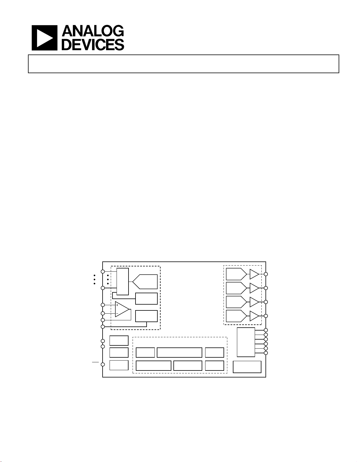
Analog I/O, ARM7TDMI MCU
ADuC7019/20/21/22/24/25/26/27/28/29
On-chip peripherals
UART, 2× I
Up to 40-pin GPIO port
4× general-purpose timers
Wake-up and watchdog timers (WDT)
Power supply monitor
3-phase, 16-bit PWM generator
Programmable logic array (PLA)
External memory interface, up to 512 kB
Power
Specified for 3 V operation
Active mode: 11 mA @ 5 MHz, 40 mA @ 41.78 MHz
Packages and temperature range
From 40-lead 6 mm × 6 mm LFCSP to 80-lead LQFP
Fully specified for –40°C to +125°C operation
Tools
Low cost QuickStart™ development system
Full third-party support
APPLICATIONS
Industrial control and automation systems
Smart sensors, precision instrumentation
Base station systems, optical networking
FUNCTIONAL BLOCK DIAGRAM
2
C® and SPI serial I/O
1
1
1
1
ADC0
1MSPS
12-BIT ADC
TEMP
SENSOR
BAND GAP
REF
ARM7TDMI-BASED M CU WI TH
ADDITIONAL PERIPHERALS
PLA
31k × 16 FLASH/ EEPROM
4 GENERAL-
PURPOSE TI MERS
2k × 32 SRAM
ADC11
CMP0
CMP1
CMP
V
XCLKI
XCLKO
OUT
REF
RST
MUX
OSC
AND PLL
PSM
POR
1
Depending on part model. See Ordering Guide for more information.
Rev. D
Information furnished by Analog Devices is believed to be accurate and reliable. However, no
responsibility is assumed by Anal og Devices for its use, nor for any infringements of patents or ot her
rights of third parties that may result from its use. Specifications subject to change without notice. No
license is granted by implication or otherwise under any patent or patent rights of Analog Devices.
Trademarks and registered trademarks are the property of their respective owners.
ADuC7026
SERIAL I/O
UART, SPI, I
12-BIT
DAC
12-BIT
DAC
12-BIT
DAC
12-BIT
DAC
3-PHASE
PWM
GPIO
JTAG
2
C
EXT. MEMORY
INTERFACE
DAC0
DAC1
DAC2
DAC3
PWM0
PWM0
PWM1
PWM1
PWM2
PWM2
H
L
H
L
H
L
04955-001
Figure 1.
One Technology Way, P.O. Box 9106, Norwood, MA 02062-9106, U.S.A.
Tel: 781.329.4700 www.analog.com
Fax: 781.461.3113 ©2005-2011 Analog Devices, Inc. All rights reserved.
Page 2

ADuC7019/20/21/22/24/25/26/27/28/29
TABLE OF CONTENTS
Features.............................................................................................. 1
Applications....................................................................................... 1
Functional Block Diagram .............................................................. 1
Revision History ............................................................................... 3
General Description ......................................................................... 4
Detailed Block Diagram .............................................................. 5
Specifications..................................................................................... 6
Timing Specifications .................................................................. 9
Absolute Maximum Ratings.......................................................... 16
ESD Caution................................................................................ 16
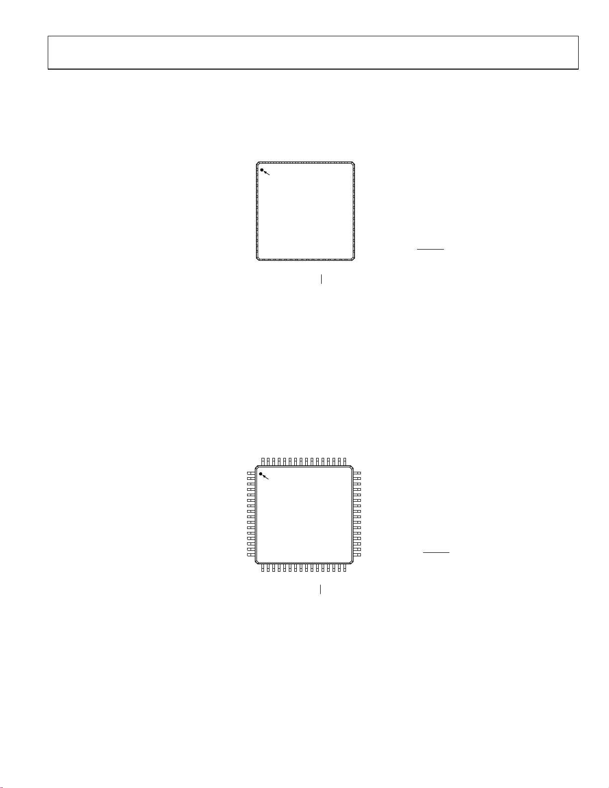
Pin Configurations and Function Descriptions ......................... 17
ADuC7019/ADuC7020/ADuC7021/ADuC7022 .................. 17
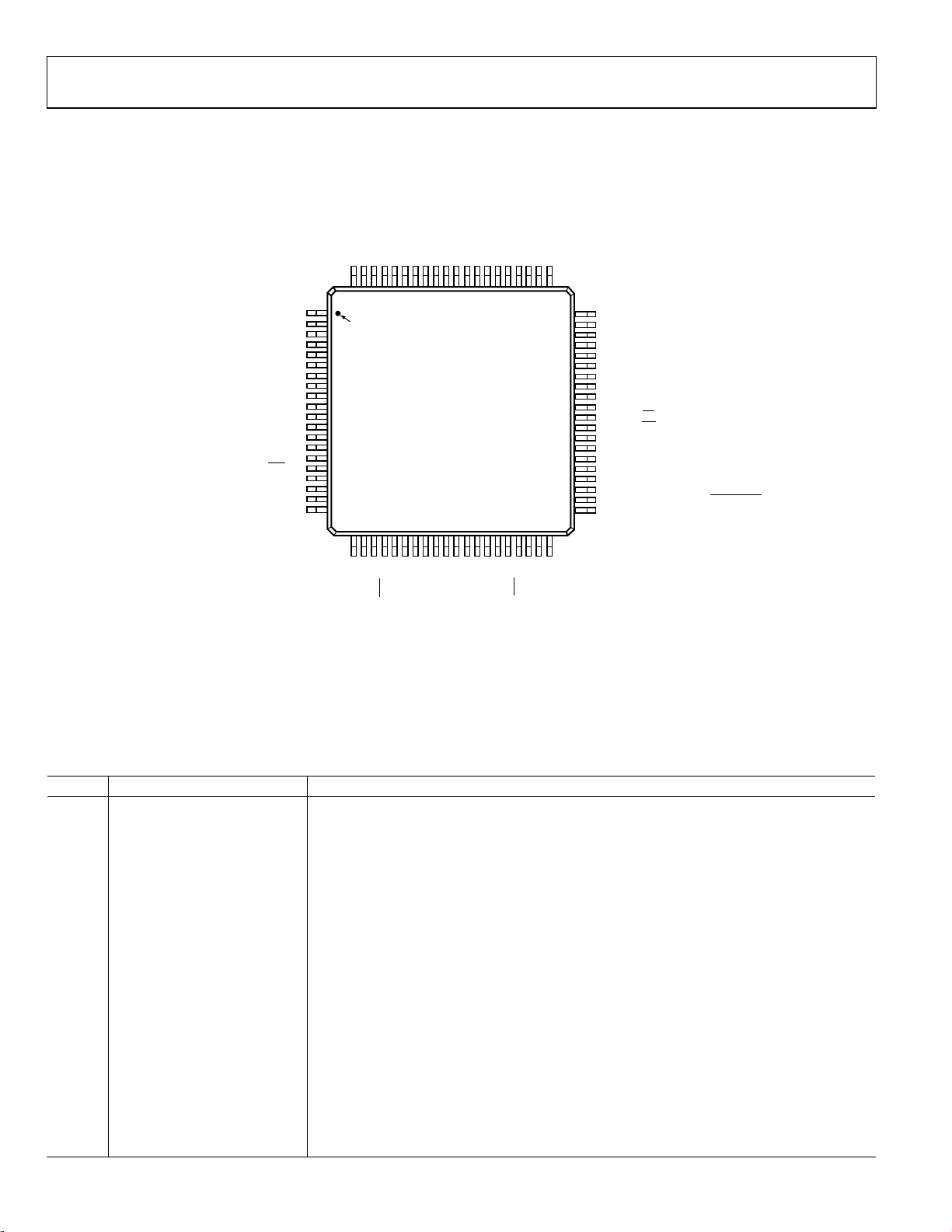
ADuC7024/ADuC7025 .............................................................21
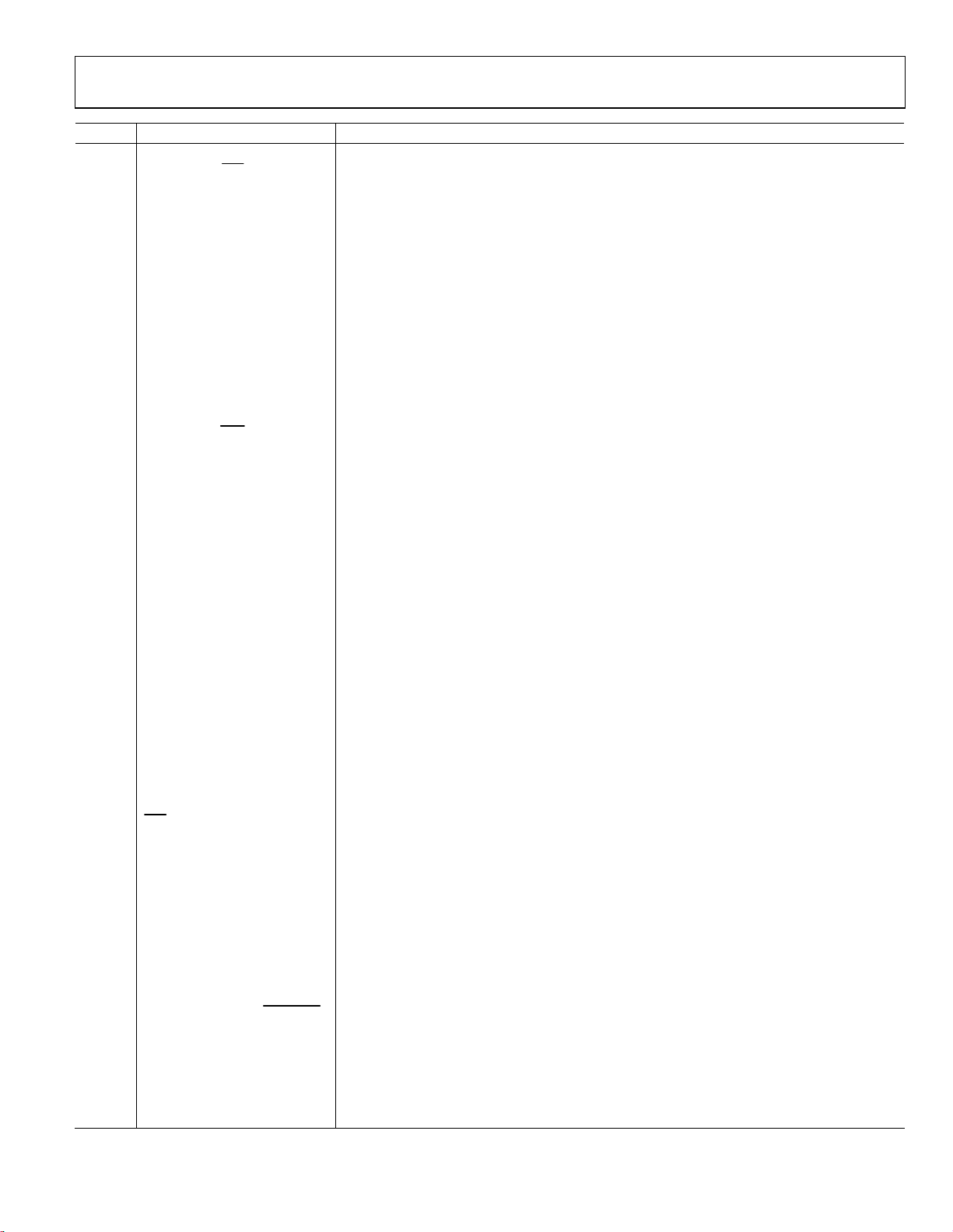
ADuC7026/ADuC7027 .............................................................24
ADuC7028................................................................................... 27
ADuC7029................................................................................... 29
Typical Performance Characteristics ........................................... 31
Terminology .................................................................................... 34
ADC Specifications ....................................................................34
DAC Specifications..................................................................... 34
Overview of the ARM7TDMI Core ............................................. 35
Thumb Mode (T)........................................................................ 35
Long Multiply (M)...................................................................... 35
EmbeddedICE (I) ....................................................................... 35
Exceptions ................................................................................... 35
ARM Registers ............................................................................ 35
Interrupt Latency........................................................................ 36
Memory Organization ...................................................................37
Memory Access........................................................................... 37
Flash/EE Memory....................................................................... 37
SRAM........................................................................................... 37
Memory Mapped Registers....................................................... 37
ADC Circuit Overview .................................................................. 41
Transfer Function....................................................................... 41
Typical Operation....................................................................... 42
MMRs Interface.......................................................................... 42
Converter Operation.................................................................. 44
Driving the Analog Inputs ........................................................ 45
Calibration................................................................................... 46
Temperature Sensor ................................................................... 46
Band Gap Reference................................................................... 46
Nonvolatile Flash/EE Memory ..................................................... 47
Programming.............................................................................. 47
Security ........................................................................................ 48
Flash/EE Control Interface ....................................................... 48
Execution Time from SRAM and Flash/EE............................ 50
Reset and Remap ........................................................................ 50
Other Analog Peripherals.............................................................. 52
DAC.............................................................................................. 52
Power Supply Monitor............................................................... 53
Comparator................................................................................. 53
Oscillator and PLL—Power Control........................................ 54
Digital Peripherals.......................................................................... 57
3-Phase PWM............................................................................. 57
Description of the PWM Block ................................................ 58
General-Purpose Input/Output................................................ 63
Serial Port Mux........................................................................... 65
UART Serial Interface................................................................ 65
Serial Peripheral Interface......................................................... 69
I2C-Compatible Interfaces......................................................... 71
Programmable Logic Array (PLA)........................................... 75
Processor Reference Peripherals................................................... 78
Interrupt System......................................................................... 78
Timers.......................................................................................... 79
External Memory Interfacing................................................... 83
Hardware Design Considerations ................................................ 87
Power Supplies............................................................................ 87
Grounding and Board Layout Recommendations................. 88
Clock Oscillator.......................................................................... 88
Power-On Reset Operation....................................................... 89
Typical System Configuration .................................................. 89
Development Tools......................................................................... 90
PC-Based Tools........................................................................... 90
In-Circuit Serial Downloader................................................... 90
Outline Dimensions....................................................................... 91
Ordering Guide .......................................................................... 95
Rev. D | Page 2 of 96
Page 3

ADuC7019/20/21/22/24/25/26/27/28/29
REVISION HISTORY
5/11—Rev. C to Rev. D
Changes to Table 4 ..........................................................................11
Changes to Table 105......................................................................67
Updated Outline Dimensions........................................................91
Changes to Ordering Guide...........................................................95
12/09—Rev. B to Rev. C
Added ADuC7029 Part .....................................................Universal
Added Table Numbers and Renumbered Tables............... Universal
Changes to Figure Numbers .............................................Universal
Changes to Table 1 ............................................................................6
Changes to Figure 3 ..........................................................................9
Changes to Table 3 and Figure 4 ...................................................10
Changes to Table 10 ........................................................................16
Changes to Figure 55 ......................................................................53
Changes to Serial Peripheral Interface Section ...........................69
Changes to Table 137......................................................................73
Changes to Figure 71 and Figure 72 .............................................85
Changes to Figure 73 and Figure 74 .............................................86
Updated Outline Dimensions........................................................91
Changes to Ordering Guide...........................................................94
3/07—Rev. A to Rev. B
Added ADuC7028 Part .....................................................Universal
Updated Format.................................................................. Universal
Changes to Figure 2...........................................................................5
Changes to Table 1 ............................................................................6
Changes to ADuC7026/ADuC7027 Section ...............................23
Changes to Figure 21 ......................................................................28
Changes to Figure 32 Caption ....................................................... 30
Changes to Table 14........................................................................35
Changes to ADC Circuit Overview Section................................38
Changes to Programming Section................................................44
Changes to Flash/EE Control Interface Section..........................45
Changes to Table 24........................................................................47
Changes to RSTCLR Register Section..........................................48
Changes to Figure 52 ......................................................................49
Changes to Figure 53 ......................................................................50
Changes to Comparator Section ...................................................50
Changes to Oscillator and PLL—Power Control Section..........51
Changes to Digital Peripherals Section........................................54
Changes to Interrupt System Section ...........................................75
Changes to Timers Section ............................................................76
Changes to External Memory Interfacing Section .....................80
Added IOV
Changes to Ordering Guide...........................................................90
1/06—Rev. 0 to Rev. A
Changes to Table 1............................................................................ 6
Added the Flash/EE Memory Reliability Section ....................... 43
Changes to Table 30........................................................................52
Changes to Serial Peripheral Interface .........................................66
Changes to Ordering Guide...........................................................90
10/05—Revision 0: Initial Version
Supply Sensitivity Section..................................... 84
DD
Rev. D | Page 3 of 96
Page 4

ADuC7019/20/21/22/24/25/26/27/28/29
GENERAL DESCRIPTION
The ADuC7019/20/21/22/24/25/26/27/28/29 are fully integrated,
1 MSPS, 12-bit data acquisition systems incorporating high
performance multichannel ADCs, 16-bit/32-bit MCUs, and
Flash®/EE memory on a single chip.
The ADC consists of up to 12 single-ended inputs. An additional
four inputs are available but are multiplexed with the four DAC
output pins. The four DAC outputs are available only on certain
models (ADuC7020, ADuC7026, ADuC7028, and ADuC7029).
However, in many cases where the DAC outputs are not present,
these pins can still be used as additional ADC inputs, giving a
maximum of 16 ADC input channels. The ADC can operate in
single-ended or differential input mode. The ADC input voltage
is 0 V to V
and voltage comparator complete the ADC peripheral set.
Depending on the part model, up to four buffered voltage
output DACs are available on-chip. The DAC output range is
programmable to one of three voltage ranges.
. A low drift band gap reference, temperature sensor,
REF
The devices operate from an on-chip oscillator and a PLL
generating an internal high frequency clock of 41.78 MHz
(UCLK). This clock is routed through a programmable clock
divider from which the MCU core clock operating frequency
is generated. The microcontroller core is an ARM7TDMI®,
16-bit/32-bit RISC machine, which offers up to 41 MIPS peak
performance. Eight kilobytes of SRAM and 62 kilobytes of
nonvolatile Flash/EE memory are provided on-chip. The
ARM7TDMI core views all memory and registers as a single
linear array.
On-chip factory firmware supports in-circuit serial download
via the UART or I
2
C serial interface port; nonintrusive emulation
is also supported via the JTAG interface. These features are
incorporated into a low cost QuickStart™ development system
supporting this MicroConverter® family.
The parts operate from 2.7 V to 3.6 V and are specified over an
industrial temperature range of −40°C to +125°C. When
operating at 41.78 MHz, the power dissipation is typically
120 mW. The ADuC7019/20/21/22/24/25/26/27/28/29 are
available in a variety of memory models and packages (see
Ordering Guide).
Rev. D | Page 4 of 96
Page 5
ADuC7019/20/21/22/24/25/26/27/28/29
DETAILED BLOCK DIAGRAM
DD
DACGND75DACV
70
12-BIT
12-BIT
12-BIT
12-BIT
3-PHASE
PWM
PLL
INTERRUPT
CONTROLLER
17
33
35
36
48
/MS1
/MS2
L
/MS00
H
H
P2.3/AE
/PLAO[7]
L
P2.5/PWM0
P2.6/PWM1
P2.4/PWM0
P2.2/RS/ PWM0
*SEE ORDERI NG GUIDE FO R
FEATURE AVAILAB ILITY ON
DIFFERENT M ODELS.
69
BUF
BUF
BUF
BUF
REF
DAC
10
DAC0*/ADC1 2
11
DAC1*/ADC1 3
12
DAC2*/ADC1 4
13
DAC3*/ADC1 5
29
P3.0/AD0/PWM0H/PLAI[8]
30
P3.1/AD1/PWM0L/PLAI[9]
31
P3.2/AD2/PWM1H/PLAI[10]
32
P3.3/AD3/PWM1L/PLAI[11]
38
P3.4/AD4/PWM2H/PLAI[12]
39
P3.5/AD5/PWM2L/PLAI[13]
46
P3.6/AD6/PWM
47
P3.7/AD7/PWM
OSC
44
XCLKO
45
XCLKI
43
P0.7/ECLK/XCLK/ SPM8/PLAO[4]
40
IRQ0/P0.4/PWM
41
IRQ1/P0.5/ADC
24
16
/BLE
/MS3
/BHE
L
H
L
P2.7/PWM1
P0.1/PWM2
P0.2/PWM2
/PLAI[14]
TRIP
/PLAI[15]
SYNC
/PLAO[1]/MS1
TRIP
/PLAO[2]/MS2
BUSY
04955-002
BM/P0.0/CMP
P4.6/AD14/PLAO[14]
P4.7/AD15/PLAO[15]
ADC2/CMP 0
ADC3/CMP 1
/PLAI[7]/MS0
OUT
ADC0
ADC1
ADC4
ADC5
ADC6
ADC7
ADC8
ADC9
ADC10
ADC11
ADCNEG
V
REF
77
78
79
80
1
2
3
4
5
6
7
76
9
DAC
20
68
18
PROG. LO GIC
19
55
P4.0/AD8/PLAO[8]56P4.1/AD9/PLAO[9]
REF
ARRAY
REFGND71AGND72AGND8GND
67
MUX
MUX
BAND GAP
REFERENCE
63
P4.2/AD10/PLAO[10]64P4.3/AD11/ PLAO[11]65P4.4/AD12/PLAO[12]66P4.5/AD13/ PLAO[13]
DD
DD
AV
AV
74
73
12-BIT SAR
ADC 1MSPS
TEMP
SENSOR
8192 BYTES USER RAM
/IRQ
OUT
SPI/I2C SERIAL
INTERFACE
V
CMP
REF
SERIAL PORT MULTI PLEXER
62
61
P1.1/SPM 1/PLAI[1]60P1.2/SPM 2/PLAI[2]59P1.3/SPM 3/PLAI[3]
P1.0/T1/SPM0/PLAI[0]
DD
IOGND
25
53
ADuC7026*
ADC
CONTROL
62kB FLASH/EE
(31k × 16 BITS)
(2k × 32 BITS)
DOWNLO ADER
UART
SERIAL PORT
58
52
P1.6/SPM 6/PLAI[6]
P1.4/SPM 4/PLAI[4]/I RQ257P1.5/SPM 5/PLAI[5]/I RQ3
IOGND26IOV
51
DD
IOV
54
P1.7/SPM7/PLAO[0]
ARM7TDMI
14
42
TMS
START
P2.0/SPM9/PLAO[5]/CONV
Figure 2.
15
MCU
CORE
JTAG
EMULATO R
23
TDI
DD
RST27LV
DGND
37
28
VOLTAGE
OUTPUT DAC
VOLTAGE
DAC
CONTROL
OUTPUT DAC
VOLTAGE
OUTPUT DAC
VOLTAGE
OUTPUT DAC
WAKE-UP/
RTC TIMER
POWER SUPPLY
MONITOR
PROG. CLOCK
DIVIDER
POR
22
21
49
34
TCK
TDO
BUSY
P0.3/TRST/A16/ADC
50
/PLAO[6]
H
P0.6/T1/MRST/PLAO[3]
P2.1/W S/PWM0
Rev. D | Page 5 of 96
Page 6

ADuC7019/20/21/22/24/25/26/27/28/29
SPECIFICATIONS
AVDD = IOVDD = 2.7 V to 3.6 V, V
Table 1.
Parameter Min Typ Max Unit Test Conditions/Comments
ADC CHANNEL SPECIFICATIONS Eight acquisition clocks and fADC/2
ADC Power-Up Time 5 s
DC Accuracy
1, 2
Resolution 12 Bits
Integral Nonlinearity ±0.6 ±1.5 LSB 2.5 V internal reference
±1.0 LSB 1.0 V external reference
Differential Nonlinearity
3, 4
+0.7/−0.6 LSB 1.0 V external reference
DC Code Distribution 1 LSB ADC input is a dc voltage
ENDPOINT ERRORS
5
Offset Error ±1 ±2 LSB
Offset Error Match ±1 LSB
Gain Error ±2 ±5 LSB
Gain Error Match ±1 LSB
DYNAMIC PERFORMANCE fIN = 10 kHz sine wave, f
Signal-to-Noise Ratio (SNR) 69 dB Includes distortion and noise components
Total Harmonic Distortion (THD) −78 dB
Peak Harmonic or Spurious Noise
(PHSN)
Channel-to-Channel Crosstalk −80 dB Measured on adjacent channels
ANALOG INPUT
Input Voltage Ranges
Differential Mode V
Single-Ended Mode 0 to V
Leakage Current ±1 ±6 µA
Input Capacitance 20 pF During ADC acquisition
ON-CHIP VOLTAGE REFERENCE 0.47 µF from V
Output Voltage 2.5 V
Accuracy ±5 mV TA = 25°C
Reference Temperature Coefficient ±40 ppm/ °C
Power Supply Rejection Ratio 75 dB
Output Impedance 70 Ω TA = 25°C
Internal V
Power-On Time 1 ms
REF
EXTERNAL REFERENCE INPUT
Input Voltage Range 0.625
DAC CHANNEL SPECIFICATIONS RL = 5 kΩ, CL = 100 pF
DC Accuracy7
Resolution 12 Bits
Relative Accuracy ±2 LSB
Differential Nonlinearity ±1 LSB Guaranteed monotonic
Offset Error ±15 mV 2.5 V internal reference
Gain Error8 ±1 %
Gain Error Mismatch 0.1 % % of full scale on DAC0
ANALOG OUTPUTS
Output Voltage Range_0 0 to DAC
Output Voltage Range_1 0 to 2.5 V
Output Voltage Range_2 0 to DACVDD V
Output Impedance 2 Ω
= 2.5 V internal reference, f
REF
= 41.78 MHz, TA = −40°C to +125°C, unless otherwise noted.
CORE
±0.5 +1/−0.9 LSB 2.5 V internal reference
−75 dB
6
± V
CM
AVDD V
V DAC
REF
/2 V
REF
V
REF
to AGND
REF
range: DACGND to DACVDD
REF
SAMPLE
= 1 MSPS
Rev. D | Page 6 of 96
Page 7

ADuC7019/20/21/22/24/25/26/27/28/29
Parameter Min Typ Max Unit Test Conditions/Comments
DAC AC CHARACTERISTICS
Voltage Output Settling Time 10 µs
Digital-to-Analog Glitch Energy ±20 nV-sec
COMPARATOR
Input Offset Voltage ±15 mV
Input Bias Current 1 µA
Input Voltage Range AGND AVDD − 1.2 V
Input Capacitance 7 pF
Hysteresis
4, 6
2 15 mV
Response Time 3 µs
TEMPERATURE SENSOR
Voltage Output at 25°C 780 mV
Voltage TC −1.3 mV/°C
Accuracy ±3 °C
POWER SUPPLY MONITOR (PSM)
IOVDD Trip Point Selection 2.79 V Two selectable trip points
3.07 V
Power Supply Trip Point Accuracy ±2.5 % Of the selected nominal trip point voltage
POWER-ON-RESET 2.36 V
GLITCH IMMUNITY ON RESET PIN3 50 µs
WATCHD OG T IME R ( WDT )
Timeout Period
0 512 sec
FLASH/EE MEMORY
Endurance9 10,000 Cycles
Data Retention10 20 Years TJ = 85°C
DIGITAL INPUTS All digital inputs excluding XCLKI and XCLKO
Logic 1 Input Current ±0.2 ±1 µA VIH = IOVDD or VIH = 5 V
Logic 0 Input Current −40 −60 µA
−80 −120 µA VIL = 0 V; TDI on ADuC7019/20/21/22/24/25/29
Input Capacitance 10 pF
LOGIC INPUTS3 All logic inputs excluding XCLKI
V
, Input Low Voltage 0.8 V
INL
V
, Input High Voltage 2.0 V
INH
LOGIC OUTPUTS All digital outputs excluding XCLKO
VOH, Output High Voltage 2.4 V I
VOL, Output Low Voltage11 0.4 V I
CRYSTAL INPUTS XCLKI and XCLKO
Logic Inputs, XCLKI Only
V
, Input Low Voltage 1.1 V
INL
V
, Input High Voltage 1.7 V
INH
XCLKI Input Capacitance 20 pF
XCLKO Output Capacitance 20 pF
INTERNAL OSCILLATOR 32.768 kHz
±3 %
±24 % TA = 0°C to 85°C range
1 LSB change at major carry (where maximum
number of bits simultaneously changes in the
DACxDAT register)
Hysteresis turned on or off via the CMPHYST bit
in the CMPCON register
100 mV overdrive and configured with CMPRES =
11
= 0 V; except TDI on
V
IL
ADuC7019/20/21/22/24/25/29
= 1.6 mA
SOURCE
= 1.6 mA
SINK
Rev. D | Page 7 of 96
Page 8

ADuC7019/20/21/22/24/25/26/27/28/29
Parameter Min Typ Max Unit Test Conditions/Comments
MCU CLOCK RATE
From 32 kHz Internal Oscillator 326 kHz CD12 = 7
From 32 kHz External Crystal 41.78 MHz CD12 = 0
Using an External Clock 0.05 44 MHz TA = 85°C
0.05 41.78 MHz TA = 125°C
START-UP TIME Core clock = 41.78 MHz
At Power-On 130 ms
From Pause/Nap Mode 24 ns CD12 = 0
3.06 µs CD12 = 7
From Sleep Mode 1.58 ms
From Stop Mode 1.7 ms
PROGRAMMABLE LOGIC ARRAY (PLA)
Pin Propagation Delay 12 ns From input pin to output pin
Element Propagation Delay 2.5 ns
POWER REQUIREMENTS
Power Supply Voltage Range
AVDD to AGND and IOVDD to IOGND 2.7 3.6 V
Analog Power Supply Currents
AVDD Current 200 µA ADC in idle mode; all parts except ADuC7019
400 µA ADC in idle mode; ADuC7019 only
DACVDD Current15 3 25 µA
Digital Power Supply Current
IOVDD Current in Normal Mode Code executing from Flash/EE
7 10 mA CD12 = 7
11 15 mA CD12 = 3
40 45 mA CD12 = 0 (41.78 MHz clock)
IOVDD Current in Pause Mode 25 30 mA CD12 = 0 (41.78 MHz clock)
IOVDD Current in Sleep Mode 250 400 µA TA = 85°C
600 1000 µA TA = 125°C
Additional Power Supply Currents
ADC 2 mA @ 1 MSPS
0.7 mA @ 62.5 kSPS
DAC 700 µA per DAC
ESD TESTS 2.5 V reference, TA = 25°C
HBM Passed Up To 4 kV
FCIDM Passed Up To 0.5 kV
1
All ADC channel specifications are guaranteed during normal MicroConverter core operation.
2
Apply to all ADC input channels.
3
Measured using the factory-set default values in the ADC offset register (ADCOF) and gain coefficient register (ADCGN).
4
Not production tested but supported by design and/or characterization data on production release.
5
Measured using the factory-set default values in ADCOF and ADCGN with an external AD845 op amp as an input buffer stage as shown in Figure 49. Based on external ADC
system components; the user may need to execute a system calibration to remove external endpoint errors and achieve these specifications (see the Calibration section).
6
The input signal can be centered on any dc common-mode voltage (VCM) as long as this value is within the ADC voltage input range specified.
7
DAC linearity is calculated using a reduced code range of 100 to 3995.
8
DAC gain error is calculated using a reduced code range of 100 to internal 2.5 V V
9
Endurance is qualified as per JEDEC Standard 22, Method A117 and measured at −40°C, +25°C, +85°C, and +125°C.
10
Retention lifetime equivalent at junction temperature (TJ) = 85°C as per JEDEC Standard 22m, Method A117. Retention lifetime derates with junction temperature.
11
Test carried out with a maximum of eight I/Os set to a low output level.
12
See the POWCON register.
13
Power supply current consumption is measured in normal, pause, and sleep modes under the following conditions: normal mode with 3.6 V supply, pause mode with
3.6 V supply, and sleep mode with 3.6 V supply.
14
IOVDD power supply current decreases typically by 2 mA during a Flash/EE erase cycle.
15
On the ADuC7019/20/21/22, this current must be added to the AVDD current.
13, 14
.
REF
Rev. D | Page 8 of 96
Page 9
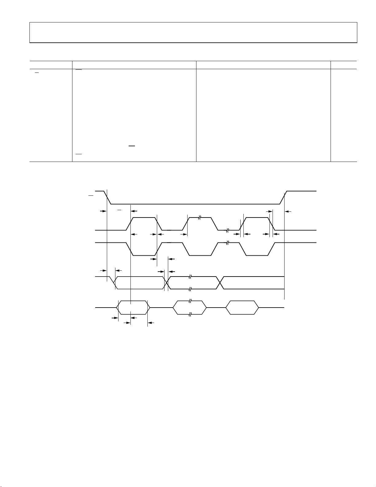
ADuC7019/20/21/22/24/25/26/27/28/29
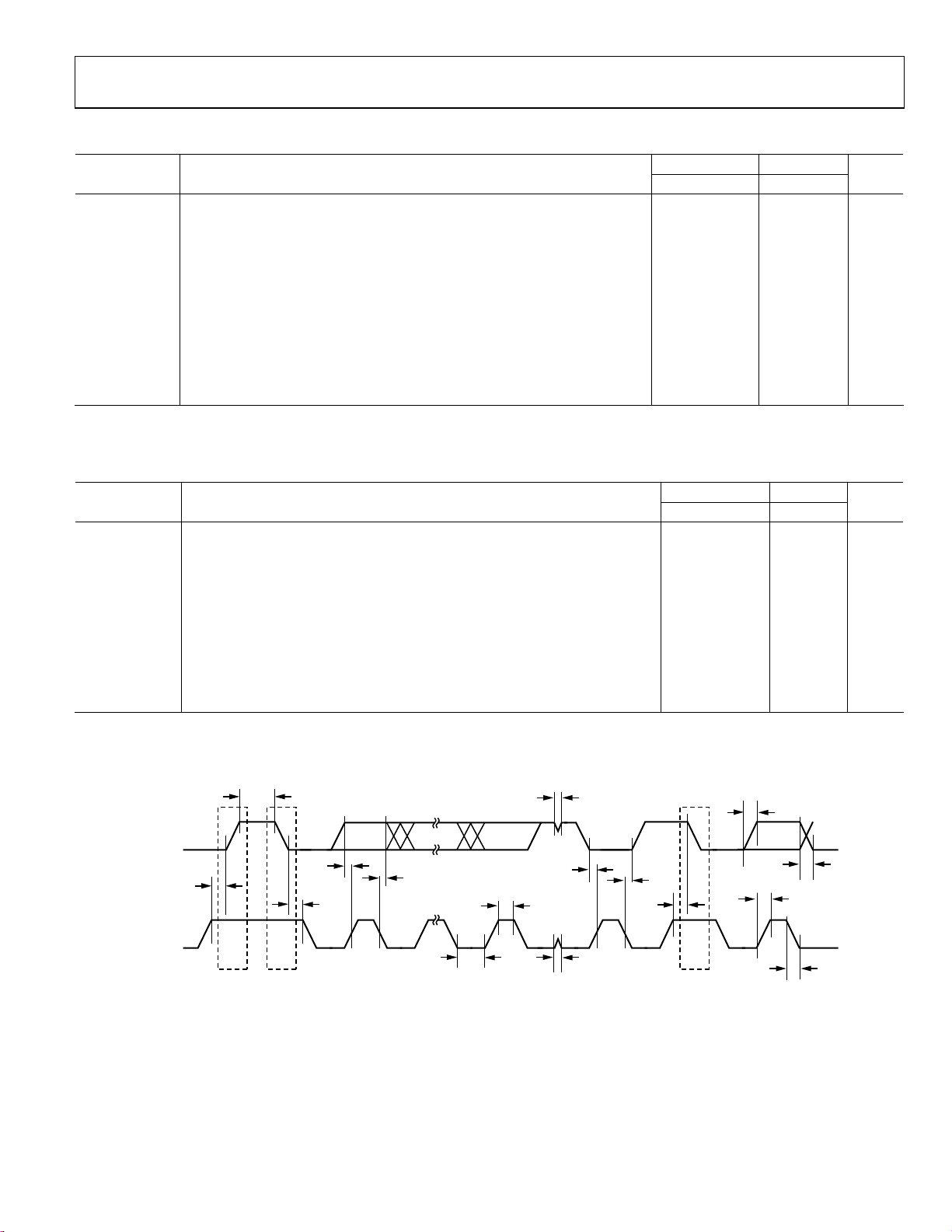
TIMING SPECIFICATIONS
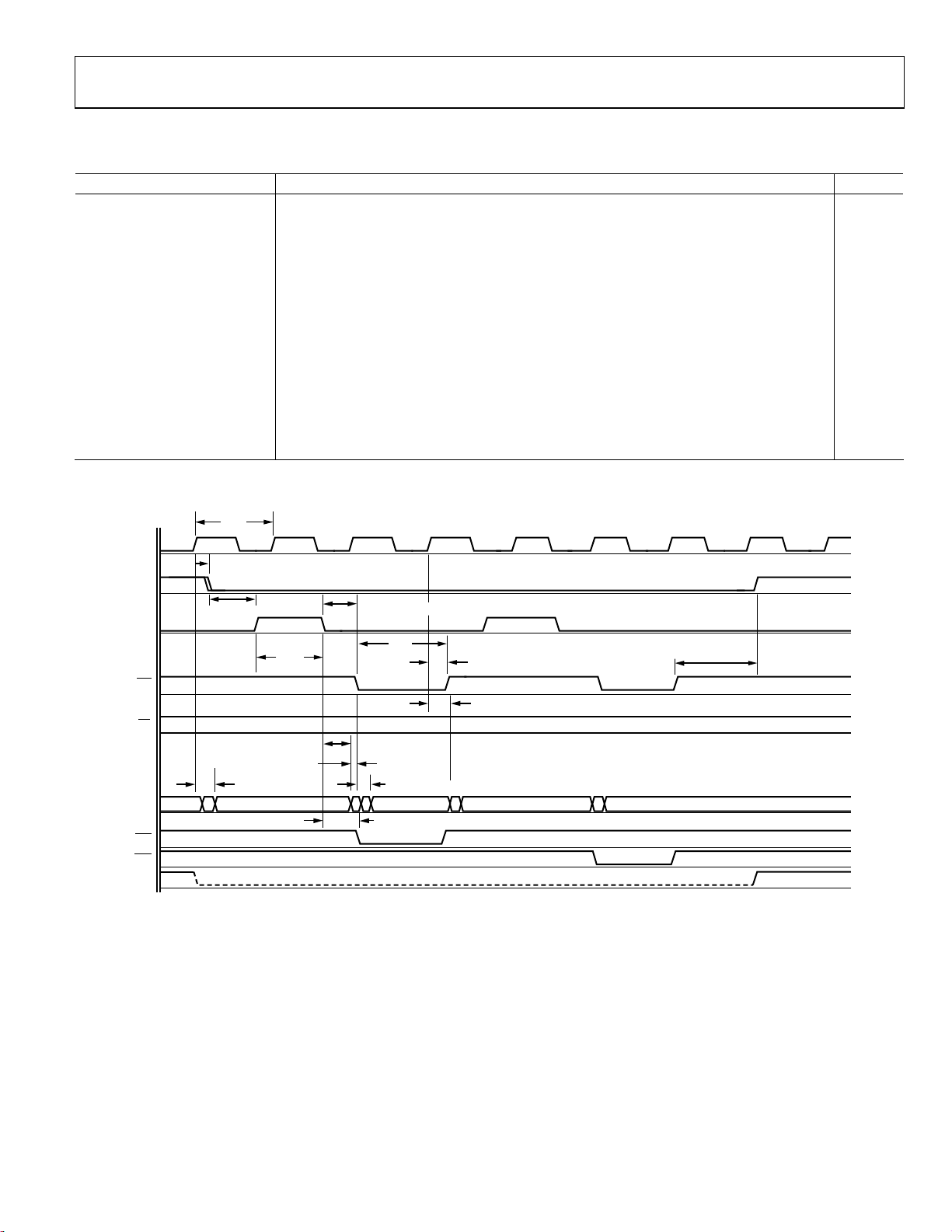
Table 2. External Memory Write Cycle
Parameter Min Typ Max Unit
CLK1 UCLK
t
MS_AFTER_CLKH
t
ADDR_AFTER_CLKH
t
AE_H_AFTER_MS
tAE (XMxPAR[14:12] + 1) × CLK
t
HOLD_ADDR_AFTER_AE_L
t
HOLD_ADDR_BEFORE_WR_L
t
WR_L_AFTER_AE_L
t
DATA_AFTER_WR_L
tWR (XMxPAR[7:4] + 1) × CLK
t
WR_H_AFTER_CLKH
t
HOLD_DATA_AFTER_WR_H
t
BEN_AFTER_AE_L
t
RELEASE_MS_AFTER_WR_H
1
See Table 78.
0 4 ns
4 8 ns
½ CLK
½ CLK + (!XMxPAR[10]) × CLK
(!XMxPAR[8]) × CLK
½ CLK + (!XMxPAR[10] + !XMxPAR[8]) × CLK
8 12 ns
0 4 ns
(!XMxPAR[8]) × CLK
½ CLK
(!XMxPAR[8] + 1) × CLK
CLK
CLK
t
MS_AFTER_ CLKH
MSx
t
t
AE
WS
RS
AD[16:1] FFFF 9ABC 5678 9ABE 1234
BLE
BHE
A16
AE_H_AFTER_M S
t
AE
t
HOLD_ADDR_A FTER_AE_L
t
HOLD_ADDR_B EFORE_WR_L
t
ADDR_AFTER_CLKH
WR_L_AFTER_AE_L
t
WR
t
WR_H_AFTER_ CLKH
t
HOLD_DATA_A FTER_WR_H
t
DATA_AFTER_WR_L
t
BEN_AFTER_AE_L
Figure 3. External Memory Write Cycle (See Table 78)
t
RELEASE_MS_AFTER_WR_H
04955-052
Rev. D | Page 9 of 96
Page 10
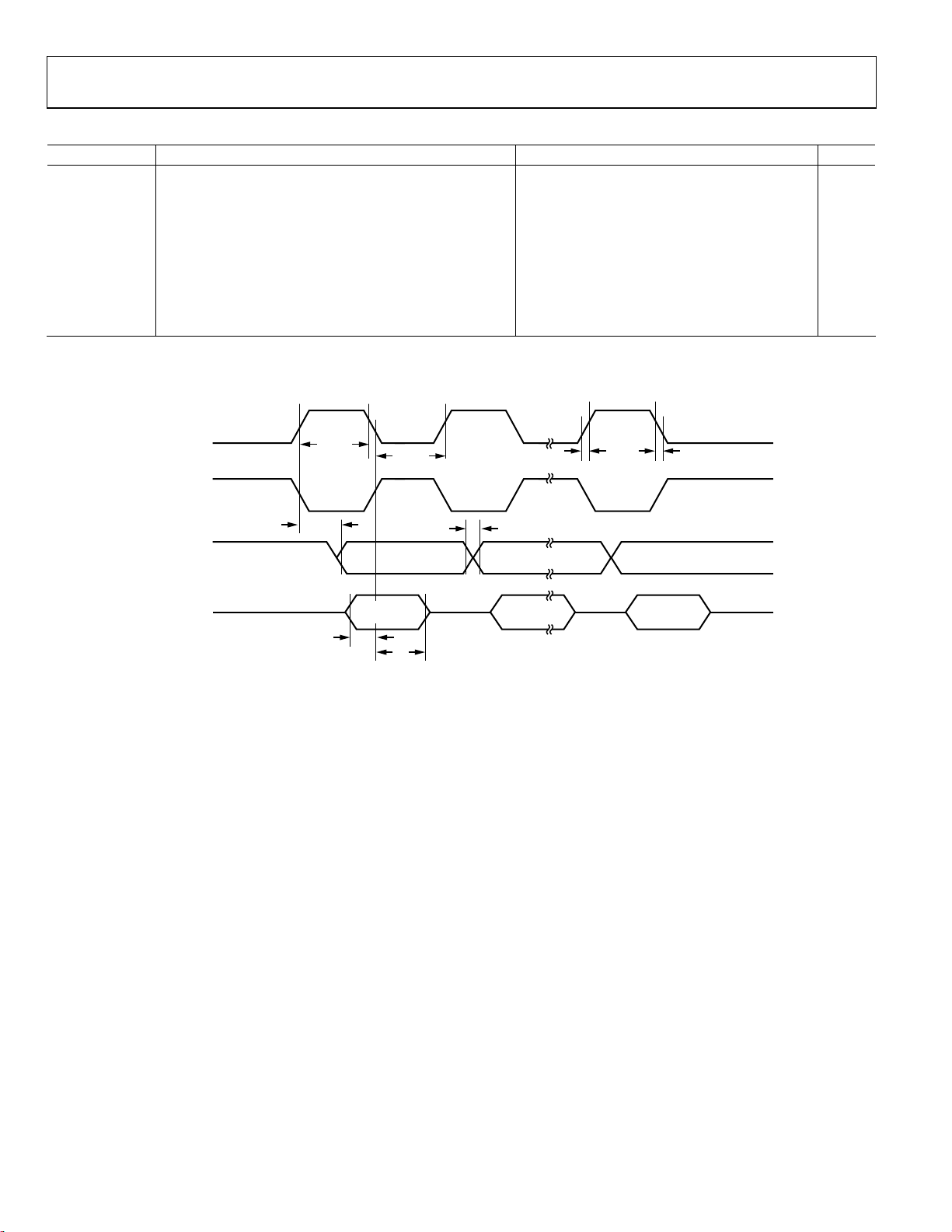
ADuC7019/20/21/22/24/25/26/27/28/29
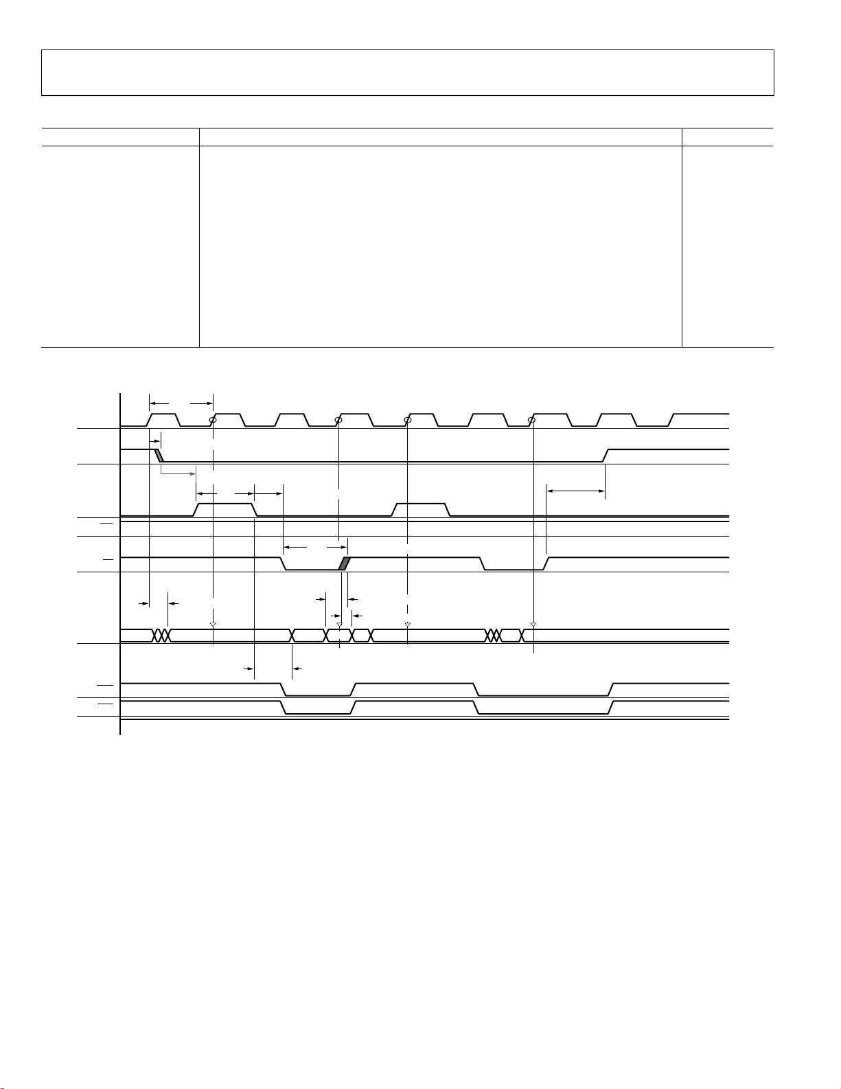
Table 3. External Memory Read Cycle
Parameter Min Typ Max Unit
CLK1 1/MD clock ns typ × (POWCON[2:0] + 1)
t
MS_AFTER_CLKH
t
ADDR_AFTER_CLKH
t
AE_H_AFTER_MS
tAE (XMxPAR[14:12] + 1) × CLK
t
HOLD_ADDR_AFTER_AE_L
t
RD_L_AFTER_AE_L
t
RD_H_AFTER_CLKH
tRD (XMxPAR[3:0] + 1) × CLK
t
DATA_BEFORE_RD_H
t
DATA_AFTER_RD_H
t
RELEASE_MS_AFTER_RD_H
1
See Table 78.
4 8 ns
4 16 ns
½ CLK
½ CLK + (! XMxPAR[10] ) × CLK
½ CLK + (! XMxPAR[10]+ ! XMxPAR[9] ) × CLK
0 4
16 ns
8 + (! XMxPAR[9]) × CLK
1 × CLK
CLK
ECLK
t
MSx
AE
WS
RS
MS_AFTER_CL KH
t
AE_H_AFTER_MS
t
AE
t
RD_L_AFTER_AE _L
t
RD
t
RD_H_AFTER_CLK H
t
RELEASE_MS _AFTER_RD_H
AD[16:1]
BHE
BLE
A16
t
t
ADDR_AFTER_CLKH
FFFF 2348 XXXX CDEF XX 234A XX 89AB
t
HOLD_ADDR_A FTER_AE_L
DATA_BEFOR E_RD_H
t
DATA_AFTER_RD_H
Figure 4. External Memory Read Cycle (See Table 78)
04955-053
Rev. D | Page 10 of 96
Page 11
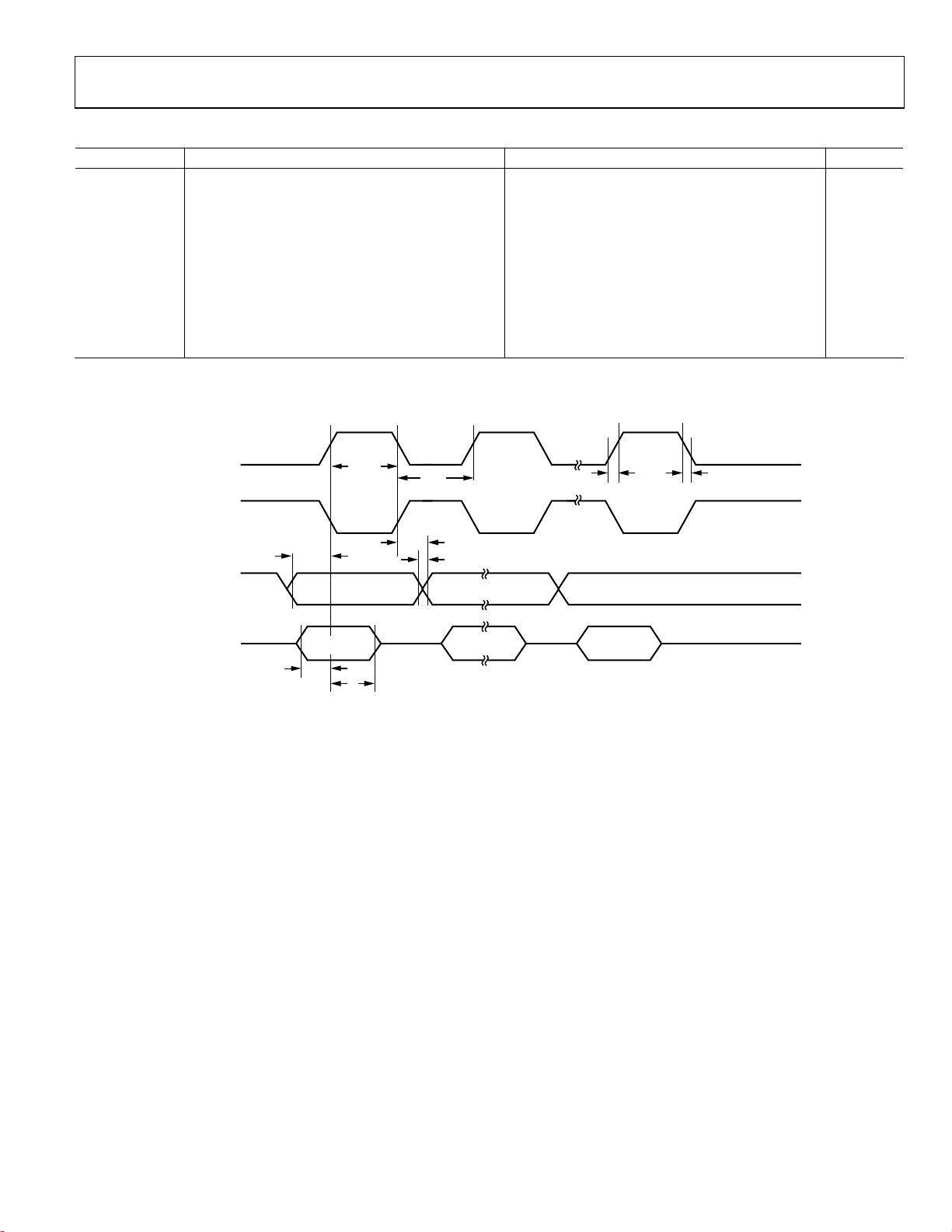
ADuC7019/20/21/22/24/25/26/27/28/29
S
Table 4. I2C Timing in Fast Mode (400 kHz)
Slave Master
Parameter Description Min Max Typ Unit
tL SCLOCK low pulse width1 200 1360 ns
tH SCLOCK high pulse width1 100 1140 ns
t
Start condition hold time 300 ns
SHD
t
Data setup time 100 740 ns
DSU
t
Data hold time 0 400 ns
DHD
t
Setup time for repeated start 100 ns
RSU
t
Stop condition setup time 100 400 ns
PSU
t
Bus-free time between a stop condition and a start condition 1.3
BUF
tR Rise time for both CLOCK and SDATA 300 200 ns
tF Fall time for both CLOCK and SDATA 300 ns
t
Pulse width of spike suppressed 50 ns
SUP
1
t
depends on the clock divider or CD bits in the PLLCON MMR. t
HCLK
HCLK
= t
/2CD; see Figure 57.
UCLK
Table 5. I
2
C Timing in Standard Mode (100 kHz)
Slave Master
Parameter Description Min Max Typ Unit
tL SCLOCK low pulse width1 4.7 µs
tH SCLOCK high pulse width1 4.0 ns
t
Start condition hold time 4.0 µs
SHD
t
Data setup time 250 ns
DSU
t
Data hold time 0 3.45 µs
DHD
t
Setup time for repeated start 4.7 µs
RSU
t
Stop condition setup time 4.0 µs
PSU
t
Bus-free time between a stop condition and a start condition 4.7 µs
BUF
tR Rise time for both CLOCK and SDATA 1 µs
tF Fall time for both CLOCK and SDATA 300 ns
1
t
depends on the clock divider or CD bits in the PLLCON MMR. t
HCLK
HCLK
= t
/2CD; see Figure 57.
UCLK
DATA (I/O)
SCLK (I)
t
PSU
t
BUF
PS
STOP
CONDITIO N
CONDITION
START
MSB LSB ACK MSB
t
DSU
t
SHD
t
DHD
Figure 5. I
2
C Compatible Interface Timing
t
SUP
t
DSU
t
H
t
L
t
SUP
t
RSU
t
DHD
REPEATED
S(R)
START
t
R
t
F
t
R
1982–71
t
F
μs
4955-054
Rev. D | Page 11 of 96
Page 12
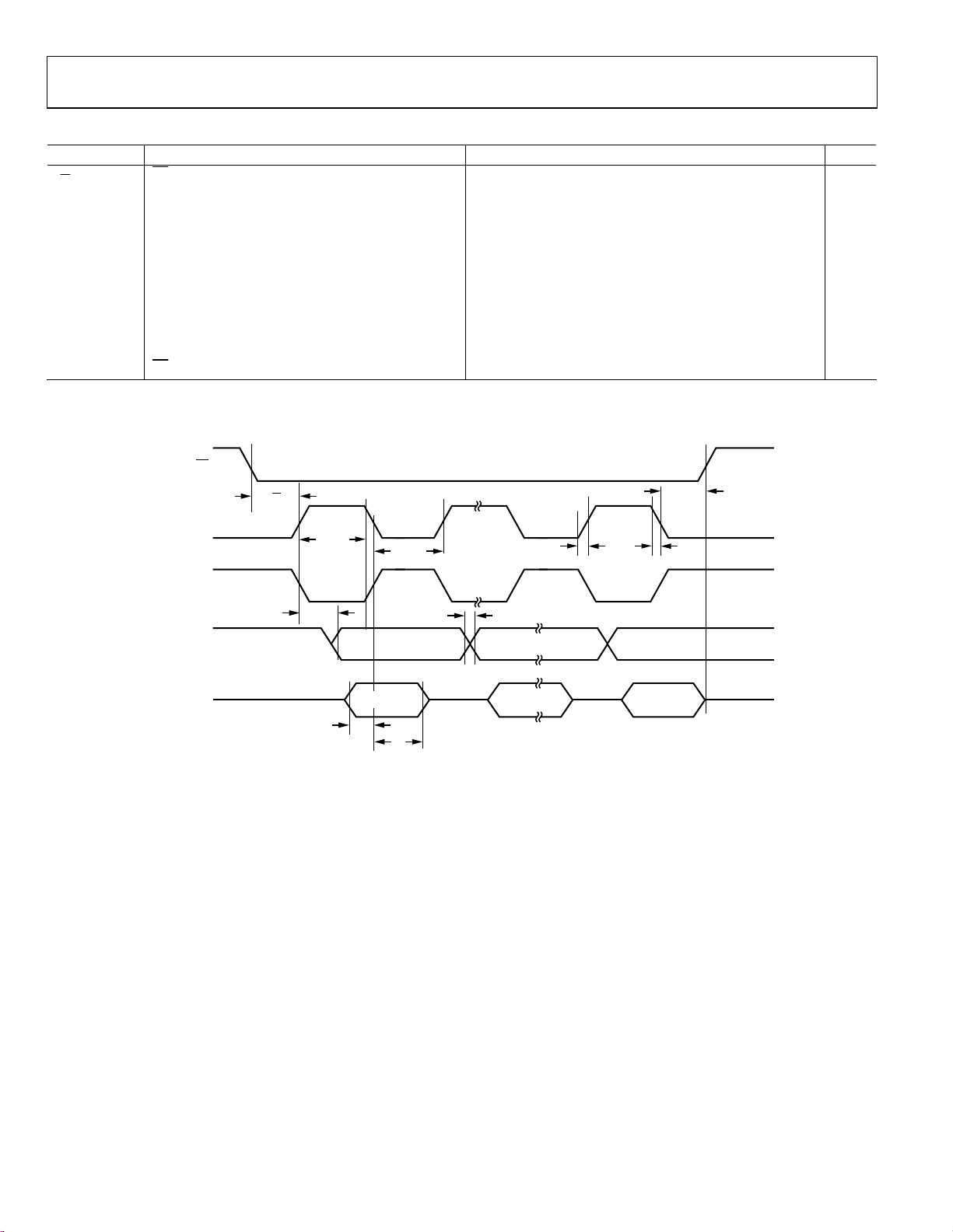
ADuC7019/20/21/22/24/25/26/27/28/29
Table 6. SPI Master Mode Timing (Phase Mode = 1)
Parameter Description Min Typ Max Unit
tSL SCLOCK low pulse width1 (SPIDIV + 1) × t
tSH SCLOCK high pulse width1 (SPIDIV + 1) × t
t
Data output valid after SCLOCK edge 25 ns
DAV
t
Data input setup time before SCLOCK edge2 1 × t
DSU
t
Data input hold time after SCLOCK edge2 2 × t
DHD
ns
UCLK
ns
UCLK
tDF Data output fall time 5 12.5 ns
tDR Data output rise time 5 12.5 ns
tSR SCLOCK rise time 5 12.5 ns
tSF SCLOCK fall time 5 12.5 ns
1
t
depends on the clock divider or CD bits in the PLLCON MMR. t
HCLK
2
t
= 23.9 ns. It corresponds to the 41.78 MHz internal clock from the PLL before the clock divider; see Figure 57.
UCLK
HCLK
= t
UCLK
/2CD; see Figure 57.
ns
HCLK
ns
HCLK
SCLOCK
(POLARITY = 0)
SCLOCK
(POLARITY = 1)
MOSI MSB BITS 6 TO 1 LSB
MISO MSB IN BITS 6 TO 1 LSB IN
t
DAV
t
SH
t
DSU
t
DHD
t
SL
t
DF
t
DR
t
SR
t
SF
4955-055
Figure 6. SPI Master Mode Timing (Phase Mode = 1)
Rev. D | Page 12 of 96
Page 13
ADuC7019/20/21/22/24/25/26/27/28/29
Table 7. SPI Master Mode Timing (Phase Mode = 0)
Parameter Description Min Typ Max Unit
tSL SCLOCK low pulse width1 (SPIDIV + 1) × t
tSH SCLOCK high pulse width1 (SPIDIV + 1) × t
t
Data output valid after SCLOCK edge 25 ns
DAV
t
Data output setup before SCLOCK edge 75 ns
DOSU
t
Data input setup time before SCLOCK edge2 1 × t
DSU
t
Data input hold time after SCLOCK edge2 2 × t
DHD
ns
UCLK
ns
UCLK
tDF Data output fall time 5 12.5 ns
tDR Data output rise time 5 12.5 ns
tSR SCLOCK rise time 5 12.5 ns
tSF SCLOCK fall time 5 12.5 ns
1
t
depends on the clock divider or CD bits in the PLLCON MMR. t
HCLK
2
t
= 23.9 ns. It corresponds to the 41.78 MHz internal clock from the PLL before the clock divider; see Figure 57.
UCLK
HCLK
= t
/2CD; see Figure 57.
UCLK
SCLOCK
(POLARITY = 0)
SCLOCK
(POLARITY = 1)
t
DOSU
MOSI MSB BITS 6 T O 1 LSB
t
SH
t
SL
t
DAV
t
DF
t
DR
t
SR
ns
HCLK
ns
HCLK
t
SF
MISO MSB IN BITS 6 TO 1 LSB IN
t
DSU
t
DHD
Figure 7. SPI Master Mode Timing (Phase Mode = 0)
04955-056
Rev. D | Page 13 of 96
Page 14
ADuC7019/20/21/22/24/25/26/27/28/29
Table 8. SPI Slave Mode Timing (Phsae Mode = 1)
Parameter Description Min Typ Max Unit
tCS
to SCLOCK edge
CS
tSL SCLOCK low pulse width2 (SPIDIV + 1) × t
tSH SCLOCK high pulse width2 (SPIDIV + 1) × t
t
Data output valid after SCLOCK edge 25 ns
DAV
t
Data input setup time before SCLOCK edge1 1 × t
DSU
t
Data input hold time after SCLOCK edge1 2 × t
DHD
tDF Data output fall time 5 12.5 ns
tDR Data output rise time 5 12.5 ns
tSR SCLOCK rise time 5 12.5 ns
tSF SCLOCK fall time 5 12.5 ns
t
SFS
1
t
= 23.9 ns. It corresponds to the 41.78 MHz internal clock from the PLL before the clock divider; see Figure 57.
UCLK
2
t
depends on the clock divider or CD bits in the PLLCON MMR. t
HCLK
high after SCLOCK edge
CS
CS
SCLOCK
(POLARITY = 0)
SCLOCK
(POLARITY = 1)
MISO MSB BITS 6 TO 1 LSB
1
(2 × t
) + (2 × t
HCLK
ns
UCLK
ns
UCLK
) ns
UCLK
ns
HCLK
ns
HCLK
0 ns
= t
/2CD; see Figure 57.
HCLK
UCLK
t
t
CS
t
t
SH
DAV
t
SL
t
DF
t
DR
t
SR
SFS
t
SF
MOSI MSB I N BITS 6 TO 1 LSB IN
t
DSU
t
DHD
Figure 8. SPI Slave Mode Timing (Phase Mode = 1)
04955-057
Rev. D | Page 14 of 96
Page 15
ADuC7019/20/21/22/24/25/26/27/28/29
Table 9. SPI Slave Mode Timing (Phase Mode = 0)
Parameter Description Min Typ Max Unit
tCS
to SCLOCK edge
CS
tSL SCLOCK low pulse width2 (SPIDIV + 1) × t
tSH SCLOCK high pulse width2 (SPIDIV + 1) × t
t
Data output valid after SCLOCK edge 25 ns
DAV
t
Data input setup time before SCLOCK edge1 1 × t
DSU
t
Data input hold time after SCLOCK edge1 2 × t
DHD
tDF Data output fall time 5 12.5 ns
tDR Data output rise time 5 12.5 ns
tSR SCLOCK rise time 5 12.5 ns
tSF SCLOCK fall time 5 12.5 ns
t
DOCS
t
SFS
1
t
= 23.9 ns. It corresponds to the 41.78 MHz internal clock from the PLL before the clock divider; see Figure 57.
UCLK
2
t
depends on the clock divider or CD bits in the PLLCON MMR. t
HCLK
Data output valid after CS
high after SCLOCK edge
CS
CS
SCLOCK
(POLARITY = 0)
SCLOCK
(POLARITY = 1)
MISO
t
DOCS
1
edge
(2 × t
) + (2 × t
HCLK
ns
UCLK
ns
UCLK
) ns
UCLK
ns
HCLK
ns
HCLK
25 ns
0 ns
= t
HCLK
t
CS
t
SH
t
DAV
t
DF
MSB BITS 6 TO 1 LSB
/2CD; see Figure 57.
UCLK
t
SL
t
DR
t
SFS
t
SR
t
SF
MOSI
MSB IN BITS 6 TO 1 LSB IN
t
DSU
t
DHD
Figure 9. SPI Slave Mode Timing (Phase Mode = 0)
Rev. D | Page 15 of 96
04955-058
Page 16
ADuC7019/20/21/22/24/25/26/27/28/29
ABSOLUTE MAXIMUM RATINGS
AGND = REFGND = DACGND = GND
otherwise noted.
Table 10.
Parameter Rating
AVDD to IOVDD −0.3 V to +0.3 V
AGND to DGND −0.3 V to +0.3 V
IOVDD to IOGND, AVDD to AGND −0.3 V to +6 V
Digital Input Voltage to IOGND −0.3 V to +5.3 V
Digital Output Voltage to IOGND −0.3 V to IOVDD + 0.3 V
V
to AGND −0.3 V to AVDD + 0.3 V
REF
Analog Inputs to AGND −0.3 V to AV
Analog Outputs to AGND −0.3 V to AVDD + 0.3 V
Operating Temperature Range, Industrial –40°C to +125°C
Storage Temperature Range –65°C to +150°C
Junction Temperature 150°C
θJA Thermal Impedance
40-Lead LFCSP 26°C/W
49-Ball CSP_BGA 80°C/W
64-Lead LFCSP 24°C/W
64-Ball CSP_BGA 75°C/W
64-Lead LQFP 47°C/W
80-Lead LQFP 38°C/W
Peak Solder Reflow Temperature
SnPb Assemblies (10 sec to 30 sec) 240°C
RoHS Compliant Assemblies
(20 sec to 40 sec)
, TA = 25°C, unless
REF
DD
260°C
+ 0.3 V
Stresses above those listed under Absolute Maximum Ratings
may cause permanent damage to the device. This is a stress
rating only; functional operation of the device at these or any
other conditions above those indicated in the operational
section of this specification is not implied. Exposure to absolute
maximum rating conditions for extended periods may affect
device reliability.
Only one absolute maximum rating can be applied at any one time.
ESD CAUTION
Rev. D | Page 16 of 96
Page 17
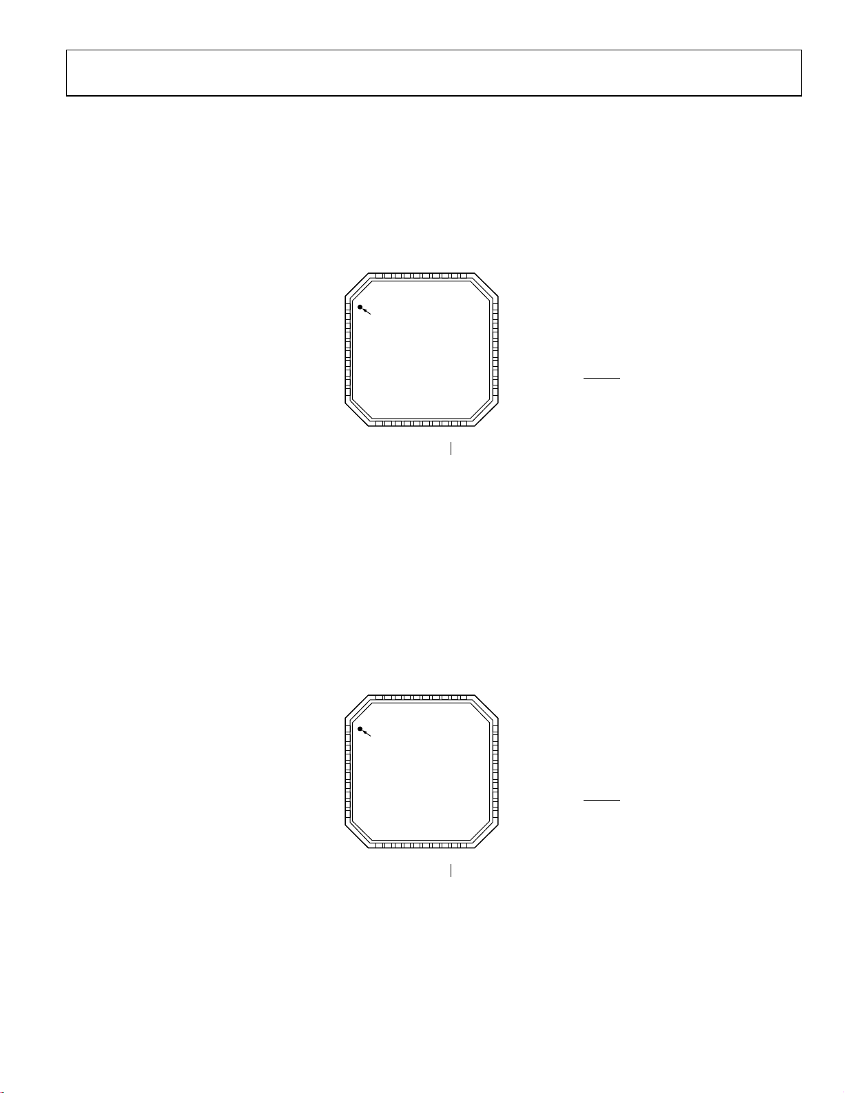
ADuC7019/20/21/22/24/25/26/27/28/29
PIN CONFIGURATIONS AND FUNCTION DESCRIPTIONS
ADuC7019/ADuC7020/ADuC7021/ADuC7022
DD
REF
AGND
V
P4.2/PLAO[10]
P1.0/T1/ SPM0/PLAI[0]
P1.1/SPM 1/PLAI[1]
P1.2/SPM 2/PLAI[2]
31
P1.3/SPM 3/PLAI[3]
30
P1.4/SPM 4/PLAI[4]/I RQ2
29
P1.5/SPM 5/PLAI[5]/I RQ3
28
P1.6/SPM 6/PLAI[6]
27
P1.7/SPM 7/PLAO[0]
26
XCLKI
25
XCLKO
24
P0.7/ECLK/ XCLK/SPM8/PLAO[4]
23
P2.0/SPM 9/PLAO[5]/CONV
22
IRQ1/P0.5/ADC
21
BUSY
/PLAO[2]
START
BM/P0.0/CMP
ADC3/CM P1
ADC4
GND
DAC0/ADC12
DAC1/ADC13
DAC2/ADC14
DAC3/ADC15
TMS
/PLAI[7]
OUT
REF
TDI
ADC2/CMP 0
ADC1
ADC0
AV
403938373635343332
1
PIN 1
2
INDICATO R
3
4
5
6
7
8
9
10
ADuC7019/
ADuC7020
TOP VIEW
(Not to Scale)
111213141516171819
DDLVDD
TCK
TDO
IOV
IOGND
P0.6/T1/MRST/PLAO[3]
NOTES
1. THE EXPOSED PADDLE M UST BE LEFT UNCONNECTED.
20
RST
BUSY
DGND
/PLAO[1]
TRIP
P0.3/TRST/ADC
IRQ0/P0.4/PWM
04955-064
Figure 10. 40-Lead LFCSP_VQ Pin Configuration (ADuC7019/ADuC7020)
DD
REF
AGND
V
P1.0/T1/ SPM0/PLAI[0]
P1.1/SPM 1/PLAI[1]
P1.2/SPM 2/PLAI[2]
31
P1.3/SPM3/PLAI[3]
30
P1.4/SPM4/PLAI[4]/IRQ2
29
P1.5/SPM5/PLAI[5]/IRQ3
28
P1.6/SPM6/PLAI[6]
27
P1.7/SPM7/PLAO[0]
26
XCLKI
25
XCLKO
24
P0.7/ECLK/ XCLK/SPM8/PLAO[ 4]
23
P2.0/SPM9/PLAO[5]/CONV
22
IRQ1/P0.5/ADC
21
BUSY
/PLAO[2]
START
BM/P0.0/CMP
ADC4
ADC5
ADC6
ADC7
GND
DAC0/ADC12
DAC1/ADC13
TMS
/PLAI[7]
OUT
REF
TDI
ADC3/CMP 1
ADC2/CMP 0
ADC1
ADC0
AV
403938373635343332
1
PIN 1
2
INDICATO R
3
4
5
6
7
8
9
10
ADuC7021
TOP VIEW
(Not to Scale)
111213141516171819
DDLVDD
TCK
TDO
IOV
IOGND
P0.6/T1/MRST/PLAO[3]
NOTES
1. THE EXPOSED PADDLE MUST BE LEFT UNCONNECTED.
20
RST
BUSY
DGND
/PLAO[1]
TRIP
P0.3/TRST/ADC
IRQ0/P0.4/PWM
04955-065
Figure 11. 40-Lead LFCSP_VQ Pin Configuration (ADuC7021)
Rev. D | Page 17 of 96
Page 18
ADuC7019/20/21/22/24/25/26/27/28/29
ADC4
ADC3/CMP1
ADC2/CMP0
403938373635343332
DD
REF
AGND
V
P1.0/T1/ SPM0/PLAI[0]
ADC1
ADC0
P1.1/SPM 1/PLAI[1]
AV
31
1
ADC5
ADC6
ADC7
ADC8
ADC9
GND
REF
TMS
TDI
BM/P0.0/CMP
P0.6/T1/MRST/PLAO[3]
NOTES
1. THE EXPOSED PADDLE MUST BE LEFT UNCONNECTED.
OUT
/PLAI[7]
PIN 1
2
INDICAT OR
3
4
5
6
7
8
9
10
ADuC7022
TOP VIEW
(Not to Scale)
111213141516171819
DDLVDD
TCK
TDO
IOV
DGND
IOGND
BUSY
P0.3/ TRST/ADC
RST
/PLAO[1]
TRIP
IRQ0/P0.4/PWM
20
/PLAO[2]
BUSY
IRQ1/P0.5/ADC
30
P1.2/SPM2/PLAI[2]
29
P1.3/SPM3/PLAI[3]
28
P1.4/SPM4/PLAI[4]/IRQ2
27
P1.5/SPM5/PLAI[5]/IRQ3
26
P1.6/SPM6/PLAI[6]
25
P1.7/SPM7/PLAO[0]
24
XCLKI
23
XCLKO
22
P0.7/ECLK/XCLK/SPM8/PLAO[4]
21
P2.0/ SPM9/PLAO[ 5]/CONV
START
04955-066
Figure 12. 40-Lead LFCSP_VQ Pin Configuration (ADuC7022)
Table 11. Pin Function Descriptions (ADuC7019/ADuC7020/ADuC7021/ADuC7022)
Pin No.
7019/7020 7021 7022 Mnemonic Description
38 37 36 ADC0 Single-Ended or Differential Analog Input 0.
39 38 37 ADC1 Single-Ended or Differential Analog Input 1.
40 39 38 ADC2/CMP0 Single-Ended or Differential Analog Input 2/Comparator Positive Input.
1 40 39 ADC3/CMP1
Single-Ended or Differential Analog Input 3 (Buffered Input on ADuC7019)/
Comparator Negative Input.
2 1 40 ADC4 Single-Ended or Differential Analog Input 4.
‒
‒
‒
‒ ‒
‒ ‒
3 5 6 GND
2 1 ADC5 Single-Ended or Differential Analog Input 5.
3 2 ADC6 Single-Ended or Differential Analog Input 6.
4 3 ADC7 Single-Ended or Differential Analog Input 7.
4 ADC8 Single-Ended or Differential Analog Input 8.
5 ADC9 Single-Ended or Differential Analog Input 9.
REF
Ground Voltage Reference for the ADC. For optimal performance, the
analog power supply should be separated from IOGND and DGND.
4 6 ‒ DAC0/ADC12 DAC0 Voltage Output/Single-Ended or Differential Analog Input 12.
5 7 ‒ DAC1/ADC13 DAC1 Voltage Output/Single-Ended or Differential Analog Input 13.
6
7
‒ ‒
‒ ‒
DAC2/ADC14 DAC2 Voltage Output/Single-Ended or Differential Analog Input 14.
DAC3/ADC15
DAC3 Voltage Output on ADuC7020. On the ADuC7019, a 10 nF capacitor
must be connected between this pin and AGND/Single-Ended or
Differential Analog Input 15 (see Figure 43).
8 8 7 TMS Test Mode Select, JTAG Test Port Input. Debug and download access.
This pin has an internal pull-up resistor to IOV
. In some cases, an external
DD
pull-up resistor (~100K) is also required to ensure that the part does not
enter an erroneous state.
9 9 8 TDI Test Data In, JTAG Test Port Input. Debug and download access.
Rev. D | Page 18 of 96
Page 19

ADuC7019/20/21/22/24/25/26/27/28/29
Pin No.
7019/7020 7021 7022 Mnemonic Description
10 10 9 BM/P0.0/CMP
11 11 10 P0.6/T1/MRST/PLAO[3]
12 12 11 TCK
13 13 12 TDO Test Data Out, JTAG Test Port Output. Debug and download access.
14 14 13 IOGND Ground for GPIO (see Table 78). Typically connected to DGND.
15 15 14 IOVDD
16 16 15 LVDD
17 17 16 DGND Ground for Core Logic.
18 18 17 P0.3/TRST/ADC
19 19 18
RST
20 20 19 IRQ0/P0.4/PWM
21 21 20 IRQ1/P0.5/ADC
22 22 21
P2.0/SPM9/PLAO[5]/CONV
23 23 22 P0.7/ECLK/XCLK/SPM8/PLAO[4]
24 24 23 XCLKO Output from the Crystal Oscillator Inverter.
25 25 24 XCLKI
26 26 25 P1.7/SPM7/PLAO[0]
27 27 26 P1.6/SPM6/PLAI[6]
28 28 27 P1.5/SPM5/PLAI[5]/IRQ3
29 29 28 P1.4/SPM4/PLAI[4]/IRQ2
30 30 29 P1.3/SPM3/PLAI[3]
31 31 30 P1.2/SPM2/PLAI[2]
32 32 31 P1.1/SPM1/PLAI[1]
33 33 32 P1.0/T1/SPM0/PLAI[0]
34
‒ ‒
P4.2/PLAO[10]
/PLAI[7]
OUT
BUSY
TRIP
BUSY
/PLAO[1]
/PLAO[2]
Multifunction I/O Pin. Boot Mode (BM). The ADuC7019/20/21/22 enter
serial download mode if BM is low at reset and execute code if BM is
pulled high at reset through a 1 kΩ resistor/General-Purpose Input and
Output Port 0.0/Voltage Comparator Output/Programmable Logic Array
Input Element 7.
Multifunction Pin. Driven low after reset. General-Purpose Output Port 0.6/
Timer1 Input/Power-On Reset Output/Programmable Logic Array Output
Element 3.
Test Clock, JTAG Test Port Input. Debug and download access. This pin has
an internal pull-up resistor to IOV
. In some cases an external pull-up
DD
resistor (~100K) is also required to ensure that the part does not enter an
erroneous state.
3.3 V Supply for GPIO (see Tabl e 78) and Input of the On-Chip Voltage
Regulator.
2.6 V Output of the On-Chip Voltage Regulator. This output must be
connected to a 0.47 µF capacitor to DGND only.
General-Purpose Input and Output Port 0.3/Test Reset, JTAG Test Port Input/
Signal Output.
ADC
BUSY
Reset Input, Active Low.
Multifunction I/O Pin. External Interrupt Request 0, Active High/General-
Purpose Input and Output Port 0.4/PWM Trip External Input/Programmable
Logic Array Output Element 1.
Multifunction I/O Pin. External Interrupt Request 1, Active High/GeneralPurpose Input and Output Port 0.5/ADC
Signal Output/Programmable
BUSY
Logic Array Output Element 2.
Serial Port Multiplexed. General-Purpose Input and Output Port 2.0/UART/
START
Programmable Logic Array Output Element 5/Start Conversion Input Signal
for ADC.
Serial Port Multiplexed. General-Purpose Input and Output Port 0.7/
Output for External Clock Signal/Input to the Internal Clock Generator
Circuits/UART/ Programmable Logic Array Output Element 4.
Input to the Crystal Oscillator Inverter and Input to the Internal Clock
Generator Circuits.
Serial Port Multiplexed. General-Purpose Input and Output Port 1.7/UART,
SPI/Programmable Logic Array Output Element 0.
Serial Port Multiplexed. General-Purpose Input and Output Port 1.6/UART,
SPI/Programmable Logic Array Input Element 6.
Serial Port Multiplexed. General-Purpose Input and Output Port 1.5/UART,
SPI/Programmable Logic Array Input Element 5/External Interrupt
Request 3, Active High.
Serial Port Multiplexed. General-Purpose Input and Output Port 1.4/UART,
SPI/Programmable Logic Array Input Element 4/External Interrupt
Request 2, Active High.
Serial Port Multiplexed. General-Purpose Input and Output Port 1.3/UART,
I2C1/Programmable Logic Array Input Element 3.
Serial Port Multiplexed. General-Purpose Input and Output Port 1.2/UART,
I2C1/Programmable Logic Array Input Element 2.
Serial Port Multiplexed. General-Purpose Input and Output Port 1.1/UART,
I2C0/Programmable Logic Array Input Element 1.
Serial Port Multiplexed. General-Purpose Input and Output Port 1.0/
Timer1 Input/UART, I2C0/Programmable Logic Array Input Element 0.
General-Purpose Input and Output Port 4.2/Programmable Logic Array
Output Element 10.
Rev. D | Page 19 of 96
Page 20

ADuC7019/20/21/22/24/25/26/27/28/29
Pin No.
7019/7020 7021 7022 Mnemonic Description
35 34 33 V
36 35 34 AGND Analog Ground. Ground reference point for the analog circuitry.
37 36 35 AVDD 3.3 V Analog Power.
0 0 0 EP
REF
2.5 V Internal Voltage Reference. Must be connected to a 0.47 µF capacitor
when using the internal reference.
Exposed Paddle. The pin configuration for the ADuC7019/ADuC7020/
ADuC7021/ADuC7022 has an exposed paddle that must be left
unconnected.
Rev. D | Page 20 of 96
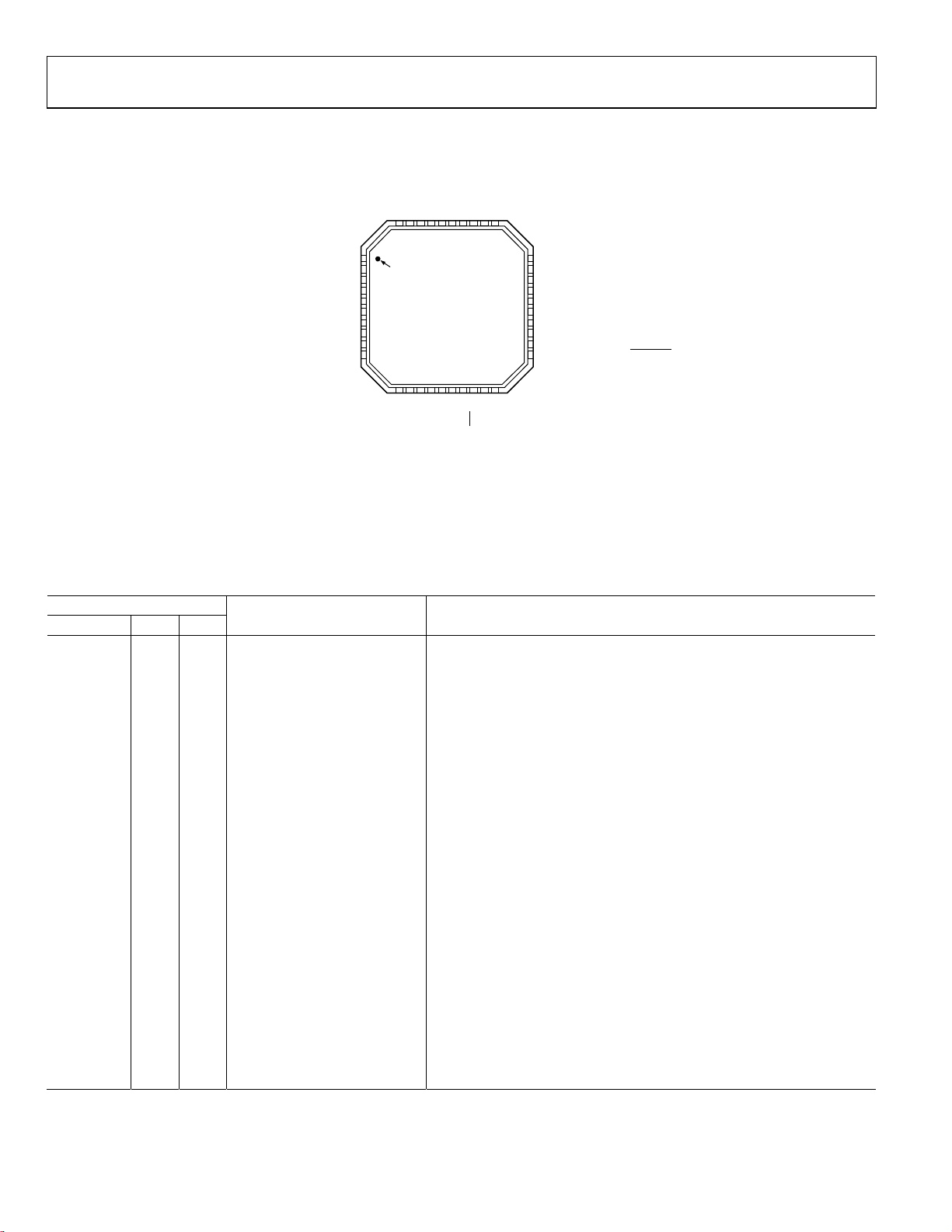
Page 21
ADuC7019/20/21/22/24/25/26/27/28/29
ADuC7024/ADuC7025
REF
REF
64 ADC3/CMP1
63 ADC2/CMP0
62 ADC1
61 ADC0
60 DACVDD59 AVDD58 AGND
57 DACGND
56 DAC
55 V
54 P4.5/PLAO[13]
53 P4.4/PLAO[12]
52 P4.3/PLAO[11]
51 P4.2/PLAO[10]
50 P1 .0/T1/SPM0/PLAI [0]
49 P1 .1/SPM1/PLAI[ 1]
1ADC4
PIN 1
2ADC5
INDICATO R
3ADC6
4ADC7
5ADC8
6ADC9
7GND
REF
8ADCNEG
9DAC0 /ADC12
10DAC 1/ADC13
11TMS
12TDI
13P4.6/PLAO[14]
14P4.7/PLAO[15]
15BM/P0.0/CMP
/PLAI[7]
OUT
NOTES
1. THE EXPOSED PADDLE M UST BE LEFT UNCONNECTED.
Figure 13.
16P0.6/T1/MRST/PLAO[3]
64-Lead LFCSP_VQ Pin Configuration (ADuC7024/ADuC7025)
17TCK
18TDO
19IOGND
20IOVDD21LVDD22DGND
ADuC7024/
ADuC7025
TOP VIEW
(Not to Scale)
26P3.3/PWM1
23P3.0/PWM0
24P3.1/PWM0
25P3.2/PWM1
/PLAI[8]
/PLAI[9]
L
/PLAI[10]
/PLAI[11]
H
L
H
27P0.3/TRST/ADC
BUSY
28
RST
48 P1.2/SPM 2/PLAI[2]
47 P1.3/SPM 3/PLAI[3]
46 P1.4/SPM 4/PLAI[4]/I RQ2
45 P1.5/SPM 5/PLAI[5]/I RQ3
44 P4.1/PLAO[9]
43 P4.0/PLAO[8]
42 I OV
DD
41 I OGND
40 P1.6/SPM 6/PLAI[6]
39 P1.7/SPM 7/PLAO[0]
38 P3.7/PWM
37 P3.6/PWM
36 XCLKI
35 XCLKO
34 P0.7/ECLK/XCLK/SPM8/PLAO[4]
33 P2.0/SPM 9/PLAO[5]/CONV
30P3.5/PWM2
31IRQ0/P0.4/PWM
32IRQ1/P0.5/ADC
29P3.4/PWM2
/PLAO[1]
/PLAO[2]
/PLAI[12]
/PLAI[13]
L
H
TRIP
BUSY
SYNC
TRIP
/PLAI[15]
/PLAI[14]
START
04955-067
DD
REF
REF
64 ADC3/CMP1
63 ADC2/CMP0
62 ADC1
61 ADC0
60 DACV
59 AVDD58 AGND
57 DACGND
56 DAC
55 V
54 P4.5/PLAO[13]
53 P4.4/PLAO[12]
52 P4.3/PLAO[11]
51 P4.2/PLAO[10]
50 P1. 0/T1/SPM0/PLAI[ 0]
49 P1. 1/SPM1/PLAI[1]
48 P1 .2/SPM2/PLAI[ 2]
47 P1 .3/SPM3/PLAI[ 3]
46 P1.4/SPM4/PLAI[4]/IRQ2
45 P1.5/SPM5/PLAI[5]/IRQ3
44 P4.1/PLAO[9]
43 P4.0/PLAO[8]
42 IO V
DD
41 IO GND
40 P1 .6/SPM6/PLAI[ 6]
39 P1 .7/SPM7/PLAO[ 0]
38 P3.7/PWM
37 P3.6/PWM
36 XCLKI
35 XCLKO
34 P0 .7/ECLK/XCLK/SPM8/ PLAO[4]
33 P2 .0/SPM9/PLAO[ 5]/CONV
32IRQ1/P0.5/ADC
30P3.5/PWM2
31IRQ0/P0.4/PWM
/PLAO[1]
/PLAO[2]
/PLAI[13]
L
TRIP
BUSY
SYNC
TRIP
/PLAI[15]
/PLAI[14]
OUT
REF
/PLAI[7]
1ADC4
PIN 1
2ADC5
INDICATO R
3ADC6
4ADC7
5ADC8
6ADC9
7GND
8ADCNEG
9DAC0/ADC12
10DAC1/ADC13
11TMS
12TDI
13P4.6/PLAO[14]
14P4.7/PLAO[15]
15BM/P0.0/CMP
16P0.6/T1/MRST/PLAO[3]
17TCK
18TDO
19IOGND
ADuC7024/
ADuC7025
TOP VIEW
(Not to Scale)
20IOVDD21LVDD22DGND
23P3.0/PWM 0
24P3.1/PWM0
25P3.2/PWM1
/PLAI[8]
/PLAI[9]
L
/PLAI[10]
H
H
26P3.3/PWM1
27P0. 3/TRST/ADC
28
29P3.4/PWM2
RST
BUSY
/PLAI[11]
/PLAI[12]
L
H
Figure 14. 64-Lead LQFP Pin Configuration (ADuC7024/ADuC7025)
START
04955-068
Rev. D | Page 21 of 96
Page 22

ADuC7019/20/21/22/24/25/26/27/28/29
Table 12. Pin Function Descriptions (ADuC7024/ADuC7025 64-Lead LFCSP_VQ and 64-Lead LQFP)
Pin No. Mnemonic Description
1 ADC4 Single-Ended or Differential Analog Input 4.
2 ADC5 Single-Ended or Differential Analog Input 5.
3 ADC6 Single-Ended or Differential Analog Input 6.
4 ADC7 Single-Ended or Differential Analog Input 7.
5 ADC8 Single-Ended or Differential Analog Input 8.
6 ADC9 Single-Ended or Differential Analog Input 9.
7 GND
8 ADCNEG
9 DAC0/ADC12
10 DAC1/ADC13
11 TMS JTAG Test Port Input, Test Mode Select. Debug and download access.
12 TDI JTAG Test Port Input, Test Data In. Debug and download access
13 P4.6/PLAO[14] General-Purpose Input and Output Port 4.6/Programmable Logic Array Output Element 14.
14 P4.7/PLAO[15] General-Purpose Input and Output Port 4.7/Programmable Logic Array Output Element 15.
15 BM/P0.0/CMP
16 P0.6/T1/MRST/PLAO[3]
17 TCK JTAG Test Port Input, Test Clock. Debug and download access.
18 TDO JTAG Test Port Output, Test Data Out. Debug and download access.
19 IOGND Ground for GPIO (see Table 7 8). Typically connected to DGND.
20 IOVDD 3.3 V Supply for GPIO (see Tab le 78) and Input of the On-Chip Voltage Regulator.
21 LVDD
22 DGND Ground for Core Logic.
23 P3.0/PWM0H/PLAI[8]
24 P3.1/PWM0L/PLAI[9]
25 P3.2/PWM1H/PLAI[10]
26 P3.3/PWM1L/PLAI[11]
27 P0.3/TRST/ADC
28
29 P3.4/PWM2H/PLAI[12]
30 P3.5/PWM2L/PLAI[13]
31 IRQ0/P0.4/PWM
32 IRQ1/P0.5/ADC
33
34 P0.7/ECLK/XCLK/SPM8/PLAO[4]
35 XCLKO Output from the Crystal Oscillator Inverter.
36 XCLKI Input to the Crystal Oscillator Inverter and Input to the Internal Clock Generator Circuits.
REF
/PLAI[7]
OUT
General-Purpose Input and Output Port 0.3/JTAG Test Port Input, Test Reset/ADC
BUSY
RST
/PLAO[1]
TRIP
/PLAO[2]
BUSY
P2.0/SPM9/PLAO[5]/CONV
Ground Voltage Reference for the ADC. For optimal performance, the analog power supply
should be separated from IOGND and DGND.
Bias Point or Negative Analog Input of the ADC in Pseudo Differential Mode. Must be connected
to the ground of the signal to convert. This bias point must be between 0 V and 1 V.
DAC0 Voltage Output/Single-Ended or Differential Analog Input 12. DAC outputs are not present
on the ADuC7025.
DAC1 Voltage Output/Single-Ended or Differential Analog Input 13. DAC outputs are not present
on the ADuC7025.
Multifunction I/O Pin. Boot mode. The ADuC7024/ADuC7025 enter download mode if BM is low at
reset and execute code if BM is pulled high at reset through a 1 kΩ resistor/General-Purpose Input
and Output Port 0.0/Voltage Comparator Output/Programmable Logic Array Input Element 7.
Multifunction Pin, Driven Low After Reset. General-Purpose Output Port 0.6/Timer1 Input/PowerOn Reset Output/Programmable Logic Array Output Element 3.
2.6 V Output of the On-Chip Voltage Regulator. This output must be connected to a 0.47 µF
capacitor to DGND only.
General-Purpose Input and Output Port 3.0/PWM Phase 0 High-Side Output/Programmable Logic
Array Input Element 8.
General-Purpose Input and Output Port 3.1/PWM Phase 0 Low-Side Output/Programmable Logic
Array Input Element 9.
General-Purpose Input and Output Port 3.2/PWM Phase 1 High-Side Output/Programmable Logic
Array Input Element 10.
General-Purpose Input and Output Port 3.3/PWM Phase 1 Low-Side Output/Programmable Logic
Array Input Element 11.
Signal Output.
BUSY
Reset Input, Active Low.
General-Purpose Input and Output Port 3.4/PWM Phase 2 High-Side Output/Programmable Logic
Array Input 12.
General-Purpose Input and Output Port 3.5/PWM Phase 2 Low-Side Output/Programmable Logic
Array Input Element 13.
Multifunction I/O Pin. External Interrupt Request 0, Active High/General-Purpose Input and
Output Port 0.4/PWM Trip External Input/Programmable Logic Array Output Element 1.
Multifunction I/O Pin. External Interrupt Request 1, Active High/General-Purpose Input and
Output Port 0.5/ADC
Serial Port Multiplexed. General-Purpose Input and Output Port 2.0/UART/Programmable Logic
START
Signal Output/Programmable Logic Array Output Element 2.
BUSY
Array Output Element 5/Start Conversion Input Signal for ADC.
Serial Port Multiplexed. General-Purpose Input and Output Port 0.7/Output for External Clock
Signal/Input to the Internal Clock Generator Circuits/UART/Programmable Logic Array Output
Element 4.
Rev. D | Page 22 of 96
Page 23

ADuC7019/20/21/22/24/25/26/27/28/29
Pin No. Mnemonic Description
37 P3.6/PWM
38 P3.7/PWM
39 P1.7/SPM7/PLAO[0]
40 P1.6/SPM6/PLAI[6]
41 IOGND Ground for GPIO (see Table 7 8). Typically connected to DGND.
42 IOVDD 3.3 V Supply for GPIO (see Tab le 78) and Input of the On-Chip Voltage Regulator.
43 P4.0/PLAO[8] General-Purpose Input and Output Port 4.0/Programmable Logic Array Output Element 8.
44 P4.1/PLAO[9] General-Purpose Input and Output Port 4.1/Programmable Logic Array Output Element 9.
45 P1.5/SPM5/PLAI[5]/IRQ3
46 P1.4/SPM4/PLAI[4]/IRQ2
47 P1.3/SPM3/PLAI[3]
48 P1.2/SPM2/PLAI[2]
49 P1.1/SPM1/PLAI[1]
50 P1.0/T1/SPM0/PLAI[0]
51 P4.2/PLAO[10] General-Purpose Input and Output Port 4.2/Programmable Logic Array Output Element 10.
52 P4.3/PLAO[11] General-Purpose Input and Output Port 4.3/Programmable Logic Array Output Element 11.
53 P4.4/PLAO[12] General-Purpose Input and Output Port 4.4/Programmable Logic Array Output Element 12.
54 P4.5/PLAO[13] General-Purpose Input and Output Port 4.5/Programmable Logic Array Output Element 13.
55 V
56 DAC
REF
REF
57 DACGND Ground for the DAC. Typically connected to AGND.
58 AGND Analog Ground. Ground reference point for the analog circuitry.
59 AVDD 3.3 V Analog Power.
60 DACVDD 3.3 V Power Supply for the DACs. Must be connected to AVDD.
61 ADC0 Single-Ended or Differential Analog Input 0.
62 ADC1 Single-Ended or Differential Analog Input 1.
63 ADC2/CMP0 Single-Ended or Differential Analog Input 2/Comparator Positive Input.
64 ADC3/CMP1 Single-Ended or Differential Analog Input 3/Comparator Negative Input.
0 EP
/PLAI[14]
TRIP
General-Purpose Input and Output Port 3.6/PWM Safety Cutoff/Programmable Logic Array Input
Element 14.
/PLAI[15]
SYNC
General-Purpose Input and Output Port 3.7/PWM Synchronization Input and Output/
Programmable Logic Array Input Element 15.
Serial Port Multiplexed. General-Purpose Input and Output Port 1.7/UART, SPI/Programmable
Logic Array Output Element 0.
Serial Port Multiplexed. General-Purpose Input and Output Port 1.6/UART, SPI/Programmable
Logic Array Input Element 6.
Serial Port Multiplexed. General-Purpose Input and Output Port 1.5/UART, SPI/Programmable
Logic Array Input Element 5/External Interrupt Request 3, Active High.
Serial Port Multiplexed. General-Purpose Input and Output Port 1.4/UART, SPI/Programmable
Logic Array Input Element 4/External Interrupt Request 2, Active High.
Serial Port Multiplexed. General-Purpose Input and Output Port 1.3/UART, I2C1/Programmable
Logic Array Input Element 3.
Serial Port Multiplexed. General-Purpose Input and Output Port 1.2/UART, I2C1/Programmable
Logic Array Input Element 2.
Serial Port Multiplexed. General-Purpose Input and Output Port 1.1/UART, I2C0/Programmable Logic
Array Input Element 1.
Serial Port Multiplexed. General-Purpose Input and Output Port 1.0/Timer1 Input/UART, I2C0/
Programmable Logic Array Input Element 0.
2.5 V Internal Voltage Reference. Must be connected to a 0.47 µF capacitor when using the
internal reference.
External Voltage Reference for the DACs. Range: DACGND to DACVDD.
Exposed Paddle. The pin configuration for the ADuC7024/ADuC7025 LFCSP_VQ has an exposed
paddle that must be left unconnected.
Rev. D | Page 23 of 96
Page 24
ADuC7019/20/21/22/24/25/26/27/28/29
ADuC7026/ADuC7027
/PLAI[7]/MS0
OUT
H
REF
/BLE
DD
78 ADC1
77 ADC0
23TDO
24P0.2/PWM2
/BHE
L
74 AVDD73 AVDD72 AGND
76 ADC11
75 DACV
ADuC7026/
ADuC7027
(Not to Scale)
25IOGND
26IOV
27LVDD28DGND
DD
80 ADC3/CMP1
79 ADC2/CMP0
1ADC4
2ADC5
3ADC6
4ADC7
5ADC8
6ADC9
7ADC10
8GND
9ADCNEG
10DAC0/ADC12
11DAC1/ADC13
12DAC2/ADC14
13DAC3/ADC15
14TMS
15TDI
16P0.1/PWM2
17P2.3/AE
18P4.6/AD14/PLAO[14]
19P4.7/AD15/PLAO[15]
20BM/P0.0/ CMP
PIN 1
INDICATO R
21P0.6/T1/MRST/PLAO[3]
22TCK
71 AGND
70 DACGND
TOP VIEW
30P3.1/AD1/PWM0
31P3.2/AD2/PWM1
29P3.0/AD0/PWM0
/PLAI[8]
/PLAI[9]
L
/PLAI[10]
H
H
REF
69 DAC
32P3.3/AD3/PWM1
/PLAI[11]
L
REF
68 V
67 REFGND
66 P4.5/ AD13/PLAO[13]
65 P4.4/ AD12/PLAO[12]
64 P4.3/ AD11/PLAO[11]
63 P4.2/ AD10/PLAO[10]
62 P1.0/T1/SPM0/PLAI[0]
61 P1.1/SPM1/PL AI[1]
60 P1.2/SPM2/PLAI[2]
59 P1.3/SPM3/PLAI[3]
58 P1.4/SPM4/PLAI[4]/IRQ2
57 P1.5/SPM5/PLAI[5]/IRQ3
56 P4.1/AD9/PLAO[9]
55 P4.0/AD8/PLAO[8]
54 IOV
DD
53 IOGND
52 P1.6/SPM6/PLAI[6]
51 P1.7/SPM7/PLAO[0]
50 P2.2/RS/PWM0
49 P2.1/WS/PWM0
48 P2.7/PWM1
47 P3.7/AD7/PWM
46 P3.6/AD6/PWM
45 XCLKI
44 XCLKO
43 P0.7/ECLK/XCLK/SPM8/PLAO[4]
42 P2.0/SPM9/PLAO[5]/CONV
41 IRQ1/P0.5/ADC
34P0.3/TRS T/A16/ADC
36P2.6/PWM1
37RST
38P3.4/AD4/PWM2
35P2.5/PWM0
33P2.4/PWM0
BUSY
/MS0
H
39P3.5/AD5/PWM2
40IRQ0/P0.4/P WM
/MS1
/MS2
L
H
/PLAI[12]
/PLAI[13]
L
H
/PLAO[1]/MS1
TRIP
/MS3
L
/PLAO[7]
L
/PLAO[6]
H
/PLAI[15]
SYNC
/PLAI[14]
TRIP
/PLAO[2]/MS2
BUSY
START
Figure 15. 80-Lead LQFP Pin Configuration (ADuC7026/ADuC7027)
Table 13. Pin Function Descriptions (ADuC7026/ADuC7027)
Pin No. Mnemonic Description
1 ADC4 Single-Ended or Differential Analog Input 4.
2 ADC5 Single-Ended or Differential Analog Input 5.
3 ADC6 Single-Ended or Differential Analog Input 6.
4 ADC7 Single-Ended or Differential Analog Input 7.
5 ADC8 Single-Ended or Differential Analog Input 8.
6 ADC9 Single-Ended or Differential Analog Input 9.
7 ADC10 Single-Ended or Differential Analog Input 10.
8 GND
REF
Ground Voltage Reference for the ADC. For optimal performance, the analog power supply
should be separated from IOGND and DGND.
9 ADCNEG
Bias Point or Negative Analog Input of the ADC in Pseudo Differential Mode. Must be connected
to the ground of the signal to convert. This bias point must be between 0 V and 1 V.
10 DAC0/ADC12
DAC0 Voltage Output/Single-Ended or Differential Analog Input 12. DAC outputs are not
present on the ADuC7027.
11 DAC1/ADC13
DAC1 Voltage Output/Single-Ended or Differential Analog Input 13. DAC outputs are not
present on the ADuC7027.
12 DAC2/ADC14
DAC2 Voltage Output/Single-Ended or Differential Analog Input 14. DAC outputs are not
present on the ADuC7027.
13 DAC3/ADC15
DAC3 Voltage Output/Single-Ended or Differential Analog Input 15. DAC outputs are not
present on the ADuC7027.
14 TMS JTAG Test Port Input, Test Mode Select. Debug and download access.
Rev. D | Page 24 of 96
04955-069
Page 25
ADuC7019/20/21/22/24/25/26/27/28/29
Pin No. Mnemonic Description
15 TDI JTAG Test Port Input, Test Data In. Debug and download access.
16
P0.1/PWM2
17 P2.3/AE General-Purpose Input and Output Port 2.3/External Memory Access Enable.
18 P4.6/AD14/PLAO[14]
19 P4.7/AD15/PLAO[15]
20 BM/P0.0/CMP
21 P0.6/T1/MRST/PLAO[3]
22 TCK JTAG Test Port Input, Test Clock. Debug and download access.
23 TDO JTAG Test Port Output, Test Data Out. Debug and download access.
24
P0.2/PWM2
25 IOGND Ground for GPIO (see Table 78). Typically connected to DGND.
26 IOVDD 3.3 V Supply for GPIO (see Table 7 8) and Input of the On-Chip Voltage Regulator.
27 LVDD
28 DGND Ground for Core Logic.
29 P3.0/AD0/PWM0H/PLAI[8]
30 P3.1/AD1/PWM0L/PLAI[9]
31 P3.2/AD2/PWM1H/PLAI[10]
32 P3.3/AD3/PWM1L/PLAI[11]
33 P2.4/PWM0H/MS0
34 P0.3/TRST/A16/ADC
35 P2.5/PWM0L/MS1
36 P2.6/PWM1H/MS2
37
RST
38 P3.4/AD4/PWM2H/PLAI[12]
39 P3.5/AD5/PWM2L/PLAI[13]
40 IRQ0/P0.4/PWM
41 IRQ1/P0.5/ADC
42
P2.0/SPM9/PLAO[5]/
43 P0.7/ECLK/XCLK/SPM8/PLAO[4]
44 XCLKO Output from the Crystal Oscillator Inverter.
45 XCLKI Input to the Crystal Oscillator Inverter and Input to the Internal Clock Generator Circuits.
/BLE General-Purpose Input and Output Port 0.1/PWM Phase 2 High-Side Output/External Memory
H
Byte Low Enable.
General-Purpose Input and Output Port 4.6/External Memory Interface/Programmable Logic
Array Output Element 14.
General-Purpose Input and Output Port 4.7/External Memory Interface/Programmable Logic
Array Output Element 15.
/PLAI[7]/MS0
OUT
Multifunction I/O Pin. Boot Mode. The ADuC7026/ADuC7027 enter UART download mode if BM
is low at reset and execute code if BM is pulled high at reset through a 1 kΩ resistor/GeneralPurpose Input and Output Port 0.0/Voltage Comparator Output/Programmable Logic Array
Input Element 7/External Memory Select 0.
Multifunction Pin, Driven Low After Reset. General-Purpose Output Port 0.6/Timer1 Input/
Power-On Reset Output/Programmable Logic Array Output Element 3.
/BHE General-Purpose Input and Output Port 0.2/PWM Phase 2 Low-Side Output/External Memory
L
Byte High Enable.
2.6 V Output of the On-Chip Voltage Regulator. This output must be connected to a 0.47 µF
capacitor to DGND only.
General-Purpose Input and Output Port 3.0/External Memory Interface/PWM Phase 0 High-Side
Output/Programmable Logic Array Input Element 8.
General-Purpose Input and Output Port 3.1/External Memory Interface/PWM Phase 0 Low-Side
Output/Programmable Logic Array Input Element 9.
General-Purpose Input and Output Port 3.2/External Memory Interface/PWM Phase 1 High-Side
Output/Programmable Logic Array Input Element 10.
General-Purpose Input and Output Port 3.3/External Memory Interface/PWM Phase 1 Low-Side
Output/Programmable Logic Array Input Element 11.
General-Purpose Input and Output Port 2.4/PWM Phase 0 High-Side Output/External Memory
Select 0.
General-Purpose Input and Output Port 0.3/JTAG Test Port Input, Test Reset/ADC
BUSY
Signal Output.
BUSY
General-Purpose Input and Output Port 2.5/PWM Phase 0 Low-Side Output/External Memory
Select 1.
General-Purpose Input and Output Port 2.6/PWM Phase 1 High-Side Output/External Memory
Select 2.
Reset Input, Active Low.
General-Purpose Input and Output Port 3.4/External Memory Interface/PWM Phase 2 High-Side
Output/Programmable Logic Array Input 12.
General-Purpose Input and Output Port 3.5/External Memory Interface/PWM Phase 2 Low-Side
Output/Programmable Logic Array Input Element 13.
/PLAO[1]/MS1
TRIP
Multifunction I/O Pin. External Interrupt Request 0, Active High/General-Purpose Input and
Output Port 0.4/PWM Trip External Input/Programmable Logic Array Output Element 1/
External Memory Select 1.
/PLAO[2]/MS2
BUSY
Multifunction I/O Pin. External Interrupt Request 1, Active High/General-Purpose Input and
Output Port 0.5/ADC
Signal Output/Programmable Logic Array Output Element 2/External
BUSY
Memory Select 2.
CONV
Serial Port Multiplexed. General-Purpose Input and Output Port 2.0/UART/Programmable Logic
START
Array Output Element 5/Start Conversion Input Signal for ADC.
Serial Port Multiplexed. General-Purpose Input and Output Port 0.7/Output for External Clock
Signal/Input to the Internal Clock Generator Circuits/UART/Programmable Logic Array Output
Element 4.
Rev. D | Page 25 of 96
Page 26

ADuC7019/20/21/22/24/25/26/27/28/29
Pin No. Mnemonic Description
46 P3.6/AD6/PWM
47 P3.7/AD7/PWM
48 P2.7/PWM1L/MS3
49
50
P2.1/WS
P2.2/RS
/PWM0H/PLAO[6] General-Purpose Input and Output Port 2.1/External Memory Write Strobe/PWM Phase 0 High-
/PWM0L/PLAO[7] General-Purpose Input and Output Port 2.2/External Memory Read Strobe/PWM Phase 0 Low-
51 P1.7/SPM7/PLAO[0]
52 P1.6/SPM6/PLAI[6]
53 IOGND Ground for GPIO (see Table 78). Typically connected to DGND.
54 IOVDD 3.3 V Supply for GPIO (see Table 7 8) and Input of the On-Chip Voltage Regulator.
55 P4.0/AD8/PLAO[8]
56 P4.1/AD9/PLAO[9]
57 P1.5/SPM5/PLAI[5]/IRQ3
58 P1.4/SPM4/PLAI[4]/IRQ2
59 P1.3/SPM3/PLAI[3]
60 P1.2/SPM2/PLAI[2]
61 P1.1/SPM1/PLAI[1]
62 P1.0/T1/SPM0/PLAI[0]
63 P4.2/AD10/PLAO[10]
64 P4.3/AD11/PLAO[11]
65 P4.4/AD12/PLAO[12]
66 P4.5/AD13/PLAO[13]
67 REFGND Ground for the Reference. Typically connected to AGND.
68 V
69 DAC
REF
External Voltage Reference for the DACs. Range: DACGND to DACVDD.
REF
70 DACGND Ground for the DAC. Typically connected to AGND.
71, 72 AGND Analog Ground. Ground reference point for the analog circuitry.
73, 74 AVDD 3.3 V Analog Power.
75 DACVDD 3.3 V Power Supply for the DACs. Must be connected to AVDD.
76 ADC11 Single-Ended or Differential Analog Input 11.
77 ADC0 Single-Ended or Differential Analog Input 0.
78 ADC1 Single-Ended or Differential Analog Input 1.
79 ADC2/CMP0 Single-Ended or Differential Analog Input 2/Comparator Positive Input.
80 ADC3/CMP1 Single-Ended or Differential Analog Input 3/Comparator Negative Input.
/PLAI[14]
TRIP
/PLAI[15]
SYNC
General-Purpose Input and Output Port 3.6/External Memory Interface/PWM Safety Cutoff/
Programmable Logic Array Input Element 14.
General-Purpose Input and Output Port 3.7/External Memory Interface/PWM Synchronization/
Programmable Logic Array Input Element 15.
General-Purpose Input and Output Port 2.7/PWM Phase 1 Low-Side Output/External Memory
Select 3.
Side Output/Programmable Logic Array Output Element 6.
Side Output/Programmable Logic Array Output Element 7.
Serial Port Multiplexed. General-Purpose Input and Output Port 1.7/UART, SPI/Programmable Logic
Array Output Element 0.
Serial Port Multiplexed. General-Purpose Input and Output Port 1.6/UART, SPI/Programmable Logic
Array Input Element 6.
General-Purpose Input and Output Port 4.0/External Memory Interface/Programmable Logic
Array Output Element 8.
General-Purpose Input and Output Port 4.1/External Memory Interface/Programmable Logic
Array Output Element 9.
Serial Port Multiplexed. General-Purpose Input and Output Port 1.5/UART, SPI/Programmable Logic
Array Input Element 5/External Interrupt Request 3, Active High.
Serial Port Multiplexed. General-Purpose Input and Output Port 1.4/UART, SPI/Programmable Logic
Array Input Element 4/External Interrupt Request 2, Active High.
Serial Port Multiplexed. General-Purpose Input and Output Port 1.3/UART, I2C1/Programmable
Logic Array Input Element 3.
Serial Port Multiplexed. General-Purpose Input and Output Port 1.2/UART, I2C1/Programmable
Logic Array Input Element 2.
Serial Port Multiplexed. General-Purpose Input and Output Port 1.1/UART, I2C0/Programmable
Logic Array Input Element 1.
Serial Port Multiplexed. General-Purpose Input and Output Port 1.0/Timer1 Input/UART, I2C0/
Programmable Logic Array Input Element 0.
General-Purpose Input and Output Port 4.2/External Memory Interface/Programmable Logic
Array Output Element 10.
General-Purpose Input and Output Port 4.3/External Memory Interface/Programmable Logic
Array Output Element 11.
General-Purpose Input and Output Port 4.4/External Memory Interface/Programmable Logic
Array Output Element 12.
General-Purpose Input and Output Port 4.5/External Memory Interface/Programmable Logic
Array Output Element 13.
2.5 V Internal Voltage Reference. Must be connected to a 0.47 µF capacitor when using the
internal reference.
Rev. D | Page 26 of 96
Page 27
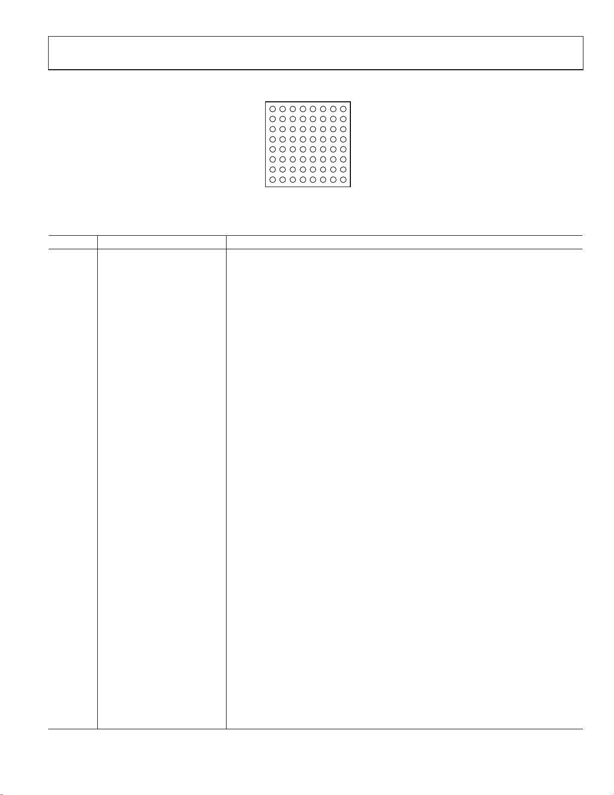
ADuC7019/20/21/22/24/25/26/27/28/29
ADUC7028
87654321
A
B
C
D
E
F
G
H
BOTTOM VIEW
(Not to Scale)
Figure 16. 64-Ball BGA Pin Configuration (ADuC7028)
Table 14. Pin Function Descriptions (ADuC7028)
Ball No. Mnemonic Description
A1 ADC3/CMP1 Single-Ended or Differential Analog Input 3/Comparator Negative Input.
A2 DACVDD 3.3 V Power Supply for the DACs. Must be connected to AVDD.
A3 AVDD 3.3 V Analog Power.
A4 AGND Analog Ground. Ground reference point for the analog circuitry.
A5 DACGND Ground for the DAC. Typically connected to AGND.
A6 P4.2/PLAO[10] General-Purpose Input and Output Port 4.2/Programmable Logic Array Output Element 10.
A7 P1.1/SPM1/PLAI[1]
Serial Port Multiplexed. General-Purpose Input and Output Port 1.1/UART, I2C0/Programmable
Logic Array Input Element 1.
A8 P1.2/SPM2/PLAI[2]
Serial Port Multiplexed. General-Purpose Input and Output Port 1.2/UART, I2C1/Programmable
Logic Array Input Element 2.
B1 ADC4 Single-Ended or Differential Analog Input 4.
B2 ADC2/CMP0 Single-Ended or Differential Analog Input 2/Comparator Positive Input.
B3 ADC1 Single-Ended or Differential Analog Input 1.
B4 DAC
B5 V
External Voltage Reference for the DACs. Range: DACGND to DACVDD.
REF
REF
2.5 V Internal Voltage Reference. Must be connected to a 0.47 µF capacitor when using the
internal reference.
B6 P1.0/T1/SPM0/PLAI[0]
Serial Port Multiplexed. General-Purpose Input and Output Port 1.0/Timer1 Input/UART, I2C0/
Programmable Logic Array Input Element 0.
B7 P1.4/SPM4/PLAI[4]/IRQ2
Serial Port Multiplexed. General-Purpose Input and Output Port 1.4/UART, SPI/Programmable
Logic Array Input Element 4/External Interrupt Request 2, Active High.
B8 P1.3/SPM3/PLAI[3]
Serial Port Multiplexed. General-Purpose Input and Output Port 1.3/UART, I2C1/Programmable
Logic Array Input Element 3.
C1 ADC6 Single-Ended or Differential Analog Input 6.
C2 ADC5 Single-Ended or Differential Analog Input 5.
C3 ADC0 Single-Ended or Differential Analog Input 0.
C4 P4.5/PLAO[13] General-Purpose Input and Output Port 4.5/Programmable Logic Array Output Element 13.
C5 P4.3/PLAO[11] General-Purpose Input and Output Port 4.3/Programmable Logic Array Output Element 11.
C6 P4.0/PLAO[8] General-Purpose Input and Output Port 4.0/Programmable Logic Array Output Element 8.
C7 P4.1/PLAO[9] General-Purpose Input and Output Port 4.1/Programmable Logic Array Output Element 9.
C8 IOGND Ground for GPIO (see Tabl e 78). Typically connected to DGND.
D1 ADCNEG
Bias Point or Negative Analog Input of the ADC in Pseudo Differential Mode. Must be
connected to the ground of the signal to convert. This bias point must be between 0 V and 1 V.
D2 GND
REF
Ground Voltage Reference for the ADC. For optimal performance, the analog power supply
should be separated from IOGND and DGND.
D3 ADC7 Single-Ended or Differential Analog Input 7.
D4 P4.4/PLAO[12] General-Purpose Input and Output Port 4.4/Programmable Logic Array Output Element 12.
D5 P3.6/PWM
/PLAI[14]
TRIP
General-Purpose Input and Output Port 3.6/PWM Safety Cutoff/Programmable Logic Array
Input Element 14.
D6 P1.7/SPM7/PLAO[0]
Serial Port Multiplexed. General-Purpose Input and Output Port 1.7/UART, SPI/Programmable
Logic Array Output Element 0.
04955-086
Rev. D | Page 27 of 96
Page 28

ADuC7019/20/21/22/24/25/26/27/28/29
Ball No. Mnemonic Description
D7 P1.6/SPM6/PLAI[6]
D8 IOVDD 3.3 V Supply for GPIO (see Table 7 8) and Input of the On-Chip Voltage Regulator.
E1 DAC3 DAC3 Voltage Output.
E2 DAC2 DAC2 Voltage Output.
E3 DAC1 DAC1 Voltage Output.
E4 P3.0/PWM0H/PLAI[8]
E5 P3.2/PWM1H/PLAI[10]
E6 P1.5/SPM5/PLAI[5]/IRQ3
E7 P3.7/PWM
/PLAI[15]
SYNC
E8 XCLKI Input to the Crystal Oscillator Inverter and Input to the Internal Clock Generator Circuits.
F1 P4.6/PLAO[14] General-Purpose Input and Output Port 4.6/Programmable Logic Array Output Element 14.
F2 TDI JTAG Test Port Input, Test Data In. Debug and download access.
F3 DAC0s DAC0 Voltage Output.
F4 P3.1/PWM0L/PLAI[9]
F5 P3.3/PWM1L/PLAI[11]
F6
RST
F7 P0.7/ECLK/XCLK/SPM8/PLAO[4]
F8 XCLKO Output from the Crystal Oscillator Inverter.
G1 BM/P0.0/CMP
/PLAI[7]
OUT
G2 P4.7/PLAO[15] General-Purpose Input and Output Port 4.7/Programmable Logic Array Output Element 15.
G3 TMS JTAG Test Port Input, Test Mode Select. Debug and download access.
G4 TDO JTAG Test Port Output, Test Data Out. Debug and download access.
G5 P0.3/TRST/ADC
BUSY
G6 P3.4/PWM2H/PLAI[12]
G7 P3.5/PWM2L/PLAI[13]
G8
P2.0/SPM9/PLAO[5]/CONV
START
H1 P0.6/T1/MRST/PLAO[3]
H2 TCK JTAG Test Port Input, Test Clock. Debug and download access.
H3 IOGND Ground for GPIO (see Tabl e 78). Typically connected to DGND.
H4 IOVDD 3.3 V Supply for GPIO (see Table 7 8) and Input of the On-Chip Voltage Regulator.
H5 LVDD
H6 DGND Ground for Core Logic.
H7 IRQ0/P0.4/PWM
H8 IRQ1/P0.5/ADC
/PLAO[1]
TRIP
/PLAO[2]
BUSY
Serial Port Multiplexed. General-Purpose Input and Output Port 1.6/UART, SPI/Programmable
Logic Array Input Element 6.
General-Purpose Input and Output Port 3.0/PWM Phase 0 High-Side Output/Programmable
Logic Array Input Element 8.
General-Purpose Input and Output Port 3.2/PWM Phase 1 High-Side Output/Programmable
Logic Array Input Element 10.
Serial Port Multiplexed. General-Purpose Input and Output Port 1.5/UART, SPI/Programmable
Logic Array Input Element 5/External Interrupt Request 3, Active High.
General-Purpose Input and Output Port 3.7/PWM Synchronization/Programmable Logic
Array Input Element 15.
General-Purpose Input and Output Port 3.1/PWM Phase 0 Low-Side Output/Programmable
Logic Array Input Element 9.
General-Purpose Input and Output Port 3.3/PWM Phase 1 Low-Side Output/Programmable
Logic Array Input Element 11.
Reset Input, Active Low.
Serial Port Multiplexed. General-Purpose Input and Output Port 0.7/Output for External
Clock Signal/Input to the Internal Clock Generator Circuits/UART/Programmable Logic Array
Output Element 4.
Multifunction I/O Pin. Boot mode. The ADuC7028 enters UART download mode if BM is low
at reset and executes code if BM is pulled high at reset through a 1 kΩ resistor/GeneralPurpose Input and Output Port 0.0/Voltage Comparator Output/Programmable Logic Array
Input Element 7.
General-Purpose Input and Output Port 0.3/JTAG Test Port Input, Test Reset/ADC
BUSY
Signal
Output.
General-Purpose Input and Output Port 3.4/PWM Phase 2 High-Side Output/Programmable
Logic Array Input 12.
General-Purpose Input and Output Port 3.5/PWM Phase 2 Low-Side Output/Programmable
Logic Array Input Element 13.
Serial Port Multiplexed. General-Purpose Input and Output Port 2.0/UART/Programmable
Logic Array Output Element 5/Start Conversion Input Signal for ADC.
Multifunction Pin, Driven Low After Reset. General-Purpose Output Port 0.6/Timer1 Input/
Power-On Reset Output/Programmable Logic Array Output Element 3.
2.6 V Output of the On-Chip Voltage Regulator. This output must be connected to a 0.47 µF
capacitor to DGND only.
Multifunction I/O Pin. External Interrupt Request 0, Active High/General-Purpose Input and
Output Port 0.4/PWM Trip External Input/Programmable Logic Array Output Element 1.
Multifunction I/O Pin. External Interrupt Request 1, Active High/General-Purpose Input and
Output Port 0.5/ADC
Signal Output/Programmable Logic Array Output Element 2.
BUSY
Rev. D | Page 28 of 96
Page 29
ADuC7019/20/21/22/24/25/26/27/28/29
ADUC7029
Figure 17. 49-Ball BGA Pin Configuration (ADuC7029)
Table 15. Pin Function Descriptions (ADuC7029)
Ball No. Mnemonic Description
A1 ADC3/CMP1 Single-Ended or Differential Analog Input 3/Comparator Negative Input.
A2 ADC1 Single-Ended or Differential Analog Input 1.
A3 ADC0 Single-Ended or Differential Analog Input 0.
A4 AVDD 3.3 V Analog Power.
A5 V
A6 P1.0/T1/SPM0/PLAI[0]
A7 P1.1/SPM1/PLAI[1]
B1 ADC6 Single-Ended or Differential Analog Input 6.
B2 ADC5 Single-Ended or Differential Analog Input 5.
B3 ADC4 Single-Ended or Differential Analog Input 4.
B4 AGND Analog Ground. Ground reference point for the analog circuitry.
B5 DAC
B6 P1.4/SPM4/PLAI[4]/IRQ2
B7 P1.3/SPM3/PLAI[3]
C1 GND
C2 AGND Analog Ground. Ground reference point for the analog circuitry.
C3 ADC2/CMP0 Single-Ended or Differential Analog Input 2/Comparator Positive Input.
C4 IOGND Ground for GPIO (see Tab le 78). Typically connected to DGND.
C5 P1.2/SPM2/PLAI[2]
C6 P1.6/SPM6/PLAI[6]
C7 P1.5/SPM5/PLAI[5]/IRQ3
D1 DAC0 DAC0 Voltage Output.
D2 DAC3 DAC3 Voltage Output.
D3 DAC1 DAC1 Voltage Output.
D4 P3.3/PWM1L/PLAI[11]
D5 P3.4/PWM2H/PLAI[12]
D6 P3.6/PWM
D7 P1.7/SPM7/PLAO[0]
REF
2.5 V Internal Voltage Reference. Must be connected to a 0.47 µF capacitor when using the
internal reference.
Serial Port Multiplexed. General-Purpose Input and Output Port 1.0/Timer1 Input/UART, I2C0/
Programmable Logic Array Input Element 0.
Serial Port Multiplexed. General-Purpose Input and Output Port 1.1/UART, I2C0/Programmable
Logic Array Input Element 1.
External Voltage Reference for the DACs. Range: DACGND to DACVDD.
REF
Serial Port Multiplexed. General-Purpose Input and Output Port 1.4/UART, SPI/Programmable
Logic Array Input Element 4/External Interrupt Request 2, Active High.
Serial Port Multiplexed. General-Purpose Input and Output Port 1.3/UART, I2C1/Programmable
Logic Array Input Element 3.
REF
Ground Voltage Reference for the ADC. For optimal performance, the analog power supply
should be separated from IOGND and DGND.
Serial Port Multiplexed. General-Purpose Input and Output Port 1.2/UART, I2C1/Programmable
Logic Array Input Element 2.
Serial Port Multiplexed. General-Purpose Input and Output Port 1.6/UART, SPI/Programmable
Logic Array Input Element 6.
Serial Port Multiplexed. General-Purpose Input and Output Port 1.5/UART, SPI/Programmable
Logic Array Input Element 5/External Interrupt Request 3, Active High.
General-Purpose Input and Output Port 3.3/PWM Phase 1 Low-Side Output/Programmable
Logic Array Input Element 11.
General-Purpose Input and Output Port 3.4/PWM Phase 2 High-Side Output/Programmable
Logic Array Input 12.
/PLAI[14]
TRIP
General-Purpose Input and Output Port 3.6/PWM Safety Cutoff/Programmable Logic Array
Input Element 14.
Serial Port Multiplexed. General-Purpose Input and Output Port 1.7/UART, SPI/Programmable
Logic Array Output Element 0.
63
745
BOTTOM VIEW
(Not to Scale)
2
1
A
B
C
D
E
F
G
04955-088
Rev. D | Page 29 of 96
Page 30

ADuC7019/20/21/22/24/25/26/27/28/29
Ball No. Mnemonic Description
E1 TMS JTAG Test Port Input, Test Mode Select. Debug and download access.
E2 BM/P0.0/CMP
E3 DAC2 DAC2 Voltage Output.
E4 IOVDD 3.3 V Supply for GPIO (see Table 7 8) and Input of the On-Chip Voltage Regulator.
E5 P3.2/PWM1H/PLAI[10]
E6 P3.5/PWM2L/PLAI[13]
E7 P0.7/ECLK/XCLK/SPM8/PLAO[4]
F1 TDI JTAG Test Port Input, Test Data In. Debug and download access.
F2 P0.6/T1/MRST/PLAO[3]
F3 IOGND Ground for GPIO (see Table 78). Typically connected to DGND.
F4 P3.1/PWM0L/PLAI[9]
F5 P3.0/PWM0H/PLAI[8]
F6
F7
RST
P2.0/SPM9/PLAO[5]/CONV
G1 TCK JTAG Test Port Input, Test Clock. Debug and download access.
G2 TDO JTAG Test Port Output, Test Data Out. Debug and download access.
G3 LVDD
G4 DGND Ground for Core Logic.
G5 P0.3/TRST/ADC
G6 IRQ0/P0.4/PWM
G7 IRQ1/P0.5/ADC
/PLAI[7]
OUT
BUSY
TRIP
BUSY
START
/PLAO[1]
/PLAO[2]
Multifunction I/O Pin. Boot mode. The ADuC7029 enters UART download mode if BM is low
at reset and executes code if BM is pulled high at reset through a 1 kΩ resistor/GeneralPurpose Input and Output Port 0.0/Voltage Comparator Output/Programmable Logic Array
Input Element 7.
General-Purpose Input and Output Port 3.2/PWM Phase 1 High-Side Output/Programmable
Logic Array Input Element 10.
General-Purpose Input and Output Port 3.5/PWM Phase 2 Low-Side Output/Programmable
Logic Array Input Element 13.
Serial Port Multiplexed. General-Purpose Input and Output Port 0.7/Output for External
Clock Signal/Input to the Internal Clock Generator Circuits/UART/Programmable Logic Array
Output Element 4.
Multifunction Pin, Driven Low After Reset. General-Purpose Output Port 0.6/Timer1 Input/
Power-On Reset Output/Programmable Logic Array Output Element 3.
General-Purpose Input and Output Port 3.1/PWM Phase 0 Low-Side Output/Programmable
Logic Array Input Element 9.
General-Purpose Input and Output Port 3.0/PWM Phase 0 High-Side Output/Programmable
Logic Array Input Element 8.
Reset Input, Active Low.
Serial Port Multiplexed. General-Purpose Input and Output Port 2.0/UART/Programmable
Logic Array Output Element 5/Start Conversion Input Signal for ADC.
2.6 V Output of the On-Chip Voltage Regulator. This output must be connected to a 0.47 µF
capacitor to DGND only.
General-Purpose Input and Output Port 0.3/JTAG Test Port Input, Test Reset/ADC
Output.
Multifunction I/O Pin. External Interrupt Request 0, Active High/General-Purpose Input and
Output Port 0.4/PWM Trip External Input/Programmable Logic Array Output Element 1.
Multifunction I/O Pin. External Interrupt Request 1, Active High/General-Purpose Input and
Output Port 0.5/ADC
Signal Output/Programmable Logic Array Output Element 2.
BUSY
BUSY
Signal
Rev. D | Page 30 of 96
Page 31
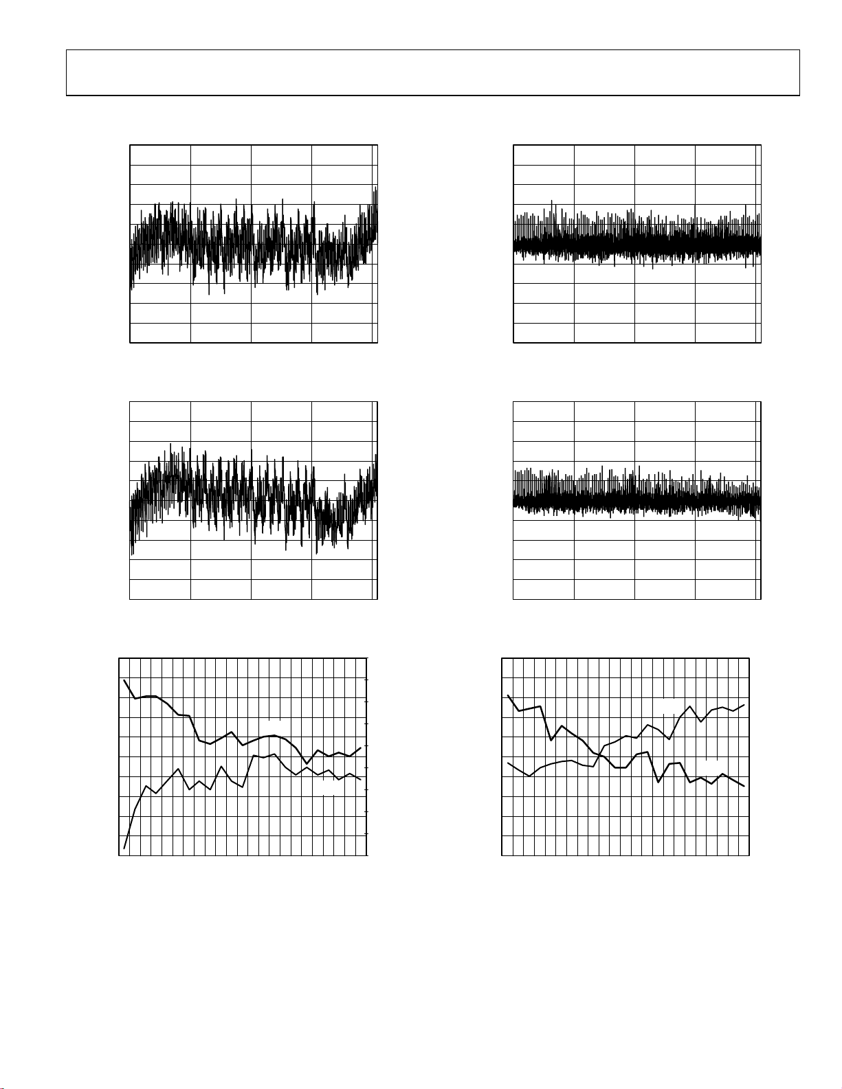
ADuC7019/20/21/22/24/25/26/27/28/29
TYPICAL PERFORMANCE CHARACTERISTICS
1.0
f
= 774kSPS
S
0.8
0.6
0.4
0.2
0
(LSB)
–0.2
–0.4
–0.6
–0.8
–1.0
020001000 3000 4000
Figure 18. Typical INL Error, f
1.0
f
= 1MSPS
S
0.8
0.6
0.4
0.2
0
(LSB)
–0.2
–0.4
–0.6
–0.8
–1.0
0 20001000 3000 4000
Figure 19. Typical INL Error, f
1.0
0.9
0.8
0.7
0.6
0.5
(LSB)
0.4
0.3
0.2
0.1
0
1.0 1.5 2.0 2.5 3.0
EXTERNAL REFERENCE (V)
ADC CODES
ADC CODES
WCP
= 774 kSPS
S
= 1 MSPS
S
WCN
Figure 20. Typical Worst-Case (Positive (WCP) and Negative (WCN))
INL Error vs. V
, fS = 774 kSPS
REF
0
–0.1
–0.2
–0.3
–0.5
–0.6
–0.7
–0.8
–0.9
–1.0
04955-075
04955-077
(LSB)
04955-072
1.0
f
= 774kSPS
S
0.8
0.6
0.4
0.2
0
(LSB)
–0.2
–0.4
–0.6
–0.8
–1.0
020001000 3000 4000
Figure 21. Typical DNL Error, f
1.0
f
= 1MSPS
S
0.8
0.6
0.4
0.2
0
(LSB)
–0.2
–0.4
–0.6
–0.8
–1.0
0 20001000 3000 4000
Figure 22. Typical DNL Error, f
0
–0.1
–0.2
–0.3
–0.4
–0.5
(LSB)
–0.6
–0.7
–0.8
–0.9
–1.0
1.0 1.5 2.0 2.5 3.0
EXTERNAL REFERENCE (V)
ADC CODES
ADC CODES
= 774 kSPS
S
= 1 MSPS
S
WCN
WCP
Figure 23. Typical Worst-Case (Positive (WCP )and Negative (WCN))
DNL Error vs. V
, fS = 774 kSPS
REF
1.0
0.9
0.8
0.7
0.6
0.5
0.4
0.3
0.2
0.1
0
04955-074
04955-076
(LSB)
04955-071
Rev. D | Page 31 of 96
Page 32
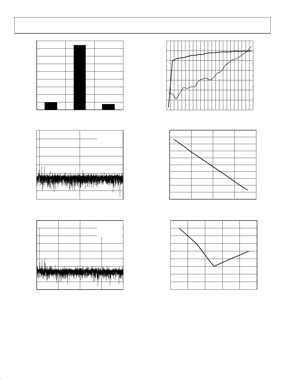
ADuC7019/20/21/22/24/25/26/27/28/29
–
9000
8000
7000
6000
5000
4000
FREQUENCY
3000
2000
1000
0
1161 1162 1163
BIN
Figure 24. Code Histogram Plot, fs = 774 kSPS, V
0
–20
–40
–60
–80
(dB)
–100
–120
–140
–160
0100
FREQUENCY (kHz)
Figure 25. Dynamic Performance, f
20
0
–20
–40
–60
(dB)
–80
–100
–120
–140
–160
0110050 200
FREQUENCY (kHz)
Figure 26. Dynamic Performance, f
f
= 774kSPS,
S
SNR = 69.3dB,
THD = –80.8dB,
PHSN = –83.4d B
= 774 kSPS
S
f
= 1MSPS,
S
SNR = 70.4dB,
THD = –77.2dB,
PHSN = –78.9d B
50
= 1 MSPS
S
= 0.7 V
IN
04955-073
04955-078
200
04955-079
75
70
65
60
55
SNR (dB)
50
45
40
1.0 1.5 2.0 2.5 3.0
SNR
THD
EXTERNAL REF ERENCE (V)
Figure 27. Typical Dynamic Performance vs. V
1500
1450
1400
1350
1300
1250
CODE
1200
1150
1100
1050
1000
–50 0 50 100
TEMPERATURE (°C)
76
–78
–80
–82
–84
–86
–88
REF
04955-060
150
Figure 28. On-Chip Temperature Sensor Voltage Output vs. Temperature
39.8
39.7
39.6
39.5
39.4
(mA)
39.3
39.2
39.1
39.0
38.9
–40 25 850 125
TEMPERATURE ( °C)
04955-080
Figure 29. Current Consumption vs. Temperature @ CD = 0
THD (dB)
04955-070
Rev. D | Page 32 of 96
Page 33

ADuC7019/20/21/22/24/25/26/27/28/29
12.05
12.00
11.95
11.90
11.85
11.80
(mA)
11.75
11.70
11.65
11.60
11.55
–40 25 850 125
TEMPERATURE ( °C)
04955-081
Figure 30. Current Consumption vs. Temperature @ CD = 3 Figure 32. Current Consumption vs. Temperature in Sleep Mode
7.85
7.80
7.75
7.70
7.65
(mA)
7.60
7.55
7.50
7.45
7.40
–40 25 850 125
TEMPERATURE ( °C)
04955-082
Figure 31. Current Consumption vs. Temperature @ CD = 7 Figure 33. Current Consumption vs. Sampling Frequency
1.4
1.2
1.0
0.8
(mA)
0.6
0.4
0.2
0
–40 25 850 125
37.4
37.2
37.0
36.8
(mA)
36.6
36.4
36.2
62.25 250.00 500.00125.00 1000.00
TEMPERATURE ( °C)
SAMPLING FREQUENCY (kSPS)
04955-083
04955-084
Rev. D | Page 33 of 96
Page 34

ADuC7019/20/21/22/24/25/26/27/28/29
TERMINOLOGY
ADC SPECIFICATIONS
Integral Nonlinearity (INL)
The maximum deviation of any code from a straight line
passing through the endpoints of the ADC transfer function.
The endpoints of the transfer function are zero scale, a point
½ LSB below the first code transition, and full scale, a point
½ LSB above the last code transition.
Differential Nonlinearity (DNL)
The difference between the measured and the ideal 1 LSB
change between any two adjacent codes in the ADC.
Offset Error
The deviation of the first code transition (0000 . . . 000) to
(0000 . . . 001) from the ideal, that is, +½ LSB.
Gain Error
The deviation of the last code transition from the ideal AIN
voltage (full scale − 1.5 LSB) after the offset error has been
adjusted out.
Signal to (Noise + Distortion) Ratio (SINAD)
The measured ratio of signal to (noise + distortion) at the
output of the ADC. The signal is the rms amplitude of the
fundamental. Noise is the rms sum of all nonfundamental
signals up to half the sampling frequency (f
/2), excluding dc.
S
The ratio is dependent upon the number of quantization levels
in the digitization process; the more levels, the smaller the
quantization noise.
The theoretical signal to (noise + distortion) ratio for an ideal
N-bit converter with a sine wave input is given by
Signal to (Noise + Distortion) = (6.02 N + 1.76) dB
Thus, for a 12-bit converter, this is 74 dB.
Total Harmonic Distortion (THD)
The ratio of the rms sum of the harmonics to the fundamental.
DAC SPECIFICATIONS
Relative Accuracy
Otherwise known as endpoint linearity, relative accuracy is a
measure of the maximum deviation from a straight line passing
through the endpoints of the DAC transfer function. It is
measured after adjusting for zero error and full-scale error.
Voltage Output Settling Time
The amount of time it takes the output to settle to within a
1 LSB level for a full-scale input change.
Rev. D | Page 34 of 96
Page 35

ADuC7019/20/21/22/24/25/26/27/28/29
OVERVIEW OF THE ARM7TDMI CORE
The ARM7® core is a 32-bit reduced instruction set computer
(RISC). It uses a single 32-bit bus for instruction and data. The
length of the data can be eight bits, 16 bits, or 32 bits. The
length of the instruction word is 32 bits.
The ARM7TDMI is an ARM7 core with four additional features.
• T support for the thumb (16-bit) instruction set.
• D support for debug.
• M support for long multiplications.
• I includes the EmbeddedICE module to support embedded
system debugging.
THUMB MODE (T)
An ARM instruction is 32 bits long. The ARM7TDMI processor
supports a second instruction set that is compressed into 16 bits,
called the thumb instruction set. Faster execution from 16-bit
memory and greater code density can usually be achieved by
using the thumb instruction set instead of the ARM instruction
set, which makes the ARM7TDMI core particularly suitable for
embedded applications.
However, the thumb mode has two limitations.
• Thumb code typically requires more instructions for the
same job. As a result, ARM code is usually best for
maximizing the performance of time-critical code.
• The thumb instruction set does not include some of the
instructions needed for exception handling, which
automatically switches the core to ARM code for exception
handling.
See the ARM7TDMI user guide for details on the core
architecture, the programming model, and both the ARM
and ARM thumb instruction sets.
LONG MULTIPLY (M)
The ARM7TDMI instruction set includes four extra instructions that perform 32-bit by 32-bit multiplication with a 64-bit
result, and 32-bit by 32-bit multiplication-accumulation (MAC)
with a 64-bit result. These results are achieved in fewer cycles
than required on a standard ARM7 core.
EmbeddedICE (I)
EmbeddedICE provides integrated on-chip support for the core.
The EmbeddedICE module contains the breakpoint and watchpoint registers that allow code to be halted for debugging purposes.
These registers are controlled through the JTAG test port.
When a breakpoint or watchpoint is encountered, the processor
halts and enters debug state. Once in a debug state, the
processor registers can be inspected as well as the Flash/EE,
SRAM, and memory mapped registers.
EXCEPTIONS
ARM supports five types of exceptions and a privileged
processing mode for each type. The five types of exceptions are
Rev. D | Page 35 of 96
• Normal interrupt or IRQ, which is provided to service
general-purpose interrupt handling of internal and
external events.
• Fast interrupt or FIQ, which is provided to service data
transfers or communication channels with low latency.
FIQ has priority over IRQ.
• Memory abort.
• Attempted execution of an undefined instruction.
• Software interrupt instruction (SWI), which can be used
to make a call to an operating system.
Typically, the programmer defines interrupt as IRQ, but for
higher priority interrupt, that is, faster response time, the
programmer can define interrupt as FIQ.
ARM REGISTERS
ARM7TDMI has a total of 37 registers: 31 general-purpose
registers and six status registers. Each operating mode has
dedicated banked registers.
When writing user-level programs, 15 general-purpose 32-bit
registers (R0 to R14), the program counter (R15), and the
current program status register (CPSR) are usable. The
remaining registers are used for system-level programming and
exception handling only.
When an exception occurs, some of the standard registers are
replaced with registers specific to the exception mode. All exception modes have replacement banked registers for the stack
pointer (R13) and the link register (R14), as represented in
Figure 34. The fast interrupt mode has more registers (R8 to R12)
for fast interrupt processing. This means that interrupt processing
can begin without the need to save or restore these registers
and, thus, save critical time in the interrupt handling process.
R13_ABT
R14_ABT
ABORT
MODE
USABLE IN USER M ODE
SYSTEM MODES ONLY
IRQ
R13_UND
R14_UND
SPSR_UND
UNDEFINED
MODE
R13_IRQ
R14_IRQ
SPSR_IRQ
MODE
R0
R1
R2
R3
R4
R5
R6
R7
R8
R9
R10
R11
R12
R13
R14
R15 (PC)
CPSR
USER MODE
R8_FIQ
R9_FIQ
R10_FIQ
R11_FIQ
R12_FIQ
R13_FIQ
R14_FIQ
SPSR_FIQ
R13_SVC
R14_SVC
SVC
MODE
SPSR_ABT
SPSR_SVC
FIQ
MODE
Figure 34. Register Organization
More information relative to the programmer’s model and the
ARM7TDMI core architecture can be found in the following
materials from ARM:
04955-007
Page 36

ADuC7019/20/21/22/24/25/26/27/28/29
• DDI0029G, ARM7TDMI Technical Reference Manual
• DDI-0100, ARM Architecture Reference Manual
INTERRUPT LATENCY
The worst-case latency for a fast interrupt request (FIQ)
consists of the following:
• The longest time the request can take to pass through the
synchronizer
• The time for the longest instruction to complete (the
longest instruction is an LDM) that loads all the registers
including the PC
• The time for the data abort entry
• The time for FIQ entry
At the end of this time, the ARM7TDMI executes the instruction at 0x1C (FIQ interrupt vector address). The maximum
total time is 50 processor cycles, which is just under 1.2 µs in a
system using a continuous 41.78 MHz processor clock.
The maximum interrupt request (IRQ) latency calculation is
similar but must allow for the fact that FIQ has higher priority
and may delay entry into the IRQ handling routine for an
arbitrary length of time. This time can be reduced to 42 cycles if
the LDM command is not used. Some compilers have an option
to compile without using this command. Another option is to run
the part in thumb mode where the time is reduced to 22 cycles.
The minimum latency for FIQ or IRQ interrupts is a total of
five cycles, which consist of the shortest time the request can
take through the synchronizer plus the time to enter the
exception mode.
Note that the ARM7TDMI always runs in ARM (32-bit) mode
when in privileged modes, for example, when executing
interrupt service routines.
Rev. D | Page 36 of 96
Page 37

ADuC7019/20/21/22/24/25/26/27/28/29
MEMORY ORGANIZATION
The ADuC7019/20/21/22/24/25/26/27/28/29 incorporate two
separate blocks of memory: 8 kB of SRAM and 64 kB of on-chip
Flash/EE memory. The 62 kB of on-chip Flash/EE memory is
available to the user, and the remaining 2 kB are reserved for
the factory-configured boot page. These two blocks are mapped
as shown in Figure 35.
0xFFFF 0000
0x40000000
0x30000000
0x20000000
0x10000000
0x00080000
0x00010000
0x00000000
0xFFFFFFFF
0x40000FFFF
0x30000FFFF
0x20000FFFF
0x10000FFFF
0x0008FFFF
0x00011FFF
0x0000FFFF
Figure 35. Physical Memory Map
MMRs
RESERVED
EXTERNAL ME MORY REGI ON 3
RESERVED
EXTERNAL ME MORY REGI ON 2
RESERVED
EXTERNAL ME MORY REGI ON 1
RESERVED
EXTERNAL ME MORY REGI ON 0
RESERVED
FLASH/EE
RESERVED
SRAM
REMAPPABLE MEMORY SPACE
(FLASH/EE OR SRAM)
04955-008
Note that by default, after a reset, the Flash/EE memory is
mirrored at Address 0x00000000. It is possible to remap the
SRAM at Address 0x00000000 by clearing Bit 0 of the REMAP
MMR. This remap function is described in more detail in the
Flash/EE Memory section.
MEMORY ACCESS
The ARM7 core sees memory as a linear array of a 232 byte
location where the different blocks of memory are mapped as
outlined in Figure 35.
The ADuC7019/20/21/22/24/25/26/27/28/29 memory organizations are configured in little endian format, which means that
the least significant byte is located in the lowest byte address,
and the most significant byte is in the highest byte address.
BIT 31
BYTE 3
.
.
.
B
7
3
BYTE 2
BYTE 1
.
.
.
.
.
.
A
9
6
5
2
1
32 BITS
Figure 36. Little Endian Format
BYTE 0
.
.
.
8
4
0
BIT 0
0xFFFFFFFF
0x00000004
0x00000000
4955-009
FLASH/EE MEMORY
The total 64 kB of Flash/EE memory is organized as 32 k × 16 bits;
31 k × 16 bits is user space and 1 k × 16 bits is reserved for the
on-chip kernel. The page size of this Flash/EE memory is 512 bytes.
Sixty-two kilobytes of Flash/EE memory are available to the
user as code and nonvolatile data memory. There is no
distinction between data and program because ARM code
shares the same space. The real width of the Flash/EE memory
is 16 bits, which means that in ARM mode (32-bit instruction),
two accesses to the Flash/EE are necessary for each instruction
fetch. It is therefore recommended to use thumb mode when
executing from Flash/EE memory for optimum access speed.
The maximum access speed for the Flash/EE memory is
41.78 MHz in thumb mode and 20.89 MHz in full ARM mode.
More details about Flash/EE access time are outlined in the
Execution Time from SRAM and Flash/EE section.
SRAM
Eight kilobytes of SRAM are available to the user, organized as
2 k × 32 bits, that is, two words. ARM code can run directly
from SRAM at 41.78 MHz, given that the SRAM array is
configured as a 32-bit wide memory array. More details about
SRAM access time are outlined in the Execution Time from
SRAM and Flash/EE section.
MEMORY MAPPED REGISTERS
The memory mapped register (MMR) space is mapped into the
upper two pages of the memory array and accessed by indirect
addressing through the ARM7 banked registers.
The MMR space provides an interface between the CPU and all
on-chip peripherals. All registers, except the core registers, reside
in the MMR area. All shaded locations shown in Figure 37 are
unoccupied or reserved locations and should not be accessed by
user software. Table 1 6 shows the full MMR memory map.
The access time for reading from or writing to an MMR
depends on the advanced microcontroller bus architecture
(AMBA) bus used to access the peripheral. The processor has
two AMBA buses: the advanced high performance bus (AHB)
used for system modules and the advanced peripheral bus
(APB) used for lower performance peripheral. Access to the
AHB is one cycle, and access to the APB is two cycles. All
peripherals on the ADuC7019/20/21/22/24/25/26/27/28/29 are
on the APB except the Flash/EE memory, the GPIOs (see
Tabl e 7 8 ), and the PWM.
Rev. D | Page 37 of 96
Page 38

ADuC7019/20/21/22/24/25/26/27/28/29
0xFFFFFFFF
0xFFFFFC3C
0xFFFFFC00
0xFFFFF820
0xFFFFF800
0xFFFFF46C
0xFFFFF400
0xFFFF0B54
0xFFFF0B00
0xFFFF0A14
0xFFFF0A00
0xFFFF0948
0xFFFF0900
0xFFFF0848
0xFFFF0800
0xFFFF0730
0xFFFF0700
0xFFFF0620
0xFFFF0600
0xFFFF0538
0xFFFF0500
0xFFFF0490
0xFFFF048C
0xFFFF0448
0xFFFF0440
0xFFFF0420
0xFFFF0404
0xFFFF0370
0xFFFF0360
0xFFFF0350
0xFFFF0340
0xFFFF0334
0xFFFF0320
0xFFFF0310
0xFFFF0300
0xFFFF0238
0xFFFF0220
0xFFFF0110
0xFFFF0000
PWM
FLASH CONTROL
INTERFACE
GPIO
PLA
SPI
I2C1
I2C0
UART
DAC
ADC
BAND GAP
REFERENCE
POWER SUPPLY
MONITOR
PLL AND
OSCILLATOR CONTROL
WATCHDOG
TIMER
WAKE-UP
TIMER
GENERAL-PURPOSE
TIMER
TIMER 0
REMAP AND
SYSTEM CONTROL
INTERRUPT
CONTROLLE R
Figure 37. Memory Mapped Registers
04955-010
Table 16. Complete MMR List
Address Name Byte
Access
Typ e
Default
Value Page
IRQ Address Base = 0xFFFF0000
0x0000 IRQSTA 4 R 0x00000000 78
0x0004 IRQSIG1 4 R 0x00XXX000 78
0x0008 IRQEN 4 R/W 0x00000000
0x000C IRQCLR 4 W 0x00000000
0x0010 SWICFG 4 W 0x00000000
0x0100 FIQSTA 4 R 0x00000000
0x0104 FIQSIG
1
4 R 0x00XXX000 79
0x0108 FIQEN 4 R/W 0x00000000
0x010C FIQCLR 4 W 0x00000000
1
Depends on the level on the external interrupt pins (P0.4, P0.5, P1.4, and P1.5).
78
78
79
79
79
79
System Control Address Base = 0xFFFF0200
0x0220 REMAP 1 R/W 0xXX
1
51
0x0230 RSTSTA 1 R/W 0x01 51
0x0234 RSTCLR 1 W 0x00
1
Depends on the model.
51
Timer Address Base = 0xFFFF0300
0x0300 T0LD 2 R/W 0x0000 80
0x0304 T0VAL 2 R 0xFFFF 80
0x0308 T0CON 2 R/W 0x0000
0x030C T0CLRI 1 W 0xFF
0x0320 T1LD 4 R/W 0x00000000
0x0324 T1VAL 4 R 0xFFFFFFFF
0x0328 T1CON 2 R/W 0x0000
0x032C T1CLRI 1 W 0xFF
0x0330 T1CAP 4 R/W 0x00000000
0x0340 T2LD 4 R/W 0x00000000
0x0344 T2VAL 4 R 0xFFFFFFFF
0x0348 T2CON 2 R/W 0x0000
0x034C T2CLRI 1 W 0xFF
0x0360 T3LD 2 R/W 0x0000
0x0364 T3VAL 2 R 0xFFFF
0x0368 T3CON 2 R/W 0x0000
0x036C T3CLRI 1 W 0x00
80
80
80
80
80
81
81
81
81
81
82
82
82
82
83
PLL Base Address = 0xFFFF0400
0x0404 POWKEY1 2 W 0x0000 56
0x0408 POWCON 2 R/W 0x0003 56
0x040C POWKEY2 2 W 0x0000
0x0410 PLLKEY1 2 W 0x0000
0x0414 PLLCON 1 R/W 0x21
0x0418 PLLKEY2 2 W 0x0000
56
56
56
56
PSM Address Base = 0xFFFF0440
0x0440 PSMCON 2 R/W 0x0008 53
0x0444 CMPCON 2 R/W 0x0000 54
Rev. D | Page 38 of 96
Page 39
ADuC7019/20/21/22/24/25/26/27/28/29
Access
Address Name Byte
Reference Address Base = 0xFFFF0480
0x048C REFCON 1 R/W 0x00 46
ADC Address Base = 0xFFFF0500
0x0500 ADCCON 2 R/W 0x0600 42
0x0504 ADCCP 1 R/W 0x00 43
0x0508 ADCCN 1 R/W 0x01 43
0x050C ADCSTA 1 R 0x00 44
0x0510 ADCDAT 4 R 0x00000000 44
0x0514 ADCRST 1 R/W 0x00 44
0x0530 ADCGN 2 R/W 0x0200 44
0x0534 ADCOF 2 R/W 0x0200 44
DAC Address Base = 0xFFFF0600
0x0600 DAC0CON 1 R/W 0x00 52
0x0604 DAC0DAT 4 R/W 0x00000000 52
0x0608 DAC1CON 1 R/W 0x00 52
0x060C DAC1DAT 4 R/W 0x00000000 52
0x0610 DAC2CON 1 R/W 0x00 52
0x0614 DAC2DAT 4 R/W 0x00000000 52
0x0618 DAC3CON 1 R/W 0x00 52
0x061C DAC3DAT 4 R/W 0x00000000 52
UART Base Address = 0xFFFF0700
0x0700 COMTX 1 R/W 0x00 66
COMRX 1 R 0x00 66
COMDIV0 1 R/W 0x00 66
0x0704 COMIEN0 1 R/W 0x00 66
COMDIV1 1 R/W 0x00 66
0x0708 COMIID0 1 R 0x01 67
0x070C COMCON0 1 R/W 0x00 67
0x0710 COMCON1 1 R/W 0x00 67
0x0714 COMSTA0 1 R 0x60 67
0x0718 COMSTA1 1 R 0x00 68
0x071C COMSCR 1 R/W 0x00 68
0x0720 COMIEN1 1 R/W 0x04 68
0x0724 COMIID1 1 R 0x01 68
0x0728 COMADR 1 R/W 0xAA 69
0x072C COMDIV2 2 R/W 0x0000 68
Typ e
Default
Value Page
Access
Address Name Byte
I2C0 Base Address = 0xFFFF0800
0x0800 I2C0MSTA 1 R/W 0x00 71
0x0804 I2C0SSTA 1 R 0x01 71
0x0808 I2C0SRX 1 R 0x00 72
0x080C I2C0STX 1 W 0x00 72
0x0810 I2C0MRX 1 R 0x00 72
0x0814 I2C0MTX 1 W 0x00 72
0x0818 I2C0CNT 1 R/W 0x00 72
0x081C I2C0ADR 1 R/W 0x00 72
0x0824 I2C0BYTE 1 R/W 0x00 72
0x0828 I2C0ALT 1 R/W 0x00 73
0x082C I2C0CFG 1 R/W 0x00 73
0x0830 I2C0DIV 2 R/W 0x1F1F 74
0x0838 I2C0ID0 1 R/W 0x00 74
0x083C I2C0ID1 1 R/W 0x00 74
0x0840 I2C0ID2 1 R/W 0x00 74
0x0844 I2C0ID3 1 R/W 0x00 74
0x0848 I2C0CCNT 1 R/W 0x01 74
0x084C I2C0FSTA 2 R/W 0x0000 74
I2C1 Base Address = 0xFFFF0900
0x0900 I2C1MSTA 1 R/W 0x00 71
0x0904 I2C1SSTA 1 R 0x01 71
0x0908 I2C1SRX 1 R 0x00 72
0x090C I2C1STX 1 W 0x00 72
0x0910 I2C1MRX 1 R 0x00 72
0x0914 I2C1MTX 1 W 0x00 72
0x0918 I2C1CNT 1 R/W 0x00 72
0x091C I2C1ADR 1 R/W 0x00 72
0x0924 I2C1BYTE 1 R/W 0x00 72
0x0928 I2C1ALT 1 R/W 0x00 73
0x092C I2C1CFG 1 R/W 0x00 73
0x0930 I2C1DIV 2 R/W 0x1F1F 74
0x0938 I2C1ID0 1 R/W 0x00 74
0x093C I2C1ID1 1 R/W 0x00 74
0x0940 I2C1ID2 1 R/W 0x00 74
0x0944 I2C1ID3 1 R/W 0x00 74
0x0948 I2C1CCNT 1 R/W 0x01 74
0x094C I2C1FSTA 2 R/W 0x0000 74
SPI Base Address = 0xFFFF0A00
0x0A00 SPISTA 1 R 0x00 70
0x0A04 SPIRX 1 R 0x00 70
0x0A08 SPITX 1 W 0x00 70
0x0A0C SPIDIV 1 R/W 0x1B 70
0x0A10 SPICON 2 R/W 0x0000 70
Typ e
Default
Value Page
Rev. D | Page 39 of 96
Page 40

ADuC7019/20/21/22/24/25/26/27/28/29
Access
Address Name Byte
Typ e
PLA Base Address = 0xFFFF0B00
0x0B00 PLAELM0 2 R/W 0x0000 75
0x0B04 PLAELM1 2 R/W 0x0000 75
0x0B08 PLAELM2 2 R/W 0x0000 75
0x0B0C PLAELM3 2 R/W 0x0000 75
0x0B10 PLAELM4 2 R/W 0x0000 75
0x0B14 PLAELM5 2 R/W 0x0000 75
0x0B18 PLAELM6 2 R/W 0x0000 75
0x0B1C PLAELM7 2 R/W 0x0000 75
0x0B20 PLAELM8 2 R/W 0x0000 75
0x0B24 PLAELM9 2 R/W 0x0000 75
0x0B28 PLAELM10 2 R/W 0x0000 75
0x0B2C PLAELM11 2 R/W 0x0000 75
0x0B30 PLAELM12 2 R/W 0x0000 75
0x0B34 PLAELM13 2 R/W 0x0000 75
0x0B38 PLAELM14 2 R/W 0x0000 75
0x0B3C PLAELM15 2 R/W 0x0000 75
0x0B40 PLACLK 1 R/W 0x00 76
0x0B44 PLAIRQ 4 R/W 0x00000000 76
0x0B48 PLAADC 4 R/W 0x00000000 77
0x0B4C PLADIN 4 R/W 0x00000000 77
0x0B50 PLADOUT 4 R 0x00000000 77
0x0B54 PLALCK 1 W 0x00 77
External Memory Base Address = 0xFFFFF000
0xF000 XMCFG 1 R/W 0x00 84
0xF010 XM0CON 1 R/W 0x00 84
0xF014 XM1CON 1 R/W 0x00 84
0xF018 XM2CON 1 R/W 0x00 84
0xF01C XM3CON 1 R/W 0x00 84
0xF020 XM0PAR 2 R/W 0x70FF 84
0xF024 XM1PAR 2 R/W 0x70FF 84
0xF028 XM2PAR 2 R/W 0x70FF 84
0xF02C XM3PAR 2 R/W 0x70FF 84
Default
Value Page
Address Name Byte
Access
Typ e
Default
Value Page
GPIO Base Address = 0xFFFFF400
0xF400 GP0CON 4 R/W 0x00000000 64
0xF404 GP1CON 4 R/W 0x00000000 64
0xF408 GP2CON 4 R/W 0x00000000 64
0xF40C GP3CON 4 R/W 0x00000000 64
0xF410 GP4CON 4 R/W 0x00000000 64
0xF420 GP0DAT 4 R/W 0x000000XX1 65
0xF424 GP0SET 4 W 0x000000XX1 65
0xF428 GP0CLR 4 W 0x000000XX1 65
0xF42C GP0PAR 4 R/W 0x20000000 64
0xF430 GP1DAT 4 R/W 0x000000XX1 65
0xF434 GP1SET 4 W 0x000000XX1 65
0xF438 GP1CLR 4 W 0x000000XX1 65
0xF43C GP1PAR 4 R/W 0x00000000 64
0xF440 GP2DAT 4 R/W 0x000000XX1 65
0xF444 GP2SET 4 W 0x000000XX1 65
0xF448 GP2CLR 4 W 0x000000XX1 65
0xF450 GP3DAT 4 R/W 0x000000XX1 65
0xF454 GP3SET 4 W 0x000000XX1 65
0xF458 GP3CLR 4 W 0x000000XX1 65
0xF460 GP4DAT 4 R/W 0x000000XX1 65
0xF464 GP4SET 4 W 0x000000XX1 65
0xF468 GP4CLR 4 W 0x000000XX1 65
1
X = 0, 1, 2, or 3.
Flash/EE Base Address = 0xFFFFF800
0xF800 FEESTA 1 R 0x20 48
0xF804 FEEMOD 2 R/W 0x0000 48
0xF808 FEECON 1 R/W 0x07 49
0xF80C FEEDAT 2 R/W 0xXXXX1 49
0xF810 FEEADR 2 R/W 0x0000 49
0xF818 FEESIGN 3 R 0xFFFFFF 49
0xF81C FEEPRO 4 R/W 0x00000000 49
0xF820 FEEHIDE 4 R/W 0xFFFFFFFF 49
1
X = 0, 1, 2, or 3.
PWM Base Address = 0xFFFFFC00
0xFC00 PWMCON 2 R/W 0x0000 62
0xFC04 PWMSTA 2 R/W 0x0000 62
0xFC08 PWMDAT0 2 R/W 0x0000 63
0xFC0C PWMDAT1 2 R/W 0x0000 63
0xFC10 PWMCFG 2 R/W 0x0000 63
0xFC14 PWMCH0 2 R/W 0x0000 63
0xFC18 PWMCH1 2 R/W 0x0000 63
0xFC1C PWMCH2 2 R/W 0x0000 63
0xFC20 PWMEN 2 R/W 0x0000 63
0xFC24 PWMDAT2 2 R/W 0x0000 63
Rev. D | Page 40 of 96
Page 41
ADuC7019/20/21/22/24/25/26/27/28/29
ADC CIRCUIT OVERVIEW
The analog-to-digital converter (ADC) incorporates a fast,
multichannel, 12-bit ADC. It can operate from 2.7 V to 3.6 V
supplies and is capable of providing a throughput of up to
1 MSPS when the clock source is 41.78 MHz. This block
provides the user with a multichannel multiplexer, a differential
track-and-hold, an on-chip reference, and an ADC.
The ADC consists of a 12-bit successive approximation converter
based around two capacitor DACs. Depending on the input
signal configuration, the ADC can operate in one of three modes.
• Fully differential mode, for small and balanced signals
• Single-ended mode, for any single-ended signals
• Pseudo differential mode, for any single-ended signals,
taking advantage of the common-mode rejection offered
by the pseudo differential input
The converter accepts an analog input range of 0 V to V
REF
when
operating in single-ended or pseudo differential mode. In fully
differential mode, the input signal must be balanced around a
common-mode voltage (V
maximum amplitude of 2 V
AV
DD
V
CM
0
Figure 38. Examples of Balanced Signals in Fully Differential Mode
) in the 0 V to AVDD range with a
CM
(see Figure 38).
REF
V
CM
2V
REF
V
CM
2V
REF
2V
REF
04955-011
A high precision, low drift, factory calibrated, 2.5 V reference is
provided on-chip. An external reference can also be connected as
described in the Band Gap Reference section.
Single or continuous conversion modes can be initiated in the
CONV
software. An external
START
pin, an output generated from
the on-chip PLA, or a Timer0 or Timer1 overflow can also be
used to generate a repetitive trigger for ADC conversions.
A voltage output from an on-chip band gap reference proportional to absolute temperature can also be routed through the
front-end ADC multiplexer, effectively an additional ADC channel
input. This facilitates an internal temperature sensor channel
that measures die temperature to an accuracy of ±3°C.
TRANSFER FUNCTION
Pseudo Differential and Single-Ended Modes
In pseudo differential or single-ended mode, the input range is
0 V to V
differential and single-ended modes with
. The output coding is straight binary in pseudo
REF
1 LSB = FS/4096, or
2.5 V/4096 = 0.61 mV, or
610 µV when V
= 2.5 V
REF
The ideal code transitions occur midway between successive
integer LSB values (that is, 1/2 LSB, 3/2 LSB, 5/2 LSB, … ,
FS − 3/2 LSB). The ideal input/output transfer characteristic
is shown in Figure 39.
1111 1111 1111
1111 1111 1110
1111 1111 1101
1111 1111 1100
OUTPUT CODE
0000 0000 0011
0000 0000 0010
0000 0000 0001
0000 0000 0000
1LSB0V +FS – 1LSB
1LSB =
FS
4096
VOLTAGE INPUT
04955-012
Figure 39. ADC Transfer Function in Pseudo Differential or Single-Ended Mode
Fully Differential Mode
The amplitude of the differential signal is the difference between
the signals applied to the V
is, V
− V
IN+
signal is, therefore, –V
). The maximum amplitude of the differential
IN–
REF
IN+
to +V
and V
input voltage pins (that
IN–
p-p (that is, 2 × V
REF
). This is
REF
regardless of the common mode (CM). The common mode is
the average of the two signals, for example, (V
IN+
+ V
)/2, and
IN–
is, therefore, the voltage that the two inputs are centered on.
This results in the span of each input being CM ± V
voltage has to be set up externally, and its range varies with V
/2. This
REF
REF
(see the Driving the Analog Inputs section).
The output coding is twos complement in fully differential mode
with 1 LSB = 2 V
V
= 2.5 V. The output result is ±11 bits, but this is shifted by 1
REF
/4096 or 2 × 2.5 V/4096 = 1.22 mV when
REF
to the right. This allows the result in ADCDAT to be declared as a
signed integer when writing C code. The designed code
transitions occur midway between successive integer LSB values
(that is, 1/2 LSB, 3/2 LSB, 5/2 LSB, … , FS − 3/2 LSB). The ideal
input/output transfer characteristic is shown in Figure 40.
SIGN
BIT
0 1111 1111 1110
0 1111 1111 1100
0 1111 1111 1010
0 0000 0000 0010
0 0000 0000 0000
1 1111 1111 1110
OUTPUT CODE
1 0000 0000 0100
1 0000 0000 0010
1 0000 0000 0000
–V
Figure 40. ADC Transfer Function in Differential Mode
2 × V
1LSB =
+ 1LSB +V
REF
REF
4096
VOLTAGE INPUT (VIN+ – VIN–)
REF
– 1LSB0LSB
04955-013
Rev. D | Page 41 of 96
Page 42

ADuC7019/20/21/22/24/25/26/27/28/29
A
A
TYPICAL OPERATION
Once configured via the ADC control and channel selection
registers, the ADC converts the analog input and provides a
12-bit result in the ADC data register.
The top four bits are the sign bits. The 12-bit result is placed
from Bit 16 to Bit 27, as shown in Figure 41. Again, it should be
noted that, in fully differential mode, the result is represented in
twos complement format. In pseudo differential and singleended modes, the result is represented in straight binary format.
31 27 16 15 0
SIGN BITS 12-BIT ADC RESULT
Figure 41. ADC Result Format
The same format is used in DACxDAT, simplifying the software.
Current Consumption
The ADC in standby mode, that is, powered up but not
converting, typically consumes 640 µA. The internal reference
adds 140 µA. During conversion, the extra current is 0.3 µA
multiplied by the sampling frequency (in kilohertz (kHz)).
Figure 33 shows the current consumption vs. the sampling
frequency of the ADC.
Timing
Figure 42 gives details of the ADC timing. Users control the
ADC clock speed and the number of acquisition clocks in the
ADCCON MMR. By default, the acquisition time is eight clocks
and the clock divider is 2. The number of extra clocks (such as
bit trial or write) is set to 19, which gives a sampling rate of 774
kSPS. For conversion on the temperature sensor, the ADC
acquisition time is automatically set to 16 clocks, and the ADC
clock divider is set to 32. When using multiple channels,
including the temperature sensor, the timing settings revert to
the user-defined settings after reading the temperature sensor
channel.
CQ BIT TRIAL
ADC CLOCK
CONV
START
ADC
BUSY
ADCDAT
ADCSTA = 0 ADCSTA = 1
04955-014
Figure 42. ADC Timing
WRITE
DATA
ADC INTERRUPT
4955-015
ADuC7019
The ADuC7019 is identical to the ADuC7020 except for one
buffered ADC channel, ADC3, and it has only three DACs. The
output buffer of the fourth DAC is internally connected to the
ADC3 channel as shown in Figure 43.
ADuC7019
DC3
MUX
1MSPS
12-BIT ADC
ADC15
Figure 43. ADC3 Buffered Input
12-BIT
DAC
DAC3
04955-016
Note that the DAC3 output pin must be connected to a 10 nF
capacitor to AGND. This channel should be used to measure dc
voltages only. ADC calibration may be necessary on this channel.
MMRS INTERFACE
The ADC is controlled and configured via the eight MMRs
described in this section.
Table 17. ADCCON Register
Name Address Default Value Access
ADCCON 0xFFFF0500 0x0600 R/W
ADCCON is an ADC control register that allows the programmer
to enable the ADC peripheral, select the mode of operation of
the ADC (in single-ended mode, pseudo differential mode, or
fully differential mode), and select the conversion type. This
MMR is described in Ta b le 1 8.
Rev. D | Page 42 of 96
Page 43

ADuC7019/20/21/22/24/25/26/27/28/29
Table 18. ADCCON MMR Bit Designations
Bit Value Description
15:13 Reserved.
12:10 ADC clock speed.
000
fADC/1. This divider is provided to obtain
1 MSPS ADC with an external clock <41.78 MHz.
001 fADC/2 (default value).
010 fADC/4.
011 fADC/8.
100 fADC/16.
101 fADC/32.
9:8 ADC acquisition time.
00 Two clocks.
01 Four clocks.
10 Eight clocks (default value).
11 16 clocks.
7 Enable start conversion.
Set by the user to start any type of conversion
command. Cleared by the user to disable a
start conversion (clearing this bit does not
stop the ADC when continuously converting).
6 Enable ADC
Set by the user to enable the ADC
BUSY
.
Cleared by the user to disable the ADC
5 ADC power control.
Set by the user to place the ADC in normal
mode (the ADC must be powered up for at least
5 s before it converts correctly). Cleared by the
user to place the ADC in power-down mode.
4:3 Conversion mode.
00 Single-ended mode.
01 Differential mode.
10 Pseudo differential mode.
11 Reserved.
2:0 Conversion type.
000
Enable CONV
pin as a conversion input.
START
001 Enable Timer1 as a conversion input.
010 Enable Timer0 as a conversion input.
011
Single software conversion. Sets to 000 after
conversion (note that Bit 7 of ADCCON MMR
should be cleared after starting a single
software conversion to avoid further
conversions triggered by the CONV
100 Continuous software conversion.
101 PLA conversion.
Other Reserved.
BUSY
START
pin.
BUSY
pin).
pin.
Table 19. ADCCP Register
Name Address Default Value Access
ADCCP 0xFFFF0504 0x00 R/W
ADCCP is an ADC positive channel selection register. This
MMR is described in Ta b le 2 0.
Table 20. ADCCP
1
MMR Bit Designation
Bit Value Description
7:5 Reserved.
4:0 Positive channel selection bits.
00000 ADC0.
00001 ADC1.
00010 ADC2.
00011 ADC3.
00100 ADC4.
00101 ADC5.
00110 ADC6.
00111 ADC7.
01000 ADC8.
01001 ADC9.
01010 ADC10.
01011 ADC11.
01100 DAC0/ADC12.
01101 DAC1/ADC13.
01110 DAC2/ADC14.
01111 DAC3/ADC15.
10000 Temperature sensor.
10001 AGND (self-diagnostic feature).
10010 Internal reference (self-diagnostic feature).
10011 AVDD/2.
Others Reserved.
1
ADC and DAC channel availability depends on the part model. See Ordering
Guide for details.
Table 21. ADCCN Register
Name Address Default Value Access
ADCCN 0xFFFF0508 0x01 R/W
ADCCN is an ADC negative channel selection register. This
MMR is described in Ta b le 2 2.
Rev. D | Page 43 of 96
Page 44

ADuC7019/20/21/22/24/25/26/27/28/29
Table 22. ADCCN MMR Bit Designation
Bit Value
7:5 Reserved.
4:0 Negative channel selection bits.
00000 ADC0.
00001 ADC1.
00010 ADC2.
00011
00100
00101
00110
00111 ADC7.
01000 ADC8.
01001
01010
01011
01100
01101
01110
01111
10000
Others Reserved.
Table 23. ADCSTA Register
Name Address Default Value Access
ADCSTA 0xFFFF050C 0x00 R
ADCSTA is an ADC status register that indicates when an ADC
conversion result is ready. The ADCSTA register contains only
one bit, ADCReady (Bit 0), representing the status of the ADC.
This bit is set at the end of an ADC conversion, generating an
ADC interrupt. It is cleared automatically by reading the
ADCDAT MMR. When the ADC is performing a conversion,
the status of the ADC can be read externally via the ADC
pin. This pin is high during a conversion. When the conversion
is finished, ADC
available on P0.5 (see the General-Purpose Input/Output
section) if enabled in the ADCCON register.
Table 24. ADCDAT Register
Name Address Default Value Access
ADCDAT 0xFFFF0510 0x00000000 R
ADCDAT is an ADC data result register. It holds the 12-bit
ADC result as shown in Figure 41.
Table 25. ADCRST Register
Name Address Default Value Access
ADCRST 0xFFFF0514 0x00 R/W
ADCRST resets the digital interface of the ADC. Writing any value
to this register resets all the ADC registers to their default values.
Table 26. ADCGN Register
Name Address Default Value Access
ADCGN 0xFFFF0530 0x0200 R/W
ADCGN is a 10-bit gain calibration register.
Description
ADC3.
ADC4.
ADC5.
ADC6.
ADC9.
ADC10.
ADC11.
DAC0/ADC12.
DAC1/ADC13.
DAC2/ADC14.
DAC3/ADC15.
Internal reference (self-diagnostic feature).
goes back low. This information can be
BUSY
BUSY
Table 27. ADCOF Register
Name Address Default Value
Access
ADCOF 0xFFFF0534 0x0200 R/W
ADCOF is a 10-bit offset calibration register.
CONVERTER OPERATION
The ADC incorporates a successive approximation (SAR)
architecture involving a charge-sampled input stage. This
architecture can operate in three modes: differential, pseudo
differential, and single-ended.
Differential Mode
The ADuC7019/20/21/22/24/25/26/27/28/29 each contain a
successive approximation ADC based on two capacitive DACs.
Figure 44 and Figure 45 show simplified schematics of the ADC
in acquisition and conversion phase, respectively. The ADC
comprises control logic, a SAR, and two capacitive DACs. In
Figure 44 (the acquisition phase), SW3 is closed and SW1 and
SW2 are in Position A. The comparator is held in a balanced
condition, and the sampling capacitor arrays acquire the
differential signal on the input.
CAPACITIVE
DAC
AIN0
AIN11
MUX
CHANNEL+
CHANNEL–
B
A
A
B
S
SW1
C
S
SW2
V
REF
C
Figure 44. ADC Acquisition Phase
When the ADC starts a conversion, as shown in Figure 45, SW3
opens, and then SW1 and SW2 move to Position B. This causes
the comparator to become unbalanced. Both inputs are disconnected once the conversion begins. The control logic and the
charge redistribution DACs are used to add and subtract fixed
amounts of charge from the sampling capacitor arrays to bring
the comparator back into a balanced condition. When the
comparator is rebalanced, the conversion is complete. The
control logic generates the ADC output code. The output
impedances of the sources driving the V
voltage pins must be matched; otherwise, the two inputs have
different settling times, resulting in errors.
C
AIN0
AIN11
MUX
CHANNEL+
CHANNEL–
B
A
A
B
Figure 45. ADC Conversion Phase
S
SW1
C
S
SW2
V
REF
COMPARAT OR
SW3
and V
IN+
COMPARATOR
SW3
CAPACITIVE
input
IN–
CAPACITIVE
CAPACITIVE
CONTROL
LOGIC
DAC
DAC
CONTROL
LOGIC
DAC
04955-017
04955-018
Rev. D | Page 44 of 96
Page 45

ADuC7019/20/21/22/24/25/26/27/28/29
A
V
Pseudo Differential Mode
In pseudo differential mode, Channel− is linked to the V
IN−
pin
of the ADuC7019/20/21/22/24/25/26/27/28/29. SW2 switches
between A (Channel−) and B (V
connected to ground or a low voltage. The input signal on V
can then vary from V
chosen so that V
AIN0
AIN11
V
IN–
CHANNEL+
MUX
CHANNEL–
Figure 46. ADC in Pseudo Differential Mode
REF
to V
IN−
+ V
does not exceed AVDD.
IN−
B
A
SW1
SW2
A
B
V
REF
C
C
REF
S
S
REF
+ V
). The V
IN−
pin must be
IN−
. Note that V
COMPARATOR
SW3
must be
IN−
CAPACITIVE
DAC
CONTROL
LOGIC
CAPACITIVE
DAC
IN+
Single-Ended Mode
In single-ended mode, SW2 is always connected internally to
ground. The V
V
is 0 V to V
IN+
AIN0
MUX
AIN11
pin can be floating. The input signal range on
IN−
.
REF
CHANNEL+
CHANNEL–
C
B
A
SW1
S
C
S
COMPARATOR
SW3
Figure 47. ADC in Single-Ended Mode
CAPACITIVE
DAC
CONTROL
LOGIC
CAPACITIVE
DAC
Analog Input Structure
Figure 48 shows the equivalent circuit of the analog input structure
of the ADC. The four diodes provide ESD protection for the analog
inputs. Care must be taken to ensure that the analog input
signals never exceed the supply rails by more than 300 mV;
exceeding 300 mV causes these diodes to become forwardbiased and start conducting into the substrate. These diodes can
conduct up to 10 mA without causing irreversible damage to
the part.
The C1 capacitors in Figure 48 are typically 4 pF and can be
primarily attributed to pin capacitance. The resistors are
lumped components made up of the on resistance of the
switches. The value of these resistors is typically about 100 Ω.
The C2 capacitors are the ADC’s sampling capacitors and
typically have a capacitance of 16 pF.
DD
D
C1
C1
D
AV
DD
D
D
C2
R1
C2
R1
04955-021
Figure 48. Equivalent Analog Input Circuit Conversion Phase: Switches Open,
Track Phase: Switches Closed
For ac applications, removing high frequency components from
04955-019
the analog input signal is recommended by using an RC lowpass filter on the relevant analog input pins. In applications
where harmonic distortion and signal-to-noise ratio are critical,
the analog input should be driven from a low impedance
source. Large source impedances significantly affect the ac
performance of the ADC. This can necessitate the use of an
input buffer amplifier. The choice of the op amp is a function of
the particular application. Figure 49 and Figure 50 give an
example of an ADC front end.
ADuC7019/
10Ω
0.01µF
04955-020
Figure 49. Buffering Single-Ended/Pseudo Differential Input
V
REF
Figure 50. Buffering Differential Inputs
ADuC702x
ADC0
ADuC7019/
ADuC702x
ADC0
ADC1
04955-061
04955-062
When no amplifier is used to drive the analog input, the source
impedance should be limited to values lower than 1 kΩ. The
maximum source impedance depends on the amount of total
harmonic distortion (THD) that can be tolerated. The THD
increases as the source impedance increases and the performance
degrades.
DRIVING THE ANALOG INPUTS
Internal or external references can be used for the ADC. In
the differential mode of operation, there are restrictions on the
common-mode input signal (V
the reference value and supply voltage used to ensure that the
signal remains within the supply rails. Tab l e 28 gives some
calculated V
minimum and VCM maximum values.
CM
), which is dependent upon
CM
Rev. D | Page 45 of 96
Page 46

ADuC7019/20/21/22/24/25/26/27/28/29
Table 28. VCM Ranges
AVDD V
3.3 V
3.0 V
VCM Min VCM Max Signal Peak-to-Peak
REF
2.5 V 1.25 V 2.05 V 2.5 V
2.048 V 1.024 V 2.276 V 2.048 V
1.25 V 0.75 V 2.55 V 1.25 V
2.5 V 1.25 V 1.75 V 2.5 V
2.048 V 1.024 V 1.976 V 2.048 V
1.25 V 0.75 V 2.25 V 1.25 V
CALIBRATION
By default, the factory-set values written to the ADC offset
(ADCOF) and gain coefficient registers (ADCGN) yield
optimum performance in terms of end-point errors and
linearity for standalone operation of the part (see the
Specifications section). If system calibration is required, it is
possible to modify the default offset and gain coefficients to
improve end-point errors, but note that any modification to the
factory-set ADCOF and ADCGN values can degrade ADC
linearity performance.
For system offset error correction, the ADC channel input stage
must be tied to AGND. A continuous software ADC conversion
loop must be implemented by modifying the value in ADCOF until
the ADC result (ADCDAT) reads Code 0 to Code 1. If the
ADCDAT value is greater than 1, ADCOF should be decremented
until ADCDAT reads 0 to 1. Offset error correction is done
digitally and has a resolution of 0.25 LSB and a range of
±3.125% of V
REF
.
For system gain error correction, the ADC channel input stage
must be tied to V
. A continuous software ADC conversion
REF
loop must be implemented to modify the value in ADCGN
until the ADC result (ADCDAT) reads Code 4094 to Code 4095.
If the ADCDAT value is less than 4094, ADCGN should be
incremented until ADCDAT reads 4094 to 4095. Similar to the
offset calibration, the gain calibration resolution is 0.25 LSB
with a range of ±3% of V
REF
.
TEMPERATURE SENSOR
The ADuC7019/20/21/22/24/25/26/27/28/29 provide voltage
output from on-chip band gap references proportional to
absolute temperature. This voltage output can also be routed
through the front-end ADC multiplexer (effectively an additional
ADC channel input) facilitating an internal temperature sensor
channel, measuring die temperature to an accuracy of ±3°C.
The following is an example routine showing how to use the
internal temperature sensor:
int main(void)
{
float a = 0;
short b;
ADCCON = 0x20; // power-on the ADC
delay(2000);
ADCCP = 0x10; // Select Temperature
Sensor as an // input to the ADC
REFCON = 0x01; // connect internal 2.5V
reference // to Vref pin
ADCCON = 0xE4; // continuous conversion
while(1)
{
while (!ADCSTA){};
// wait for end of conversion
b = (ADCDAT >> 16);
// To calculate temperature in °C, use
the formula:
a = 0x525 - b;
// ((Temperature = 0x525 - Sensor
Voltage) / 1.3)
a /= 1.3;
b = floor(a);
printf("Temperature: %d
oC\n",b);
}
return 0;
}
BAND GAP REFERENCE
Each ADuC7019/20/21/22/24/25/26/27/28/29 provides an onchip band gap reference of 2.5 V, which can be used for the ADC
and DAC. This internal reference also appears on the V
When using the internal reference, a 0.47 µF capacitor must be
connected from the external V
pin to AGND to ensure stability
REF
and fast response during ADC conversions. This reference can
also be connected to an external pin (V
) and used as a refer-
REF
ence for other circuits in the system. An external buffer is required
because of the low drive capability of the V
output. A program-
REF
mable option also allows an external reference input on the V
pin. Note that it is not possible to disable the internal reference.
Therefore, the external reference source must be capable of
overdriving the internal reference source.
Table 29. REFCON Register
Name Address Default Value Access
REFCON 0xFFFF048C 0x00 R/W
The band gap reference interface consists of an 8-bit MMR
REFCON, described in Ta ble 3 0.
Table 30. REFCON MMR Bit Designations
Bit Description
7:1 Reserved.
0
Internal reference output enable. Set by user to
connect the internal 2.5 V reference to the V
The reference can be used for an external component
but must be buffered. Cleared by user to disconnect
the reference from the V
REF
pin.
REF
REF
pin.
pin.
REF
Rev. D | Page 46 of 96
Page 47

ADuC7019/20/21/22/24/25/26/27/28/29
NONVOLATILE FLASH/EE MEMORY
The ADuC7019/20/21/22/24/25/26/27/28/29 incorporate
Flash/EE memory technology on-chip to provide the user with
nonvolatile, in-circuit reprogrammable memory space.
Like EEPROM, flash memory can be programmed in-system
at a byte level, although it must first be erased. The erase is
performed in page blocks. As a result, flash memory is often
and more correctly referred to as Flash/EE memory.
Overall, Flash/EE memory represents a step closer to the
ideal memory device that includes nonvolatility, in-circuit
programmability, high density, and low cost. Incorporated in
the ADuC7019/20/21/22/24/25/26/27/28/29, Flash/EE memory
technology allows the user to update program code space incircuit, without the need to replace one-time programmable
(OTP) devices at remote operating nodes.
Each part contains a 64 kB array of Flash/EE memory. The
lower 62 kB is available to the user and the upper 2 kB contain
permanently embedded firmware, allowing in-circuit serial
download. These 2 kB of embedded firmware also contain a
power-on configuration routine that downloads factorycalibrated coefficients to the various calibrated peripherals
(such as ADC, temperature sensor, and band gap references).
This 2 kB embedded firmware is hidden from user code.
Flash/EE Memory Reliability
The Flash/EE memory arrays on the parts are fully qualified for
two key Flash/EE memory characteristics: Flash/EE memory
cycling endurance and Flash/EE memory data retention.
Endurance quantifies the ability of the Flash/EE memory to be
cycled through many program, read, and erase cycles. A single
endurance cycle is composed of four independent, sequential
events, defined as
1. Initial page erase sequence
2. Read/verify sequence (single Flash/EE)
3. Byte program sequence memory
4. Second read/verify sequence (endurance cycle)
In reliability qualification, every half word (16-bit wide)
location of the three pages (top, middle, and bottom) in the
Flash/EE memory is cycled 10,000 times from 0x0000 to
0xFFFF. As indicated in Tab le 1 , the Flash/EE memory
endurance qualification is carried out in accordance with
JEDEC Retention Lifetime Specification A117 over the
industrial temperature range of −40° to +125°C. The results
allow the specification of a minimum endurance figure over a
supply temperature of 10,000 cycles.
Retention quantifies the ability of the Flash/EE memory to
retain its programmed data over time. Again, the parts are
qualified in accordance with the formal JEDEC Retention
Lifetime Specification (A117) at a specific junction temperature
(T
= 85°C). As part of this qualification procedure, the
J
Flash/EE memory is cycled to its specified endurance limit,
described in Ta bl e 1, before data retention is characterized. This
means that the Flash/EE memory is guaranteed to retain its data
for its fully specified retention lifetime every time the Flash/EE
memory is reprogrammed. In addition, note that retention
lifetime, based on an activation energy of 0.6 eV, derates with T
as shown in Figure 51.
600
450
300
RETENTION (Years)
150
0
30 40 55 70 85 100 125 135 150
JUNCTION TEM PERATURE (°C)
Figure 51. Flash/EE Memory Data Retention
04955-085
PROGRAMMING
The 62 kB of Flash/EE memory can be programmed in-circuit,
using the serial download mode or the provided JTAG mode.
Serial Downloading (In-Circuit Programming)
The ADuC7019/20/21/22/24/25/26/27/28/29 facilitate code
download via the standard UART serial port or via the I
The parts enter serial download mode after a reset or power
cycle if the BM pin is pulled low through an external 1 kΩ
resistor. After a part is in serial download mode, the user can
download code to the full 62 kB of Flash/EE memory while the
device is in-circuit in its target application hardware. An
executable PC serial download is provided as part of the
development system for serial downloading via the UART. The
AN-806 Application Note
downloading via the UART and I
describes the protocol for serial
2
C.
JTAG Access
The JTAG protocol uses the on-chip JTAG interface to facilitate
code download and debug.
2
C port.
J
Rev. D | Page 47 of 96
Page 48
ADuC7019/20/21/22/24/25/26/27/28/29
SECURITY
The 62 kB of Flash/EE memory available to the user can be read
and write protected.
Bit 31 of the FEEPRO/FEEHIDE MMR (see Tab le 4 2) protects
the 62 kB from being read through JTAG programming mode.
The other 31 bits of this register protect writing to the flash
memory. Each bit protects four pages, that is, 2 kB. Write
protection is activated for all types of access.
Three Levels of Protection
• Protection can be set and removed by writing directly into
FEEHIDE MMR. This protection does not remain after reset.
• Protection can be set by writing into the FEEPRO MMR. It
takes effect only after a save protection command (0x0C)
and a reset. The FEEPRO MMR is protected by a key to
avoid direct access. The key is saved once and must be
entered again to modify FEEPRO. A mass erase sets the
key back to 0xFFFF but also erases all the user code.
• Flash can be permanently protected by using the FEEPRO
MMR and a particular value of key: 0xDEADDEAD.
Entering the key again to modify the FEEPRO register is
not allowed.
Sequence to Write the Key
1. Write the bit in FEEPRO corresponding to the page to be
protected.
2. Enable key protection by setting Bit 6 of FEEMOD (Bit 5
must equal 0).
3. Write a 32-bit key in FEEADR and FEEDAT.
4. Run the write key command 0x0C in FEECON; wait for
the read to be successful by monitoring FEESTA.
5. Reset the part.
To remove or modify the protection, the same sequence is used
with a modified value of FEEPRO. If the key chosen is the value
0xDEAD, the memory protection cannot be removed. Only a mass
erase unprotects the part, but it also erases all user code.
The sequence to write the key is illustrated in the following
example (this protects writing Page 4 to Page 7 of the Flash):
FEEPRO=0xFFFFFFFD; //Protect pages 4 to 7
FEEMOD=0x48; //Write key enable
FEEADR=0x1234; //16 bit key value
FEEDAT=0x5678; //16 bit key value
FEECON= 0x0C; // Write key command
The same sequence should be followed to protect the part
permanently with FEEADR = 0xDEAD and FEEDAT = 0xDEAD.
FLASH/EE CONTROL INTERFACE
Serial and JTAG programming use the Flash/EE control interface,
which includes the eight MMRs outlined in this section.
Table 31. FEESTA Register
Name Address Default Value Access
FEESTA 0xFFFFF800 0x20 R
FEESTA is a read-only register that reflects the status of the
flash control interface as described in Tab l e 3 2 .
Table 32. FEESTA MMR Bit Designations
Bit Description
15:6 Reserved.
5 Reserved.
4 Reserved.
3
2
1
0
Table 33. FEEMOD Register
Name Address Default Value Access
FEEMOD 0xFFFFF804 0x0000 R/W
FEEMOD sets the operating mode of the flash control interface.
Tabl e 3 4 shows FEEMOD MMR bit designations.
Table 34. FEEMOD MMR Bit Designations
Bit Description
15:9 Reserved.
8 Reserved. This bit should always be set to 0.
7:5
4
3
2:0 Reserved. These bits should always be set to 0.
Flash interrupt status bit. Set automatically when an
interrupt occurs, that is, when a command is complete
and the Flash/EE interrupt enable bit in the FEEMOD
register is set. Cleared when reading the FEESTA register.
Flash/EE controller busy. Set automatically when the
controller is busy. Cleared automatically when the
controller is not busy.
Command fail. Set automatically when a command
completes unsuccessfully. Cleared automatically when
reading the FEESTA register.
Command pass. Set by the MicroConverter when a
command completes successfully. Cleared automatically when reading the FEESTA register.
Reserved. These bits should always be set to 0 except
when writing keys. See the Sequence to Write the Key
section.
Flash/EE interrupt enable. Set by user to enable the
Flash/EE interrupt. The interrupt occurs when a
command is complete. Cleared by user to disable
the Flash/EE interrupt.
Erase/write command protection. Set by user to
enable the erase and write commands. Cleared to
protect the Flash against the erase/write command.
Rev. D | Page 48 of 96
Page 49

ADuC7019/20/21/22/24/25/26/27/28/29
Table 35. FEECON Register
Name Address Default Value Access
FEECON 0xFFFFF808 0x07 R/W
FEECON is an 8-bit command register. The commands are
described in Ta bl e 36 .
Table 37. FEEDAT Register
Name Address Default Value Access
FEEDAT 0xFFFFF80C 0xXXXX1 R/W
1
X = 0, 1, 2, or 3.
FEEDAT is a 16-bit data register.
Table 36. Command Codes in FEECON
Code Command Description
0x001 Null Idle state.
0x011 Single read
Load FEEDAT with the 16-bit data.
Indexed by FEEADR.
0x021 Single write
Write FEEDAT at the address pointed to
by FEEADR. This operation takes 50 μs.
0x031 Erase/write
Erase the page indexed by FEEADR and
write FEEDAT at the location pointed by
FEEADR. This operation takes approximately 24 ms.
0x041 Single verify
Compare the contents of the location
pointed by FEEADR to the data in
FEEDAT. The result of the comparison is
returned in FEESTA, Bit 1.
0x051 Single erase Erase the page indexed by FEEADR.
0x061 Mass erase
Erase 62 kB of user space. The 2 kB of
kernel are protected. This operation
takes 2.48 sec. To prevent accidental
execution, a command sequence is
required to execute this instruction.
See the Command Sequence for
Executing a Mass Erase section.
0x07 Reserved Reserved.
0x08 Reserved Reserved.
0x09 Reserved Reserved.
0x0A Reserved Reserved.
0x0B Signature
Give a signature of the 64 kB of Flash/EE
in the 24-bit FEESIGN MMR. This
operation takes 32,778 clock cycles.
0x0C Protect
This command can run only once. The
value of FEEPRO is saved and removed
only with a mass erase (0x06) of the key.
0x0D Reserved Reserved.
0x0E Reserved Reserved.
0x0F Ping No operation; interrupt generated.
1
The FEECON register always reads 0x07 immediately after execution of any
of these commands.
Table 38. FEEADR Register
Name Address Default Value Access
FEEADR 0xFFFFF810 0x0000 R/W
FEEADR is another 16-bit address register.
Table 39. FEESIGN Register
Name Address Default Value Access
FEESIGN 0xFFFFF818 0xFFFFFF R
FEESIGN is a 24-bit code signature.
Table 40. FEEPRO Register
Name Address Default Value Access
FEEPRO 0xFFFFF81C 0x00000000 R/W
FEEPRO MMR provides protection following a subsequent
reset of the MMR. It requires a software key (see Tab l e 4 2 ).
Table 41. FEEHIDE Register
Name Address Default Value Access
FEEHIDE 0xFFFFF820 0xFFFFFFFF R/W
FEEHIDE MMR provides immediate protection. It does not
require any software key. Note that the protection settings in
FEEHIDE are cleared by a reset (see Tabl e 4 2 ).
Table 42. FEEPRO and FEEHIDE MMR Bit Designations
Bit Description
31
Read protection. Cleared by user to protect all code.
Set by user to allow reading the code.
30:0
Write protection for Page 123 to Page 120, Page 119
to Page 116, and Page 0 to Page 3. Cleared by user to
protect the pages from writing. Set by user to allow
writing the pages.
Command Sequence for Executing a Mass Erase
FEEDAT=0x3CFF;
FEEADR = 0xFFC3;
FEEMOD= FEEMOD|0x8; //Erase key enable
FEECON=0x06; //Mass erase command
Rev. D | Page 49 of 96
Page 50
ADuC7019/20/21/22/24/25/26/27/28/29
EXECUTION TIME FROM SRAM AND FLASH/EE
Execution from SRAM
Fetching instructions from SRAM takes one clock cycle; the
access time of the SRAM is 2 ns, and a clock cycle is 22 ns
minimum. However, if the instruction involves reading or
writing data to memory, one extra cycle must be added if the
data is in SRAM (or three cycles if the data is in Flash/EE): one
cycle to execute the instruction, and two cycles to get the 32-bit
data from Flash/EE. A control flow instruction (a branch
instruction, for example) takes one cycle to fetch but also takes
two cycles to fill the pipeline with the new instructions.
Execution from Flash/EE
Because the Flash/EE width is 16 bits and access time for 16-bit
words is 22 ns, execution from Flash/EE cannot be done in
one cycle (as can be done from SRAM when the CD Bit = 0).
Also, some dead times are needed before accessing data for any
value of the CD bit.
In ARM mode, where instructions are 32 bits, two cycles are
needed to fetch any instruction when CD = 0. In thumb mode,
where instructions are 16 bits, one cycle is needed to fetch any
instruction.
Timing is identical in both modes when executing instructions
that involve using the Flash/EE for data memory. If the instruction
to be executed is a control flow instruction, an extra cycle is
needed to decode the new address of the program counter, and
then four cycles are needed to fill the pipeline. A data-processing
instruction involving only the core register does not require any
extra clock cycles. However, if it involves data in Flash/EE, an
extra clock cycle is needed to decode the address of the data,
and two cycles are needed to get the 32-bit data from Flash/EE.
An extra cycle must also be added before fetching another
instruction. Data transfer instructions are more complex and
are summarized in Tab l e 4 3 .
Table 43. Execution Cycles in ARM/Thumb Mode
Fetch
Instructions
Cycles
LD1 2/1 1 2 1
LDH 2/1 1 1 1
LDM/PUSH 2/1 N2 2 × N2 N
STR1 2/1 1 2 × 20 ns 1
STRH 2/1 1 20 ns 1
STRM/POP 2/1 N1 2 × N × 20 ns1 N1
1
The SWAP instruction combines an LD and STR instruction with only one
fetch, giving a total of eight cycles + 40 ns.
2
N is the amount of data to load or store in the multiple load/store instruction
(1 < N ≤ 16).
Dead
Time Data Access
Dead
Time
1
RESET AND REMAP
The ARM exception vectors are all situated at the bottom of the
memory array, from Address 0x00000000 to Address 0x00000020,
as shown in Figure 52.
0xFFFFFFFF
KERNEL
INTERRUPT
SERVICE ROUT INES
INTERRUPT
SERVICE ROUT INES
ARM EXCEPTIO N
VECTOR ADDRESSES
Figure 52. Remap for Exception Execution
0x00000020
0x00000000
0x00080000
0x00010000
0x00000000
By default, and after any reset, the Flash/EE is mirrored at the
bottom of the memory array. The remap function allows the
programmer to mirror the SRAM at the bottom of the memory
array, which facilitates execution of exception routines from
SRAM instead of from Flash/EE. This means exceptions are
executed twice as fast, being executed in 32-bit ARM mode with
32-bit wide SRAM instead of 16-bit wide Flash/EE memory.
Remap Operation
When a reset occurs on the ADuC7019/20/21/22/24/25/26/27/
28/29, execution automatically starts in the factory-programmed,
internal configuration code. This kernel is hidden and cannot
be accessed by user code. If the part is in normal mode (the BM
pin is high), it executes the power-on configuration routine of
the kernel and then jumps to the reset vector address,
0x00000000, to execute the user’s reset exception routine.
Because the Flash/EE is mirrored at the bottom of the memory
array at reset, the reset interrupt routine must always be written
in Flash/EE.
The remap is done from Flash/EE by setting Bit 0 of the REMAP
register. Caution must be taken to execute this command from
Flash/EE, above Address 0x00080020, and not from the bottom
of the array because this is replaced by the SRAM.
This operation is reversible. The Flash/EE can be remapped at
Address 0x00000000 by clearing Bit 0 of the REMAP MMR.
Caution must again be taken to execute the remap function
from outside the mirrored area. Any type of reset remaps the
Flash/EE memory at the bottom of the array.
0x0008FFFF
0x00011FFF
FLASH/EE
SRAM
MIRROR SPACE
04955-022
Rev. D | Page 50 of 96
Page 51

ADuC7019/20/21/22/24/25/26/27/28/29
Reset Operation
There are four kinds of reset: external, power-on, watchdog
expiration, and software force. The RSTSTA register indicates
the source of the last reset, and RSTCLR allows clearing of the
RSTSTA register. These registers can be used during a reset
exception service routine to identify the source of the reset.
If RSTSTA is null, the reset is external.
Table 44. REMAP Register
Name Address Default Value Access
REMAP 0xFFFF0220 0xXX1 R/W
1
Depends on the model.
Table 45. REMAP MMR Bit Designations
Bit Name Description
4
3
2:1 Reserved.
0 Remap
Read-only bit. Indicates the size of the Flash/EE
memory available. If this bit is set, only 32 kB of
Flash/EE memory is available.
Read-only bit. Indicates the size of the SRAM
memory available. If this bit is set, only 4 kB of
SRAM is available.
Remap bit. Set by user to remap the SRAM to
Address 0x00000000. Cleared automatically
after reset to remap the Flash/EE memory to
Address 0x00000000.
Table 46. RSTSTA Register
Name Address Default Value Access
RSTSTA 0xFFFF0230 0x01 R/W
Table 47. RSTSTA MMR Bit Designations
Bit Description
7:3 Reserved.
2
1
0
Software reset. Set by user to force a software reset.
Cleared by setting the corresponding bit in RSTCLR.
Watchdog timeout. Set automatically when a watchdog
timeout occurs. Cleared by setting the corresponding
bit in RSTCLR.
Power-on reset. Set automatically when a power-on
reset occurs. Cleared by setting the corresponding bit
in RSTCLR.
RSTCLR Table 48. Register
Name Address Default Value Access
RSTCLR 0xFFFF0234 0x00 W
Note that to clear the RSTSTA register, the user must write 0x07
to the RSTCLR register.
Rev. D | Page 51 of 96
Page 52

ADuC7019/20/21/22/24/25/26/27/28/29
OTHER ANALOG PERIPHERALS
DAC
The ADuC7019/20/21/22/24/25/26/27/28/29 incorporate two,
three, or four 12-bit voltage output DACs on-chip, depending on
the model. Each DAC has a rail-to-rail voltage output buffer
capable of driving 5 kΩ/100 pF.
Each DAC has three selectable ranges: 0 V to V
band gap 2.5 V reference), 0 V to DAC
is equivalent to an external reference for the DAC.
DAC
REF
The signal range is 0 V to AV
DD
.
, and 0 V to AVDD.
REF
MMRs Interface
Each DAC is independently configurable through a control
register and a data register. These two registers are identical for
the four DACs. Only DAC0CON (see Tab le 5 0) and DAC0DAT
(see Tabl e 52 ) are described in detail in this section.
Table 49. DACxCON Registers
Name Address Default Value Access
DAC0CON 0xFFFF0600 0x00 R/W
DAC1CON 0xFFFF0608 0x00 R/W
DAC2CON 0xFFFF0610 0x00 R/W
DAC3CON 0xFFFF0618 0x00 R/W
Table 50. DAC0CON MMR Bit Designations
Bit Name Value Description
7:6 Reserved.
5 DACCLK
DAC update rate. Set by user to
update the DAC using Timer1.
Cleared by user to update the DAC
using HCLK (core clock).
4 DACCLR
DAC clear bit. Set by user to enable
normal DAC operation. Cleared by
user to reset data register of the DAC
to 0.
3 Reserved. This bit should be left at 0.
2 Reserved. This bit should be left at 0.
1:0 DAC range bits.
00
Power-down mode. The DAC output is
in three-state.
01 0 V to DAC
10 0 V to V
range.
REF
(2.5 V) range.
REF
11 0 V to AVDD range.
(internal
REF
Table 51. DACxDAT Registers
Name Address Default Value Access
DAC0DAT 0xFFFF0604 0x00000000 R/W
DAC1DAT 0xFFFF060C 0x00000000 R/W
DAC2DAT 0xFFFF0614 0x00000000 R/W
DAC3DAT 0xFFFF061C 0x00000000 R/W
Table 52. DAC0DAT MMR Bit Designations
Bit Description
31:28 Reserved.
27:16 12-bit data for DAC0.
15:0 Reserved.
Using the DACs
The on-chip DAC architecture consists of a resistor string DAC
followed by an output buffer amplifier. The functional equivalent
is shown in Figure 53.
AV
DD
V
REF
DAC
REF
R
R
R
R
R
Figure 53. DAC Structure
DAC0
04955-023
As illustrated in Figure 53, the reference source for each DAC is
user-selectable in software. It can be AV
0-to-AV
V to the voltage at the AV
mode, the DAC output transfer function spans from 0
DD
pin. In 0-to-DAC
DD
, V
, or DAC
DD
REF
mode, the DAC
REF
REF
. In
output transfer function spans from 0 V to the voltage at the
DAC
pin. In 0-to-V
REF
spans from 0 V to the internal 2.5 V reference, V
mode, the DAC output transfer function
REF
.
REF
The DAC output buffer amplifier features a true, rail-to-rail
output stage implementation. This means that when unloaded,
each output is capable of swinging to within less than 5 mV of
both AV
and ground. Moreover, the DAC’s linearity specification
DD
(when driving a 5 k resistive load to ground) is guaranteed
through the full transfer function, except Code 0 to Code 100,
and, in 0-to-AV
mode only, Code 3995 to Code 4095.
DD
Rev. D | Page 52 of 96
Page 53

ADuC7019/20/21/22/24/25/26/27/28/29
Linearity degradation near ground and AVDD is caused by saturation of the output amplifier, and a general representation of its
effects (neglecting offset and gain error) is illustrated in Figure 54.
The dotted line in Figure 54 indicates the ideal transfer function,
and the solid line represents what the transfer function may
look like with endpoint nonlinearities due to saturation of the
output amplifier. Note that Figure 54 represents a transfer function
in 0-to-AV
(with V
mode only. In 0-to-V
DD
< AVDD or DAC
REF
or 0-to-DAC
REF
< AVDD), the lower nonlinearity is
REF
REF
mode
similar. However, the upper portion of the transfer function
follows the ideal line right to the end (V
in this case, not AVDD),
REF
showing no signs of endpoint linearity errors.
AV
AVDD– 100mV
Figure 54. Endpoint Nonlinearities Due to Amplifier Saturation
DD
100mV
0x00000000 0x0FFF 0000
04955-024
The endpoint nonlinearities conceptually illustrated in
Figure 54 get worse as a function of output loading. Most
of the ADuC7019/20/21/22/24/25/26/27/28/29 data sheet
specifications assume a 5 kΩ resistive load to ground at the
DAC output. As the output is forced to source or sink more
current, the nonlinear regions at the top or bottom (respectively)
of Figure 54 become larger. With larger current demands, this
can significantly limit output voltage swing.
POWER SUPPLY MONITOR
The power supply monitor regulates the IOVDD supply on the
ADuC7019/20/21/22/24/25/26/27/28/29. It indicates when the
IOV
supply pin drops below one of two supply trip points.
DD
The monitor function is controlled via the PSMCON register.
If enabled in the IRQEN or FIQEN register, the monitor
interrupts the core using the PSMI bit in the PSMCON MMR.
This bit is immediately cleared after CMP goes high.
This monitor function allows the user to save working registers
to avoid possible data loss due to low supply or brown-out
conditions. It also ensures that normal code execution does not
resume until a safe supply level is established.
Table 54. PSMCON MMR Bit Descriptions
Bit Name Description
3 CMP
Comparator bit. This is a read-only bit that
directly reflects the state of the comparator.
Read 1 indicates that the IOV
supply is above
DD
its selected trip point or that the PSM is in
power-down mode. Read 0 indicates that the
IOV
supply is below its selected trip point. This
DD
bit should be set before leaving the interrupt
service routine.
2 TP Trip point selection bit. 0 = 2.79 V, 1 = 3.07 V.
1 PSMEN
Power supply monitor enable bit. Set to 1 to
enable the power supply monitor circuit. Cleared
to 0 to disable the power supply monitor circuit.
0 PSMI
Power supply monitor interrupt bit. This bit is set
high by the MicroConverter after CMP goes low,
indicating low I/O supply. The PSMI bit can be
used to interrupt the processor. After CMP
returns high, the PSMI bit can be cleared by
writing a 1 to this location. A 0 write has no
effect. There is no timeout delay; PSMI can be
immediately cleared after CMP goes high.
COMPARATOR
The ADuC7019/20/21/22/24/25/26/27/28/29 integrate voltage
comparators. The positive input is multiplexed with ADC2, and
the negative input has two options: ADC3 and DAC0. The output
of the comparator can be configured to generate a system interrupt, be routed directly to the programmable logic array, start
an ADC conversion, or be on an external pin, CMP
shown in Figure 55.
ADC2/CMP0
ADC3/CMP1
P0.0/CMP
MUX
DAC0
OUT
Figure 55. Comparator
MUX
Note that because the ADuC7022, ADuC7025, and ADu7027
parts do not support a DAC0 output, it is not possible to use
DAC0 as a comparator input on these parts.
Hysteresis
Figure 56 shows how the input offset voltage and hysteresis
terms are defined.
CMP
OUT
V
V
H
H
OUT
IRQ
, as
04955-025
Table 53. PSMCON Register
Name Address Default Value Access
PSMCON 0xFFFF0440 0x0008 R/W
Rev. D | Page 53 of 96
V
OS
Figure 56. Comparator Hysteresis Transfer Function
CMP0
04955-063
Page 54

ADuC7019/20/21/22/24/25/26/27/28/29
Input offset voltage (VOS) is the difference between the center of
the hysteresis range and the ground level. This can either be
positive or negative. The hysteresis voltage (V
width of the hysteresis range.
Comparator Interface
The comparator interface consists of a 16-bit MMR, CMPCON,
which is described in Ta bl e 56 .
Table 55. CMPCON Register
Name Address Default Value Access
CMPCON 0xFFFF0444 0x0000 R/W
Table 56. CMPCON MMR Bit Descriptions
Bit Name Value Description
15:11 Reserved.
10 CMPEN
Comparator enable bit. Set by user
to enable the comparator. Cleared
by user to disable the comparator.
9:8 CMPIN
Comparator negative input
select bits.
00 AVDD/2.
01 ADC3 input.
10 DAC0 output.
11 Reserved.
7:6 CMPOC
Comparator output configuration
bits.
00 Reserved.
01 Reserved.
10 Output on CMP
11 IRQ.
5 CMPOL
Comparator output logic state bit.
When low, the comparator output
is high if the positive input (CMP0)
is above the negative input (CMP1).
When high, the comparator output
is high if the positive input is below
the negative input.
4:3 CMPRES Response time.
00
5 µs response time is typical for
large signals (2.5 V differential).
17 µs response time is typical for
small signals (0.65 mV differential).
11 3 µs typical.
01/10 Reserved.
2 CMPHYST
Comparator hysteresis bit. Set by
user to have a hysteresis of about
7.5 mV. Cleared by user to have no
hysteresis.
1 CMPORI
Comparator output rising edge
interrupt. Set automatically when a
rising edge occurs on the moni-
tored voltage (CMP0). Cleared by
user by writing a 1 to this bit.
0 CMPOFI
Comparator output falling edge
interrupt. Set automatically when a
falling edge occurs on the monitored
voltage (CMP0). Cleared by user.
) is one-half the
H
.
OUT
OSCILLATOR AND PLL—POWER CONTROL
Clocking System
Each ADuC7019/20/21/22/24/25/26/27/28/29 integrates a
32.768 kHz ±3% oscillator, a clock divider, and a PLL. The PLL
locks onto a multiple (1275) of the internal oscillator or an external
32.768 kHz crystal to provide a stable 41.78 MHz clock (UCLK) for
the system. To allow power saving, the core can operate at this
frequency, or at binary submultiples of it. The actual core operating frequency, UCLK/2
core clock is the PLL clock divided by 8 (CD = 3) or 5.22 MHz.
The core clock frequency can also come from an external clock
on the ECLK pin as described in Figure 57. The core clock can
be outputted on ECLK when using an internal oscillator or
external crystal.
Note that when the ECLK pin is used to output the core clock,
the output signal is not buffered and is not suitable for use as a
clock source to an external device without an external buffer.
WATCHDOG
TIMER
WAKE-UP
TIMER
CORE
*32.768kHz ±3%
The selection of the clock source is in the PLLCON register. By
default, the part uses the internal oscillator feeding the PLL.
External Crystal Selection
To switch to an external crystal, the user must do the following:
1. Enable the Timer2 interrupt and configure it for a timeout
period of >120 µs.
2. Follow the write sequence to the PLLCON register, setting
the MDCLK bits to 01 and clearing the OSEL bit.
3. Force the part into NAP mode by following the correct
write sequence to the POWCON register.
When the part is interrupted from NAP mode by the
Timer2 interrupt source, the clock source has switched to
the external clock.
CD
, is refered to as HCLK. The default
INT. 32kHz*
OSCILLATOR
PLL
I2C
Figure 57. Clocking System
32.768kHz
41.78MHz
UCLK
CD
CRYSTAL
OSCILLATOR
OCLK
AT POWER-UP
PERIPH ERALS
CD
/2
HCLK
P0.7/ECLK
MDCLK
ANALOG
XCLKO
XCLKI
P0.7/XCLK
04955-026
Rev. D | Page 54 of 96
Page 55

ADuC7019/20/21/22/24/25/26/27/28/29
Example source code
T2LD = 5;
TCON = 0x480;
while ((T2VAL == t2val_old) || (T2VAL >
3)) //ensures timer value loaded
IRQEN = 0x10;
//enable T2 interrupt
PLLKEY1 = 0xAA;
PLLCON = 0x01;
PLLKEY2 = 0x55;
POWKEY1 = 0x01;
POWCON = 0x27;
// Set Core into Nap mode
POWKEY2 = 0xF4;
In noisy environments, noise can couple to the external crystal
pins, and PLL may lose lock momentarily. A PLL interrupt is
provided in the interrupt controller. The core clock is immediately
halted, and this interrupt is only serviced when the lock is restored.
In case of crystal loss, the watchdog timer should be used. During
initialization, a test on the RSTSTA register can determine if the
reset came from the watchdog timer.
External Clock Selection
To switch to an external clock on P0.7, configure P0.7 in
Mode 1. The external clock can be up to 44 MHz, providing
the tolerance is 1%.
Table 57. Operating Modes
Mode Core Peripherals PLL XTAL/T2/T3 IRQ0 to IRQ3 Start-Up/Power-On Time
Active X X X X X 130 ms at CD = 0
Pause X X X X 24 ns at CD = 0; 3 µs at CD = 7
Nap X X X 24 ns at CD = 0; 3 µs at CD = 7
Sleep X X 1.58 ms
Stop X 1.7 ms
1
X indicates that the part is powered on.
1
Example source code
T2LD = 5;
TCON = 0x480;
while ((T2VAL == t2val_old) || (T2VAL
> 3)) //ensures timer value loaded
IRQEN = 0x10;
//enable T2 interrupt
PLLKEY1 = 0xAA;
PLLCON = 0x03; //Select external clock
PLLKEY2 = 0x55;
POWKEY1 = 0x01;
POWCON = 0x27;
// Set Core into Nap mode
POWKEY2 = 0xF4;
Power Control System
A choice of operating modes is available on the ADuC7019/20/
21/22/24/25/26/27/28/29. Tabl e 5 7 describes what part is powered
on in the different modes and indicates the power-up time.
Tabl e 5 8 gives some typical values of the total current consumption (analog + digital supply currents) in the different modes,
depending on the clock divider bits. The ADC is turned off. Note
that these values also include current consumption of the
regulator and other parts on the test board where these values
are measured.
Table 58. Typical Current Consumption at 25°C in Milliamperes
PC[2:0] Mode CD = 0 CD = 1 CD = 2 CD = 3 CD = 4 CD = 5 CD = 6 CD = 7
000 Active 33.1 21.2 13.8 10 8.1 7.2 6.7 6.45
001 Pause 22.7 13.3 8.5 6.1 4.9 4.3 4 3.85
010 Nap 3.8 3.8 3.8 3.8 3.8 3.8 3.8 3.8
011 Sleep 0.4 0.4 0.4 0.4 0.4 0.4 0.4 0.4
100 Stop 0.4 0.4 0.4 0.4 0.4 0.4 0.4 0.4
Rev. D | Page 55 of 96
Page 56

ADuC7019/20/21/22/24/25/26/27/28/29
MMRs and Keys
The operating mode, clocking mode, and programmable clock
divider are controlled via two MMRs: PLLCON (see Tab le 6 1)
and POWCON (see Tab le 6 4). PLLCON controls the operating
mode of the clock system, whereas POWCON controls the core
clock frequency and the power-down mode.
To prevent accidental programming, a certain sequence (see
Tabl e 6 5 ) must be followed to write to the PLLCON and
POWCON registers.
Table 59. PLLKEYx Registers
Name Address Default Value Access
PLLKEY1 0xFFFF0410 0x0000 W
PLLKEY2 0xFFFF0418 0x0000 W
Table 60. PLLCON Register
Name Address Default Value Access
PLLCON 0xFFFF0414 0x21 R/W
Table 61. PLLCON MMR Bit Designations
Bit Name Value Description
7:6 Reserved.
5 OSEL
4:2 Reserved.
1:0 MDCLK Clocking modes.
00 Reserved.
01 PLL. Default configuration.
10 Reserved.
11 External clock on the P0.7 pin.
Table 62. POWKEYx Registers
Name Address Default Value Access
POWKEY1 0xFFFF0404 0x0000 W
POWKEY2 0xFFFF040C 0x0000 W
32 kHz PLL input selection. Set by
user to select the internal 32 kHz
oscillator. Set by default. Cleared by
user to select the external 32 kHz crystal.
Table 63. POWCON Register
Name Address Default Value Access
POWCON 0xFFFF0408 0x0003 R/W
Table 64. POWCON MMR Bit Designations
Bit Name Value Description
7 Reserved.
6:4 PC Operating modes.
000 Active mode.
001 Pause mode.
010 Nap.
011
100
Others Reserved.
3 Reserved.
2:0 CD CPU clock divider bits.
000 41.78 MHz.
001 20.89 MHz.
010 10.44 MHz.
011 5.22 MHz.
100 2.61 MHz.
101 1.31 MHz.
110 653 kHz.
111 326 kHz.
Sleep mode. IRQ0 to IRQ3 and Timer2
can wake up the part.
Stop mode. IRQ0 to IRQ3 can wake up
the part.
Table 65. PLLCON and POWCON Write Sequence
PLLCON POWCON
PLLKEY1 = 0xAA POWKEY1 = 0x01
PLLCON = 0x01 POWCON = user value
PLLKEY2 = 0x55 POWKEY2 = 0xF4
Rev. D | Page 56 of 96
Page 57

ADuC7019/20/21/22/24/25/26/27/28/29
DIGITAL PERIPHERALS
3-PHASE PWM
Each ADuC7019/20/21/22/24/25/26/27/28/29 provides a flexible
and programmable, 3-phase pulse-width modulation (PWM)
waveform generator. It can be programmed to generate the
required switching patterns to drive a 3-phase voltage source
inverter for ac induction motor control (ACIM). Note that only
active high patterns can be produced.
The PWM generator produces three pairs of PWM signals on
the six PWM output pins (PWM0
PWM2
, and PWM2L). The six PWM output signals consist of
H
three high-side drive signals and three low-side drive signals.
The switching frequency and dead time of the generated PWM
patterns are programmable using the PWMDAT0 and PWMDAT1
MMRs. In addition, three duty-cycle control registers (PWMCH0,
PWMCH1, and PWMCH2) directly control the duty cycles of
the three pairs of PWM signals.
Each of the six PWM output signals can be enabled or disabled
by separate output enable bits of the PWMEN register. In addition,
three control bits of the PWMEN register permit crossover of
the two signals of a PWM pair. In crossover mode, the PWM
signal destined for the high-side switch is diverted to the complementary low-side output. The signal destined for the low-side
switch is diverted to the corresponding high-side output signal.
In many applications, there is a need to provide an isolation
barrier in the gate-drive circuits that turn on the inverter power
devices. In general, there are two common isolation techniques:
optical isolation using optocouplers and transformer isolation
using pulse transformers. The PWM controller permits mixing
of the output PWM signals with a high frequency chopping signal
to permit easy interface to such pulse transformers. The features
of this gate-drive chopping mode can be controlled by the
PWMCFG register. An 8-bit value within the PWMCFG
register directly controls the chopping frequency. High
frequency chopping can be independently enabled for the highside and low-side outputs using separate control bits in the
PWMCFG register.
The PWM generator can operate in one of two distinct modes:
single update mode or double update mode. In single update
mode, the duty cycle values are programmable only once per
PWM period so that the resulting PWM patterns are symmetrical
about the midpoint of the PWM period. In the double update
mode, a second updating of the PWM duty cycle values is
implemented at the midpoint of the PWM period.
In double update mode, it is also possible to produce asymmetrical
PWM patterns that produce lower harmonic distortion in 3-phase
PWM inverters. This technique permits closed-loop controllers
to change the average voltage applied to the machine windings
at a faster rate. As a result, faster closed-loop bandwidths are
achieved. The operating mode of the PWM block is selected by
a control bit in the PWMCON register. In single update mode,
, PWM0L, PWM1H, PWM1L,
H
an internal synchronization pulse, PWMSYNC, is produced at
the start of each PWM period. In double update mode, an
additional PWMSYNC pulse is produced at the midpoint of
each PWM period.
The PWM block can also provide an internal synchronization
pulse on the PWM
pin that is synchronized to the PWM
SYNC
switching frequency. In single update mode, a pulse is produced
at the start of each PWM period. In double update mode, an
additional pulse is produced at the mid-point of each PWM period.
The width of the pulse is programmable through the PWMDAT2
register. The PWM block can also accept an external synchronization pulse on the PWM
pin. The selection of external
SYNC
synchronization or internal synchronization is in the PWMCON
register. The SYNC input timing can be synchronized to the
internal peripheral clock, which is selected in the PWMCON
register. If the external synchronization pulse from the chip pin is
asynchronous to the internal peripheral clock (typical case), the
external PWMSYNC is considered asynchronous and should be
synchronized. The synchronization logic adds latency and jitter
from the external pulse to the actual PWM outputs. The size of
the pulse on the PWM
pin must be greater than two core
SYNC
clock periods.
The PWM signals produced by the ADuC7019/20/21/22/24/25/
26/27/28/29 can be shut off via a dedicated asynchronous PWM
shutdown pin, PWM
. When brought low, PWM
TRIP
instanta-
TRIP
neously places all six PWM outputs in the off state (high). This
hardware shutdown mechanism is asynchronous so that the
associated PWM disable circuitry does not go through any
clocked logic. This ensures correct PWM shutdown even in the
event of a core clock loss.
Status information about the PWM system is available to the user
in the PWMSTA register. In particular, the state of the PWM
TRIP
pin is available, as well as a status bit that indicates whether operation is in the first half or the second half of the PWM period.
40-Pin Package Devices
On the 40-pin package devices, the PWM outputs are not
directly accessible, as described in the General-Purpose
Input/Output section. One channel can be brought out on a
GPIO (see Table 7 8) via the PLA as shown in the following
example:
PWMCON = 0x1; // enables PWM o/p
PWMDAT0 = 0x055F; // PWM switching freq
// Configure Port Pins
GP4CON = 0x300; // P4.2 as PLA output
GP3CON = 0x1; // P3.0 configured as
// output of PWM0
//(internally)
// PWM0 onto P4.2
PLAELM8 = 0x0035; // P3.0 (PWM output)
// input of element 8
PLAELM10 = 0x0059; // PWM from element 8
Rev. D | Page 57 of 96
Page 58
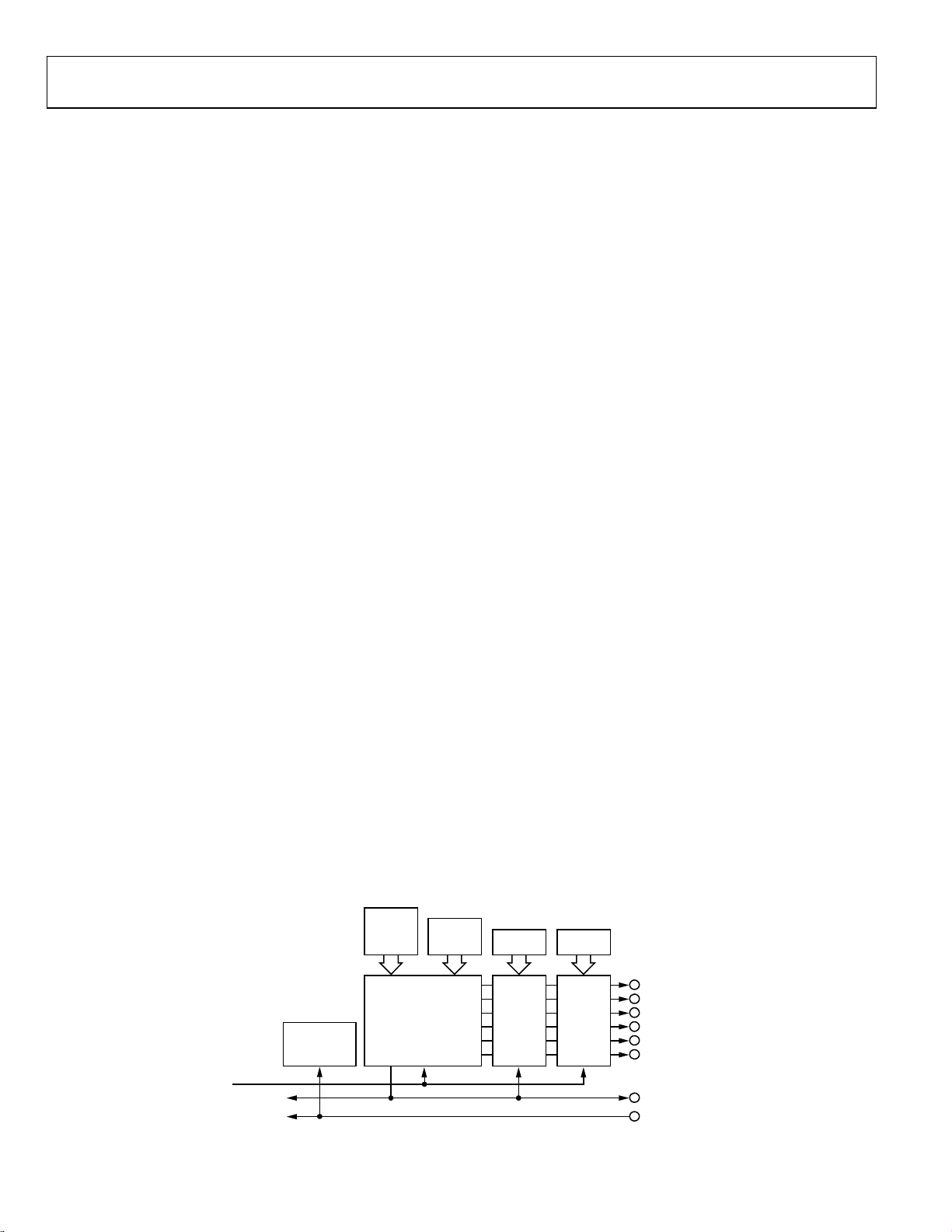
ADuC7019/20/21/22/24/25/26/27/28/29
T
DESCRIPTION OF THE PWM BLOCK
A functional block diagram of the PWM controller is shown in
Figure 58. The generation of the six output PWM signals on
Pin PWM0
important blocks:
• The 3-phase PWM timing unit. The core of the PWM
• The output control unit. This block can redirect the
• The gate drive unit. This block can generate the high
• The PWM shutdown controller. This block controls the
The PWM controller is driven by the ADuC7019/20/21/22/24/
25/26/27/28/29 core clock frequency and is capable of generating
two interrupts to the ARM core. One interrupt is generated on
the occurrence of a PWMSYNC pulse, and the other is
generated on the occurrence of any PWM shutdown action.
3-Phase Timing Unit
PWM Switching Frequency (PWMDAT0 MMR)
The PWM switching frequency is controlled by the PWM
period register, PWMDAT0. The fundamental timing unit of
the PWM controller is
where f
to Pin PWM2L is controlled by the following four
H
controller, this block generates three pairs of complemented
and dead-time-adjusted, center-based PWM signals. This
unit also generates the internal synchronization pulse,
PWMSYNC. It also controls whether the external PWM
SYNC
pin is used.
outputs of the 3-phase timing unit for each channel to
either the high-side or low-side output. In addition, the
output control unit allows individual enabling/disabling of
each of the six PWM output signals.
frequency chopping and its subsequent mixing with the
PWM signals.
PWM shutdown via the PWM
pin and generates the
TRIP
correct reset signal for the timing unit.
t
CORE
= 1/f
CORE
CORE
is the core frequency of the MicroConverter.
CONFIGURATION
REGISTERS
PWMCON
PWMDAT0
PWMDAT1
PWMDAT2
DUTY CYCL E
REGISTERS
PWMCH0
PWMCH1
PWMCH2
Therefore, for a 41.78 MHz f
, the fundamental time increment
CORE
is 24 ns. The value written to the PWMDAT0 register is effectively
the number of f
clock increments in one-half a PWM
CORE
period. The required PWMDAT0 value is a function of the
desired PWM switching frequency (f
PWMDAT0 = f
CORE
/(2 × f
PWM
Therefore, the PWM switching period, t
t
= 2 × PWMDAT0 × t
S
CORE
) and is given by
PWN
)
, can be written as
S
The largest value that can be written to the 16-bit PWMDAT0
MMR is 0xFFFF = 65,535, which corresponds to a minimum
PWM switching frequency of
f
= 41.78 × 10⁶/(2 × 65,535) = 318.75 Hz
PWM(min)
Note that PWMDAT0 values of 0 and 1 are not defined and
should not be used.
PWM Switching Dead Time (PWMDAT1 MMR)
The second important parameter that must be set up in the initial
configuration of the PWM block is the switching dead time. This
is a short delay time introduced between turning off one PWM
signal (0H, for example) and turning on the complementary
signal (0L). This short time delay is introduced to permit the
power switch to be turned off (in this case, 0H) to completely
recover its blocking capability before the complementary switch is
turned on. This time delay prevents a potentially destructive
short-circuit condition from developing across the dc link
capacitor of a typical voltage source inverter.
The dead time is controlled by the 10-bit, read/write PWMDAT1
register. There is only one dead-time register that controls the dead
time inserted into all three pairs of PWM output signals. The dead
time, t
, is related to the value in the PWMDAT1 register by
D
= PWMDAT1 × 2 × t
t
D
CORE
Therefore, a PWMDAT1 value of 0x00A (= 10), introduces
a 426 ns delay between the turn-off on any PWM signal (0H,
for example) and the turn-on of its complementary signal (0L).
The amount of the dead time can, therefore, be programmed in
increments of 2t
PWMEN
(or 49 ns for a 41.78 MHz core clock).
CORE
PWMCFG
PWM0
H
PWM0
PWM1
PWM1
PWM2
PWM2
PWM
PWM
L
H
L
H
L
SYNC
TRIP
04955-027
O INTERRUPT
CONTROLL ER
PWM
SHUTDOWN
CONTROLL ER
3-PHASE
PWM TIMING
UNIT
OUTPUT
CONTROL
UNIT
SYNCCORE CLOCK
GATE
DRIVE
UNIT
Figure 58. Overview of the PWM Controller
Rev. D | Page 58 of 96
Page 59
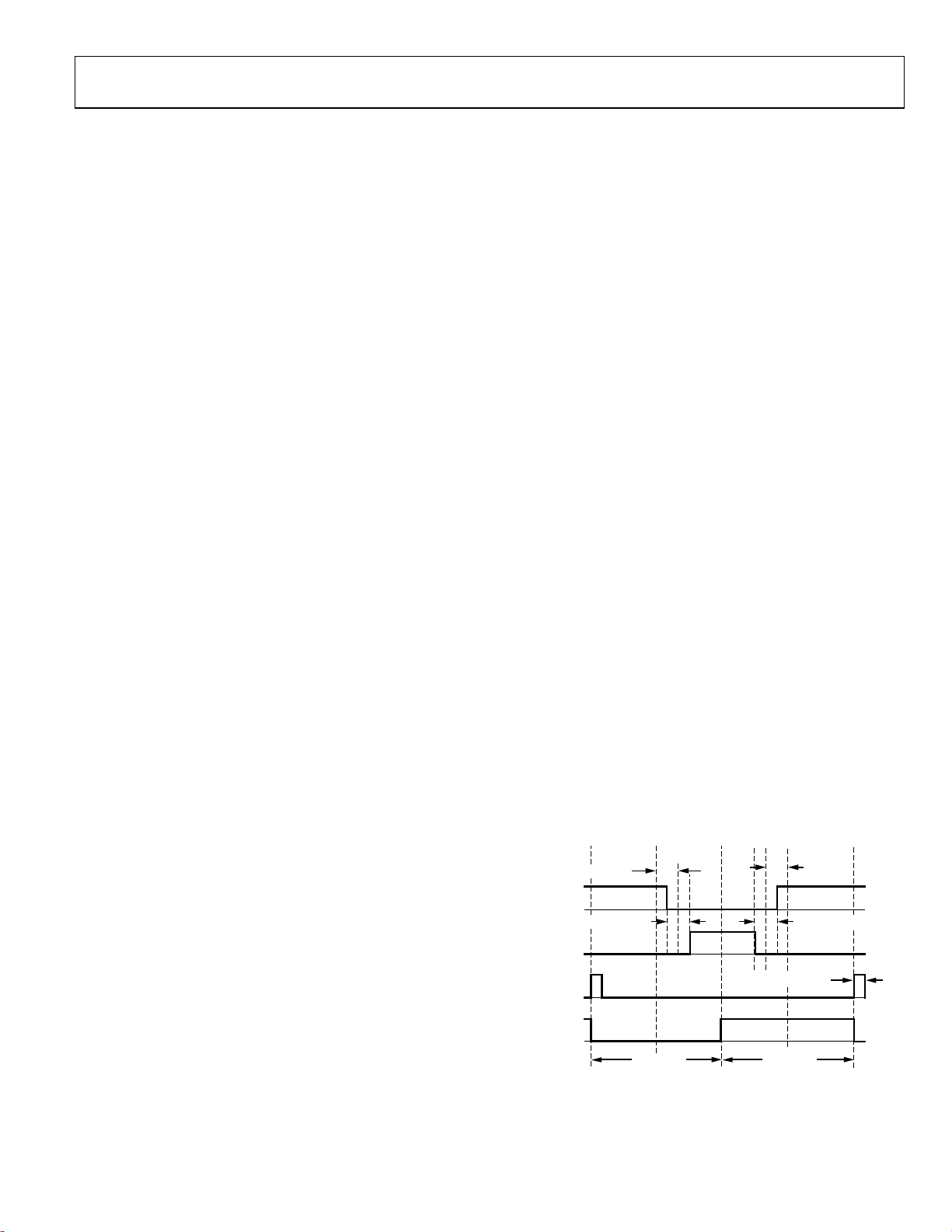
ADuC7019/20/21/22/24/25/26/27/28/29
–
–
The PWMDAT1 register is a 10-bit register with a maximum
value of 0x3FF (= 1023), which corresponds to a maximum
programmed dead time of
t
= 1023 × 2 × t
D(max)
= 1023 × 2 × 24 ×10–9 = 48.97 µs
CORE
for a core clock of 41.78 MHz.
The dead time can be programmed to be zero by writing 0 to
the PWMDAT1 register.
PWM Operating Mode (PWMCON and PWMSTA MMRs)
As discussed in the 3-Phase PWM section, the PWM controller
of the ADuC7019/20/21/22/24/25/26/27/28/29 can operate in
two distinct modes: single update mode and double update
mode. The operating mode of the PWM controller is
determined by the state of Bit 2 of the PWMCON register.
If this bit is cleared, the PWM operates in the single update
mode. Setting Bit 2 places the PWM in the double update
mode. The default operating mode is single update mode.
In single update mode, a single PWMSYNC pulse is produced
in each PWM period. The rising edge of this signal marks the
start of a new PWM cycle and is used to latch new values from
the PWM configuration registers (PWMDAT0 and PWMDAT1)
and the PWM duty cycle registers (PWMCH0, PWMCH1, and
PWMCH2) into the 3-phase timing unit. In addition, the
PWMEN register is latched into the output control unit on the
rising edge of the PWMSYNC pulse. In effect, this means that
the characteristics and resulting duty cycles of the PWM signals
can be updated only once per PWM period at the start of each
cycle. The result is symmetrical PWM patterns about the
midpoint of the switching period.
In double update mode, there is an additional PWMSYNC
pulse produced at the midpoint of each PWM period. The
rising edge of this new PWMSYNC pulse is again used to latch
new values of the PWM configuration registers, duty cycle
registers, and the PWMEN register. As a result, it is possible to
alter both the characteristics (switching frequency and dead
time) as well as the output duty cycles at the midpoint of each
PWM cycle. Consequently, it is also possible to produce PWM
switching patterns that are no longer symmetrical about the
midpoint of the period (asymmetrical PWM patterns). In
double update mode, it could be necessary to know whether
operation at any point in time is in either the first half or the
second half of the PWM cycle. This information is provided by
Bit 0 of the PWMSTA register, which is cleared during operation
in the first half of each PWM period (between the rising edge of
the original PWMSYNC pulse and the rising edge of the new
PWMSYNC pulse introduced in double update mode). Bit 0 of
the PWMSTA register is set during operation in the second half
of each PWM period. This status bit allows the user to make a
determination of the particular half cycle during implementation
of the PWMSYNC interrupt service routine, if required.
The advantage of double update mode is that lower harmonic
voltages can be produced by the PWM process, and faster
control bandwidths are possible. However, for a given PWM
switching frequency, the PWMSYNC pulses occur at twice the
rate in the double update mode. Because new duty cycle values
must be computed in each PWMSYNC interrupt service
routine, there is a larger computational burden on the ARM
core in double update mode.
PWM Duty Cycles (PWMCH0, PWMCH1, and PWMCH2 MMRs)
The duty cycles of the six PWM output signals on Pin PWM0H
to Pin PWM2
are controlled by the three 16-bit read/write duty
L
cycle registers, PWMCH0, PWMCH1, and PWMCH2. The
duty cycle registers are programmed in integer counts of the
fundamental time unit, t
. They define the desired on time of
CORE
the high-side PWM signal produced by the 3-phase timing unit
over half the PWM period. The switching signals produced by
the 3-phase timing unit are also adjusted to incorporate the
programmed dead time value in the PWMDAT1 register. The
3-phase timing unit produces active high signals so that a high
level corresponds to a command to turn on the associated
power device.
Figure 59 shows a typical pair of PWM outputs (in this case, 0H
and 0L) from the timing unit in single update mode. All
illustrated time values indicate the integer value in the
associated register and can be converted to time by simply
multiplying by the fundamental time increment, t
. Note that
CORE
the switching patterns are perfectly symmetrical about the
midpoint of the switching period in this mode because the same
values of PWMCH0, PWMDAT0, and PWMDAT1 are used to
define the signals in both half cycles of the period.
Figure 59 also demonstrates how the programmed duty cycles
are adjusted to incorporate the desired dead time into the
resulting pair of PWM signals. The dead time is incorporated
by moving the switching instants of both PWM signals (0H and
0L) away from the instant set by the PWMCH0 register.
PWMDAT0 ÷ 2
PWMCH0
0H
0L
PWMSYNC
PWMSTA (0)
PWMDAT0
Figure 59. Typical PWM Outputs of the 3-Phase Timing Unit
+PWMDAT0 ÷ 2
PWMDAT2 + 1
PWMDAT0
(Single Update Mode)
PWMDAT0 ÷ 200
PWMCH0
2 × PWMDAT12 × PW MDAT1
4955-028
Rev. D | Page 59 of 96
Page 60

ADuC7019/20/21/22/24/25/26/27/28/29
–
Both switching edges are moved by an equal amount
(PWMDAT1 × t
patterns.
Also shown are the PWMSYNC pulse and Bit 0 of the
PWMSTA register, which indicates whether operation is in the
first or second half cycle of the PWM period.
The resulting on times of the PWM signals over the full PWM
period (two half periods) produced by the timing unit can be
written as follows:
On the high side
t
= PWMDAT0 + 2(PWMCH0 − PWMDAT1) × t
0HH
= PWMDAT0 − 2(PWMCH0 − PWMDAT1) × t
t
0HL
and the corresponding duty cycles (d)
d
= t
0H
0HH/tS
and on the low side
t
= PWMDAT0 − 2(PWMCH0 + PWMDAT1) × t
0LH
t
= PWMDAT0 + 2(PWMCH0 + PWMDAT1) × t
0LL
and the corresponding duty cycles (d)
d
= t
OL
0LH/tS
The minimum permissible t
corresponding to a 0% duty cycle. In a similar fashion, the
maximum value is t
Figure 60 shows the output signals from the timing unit for
operation in double update mode. It illustrates a general case
where the switching frequency, dead time, and duty cycle are all
changed in the second half of the PWM period. The same value
for any or all of these quantities can be used in both halves of the
PWM cycle. However, there is no guarantee that symmetrical
PWM signals are produced by the timing unit in double update
mode. Figure 60 also shows that the dead time insertions into
the PWM signals are done in the same way as in single update
mode.
–PWMDAT01÷ 2
0H
2 × PWMDAT1
0L
PWMSYNC
PWMSTA (0)
Figure 60. Typical PWM Outputs of the 3-Phase Timing Unit
) to preserve the symmetrical output
CORE
= ½ + (PWMCH0 − PWMDAT1)/PWMDAT0
= ½ − (PWMCH0 + PWMDAT1)/PWMDAT0
and t0L values are zero,
0H
, corresponding to a 100% duty cycle.
S
PWMCH0
PWMDAT02÷ 2
00
+PWMDAT01÷ 2
1
1
PWMDAT22+ 1PWMDAT21+ 1
PWMDAT0
1
(Double Update Mode)
PWMDAT0
+PWMDAT0
PWMCH0
2 × PWMDAT1
2
CORE
CORE
CORE
2
CORE
2
÷ 2
2
04955-029
In general, the on times of the PWM signals in double update
mode can be defined as follows:
On the high side
t
= (PWMDAT0
0HH
PWMCH0
= (PWMDAT0
t
0HL
PWMCH0
− PWMDAT11 − PWMDAT12) × t
2
+ PWMDAT11 + PWMDAT12) × t
2
/2 + PWMDAT02/2 + PWMCH0
1
CORE
/2 + PWMDAT02/2 − PWMCH0
1
CORE
+
1
−
1
where Subscript 1 refers to the value of that register during the
first half cycle, and Subscript 2 refers to the value during the
second half cycle.
The corresponding duty cycles (d) are
d
= t
0H
PWMCH0
(PWMDAT0
= (PWMDAT0
0HH/tS
+ PWMCH02 − PWMDAT11 − PWMDAT12)/
1
+ PWMDAT02)
1
/2 + PWMDAT02/2 +
1
On the low side
t
= (PWMDAT0
0LH
PWMCH0
= (PWMDAT0
t
0LL
PWMCH0
+ PWMDAT11 + PWMDAT12) × t
2
− PWMDAT11 − PWMDAT12) × t
2
/2 + PWMDAT02/2 + PWMCH0
1
CORE
/2 + PWMDAT02/2 − PWMCH0
1
CORE
+
1
−
1
where Subscript 1 refers to the value of that register during the
first half cycle, and Subscript 2 refers to the value during the
second half cycle.
The corresponding duty cycles (d) are
d
= t
0L
PWMCH0
PWMDAT1
= (PWMDAT01/2 + PWMDAT02/2 +
0LH/tS
+ PWMCH02 + PWMDAT11 +
1
)/(PWMDAT01 + PWMDAT02)
2
For the completely general case in double update mode
(see Figure 60), the switching period is given by
tS = (PWMDAT0
+ PWMDAT02) × t
1
CORE
Again, the values of t0H and t0L are constrained to lie between
zero and t
.
S
PWM signals similar to those illustrated in Figure 59 and
Figure 60 can be produced on the 1H, 1L, 2H, and 2L outputs by
programming the PWMCH1 and PWMCH2 registers in a manner
identical to that described for PWMCH0. The PWM controller
does not produce any PWM outputs until all of the PWMDAT0,
PWMCH0, PWMCH1, and PWMCH2 registers have been written
to at least once. When these registers are written, internal
counting of the timers in the 3-phase timing unit is enabled.
Writing to the PWMDAT0 register starts the internal timing of
the main PWM timer. Provided that the PWMDAT0 register is
written to prior to the PWMCH0, PWMCH1, and PWMCH2
registers in the initialization, the first PWMSYNC pulse and
after the initial write to the PWMDAT0 register in single update
interrupt (if enabled) appear 1.5 × t
× PWMDAT0 seconds
CORE
mode. In double update mode, the first PWMSYNC pulse
appears after PWMDAT0 × t
seconds.
CORE
Rev. D | Page 60 of 96
Page 61
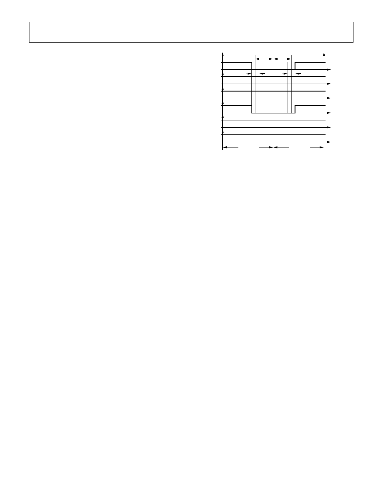
ADuC7019/20/21/22/24/25/26/27/28/29
Output Control Unit
The operation of the output control unit is controlled by the
9-bit read/write PWMEN register. This register controls two
distinct features of the output control unit that are directly
useful in the control of electronic counter measures (ECM) or
binary decimal counter measures (BDCM). The PWMEN
register contains three crossover bits, one for each pair of PWM
outputs. Setting Bit 8 of the PWMEN register enables the
crossover mode for the 0H/0L pair of PWM signals, setting
Bit 7 enables crossover on the 1H/1L pair of PWM signals, and
setting Bit 6 enables crossover on the 2H/2L pair of PWM
signals. If crossover mode is enabled for any pair of PWM
signals, the high-side PWM signal from the timing unit (0H, for
example) is diverted to the associated low-side output of the
output control unit so that the signal ultimately appears at the
PWM0
pin. Of course, the corresponding low-side output of
L
the timing unit is also diverted to the complementary high-side
output of the output control unit so that the signal appears at
the PWM0
pin. Following a reset, the three crossover bits are
H
cleared, and the crossover mode is disabled on all three pairs of
PWM signals. The PWMEN register also contains six bits (Bit 0
to Bit 5) that can be used to individually enable or disable each
of the six PWM outputs. If the associated bit of the PWMEN
register is set, the corresponding PWM output is disabled
regardless of the corresponding value of the duty cycle register.
This PWM output signal remains in the off state as long as the
corresponding enable/disable bit of the PWMEN register is set.
The implementation of this output enable function is implemented after the crossover function.
Following a reset, all six enable bits of the PWMEN register are
cleared, and all PWM outputs are enabled by default. In a manner
identical to the duty cycle registers, the PWMEN is latched on
the rising edge of the PWMSYNC signal. As a result, changes to
this register become effective only at the start of each PWM cycle
in single update mode. In double update mode, the PWMEN
register can also be updated at the midpoint of the PWM cycle.
In the control of an ECM, only two inverter legs are switched at
any time, and often the high-side device in one leg must be
switched on at the same time as the low-side driver in a second
leg. Therefore, by programming identical duty cycle values for
two PWM channels (for example, PWMCH0 = PWMCH1) and
setting Bit 7 of the PWMEN register to cross over the 1H/1L
pair of PWM signals, it is possible to turn on the high-side
switch of Phase A and the low-side switch of Phase B at the
same time. In the control of ECM, it is usual for the third
inverter leg (Phase C in this example) to be disabled for a
number of PWM cycles. This function is implemented by
disabling both the 2H and 2L PWM outputs by setting Bit 0
and Bit 1 of the PWMEN register.
This situation is illustrated in
Figure 61, where it can be seen
that both the 0H and 1L signals are identical because
PWMCH0 = PWMCH1 and the crossover bit for Phase B is set.
PWMCH0 =
PWMCH1
0H
0L
1H
1L
2H
2L
PWMDAT0 PWMDAT 0
Figure 61. Active Low PWM Signals Suitable for ECM Control,
PWMCH0 = PWMCH1, Crossover 1H/1L Pair and Disable
0L, 1H, 2H, and 2L Outputs in Single Update Mode.
PWMCH0 =
PWMCH1
2 × PWM DAT12 × PWMDAT1
04955-030
In addition, the other four signals (0L, 1H, 2H, and 2L) have
been disabled by setting the appropriate enable/disable bits of
the PWMEN register. In Figure 61, the appropriate value for
the PWMEN register is 0x00A7. In normal ECM operation,
each inverter leg is disabled for certain periods of time to
change the PWMEN register based on the position of the rotor
shaft (motor commutation).
Gate Drive Unit
The gate drive unit of the PWM controller adds features that
simplify the design of isolated gate-drive circuits for PWM
inverters. If a transformer-coupled, power device, gate-drive
amplifier is used, the active PWM signal must be chopped at a
high frequency. The 16-bit read/write PWMCFG register
programs this high frequency chopping mode. The chopped
active PWM signals can be required for the high-side drivers
only, the low-side drivers only, or both the high-side and lowside switches. Therefore, independent control of this mode for
both high-side and low-side switches is included with two
separate control bits in the PWMCFG register.
Typical PWM output signals with high frequency chopping
enabled on both high-side and low-side signals are shown in
Figure 62. Chopping of the high-side PWM outputs (0H, 1H,
and 2H) is enabled by setting Bit 8 of the PWMCFG register.
Chopping of the low-side PWM outputs (0L, 1L, and 2L) is
enabled by setting Bit 9 of the PWMCFG register. The high
chopping frequency is controlled by the 8-bit word (GDCLK)
placed in Bit 0 to Bit 7 of the PWMCFG register. The period of
this high frequency carrier is
t
= (4 × (GDCLK + 1)) × t
CHOP
CORE
The chopping frequency is, therefore, an integral subdivision of
the MicroConverter core frequency
f
= f
CHOP
/(4 × (GDCLK + 1))
CORE
Rev. D | Page 61 of 96
Page 62
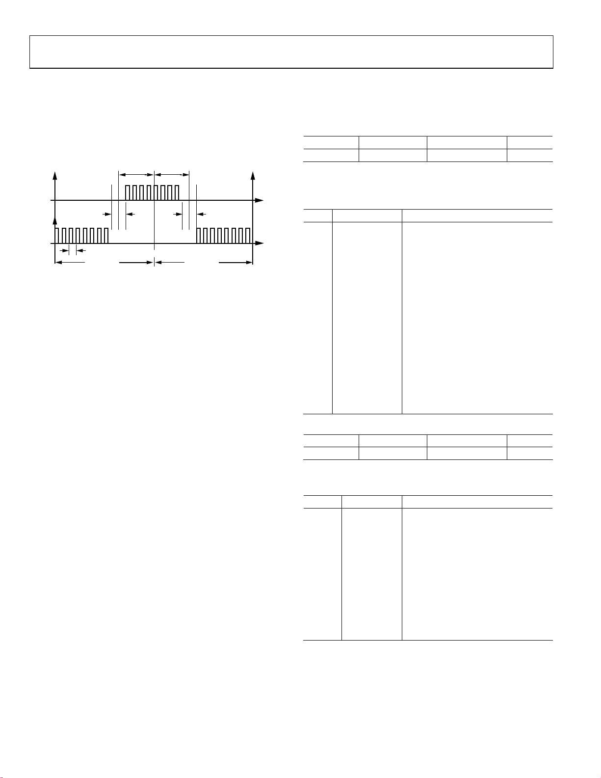
ADuC7019/20/21/22/24/25/26/27/28/29
The GDCLK value can range from 0 to 255, corresponding to a
programmable chopping frequency rate of 40.8 kHz to 10.44 MHz
for a 41.78 MHz core frequency. The gate drive features must be
programmed before operation of the PWM controller and are
typically not changed during normal operation of the PWM
controller. Following a reset, all bits of the PWMCFG register
are cleared so that high frequency chopping is disabled, by default.
PWMCH0 PWMCH0
0L
2 × PWMDAT1
0H
4 × (GDCLK + 1) ×
Figure 62. Typical PWM Signals with High Frequency Gate Chopping
Enabled on Both High-Side and Low-Side Switches
t
CORE
PWM Shutdown
In the event of external fault conditions, it is essential that the
PWM system be instantaneously shut down in a safe fashion. A
low level on the PWM
pin provides an instantaneous,
TRIP
asynchronous (independent of the MicroConverter core clock)
shutdown of the PWM controller. All six PWM outputs are
placed in the off state, that is, in low state. In addition, the
PWMSYNC pulse is disabled. The PWM
pull-down resistor to disable the PWM if the pin becomes
disconnected. The state of the PWM
Bit 3 of the PWMSTA register.
TRIP
If a PWM shutdown command occurs, a PWMTRIP interrupt is
generated, and internal timing of the 3-phase timing unit of the
PWM controller is stopped. Following a PWM shutdown, the
PWM can be reenabled (in a PWMTRIP interrupt service
routine, for example) only by writing to all of the PWMDAT0,
PWMCH0, PWMCH1, and PWMCH2 registers. Provided that
the external fault is cleared and the PWMTRIP is returned to a
high level, the internal timing of the 3-phase timing unit
resumes, and new duty-cycle values are latched on the next
PWMSYNC boundary.
Note that the PWMTRIP interrupt is available in IRQ only,
and the PWMSYNC interrupt is available in FIQ only. Both
interrupts share the same bit in the interrupt controller.
Therefore, only one of the interrupts can be used at a time.
See the Interrupt System section for further details.
2 × PWMDAT1
PWMDAT0PWMDAT0
pin has an internal
TRIP
pin can be read from
4955-031
PWM MMRs Interface
The PWM block is controlled via the MMRs described in
this section.
Table 66. PWMCON Register
Name Address Default Value Access
PWMCON 0xFFFFFC00 0x0000 R/W
PWMCON is a control register that enables the PWM and
chooses the update rate.
Table 67. PWMCON MMR Bit Descriptions
Bit Name Description
7:5 Reserved.
4 PWM_SYNCSEL
External sync select. Set to use external
sync. Cleared to use internal sync.
3 PWM_EXTSYNC
External sync select. Set to select
external synchronous sync signal.
Cleared for asynchronous sync signal.
2 PWMDBL
Double update mode. Set to 1 by user
to enable double update mode.
Cleared to 0 by the user to enable
single update mode.
1 PWM_SYNC_EN
PWM synchronization enable. Set by
user to enable synchronization. Cleared
by user to disable synchronization.
0 PWMEN
PWM enable bit. Set to 1 by user to
enable the PWM. Cleared to 0 by user
to disable the PWM. Also cleared
automatically with PWMTRIP
(PWMSTA MMR).
Table 68. PWMSTA Register
Name Address Default Value Access
PWMSTA 0xFFFFFC04 0x0000 R/W
PWMSTA reflects the status of the PWM.
Table 69. PWMSTA MMR Bit Descriptions
Bit Name Description
15:10 Reserved.
9 PWMSYNCINT
PWM sync interrupt bit. Writing a 1 to
this bit clears this interrupt.
8 PWMTRIPINT
PWM trip interrupt bit. Writing a 1 to
this bit clears this interrupt.
3 PWMTRIP
2:1
0 PWMPHASE
Raw signal from the PWM
Reserved.
PWM phase bit. Set to 1 by the Micro-
TRIP
pin.
Converter when the timer is counting
down (first half). Cleared to 0 by the
MicroConverter when the timer is
counting up (second half).
Rev. D | Page 62 of 96
Page 63
ADuC7019/20/21/22/24/25/26/27/28/29
Table 70. PWMCFG Register
Name Address Default Value Access
PWMCFG 0xFFFFFC10 0x0000 R/W
PWMCFG is a gate chopping register.
Table 71. PWMCFG MMR Bit Descriptions
Bit Name Description
15:10 Reserved.
9 CHOPLO Low-side gate chopping enable bit.
8 CHOPHI High-side gate chopping enable bit.
7:0 GDCLK PWM gate chopping period (unsigned).
Table 72. PWMEN Register
Name Address Default Value Access
PWMEN 0xFFFFFC20 0x0000 R/W
PWMEN allows enabling of channel outputs and crossover. See
its bit definitions in Tabl e 73 .
Table 73. PWMEN MMR Bit Descriptions
Bit Name Description
8 0H0L_XOVR
7 1H1L_XOVR
6 2H2L_XOVR
5 0L_EN
4 0H_EN
3 1L_EN
2 1H_EN
1 2L_EN
0 2H_EN
Channel 0 output crossover enable bit.
Set to 1 by user to enable Channel 0 output
crossover. Cleared to 0 by user to disable
Channel 0 output crossover.
Channel 1 output crossover enable bit.
Set to 1 by user to enable Channel 1 output
crossover. Cleared to 0 by user to disable
Channel 1 output crossover.
Channel 2 output crossover enable bit.
Set to 1 by user to enable Channel 2 output
crossover. Cleared to 0 by user to disable
Channel 2 output crossover.
0L output enable bit. Set to 1 by user to
disable the 0L output of the PWM. Cleared to 0
by user to enable the 0L output of the PWM.
0H output enable bit. Set to 1 by user to
disable the 0H output of the PWM. Cleared to
0 by user to enable the 0H output of the PWM.
1L output enable bit. Set to 1 by user to
disable the 1L output of the PWM. Cleared to 0
by user to enable the 1L output of the PWM.
1H Output Enable Bit. Set to 1 by user to
disable the 1H output of the PWM. Cleared to
0 by user to enable the 1H output of the PWM.
2L output enable bit. Set to 1 by user to
disable the 2L output of the PWM. Cleared to 0
by user to enable the 2L output of the PWM.
2H output enable bit. Set to 1 by user to
disable the 2H output of the PWM. Cleared to
0 by user to enable the 2H output of the PWM.
Table 74. PWMDAT0 Register
Name Address Default Value Access
PWMDAT0 0xFFFFFC08 0x0000 R/W
PWMDAT0 is an unsigned 16-bit register for switching period.
Table 75. PWMDAT1 Register
Name Address Default Value Access
PWMDAT1 0xFFFFFC0C 0x0000 R/W
PWMDAT1 is an unsigned 10-bit register for dead time.
Table 76. PWMCHx Registers
Name Address Default Value Access
PWMCH0 0xFFFFFC14 0x0000 R/W
PWMCH1 0xFFFFFC18 0x0000 R/W
PWMCH2 0xFFFFFC1C 0x0000 R/W
PWMCH0, PWMCH1, and PWMCH2 are channel duty cycles
for the three phases.
Table 77. PWMDAT2 Register
Name Address Default Value Access
PWMDAT2 0xFFFFFC24 0x0000 R/W
PWMDAT2 is an unsigned 10-bit register for PWM sync
pulse width.
GENERAL-PURPOSE INPUT/OUTPUT
The ADuC7019/20/21/22/24/25/26/27/28/29 provide 40 generalpurpose, bidirectional I/O (GPIO) pins. All I/O pins are 5 V
tolerant, meaning the GPIOs support an input voltage of 5 V.
In general, many of the GPIO pins have multiple functions (see
Tabl e 7 8 for the pin function definitions). By default, the GPIO
pins are configured in GPIO mode.
All GPIO pins have an internal pull-up resistor (of about
100 kΩ), and their drive capability is 1.6 mA. Note that a
maximum of 20 GPIOs can drive 1.6 mA at the same time.
Using the GPxPAR registers, it is possible to enable/disable
the pull-up resistors for the following ports: P0.0, P0.4, P0.5,
P0.6, P0.7, and the eight GPIOs of P1.
The 40 GPIOs are grouped in five ports, Port 0 to Port 4 (Port x).
Each port is controlled by four or five MMRs.
Note that the kernel changes P0.6 from its default configuration
at reset (MRST) to GPIO mode. If MRST is used for external
circuitry, an external pull-up resistor should be used to ensure
that the level on P0.6 does not drop when the kernel switches
mode. Otherwise, P0.6 goes low for the reset period. For
example, if MRST is required for power-down, it can be
reconfigured in GP0CON MMR.
The input level of any GPIO can be read at any time in the
GPxDAT MMR, even when the pin is configured in a mode
other than GPIO. The PLA input is always active.
When the ADuC7019/20/21/22/24/25/26/27/28/29 part enters a
power-saving mode, the GPIO pins retain their state.
Rev. D | Page 63 of 96
Page 64
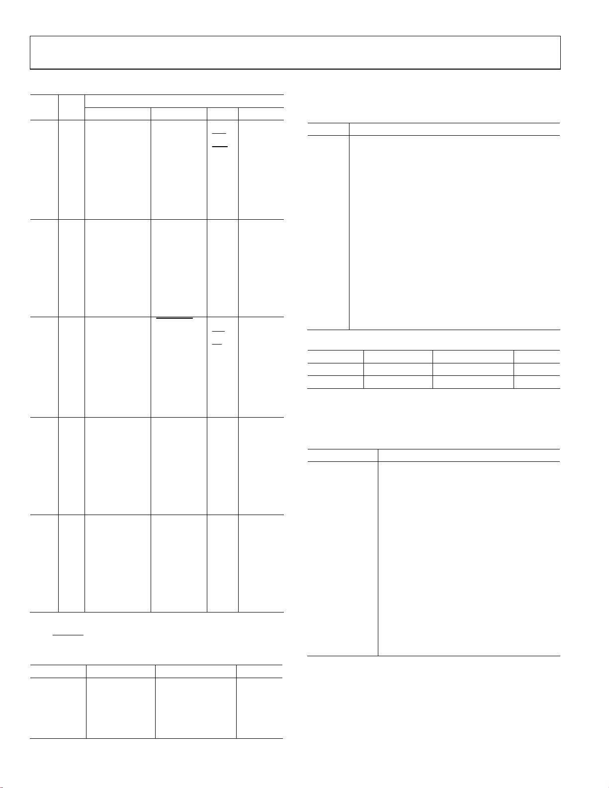
ADuC7019/20/21/22/24/25/26/27/28/29
Table 78. GPIO Pin Function Descriptions
Configuration
Port Pin 00 01 10 11
0 P0.0 GPIO CMP MS0 PLAI[7]
BUSY
PLAO[6]
PLAO[7]
Rev. D | Page 64 of 96
P0.1 GPIO PWM2H
P0.2 GPIO PWM2L
BLE
BHE
P0.3 GPIO TRST A16 ADC
P0.4 GPIO/IRQ0 PWM
P0.5 GPIO/IRQ1 ADC
MS1 PLAO[1]
TRIP
MS2 PLAO[2]
BUSY
P0.6 GPIO/T1 MRST PLAO[3]
P0.7 GPIO ECLK/XCLK1 SIN PLAO[4]
1 P1.0 GPIO/T1 SIN SCL0 PLAI[0]
P1.1 GPIO SOUT SDA0 PLAI[1]
P1.2 GPIO RTS SCL1 PLAI[2]
P1.3 GPIO CTS SDA1 PLAI[3]
P1.4 GPIO/IRQ2 RI CLK PLAI[4]
P1.5 GPIO/IRQ3 DCD MISO PLAI[5]
P1.6 GPIO DSR MOSI PLAI[6]
P1.7 GPIO DTR CSL PLAO[0]
2
2 P2.0 GPIO
CONV
P2.1 GPIO PWM0H
P2.2 GPIO PWM0L
START
SOUT PLAO[5]
WS
RS
P2.3 GPIO AE
P2.4 GPIO PWM0H MS0
P2.5 GPIO PWM0L MS1
P2.6 GPIO PWM1H MS2
P2.7 GPIO PWM1L MS3
3 P3.0 GPIO PWM0H AD0 PLAI[8]
P3.1 GPIO PWM0L AD1 PLAI[9]
P3.2 GPIO PWM1H AD2 PLAI[10]
P3.3 GPIO PWM1L AD3 PLAI[11]
P3.4 GPIO PWM2H AD4 PLAI[12]
P3.5 GPIO PWM2L AD5 PLAI[13]
P3.6 GPIO PWM
P3.7 GPIO PWM
AD6 PLAI[14]
TRIP
AD7 PLAI[15]
SYNC
4 P4.0 GPIO AD8 PLAO[8]
P4.1 GPIO AD9 PLAO[9]
P4.2 GPIO AD10 PLAO[10]
P4.3 GPIO AD11 PLAO[11]
P4.4 GPIO AD12 PLAO[12]
P4.5 GPIO AD13 PLAO[13]
P4.6 GPIO AD14 PLAO[14]
P4.7 GPIO AD15 PLAO[15]
1
When configured in Mode 1, P0.7 is ECLK by default, or core clock output. To
configure it as a clock input, the MDCLK bits in PLLCON must be set to 11.
2
CONV
The
START
signal is active in all modes of P2.0.
Table 79. GPxCON Registers
Name Address Default Value Access
GP0CON 0xFFFFF400 0x00000000 R/W
GP1CON 0xFFFFF404 0x00000000 R/W
GP2CON 0xFFFFF408 0x00000000 R/W
GP3CON 0xFFFFF40C 0x00000000 R/W
GP4CON 0xFFFFF410 0x00000000 R/W
GPxCON are the Port x control registers, which select the
function of each pin of Port x as described in Tabl e 80 .
Table 80. GPxCON MMR Bit Descriptions
Bit Description
31:30 Reserved.
29:28 Select function of the Px.7 pin.
27:26 Reserved.
25:24 Select function of the Px.6 pin.
23:22 Reserved.
21:20 Select function of the Px.5 pin.
19:18 Reserved.
17:16 Select function of the Px.4 pin.
15:14 Reserved.
13:12 Select function of the Px.3 pin.
11:10 Reserved.
9:8 Select function of the Px.2 pin.
7:6 Reserved.
5:4 Select function of the Px.1 pin.
3:2 Reserved.
1:0 Select function of the Px.0 pin.
Table 81. GPxPAR Registers
Name Address Default Value Access
GP0PAR 0xFFFFF42C 0x20000000 R/W
GP1PAR 0xFFFFF43C 0x00000000 R/W
GPxPAR program the parameters for Port 0 and Port 1. Note that
the GPxDAT MMR must always be written after changing the
GPxPAR MMR.
Table 82. GPxPAR MMR Bit Descriptions
Bit Description
31:29 Reserved.
28 Pull-Up Disable Px.7.
27:25 Reserved.
24 Pull-Up Disable Px.6.
23:21 Reserved.
20 Pull-Up Disable Px.5.
19:17 Reserved.
16 Pull-Up Disable Px.4.
15:13 Reserved.
12 Pull-Up Disable Px.3.
11:9 Reserved.
8 Pull-Up Disable Px.2.
7:5 Reserved.
4 Pull-Up Disable Px.1.
3:1 Reserved.
0 Pull-Up Disable Px.0.
Page 65

ADuC7019/20/21/22/24/25/26/27/28/29
Table 83. GPxDAT Registers
Name Address Default Value
1
Access
GP0DAT 0xFFFFF420 0x000000XX R/W
GP1DAT 0xFFFFF430 0x000000XX R/W
GP2DAT 0xFFFFF440 0x000000XX R/W
GP3DAT 0xFFFFF450 0x000000XX R/W
GP4DAT 0xFFFFF460 0x000000XX R/W
1
X = 0, 1, 2, or 3.
GPxDAT are Port x configuration and data registers. They
configure the direction of the GPIO pins of Port x, set the
output value for the pins configured as output, and store the
input value of the pins configured as input.
Table 84. GPxDAT MMR Bit Descriptions
Bit Description
31:24
Direction of the data. Set to 1 by user to configure
the GPIO pin as an output. Cleared to 0 by user to
configure the GPIO pin as an input.
23:16 Port x data output.
15:8 Reflect the state of Port x pins at reset (read only).
7:0 Port x data input (read only).
Table 85. GPxSET Registers
Name Address Default Value
1
Access
GP0SET 0xFFFFF424 0x000000XX W
GP1SET 0xFFFFF434 0x000000XX W
GP2SET 0xFFFFF444 0x000000XX W
GP3SET 0xFFFFF454 0x000000XX W
GP4SET 0xFFFFF464 0x000000XX W
1
X = 0, 1, 2, or 3.
GPxSET are data set Port x registers.
Table 86. GPxSET MMR Bit Descriptions
Bit Description
31:24 Reserved.
23:16
Data Port x set bit. Set to 1 by user to set bit on Port x;
also sets the corresponding bit in the GPxDAT MMR.
Cleared to 0 by user; does not affect the data out.
15:0 Reserved.
Table 87. GPxCLR Registers
Name Address Default Value
1
Access
GP0CLR 0xFFFFF428 0x000000XX W
GP1CLR 0xFFFFF438 0x000000XX W
GP2CLR 0xFFFFF448 0x000000XX W
GP3CLR 0xFFFFF458 0x000000XX W
GP4CLR 0xFFFFF468 0x000000XX W
1
X = 0, 1, 2, or 3.
GPxCLR are data clear Port x registers.
Table 88. GPxCLR MMR Bit Descriptions
Bit Description
31:24 Reserved.
23:16
Data Port x clear bit. Set to 1 by user to clear bit on
Port x; also clears the corresponding bit in the GPxDAT
MMR. Cleared to 0 by user; does not affect the data out.
15:0 Reserved.
SERIAL PORT MUX
The serial port mux multiplexes the serial port peripherals
(an SPI, UART, and two I
(PLA) to a set of 10 GPIO pins. Each pin must be configured to
one of its specific I/O functions as described in Tab l e 8 9 .
Table 89. SPM Configuration
GPIO UART UART/I2C/SPI PLA
SPMMUX
(00) (01) (10) (11)
SPM0 P1.0 SIN I2C0SCL PLAI[0]
SPM1 P1.1 SOUT I2C0SDA PLAI[1]
SPM2 P1.2 RTS I2C1SCL PLAI[2]
SPM3 P1.3 CTS I2C1SDA PLAI[3]
SPM4 P1.4 RI SPICLK PLAI[4]
SPM5 P1.5 DCD SPIMISO PLAI[5]
SPM6 P1.6 DSR SPIMOSI PLAI[6]
SPM7 P1.7 DTR SPICSL PLAO[0]
SPM8 P0.7 ECLK/XCLK SIN PLAO[4]
SPM9 P2.0 CONV SOUT PLAO[5]
Tabl e 8 9 also details the mode for each of the SPMMUX pins.
This configuration must be done via the GP0CON, GP1CON,
and GP2CON MMRs. By default, these 10 pins are configured
as GPIOs.
2
Cs) and the programmable logic array
UART SERIAL INTERFACE
The UART peripheral is a full-duplex, universal, asynchronous
receiver/transmitter. It is fully compatible with the 16,450 serial
port standard. The UART performs serial-to-parallel conversions
on data characters received from a peripheral device or modem,
and parallel-to-serial conversions on data characters received
from the CPU. The UART includes a fractional divider for baud
rate generation and has a network addressable mode. The UART
function is made available on the 10 pins of the ADuC7019/20/
21/22/24/25/26/27/28/29 (see Tabl e 90 ).
Table 90. UART Signal Description
Pin Signal Description
SPM0 (Mode 1) SIN Serial receive data.
SPM1 (Mode 1) SOUT Serial transmit data.
SPM2 (Mode 1) RTS Request to send.
SPM3 (Mode 1) CTS Clear to send.
SPM4 (Mode 1) RI Ring indicator.
SPM5 (Mode 1) DCD Data carrier detect.
SPM6 (Mode 1) DSR Data set ready.
SPM7 (Mode 1) DTR Data terminal ready.
SPM8 (Mode 2) SIN Serial receive data.
SPM9 (Mode 2) SOUT Serial transmit data.
Rev. D | Page 65 of 96
Page 66
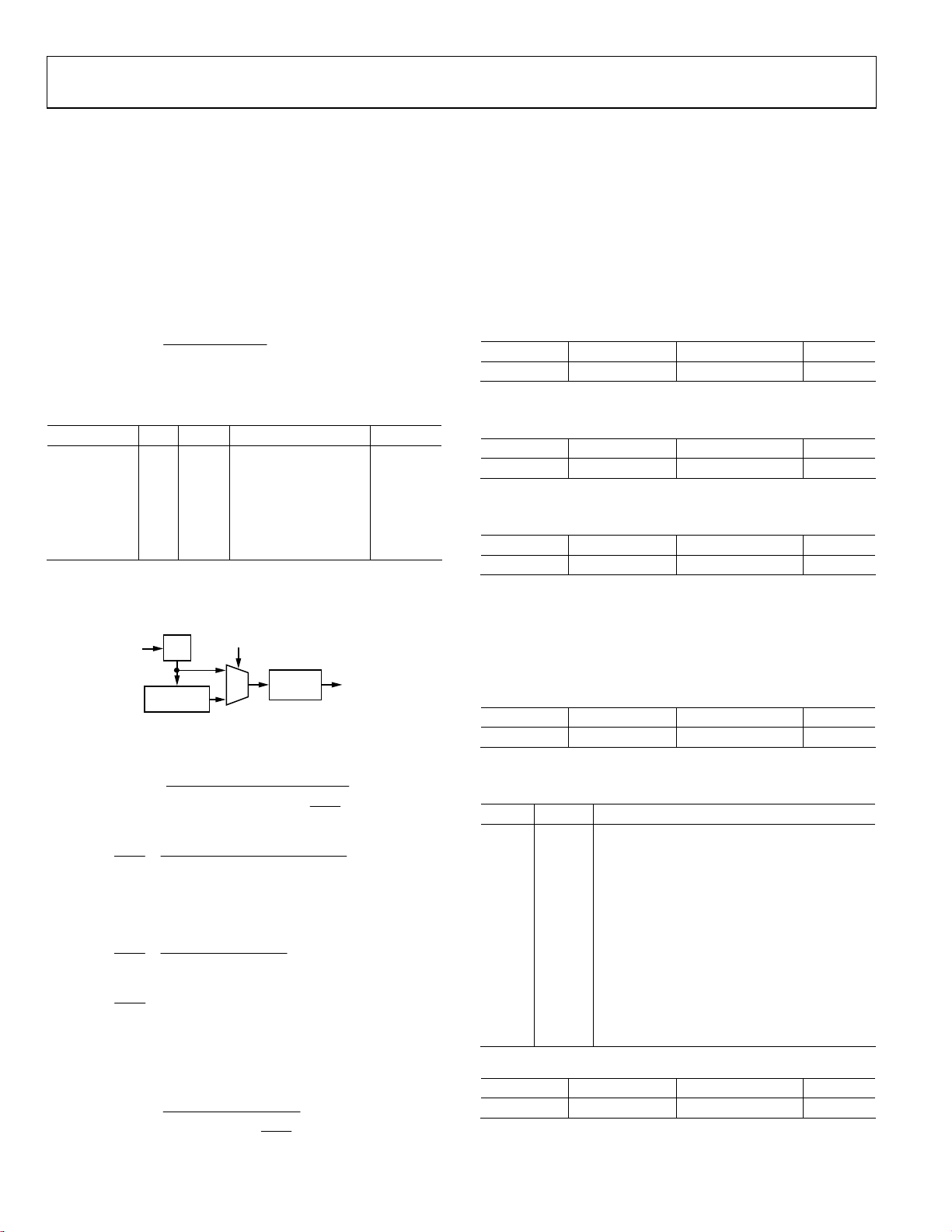
ADuC7019/20/21/22/24/25/26/27/28/29
The serial communication adopts an asynchronous protocol,
which supports various word lengths, stop bits, and parity
generation options selectable in the configuration register.
Baud Rate Generation
There are two ways of generating the UART baud rate, normal
450 UART baud rate generation and the fractional divider.
Normal 450 UART Baud Rate Generation
The baud rate is a divided version of the core clock using the values
in the COMDIV0 and COMDIV1 MMRs (16-bit value, DL).
RateBaud
=
Tabl e 9 1 gives some common baud rate values.
Table 91. Baud Rate Using the Normal Baud Rate Generator
Baud Rate CD DL Actual Baud Rate % Error
9600 0 0x88 9600 0
19,200 0 0x44 19,200 0
115,200 0 0x0B 118,691 3
9600 3 0x11 9600 0
19,200 3 0x08 20,400 6.25
115,200 3 0x01 163,200 41.67
Fractional Divider
The fractional divider, combined with the normal baud rate
generator, produces a wider range of more accurate baud rates.
CORE
CLOCK
/(M+N/2048)
Figure 63. Baud Rate Generation Options
Calculation of the baud rate using fractional divider is as follows:
=
RateBaud
N
2048
=+
M
For example, generation of 19,200 baud with CD bits = 3
(Tabl e 9 1 gives DL = 0x08) is
=+NM
2048
06.1
=+NM
2048
where:
M = 1
N = 0.06 × 2048 = 128
RateBaud
=
CD
/2
3
CD
MHz78.41
×××
2162
FBEN
DL
/16DL UART
MHz78.41
⎛
2162
MDL
⎜
⎝
+××××
N
2048
04955-032
⎞
⎟
⎠
MHz78.41
CD
MHz78.41
3
2816219200
××××
2162
××××
DLRateBaud
MHz78.41
⎛
××××
28162
⎜
⎝
128
2048
⎞
⎟
⎠
Rev. D | Page 66 of 96
where:
Baud Rate = 19,200 bps
Error = 0%, compared to 6.25% with the normal baud rate
generator.
UART Register Definitions
The UART interface consists of 12 registers: COMTX, COMRX,
COMDIV0, COMIEN0, COMDIV1, COMIID0, COMCON0,
COMCON1, COMSTA0, COMSTA1, COMSCR, and
COMDIV2.
Table 92. COMTX Register
Name Address Default Value Access
COMTX 0xFFFF0700 0x00 R/W
COMTX is an 8-bit transmit register.
Table 93. COMRX Register
Name Address Default Value Access
COMRX 0xFFFF0700 0x00 R
COMRX is an 8-bit receive register.
Table 94. COMDIV0 Register
Name Address Default Value Access
COMDIV0 0xFFFF0700 0x00 R/W
COMDIV0 is a low byte divisor latch. COMTX, COMRX,
and COMDIV0 share the same address location. COMTX
and COMRX can be accessed when Bit 7 in the COMCON0
register is cleared. COMDIV0 can be accessed when Bit 7
of COMCON0 is set.
Table 95. COMIEN0 Register
Name Address Default Value Access
COMIEN0 0xFFFF0704 0x00 R/W
COMIEN0 is the interrupt enable register.
Table 96. COMIEN0 MMR Bit Descriptions
Bit Name Description
7:4 N/A Reserved.
3 EDSSI
2 ELSI
1 ETBEI
0 ERBFI
Modem status interrupt enable bit. Set by
user to enable generation of an interrupt if
any of COMSTA1[3:1] is set. Cleared by user.
Rx status interrupt enable bit. Set by user to
enable generation of an interrupt if any of
COMSTA0[3:0] is set. Cleared by user.
Enable transmit buffer empty interrupt. Set
by user to enable interrupt when buffer is
empty during a transmission. Cleared by user.
Enable receive buffer full interrupt. Set by
user to enable interrupt when buffer is full
during a reception. Cleared by user.
Table 97. COMDIV1 Register
Name Address Default Value Access
COMDIV1 0xFFFF0704 0x00 R/W
COMDIV1 is a divisor latch (high byte) register.
Page 67
ADuC7019/20/21/22/24/25/26/27/28/29
Table 98. COMIID0 Register
Name Address Default Value Access
COMIID0 0xFFFF0708 0x01 R
COMIID0 is the interrupt identification register.
Table 99. COMIID0 MMR Bit Descriptions
Bit 2:1
Status Bits
00 1 N/A No interrupt N/A
11 0 1
10 0 2
01 0 3
00 0 4
Bit 0
NINT
Priority Definition
Receive line
status
interrupt
Receive buffer
full interrupt
Transmit
buffer empty
interrupt
Modem status
interrupt
Clearing
Operation
Read
COMSTA0
Read COMRX
Write data to
COMTX or
read COMIID
Read
COMSTA1
Table 100. COMCON0 Register
Name Address Default Value Access
COMCON0 0xFFFF070C 0x00 R/W
COMCON0 is the line control register.
Table 101. COMCON0 MMR Bit Descriptions
Bit Name Description
7 DLAB
6 BRK
5 SP
4 EPS
3 PEN
2 STOP
1:0 WLS
Divisor latch access. Set by user to enable
access to the COMDIV0 and COMDIV1
registers. Cleared by user to disable access to
COMDIV0 and COMDIV1 and enable access to
COMRX and COMTX.
Set break. Set by user to force SOUT to 0.
Cleared to operate in normal mode.
Stick parity. Set by user to force parity to
defined values: 1 if EPS = 1 and PEN = 1,
0 if EPS = 0 and PEN = 1.
Even parity select bit. Set for even parity.
Cleared for odd parity.
Parity enable bit. Set by user to transmit and
check the parity bit. Cleared by user for no
parity transmission or checking.
Stop bit. Set by user to transmit 1.5 stop bits if the
word length is five bits or 2 stop bits if the
word length is six bits, seven bits, or eight bits.
The receiver checks the first stop bit only,
regardless of the number of stop bits selected.
Cleared by user to generate 1 stop bit in the
transmitted data.
Word length select:
00 = five bits, 01 = six bits, 10 = seven bits,
11 = eight bits.
Table 102. COMCON1 Register
Name Address Default Value Access
COMCON1 0xFFFF0710 0x00 R/W
COMCON1 is the modem control register.
Table 103. COMCON1 MMR Bit Descriptions
Bit Name Description
7:5 Reserved.
4 LOOPBACK
3 PEN
2 STOP
1 RTS
0 DTR
Loopback. Set by user to enable loopback
mode. In loopback mode, SOUT (see Tabl e 78)
is forced high. The modem signals are also
directly connected to the status inputs (RTS
to CTS and DTR to DSR). Cleared by user to
be in normal mode.
Parity enable bit. Set by user to transmit and
check the parity bit. Cleared by user for no
parity transmission or checking.
Stop bit. Set by user to transmit 1.5 stop bits
if the word length is five bits, or 2 stop bits if
the word length is six bits, seven bits, or
eight bits. The receiver checks the first stop
bit only, regardless of the number of stop bits
selected. Cleared by user to generate 1 stop
bit in the transmitted data.
Request to send. Set by user to force the RTS
output to 0. Cleared by user to force the RTS
output to 1.
Data terminal ready. Set by user to force the
DTR output to 0. Cleared by user to force the
DTR output to 1.
Table 104. COMSTA0 Register
Name Address Default Value Access
COMSTA0 0xFFFF0714 0x60 R
COMSTA0 is the line status register.
Table 105. COMSTA0 MMR Bit Descriptions
Bit Name Description
7 Reserved.
6 TEMT
5 THRE
4 BI
3 FE
2 PE
1 OE
0 DR
COMTX and shift register empty status bit. Set
automatically if COMTX and shift register are
empty. Cleared automatically when writing to
COMTX.
COMTX empty. Set automatically if COMTX is
empty. Cleared automatically when writing to
COMTX.
Break error. Set when SIN is held low for more than
the maximum word length. Cleared automatically.
Framing error. Set when an invalid stop bit occurs.
Cleared automatically.
Parity error. Set when a parity error occurs.
Cleared automatically.
Overrun error. Set automatically if data is overwritten before being read. Cleared automatically.
Data ready. Set automatically when COMRX is full.
Cleared by reading COMRX.
Table 106. COMSTA1 Register
Name Address Default Value Access
COMSTA1 0xFFFF0718 0x00 R
COMSTA1 is a modem status register.
Rev. D | Page 67 of 96
Page 68

ADuC7019/20/21/22/24/25/26/27/28/29
Table 107. COMSTA1 MMR Bit Descriptions
Bit Name Description
7 DCD Data carrier detect.
6 RI Ring indicator.
5 DSR Data set ready.
4 CTS Clear to send.
3 DDCD
2 TERI
1 DDSR
0 DCTS
Delta DCD. Set automatically if DCD changed
state since last COMSTA1 read. Cleared automatically by reading COMSTA1.
Trailing edge RI. Set if RI changed from 0 to 1
since COMSTA1 was last read. Cleared
automatically by reading COMSTA1.
Delta DSR. Set automatically if DSR changed state
since COMSTA1 was last read. Cleared
automatically by reading COMSTA1.
Delta CTS. Set automatically if CTS changed state
since COMSTA1 was last read. Cleared
automatically by reading COMSTA1.
Network Addressable UART Register Definitions
Four additional registers, COMIEN0, COMIEN1, COMIID1, and
COMADR are used in network addressable UART mode only.
In network address mode, the least significant bit of the COMIEN1
register is the transmitted network address control bit. If set to
1, the device is transmitting an address. If cleared to 0, the
device is transmitting data. For example, the following masterbased code transmits the slave’s address followed by the data:
COMIEN1 = 0xE7; //Setting ENAM,
E9BT, E9BR, ETD, NABP
COMTX = 0xA0; // Slave address is 0xA0
while(!(0x020==(COMSTA0 & 0x020))){} //
wait for adr tx to finish.
COMIEN1 = 0xE6; // Clear NAB bit
to indicate Data is coming
COMTX = 0x55; // Tx data to slave: 0x55
Table 108. COMSCR Register
Name Address Default Value Access
COMSCR 0xFFFF071C 0x00 R/W
COMSCR is an 8-bit scratch register used for temporary
storage. It is also used in network addressable UART mode.
Table 109. COMDIV2 Register
Name Address Default Value Access
COMDIV2 0xFFFF072C 0x0000 R/W
COMDIV2 is a 16-bit fractional baud divide register.
Table 110. COMDIV2 MMR Bit Descriptions
Bit Name Description
15 FBEN
14:13 Reserved.
12:11 FBM[1:0]
10:0 FBN[10:0] N (see the Fractional Divider section).
Fractional baud rate generator enable bit.
Set by user to enable the fractional baud
rate generator. Cleared by user to generate
baud rate using the standard 450 UART
baud rate generator.
M if FBM = 0, M = 4 (see the Fractional
Divider section).
Network Addressable UART Mode
This mode connects the MicroConverter to a 256-node serial
network, either as a hardware single master or via software in a
multimaster network. Bit 7 (ENAM) of the COMIEN1 register
must be set to enable UART in network addressable mode (see
Table 112). Note that there is no parity check in this mode.
Table 111. COMIEN1 Register
Name Address Default Value Access
COMIEN1 0xFFFF0720 0x04 R/W
COMIEN1 is an 8-bit network enable register.
Table 112. COMIEN1 MMR Bit Descriptions
Bit Name Description
7 ENAM
6 E9BT
5 E9BR
4 ENI Network interrupt enable bit.
3 E9BD
2 ETD
1 NABP Network address bit. Interrupt polarity bit.
0 NAB
Network address mode enable bit. Set by user to
enable network address mode. Cleared by user to
disable network address mode.
9-bit transmit enable bit. Set by user to enable
9-bit transmit. ENAM must be set. Cleared by user
to disable 9-bit transmit.
9-bit receive enable bit. Set by user to enable
9-bit receive. ENAM must be set. Cleared by user
to disable 9-bit receive.
Word length. Set for 9-bit data. E9BT has to be
cleared. Cleared for 8-bit data.
Transmitter pin driver enable bit. Set by user to
enable SOUT pin as an output in slave mode or
multimaster mode. Cleared by user; SOUT is
three-state.
Network address bit (if NABP = 1). Set by user to
transmit the slave address. Cleared by user to
transmit data.
Table 113. COMIID1 Register
Name Address Default Value Access
COMIID1 0xFFFF0724 0x01 R
COMIID1 is an 8-bit network interrupt register. Bit 7 to Bit 4
are reserved (see Table 114).
Rev. D | Page 68 of 96
Page 69

ADuC7019/20/21/22/24/25/26/27/28/29
Table 114. COMIID1 MMR Bit Descriptions
Bit 3:1
Status
Bits
000 1 No interrupt
110 0 2
101 0 3
011 0 1
010 0 2
001 0 3
000 0 4
Bit 0
NINT
Priority Definition
Matching network
address
Address
transmitted,
buffer empty
Receive line status
interrupt
Receive buffer full
interrupt
Transmit buffer
empty interrupt
Modem status
interrupt
Clearing
Operation
Read COMRX
Write data to
COMTX or
read COMIID0
Read
COMSTA0
Read COMRX
Write data to
COMTX or
read COMIID0
Read
COMSTA1
Note that to receive a network address interrupt, the slave must
ensure that Bit 0 of COMIEN0 (enable receive buffer full interrupt)
is set to 1.
Table 115. COMADR Register
Name Address Default Value Access
COMADR 0xFFFF0728 0xAA R/W
COMADR is an 8-bit, read/write network address register that
holds the address checked for by the network addressable
UART. Upon receiving this address, the device interrupts the
processor and/or sets the appropriate status bit in COMIID1.
SERIAL PERIPHERAL INTERFACE
The ADuC7019/20/21/22/24/25/26/27/28/29 integrate a complete
hardware serial peripheral interface (SPI) on-chip. SPI is an
industry standard, synchronous serial interface that allows eight
bits of data to be synchronously transmitted and simultaneously
received, that is, full duplex up to a maximum bit rate of 3.48 Mb,
as shown in Table 116. The SPI interface is not operational with
core clock divider (CD) bits. POWCON[2:0] = 6 or 7 in master
mode.
The SPI port can be configured for master or slave operation
and typically consists of four pins: MISO, MOSI, SCL, and
On the transmit side, the SPITX register (and a TX shift register
outside it) loads data onto the transmit pin (in slave mode,
MISO; in master mode, MOSI). The transmit status bit, Bit 0, in
SPISTA indicates whether there is valid data in the SPITX
register.
Similarly, the receive data path consists of the SPIRX register
(and an RX shift register). SPISTA, Bit 3 indicates whether there
is valid data in the SPIRX register. If valid data in the SPIRX
register is overwritten or if valid data in the RX shift register is
discarded, SPISTA, Bit 5 (the overflow bit) is set.
CS
.
MISO (Master In, Slave Out) Pin
The MISO pin is configured as an input line in master mode
and an output line in slave mode. The MISO line on the master
(data in) should be connected to the MISO line in the slave
device (data out). The data is transferred as byte wide (8-bit)
serial data, MSB first.
MOSI (Master Out, Slave In) Pin
The MOSI pin is configured as an output line in master mode
and an input line in slave mode. The MOSI line on the master
(data out) should be connected to the MOSI line in the slave
device (data in). The data is transferred as byte wide (8-bit)
serial data, MSB first.
SCL (Serial Clock I/O) Pin
The master serial clock (SCL) is used to synchronize the data
being transmitted and received through the MOSI SCL period.
Therefore, a byte is transmitted/received after eight SCL periods.
The SCL pin is configured as an output in master mode and as
an input in slave mode.
In master mode, the polarity and phase of the clock are
controlled by the SPICON register, and the bit rate is defined in
the SPIDIV register as follows:
f
f
=
CLOCKSERIAL
UCLK
+×
)1(2 SPIDIV
The maximum speed of the SPI clock is dependent on the clock
divider bits and is summarized in Table 116.
Table 116. SPI Speed vs. Clock Divider Bits in Master Mode
CD Bits 0 1 2 3 4 5
SPIDIV in Hex 0x05 0x0B 0x17 0x2F 0x5F 0xBF
SPI dpeed
in MHz
3.482 1.741 0.870 0.435 0.218 0.109
In slave mode, the SPICON register must be configured with
the phase and polarity of the expected input clock. The slave
accepts data from an external master up to 10.4 Mb at CD = 0.
The formula to determine the maximum speed is as follows:
f
f =
CLOCKSERIAL
HCLK
4
In both master and slave modes, data is transmitted on one edge
of the SCL signal and sampled on the other. Therefore, it is
important that the polarity and phase be configured the same
for the master and slave devices.
Chip Select (CS Input) Pin
In SPI slave mode, a transfer is initiated by the assertion of CS,
which is an active low input signal. The SPI port then transmits
and receives 8-bit data until the transfer is concluded by
deassertion of
CS
. In slave mode, CS is always an input.
Rev. D | Page 69 of 96
Page 70
ADuC7019/20/21/22/24/25/26/27/28/29
SPI Registers
The following MMR registers are used to control the SPI
interface: SPISTA, SPIRX, SPITX, SPIDIV, and SPICON.
Table 117. SPISTA Register
Name Address Default Value Access
SPISTA 0xFFFF0A00 0x00 R
SPISTA is an 8-bit read-only status register. Only Bit 1 or Bit 4
of this register generates an interrupt. Bit 6 of the SPICON
register determines which bit generates the interrupt.
Table 118. SPISTA MMR Bit Descriptions
Bit Description
7:6 Reserved.
5
SPIRX data register overflow status bit. Set if SPIRX is
overflowing. Cleared by reading the SPIRX register.
4
SPIRX data register IRQ. Set automatically if Bit 3 or Bit 5
is set. Cleared by reading the SPIRX register.
3
SPIRX data register full status bit. Set automatically if a
valid data is present in the SPIRX register. Cleared by
reading the SPIRX register.
2
SPITX data register underflow status bit. Set automatically if SPITX is underflowing. Cleared by writing in
the SPITX register.
1
SPITX data register IRQ. Set automatically if Bit 0 is clear
or Bit 2 is set. Cleared by writing in the SPITX register or if
finished transmission disabling the SPI.
0
SPITX data register empty status bit. Set by writing to
SPITX to send data. This bit is set during transmission of
data. Cleared when SPITX is empty.
Table 119. SPIRX Register
Name Address Default Value Access
SPIRX 0xFFFF0A04 0x00 R
SPIRX is an 8-bit, read-only receive register.
Table 120. SPITX Register
Name Address Default Value Access
SPITX 0xFFFF0A08 0x00 W
SPITX is an 8-bit, write-only transmit register.
Table 121. SPIDIV Register
Name Address Default Value Access
SPIDIV 0xFFFF0A0C 0x1B R/W
SPIDIV is an 8-bit, serial clock divider register.
Table 122. SPICON Register
Name Address Default Value Access
SPICON 0xFFFF0A10 0x0000 R/W
SPICON is a 16-bit control register.
Table 123. SPICON MMR Bit Descriptions
Bit Description Function
15:13 Reserved N/A
12 Continuous transfer enable
11 Loop back enable Set by user to connect MISO to MOSI and test software. Cleared by user to be in normal mode.
10 Slave output enable Set by user to enable the slave output enable. Cleared by user to disable slave output enable.
9 Slave select input enable Set by user in master mode to enable the output. Cleared by user to disable master output.
8 SPIRX overflow overwrite enable
7 SPITX underflow mode Set by user to transmit 0. Cleared by user to transmit the previous data.
6 Transfer and interrupt mode
5 LSB first transfer enable bit Set by user, the LSB is transmitted first. Cleared by user, the MSB is transmitted first.
4 Reserved
3 Serial clock polarity mode bit Set by user, the serial clock idles high. Cleared by user, the serial clock idles low.
2 Serial clock phase mode bit
1 Master mode enable bit Set by user to enable master mode. Cleared by user to enable slave mode.
0 SPI enable bit Set by user to enable the SPI. Cleared by user to disable the SPI.
Set by user to enable continuous transfer. In master mode, the transfer continues until no valid
data is available in the TX register. CS
8-bit serial transfer until TX is empty. Cleared by user to disable continuous transfer. Each
transfer consists of a single 8-bit serial transfer. If valid data exists in the SPITX register, then a
new transfer is initiated after a stall period.
Set by user, the valid data in the RX register is overwritten by the new serial byte received.
Cleared by user, the new serial byte received is discarded.
Set by user to initiate transfer with a write to the SPITX register. Interrupt occurs only when TX is
empty. Cleared by user to initiate transfer with a read of the SPIRX register. Interrupt occurs only
when RX is full.
Set by user, the serial clock pulses at the beginning of each serial bit transfer. Cleared by user,
the serial clock pulses at the end of each serial bit transfer.
is asserted and remains asserted for the duration of each
Rev. D | Page 70 of 96
Page 71

ADuC7019/20/21/22/24/25/26/27/28/29
I2C-COMPATIBLE INTERFACES
The ADuC7019/20/21/22/24/25/26/27/28/29 support two licensed
2
C interfaces. The I2C interfaces are both implemented as a hard-
I
ware master and a full slave interface. Because the two I
faces are identical, this data sheet describes only I2C0 in detail.
Note that the two masters and one of the slaves have individual
interrupts (see the Interrupt System section).
Note that when configured as an I
2
C master device, the
ADuC7019/20/21/22/24/25/26/27/28/29 cannot generate a
repeated start condition.
The two GPIO pins used for data transfer, SDAx and SCLx, are
configured in a wired-AND format that allows arbitration in a
multimaster system. These pins require external pull-up resistors.
Typical pull-up values are 10 kΩ.
2
The I
C bus peripheral address in the I2C bus system is programmed by the user. This ID can be modified any time a
transfer is not in progress. The user can configure the interface
to respond to four slave addresses.
The transfer sequence of an I
2
C system consists of a master
device initiating a transfer by generating a start condition while
the bus is idle. The master transmits the slave device address
and the direction of the data transfer during the initial address
transfer. If the master does not lose arbitration and the slave
acknowledges, the data transfer is initiated. This continues until
the master issues a stop condition and the bus becomes idle.
2
The I
C peripheral can be configured only as a master or slave
at any given time. The same I
2
C channel cannot simultaneously
support master and slave modes.
Serial Clock Generation
The I2C master in the system generates the serial clock for a
transfer. The master channel can be configured to operate in
fast mode (400 kHz) or standard mode (100 kHz).
The bit rate is defined in the I2C0DIV MMR as follows:
f
f
=
CLOCKSERIAL
UCLK
) (2 )2( DIVLDIVH +++
where:
f
= clock before the clock divider.
UCLK
DIVH = the high period of the clock.
DIVL = the low period of the clock.
Thus, for 100 kHz operation,
DIVH = DIVL = 0xCF
and for 400 kHz,
DIVH = 0x28, DIVL = 0x3C
The I2CxDIV registers correspond to DIVH:DIVL.
2
C inter-
Slave Addresses
The registers I2C0ID0, I2C0ID1, I2C0ID2, and I2C0ID3 contain
the device IDs. The device compares the four I2C0IDx registers
to the address byte. To be correctly addressed, the seven MSBs of
either ID register must be identical to that of the seven MSBs of
the first received address byte. The LSB of the ID registers (the
transfer direction bit) is ignored in the process of address
recognition.
I2C Registers
The I2C peripheral interface consists of 18 MMRs, which are
discussed in this section.
Table 124. I2CxMSTA Registers
Name Address Default Value Access
I2C0MSTA 0xFFFF0800 0x00 R/W
I2C1MSTA 0xFFFF0900 0x00 R/W
I2CxMSTA are status registers for the master channel.
Table 125. I2C0MSTA MMR Bit Descriptions
Access
Typ e
Bit
7 R/W
6 R
5 R
4 R
3 R
2 R
1 R
0 R
Description
Master transmit FIFO flush. Set by user to flush
the master Tx FIFO. Cleared automatically after
the master Tx FIFO is flushed. This bit also
flushes the slave receive FIFO.
Master busy. Set automatically if the master is
busy. Cleared automatically.
Arbitration loss. Set in multimaster mode if
another master has the bus. Cleared when the
bus becomes available.
No ACK. Set automatically if there is no
acknowledge of the address by the slave
device. Cleared automatically by reading the
I2C0MSTA register.
Master receive IRQ. Set after receiving data.
Cleared automatically by reading the I2C0MRX
register.
Master transmit IRQ. Set at the end of a
transmission. Cleared automatically by writing
to the I2C0MTX register.
Master transmit FIFO underflow. Set
automatically if the master transmit FIFO is
underflowing. Cleared automatically by
writing to the I2C0MTX register.
Master TX FIFO not full. Set automatically if the
slave transmit FIFO is not full. Cleared automati-
cally by writing twice to the I2C0STX register.
Table 126. I2CxSSTA Registers
Name Address Default Value Access
I2C0SSTA 0xFFFF0804 0x01 R
I2C1SSTA 0xFFFF0904 0x01 R
I2CxSSTA are status registers for the slave channel.
Rev. D | Page 71 of 96
Page 72

ADuC7019/20/21/22/24/25/26/27/28/29
Table 127. I2C0SSTA MMR Bit Descriptions
Bit Value Description
31:15 Reserved. These bits should be written as 0.
14
13
12:11 ID decode bits.
00 Received Address Matched ID Register 0.
01 Received Address Matched ID Register 1.
10 Received Address Matched ID Register 2.
11 Received Address Matched ID Register 3.
10
9:8 General call ID.
00 No general call.
01 General call reset and program address.
10 General call program address.
11 General call matching alternative ID.
7
6
5
4
3
2
1
0
Start decode bit. Set by hardware if the device
receives a valid start plus matching address.
Cleared by an I
2
C stop condition or an I2C
general call reset.
Repeated start decode bit. Set by hardware
if the device receives a valid repeated start and
matching address. Cleared by an I
tion, a read of the I2CSSTA register, or an I
2
C stop condi-
2
C
general call reset.
Stop after start and matching address interrupt.
Set by hardware if the slave device receives an
2
C stop condition after a previous I2C start
I
condition and matching address. Cleared by a
read of the I2C0SSTA register.
General call interrupt. Set if the slave device
receives a general call of any type. Cleared by
setting Bit 8 of the I2CxCFG register. If it is a
general call reset, all registers are at their
default values. If it is a hardware general call,
the Rx FIFO holds the second byte of the
general call. This is similar to the I2C0ALT
register (unless it is a general call to reprogram
the device address). For more details, see the I
2
bus specification, Version 2.1, January 2000.
Slave busy. Set automatically if the slave is busy.
Cleared automatically.
No ACK. Set if master asking for data and no
data is available. Cleared automatically by
reading the I2C0SSTA register.
Slave receive FIFO overflow. Set automatically if
the slave receive FIFO is overflowing. Cleared
automatically by reading the I2C0SSTA register.
Slave receive IRQ. Set after receiving data.
Cleared automatically by reading the I2C0SRX
register or flushing the FIFO.
Slave transmit IRQ. Set at the end of a transmission. Cleared automatically by writing to the
I2C0STX register.
Slave transmit FIFO underflow. Set automatically if
the slave transmit FIFO is underflowing. Cleared
automatically by writing to the I2C0SSTA register.
Slave transmit FIFO not full. Set automatically if
the slave transmit FIFO is not full. Cleared auto-
matically by writing twice to the I2C0STX register.
Rev. D | Page 72 of 96
Table 128. I2CxSRX Registers
Name Address Default Value Access
I2C0SRX 0xFFFF0808 0x00 R
I2C1SRX 0xFFFF0908 0x00 R
I2CxSRX are receive registers for the slave channel.
Table 129. I2CxSTX Registers
Name Address Default Value Access
I2C0STX 0xFFFF080C 0x00 W
I2C1STX 0xFFFF090C 0x00 W
I2CxSTX are transmit registers for the slave channel.
Table 130. I2CxMRX Registers
Name Address Default Value Access
I2C0MRX 0xFFFF0810 0x00 R
I2C1MRX 0xFFFF0910 0x00 R
I2CxMRX are receive registers for the master channel.
Table 131. I2CxMTX Registers
Name Address Default Value Access
I2C0MTX 0xFFFF0814 0x00 W
I2C1MTX 0xFFFF0914 0x00 W
I2CxMTX are transmit registers for the master channel.
Table 132. I2CxCNT Registers
Name Address Default Value Access
I2C0CNT 0xFFFF0818 0x00 R/W
I2C1CNT 0xFFFF0918 0x00 R/W
I2CxCNT are 3-bit, master receive, data count registers. If a master
read transfer sequence is initiated, the I2CxCNT registers denote
the number of bytes (−1) to be read from the slave device. By
default, this counter is 0, which corresponds to the one byte
C
expected.
Table 133. I2CxADR Registers
Name Address Default Value Access
I2C0ADR 0xFFFF081C 0x00 R/W
I2C1ADR 0xFFFF091C 0x00 R/W
I2CxADR are master address byte registers. The I2CxADR
value is the device address that the master wants to communicate with. It automatically transmits at the start of a master
transfer sequence if there is no valid data in the I2CxMTX
register when the master enable bit is set.
Table 134. I2CxBYTE Registers
Name Address Default Value Access
I2C0BYTE 0xFFFF0824 0x00 R/W
I2C1BYTE 0xFFFF0924 0x00 R/W
I2CxBYTE are broadcast byte registers. Data written to these
registers does not go through the TxFIFO. This data is transmitted
at the start of a transfer sequence before the address. After the
byte is transmitted and acknowledged, the I
2
C expects another
byte written in I2CxBYTE or an address written to the address
register.
Page 73

ADuC7019/20/21/22/24/25/26/27/28/29
Table 135. I2CxALT Registers
Name Address Default Value Access
I2C0ALT 0xFFFF0828 0x00 R/W
I2C1ALT 0xFFFF0928 0x00 R/W
I2CxALT are hardware general call ID registers used in slave mode.
Table 137. I2C0CFG MMR Bit Descriptions
Bit Description
31:5 Reserved. These bits should be written by the user as 0.
14
Enable stop interrupt. Set by the user to generate an interrupt upon receiving a stop condition and after receiving a valid start
condition and matching address. Cleared by the user to disable the generation of an interrupt upon receiving a stop condition.
13 Reserved.
12 Reserved.
11 Enable stretch SCL (holds SCL low). Set by the user to stretch the SCL line. Cleared by the user to disable stretching of the SCL line.
10 Reserved.
9
Slave Tx FIFO request interrupt enable. Set by the user to disable the slave Tx FIFO request interrupt. Cleared by the user to generate
an interrupt request just after the negative edge of the clock for the R/W bit. This allows the user to input data into the slave Tx FIFO if
it is empty. At 400 ksps and the core clock running at 41.78 MHz, the user has 45 clock cycles to take appropriate action, taking
interrupt latency into account.
8
General call status bit clear. Set by the user to clear the general call status bits. Cleared automatically by hardware after the general
call status bits are cleared.
7
Master serial clock enable bit. Set by user to enable generation of the serial clock in master mode. Cleared by user to disable serial
clock in master mode.
6
Loopback enable bit. Set by user to internally connect the transition to the reception to test user software. Cleared by user to operate
in normal mode.
5
Start backoff disable bit. Set by user in multimaster mode. If losing arbitration, the master immediately tries to retransmit. Cleared by
user to enable start backoff. After losing arbitration, the master waits before trying to retransmit.
4
Hardware general call enable. When this bit and Bit 3 are set and have received a general call (Address 0x00) and a data byte, the
device checks the contents of I2C0ALT against the receive register. If the contents match, the device has received a hardware general
call. This is used if a device needs urgent attention from a master device without knowing which master it needs to turn to. This is a
“to whom it may concern” call. The ADuC7019/20/21/22/24/25/26/27/28/29 watch for these addresses. The device that requires
attention embeds its own address into the message. All masters listen, and the one that can handle the device contacts its slave and
acts appropriately. The LSB of the I2C0ALT register should always be written to 1, as indicated in The I2C-Bus Specification, January
2000, from NXP.
3
General call enable bit. This bit is set by the user to enable the slave device to acknowledge (ACK) an I
(write). The device then recognizes a data bit. If it receives a 0x06 (reset and write programmable part of slave address by hardware)
as the data byte, the I
used to reset an entire I
setting up the I
2
C interface resets as as indicated in The I2C-Bus Specification, January 2000, from NXP. This command can be
2
2
C interface after a reset. If it receives a 0x04 (write programmable part of slave address by hardware) as the data byte,
C system. The general call interrupt status bit sets on any general call. The user must take corrective action by
the general call interrupt status bit sets on any general call. The user must take corrective action by reprogramming the device address.
2 Reserved.
1 Master enable bit. Set by user to enable the master I2C channel. Cleared by user to disable the master I2C channel.
0
Slave enable bit. Set by user to enable the slave I
I2C0ID1, I2C0ID2, and I2C0ID3. At 400 kSPs, the core clock should run at 41.78 MHz because the interrupt latency could be up to 45
clock cycles alone. After the I
2
C read bit, the user has 0.5 of an I2C clock cycle to load the Tx FIFO. AT 400 kSPS, this is 1.26 s, the
2
C channel. A slave transfer sequence is monitored for the device address in I2C0ID0,
interrupt latency.
Table 136. I2CxCFG Registers
Name Address Default Value Access
I2C0CFG 0xFFFF082C 0x00 R/W
I2C1CFG 0xFFFF092C 0x00 R/W
I2CxCFG are configuration registers.
2
C general call, Address 0x00
Rev. D | Page 73 of 96
Page 74
ADuC7019/20/21/22/24/25/26/27/28/29
Table 138. I2CxDIV Registers
Name Address Default Value Access
I2C0DIV 0xFFFF0830 0x1F1F R/W
I2C1DIV 0xFFFF0930 0x1F1F R/W
I2CxDIV are the clock divider registers.
Table 139. I2CxIDx Registers
Name Address Default Value Access
I2C0ID0 0xFFFF0838 0x00 R/W
I2C0ID1 0xFFFF083C 0x00 R/W
I2C0ID2 0xFFFF0840 0x00 R/W
I2C0ID3 0xFFFF0844 0x00 R/W
I2C1ID0 0xFFFF0938 0x00 R/W
I2C1ID1 0xFFFF093C 0x00 R/W
I2C1ID2 0xFFFF0940 0x00 R/W
I2C1ID3 0xFFFF0944 0x00 R/W
I2CxID0, I2CxID1, I2CxID2, and I2CxID3 are slave address
device ID registers of I2Cx.
Table 140. I2CxCCNT Registers
Name Address Default Value Access
I2C0CCNT 0xFFFF0848 0x01 R/W
I2C1CCNT 0xFFFF0948 0x01 R/W
I2CxCCNT are 8-bit start/stop generation counters. They hold
off SDA low for start and stop conditions.
Table 141. I2CxFSTA Registers
Name Address Default Value Access
I2C0FSTA 0xFFFF084C 0x0000 R/W
I2C1FSTA 0xFFFF094C 0x0000 R/W
I2CxFSTA are FIFO status registers.
Table 142. I2C0FSTA MMR Bit Descriptions
Access
Typ e
Bit
15:10 Reserved.
9 R/W
8 R/W
7:6 R Master Rx FIFO status bits.
00 FIFO empty.
01 Byte written to FIFO.
10 One byte in FIFO.
11 FIFO full.
5:4 R Master Tx FIFO status bits.
00 FIFO empty.
01 Byte written to FIFO.
10 One byte in FIFO.
11 FIFO full.
3:2 R Slave Rx FIFO status bits.
00 FIFO empty.
01 Byte written to FIFO.
10 One byte in FIFO.
11 FIFO full.
1:0 R Slave Tx FIFO status bits.
00 FIFO empty.
01 Byte written to FIFO.
10 One byte in FIFO.
11 FIFO full.
Value Description
Master transmit FIFO flush. Set by the
user to flush the master Tx FIFO.
Cleared automatically when the
master Tx FIFO is flushed. This bit
also flushes the slave receive FIFO.
Slave transmit FIFO flush. Set by the
user to flush the slave Tx FIFO. Cleared
automatically after the slave Tx FIFO
is flushed.
Rev. D | Page 74 of 96
Page 75
ADuC7019/20/21/22/24/25/26/27/28/29
PROGRAMMABLE LOGIC ARRAY (PLA)
Every ADuC7019/20/21/22/24/25/26/27/28/29 integrates a
fully programmable logic array (PLA) that consists of two
independent but interconnected PLA blocks. Each block
consists of eight PLA elements, giving each part a total of
16 PLA elements.
Each PLA element contains a two-input lookup table that can
be configured to generate any logic output function based on
two inputs and a flip-flop. This is represented in Figure 64.
0
A
2
LOOKUP
TABLE
B
3
1
Figure 64. PLA Element
In total, 30 GPIO pins are available on each ADuC7019/20/21/
22/24/25/26/27/28/29 for the PLA. These include 16 input pins
and 14 output pins, which msut be configured in the GPxCON
register as PLA pins before using the PLA. Note that the
comparator output is also included as one of the 16 input pins.
The PLA is configured via a set of user MMRs. The output(s) of
the PLA can be routed to the internal interrupt system, to the
CONV
START
signal of the ADC, to an MMR, or to any of the 16
PLA output pins.
The two blocks can be interconnected as follows:
• Output of Element 15 (Block 1) can be fed back to Input 0
of Mux 0 of Element 0 (Block 0).
• Output of Element 7 (Block 0) can be fed back to the Input
0 of Mux 0 of Element 8 (Block 1).
Table 143. Element Input/Output
PLA Block 0 PLA Block 1
Element Input Output Element Input Output
0 P1.0 P1.7 8 P3.0 P4.0
1 P1.1 P0.4 9 P3.1 P4.1
2 P1.2 P0.5 10 P3.2 P4.2
3 P1.3 P0.6 11 P3.3 P4.3
4 P1.4 P0.7 12 P3.4 P4.4
5 P1.5 P2.0 13 P3.5 P4.5
6 P1.6 P2.1 14 P3.6 P4.6
7 P0.0 P2.2 15 P3.7 P4.7
PLA MMRs Interface
The PLA peripheral interface consists of the 22 MMRs
described in this section.
4
04955-033
Table 144. PLAELMx Registers
Name Address Default Value Access
PLAELM0 0xFFFF0B00 0x0000 R/W
PLAELM1 0xFFFF0B04 0x0000 R/W
PLAELM2 0xFFFF0B08 0x0000 R/W
PLAELM3 0xFFFF0B0C 0x0000 R/W
PLAELM4 0xFFFF0B10 0x0000 R/W
PLAELM5 0xFFFF0B14 0x0000 R/W
PLAELM6 0xFFFF0B18 0x0000 R/W
PLAELM7 0xFFFF0B1C 0x0000 R/W
PLAELM8 0xFFFF0B20 0x0000 R/W
PLAELM9 0xFFFF0B24 0x0000 R/W
PLAELM10 0xFFFF0B28 0x0000 R/W
PLAELM11 0xFFFF0B2C 0x0000 R/W
PLAELM12 0xFFFF0B30 0x0000 R/W
PLAELM13 0xFFFF0B34 0x0000 R/W
PLAELM14 0xFFFF0B38 0x0000 R/W
PLAELM15 0xFFFF0B3C 0x0000 R/W
PLAELMx are Element 0 to Element 15 control registers. They
configure the input and output mux of each element, select the
function in the lookup table, and bypass/use the flip-flop. See
Table 145 and Table 150.
Table 145. PLAELMx MMR Bit Descriptions
Bit Value Description
31:11 Reserved.
10:9 Mux 0 control (see Table 150).
8:7
6
Mux 1 control (see Table 150).
Mux 2 control. Set by user to select the output
of Mux 0. Cleared by user to select the bit value
from PLADIN.
5
Mux 3 control. Set by user to select the input
pin of the particular element. Cleared by user to
select the output of Mux 1.
4:1
0000
0001
0010
0011
0100
0101
0110
0111
1000
1001
1010
1011
1100
1101
1110
1111
0
Lookup table control.
0.
NOR.
B AND NOT A.
NOT A.
A AND NOT B.
NOT B.
EXOR.
NAND.
AND.
EXNOR.
B.
NOT A OR B.
A.
A OR NOT B.
OR.
1.
Mux 4 control. Set by user to bypass the flip-
flop. Cleared by user to select the flip-flop
(cleared by default).
Rev. D | Page 75 of 96
Page 76

ADuC7019/20/21/22/24/25/26/27/28/29
Table 146. PLACLK Register
Name Address Default Value Access
PLACLK 0xFFFF0B40 0x00 R/W
PLACLK is the clock selection for the flip-flops of Block 0 and
Block 1. Note that the maximum frequency when using the
GPIO pins as the clock input for the PLA blocks is 44 MHz.
Table 147. PLACLK MMR Bit Descriptions
Bit Value Description
7 Reserved.
6:4 Block 1 clock source selection.
000 GPIO clock on P0.5.
001 GPIO clock on P0.0.
010 GPIO clock on P0.7.
011 HCLK.
100 OCLK (32.768 kHz) external crystal only.
101 Timer1 overflow.
Other Reserved.
3 Reserved.
2:0 Block 0 clock source selection.
000 GPIO clock on P0.5.
001 GPIO clock on P0.0.
010 GPIO clock on P0.7.
011 HCLK.
100 OCLK (32.768 kHz) external crystal only.
101 Timer1 overflow.
Other Reserved.
Table 148. PLAIRQ Register
Name Address Default Value Access
PLAIRQ 0xFFFF0B44 0x00000000 R/W
PLAIRQ enables IRQ0 and/or IRQ1 and selects the source
of the IRQ.
Table 149. PLAIRQ MMR Bit Descriptions
Bit Value Description
15:13 Reserved.
12
11:8 PLA IRQ1 source.
0000 PLA Element 0.
0001 PLA Element 1.
1111 PLA Element 15.
7:5 Reserved.
4
3:0 PLA IRQ0 source.
0000 PLA Element 0.
0001 PLA Element 1.
1111 PLA Element 15.
PLA IRQ1 enable bit. Set by user to enable
IRQ1 output from PLA. Cleared by user to
disable IRQ1 output from PLA.
PLA IRQ0 enable bit. Set by user to enable
IRQ0 output from PLA. Cleared by user to
disable IRQ0 output from PLA.
Table 150. Feedback Configuration
Bit Value PLAELM0 PLAELM1 to PLAELM7 PLAELM8 PLAELM9 to PLAELM15
10:9 00 Element 15 Element 0 Element 7 Element 8
01 Element 2 Element 2 Element 10 Element 10
10 Element 4 Element 4 Element 12 Element 12
11 Element 6 Element 6 Element 14 Element 14
8:7 00 Element 1 Element 1 Element 9 Element 9
01 Element 3 Element 3 Element 11 Element 11
10 Element 5 Element 5 Element 13 Element 13
11 Element 7 Element 7 Element 15 Element 15
Rev. D | Page 76 of 96
Page 77
ADuC7019/20/21/22/24/25/26/27/28/29
Table 151. PLAADC Register
Name Address Default Value Access
PLAADC 0xFFFF0B48 0x00000000 R/W
PLAADC is the PLA source for the ADC start conversion signal.
Table 152. PLAADC MMR Bit Descriptions
Bit Value Description
31:5 Reserved.
4
3:0 ADC start conversion source.
0000 PLA Element 0.
0001 PLA Element 1.
1111 PLA Element 15.
ADC start conversion enable bit. Set by user
to enable ADC start conversion from PLA.
Cleared by user to disable ADC start
conversion from PLA.
Table 153. PLADIN Register
Name Address Default Value Access
PLADIN 0xFFFF0B4C 0x00000000 R/W
PLADIN is a data input MMR for PLA.
Table 154. PLADIN MMR Bit Descriptions
Bit Description
31:16 Reserved.
15:0 Input bit to Element 15 to Element 0.
Table 155. PLADOUT Register
Name Address Default Value Access
PLADOUT 0xFFFF0B50 0x00000000 R
PLADOUT is a data output MMR for PLA. This register is
always updated.
Table 156. PLADOUT MMR Bit Descriptions
Bit Description
31:16 Reserved.
15:0 Output bit from Element 15 to Element 0.
Table 157. PLALCK Register
Name Address Default Value Access
PLALCK 0xFFFF0B54 0x00 W
PLALCK is a PLA lock option. Bit 0 is written only once. When
set, it does not allow modifying any of the PLA MMRs, except
PLADIN. A PLA tool is provided in the development system to
easily configure the PLA.
Rev. D | Page 77 of 96
Page 78
ADuC7019/20/21/22/24/25/26/27/28/29
PROCESSOR REFERENCE PERIPHERALS
INTERRUPT SYSTEM
There are 23 interrupt sources on the ADuC7019/20/21/22/
24/25/26/27/28/29 that are controlled by the interrupt
controller. Most interrupts are generated from the on-chip
peripherals, such as ADC and UART. Four additional interrupt
sources are generated from external interrupt request pins,
IRQ0, IRQ1, IRQ2, and IRQ3. The ARM7TDMI CPU core only
recognizes interrupts as one of two types: a normal interrupt
request IRQ or a fast interrupt request FIQ. All the interrupts
can be masked separately.
The control and configuration of the interrupt system are
managed through nine interrupt-related registers, four
dedicated to IRQ, and four dedicated to FIQ. An additional
MMR is used to select the programmed interrupt source. The
bits in each IRQ and FIQ register (except for Bit 23) represent
the same interrupt source as described in Table 158.
Table 158. IRQ/FIQ MMRs Bit Description
Bit Description
0 All interrupts OR’ed (FIQ only)
1 SWI
2 Timer0
3 Timer1
4 Wake-up timer (Timer2)
5 Watchdog timer (Timer3)
6 Flash control
7 ADC channel
8 PLL lock
9 I2C0 slave
10 I2C0 master
11 I2C1 master
12 SPI slave
13 SPI master
14 UART
15 External IRQ0
16 Comparator
17 PSM
18 External IRQ1
19 PLA IRQ0
20 PLA IRQ1
21 External IRQ2
22 External IRQ3
23 PWM trip (IRQ only)/PWM sync (FIQ only)
IRQ
The interrupt request (IRQ) is the exception signal to enter the
IRQ mode of the processor. It is used to service general-purpose
interrupt handling of internal and external events.
The four 32-bit registers dedicated to IRQ are IRQSTA,
IRQSIG, IRQEN, and IRQCLR.
Table 159. IRQSTA Register
Name Address Default Value Access
IRQSTA 0xFFFF0000 0x00000000 R
IRQSTA (read-only register) provides the current-enabled IRQ
source status. When set to 1, that source should generate an
active IRQ request to the ARM7TDMI core. There is no priority
encoder or interrupt vector generation. This function is
implemented in software in a common interrupt handler
routine. All 32 bits are logically OR’ed to create the IRQ signal
to the ARM7TDMI core.
Table 160. IRQSIG Register
Name Address Default Value Access
IRQSIG 0xFFFF0004 0x00XXX0001 R
1
X indicates an undefined value.
IRQSIG reflects the status of the different IRQ sources. If a peripheral generates an IRQ signal, the corresponding bit in the IRQSIG
is set; otherwise, it is cleared. The IRQSIG bits are cleared when
the interrupt in the particular peripheral is cleared. All IRQ
sources can be masked in the IRQEN MMR. IRQSIG is read only.
Table 161. IRQEN Register
Name Address Default Value Access
IRQEN 0xFFFF0008 0x00000000 R/W
IRQEN provides the value of the current enable mask. When
each bit is set to 1, the source request is enabled to create an
IRQ exception. When each bit is set to 0, the source request is
disabled or masked, which does not
create an IRQ exception.
Note that to clear an already enabled interrupt source, the user
must set the appropriate bit in the IRQCLR register. Clearing an
interrupt’s IRQEN bit does not disable the interrupt.
Table 162. IRQCLR Register
Name Address Default Value Access
IRQCLR 0xFFFF000C 0x00000000 W
IRQCLR (write-only register) clears the IRQEN register in
order to mask an interrupt source. Each bit set to 1 clears the
corresponding bit in the IRQEN register without affecting the
remaining bits. The pair of registers, IRQEN and IRQCLR,
independently manipulates the enable mask without requiring
an atomic read-modify-write.
Rev. D | Page 78 of 96
Page 79
ADuC7019/20/21/22/24/25/26/27/28/29
(
×
FIQ
The fast interrupt request (FIQ) is the exception signal to enter
the FIQ mode of the processor. It is provided to service data
transfer or communication channel tasks with low latency. The
FIQ interface is identical to the IRQ interface providing the
second-level interrupt (highest priority). Four 32-bit registers
are dedicated to FIQ: FIQSIG, FIQEN, FIQCLR, and FIQSTA.
Table 163. FIQSTA Register
Name Address Default Value Access
FIQSTA 0xFFFF0100 0x00000000 R
Table 164. FIQSIG Register
Name Address Default Value Access
FIQSIG 0xFFFF0104 0x00XXX0001 R
1
X indicates an undefined value.
Table 165. FIQEN Register
Name Address Default Value Access
FIQEN 0xFFFF0108 0x00000000 R/W
Table 166. FIQCLR Register
Name Address Default Value Access
FIQCLR 0xFFFF010C 0x00000000 W
Bit 31 to Bit 1 of FIQSTA are logically OR’d to create the FIQ
signal to the core and to Bit 0 of both the FIQ and IRQ registers
(FIQ source).
The logic for FIQEN and IRQEN does not allow an interrupt
source to be enabled in both IRQ and FIQ masks. A bit set to 1
in FIQEN does, as a side effect, clear the same bit in IRQEN.
Also, a bit set to 1 in IRQEN does, as a side effect, clear the
same bit in FIQEN. An interrupt source can be disabled in both
the IRQEN and FIQEN masks.
Note that to clear an already enabled FIQ source, the user must
set the appropriate bit in the FIQCLR register. Clearing an
interrupt’s FIQEN bit does not disable the interrupt.
Programmed Interrupts
Because the programmed interrupts are nonmaskable, they are
controlled by another register, SWICFG, which simultaneously
writes into the IRQSTA and IRQSIG registers and/or the
FIQSTA and FIQSIG registers. The 32-bit SWICFG register is
dedicated to software interrupts(see Table 168). This MMR
allows the control of a programmed source interrupt.
Table 167. SWICFG Register
Name Address Default Value Access
SWICFG 0xFFFF0010 0x00000000 W
Table 168. SWICFG MMR Bit Descriptions
Bit Description
31:3 Reserved.
2
1
0 Reserved.
Programmed interrupt (FIQ). Setting/clearing this bit
corresponds with setting/clearing Bit 1 of FIQSTA
and FIQSIG.
Programmed interrupt (IRQ). Setting/clearing this bit
corresponds with setting/clearing Bit 1 of IRQSTA
and IRQSIG.
Note that any interrupt signal must be active for at least the
equivalent of the interrupt latency time, which is detected by
the interrupt controller and by the user in the IRQSTA/FIQSTA
register.
TIMERS
The ADuC7019/20/21/22/24/25/26/27/28/29 have four generalpurpose timer/counters.
• Timer0
• Timer1
• Timer2 or wake-up timer
• Timer3 or watchdog timer
These four timers in their normal mode of operation can be
either free running or periodic.
In free-running mode, the counter decreases from the
maximum value until zero scale and starts again at the
minimum value. (It also increases from the minimum value
until full scale and starts again at the maximum value.)
In periodic mode, the counter decrements/increments from the
value in the load register (TxLD MMR) until zero/full scale and
starts again at the value stored in the load register.
The timer interval is calculated as follows:
)
Interval
=
PrescalerTxD
ClockSource
The value of a counter can be read at any time by accessing its
value register (TxVAL). Note that when a timer is being clocked
from a clock other than core clock, an incorrect value may be
read (due to an asynchronous clock system). In this configuration, TxVAL should always be read twice. If the two readings
are different, it should be read a third time to get the correct
value.
Timers are started by writing in the control register of the
corresponding timer (TxCON).
In normal mode, an IRQ is generated each time the value of the
counter reaches zero when counting down. It is also generated
each time the counter value reaches full scale when counting
up. An IRQ can be cleared by writing any value to clear the
register of that particular timer (TxCLRI).
Rev. D | Page 79 of 96
Page 80

ADuC7019/20/21/22/24/25/26/27/28/29
When using an asynchronous clock-to-clock timer, the
interrupt in the timer block may take more time to clear
than the time it takes for the code in the interrupt routine to
execute. Ensure that the interrupt signal is cleared before
leaving the interrupt service routine. This can be done by
checking the IRQSTA MMR.
Timer0 (RTOS Timer)
Timer0 is a general-purpose, 16-bit timer (count down) with a
programmable prescaler (see Figure 65). The prescaler source is
the core clock frequency (HCLK) and can be scaled by factors
of 1, 16, or 256.
Timer0 can be used to start ADC conversions as shown in the
block diagram in Figure 65.
16-BIT
LOAD
HCLK
PRESCALER
/1, 16 OR 256
Figure 65. Timer0 Block Diagram
The Timer0 interface consists of four MMRs: T0LD, T0VAL,
T0CON, and T0CLRI.
Table 169. T0LD Register
Name Address Default Value Access
T0LD 0xFFFF0300 0x0000 R/W
T0LD is a 16-bit load register.
Table 170. T0VAL Register
Name Address Default Value Access
T0VAL 0xFFFF0304 0xFFFF R
T0VAL is a 16-bit read-only register representing the current
state of the counter.
Table 171. T0CON Register
Name Address Default Value Access
T0CON 0xFFFF0308 0x0000 R/W
T0CON is the configuration MMR described in Table 172.
Table 172. T0CON MMR Bit Descriptions
Bit Value Description
31:8 Reserved.
7
Timer0 enable bit. Set by user to enable Timer0.
Cleared by user to disable Timer0 by default.
6
Timer0 mode. Set by user to operate in
periodic mode. Cleared by user to operate
in free-running mode. Default mode.
5:4 Reserved.
3:2 Prescale.
00 Core Clock/1. Default value.
01 Core Clock/16.
10 Core Clock/256.
11 Undefined. Equivalent to 00.
1:0 Reserved.
16-BIT
DOWN
COUNTER
TIMER0
VALUE
TIMER0 IRQ
ADC CONVERSION
04955-034
Rev. D | Page 80 of 96
Table 173. T0CLRI Register
Name Address Default Value Access
T0CLRI 0xFFFF030C 0xFF W
T0CLRI is an 8-bit register. Writing any value to this register
clears the interrupt.
Timer1 (General-Purpose Timer)
Timer1 is a general-purpose, 32-bit timer (count down or count
up) with a programmable prescaler. The source can be the
32 kHz external crystal, the core clock frequency, or an external
GPIO (P1.0 or P0.6). The maximum frequency of the clock
input is 44 Mhz). This source can be scaled by a factor of 1, 16,
256, or 32,768.
The counter can be formatted as a standard 32-bit value or as
hours: minutes: seconds: hundredths.
Timer1 has a capture register (T1CAP) that can be triggered by
a selected IRQ source initial assertion. This feature can be used
to determine the assertion of an event more accurately than the
precision allowed by the RTOS timer when the IRQ is serviced.
Timer1 can be used to start ADC conversions as shown in the
block diagram in Figure 66.
32-BIT
LOAD
32kHz OSCILLATOR
HCLK
P0.6
P1.0
PRESCALER
/1, 16, 256
OR 32,768
IRQ[31:0]
Figure 66. Timer1 Block Diagram
32-BIT
UP/DOWN
COUNTER
CAPTURE
TIMER1
VALUE
TIMER1 IRQ
ADC CONVERSIO N
04955-035
The Timer1 interface consists of five MMRs: T1LD, T1VAL,
T1CON, T1CLRI, and T1CAP.
Table 174. T1LD Register
Name Address Default Value Access
T1LD 0xFFFF0320 0x00000000 R/W
T1LD is a 32-bit load register.
Table 175. T1VAL Register
Name Address Default Value Access
T1VAL 0xFFFF0324 0xFFFFFFFF R
T1VAL is a 32-bit read-only register that represents the current
state of the counter.
Table 176. T1CON Register
Name Address Default Value Access
T1CON 0xFFFF0328 0x0000 R/W
T1CON is the configuration MMR described in Table 177.
Page 81
ADuC7019/20/21/22/24/25/26/27/28/29
Q
Table 177. T1CON MMR Bit Descriptions
Bit Value Description
31:18 Reserved.
17
Event select bit. Set by user to enable time
capture of an event. Cleared by user to
disable time capture of an event.
16:12
Event select range, 0 to 31. These events are
as described in Table 158. All events are
offset by two; that is, Event 2 in Table 158
becomes Event 0 for the purposes of
Timer1.
11:9 Clock select.
000 Core clock (HCLK).
001 External 32.768 kHz crystal.
010 P1.0 rising edge triggered.
011 P0.6 rising edge triggered.
8
Count up. Set by user for Timer1 to count
up. Cleared by user for Timer1 to count
down by default.
7
Timer1 enable bit. Set by user to enable
Timer1. Cleared by user to disable Timer1 by
default.
6
Timer1 mode. Set by user to operate in
periodic mode. Cleared by user to operate in
free-running mode. Default mode.
5:4 Format.
00 Binary.
01 Reserved.
10 Hr: min: sec: hundredths (23 hours to 0 hour).
11
Hr: min: sec: hundredths (255 hours to 0
hour).
3:0 Prescale.
0000 Source Clock/1.
0100 Source Clock/16.
1000 Source Clock/256.
1111 Source Clock/32,768.
Table 179. T1CAP Register
Name Address Default Value Access
T1CAP 0xFFFF0330 0x00000000 R/W
T1CAP is a 32-bit register. It holds the value contained in
T1VAL when a particular event occurs. This event must be
selected in T1CON.
Timer2 (Wake-Up Timer)
Timer2 is a 32-bit wake-up timer (count down or count up)
with a programmable prescaler. The source can be the 32 kHz
external crystal, the core clock frequency, or the internal 32 kHz
oscillator. The clock source can be scaled by a factor of 1, 16,
256, or 32,768. The wake-up timer continues to run when the
core clock is disabled.
The counter can be formatted as plain 32-bit value or as
hours: minutes: seconds: hundredths.
Timer2 can be used to start ADC conversions as shown in the
block diagram in Figure 67.
32-BIT
LOAD
INTERNAL
OSCILLAT OR
EXTERNAL
CRYSTAL
HCLK
PRESCALER
/1, 16, 256
OR 32,768
Figure 67. Timer2 Block Diagram
32-BIT
UP/DOWN
COUNTER
TIMER2
VALUE
TIMER2 IR
04955-036
The Timer2 interface consists of four MMRs: T2LD, T2VAL,
T2CON, and T2CLRI.
Table 180. T2LD Register
Name Address Default Value Access
T2LD 0xFFFF0340 0x00000000 R/W
T2LD is a 32-bit register load register.
Table 178. T1CLRI Register
Name Address Default Value Access
T1CLRI 0xFFFF032C 0xFF W
T1CLRI is an 8-bit register. Writing any value to this register
clears the Timer1 interrupt.
Table 181. T2VAL Register
Name Address Default Value Access
T2VAL 0xFFFF0344 0xFFFFFFFF R
T2VAL is a 32-bit read-only register that represents the current
state of the counter.
Table 182. T2CON Register
Name Address Default Value Access
T2CON 0xFFFF0348 0x0000 R/W
T2CON is the configuration MMR described in Table 183.
Rev. D | Page 81 of 96
Page 82

ADuC7019/20/21/22/24/25/26/27/28/29
Table 183. T2CON MMR Bit Descriptions
Bit Value Description
31:11 Reserved.
10:9 Clock source.
00 External crystal.
01 External crystal.
10 Internal oscillator.
11 Core clock (41 MHz/2CD).
8
Count up. Set by user for Timer2 to count up.
Cleared by user for Timer2 to count down by
default.
7
Timer2 enable bit. Set by user to enable Timer2.
Cleared by user to disable Timer2 by default.
6
Timer2 mode. Set by user to operate in
periodic mode. Cleared by user to operate in
free-running mode. Default mode.
5:4 Format.
00 Binary.
01 Reserved.
10 Hr: min: sec: Hundredths (23 hours to 0 hour).
11 Hr: min: sec: Hundredths (255 hours to 0 hour).
3:0 Prescale.
0000 Source Clock/1 by default.
0100 Source Clock/16.
1000
Source Clock/256 expected for Format 2 and
Format 3.
1111 Source Clock/32,768.
Table 184. T2CLRI Register
Name Address Default Value Access
T2CLRI 0xFFFF034C 0xFF W
T2CLRI is an 8-bit register. Writing any value to this register
clears the Timer2 interrupt.
Timer3 (Watchdog Timer)
Timer3 has two modes of operation: normal mode and
watchdog mode. The watchdog timer is used to recover from
an illegal software state. Once enabled, it requires periodic
servicing to prevent it from forcing a processor reset.
Normal Mode
Timer3 in normal mode is identical to Timer0, except for the
clock source and the count-up functionality. The clock source is
32 kHz from the PLL and can be scaled by a factor of 1, 16, or
256 (see Figure 68).
16-BIT
LOAD
32.768kHz
PRESCALER
/1, 16 OR 256
Figure 68. Timer3 Block Diagram
16-BIT
UP/DOW N
COUNTER
TIMER3
VALUE
WATCHDOG
RESET
TIMER3 IRQ
04955-037
Watc h do g Mo de
Watchdog mode is entered by setting Bit 5 in the T3CON MMR.
Timer3 decreases from the value present in the T3LD register to 0.
T3LD is used as the timeout. The maximum timeout can be
512 sec, using the prescaler/256, and full scale in T3LD. Timer3 is
clocked by the internal 32 kHz crystal when operating in
watchdog mode. Note that to enter watchdog mode successfully, Bit 5 in the T3CON MMR must be set after writing to the
T3LD MMR.
If the timer reaches 0, a reset or an interrupt occurs, depending
on Bit 1 in the T3CON register. To avoid reset or interrupt, any
value must be written to T3CLRI before the expiration period.
This reloads the counter with T3LD and begins a new timeout
period.
When watchdog mode is entered, T3LD and T3CON are writeprotected. These two registers cannot be modified until a reset
clears the watchdog enable bit, which causes Timer3 to exit
watchdog mode.
The Timer3 interface consists of four MMRs: T3LD, T3VAL,
T3CON, and T3CLRI.
Table 185. T3LD Register
Name Address Default Value Access
T3LD 0xFFFF0360 0x0000 R/W
T3LD is a 16-bit register load register.
Table 186. T3VAL Register
Name Address Default Value Access
T3VAL 0xFFFF0364 0xFFFF R
T3VAL is a 16-bit read-only register that represents the current
state of the counter.
Table 187. T3CON Register
Name Address Default Value Access
T3CON 0xFFFF0368 0x0000 R/W
T3CON is the configuration MMR described in Table 188.
Rev. D | Page 82 of 96
Page 83

ADuC7019/20/21/22/24/25/26/27/28/29
C
Table 188. T3CON MMR Bit Descriptions
Bit Value Description
31:9 Reserved.
8
Count up. Set by user for Timer3 to count up.
Cleared by user for Timer3 to count down by
default.
7
Timer3 enable bit. Set by user to enable Timer3.
Cleared by user to disable Timer3 by default.
6
Timer3 mode. Set by user to operate in
periodic mode. Cleared by user to operate
in free-running mode. Default mode.
5
Watchdog mode enable bit. Set by user to
enable watchdog mode. Cleared by user to
disable watchdog mode by default.
4
Secure clear bit. Set by user to use the secure
clear option. Cleared by user to disable the
secure clear option by default.
3:2 Prescale.
00 Source Clock/1 by default.
01 Source Clock/16.
10 Source Clock/256.
11 Undefined. Equivalent to 00.
1
Watchdog IRQ option bit. Set by user to
produce an IRQ instead of a reset when
the watchdog reaches 0. Cleared by user to
disable the IRQ option.
0 Reserved.
The value 0x00 should not be used as an initial seed due to the
properties of the polynomial. The value 0x00 is always
guaranteed to force an immediate reset. The value of the LFSR
cannot be read; it must be tracked/generated in software.
The following is an example of a sequence:
1. Enter initial seed, 0xAA, in T3CLRI before starting Timer3
in watchdog mode.
2. Enter 0xAA in T3CLRI; Timer3 is reloaded.
3. Enter 0x37 in T3CLRI; Timer3 is reloaded.
4. Enter 0x6E in T3CLRI; Timer3 is reloaded.
5. Enter 0x66. 0xDC was expected; the watchdog resets the chip.
EXTERNAL MEMORY INTERFACING
The ADuC7026 and ADuC7027 are the only models in their
series that feature an external memory interface. The external
memory interface requires a larger number of pins. This is why
it is only available on larger pin count packages. The XMCFG
MMR must be set to 1 to use the external port.
Although 32-bit addresses are supported internally, only the
lower 16 bits of the address are on external pins.
The memory interface can address up to four 128 kB blocks of
asynchronous memory (SRAM or/and EEPROM).
The pins required for interfacing to an external memory are
shown in Table 190.
Table 189. T3CLRI Register
Name Address Default Value Access
T3CLRI 0xFFFF036C 0x00 W
T3CLRI is an 8-bit register. Writing any value to this register on
successive occassions clears the Timer3 interrupt in normal
mode or resets a new timeout period in watchdog mode.
Note that the user must perform successive writes to this
register to ensure resetting the timeout period.
Secure Clear Bit (Watchdog Mode Only)
The secure clear bit is provided for a higher level of protection.
When set, a specific sequential value must be written to T3CLRI
to avoid a watchdog reset. The value is a sequence generated
by the 8-bit linear feedback shift register (LFSR) polynomial =
X8 + X6 + X5 + X + 1, as shown in Figure 69.
QD7QD
LOCK
QD
6
5
QD
QD
4
3
Figure 69. 8-Bit LFSR
QD2QD
1
QD
0
04955-038
The initial value or seed is written to T3CLRI before entering
watchdog mode. After entering watchdog mode, a write to
T3CLRI must match this expected value. If it matches, the LFSR
is advanced to the next state when the counter reload occurs. If
it fails to match the expected state, a reset is immediately
generated, even if the count has not yet expired.
Table 190. External Memory Interfacing Pins
Pin Function
AD[16:1] Address/data bus
A16 Extended addressing for 8-bit memory only
MS[3:0]
WS
RS
Memory select
Write strobe
Read strobe
AE Address latch enable
BHE
, BLE
Byte write capability
There are four external memory regions available, as described
in Table 191. Associated with each region are the MS[3:0] pins.
These signals allow access to the particular region of external
memory. The size of each memory region can be 128 kB maximum, 64 k × 16 or 128 k × 8. To access 128 k with an 8-bit
memory, an extra address line (A16) is provided (see the example
in Figure 70). The four regions are configured independently.
Table 191. Memory Regions
Address Start Address End Contents
0x10000000 0x1000FFFF External Memory 0
0x20000000 0x2000FFFF External Memory 1
0x30000000 0x3000FFFF External Memory 2
0x40000000 0x4000FFFF External Memory 3
Each external memory region can be controlled through three
MMRs: XMCFG, XMxCON, and XMxPAR.
Rev. D | Page 83 of 96
Page 84

ADuC7019/20/21/22/24/25/26/27/28/29
ADuC7026/
ADuC7027
A16
AD15:AD0
LATCH
AE
MS0
MS1
WS
RS
Figure 70. Interfacing to External EEPROM/RAM
Table 192. XMCFG Register
Name Address Default Value
XMCFG 0xFFFFF000 0x00 R/W
XMCFG is set to 1 to enable external memory access. This must
be set to 1 before any port pins function as external memory
access pins. The port pins must also be individually enabled via
the GPxCON MMR.
Table 193. XMxCON Registers
Name Address Default Value
XM0CON 0xFFFFF010 0x00 R/W
XM1CON 0xFFFFF014 0x00 R/W
XM2CON 0xFFFFF018 0x00 R/W
XM3CON 0xFFFFF01C 0x00 R/W
XMxCON are the control registers for each memory region.
They allow the enabling/disabling of a memory region and
control the data bus width of the memory region.
Table 194. XMxCON MMR Bit Descriptions
Bit Description
1
Selects data bus width. Set by user to select a 16-bit data
bus. Cleared by user to select an 8-bit data bus.
0
Enables memory region. Set by user to enable the memory
region. Cleared by user to disable the memory region.
EEPROM
64k × 16-BIT
D0:D15
A0:A15
CS
WE
OE
RAM
128k × 8-BIT
D0:D7
A16
A0:A15
CS
WE
OE
4955-039
Access
Access
Table 195. XMxPAR Registers
Name Address Default Value Access
XM0PAR 0xFFFFF020 0x70FF R/W
XM1PAR 0xFFFFF024 0x70FF R/W
XM2PAR 0xFFFFF028 0x70FF R/W
XM3PAR 0xFFFFF02C 0x70FF R/W
XMxPAR are registers that define the protocol used for
accessing the external memory for each memory region.
Table 196. XMxPAR MMR Bit Descriptions
Bit Description
15
Enable byte write strobe. This bit is used only for two,
8-bit memory devices sharing the same memory region.
Set by the user to gate the A0 output with the WS
output. This allows byte write capability without using
BHE
and BLE signals. Cleared by user to use BHE and BLE
signals.
14:12 Number of wait states on the address latch enable STROBE.
11
10
Reserved.
Extra address hold time. Set by user to disable extra hold
time. Cleared by user to enable one clock cycle of hold
on the address in read and write.
9
Extra bus transition time on read. Set by user to disable
extra bus transition time. Cleared by user to enable one
extra clock before and after the read strobe (RS
8
Extra bus transition time on write. Set by user to disable
).
extra bus transition time. Cleared by user to enable one
).
7:4
extra clock before and after the write strobe (WS
Number of write wait states. Select the number of wait
states added to the length of the WS pulse. 0x0 is 1 clock;
0xF is 16 clock cycles (default value).
3:0
Number of read wait states. Select the number of wait
states added to the length of the RS pulse. 0x0 is 1 clock;
0xF is 16 clock cycles (default value).
Figure 71, Figure 72, Figure 73, and Figure 74 show the timing
for a read cycle, a read cycle with address hold and bus turn
cycles, a write cycle with address and write hold cycles, and a
write cycle with wait sates, respectively.
Rev. D | Page 84 of 96
Page 85

ADuC7019/20/21/22/24/25/26/27/28/29
UCLK
AD[16:0]
MSx
AE
RS
ADDRESS DATA
04955-040
Figure 71. External Memory Read Cycle
UCLK
AD[16:0]
EXTRA ADDRESS
HOLD TIM E
XMxPAR (BIT 10)
DATAADDRESS
MSx
AE
RS
BUS TURN OUT CYCL E
(BIT 9)
BUS TURN OUT CYCL E
(BIT 9)
04955-041
Figure 72. External Memory Read Cycle with Address Hold and Bus Turn Cycles
Rev. D | Page 85 of 96
Page 86

ADuC7019/20/21/22/24/25/26/27/28/29
UCLK
AD[16:0]
MSx
AE
WS
EXTRA ADDRESS
HOLD TIM E
(BIT 10)
WRITE HOLD ADDRESS
AND DATA CYCLES
(BIT 8)
DATAADDRESS
WRITE HOLD ADDRESS
AND DATA CYCLES
(BIT 8)
04955-042
Figure 73. External Memory Write Cycle with Address and Write Hold Cycles
UCLK
AD[16:0]
DATAADDRESS
MSx
AE
WS
1 ADDRESS WAIT STATE
(BIT 14 TO BIT 12)
1 WRITE ST ROBE WAI T STATE
Figure 74. External Memory Write Cycle with Wait States
Rev. D | Page 86 of 96
(BIT 7 TO BIT 4)
4955-043
Page 87

ADuC7019/20/21/22/24/25/26/27/28/29
G
HARDWARE DESIGN CONSIDERATIONS
POWER SUPPLIES
The ADuC7019/20/21/22/24/25/26/27/28/29 operational power
supply voltage range is 2.7 V to 3.6 V. Separate analog and
digital power supply pins (AV
AV
to be kept relatively free of noisy digital signals often
DD
present on the system IOV
also operate with split supplies; that is, it can use different
voltage levels for each supply. For example, the system can be
designed to operate with an IOV
whereas the AV
level can be at 3 V or vice versa. A typical
DD
split supply configuration is shown in Figure 75.
DIGITAL
SUPPLY
+
–
10µF
ADuC7026
26
IOV
DD
54
0.1µF
25
IOGND
53
Figure 75. External Dual Supply Connections
As an alternative to providing two separate power supplies, the
user can reduce noise on AV
and/or ferrite bead between AV
AV
separately to ground. An example of this configuration is
DD
shown in Figure 76. With this configuration, other analog circuitry
(such as op amps and voltage reference) can be powered from
the AV
supply line as well.
DD
DIGITAL SUPPLY
10µF 10µF
+
–
26
IOV
54
0.1µF
25
IOGND
53
Figure 76. External Single Supply Connections
Note that in both Figure 75 and Figure 76, a large value (10 µF)
reservoir capacitor sits on IOV
sits on AV
located at each AV
. In addition, local small-value (0.1 µF) capacitors are
DD
and IOVDD pin of the chip. As per standard
DD
design practice, be sure to include all of these capacitors and ensure
that the smaller capacitors are close to each AV
lengths as short as possible. Connect the ground terminal of
each of these capacitors directly to the underlying ground plane.
and IOVDD, respectively) allow
DD
line. In this mode, the part can
DD
voltage level of 3.3 V
DD
ANALO
SUPPLY
10µF
73
AV
DD
74
75
DACV
DD
8
GND
REF
DACGND
ADuC7026
DD
70
71
AGND
67
REFGND
by placing a small series resistor
DD
and IOVDD and then decoupling
DD
BEAD
DACV
DACGND
REFGND
DD
1.6Ω
73
AV
DD
74
75
DD
8
GND
REF
70
71
AGND
67
, and a separate 10 µF capacitor
pin with trace
DD
+
–
0.1µF
04955-044
0.1µF
04955-045
Rev. D | Page 87 of 96
Finally, note that the analog and digital ground pins on the
ADuC7019/20/21/22/24/25/26/27/28/29 must be referenced to
the same system ground reference point at all times.
Supply Sensitivity
IOV
DD
The IOVDD supply is sensitive to high frequency noise because it
is the supply source for the internal oscillator and PLL circuits.
When the internal PLL loses lock, the clock source is removed
by a gating circuit from the CPU, and the ARM7TDMI core
stops executing code until the PLL regains lock. This feature
ensures that no flash interface timings or ARM7TDMI timings
are violated.
Typically, frequency noise greater than 50 kHz and 50 mV p-p
on top of the supply causes the core to stop working.
If decoupling values recommended in the Power Supplies
section do not sufficiently dampen all noise sources below
50 mV on IOV
, a filter such as the one shown in Figure 77 is
DD
recommended.
1µH
DIGITAL
SUPPLY
10µF
+
–
0.1µF
Figure 77. Recommended IOV
26
54
25
53
IOV
IOGND
ADuC7026
DD
Supply Filter
DD
04955-087
Linear Voltage Regulator
Each ADuC7019/20/21/22/24/25/26/27/28/29 requires a single
3.3 V supply, but the core logic requires a 2.6 V supply. An onchip linear regulator generates the 2.6 V from IOV
core logic. The LV
pin is the 2.6 V supply for the core logic.
DD
for the
DD
An external compensation capacitor of 0.47 μF must be
connected between LV
and DGND (as close as possible to
DD
these pins) to act as a tank of charge as shown in Figure 78.
ADuC7026
27
LV
0.47μF
DD
28
DGND
04955-046
Figure 78. Voltage Regulator Connections
The LVDD pin should not be used for any other chip. It is also
recommended to use excellent power supply decoupling on
IOV
to help improve line regulation performance of the on-
DD
chip voltage regulator.
Page 88

ADuC7019/20/21/22/24/25/26/27/28/29
GROUNDING AND BOARD LAYOUT RECOMMENDATIONS
As with all high resolution data converters, special attention
must be paid to grounding and PC board layout of the
ADuC7019/20/21/22/24/25/26/27/28/29-based designs to
achieve optimum performance from the ADCs and DAC.
Although the parts have separate pins for analog and digital
ground (AGND and IOGND), the user must not tie these to
two separate ground planes unless the two ground planes are
connected very close to the part. This is illustrated in the
simplified example shown in Figure 79a. In systems where
digital and analog ground planes are connected together
somewhere else (at the system power supply, for example), the
planes cannot be reconnected near the part because a ground
loop results. In these cases, tie all the ADuC7019/20/21/
22/24/25/26/27/28/29 AGND and IOGND pins to the analog
ground plane, as illustrated in Figure 79b. In systems with only
one ground plane, ensure that the digital and analog components
are physically separated onto separate halves of the board so
that digital return currents do not flow near analog circuitry
(and vice versa).
The ADuC7019/20/21/22/24/25/26/27/28/29 can then be
placed between the digital and analog sections, as illustrated in
Figure 79c.
For example, do not power components on the analog side (as
seen in Figure 79b) with IOV
currents from IOV
to flow through AGND. Avoid digital
DD
because that forces return
DD
currents flowing under analog circuitry, which can occur if a
noisy digital chip is placed on the left half of the board (shown
in Figure 79c). If possible, avoid large discontinuities in the
ground plane(s) such as those formed by a long trace on the same
layer because they force return signals to travel a longer path. In
addition, make all connections to the ground plane directly,
with little or no trace separating the pin from its via to ground.
When connecting fast logic signals (rise/fall time < 5 ns) to any of
the ADuC7019/20/21/22/24/25/26/27/28/29 digital inputs, add a
series resistor to each relevant line to keep rise and fall times
longer than 5 ns at the part’s input pins. A value of 100 Ω or
200 Ω is usually sufficient to prevent high speed signals from
coupling capacitively into the part and affecting the accuracy of
ADC conversions.
CLOCK OSCILLATOR
The clock source for the ADuC7019/20/21/22/24/25/26/27/28/29
can be generated by the internal PLL or by an external clock
input. To use the internal PLL, connect a 32.768 kHz parallel
resonant crystal between XCLKI and XCLKO, and connect a
capacitor from each pin to ground as shown in Figure 80. The
crystal allows the PLL to lock correctly to give a frequency of
41.78 MHz. If no external crystal is present, the internal
oscillator is used to give a typical frequency of 41.78 MHz ± 3%.
a.
b.
c.
PLACE ANALOG
COMPONENTS HERE
AGND DGND
PLACE ANALOG
COMPONENTS
HERE
AGND DGND
PLACE ANALOG
COMPONENTS HERE
DGND
Figure 79. System Grounding Schemes
PLACE DIGITAL
COMPONENTS HERE
PLACE DIGITAL
COMPONENTS HERE
PLACE DIGITAL
COMPONENTS HERE
04955-047
In all of these scenarios, and in more complicated real-life
applications, the user should pay particular attention to the flow
of current from the supplies and back to ground. Make sure the
return paths for all currents are as close as possible to the paths
the currents took to reach their destinations.
XCLKI
12pF
32.768kHz
12pF
Figure 80. External Parallel Resonant Crystal Connections
XCLKO
ADuC7026
45
44
TO
INTERNAL
PLL
04955-048
To use an external source clock input instead of the PLL (see
Figure 81), Bit 1 and Bit 0 of PLLCON must be modified.The
external clock uses P0.7 and XCLK.
XCLKO
XCLKI
EXTERNAL
CLOCK
SOURCE
Figure 81. Connecting an External Clock Source
XCLK
ADuC7026
TO
FREQUENCY
DIVIDER
04955-049
Using an external clock source, the ADuC7019/20/21/22/24/
25/26/27/28/29-specified operational clock speed range is
50 kHz to 44 MHz ± 1%, which ensures correct operation of
the analog peripherals and Flash/EE.
Rev. D | Page 88 of 96
Page 89

ADuC7019/20/21/22/24/25/26/27/28/29
V
V
POWER-ON RESET OPERATION
An internal power-on reset (POR) is implemented on the
ADuC7019/20/21/22/24/25/26/27/28/29. For LV
typical, the internal POR holds the part in reset. As LV
above 2.35 V, an internal timer times out for, typically, 128 ms
below 2.35 V
DD
DD
rises
IO
DD
LV
DD
3.3
2.6V
2.35V TYP2.35V TYP
before the part is released from reset. The user must ensure that
the power supply IOV
reaches a stable 2.7 V minimum level
DD
128ms TYP
by this time. Likewise, on power-down, the internal POR holds
the part in reset until LV
Figure 82 illustrates the operation of the internal POR in detail.
drops below 2.35 V.
DD
POR
0.12ms TYP
RST
Figure 82. Internal Power-On Reset Operation
04955-050
TYPICAL SYSTEM CONFIGURATION
A typical ADuC7020 configuration is shown in Figure 83. It summarizes some of the hardware considerations discussed in the previous
sections. The bottom of the CSP package has an exposed pad that must be soldered to a metal plate on the board for mechanical reasons.
The metal plate of the board can be connected to ground.
+
–
10Ω
0.01µF
0.47µF
AV
DD
40 39 38
37
36
35
34 33
17 18
P1.032P1.1
XCLKI
XCLKO
TRST19RST
31
30
29
28
27
26
25
24
23
32.768kHz
22
21
DV
DD
20
1kΩ
DV
DD
1
2
3
GND
4
DAC0
5
6
7
8
TMS
9
TDI
10
1kΩ
DV
DD
1
2
TRST
3
4
TDI
5
6
TMS
7
8
TCK
9
10
11
12
TDO
13
14
15
JTAG CONNE CTOR
16
17
18
19
20
P0.0
11 12 13
DV
DD
100kΩ
100kΩ
100kΩ
DD
AV
ADC0
REF
ADuC7020
TDO
TCK14IOGND15IOV
AGND
DD
16
0.47µF
DV
DD
REF
V
LVDDDGND
RS232 INTERFACE*
STANDARD D-TYP E
ADM3202
1
C1+
2
V+
3
C1–
4
C2+
5
C2–
6
V–
7
T2
OUT
8
R2
IN
* EXTERNAL UART TRANSCEIVER INTEGRATED IN SYSTEM O R AS
PART OF AN EXTERNAL DO NGLE AS DESCRIBED IN uC006.
AV
DD
1.5Ω
DV
270Ω
16
V
CC
15
GND
14
T1
OUT
13
R1
IN
12
R1
OUT
11
T1
IN
10
T2
IN
9
R2
OUT
DD
ADP3333-3.3
INOUT
SDGND
NOT CONNE CTED IN THI S EXAMPLE
SERIAL CO MMS
CONNECTO R TO
PC HOST
0.1µF10µ F10µF
1
2
3
4
5
6
7
8
9
04955-051
Figure 83. Typical System Configuration
Rev. D | Page 89 of 96
Page 90

ADuC7019/20/21/22/24/25/26/27/28/29
DEVELOPMENT TOOLS
PC-BASED TOOLS
Four types of development systems are available for the
ADuC7019/20/21/22/24/25/26/27/28/29 family.
• The ADuC7026 QuickStart Plus is intended for new users
who want to have a comprehensive hardware development
environment. Because the ADuC7026 contains the superset
of functions available on the ADuC7019/20/21/22/24/25/
26/27/28/29, it is suitable for users who wish to develop on
any of the parts in this family. All parts are fully code
compatible.
• The ADuC7020, ADuC7024, and ADuC7026 QuickStart
systems are intended for users who already have an emulator.
These systems consist of the following PC-based (Windows®
compatible) hardware and software development tools.
Hardware
• ADuC7019/20/21/22/24/25/26/27/28/29 evaluation board
• Serial port programming cable
• RDI-compliant JTAG emulator (included in the
ADuC7026 QuickStart Plus only)
Software
• Integrated development environment, incorporating
assembler, compiler, and nonintrusive JTAG-based
debugger
• Serial downloader software
• Example code
Miscellaneous
CD-ROM documentation
IN-CIRCUIT SERIAL DOWNLOADER
The serial downloader is a Windows application that allows the
user to serially download an assembled program to the on-chip
program Flash/EE memory via the serial port on a standard PC.
The UART-based serial downloader is included in all the
development systems and is usable with the ADuC7019/20/21/
22/24/25/26/27/28/29 parts that do not contain the I suffix in
the Ordering Guide.
2
An I
C based serial downloader and a USB-to-I2C adaptor
board, USB-EA-CONVZ, are also available at www.analog.com.
2
The I
C-based serial downloader is only usable with the part
models containing the I suffix (see Ordering Guide).
Rev. D | Page 90 of 96
Page 91
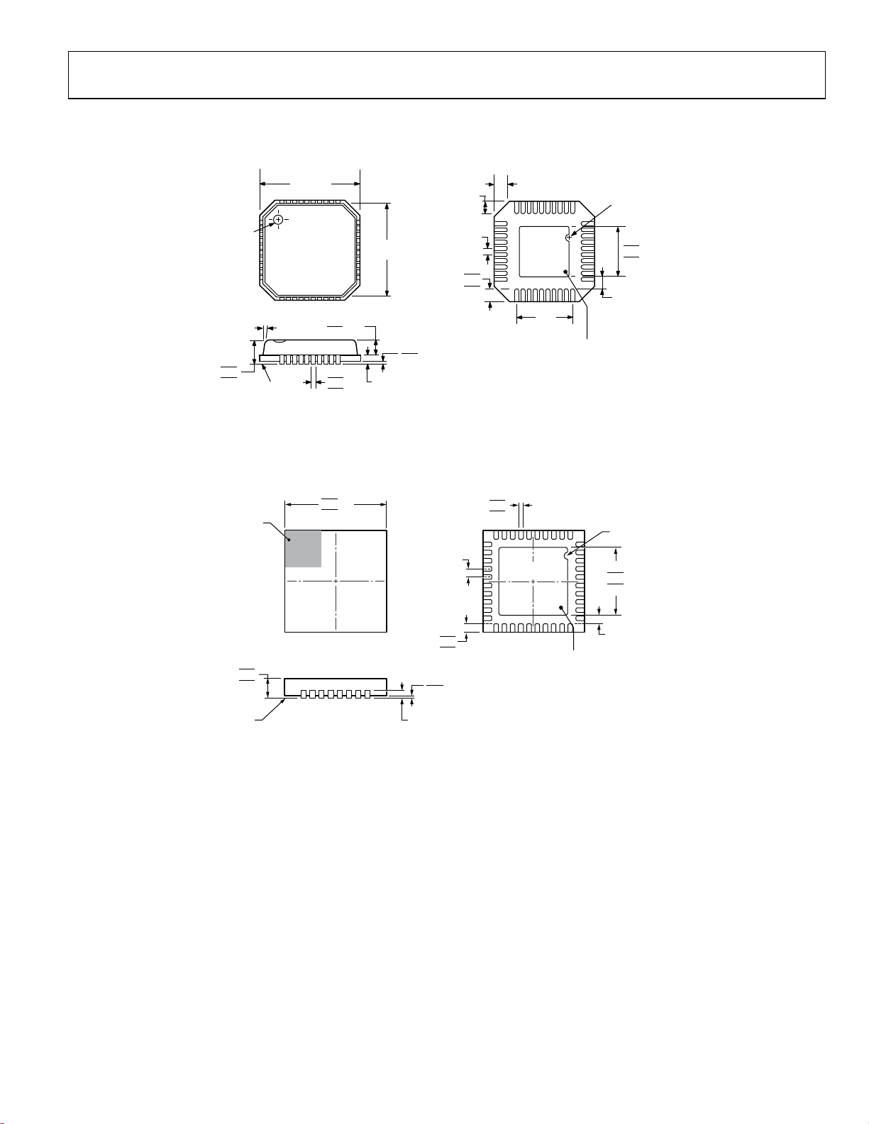
ADuC7019/20/21/22/24/25/26/27/28/29
OUTLINE DIMENSIONS
PIN 1
INDICATOR
1.00
0.85
0.80
PIN 1
INDICATOR
12° MAX
SEATING
PLANE
6.00
BSC SQ
TOP
VIEW
0.80 MAX
0.65 TYP
0.30
0.23
0.18
COMPLIANT TO JEDEC STANDARDS MO-220-VJJD-2
5.75
BSC SQ
0.20 REF
0.05 MAX
0.02 NOM
COPLANARITY
0.60 MAX
0.50
BSC
0.50
0.40
0.30
0.08
0.60 MAX
31
30
EXPOSED
PAD
(BOT TOM VIEW)
21
20
4.50
REF
FOR PROPER CONNECTION OF
THE EXPOSED PAD, REFER TO
THE PIN CONFI GURATI ON AND
FUNCTION DESCRI PTIONS
SECTION O F THIS DATA SHEET.
Figure 84. 40-Lead Lead Frame Chip Scale Package [LFCSP_VQ]
6 mm × 6 mm Body, Very Thin Quad
(CP-40-1)
Dimensions shown in millimeters
6.10
6.00 SQ
5.90
0.50
BSC
0.30
0.23
0.18
31
30
EXPOSED
PAD
PIN 1
40
10
11
1
INDICATOR
1
4.25
4.10 SQ
3.95
0.25 MIN
072108-A
N
1
P
40
I
N
I
D
4.45
4.30 SQ
4.25
R
O
C
I
A
T
0.80
0.75
0.70
SEATING
PLANE
21
0.08
20
BOTTOM VIEWTOP VIEW
0.45
0.40
0.35
0.05 MAX
0.02 NOM
COPLANARITY
0.20 REF
COMPLIANT TO JEDEC ST ANDARDS MO-220- WJJD.
10
11
0.25 MIN
FOR PROPER CONNECTION OF
THE EXPOSED PAD, REFER TO
THE PIN CONFI GURATIO N AND
FUNCTION DESCRI PTIONS
SECTION OF THIS DATA SHEET.
111808-A
Figure 85. 40-Lead Lead Frame Chip Scale Package [LFCSP_WQ]
6 mm × 6 mm Body, Very Very Thin Quad
(CP-40-10)
Dimensions shown in millimeters
Rev. D | Page 91 of 96
Page 92

ADuC7019/20/21/22/24/25/26/27/28/29
1.00
0.85
0.80
SEATING
PLANE
12° MAX
9.00
BSC SQ
PIN 1
INDICATOR
VIEW
0.60 MAX
TOP
0.80 MAX
0.65 TYP
0.50 BSC
*
COMPLIANT TO JEDEC STANDARDS MO-220-V MMD-4
EXCEPT FO R EXPOSED PAD DI MENSION
8.75
BSC SQ
0.20 REF
0.50
0.40
0.30
0.05 MAX
0.02 NOM
49
48
33
32
0.60 MAX
EXPOSED PAD
(BOTTOM VIEW)
7.50
REF
0.30
0.25
0.18
64
17
FOR PROPER CONNECTION O F
THE EXPOSE D PAD, REFER T O
THE PIN CONF IGURATIO N AND
FUNCTION DESCRIPTIO NS
SECTION OF THIS DATA SHEET.
PIN 1
INDICATOR
1
*
4.85
4.70 SQ
4.55
16
082908-B
Figure 86. 64-Lead Lead Frame Chip Scale Package [LFCSP_VQ]
9 mm x 9 mm Body, Very Thin Quad
(CP-64-1)
Dimensions shown in millimeters
12.20
PIN 1
12.00 SQ
11. 80
4964
48
0.75
0.60
0.45
1.60
MAX
1
10.20
10.00 SQ
9.80
33
32
051706-A
1.45
1.40
1.35
0.15
SEATING
0.05
PLANE
VIEW A
ROTATED 90° CCW
0.20
0.09
7°
3.5°
0°
0.08
COPLANARIT Y
COMPLIANT TO JEDEC STANDARDS MS-026-BCD
16
17
VIEW A
LEAD PITCH
0.50
BSC
TOP VIEW
(PINS DOWN)
0.27
0.22
0.17
Figure 87. 64-Lead Low Profile Quad Flat Package [LQFP]
(ST-64-2)
Dimensions shown in millimeters
Rev. D | Page 92 of 96
Page 93
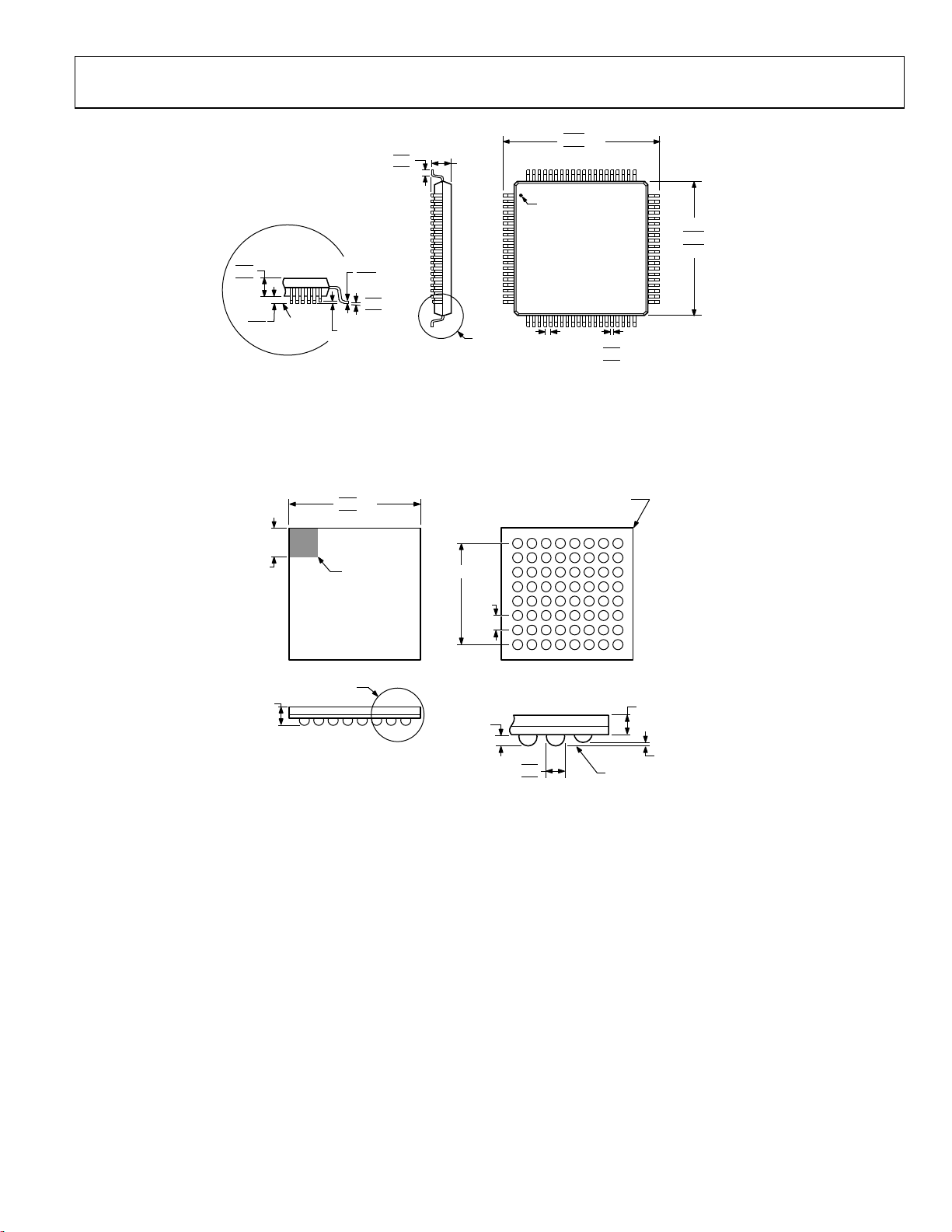
ADuC7019/20/21/22/24/25/26/27/28/29
*
1.45
1.40
1.35
0.15
SEATING
0.05
PLANE
VIEW A
ROTATED 90° CCW
0.75
0.60
0.45
0.20
0.09
7°
3.5°
0°
0.08
COPLANARIT Y
COMPLIANT TO JEDEC STANDARDS MS-026-BDD
1.60
MAX
1
20
VIEW A
PIN 1
TOP VIEW
(PINS DOWN)
21
0.50
BSC
LEAD PITCH
14.20
14.00 SQ
13.80
0.27
0.22
0.17
6180
60
12.20
12.00 SQ
11. 80
41
40
051706-A
Figure 88. 80-Lead Low Profile Quad Flat Package [LQFP]
(ST-80-1)
Dimensions shown in millimeters
1.50
SQ
1.40 MAX
6.10
6.00 SQ
5.90
BALL A1
PAD CORNER
TOP VIEW
DETAIL A
4.55 SQ
0.65
0.15 MIN
A1 CORNER
INDEX AREA
BOTTOM VI EW
DETAIL A
12345678
A
B
C
D
E
F
G
H
0.65 MIN
0.45
0.40
BALL DIAMET ER
*
COMPLIANT TO JEDEC STANDARDS MO-225
WITH THE EXCEPTIO N TO PACKAGE HEIGHT.
0.35
Figure 89. 64-Ball Chip Scale Package Ball Grid Array [CSP_BGA]
(BC-64-4)
Dimensions shown in millimeters
Rev. D | Page 93 of 96
SEATING
PLANE
COPLANARITY
0.10
030907-B
Page 94
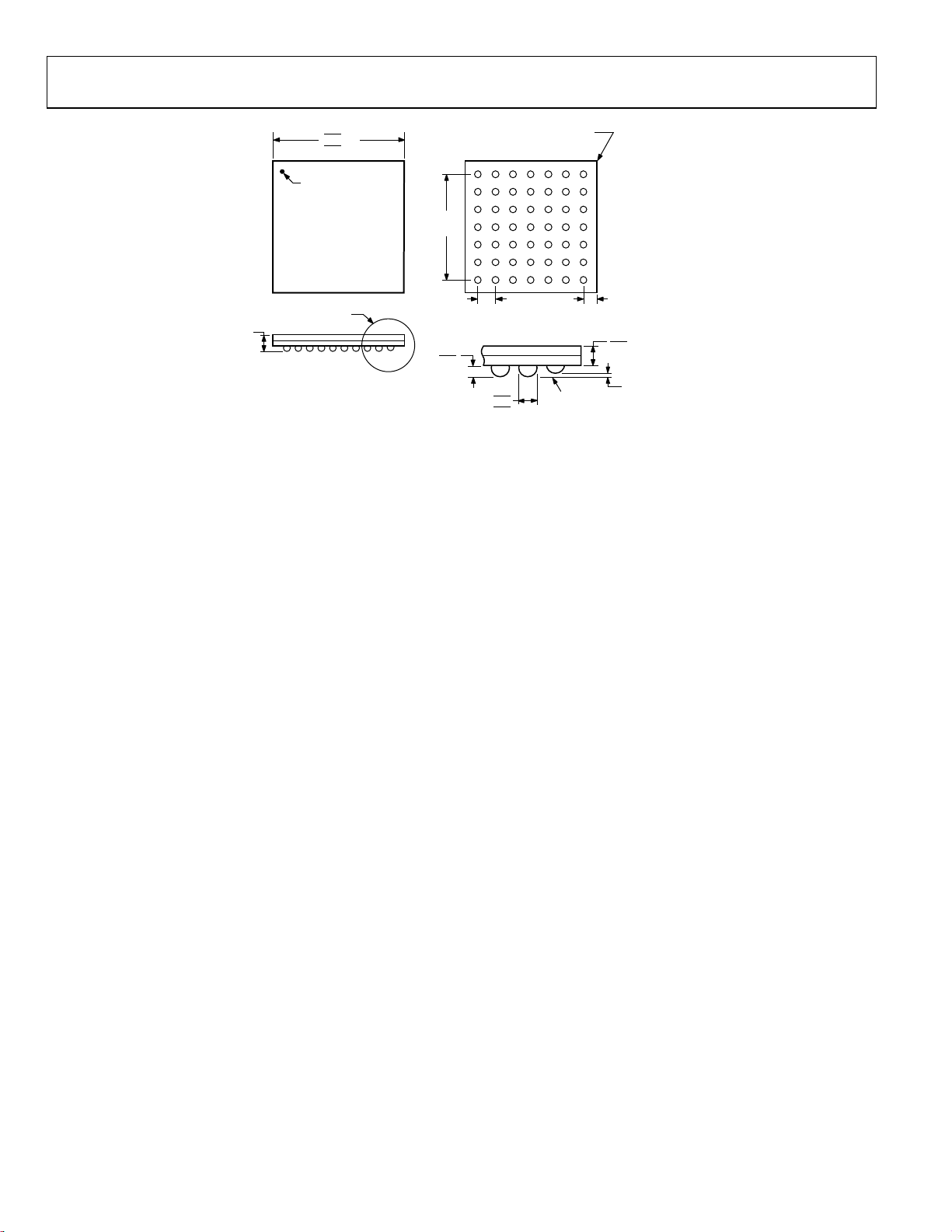
ADuC7019/20/21/22/24/25/26/27/28/29
A
R
1.20 MAX
5.05
5.00 SQ
4.95
BALL A1
INDICATOR
TOP VIEW
DETAIL A
3.90
BSC SQ
0.35
0.20
63
745
BOTTOM
0.65
VIEW
BSC
DETAIL A
0.45
0.40
0.35
BALL DIAMETER
1 CORNE
INDEX AREA
2
SEATING
PLANE
1
0.55
BSC
A
B
C
D
E
F
G
1.00 MAX
0.85 MIN
COPLANARITY
0.05 MAX
012006-0
Figure. 49-Ball Chip Scale Package Ball Grid Array [CSP_BGA]
(BC-49-1)
Dimensions shown in millimeters
Rev. D | Page 94 of 96
Page 95

ADuC7019/20/21/22/24/25/26/27/28/29
ORDERING GUIDE
1, 2
Model
ADuC7019BCPZ62I 5 3 62 kB/8 kB 14 I2C −40°C to +125°C 40-Lead LFCSP_VQ CP-40-1
ADuC7019BCPZ62I-RL 5 3 62 kB/8 kB 14 I2C −40°C to +125°C 40-Lead LFCSP_VQ CP-40-1 2,500
ADuC7019BCPZ62IRL7 5 3 62 kB/8 kB 14 I2C −40°C to +125°C 40-Lead LFCSP_VQ CP-40-1 750
ADuC7020BCPZ62 5 4 62 kB/8 kB 14 UART −40°C to +125°C 40-Lead LFCSP_VQ CP-40-1
ADuC7020BCPZ62-RL7 5 4 62 kB/8 kB 14 UART −40°C to +125°C 40-Lead LFCSP_VQ CP-40-1 750
ADuC7020BCPZ62I 5 4 62 kB/8 kB 14 I2C −40°C to +125°C 40-Lead LFCSP_VQ CP-40-1
ADuC7020BCPZ62I-RL 5 4 62 kB/8 kB 14 I2C −40°C to +125°C 40-Lead LFCSP_VQ CP-40-1 2,500
ADuC7020BCPZ62IRL7 5 4 62 kB/8 kB 14 I2C −40°C to +125°C 40-Lead LFCSP_VQ CP-40-1 750
ADuC7021BCPZ62 8 2 62 kB/8 kB 13 UART −40°C to +125°C 40-Lead LFCSP_VQ CP-40-1
ADuC7021BCPZ62-RL 8 2 62 kB/8 kB 13 UART −40°C to +125°C 40-Lead LFCSP_VQ CP-40-1 2,500
ADuC7021BCPZ62-RL7 8 2 62 kB/8 kB 13 UART −40°C to +125°C 40-Lead LFCSP_VQ CP-40-1 750
ADuC7021BCPZ62I 8 2 62 kB/8 kB 13 I2C −40°C to +125°C 40-Lead LFCSP_VQ CP-40-1
ADuC7021BCPZ62I-RL 8 2 62 kB/8 kB 13 I2C −40°C to +125°C 40-Lead LFCSP_VQ CP-40-1 2,500
ADuC7021BCPZ32 8 2 32 kB/4 kB 13 UART −40°C to +125°C 40-Lead LFCSP_VQ CP-40-1
ADuC7021BCPZ32-RL7 8 2 32 kB/4 kB 13 UART −40°C to +125°C 40-Lead LFCSP_VQ CP-40-1 750
ADuC7022BCPZ62 10 62 kB/8 kB 13 UART −40°C to +125°C 40-Lead LFCSP_VQ CP-40-1
ADuC7022BCPZ62-RL7 10 62 kB/8 kB 13 UART −40°C to +125°C 40-Lead LFCSP_VQ CP-40-1 750
ADuC7022BCPZ32 10 32 kB/4 kB 13 UART −40°C to +125°C 40-Lead LFCSP_VQ CP-40-1
ADuC7022BCPZ32-RL 10 32 kB/4 kB 13 UART −40°C to +125°C 40-Lead LFCSP_VQ CP-40-1 2,500
ADuC7024BCPZ62 10 2 62 kB/8 kB 30 UART −40°C to +125°C 64-Lead LFCSP_VQ CP-64-1
ADuC7024BCPZ62-RL7 10 2 62 kB/8 kB 30 UART −40°C to +125°C 64-Lead LFCSP_VQ CP-64-1 750
ADuC7024BCPZ62I 10 2 62 kB/8 kB 30 I2C −40°C to +125°C 64-Lead LQFP
ADuC7024BCPZ62I-RL 10 2 62 kB/8 kB 30 I2C −40°C to +125°C 64-Lead LQFP ST-64-2 2,500
ADuC7024BSTZ62 10 2 62 kB/8 kB 30 UART −40°C to +125°C 64-Lead LQFP ST-64-2
ADuC7024BSTZ62-RL 10 2 62 kB/8 kB 30 UART −40°C to +125°C 64-Lead LQFP ST-64-2 1,500
ADuC7025BCPZ62 12 62 kB/8 kB 30 UART −40°C to +125°C 64-Lead LFCSP_VQ CP-64-1
ADuC7025BCPZ62-RL 12 62 kB/8 kB 30 UART −40°C to +125°C 64-Lead LFCSP_VQ CP-64-1 2,500
ADuC7025BCPZ32 12 32 kB/4 kB 30 UART −40°C to +125°C 64-Lead LFCSP_VQ CP-64-1
ADuC7025BCPZ32-RL 12 32 kB/4 kB 30 UART −40°C to +125°C 64-Lead LFCSP_VQ CP-64-1 2,500
ADuC7025BSTZ62 12 62 kB/8 kB 30 UART −40°C to +125°C 64-Lead LQFP ST-64-2
ADuC7025BSTZ62-RL 12 62 kB/8 kB 30 UART −40°C to +125°C 64-Lead LQFP ST-64-2 1,000
ADuC7026BSTZ62 12 4 62 kB/8 kB 40 UART −40°C to +125°C 80-Lead LQFP ST-80-1
ADuC7026BSTZ62-RL 12 4 62 kB/8 kB 40 UART −40°C to +125°C 80-Lead LQFP ST-80-1 1,000
ADuC7026BSTZ62I 12 4 62 kB/8 kB 40 I2C −40°C to +125°C 80-Lead LQFP ST-80-1
ADuC7026BSTZ62I-RL 12 4 62 kB/8 kB 40 I2C −40°C to +125°C 80-Lead LQFP ST-80-1 1,000
ADuC7027BSTZ62 16 62 kB/8 kB 40 UART −40°C to +125°C 80-Lead LQFP ST-80-1
ADuC7027BSTZ62-RL 16 62 kB/8 kB 40 UART −40°C to +125°C 80-Lead LQFP ST-80-1 1,000
ADuC7027BSTZ62I 16 62 kB/8 kB 40 I2C −40°C to +125°C 80-Lead LQFP ST-80-1
ADuC7027BSTZ62I-RL 16 62 kB/8 kB 40 I2C −40°C to +125°C 80-Lead LQFP ST-80-1 1,000
ADuC7028BBCZ62 8 4 62 kB/8 kB 30 UART −40°C to +125°C 64-Ball CSP_BGA BC-64-4
ADuC7028BBCZ62-RL 8 4 62 kB/8 kB 30 UART −40°C to +125°C 64-Ball CSP_BGA BC-64-4 2,500
ADuC7029BBCZ62 7 4 62 kB/8 kB 22 UART −40°C to +125°C 49-Ball CSP_BGA BC-49-1
ADuC7029BBCZ62-RL 7 4 62 kB/8 kB 22 UART −40°C to +125°C 49-Ball CSP_BGA BC-49-1 4,000
ADuC7029BBCZ62I 7 4 62 kB/8 kB 22 I2C −40°C to +125°C 49-Ball CSP_BGA BC-49-1
ADuC7029BBCZ62I-RL 7 4 62 kB/8 kB 22 I2C −40°C to +125°C 49-Ball CSP_BGA BC-49-1 4,000
ADC
Channels3
DAC
Channels
FLASH/
RAM GPIO
Downloader
Temperature
Range
Package
Description
Package
Option
Ordering
Quantity
Rev. D | Page 95 of 96
Page 96

ADuC7019/20/21/22/24/25/26/27/28/29
1, 2
Model
EVAL-ADuC7020MKZ ADuC7020 MiniKit
EVAL-ADuC7020QSZ ADuC7020 QuickStart
EVAL-ADuC7020QSPZ ADuC7020 QuickStart
EVAL-ADuC7024QSZ ADuC7024 QuickStart
EVAL-ADuC7026QSZ ADuC7026 QuickStar
EVAL-ADuC7026QSPZ ADuC7026 QuickStart Plus
EVAL-ADuC7028QSZ ADuC7028 QuickStart
1
2
3
Z = RoHS Compliant Part.
Models ADuC7026 and ADuC7027 include an external memory interface.
One of the ADC channels is internally buffered for ADuC7019 models.
ADC
Channels
3
DAC
Channels
I2C refers to a communications protocol originally developed by Phillips Semiconductors (now NXP Semiconductors).
FLASH/
RAM
GPIO
Downloader
Temperature
Range
Package
Description
Development System
Development System
Development System
Development System
Development System
Development System
Package
Option
Ordering
Quantity
©2005-2011 Analog Devices, Inc. All rights reserved. Trademarks and
registered trademarks are the property of their respective owners.
D04955-0-5/11(D)
Rev. D | Page 96 of 96
 Loading...