

Page 1
ADTR1107-EVAL User Guide
UG-1684
22147-001
22147-002
One Technology Way • P. O . Box 9106 • Norwood, MA 02062-9106, U.S.A. • Tel : 781.329.4700 • Fax: 781.461.3113 • www.analog.com
Evaluating the ADTR1107 with 6 GHz to 18 GHz, Front-End IC
FEATURES
2-layer Rogers 4350 evaluation board with heat sink
End launch 2.9 mm RF connectors
Through calibration path (unpopulated)
EVALUATION KIT CONTENTS
2-layer, Rogers 4350, ADTR1107-EVA L evaluation board with
heat sink
EQUIPMENT NEEDED
RF signal generator
RF spectrum analyzer
RF network analyzer
5 V, 1 A power supply
3.3 V, 500 mA power supply
0 V to −2 V, 100 mA power supply
Dual supply ±3.3 V, 100 mA power supply
GENERAL DESCRIPTION
The ADTR1107-EVA L evaluation board consists of a two-layer
printed circuit board (PCB) fabricated from a 10 mil thick,
Rogers 4350B copper clad mounted to an aluminum heat sink.
The heat sink assists in providing thermal relief to the device as
well as mechanical support to the PCB. Mounting holes on the
heat sink allow attachment to larger heat sinks for improved
thermal management.
The TX_IN, ANT, RX_OUT, and CPLR_OUT ports are
populated by 2.9 mm, female coaxial connectors. The respective
RF traces of the ports have a 50 Ω characteristic impedance.
The ADTR1107-E VA L is populated with components suitable
for use over the −40°C to +85°C operating temperature range of
the ADTR1107. To calibrate board trace losses, a through
calibration path is provided. Howe ver, to use the through
calibration path, users must install and populate the path with
RF connectors.
Access to drain, ground, and gate control voltages is through
two, 24-pin headers.
RF traces are 50 Ω grounded, coplanar waveguide. Package
ground leads and the exposed paddle connect directly to the
ground plane. Multiple vias connect the top and bottom ground
planes with particular focus on the area directly beneath the
ground paddle to provide adequate electrical conduction and
thermal conduction to the heat sink.
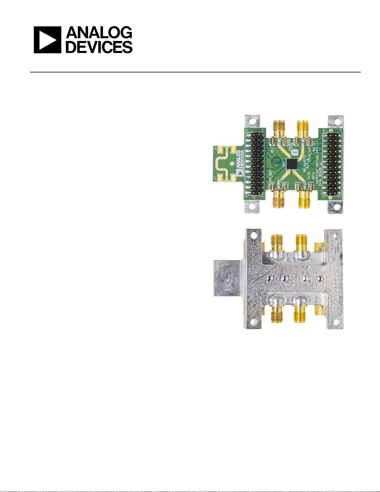
ADTR1107-EVAL PHOTOGRAPHS
igure 1. ADTR1107-EVAL Top Side
F
ure 2. ADTR1107-EVAL Bottom Side
Fig
For more information about the ADTR1107, refer to the
ADTR1107 data sheet. Consult the ADTR1107 data sheet in
conjunction with this user guide when using the ADTR1107EVA L evaluation board.
P
LEASE SEE THE LAST PAGE FOR AN IMPORTANT
WARNING AND LEGAL TERMS AND CONDITIONS.
Rev. 0 | Page 1 of 6
Page 2

UG-1684 ADTR1107-EVAL User Guide
TABLE OF CONTENTS
Features .............................................................................................. 1
Evaluation Kit Contents ................................................................... 1
Equipment Needed ........................................................................... 1
General Description ......................................................................... 1
ADTR1107-EVA L Photographs ..................................................... 1
Revision History ............................................................................... 2
Operating the ADTR1107-E VA L ................................................... 3
REVISION HISTORY
1/2020—Revision 0: Initial Version
Recommended Bias Sequences ...................................................3
Through Path Insertion Loss .......................................................4
Evaluation Board Schematic and Artwork .....................................5
Ordering Information .......................................................................6
Bill of Materials ..............................................................................6
Rev. 0 | Page 2 of 6
Page 3

ADTR1107-EVAL User Guide UG-1684
OPERATING THE ADTR1107-EVAL
A 5 V, 1 A power supply is required to provide the bias to the
power amplifier in the transmit path. The 5 V power supply is
connected through Pin 10 of the J6 header. Addi tion a l ly, a 0 V to
−2 V, 100 mA power supply is required to provide the required
gate control voltage. The gate control voltage is supplied
through Pin 6 of the J6 header.
A 3.3 V, 100 mA power supply is required to provide the bias to
the low noise amplifier (LNA) in the receive path. The 3.3 V
supply is connected to the VGG_LNA pin through Pin 6 of the
J5 header.
The dual ±3.3 V, 100 mA supply is required to provide the bias
to the switch. The 3.3 V supply connects to the VDD_SW pin
through Pin 22 of the J5 header. The −3.3 V supply connects to
the VSS_SW pin through Pin 18 of the J5 header.
Control the state of the switch by applying the proper logic level
to Pin 20 of the J5 header, as defined in the Table 1.
Use the biasing sequences described in the Transmit State
Power-Up section, the Transmit State Power-Down section, the
Receive State Power-Up section, and the Receive State PowerDown section when powering up and powering down. Refer to
Tabl e 2 for the ADTR1107 pin connections through the header
connector.
Table 1. Switch Logic Truth Table
Signal Path State
Control Input (V
Low On Off
High Off On
) State TX_IN to ANT ANT to RX_OUT
CTRL
RECOMMENDED BIAS SEQUENCES
Transmit State Power-Up
The recommended bias sequence during the transmit state
power-up is as follows:
1. Connect all GND pins to ground.
2. Set the VDD_SW pin to 3.3 V.
3. Set the VSS_SW pin to −3.3 V.
4. Set the CTRL_SW pin to 0 V.
5. Set the VGG_LNA pin t o 0 V.
6. Set the VDD_LNA pin to 0 V.
7. Set the VGG_PA pin to −1.75 V.
8. Set the VDD_PA pin to 5 V.
9. Increase the VGG_PA pin voltage to achieve the desired
quiescent current (I
10. Apply the RF signal to the TX_IN pin.
_PA) of t h e power amplifier.
DQ
Transmit State Power-Down
The recommended transmit state bias sequence during
power-down is as follows:
1. Tu rn off the RF signal.
2. Decrease the VGG_PA pin voltage to −1.75 V.
3. Set the V D D _ PA pin to 0 V.
4. Set the VSS_SW to 0 V.
5. Set the VDD_SW to 0 V.
Receive State Power-Up
The recommended bias sequence during the receive state
power-up is as follows:
1. Connect all GND pins to ground.
2. Set the VDD_SW pin to 3.3 V.
3. Set the VSS_SW pin to −3.3 V.
4. Set the CTRL_SW pin to 3.3 V.
5. Set the VGG_PA pin to −1.75 V.
6. Set the VDD_PA pin to 0 V.
7. Set the VGG_ L NA pi n t o 0 V.
8. Set the VDD_LNA pin to 3.3 V.
9. Apply the RF signal to the ANT pin.
Receive State Power-Down
The recommended receive state bias sequence during
power-down is as follows:
1. Turn off the RF signal.
2. Set the V D D _ PA pin to 0 V.
3. Set the VGG_PA pin to 0 V.
4. Set the CTRL_SW pin to 0 V.
5. Set the VSS_SW pin to 0 V.
6. Set the VDD_SW pin to 0 V.
Table 2. J5 and J6 Header Connections to the ADTR1107
Connector Header ADTR1107 Pin
J5 1 to 5, 7 to 9, 11 to 17, 19, 21,
23, 24
6 VDD_LNA
10 VGG_LNA
18 VSS_SW
20 CTRL_SW
22 VDD_SW
J6 1 to 5, 7 to 9, 11 to 24 GND
6 VGG_PA
10 VDD_PA
GND
Rev. 0 | Page 3 of 6
Page 4

UG-1684 ADTR1107-EVAL User Guide
0
–40
–35
–30
–25
–20
–15
–10
–5
6 8 10 12 14 16 18
INSERTION LOSS AND RETURN LOSS (dB)
FREQUENCY (GHz)
22147-005
OUTPUT RETURN LOSS
INSERTION LOSS
INPUT RETURN LOSS
THROUGH PATH INSERTION LOSS
Figure 3 shows the data plot in Tabl e 3 of the through
calibration path (J7 to J8).
gure 3. Insertion Loss and Return Loss (Input and Output) of the Through
Fi
Calibration Path
Table 3. Insertion Loss and Input and Output Return Loss of
the Through Calibration Path
Frequency (GHz) Insertion Loss (dB)
6 −0.5
6.5 −0.5
8 −0.6
8.5 −0.7
10 −0.8
10.5 −0.8
12 −0.9
12.5 −0.9
14 −1.1
14.5 −1.1
16 −1.1
16.5 −1.2
18 −1.4
Rev. 0 | Page 4 of 6
Page 5

ADTR1107-EVAL User Guide UG-1684
21
9
7
231019
8
24
5
2
17
EPAD
22
18
16
15
14
13
11
6
4
3
1
20
12
R1
ANT
TX_IN
24
22
20
18
16
14
12
10
8
6
4
2
23
21
19
17
15
13
11
9
7
5
3
1
J5
23
21
19
17
13
11
9
7
5
3
1
24
22
20
18
16 15
14
12
10
8
6
4
2
J6
VDD_LNA
VDD_PA
VGG_PA
VGG_LNA
VSS_SW
CTRL_SW
VDD_SW
GND
GND
GND
GND
GND
TX_IN
RX_OUT
GND
GND
GND
GND
GND
ANT
EPAD
VGG_LNA
GND
CTRL_SW
VSS_SW
VDD_SW
VDD_LNA
VDD_PA
NIC
GND
NIC
CPLR_OUT
VGG_PA
GND
ADTR1107
J7
J8
DNI DNI
DNI
CPLR_OUT
RX_OUT
U1
GND
GND GND
R2
DNI
22147-003
22147-004
GND
GND
GND
GND
GND
GND
GND
GND
GND
GND
1
GND
GND
GND
GND
GNDGND
GND
GND
GND
GND
GND
GND
GND
GND
GND
GND
GND
GND
GND
GND
GND
1
VDDLNA
VGGLNA
VSSSW
VDDSW
CTRLSW
VGGPA
VDDPA
GND
GND
GND
GND
GND
GND
GND
NC
NC
NC
EVALUATION BOARD SCHEMATIC AND ARTWORK
ure 4. ADTR1107-EVAL Evaluation Board Schematic
Fig
re 5. ADTR1107-EVAL Assembly Drawing (J7, J8, R1, and R2 Not Installed)
Figu
Rev. 0 | Page 5 of 6
Page 6

UG-1684 ADTR1107-EVAL User Guide
ORDERING INFORMATION
BILL OF MATERIALS
Table 4.
Reference Designator Description Manufacturer Part Number
TX_IN, RX_OUT, ANT, CLPR_OUT Connectors, Type K, jack edge Winchester Connector 25-146-1000-92
J7, J8 Connectors, Type K, jack edge, do not install (DNI) Winchester Connector 25-146-1000-92
J5 and J6
PCB connector headers, 24-position male headers,
unshrouded double row, surface-mount (SMT), 2.54 mm pitch
R1 and R2 Thick film resistor chip. DNI Not applicable Not applicable
U1 IC, transmit/receive module Analog Devices, Inc. ADTR1107ACCZ
Not Applicable 2.51 inch × 1.9 inch heat sink Not applicable Not applicable
Samtec, Inc. TSM-112-01-L-DV
ESD Caution
ESD (electrostatic discharge) sensitive device. Charged devices and circuit boards can discharge without detection. Although this product features patented or proprietary protection
circuitry, damage may occur on devices subjected to high energy ESD. Therefore, proper ESD precautions should be taken to avoid performance degradation or loss of functionality.
Legal Terms and Conditions
By using the evaluation board discussed herein (together with any tools, components documentation or support materials, the “Evaluation Board”), you are agreeing to be bound by the terms and conditions
set forth below (“Agreement”) unless you have purchased the Evaluation Board, in which case the Analog Devices Standard Terms and Conditions of Sale shall govern. Do not use the Evaluation Board until you
have read and agreed to the Agreement. Your use of the Evaluation Board shall signify your acceptance of the Agreement. This Agreement is made by and between you (“Customer”) and Analog Devices, Inc.
(“ADI”), with its principal place of business at One Technology Way, Norwood, MA 02062, USA. Subject to the terms and conditions of the Agreement, ADI hereby grants to Customer a free, limited, personal,
temporary, non-exclusive, non-sublicensable, non-transferable license to use the Evaluation Board FOR EVALUATION PURPOSES ONLY. Customer understands and agrees that the Evaluation Board is provided
for the sole and exclusive purpose referenced above, and agrees not to use the Evaluation Board for any other purpose. Furthermore, the license granted is expressly made subject to the following additional
limitations: Customer shall not (i) rent, lease, display, sell, transfer, assign, sublicense, or distribute the Evaluation Board; and (ii) permit any Third Party to access the Evaluation Board. As used herein, the term
“Third Party” includes any entity other than ADI, Customer, their employees, affiliates and in-house consultants. The Evaluation Board is NOT sold to Customer; all rights not expressly granted herein, including
ownership of the Evaluation Board, are reserved by ADI. CONFIDENTIALITY. This Agreement and the Evaluation Board shall all be considered the confidential and proprietary information of ADI. Customer may
not disclose or transfer any portion of the Evaluation Board to any other party for any reason. Upon discontinuation of use of the Evaluation Board or termination of this Agreement, Customer agrees to
promptly return the Evaluation Board to ADI. ADDITIONAL RESTRICTIONS. Customer may not disassemble, decompile or reverse engineer chips on the Evaluation Board. Customer shall inform ADI of any
occurred damages or any modifications or alterations it makes to the Evaluation Board, including but not limited to soldering or any other activity that affects the material content of the Evaluation Board.
Modifications to the Evaluation Board must comply with applicable law, including but not limited to the RoHS Directive. TERMINATION. ADI may terminate this Agreement at any time upon giving written
notice to Customer. Customer agrees to return to ADI the Evaluation Board at that time. LIMITATION OF LIABILITY. THE EVALUATION BOARD PROVIDED HEREUNDER IS PROVIDED “AS IS” AND ADI MAKES NO
WARRANTIES OR REPRESENTATIONS OF ANY KIND WITH RESPECT TO IT. ADI SPECIFICALLY DISCLAIMS ANY REPRESENTATIONS, ENDORSEMENTS, GUARANTEES, OR WARRANTIES, EXPRESS OR IMPLIED,
RELATED TO THE EVALUATION BOARD INCLUDING, BUT NOT LIMITED TO, THE IMPLIED WARRANTY OF MERCHANTABILITY, TITLE, FITNESS FOR A PARTICULAR PURPOSE OR NONINFRINGEMENT OF
INTELLECTUAL PROPERTY RIGHTS. IN NO EVENT WILL ADI AND ITS LICENSORS BE LIABLE FOR ANY INCIDENTAL, SPECIAL, INDIRECT, OR CONSEQUENTIAL DAMAGES RESULTING FROM CUSTOMER’S
POSSESSION OR USE OF THE EVALUATION BOARD, INCLUDING BUT NOT LIMITED TO LOST PROFITS, DELAY COSTS, LABOR COSTS OR LOSS OF GOODWILL. ADI’S TOTAL LIABILITY FROM ANY AND ALL CAUSES
SHALL BE LIMITED TO THE AMOUNT OF ONE HUNDRED US DOLLARS ($100.00). EXPORT. Customer agrees that it will not directly or indirectly export the Evaluation Board to another country, and that it will
comply with all applicable United States federal laws and regulations relating to exports. GOVERNING LAW. This Agreement shall be governed by and construed in accordance with the substantive laws of the
Commonwealth of Massachusetts (excluding conflict of law rules). Any legal action regarding this Agreement will be heard in the state or federal courts having jurisdiction in Suffolk County, Massachusetts, and
Customer hereby submits to the personal jurisdiction and venue of such courts. The United Nations Convention on Contracts for the International Sale of Goods shall not apply to this Agreement and is
expressly disclaimed.
©2020 Analog Devices, Inc. All rights reserved. Trademarks and
registered trademarks are the property of their respective owners.
UG22147-0-1/20(0)
Rev. 0 | Page 6 of 6
 Loading...