
SPI/I2C Compatible, Temperature Sensor,
4-Channel ADC and Quad Voltage Output DAC
FEATURES
ADT7516—four 12-bit DACs
ADT7517—four 10-bit DACs
ADT7519—four 8-bit DACs
Buffered voltage output
Guaranteed monotonic by design over all codes
10-bit temperature-to-digital converter
10-bit 4-channel ADC
DC input bandwidth
Input range: 0 V to 2.28 V
Temperature range: –40°C to +120°C
Temperature sensor accuracy of typ: ±0.5°C
Supply range: 2.7 V to 5.5 V
DAC output range: 0 V to 2 V
Power-down current: 1 µA
Internal 2.28 V
option
REF
Double-buffered input logic
Buffered reference input
Power-on reset to 0 V DAC output
Simultaneous update of outputs (
On-chip rail-to-rail output buffer amplifier
®
, I2C®, QSPI™, MICROWIRE™, and DSP compatible
SPI
4-wire serial interface
SMBus packet error checking (PEC) compatible
16-lead QSOP package
GENERAL DESCRIPTION
The ADT7516/ADT7517/ADT75191 combine a 10-bit temperature-to-digital converter, a 10-bit 4-channel ADC, and a
quad 12-/10-/8-bit DAC, respectively, in a 16-lead QSOP
package. The parts also include a band gap temperature sensor
and a 10-bit ADC to monitor and digitize the temperature
reading to a resolution of 0.25°C.
The ADT7516/ADT7517/ ADT7519 operate from a single 2.7 V
to 5.5 V supply. The input voltage range on the ADC channels is
0 V to 2.28 V, and the input bandwidth is dc. The reference for
the ADC channels is derived internally. The output voltage of
the DAC ranges from 0 V to V
time of 7 ms typical.
The ADT7516/ADT7517/ADT7519 provide two serial interface
options: a 4-wire serial interface that is compatible with SPI,
QSPI, MICROWIRE, and DSP interface standards, and a 2-wire
Rev. A
Information furnished by Analog Devices is believed to be accurate and reliable.
However, no responsibility is assumed by Analog Devices for its use, nor for any
infringements of patents or other rights of third parties that may result from its use.
Specifications subject to change without notice. No license is granted by implication
or otherwise under any patent or patent rights of Analog Devices. Trademarks and
registered trademarks are the property of their respective owners.
REF
function)
LDAC
, with an output voltage settling
DD
ADT7516/ADT7517/ADT7519
APPLICATIONS
Portable battery-powered instruments
Personal computers
Smart battery chargers
Telecommunications systems
Electronic text equipment
Domestic appliances
Process control
PIN CONFIGURATION
V
-B
1
OUT
V
-A
2
OUT
V
REF
D+/AIN1
D–/AIN2
GND
V
-IN
CS
DD
ADT7516/
3
ADT7517/
ADT7519
4
TOP VIEW
5
(Not to Scale)
6
7
8
Figure 1.
2
SMBus/I
C interface. They feature a standby mode that is
controlled through the serial interface.
The reference for the four DACs is derived either internally or
from a reference pin. The outputs of all DACs may be updated
simultaneously using the software LDAC function or the
LDAC
external
pin. The ADT7516/ADT7517/ADT7519
incorporate a power-on reset circuit, which ensures that the
DAC output powers up to 0 V and remains there until a valid
write takes place.
The ADT7516/ADT7517/ADT7519’s wide supply voltage range,
low supply current, and SPI/I
2
them ideal for a variety of applications, including personal
computers, office equipment, and domestic appliances.
1
Protected by the following U.S. Patent Numbers: 6,169,442; 5,867,012;
5,764174. Other patents pending.
One Technology Way, P.O. Box 9106, Norwood, MA 02062-9106, U.S.A.
Tel: 781.329.4700
Fax: 781.326.8703 © 2004 Analog Devices, Inc. All rights reserved.
www.analog.com
V
-C
16
OUT
V
-D
15
OUT
14
AIN4
13
SCL/SCLK
12
SDA/DIN
11
DOUT/ADD
10
INT/INT
9
LDAC/AIN3
C compatible interface make
02883-A-006

ADT7516/ADT7517/ADT7519
TABLE OF CONTENTS
Specifications..................................................................................... 3
Conversion Speed....................................................................... 19
DAC AC Characteristics .............................................................. 6
Functional Block Diagram .............................................................. 8
Absolute Maximum Ratings............................................................ 9
ESD Caution.................................................................................. 9
Pin Configuration and Functional Descriptions........................ 10
Te r m in o l o g y .................................................................................... 11
Typical Performance Characteristics ........................................... 13
Theory of Operation ...................................................................... 19
Power-Up Calibration ................................................................ 19
REVISION HISTORY
8/04—Data Sheet Changed from Rev. 0 to Rev. A
Updated Format...................................................................... Universal
Deleted ADT7518
Added ADT7519..................................................................... Universal
Change to Internal V
Change to Equation.............................................................................26
Value ..............................................................5
REF
Function Description—Voltage Output.................................. 20
Functional Description—Analog Inputs................................. 23
ADC Transfer Function............................................................. 23
Functional Description—Measurement.................................. 25
ADT7516/ADT7517/ADT7519 Registers............................... 28
Serial Interface............................................................................ 37
SMBus Alert Response............................................................... 43
Outline Dimensions....................................................................... 44
Ordering Guide .......................................................................... 44
7/03—Initial Version: Rev. 0
Rev. A | Page 2 of 44

ADT7516/ADT7517/ADT7519
SPECIFICATIONS
Table 1. Temperature range is as follows: A version: –40°C to +120°C. VDD = 2.7 V to 5.5 V, GND = 0 V, REFIN = 2.25 V, unless
otherwise noted.
Parameter
DAC DC PERFORMANCE
ADT7519
ADT7517
ADT7516
ADC DC ACCURACY Max VDD = 5 V.
Resolution 10 Bits
Total Unadjusted Error (TUE) 2 3 % of FSR
Offset Error ±0.5 % of FSR
Gain Error ±2 % of FSR
ADC BANDWIDTH DC Hz
ANALOG INPUTS
Input Voltage Range 0 2.28 V AIN1 to AIN4. C4 = 0 in Control Configuration 3.
0 V
DC Leakage Current ±1 µA
Input Capacitance 5 20 pF
Input Resistance 10 MΩ
THERMAL CHARACTERISTICS
INTERNAL TEMPERATURE SENSOR
Accuracy @ VDD = 3.3 V ±10% ±1.5 °C TA = 85°C.
±0.5 ±3 °C TA = 0°C to +85°C.
±2 ±5 °C TA = –40°C to +120°C.
Accuracy @ VDD = 5 V ±5% ±2 ±3 °C TA = 0°C to +85°C.
±3 ±5 °C TA = –40°C to +120°C.
Resolution 10 Bits Equivalent to 0.25°C.
Long-Term Drift 0.25 °C Drift over 10 years if part is operated at 55°C.
1
2, 3
Min Typ Max Unit Conditions/Comments
Resolution 8 Bits
Relative Accuracy ±0.15 ±1 LSB
Differential Nonlinearity ±0.02 ±0.25 LSB Guaranteed monotonic over all codes.
Resolution 10 Bits
Relative Accuracy ±0.5 ±4 LSB
Differential Nonlinearity ±0.05 ±0.5 LSB Guaranteed monotonic over all codes.
Resolution 12 Bits
Relative Accuracy ±2 ±16 LSB
Differential Nonlinearity ±0.02 ±0.9 LSB Guaranteed monotonic over all codes.
Offset Error ±0.4 ±2 % of FSR
Gain Error ±0.3 ±2 % of FSR
Lower Deadband 20 65 mV
Lower deadband exists only if offset error is
negative. See Figure 8.
Upper Deadband 60 100 mV
Upper deadband exists if V
= VDD and off-set
REF
plus gain error is positive. See Figure 9.
Offset Error Drift
4
–12 ppm of FSR/°C
Gain Error Drift4 –5 ppm of FSR/°C
DC Power Supply Rejection
4
Ratio
–60 dB ∆V
= ±10%.
DD
DC Crosstalk4 200 µV See Figure 5.
DD
V AIN1 to AIN4. C4 = 0 in Control Configuration 3.
Internal reference used. Averaging on.
Rev. A | Page 3 of 44

ADT7516/ADT7517/ADT7519
Parameter
THERMAL CHARACTERISTICS
1
Min Typ Max Unit Conditions/Comments
External transistor = 2N3906.
EXTERNAL TEMPERATURE SENSOR
Accuracy @ VDD = 3.3 V ±10% ±1.5 °C TA = 85°C.
±3 °C T
±5 °C T
= 0°C +85°C.
A
= –40°C to +120°C.
A
Accuracy @ VDD = 5 V ±5% ±2 ±3 °C TA = 0°C +85°C.
±3 ±5 °C TA = –40°C to +120°C.
Resolution 10 Bits Equivalent to 0.25°C.
Output Source Current 180 µA High Level.
11 µA Low Level.
Thermal Voltage Output
8-Bit DAC Output
Resolution 1 °C
Scale Factor 8.97 mV/°C 0 V to V
17.58 mV/°C 0 V to 2 V
output. TA = –40°C to +120°C.
REF
output. TA = –40°C to +120°C.
REF
10-Bit DAC Output
Resolution 0.25 °C
Scale Factor 2.2 mV/°C 0 V to V
4.39 mV/°C 0 V to 2 V
output. TA = –40°C to +120°C.
REF
output. TA = –40°C to +120°C.
REF
CONVERSION TIMES Single channel mode.
Slow ADC
VDD/AIN 11.4 ms Averaging (16 samples) on.
712 µs Averaging off.
Internal Temperature 11.4 ms Averaging (16 samples) on.
712 µs Averaging off.
External Temperature 24.22 ms Averaging (16 samples) on.
1.51 ms Averaging off.
Fast ADC
VDD/AIN 712 µs Averaging (16 samples) on.
44.5 µs Averaging off.
Internal Temperature 2.14 ms Averaging (16 samples) on.
134 µs Averaging off.
External Temperature 14.25 ms Averaging (16 samples) on.
890 µs Averaging off.
ROUND ROBIN UPDATE RATE
Slow ADC @ 25°C
5
Time to complete one measurement cycle
through all channels.
Averaging On 79.8 ms AIN1 and AIN2 are selected on Pins 7 and 8.
Averaging Off 4.99 ms AIN1 and AIN2 are selected on Pins 7 and 8.
Averaging On 94.76 ms D+ and D– are selected on Pins 7 and 8.
Averaging Off 9.26 ms D+ and D-– are selected on Pins 7 and 8.
Fast ADC @ 25°C
Averaging On 6.41 ms AIN1 and AIN2 are selected on Pins 7 and 8.
Averaging Off 400.84 µs AIN1 and AIN2 are selected on Pins 7 and 8.
Averaging On 21.77 ms D+ and D– are selected on Pins 7 and 8.
Averaging Off 3.07 ms D+ and D– are selected on Pins 7 and 8.
DAC EXTERNAL REFERENCE INPUT4
V
Input Range 1 V
REF
V
Input Impedance >10 MΩ Buffered reference and power-down mode.
REF
DD
V Buffered reference.
Reference Feedthrough –90 dB Frequency = 10 kHz.
Channel-to-Channel Isolation –75 dB Frequency = 10 kHz.
Rev. A | Page 4 of 44

ADT7516/ADT7517/ADT7519
Parameter
1
Min Typ Max Unit Conditions/Comments
ON-CHIP REFERENCE
Reference Voltage4 2.28 V
Temperature Coefficient4 80 ppm/°C
OUTPUT CHARACTERISTICS4
Output Voltage
6
0.001 VDD − 0.1 V
This is a measure of the minimum and maximum
drive capability of the output amplifier.
DC Output Impedance 0.5 Ω
Short Circuit Current 25 mA VDD = 5 V.
16 mA VDD = 3 V.
Power-Up Time 2.5 µs Coming out of power-down mode. VDD = 5 V.
5 µs Coming out of power-down mode. VDD = 3.3 V.
DIGITAL INPUTS4
Input Current ±1 µA VIN = 0 V to V
DD.
VIL, Input Low Voltage 0.8 V
VIH, Input High Voltage 1.89 V
Pin Capacitance 3 10 pF All digital inputs.
SCL, SDA Glitch Rejection 50 ns
Input filtering suppresses noise spikes of less
than 50 ns.
LDAC Pulse Width
20 ns Edge triggered input.
DIGITAL OUTPUT
Digital High Voltage, V
Output Low Voltage, V
Output High Current, I
Output Capacitance, C
OH
OL
OH
OUT
INT/INT Output Saturation Voltage
I2C TIMING CHARACTERISTICS 7,
Serial Clock Period, t
1
8
2.4 V I
SOURCE
= I
= 200 µA.
SINK
0.4 V IOL = 3 mA.
1 mA V
= 5 V.
OH
50 pF
0.8 V I
= 4 mA.
OUT
2.5 µs Fast Mode I2C. See Figure 2.
Data In Setup Time to SCL High, t250 ns
Data Out Stable after SCL Low, t
SDA Low Setup Time to SCL
Low (Start Condition), t
4
SDA High Hold Time after SCL
High (Stop Condition), t
SDA and SCL Fall Time, t
5
6
SPI TIMING CHARACTERISTICS
CS to SCLK Setup Time, t
SCLK High Pulse Width, t
SCLK Low Pulse Width, t
Data Access Time after SCLK
Falling Edge, t
10
,
4
1
2
3
Data Setup Time Prior to SCLK
Rising Edge, t
5
Data Hold Time after SCLK Rising
Edge, t
6
CS to SCLK Hold Time, t
7
CS to DOUT High Impedance, t
, 9
4
0 ns See Figure 2.
3
50 ns See Figure 2.
50 ns See Figure 2.
90 ns See Figure 2.
0 ns See Figure 3.
50 ns See Figure 3.
50 ns See Figure 3.
35 ns
20 ns See Figure 3.
0 ns See Figure 3.
0 µs See Figure 3.
40 ns See Figure 3.
8
Rev. A | Page 5 of 44
ADT7516/ADT7517/ADT7519
T
Parameter
1
Min Typ Max Unit Conditions/Comments
POWER REQUIREMENTS
V
DD
2.7 5.5 V
VDD Settling Time 50 ms VDD settles to within 10% of its final voltage level.
IDD (Normal Mode)
11
3 mA V
= 3.3 V, VIH = VDD, and VIL = GND.
DD
2.2 3 mA VDD = 5 V, VIH = VDD, and VIL = GND.
IDD (Power-Down Mode) 10 µA VDD = 3.3 V, VIH = VDD, and VIL = GND.
10 µA VDD = 5 V, VIH = VDD, and VIL = GND.
Power Dissipation 10 mW VDD = 3.3 V. Normal mode.
33 µW VDD = 3.3 V. Shutdown mode.
1
See the section. Terminology
2
DC specifications are tested with the outputs unloaded.
3
Linearity is tested using a reduced code range: ADT7516 (Code 115 to 4095); ADT7517 (Code 28 to 1023); ADT7519 (Code 8 to 255).
4
Guaranteed by design and characterization, not production tested.
5
Round robin is the continuous sequential measurement of the following channels: VDD, internal temperature, external temperature (AIN1, AIN2), AIN3, and AIN4.
6
For the amplifier output to reach its minimum voltage, the offset error must be negative. For the amplifier output to reach its maximum voltage (V
plus gain error must be positive.
7
The SDA and SCL timing is measured with the input filters turned on to meet the fast-mode I2C specification. Switching off the input filters improves the transfer rate
but has a negative effect on the EMC behavior of the part.
8
Guaranteed by design, not production tested.
9
All input signals are specified with tr = tf = 5 ns (10% to 90% of VDD), and timed from a voltage level of 1.6 V.
10
Measured with the load circuit shown in Figure 4.
11
The IDD specification is valid for all DAC codes and full-scale analog input voltages. Interface inactive. All DACs and ADCs active. Load currents excluded.
= VDD), the offset
REF
DAC AC CHARACTERISTICS
Table 2. VDD = 2.7 V to 5.5 V, RL = 4.7 kΩ to GND; CL = 200 pF to GND; 4.7 kΩ to VDD; all specifications T
otherwise noted.
Parameter
1, 2
Min Typ
Output Voltage Settling Time V
3
Max Unit Conditions/Comments
= VDD = 5 V.
REF
ADT7519 6 8 µs 1/4 scale to 3/4 scale change (40h to C0h).
ADT7517 7 9 µs 1/4 scale to 3/4 scale change (100h to 300h).
ADT7516 8 10 µs 1/4 scale to 3/4 scale change (400h to C00h).
Slew Rate 0.7 V/µs
Major-Code Change Glitch Energy 12 nV-s 1 LSB change around major carry.
Digital Feedthrough 0.5 nV-s
Digital Crosstalk 1 nV-s
Analog Crosstalk 0.5 nV-s
DAC-to-DAC Crosstalk 3 nV-s
Multiplying Bandwidth 200 kHz V
Total Harmonic Distortion –70 dB V
= 2 V ±0.1 V p-p.
REF
= 2.5 V ±0.1 V p-p. Frequency = 10 kHz.
REF
1
See section. Terminology
2
Guaranteed by design and characterization, not production tested.
3
@ 25°C.
SCL
SDA
DATA IN
SDA
DATA OU
t
4
t
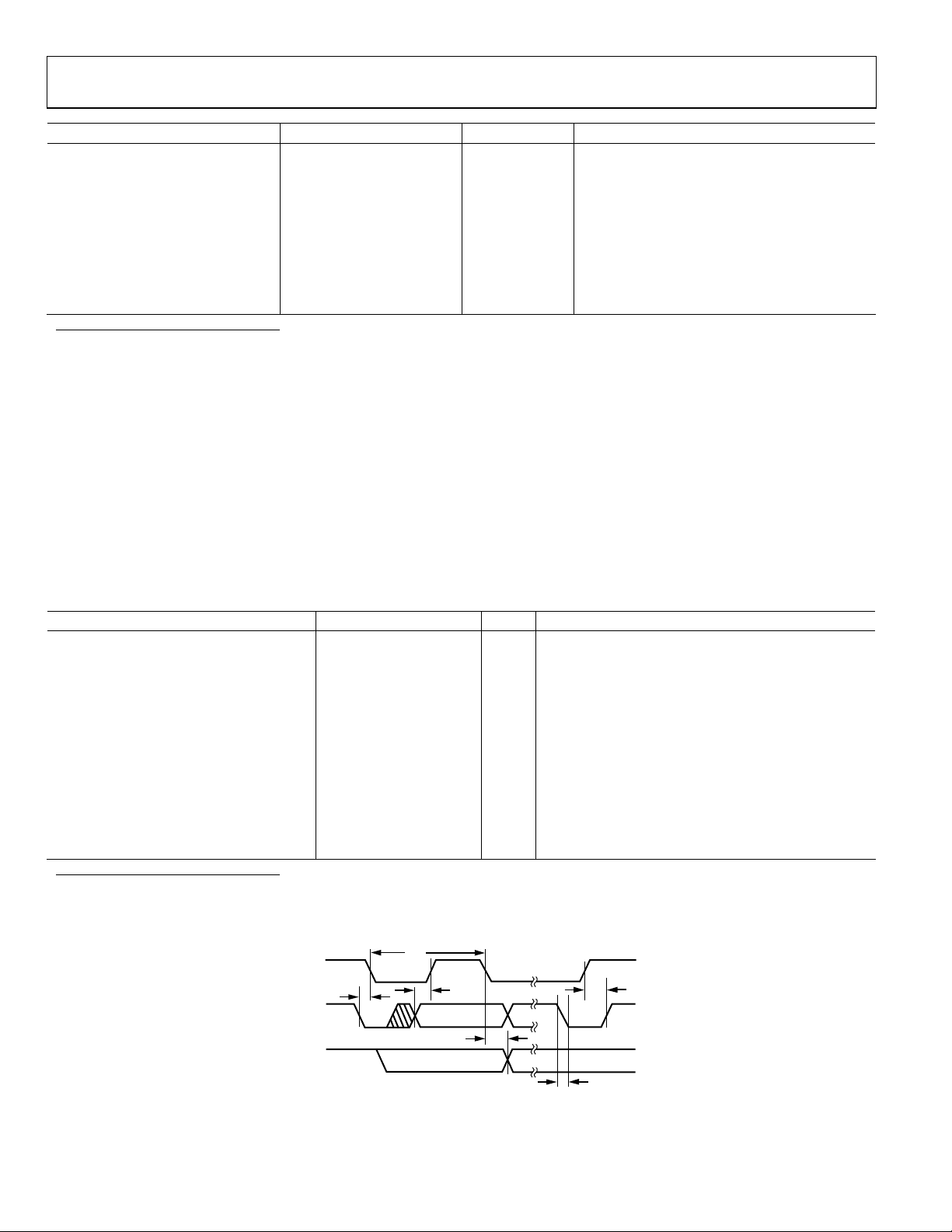
Figure 2. I
1
t
2
t
3
2
C Bus Timing Diagram
t
5
t
6
02883-A-002
MIN
to T
MAX
, unless
Rev. A | Page 6 of 44
ADT7516/ADT7517/ADT7519
O
CS
t
1
SCLK
DIN
DOUT
D7
XXXXXXXXD7D6D5D4D3D2D1 D0
t
2
t
t
3
D6 D5 D4 D3 D2 D1 D0 X X X X X X X X
t
6
5
t
4
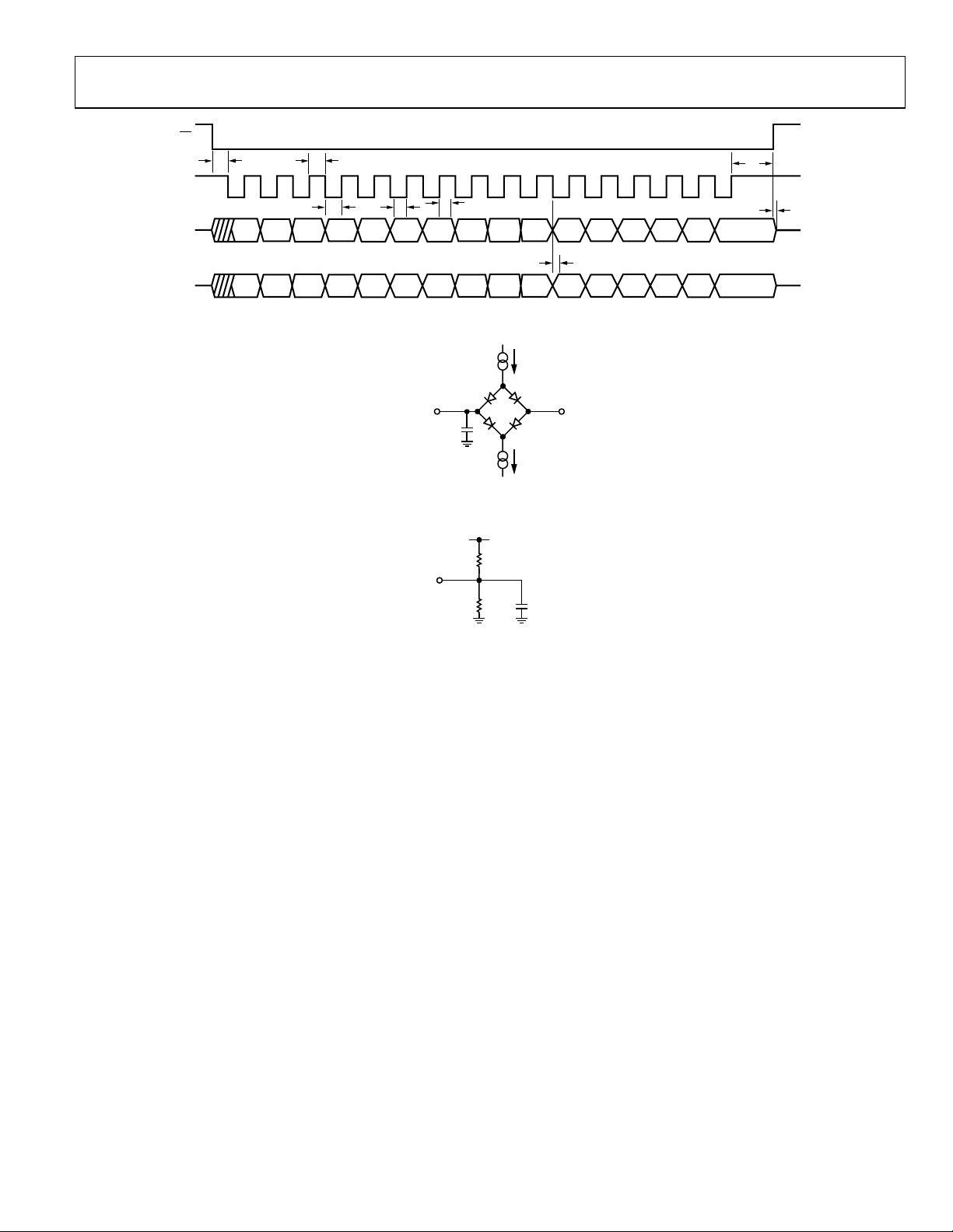
Figure 3. SPI Bus Timing Diagram
t
7
t
8
02883-A-003
200µAI
TO OUTPUT
PIN
C
L
50pF
200µAI
Figure 4. Load Circuit for Access Time and Bus Relinquish Time
OL
1.6V
OH
02883-A-004
V
DD
TO DAC
UTPUT
Figure 5. Load Circuit for DAC Outputs
4.7kΩ
4.7kΩ
200pF
02883-A-005
Rev. A | Page 7 of 44
ADT7516/ADT7517/ADT7519
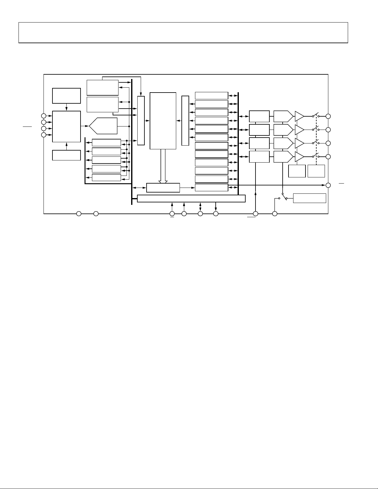
FUNCTIONAL BLOCK DIAGRAM
INTERNAL
TEMPERATURE
VALUE REGISTER
EXTERNAL
TEMPERATURE
VALUE REGISTER
A-TO-D
CONVERTER
V
DD
VALUE REGISTER
AIN1
VALUE REGISTER
AIN2
VALUE REGISTER
AIN3
VALUE REGISTER
AIN4
VALUE REGISTER
D+/AIN1
D–/AIN2
LDAC/AIN3
AIN4
7
8
9
14
ON-CHIP
TEMPERATURE
SENSOR
ANALOG
MUX
V
DD
SENSOR
COMPARATOR
DIGITAL MUX
LIMIT
STATUS
REGISTERS
ADDRESS POINTER
REGISTER
T
HIGH
REGISTERS
T
LOW
REGISTERS
VCCLIMIT
REGISTERS
AIN
DIGITAL MUX
SPI/SMBus INTERFACE
HIGH
REGISTERS
AIN
LOW
REGISTERS
CONTROL CONFIG. 1
REGISTER
CONTROL CONFIG. 2
REGISTER
CONTROL CONFIG. 3
REGISTER
DAC CONFIGURATION
REGISTERS
LDAC CONFIGURATION
REGISTERS
INTERRUPT MASK
REGISTERS
LIMIT
LIMIT
LIMIT
LIMIT
ADT7516/ADT7517/ADT7519
DAC A
REGISTERS
DAC B
REGISTERS
DAC C
REGISTERS
DAC D
REGISTERS
STRING
DAC A
STRING
DAC B
STRING
DAC C
STRING
DAC D
GAIN
SELECT
LOGIC
INTERNAL
REFERENCE
POWER-
DOWN
LOGIC
16
15
10
2
1
V
OUT
V
OUT
V
OUT
V
OUT
INT/INT
-A
-B
-C
-D
12
5
6
GND
V
DD
13
4
SCL
CS
SDA
11
ADD
9
LDAC/AIN33V
REF
-IN
Figure 6.
02883-A-001
Rev. A | Page 8 of 44

ADT7516/ADT7517/ADT7519
ABSOLUTE MAXIMUM RATINGS
Table 3.
Parameter Rating
VDD to GND –0.3 V to +7 V
Analog Input Voltage to GND –0.3 V to VDD + 0.3 V
Digital Input Voltage to GND –0.3 V to VDD + 0.3 V
Digital Output Voltage to GND –0.3 V to VDD + 0.3 V
Reference Input Voltage to GND –0.3 V to VDD + 0.3 V
Operating Temperature Range –40°C to +120°C
Storage Temperature Range –65°C to +150°C
Junction Temperature 150°C
16-Lead QSOP Package
Power Dissipation
Thermal Impedance
θ
Junction-to-Ambient 105.44°C/W
JA
θ
Junction-to-Case 38.8°C/W
JC
IR Reflow Soldering
Peak Temperature 220°C (0°C/5°C)
Time at Peak Temperature 10 sec to 20 sec
Ramp-Up Rate 2°C/sec to 3°C/sec
Ramp-Down Rate –6°C/sec
1
2
(TJ max – TA)/θ
JA
Table 4. I
2
C Address Selection
ADD Pin I2C Address
Low 1001 000
Float 1001 010
High 1001 011
Stresses above those listed under Absolute Maximum Ratings
may cause permanent damage to the device. This is a stress
rating only; functional operation of the device at these or any
other conditions above those indicated in the operational
section of this specification is not implied. Exposure to absolute
maximum rating conditions for extended periods may affect
device reliability.
1
Values relate to package being used on a 4-layer board.
2
Junction-to-case resistance is applicable to components featuring a
preferential flow direction, e.g., components mounted on a heat sink.
Junction-to-ambient resistance is more useful for air cooled PCB-mounted
components.
ESD CAUTION
ESD (electrostatic discharge) sensitive device. Electrostatic charges as high as 4000 V readily accumulate on
the human body and test equipment and can discharge without detection. Although this product features
proprietary ESD protection circuitry, permanent damage may occur on devices subjected to high energy
electrostatic discharges. Therefore, proper ESD precautions are recommended to avoid performance
degradation or loss of functionality.
Rev. A | Page 9 of 44
ADT7516/ADT7517/ADT7519
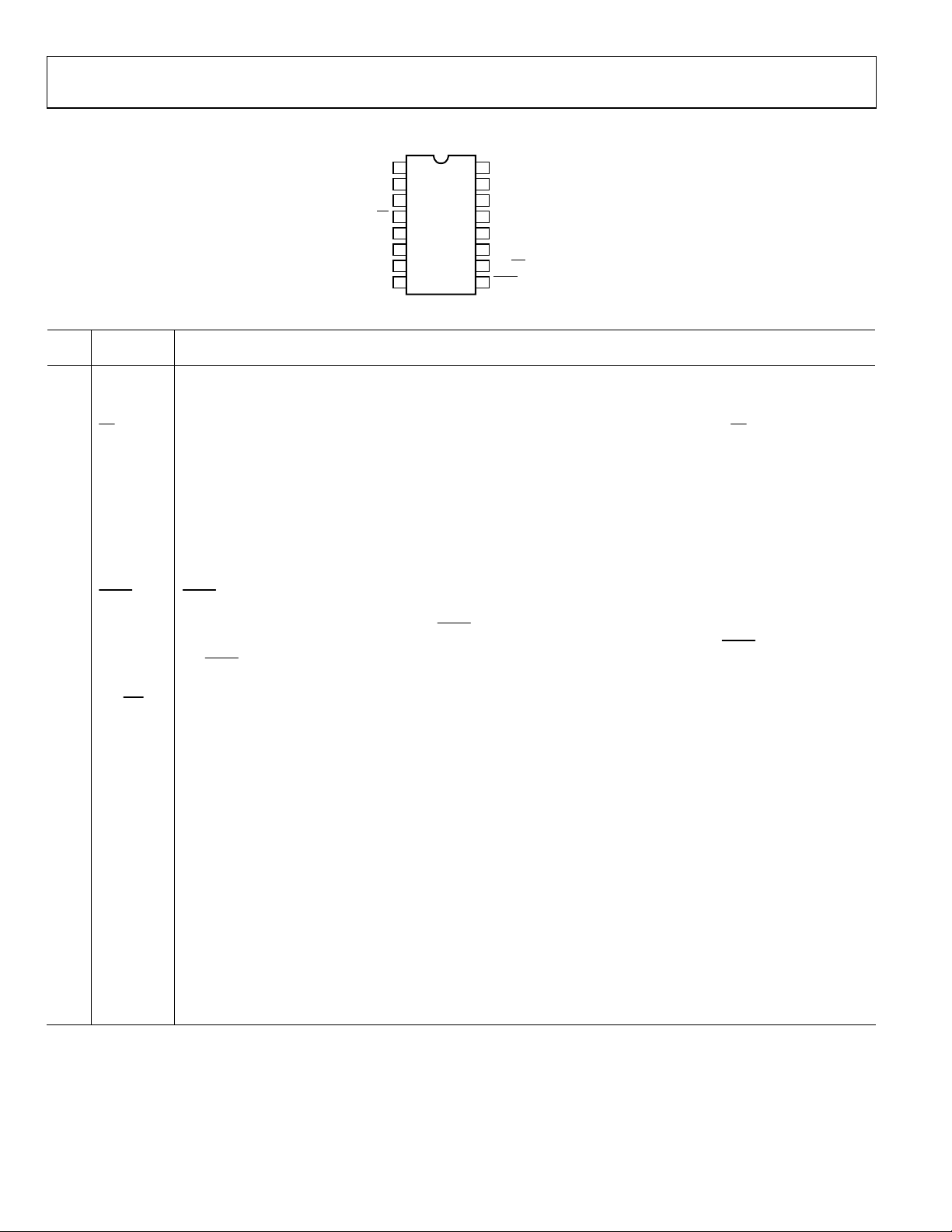
PIN CONFIGURATION AND FUNCTIONAL DESCRIPTIONS
-B
1
V
OUT
V
-A
2
OUT
V
REF
D+/AIN1
D–/AIN2
-IN
CS
GND
V
DD
ADT7516/
3
ADT7517/
ADT7519
4
TOP VIEW
5
(Not to Scale)
6
7
8
Figure 7. Pin Configuration (QSOP Package)
Table 5. Pin Function Descriptions
Pin
No.
Mnemonic Description
1 V
2 V
3 V
4
-B Buffered Analog Output Voltage from DAC B. The output amplifier has rail-to-rail operation.
OUT
-A Buffered Analog Output Voltage from DAC A. The output amplifier has rail-to-rail operation.
OUT
-IN Reference Input Pin for All Four DACs. This input is buffered and has an input range from 1 V to VDD.
REF
CS SPI Active Low Control Input. This is the frame synchronization signal for the input data. When CS goes low, it enables
the input register, and data is transferred in on the rising edges and out on the falling edges of the subsequent serial
clocks. It is recommended that this pin be tied high to V
5 GND Ground Reference Point for All Circuitry on the Part. Analog and digital ground.
6 VDD Positive Supply Voltage, 2.7 V to 5.5 V. The supply should be decoupled to ground.
7 D+/AIN1 D+. Positive Connection to External Temperature Sensor.
AIN1. Analog Input. Single-ended analog input channel. Input range is 0 V to 2.28 V or 0 V to V
8 D–/AIN2 D–. Negative Connection to External Temperature Sensor.
AIN2. Analog Input. Single-ended analog input channel. Input range is 0 V to 2.28 V or 0 V to V
9
LDAC/AIN3 LDAC. Active Low Control Input. Transfers the contents of the input registers to their respective DAC registers. A
falling edge on this pin forces any or all DAC registers to be updated if the input registers have new data. A minimum
pulse width of 20 ns must be applied to the
LDAC pin to ensure proper loading of a DAC register. This allows simul-
taneous update of all DAC outputs. Bit C3 of the Control Configuration 3 register enables the
LDAC pin controlling the loading of the DAC registers.
the
AIN3. Analog Input. Single-ended analog input channel. Input range is 0 V to 2.28 V or 0 V to V
10
11 DOUT/ADD
INT Over Limit Interrupt. The output polarity of this pin can be set to give an active low or active high interrupt when
INT/
temperature,V
, or AIN limits are exceeded. The default is active low. Open-drain output—needs a pull-up resistor.
DD
SPI Serial Data Output. Logic output. Data is clocked out of any register at this pin. Data is clocked out on the falling
edge of SCLK. Open-drain output—needs a pull-up resistor.
2
ADD. I
C Serial Bus Address Selection Pin. Logic input. A low on this pin gives the address 1001 000; leaving it floating
gives the address 1001 010; and setting it high gives the address 1001 011. The I
not latched by the device until after this address has been sent twice. On the eighth SCL cycle of the second valid
communication, the serial bus address is latched in. Any subsequent changes on this pin will have no effect on the I
serial bus address.
12 SDA/DIN
2
C Serial Data Input/Output. I2C serial data to be loaded into the part’s registers and read from these registers is
SDA. I
provided on this pin. Open-drain configuration—needs a pull-up resistor.
DIN. SPI Serial Data Input. Serial data to be loaded into the part’s registers is provided on this pin. Data is clocked into
a register on the rising edge of SCLK. Open-drain configuration—needs a pull-up resistor.
13 SCL/SCLK
Serial Clock Input. This is the clock input for the serial port. The serial clock is used to clock data out of any register of
the ADT7516/ADT7517/ADT7519 and also to clock data into any register that can be written to. Open-drain
configuration—needs a pull-up resistor.
14 AIN4 Analog Input. Single-ended analog input channel. Input range is 0 V to 2.28 V or 0 V to VDD.
15 V
16 V
-D Buffered Analog Output Voltage from DAC D. The output amplifier has rail-to-rail operation.
OUT
-C Buffered Analog Output Voltage from DAC C. The output amplifier has rail-to-rail operation.
OUT
V
-C
16
OUT
V
-D
15
OUT
14
AIN4
13
SCL/SCLK
12
SDA/DIN
11
DOUT/ADD
10
INT/INT
9
LDAC/AIN3
when operating the serial interface in I2C mode. -
DD
02883-A-006
2
C address set up by the ADD pin is
.
DD
.
DD
LDAC pin. Default is with
.
DD
2
C
Rev. A | Page 10 of 44

ADT7516/ADT7517/ADT7519
TERMINOLOGY
Relative Accuracy
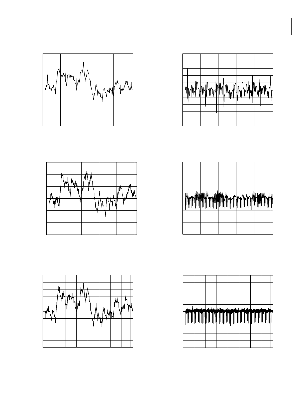
Relative accuracy or integral nonlinearity (INL) is a measure of
the maximum deviation, in LSBs, from a straight line passing
through the endpoints of the transfer function. Typical INL
versus code plots can be seen in Figure 10, Figure 11, and
Figure 12.
Differential Nonlinearity
Differential nonlinearity (DNL) is the difference between the
measured change and the ideal 1 LSB change between any two
adjacent codes. A specified differential nonlinearity of ±0.9 LSB
maximum ensures monotonicity. Typical DAC DNL versus code
plots can be seen in Figure 13, Figure 14, and Figure 15.
Total Unadjusted Error (TUE)
Total unadjusted error is a comprehensive specification that
includes the sum of the relative accuracy error, gain error, and
offset error under a specified set of conditions.
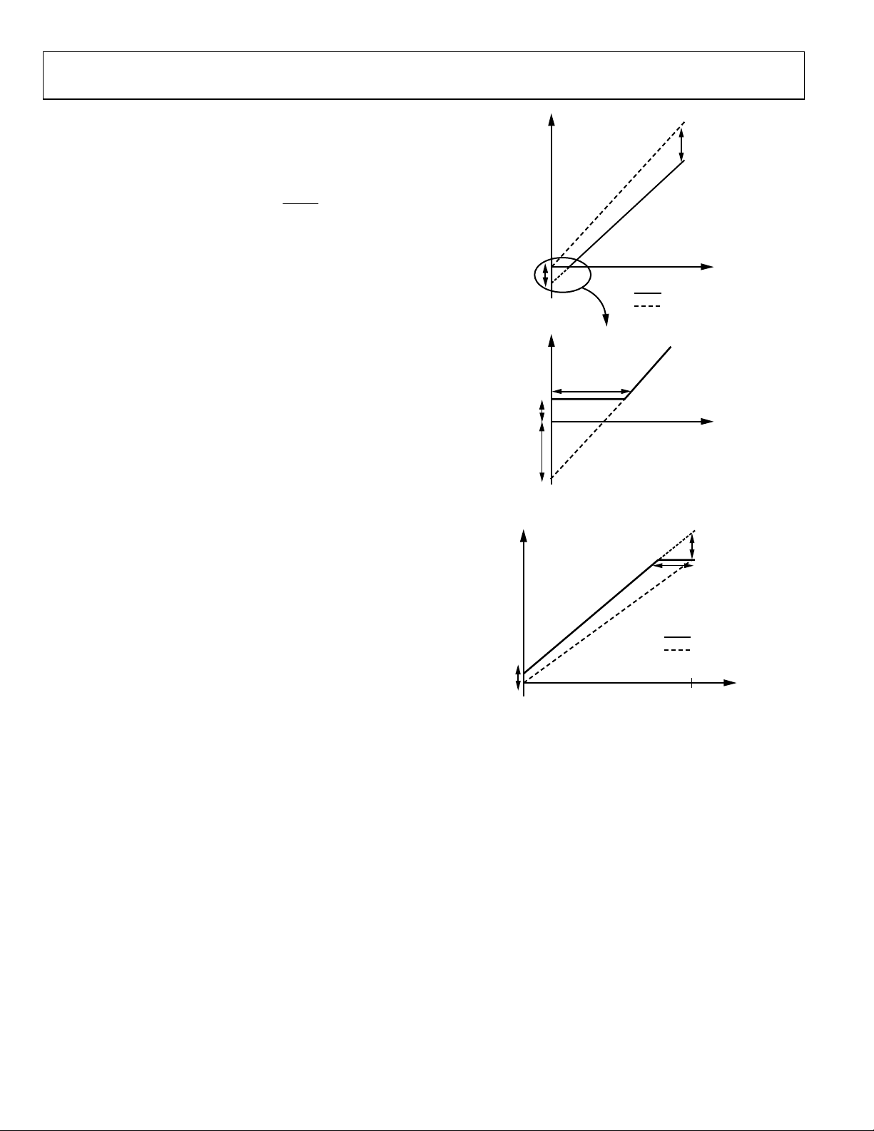
Offset Error
This is a measure of the offset error of the DAC and the output
amplifier (See Figure 8 and Figure 9). It can be negative or
positive, and it is expressed in mV.
Offset Error Match
This is the difference in offset error between any two channels.
Gain Error
This is a measure of the span error of the DAC. It is the
deviation in slope of the actual DAC transfer characteristic
from the ideal expressed as a percentage of the full-scale range.
Gain Error Match
This is the difference in gain error between any two channels.
Offset Error Drift
This is a measure of the change in offset error with changes in
temperature. It is expressed in (ppm of full-scale range)/°C.
Gain Error Drift
This is a measure of the change in gain error with changes in
temperature. It is expressed in (ppm of full-scale range)/°C.
Long Term Temperature Drift
This is a measure of the change in temperature error with the
passage of time. It is expressed in °C. The concept of long-term
stability has been used for many years to describe the amount
an IC’s parameter would shift during its lifetime. This is a
concept that has typically been applied to both voltage
references and monolithic temperature sensors. Unfortunately,
integrated circuits cannot be evaluated at room temperature
(25°C) for 10 years or so to determine this shift. Manufacturers
perform accelerated lifetime testing of integrated circuits by
operating ICs at elevated temperatures (between 125°C and
150°C) over a shorter period (typically between 500 and 1000
hours). As a result, the lifetime of an integrated circuit is
significantly accelerated due to the increase in rates of reaction
within the semiconductor material.
DC Power Supply Rejection Ratio (PSRR)
This indicates how the output of the DAC is affected by changes
in the supply voltage. PSRR is the ratio of the change in V
a change in V
in dB. V
for full-scale output of the DAC. It is measured
DD
is held at 2 V and VDD is varied ±10%.
REF
OUT
to
DC Crosstalk
This is the dc change in the output level of one DAC in response
to a change in the output of another DAC. It is measured with a
full-scale output change on one DAC while monitoring another
DAC. It is expressed in µV.
Reference Feedthrough
This is the ratio of the amplitude of the signal at the DAC
output to the reference input when the DAC output is not being
updated (i.e., LDAC is high). It is expressed in dB.
Channel-to-Channel Isolation
This is the ratio of the amplitude of the signal at the output of
one DAC to a sine wave on the reference input of another DAC.
It is measured in dB.
Major-Code Transition Glitch Energy
Major-code transition glitch energy is the energy of the impulse
injected into the analog output when the code in the DAC
register changes state. It is normally specified as the area of the
glitch in nV-s and is measured when the digital code is changed
by 1 LSB at the major carry transition (011 . . . 11 to 100 . . . 00 or
100 . . . 00 to 011 . . . 11).
Digital Feedthrough
Digital feedthrough is a measure of the impulse injected into
the analog output of a DAC from the digital input pins of the
device but is measured when the DAC is not being written to. It
is specified in nV-s and is measured with a full-scale change on
the digital input pins, i.e., from all 0s to all 1s or vice versa.
Digital Crosstalk
This is the glitch impulse transferred to the output of one DAC
at midscale in response to a full-scale code change (all 0s to all
1s and vice versa) in the input register of another DAC. It is
measured in standalone mode and is expressed in nV-s.
Analog Crosstalk
This is the glitch impulse transferred to the output of one DAC
due to a change in the output of another DAC. It is measured by
loading one of the input registers with a full-scale code change
(all 0s to all 1s and vice versa) while keeping
LDAC
pulse
digital code was not changed. The area of the glitch is expressed
in nV-s.
low and monitor the output of the DAC whose
LDAC
high. Then
Rev. A | Page 11 of 44
ADT7516/ADT7517/ADT7519
DAC-to-DAC Crosstalk
This is the glitch impulse transferred to the output of one DAC
due to a digital code change and subsequent output change of
another DAC. This includes both digital and analog crosstalk. It
is measured by loading one of the DACs with a full-scale code
LDAC
change (all 0s to all 1s and vice versa) with
monitoring the output of another DAC. The energy of the glitch
is expressed in nV-s.
Multiplying Bandwidth
The amplifiers within the DAC have a finite bandwidth. The
multiplying bandwidth is a measure of this. A sine wave on the
reference (with full-scale code loaded to the DAC) appears on
the output. The multiplying bandwidth is the frequency at
which the output amplitude falls to 3 dB below the input.
Total Harmonic Distortion
This is the difference between an ideal sine wave and its
attenuated version using the DAC. The sine wave is used as the
reference for the DAC, and the THD is a measure of the
harmonics present on the DAC output, expressed in dB.
Round Robin
This term is used to describe the ADT7516/ADT7517/
ADT7519 cycling through the available measurement channels
in sequence, taking a measurement on each channel.
DAC Output Settling Time
This is the time required, following a prescribed data change, for
the output of a DAC to reach and remain within ±0.5 LSB of the
final value. A typical prescribed change is from 1/4 scale to
3/4 scale.
low and
OUTPUT
VOLTAGE
NEGATIVE
OFFSET
ERROR
AMPLIFIER
FOOTROOM
NEGATIVE
OFFSET
ERROR
LOWER
DEADBAND
CODES
DAC CODE
Figure 8. DAC Transfer Function with Negative Offset
OUTPUT
VOLTAGE
POSITIVE
OFFSET
ERROR
DAC CODE FULL SCALE
Figure 9. DAC Transfer Function with Positive Offset (V
GAIN ERROR
OFFSET ERROR
ACTUAL
IDEAL
GAIN ERROR
OFFSET ERROR
UPPER
DEADBAND
CODES
ACTUAL
IDEAL
+
02883-A-007
+
02883-A-008
= VDD)
REF
Rev. A | Page 12 of 44
ADT7516/ADT7517/ADT7519
TYPICAL PERFORMANCE CHARACTERISTICS
0.20
0.15
0.10
0.05
0
–0.05
INL ERROR (LSB)
–0.10
–0.15
–0.20
0 50 100 150 200 250
DAC CODE
02883-A-009
0.10
0.08
0.06
0.04
0.02
0
–0.02
DNL ERROR (LSB)
–0.04
–0.06
–0.08
–0.10
0 50 100 150 200 250
DAC CODE
02883-A-012
Figure 10. ADT7519 Typical DAC INL Plot
0.6
0.4
0.2
0
INL ERROR (LSB)
–0.2
–0.4
–0.6
0 200 400 600
Figure 11. ADT7517 Typical DAC INL Plot
2.5
2.0
1.5
1.0
0.5
0
–0.5
INL ERROR (LSB)
–1.0
–1.5
–2.0
–2.5
Figure 12. ADT7516 Typical DAC INL Plot
DAC CODE
800 1000
20001500500 10000 2500 3000 3500 4000
DAC CODE
Figure 13. ADT7519 Typical DAC DNL Plot
0.3
0.2
0.1
0
–0.1
DNL ERROR (LSB)
–0.2
02883-A-010
–0.3
0 200 400 600 800 1000
DAC CODE
02883-A-013
Figure 14. ADT7517 Typical DAC DNL Plot
1.0
0.8
0.6
0.4
0.2
0
–0.2
DNL ERROR (LSB)
–0.4
–0.6
–0.8
02883-A-011
–1.0
20001500500 10000 2500 3000 3500 4000
DAC CODE
02883-A-014
Figure 15. ADT7516 Typical DAC DNL Plot
Rev. A | Page 13 of 44
ADT7516/ADT7517/ADT7519
0.30
10
0.25
0.20
0.15
0.10
0.05
ERROR (LSB)
0
–0.05
–0.10
1.0 1.5 2.0 2.5 3.0 3.5 4.0 4.5 5.0
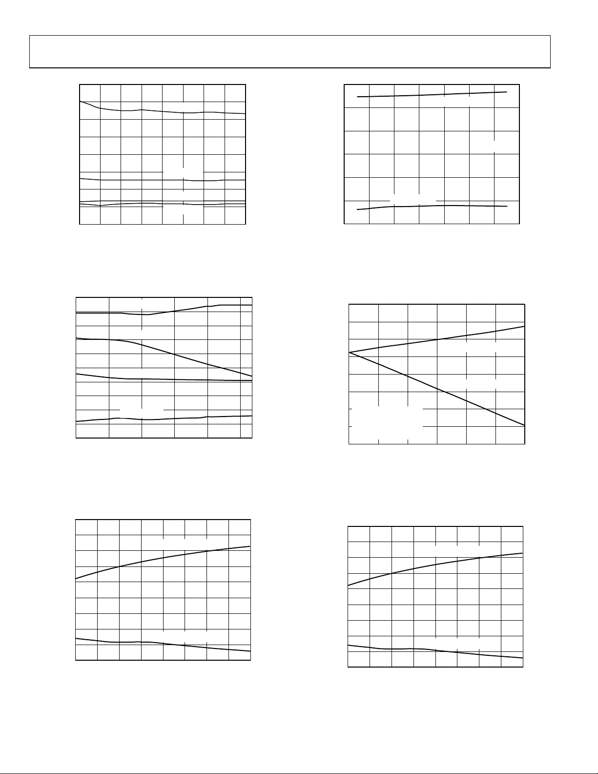
Figure 16. ADT7519 DAC INL and DNL Error vs. V
0.14
0.12
0.10
0.08
0.06
0.04
0.02
ERROR (LSB)
0
–0.02
–0.04
–0.06
–40 110805020–10
INL WCP
INL WCN
DNL WCP
DNL WCN
TEMPERATURE (°C)
INL WCP
DNL WCP
DNL WCN
INL WCN
V
(V)
REF
REF
Figure 17. ADT7519 DAC INL Error and DNL Error vs. Temperature
5
0
–5
ERROR (LSB)
–10
–15
02883-A-015
–20
2.7 3.3 3.6 4.0
GAIN ERROR
Figure 19. DAC Offset Error and Gain Error vs. V
2.505
2.500
2.495
2.490
2.485
2.480
DAC OUTPUT (V)
2.475
VDD=5V
=5V
V
REF
DAC OUTPUT
2.470
02883-A-016
LOADED TO MIDSCALE
2.465
0123
Figure 20. DAC V
Source and Sink Current Capability
OUT
OFFSET ERROR
V
(V)
DD
SOURCE CURRENT
CURRENT (mA)
V
= 2.25V
REF
4.5 5.0
SINK CURRENT
45
02883-A-018
5.5
DD
02883-A-019
6
0
–0.2
–0.4
–0.6
–0.8
–1.0
ERROR (LSB)
–1.2
–1.4
–1.6
–1.8
–40 120100806040200–20
OFFSET ERROR
GAIN ERROR
TEMPERATURE (°C)
Figure 18. DAC Offset Error and Gain Error vs. Temperature
02883-A-017
Rev. A | Page 14 of 44
ERROR (LSB)
–0.2
–0.4
–0.6
–0.8
–1.0
–1.2
–1.4
–1.6
–1.8
0
–40 120100806040200–20
TEMPERATURE (
Figure 21. Supply Current vs. DAC Code
OFFSET ERROR
GAIN ERROR
°
C)
02883-A-017
 Loading...