

Temperature Sensor Hub and Fan Controller
FEATURES
Monitors up to 10 remote temperature sensors
Monitors and controls speed of up to 4 fans independently
PWM outputs drive each fan under software control
FULL_SPEED
external hardware
SMBALERT
Three-state ADDR pin allows up to 3 devices on a single bus
Temperature decoder interprets TMP05/TMP06 temperature
sensors and communicates values over I
Limit comparison of all monitored values
Supports fast I
Meets SMBus 2.0 electrical specifications
(fully SMBus 1.1-compliant)
Footprint-compatible with ADT7460
APPLICATIONS
Servers
Networking and telecommunications equipment
Desktops
input allows fans to be blasted PWMMAX by
interrupt signals failures to system controller
2
C bus
2
C standard (400 kHz max)
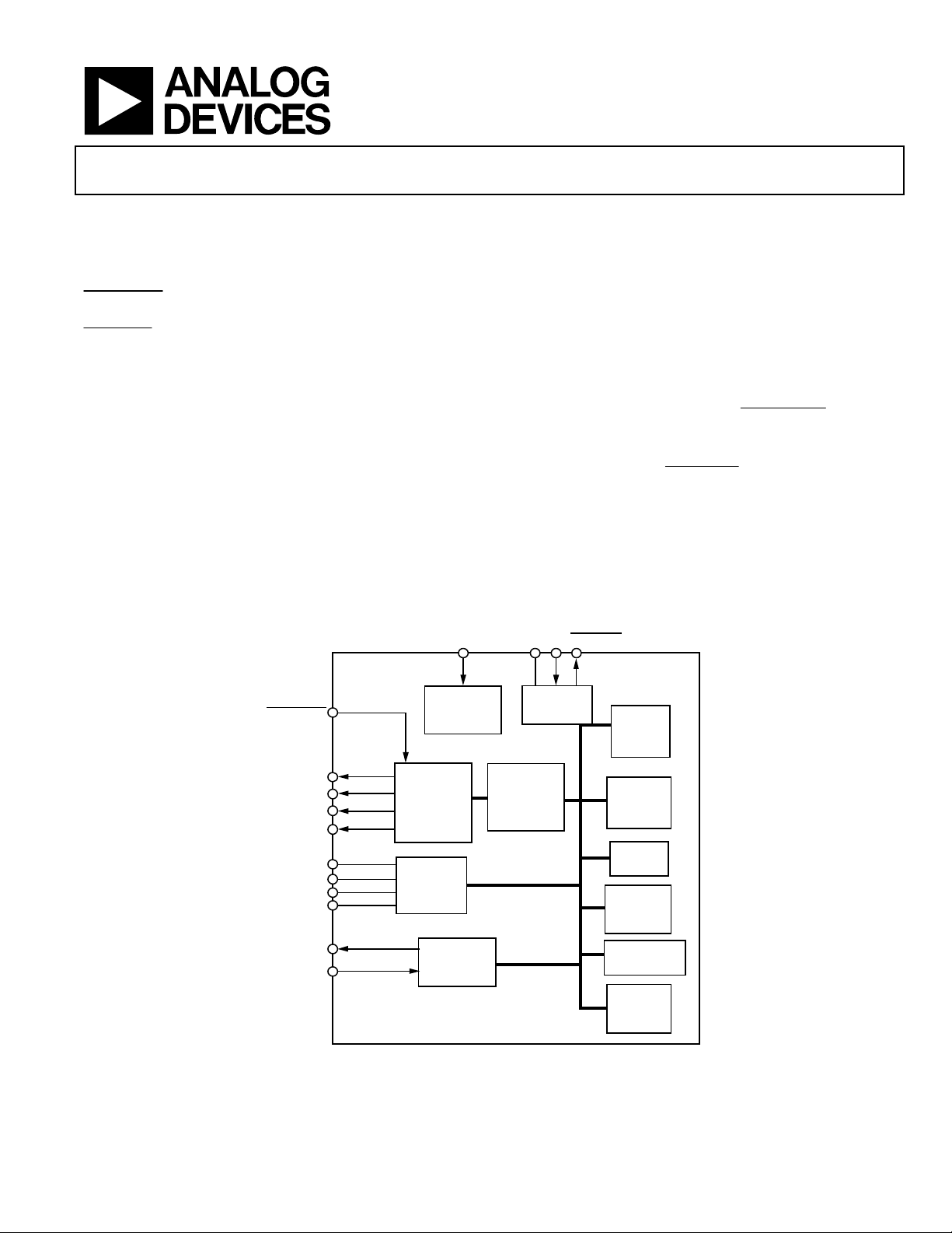
FUNCTIONAL BLOCK DIAGRAM
ADDR SDASCL
ADT7470
GENERAL DESCRIPTION
The ADT7470 controller is a multichannel temperature sensor
and PWM fan controller and fan speed monitor for noisesensitive systems requiring active system cooling. It is designed
to interface directly to an I
using a service processor. The aim is to quickly develop systems
that are modular and can easily be expanded depending on the
system’s cooling requirements. The device can monitor up to
10 temperature sensors. It can also monitor and control the
speed of four fans so that they operate at the lowest possible
speed for minimum acoustic noise. A
provided to allow the fans to be “blasted” to PWMMAX via
external hardware control, under extreme thermal conditions,
or on system startup. An
error conditions such as fan underspeed and fan failure to the
system service processor. Individual error conditions can then be
read from status registers over the I
failure condition, any or all PWM outputs can be programmed
to automatically adjust to PWMMAX to provide fail-safe
cooling.
SMBALERT
2
C bus and control/monitor the fans
SMBALERT
2
C bus. In the event of a fan
FULL_SPEED
interrupt communicates
input is
ADT7470
FULL_SPEED
PWM1
PWM2
PWM3
PWM4
TACH1
TACH2
TACH3
TACH4
TMP_START
TMP_IN
SMBus
ADDRESS
SELECTION
PWM
REGISTERS
AND
CONTROLLERS
FAN SPEED
COUNTERS
TEMPERATURE
DECODER
SERIAL BUS
INTERFACE
AUTOMATIC
FAN SPEED
CONTROL
ADDRESS
POINTER
REGISTER
PWM
CONFIG
REGISTERS
INTERRUPT
MASKING
INTERRUPT
STATUS
REGISTERS
LIMIT
COMPARATORS
VALUE AND
LIMIT
REGISTERS
Figure 1.
Protected by Patent Numbers US6,188,189, US6,169,442, US6,097,239, US5,982,221, US5,867,012. Other patents pending.
Rev. A
Information furnished by Analog Devices is believed to be accurate and reliable.
However, no responsibility is assumed by Analog Devices for its use, nor for any
infringements of patents or other rights of third parties that may result from its use.
Specifications subject to change without notice. No license is granted by implication
or otherwise under any patent or patent rights of Analog Devices. Trademarks and
registered trademarks are the property of their respective owners.
One Technology Way, P.O. Box 9106, Norwood, MA 02062-9106, U.S.A.
Tel: 781.329.4700
Fax: 781.326.8703 © 2005 Analog Devices, Inc. All rights reserved.
www.analog.com
04684-0-001

ADT7470
TABLE OF CONTENTS
Specifications..................................................................................... 3
Absolute Maximum Ratings............................................................ 5
Thermal Characteristics .............................................................. 5
ESD Caution.................................................................................. 5
Pin Configuration and Function Descriptions............................. 6
Functional Description .................................................................... 7
General Description..................................................................... 7
Fan Speed Measurement.............................................................. 7
ADT7470 Address Selection....................................................... 7
Internal Registers of the ADT7470 ............................................ 7
SMBus/I
ADT7470 Write Operations...................................................... 10
ADT7470 Read Operations....................................................... 11
SMBus Timeout .......................................................................... 11
General-Purpose I/O Pins (Open Drain) ............................... 11
2
C Communications Interface..................................... 7
8-Bit Limits.................................................................................. 14
16-Bit Limits ............................................................................... 14
Out-of-Limit Comparisons....................................................... 15
Monitoring Cycle Time ............................................................. 16
Status Registers ........................................................................... 16
SMBALERT
Handling
Masking Interrupt Sources........................................................ 18
Enabling the
Fan Drive Using PWM Control.................................................... 19
Fan Speed Measurement................................................................ 20
Tac h Input s .................................................................................. 20
Fan Speed Measurement ........................................................... 20
Fan Speed Control.......................................................................... 23
PWM Logic State........................................................................ 23
Interrupt Behavior ............................................... 17
SMBALERT
SMBALERT
Interrupts............................................. 17
Interrupt Output ........................... 18
Temperature Measurement Using TMP05/TMP06................... 12
Measuring Temperature ............................................................ 12
TMP05/TMP06 Decoder........................................................... 12
Interrupt Functionality and Status Registers ..............................14
Limit Values................................................................................. 14
REVISION HISTORY
2/05—Rev. 0 to Rev. A
Added General-Purpose I/O Pins (Open Drain) Section......... 11
11/04—Revision 0: Initial Version
Manual Fan Speed Control ....................................................... 23
Automatic Fan Speed Control .................................................. 23
ADT7470 Registers ........................................................................ 24
Outline Dimensions ....................................................................... 39
Ordering Guide .......................................................................... 39
Rev. A | Page 2 of 40

ADT7470
SPECIFICATIONS
TA = T
Table 1.
Parameter Min Typ Max Unit Test Conditions/Comments
POWER SUPPLY
FAN RPM-TO-DIGITAL CONVERTER
329 RPM Fan count = 0x3FFF
5,000 RPM Fan count = 0x0438
10,000 RPM Fan count = 0x021C
OPEN-DRAIN DIGITAL OUTPUTS, PWM1–PWM4, SMBALERT
OPEN-DRAIN SERIAL DATA BUS OUTPUT (SDA)
SMBus DIGITAL INPUTS (SCL, SDA)
DIGITAL INPUT LOGIC LEVELS (TACH INPUTS, FULL_SPEED, GPIO)
DIGITAL INPUT LOGIC LEVELS (TMP_IN)
DIGITAL INPUT CURRENT
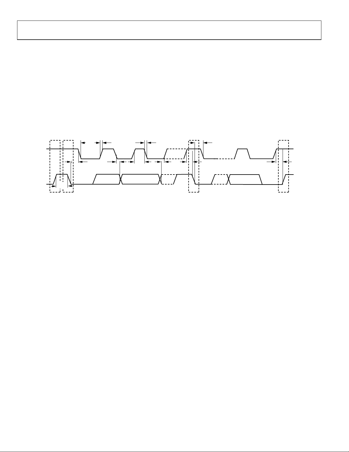
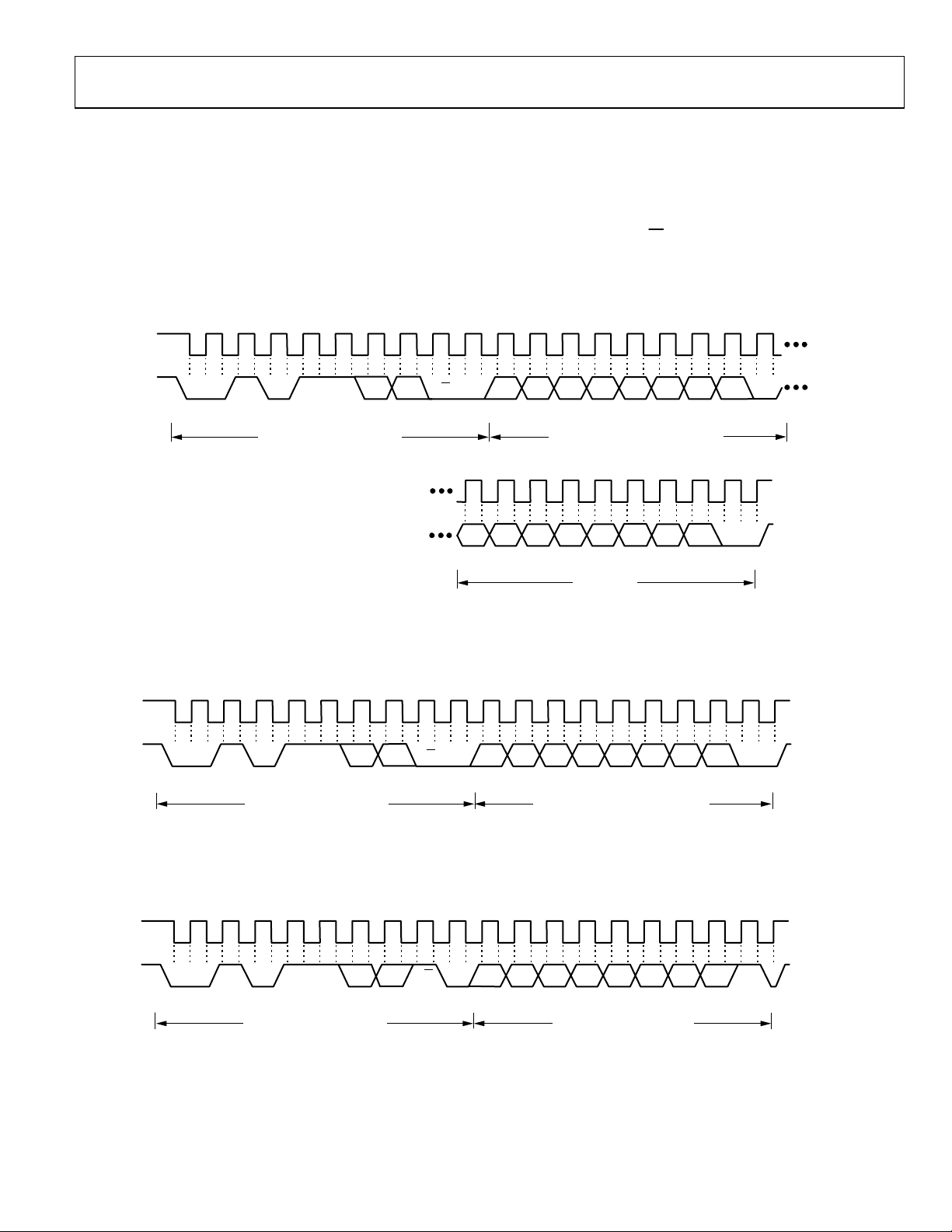
SERIAL BUS TIMING
1
VDD should never be floated in the presence of SCL/SDA activity. Charge injection can be sufficient to induce approximately 0.6 V on VDD.
MIN
to T
, VCC = V
MAX
1
MIN
to V
, unless otherwise noted. T
MAX
= −40oC, T
MIN
= +125oC.
MAX
Supply Voltage 3.0 3.3 5.5 V
Supply Current, I
Standby Current, I
CC
CC
0.5 0.8 mA
4 µA
Accuracy ±12 %
Full-Scale Count 65,535
Nominal Input RPM 109 RPM Fan count = 0xBFFF
Output Low Voltage, V
OL
High Level Output Current, I
Output Low Voltage, V
OL
High Level Output Current, I
Input High Voltage, V
Input Low Voltage, V
IH
IL
OH
OH
0.4 V I
0.1 1 µA V
0.4 V I
0.1 1 µA V
= –8.0 mA, VCC = +3.3 V
OUT
= V
OUT
= –4.0 mA, VCC = +3.3 V
OUT
= V
OUT
2.4 V
0.4 V
CC
CC
Hysteresis 500 mV
Input High Voltage, V
Input Low Voltage, V
IH
IL
2.4 V
0.8 V
Hysteresis 50 mV p-p
Input High Voltage, V
Input Low Voltage, V
Input High Current, I
Input Low Current, I
Input Capacitance, C
Clock Frequency, f
Glitch Immunity, t
Bus Free Time, t
Start Setup Time, t
Start Hold Time, t
SCL Low Time, t
SCL High Time, t
SCL, SDA Rise Time, t
SCL, SDA Fall Time, t
Data Setup Time, t
Data Hold Time, t
IH
IL
IH
IL
IN
SCLK
SW
BUF
SU;STA
HD;STA
LOW
HIGH
r
f
SU;DAT
HD;DAT
Detect Clock Low Timeout, t
TIMEOUT
VDD – 0.3 V
0.4 V
–5 µA VIN = V
CC
5 µA VIN = 0
5 pF
400 kHz See Figure 2
50 ns See Figure 2
1.3 µs See Figure 2
600 ns See Figure 2
600 ns See Figure 2
1.3 µs See Figure 2
0.6 µs See Figure 2
300 ns See Figure 2
300 ns See Figure 2
100 ns See Figure 2
300 ns See Figure 2
25 28 31 ms Can be optionally disabled
Rev. A | Page 3 of 40
ADT7470
Note the following about the specifications for the ADT7470:
• All voltages are measured with respect to GND, unless otherwise specified.
• Typical values are at T
= 25°C and represent most likely parametric norm.
A
• Logic inputs accept input high voltages up to 5 V even when the device is operating at supply voltages below 5 V.
• V
• Timing specifications are tested at logic levels of V
should never be floated in the presence of SCL/SDA activity. Charge injection can be sufficient to induce approximately 0.6 V
DD
.
on V
DD
= 0.8 V for a falling edge and VIH = 2.0 V for a rising edge.
IL
SCL
SDA
t
BUF
PS
t
HD;STA
t
LOW
t
R
t
HD;DAT
t
F
t
HIGH
t
SU;DAT
SP
Figure 2. Serial Bus Timing Diagram
t
SU;STA
t
HD;STA
t
SU;STO
04684-0-002
Rev. A | Page 4 of 40

ADT7470
ABSOLUTE MAXIMUM RATINGS
Table 2.
Parameter Rating
Positive Supply Voltage (VCC) 6.5 V
Voltage on Any Tach or PWM Pin –0.3 V to +6.5 V
Voltage on Any Input or Output Pin –0.3 V to VCC + 0.3 V
Maximum Junction Temperature (TJ max) 150°C
Storage Temperature Range –65°C to +150°C
Lead Temperature, Soldering
Vapor Phase, 60 sec 215°C
Infrared, 15 sec 200°C
ESD Rating 3000 V
ESD CAUTION
ESD (electrostatic discharge) sensitive device. Electrostatic charges as high as 4000 V readily accumulate on
the human body and test equipment and can discharge without detection. Although this product features
proprietary ESD protection circuitry, permanent damage may occur on devices subjected to high energy
electrostatic discharges. Therefore, proper ESD precautions are recommended to avoid performance
degradation or loss of functionality.
Stresses above those listed under Absolute Maximum Ratings
may cause permanent damage to the device. This is a stress
rating only; functional operation of the device at these or any
other conditions above those indicated in the operational
section of this specification is not implied. Exposure to absolute
maximum rating conditions for extended periods may affect
device reliability.
THERMAL CHARACTERISTICS
16-Lead QSOP package:
= 105°C/W
θ
JA
= 39°C/W
θ
JC
Rev. A | Page 5 of 40
ADT7470
PIN CONFIGURATION AND FUNCTION DESCRIPTIONS
SCL
GND
V
TACH3
PWM2
TACH1
TACH2
PWM3
CC
1
2
3
ADT7470
4
TOP VIEW
5
(Not to Scale)
6
7
8
16
SDA
15
PWM1
14
SMBALERT
13
FULL_SPEED/TMP_START
12
TMP_IN
11
ADDR
PWM4
10
9
TACH4
04684-0-003
Figure 3. Pin Configuration
Table 3. Pin Function Descriptions
Pin No. Mnemonic Description
1 SCL Digital Input (Open Drain). SMBus serial clock input. Requires SMBus pull-up.
2 GND Ground Pin for the ADT7470.
3 V
CC
Power Supply Pin. Can be powered by 3.3 V standby if operation in low power states is required.
4 TACH3 Digital Input (Open Drain). Fan tachometer input to measure the speed of Fan 3.
5 PWM2
Digital I/O (Open Drain). Requires 10 kΩ typical pull-up. Pulse-width modulated output to control the speed of
Fan 2. Can be configured as GPIO by setting Bit 0x7F<2> = 1.
6 TACH1 Digital Input (Open Drain). Fan tachometer input to measure the speed of Fan 1.
7 TACH2 Digital Input (Open Drain). Fan tachometer input to measure the speed of Fan 2.
8 PWM3
Digital I/O (Open Drain). Pulse-width modulated output to control the speed of Fan 3. Requires 10 kΩ typical
pull-up. Can be configured as GPIO by setting Bit 0x7F<1> = 1.
9 TACH4 Digital Input (Open Drain). Fan tachometer input to measure the speed of Fan 4.
10 PWM4
Digital I/O (Open Drain). Pulse-width modulated output to control the speed of Fan 4. Requires 10 kΩ typical
pull-up. Can be configured as GPIO by setting Bit 0x7F<0> = 1.
11 ADDR Three-state Input. Used to set the SMBus device address.
12 TMP_IN
Digital Input (Open Drain). PWM input to PWM processing engine that interprets daisy-chained output from
multiple TMP05 temperature sensors. Readings from individual TMP05 temperature sensors are available by
reading the temperature reading registers over the SMBus.
13
FULL_SPEED Digital Input Active Low (Open Drain). This input blasts the fans to PWMMAX when the pin is pulled low
externally.
13 TMP_START
Digital Output (Open Drain). This pin can be used as an output to start daisy-chained temperature
measurements from TMP05 or TMP06 temperature sensors.
14
SMBALERT Digital Output Active Low (Open Drain). This pin can be reconfigured as an SMBALERT interrupt output to
signal out-of-limit conditions such as fan failures.
15 PWM1
Digital I/O (Open Drain). Pulse-width modulated output to control the speed of Fan 1. Requires 10 kΩ typical
pull-up. Can be configured as GPIO by setting Bit 0x7F<3> = 1.
16 SDA Digital I/O (Open Drain). SMBus bidirectional serial data. Requires SMBus pull-up.
Rev. A | Page 6 of 40

ADT7470
FUNCTIONAL DESCRIPTION
GENERAL DESCRIPTION
The ADT7470 is a multichannel PWM fan controller and monitor for any system requiring monitoring and cooling. The device
communicates with the system via a serial system management
bus. The device has a single address line for address selection
(Pin 11), a serial data line for reading and writing addresses and
data (Pin 16), and an input line for the serial clock (Pin 1). All
control and programming functions of the ADT7470 are performed over the serial bus, which supports both SMBus and fast
2
C specifications. In addition, an
I
is provided to indicate out-of-limit conditions.
SMBALERT
interrupt output
FAN SPEED MEASUREMENT
When the ADT7470 monitoring sequence is started, it cycles
through each fan tach input to measure fan speed. Measured
values from these inputs are stored in value registers. These can
be read out over the serial bus, or can be compared with
programmed limits stored in the limit registers. The results of
out-of-limit comparisons are stored in the status registers,
which can be read over the serial bus to flag out-of-limit
conditions. If fan speeds drop below preset levels or a fan stalls,
an interrupt is generated and the fans can automatically blast to
PWMMAX. Likewise, the ADT7470 can flag fan overspeed
conditions by using fan tach max registers.
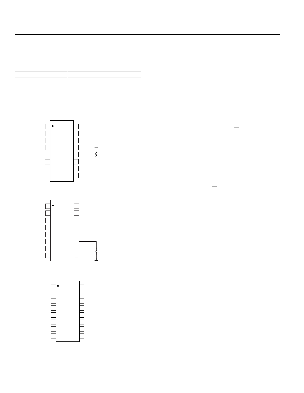
ADT7470 ADDRESS SELECTION
Pin 11 is the address selection pin, ADDR. If Pin 11 is pulled
low on power-up, the ADT7470 defaults to Slave Address 0x58
(left-justified) or 0x2C (right-justified). If Pin 11 is floating on
power-up, the ADT7470 defaults to SMBus slave Address 0x5A
(left-justified) or 0x2D (right-justified). By pulling the pin high
on power-up, the SMBus slave address is 0x5C (left-justified) or
0x2E (right-justified).
INTERNAL REGISTERS OF THE ADT7470
A brief description of the ADT7470’s principal internal registers
is given in the following sections. For detailed information on
the function of each register, see the register map in Table 21.
Configuration Registers
These registers provide control and configuration of the
ADT7470, including alternate pinout functionality such as a fan
blast input (
ment (start) output.
Address Pointer Register
This register contains the address that selects one of the other
internal registers. When writing to the ADT7470, the first byte
of data is always a register address that is written to the address
pointer register.
FULL_SPEED
) or daisy-chained TMP05 measure-
Status Registers
These registers provide status of each limit comparison and are
used to signal out-of-limit conditions on the fan speed channels,
or temperature channels if monitored using the PWM_IN
feature. If Pin 14 (
asserts low whenever a status bit is set, signaling an out-of-limit
condition.
Interrupt Mask Registers
Allows each interrupt status event to be individually masked
from driving the
where fan tach inputs are unused and left floating, or if temperature inputs from TMP05s are ignored from an interrupt
perspective. Masking interrupt status bits prevents the
SMBALERT
still reflect out-of-limit conditions. This can prevent a service
processor from being continually tied up in an interrupt service
routine if a value remains outside limits for a relatively long
duration.
Value and Limit Registers
The results of fan speed measurements are stored in these registers, along with their limit values. The limit values store the
slowest speed at which the fans are expected to run. Alternatively,
the limit value can determine the expected fan failure in terms
of running speed, in case the fan does not completely stall. If
TMP05s and TMP06s are daisy-chained in through the
PWM_IN pin, the measured temperatures are stored in
temperature value registers.
Registers
T
MIN
These registers program the starting temperature for each fan
under automatic fan speed control. The ADT7470 has limited
automatic fan speed control capability where only one mode of
operation is supported. If TMP05s are daisy-chained in, the
fastest speed calculated, determined by the measured temperature, T
on/off hysteresis is set at 4°C so that the fans turn off 4°C below
the temperature at which they turn on. This prevents fan chatter
in the system.
, and a fixed slope of 20°C can drive each fan. Fan
MIN
SMBALERT
SMBALERT
output from being driven, although the status bits
) is used in the system, this pin
output as required. This is useful
SMBus/I2C COMMUNICATIONS INTERFACE
Serial Bus Interface
Control of the ADT7470 is carried out using the serial system
management bus (SMBus). This interface is fully compatible
with SMBus 2.0 electrical specifications and meets 400 pF bus
capacitance requirements. The device also supports fast I
(400 kHz max). The ADT7470 is connected to the bus as a slave
device under the control of a master controller or service
processor.
The ADT7470 has a 7-bit serial bus address. When the device is
powered up with Pin 11 (ADDR) high, the ADT7470 has an
SMBus address of 010 1111 or 0x5E (left-justified). Because the
2
C
Rev. A | Page 7 of 40
ADT7470
address is 7 bits, it can be left- or right-justified; this determines
whether the address reads as 0x5x or 0x2x. Pin 11 can be left
floating or tied low for other addressing options, as shown in
Tabl e 4.
Table 4. ADT7470 Address Select Mode
Pin 11 (ADDR) State Address
High (10 kΩ to VCC)
Low (10 kΩ to GND)
Floating (no pull-up)
1
2
3
4
5
6
7
8
Figure 4. SMBus Address = 0x5E or 0x2F (Pin 11 = 1)
ADT7470
010 1111 (0x5E left-justified or
0x2F right-justified)
010 1100 (0x58 left-justified or
0x2C right-justified)
010 1110 (0x5C left-justified or
0x2E right-justified)
16
15
14
13
12
11
10
9
ADDR
V
CC
10kΩ
TYP
04684-0-004
The device address is sampled and latched on the first valid
SMBus transaction, so any additional attempted addressing
changes have no immediate effect. The facility to make
hardwired changes to the SMBus slave address allows the user
to avoid conflicts with other devices sharing the same serial bus,
for example, if more than one ADT7470 is used in a system.
The serial bus protocol operates as follows:
1. The master initiates data transfer by establishing a start
condition, defined as a high-to-low transition on the serial
data line, SDA, while the serial clock line, SCL, remains
high. This indicates that an address/data stream follows.
All slave peripherals connected to the serial bus respond to
the start condition, and shift in the next 8 bits, consisting
W
of a 7-bit address (MSB first) and a R/
bit. This determines
the direction of the data transfer, that is, whether data is
written to or read from the slave device.
The peripheral whose address corresponds to the transmitted address responds by pulling the data line low during
the low period before the 9th clock pulse, known as the
acknowledge bit. All other devices on the bus now remain
idle while the selected device waits for data to be read from
W
or written to it. If the R/
the slave device. If the R/
bit is a 0, the master writes to
W
bit is a 1, the master reads from
the slave device.
1
2
3
4
ADT7470
5
6
7
8
16
15
14
13
12
ADDR
11
10
9
10kΩ
TYP
04684-0-005
Figure 5. SMBus Address = 0x58 or 0x2C (Pin 11 = 0)
1
2
3
4
5
6
7
8
ADT7470
16
15
14
13
12
ADDR
11
10
9
04684-0-006
Figure 6. SMBus Address = 0x5C or 0x2E (Pin 11 = Floating)
2. Data is sent over the serial bus in sequences of 9 clock pulses,
8 bits of data followed by an acknowledge bit from the slave
device. Transitions on the data line must occur during the
low period of the clock signal and remain stable during the
high period. This is because a low-to-high transition when
the clock is high might be interpreted as a stop signal. The
number of data bytes that can be transmitted over the serial
bus in a single read or write operation is limited only by
what the master and slave devices can handle.
3. After all data bytes are read or written, stop conditions are
established. In write mode, the master pulls the data line
high during the 10th clock pulse to assert a stop condition.
In read mode, the master device overrides the acknowledge
bit by pulling the data line high during the low period before
the 9th clock pulse. This is known as No Acknowledge.
The master then takes the data line low during the low
period before the 10th clock pulse, then high during the
10th clock pulse to assert a stop condition.
Any number of bytes of data can be transferred over the serial
bus in one operation. However, it is not possible to mix read
and write in one operation, because the type of operation is
determined at the beginning and subsequently cannot be
changed without starting a new operation.
Rev. A | Page 8 of 40
ADT7470
A
A
A
In the ADT7470, write operations contain either one or two
bytes, and read operations contain one byte, and perform the
following functions.
To write data to one of the device data registers or read data
from it, the address pointer register must be set so that the
correct data register is addressed. Then data can be written into
that register or read from it. The first byte of a write operation
1
SCL
991
always contains an address that is stored in the address pointer
register. If data is to be written to the device, the write operation
contains a second data byte that is written to the register selected
by the address pointer register.
This is illustrated in Figure 7. The device address is sent over
W
the bus followed by R/
set to 0. This is followed by two data
bytes.
SD
START BY
SCL
SD
START BY
MASTER
SCL
001 1 1 A1 A0 R/W
MASTER
FRAME 1
SERIAL BUS ADDRESS
BYTE
Figure 7. Writing a Register Address to the Address Pointer Register, Then Writing Data to the Selected Register
1
01 01 1A1A0
FRAME 1
SERIAL BUS ADDRESS
BYTE
1
D7 D6 D5 D4 D3 D2 D1 D0
ACK. BY
ADT7470
ADDRESS POINTER REGISTER BYTE
1
SCL (CONTINUED)
SDA (CONTINUED)
D7 D6 D5 D4 D3 D2 D1 D0
991
R/W D7 D6 D5 D4 D3 D2 D1 D0
ACK. BY
ADT7470
ADDRESS POINTER REGISTER BYTE
Figure 8. Writing to the Address Pointer Register Only
991
FRAME 3
DATA
BYTE
FRAME 2
FRAME 2
9
ACK. BY
ADT7470
ACK. BY
ADT7470
ACK. BY
ADT7470
STOP BY
MASTER
STOP BY
MASTER
04684-0-007
04684-0-008
SD
START BY
MASTER
01 01 1A1A0
FRAME 1
SERIAL BUS ADDRESS
BYTE
R/W D7 D6 D5 D4 D3 D2 D1 D0
ACK. BY
ADT7470
FRAME 2
DATA BYTE FROM
ADT7470
NO ACK.
BY MASTER
STOP BY
MASTER
04684-0-009
Figure 9. Reading Data from a Previously Selected Register
Rev. A | Page 9 of 40

ADT7470
The first data byte is the address of the internal data register to
be written to, which is stored in the address pointer register.
The second data byte is the data to be written to the internal
data register.
How data is read from a register depends on whether or not the
address pointer register value is known.
If the ADT7470 address pointer register value is unknown or
not the desired value, it is first necessary to set it to the correct
value before data can be read from the desired data register.
This is done by performing a write to the ADT7470 as before,
but only the data byte containing the register address is sent,
because data cannot be written to the register. This is shown in
Figure 8.
A read operation is then performed consisting of the serial bus
W
address, R/
the data register. This is shown in Figure 9.
If the address pointer register is known to be already at the
desired address, data can be read from the corresponding data
register without first writing to the address pointer register, so
Figure 8 can be omitted.
Note the following:
• Although it is possible to read a data byte from a data
register without first writing to the address pointer register
if the address pointer register is already at the correct value,
it is not possible to write data to a register without writing
to the address pointer register. This is because the first data
byte of a write is always written to the address pointer
register.
• In Figure 7 to Figure 9, the serial bus address is shown as
the default value 01011(A1)(A0), where A1 and A0 are set
by the address select mode function previously defined.
• In addition to supporting the send byte and receive byte
protocols, the ADT7470 also supports the read byte
protocol. See System Management Bus specifications
Rev. 2.0 for more information.
• If it is required to perform several read or write operations
in succession, the master can send a repeat start condition
instead of a stop condition to begin a new operation.
ADT7470 WRITE OPERATIONS
The SMBus specification defines several protocols for different
types of read and write operations. The ones used in the
ADT7470 are discussed in the following sections. The following
abbreviations are used in the diagrams:
S—Start
P—Stop
R—Read
W—Wri te
A—Acknowl edge
A
—No Acknowledge
bit set to 1, followed by the data byte read from
The ADT7470 uses the following SMBus write protocols.
Send Byte
In this protocol, the master device sends a single command byte
to a slave device, as follows:
1. The master device asserts a start condition on SDA.
2. The master sends the 7-bit slave address followed by the
write bit (low).
3. The addressed slave device asserts ACK on SDA.
4. The master sends a command code.
5. The slave asserts ACK on SDA.
6. The master asserts a stop condition on SDA and the
transaction ends.
For the ADT7470, the send byte protocol is used to write a
register address to RAM for a subsequent single byte read from
the same address. This is shown in Figure 10.
12 3 4 56
SLAVE
SWA A
ADDRESS
Figure 10. Setting a Register Address for Subsequent Read
REGISTER
ADDRESS
P
04684-0-010
If it is required to read data from the register immediately after
setting up the address, the master can assert a repeat start condition immediately after the final ACK and carry out a singlebyte read without asserting an intermediate stop condition.
Write Byte
In this operation, the master device sends a command byte and
one data byte to the slave device, as follows:
1. The master device asserts a start condition on SDA.
2. The master sends the 7-bit slave address followed by the
write bit (low).
3. The addressed slave device asserts ACK on SDA.
4. The master sends a command code.
5. The slave asserts ACK on SDA.
6. The master sends a data byte.
7. The slave asserts ACK on SDA.
8. The master asserts a stop condition on SDA to end the
transaction.
This is shown in Figure 11.
12 3 4 5678
SLAVE
SWA AADATA
ADDRESS
Figure 11. Single-Byte Write to a Register
REGISTER
ADDRESS
P
04684-0-011
Rev. A | Page 10 of 40

ADT7470
ADT7470 READ OPERATIONS
The ADT7470 uses the following SMBus read protocols.
Receive Byte
This is useful when repeatedly reading a single register. The
register address must be set up previously. In this operation, the
master device receives a single byte from a slave device, as
follows:
1. The master device asserts a start condition on SDA.
2. The master sends the 7-bit slave address followed by the
read bit (high).
3. The addressed slave device asserts ACK on SDA.
4. The master receives a data byte.
5. The master asserts NO ACK on SDA.
6. The master asserts a stop condition on SDA and the
transaction ends.
In the ADT7470, the receive byte protocol is used to read a
single byte of data from a register whose address was previously
set by a send byte or write byte operation.
12 3456
SLAVE
S R A DATA A P
ADDRESS
Figure 12. Single-Byte Write from a Register
Alert Response Address
Alert response address (ARA) is a feature of SMBus devices,
which allows an interrupting device to identify itself to the host
when multiple devices exist on the same bus.
SMBALERT
The
can be used as an
connected to a common
master. If a device’s
output can be used as an interrupt output or
SMBALERT
SMBALERT
. One or more outputs can be
SMBALERT
line connected to the
line goes low, the following
occurs:
SMBALERT
1.
is pulled low.
2. The master initiates a read operation and sends the alert
response address (ARA = 000 1100). This is a general call
address that must not be used as a specific device address.
3. The device whose
SMBALERT
output is low responds to
the alert response address, and the master reads its device
address. The address of the device is now known, and it
can be interrogated in the usual way.
04684-0-012
4. If more than one device’s
one with the lowest device address has priority, in accordance with normal SMBus arbitration.
5. Once the ADT7470 responds to the alert response
address, the master must read the status registers, and the
SMBALERT
is cleared only if the error condition is gone.
SMBus TIMEOUT
The ADT7470 includes an SMBus timeout feature. If there is no
SMBus activity for more than 31 ms, the ADT7470 assumes that
the bus is locked and releases the bus. This prevents the device
from locking or holding the SMBus expecting data. Some SMBus
controllers cannot handle the SMBus timeout feature, so it can
be disabled.
Table 5. Configuration Register 1—Register 0x40
Bit Address and Value Description
<3> TODIS = 0 SMBus Timeout Enabled (default).
<3> TODIS = 1 SMBus Timeout Disabled.
Although the ADT7470 supports packet error checking (PEC),
its use is optional. It is triggered by supplying the extra clock
for the PEC byte. The PEC byte is calculated using CRC-8. The
frame check sequence (FCS) conforms to CRC-8 by the
following polynomial:
8
C(x) = x
+ x2 + x1 + 1
Consult the SMBus 1.1 Specification for more information
(www.smbus.org).
GENERAL-PURPOSE I/O PINS (OPEN DRAIN)
The ADT7470 has four pins that can be configured as either
general-purpose logic pins or as PWM outputs They are
configured as general-purpose logic pins by setting Bits 0 to 3 of
the TMP05 COEF Select 2 Register (Address 0x07F). Each
GPIO pin has three data bits associated with it, two bits in the
GPIO configuration register (Address 0x80), one in the GPIO
status register (Address 0x81).
Setting a direction bit to 1 in the GPIO configuration register
makes the corresponding GPIO pin an output. Clearing the
direction bit to 0 makes it an input. Setting a polarity bit to 1
makes the corresponding GPIO pin active high. Clearing the
polarity bit to 0 makes it active low. When a GPIO pin is
configured as an input, the corresponding bit in the GPIO
status register is read-only, and is set when the input is asserted.
When a GPIO pin is configured as an output, the corresponding
bit in one of the GPIO status registers becomes read/write.
Setting this bit asserts the GPIO output. Note that whether a
GPIO pin is configured as an input or as an output, “asserted”
can be high or low, depending on the setting of the polarity bit.
SMBALERT
output is low, the
Rev. A | Page 11 of 40
ADT7470
TEMPERATURE MEASUREMENT USING TMP05/TMP06
MEASURING TEMPERATURE
For more information, refer to the TMP05/TMP06 data sheet.
TMP05 generates a PWM output proportional to temperature,
which can be easily interfaced to most microprocessors or CPUs.
Table 6 lists the temperature reading registers on the ADT7470.
Table 6. Temperature Reading Registers
Register Reading Default
0x20 Temperature 1 Reading 0x00
0x21 Temperature 2 Reading 0x00
0x22 Temperature 3 Reading 0x00
0x23 Temperature 4 Reading 0x00
0x24 Temperature 5 Reading 0x00
0x25 Temperature 6 Reading 0x00
0x26 Temperature 7 Reading 0x00
0x27 Temperature 8 Reading 0x00
0x28 Temperature 9 Reading 0x00
0x29 Temperature 10 Reading 0x00
8-bit temperature values are reported in the preceding registers
only if the PWM_IN function is used and if TMP05s and
TMP06s are daisy-chained according to their data sheet and
connected as shown in Figure 13. This device does not have any
temperature measurement capability when used as a standalone
device without TMP05s and TMP06s connected.
TMP05/TMP06 DECODER
The ADT7470 includes a PWM processing engine to decode the
daisy-chained PWM output from multiple TMP05s and TMP06s.
It then passes each decoded temperature value to temperature
value registers. This allows the ADT7470 to do high/low limit
comparisons of temperature and to automatically control fan
speed based on measured temperature. The PWM processing
engine contains all necessary logic to initiate start conversions
on the first daisy-chained TMP05/TMP06 and to synchronize
with each temperature value as it is fed back to the device through
the daisy chain. The start function is multiplexed onto the same
pin that can be used to blast the fans to full speed. The start
conversion for TMP05/TMP06 temperature measurement is
fully transparent to the user and does not require any software
intervention to function.
The user cannot read the ADT7470’s temperature register values
if the ADT7470 is in the process of a temperature measurement.
The user must wait until the data from all the TMP05s and
TMP06s in the chain are received by the ADT7470 before
reading these values. It is recommended to wait at least 120 ms
for each TMP05 and TMP06 in the chain. The recommended
procedure is as follows:
1. Set Register 40<7> = 1. This starts the temperature
measurements.
2. Wait 120 ms for each TMP05/TMP06 in the loop.
3. Set Register 40<7> = 0.
4. Read the temperature registers.
SDA
SCL
GND
V
CC
TACH3
PWM2
TACH1
TACH2
PWM3
1
2
3
4
ADT7470
TOP VIEW
5
(Not to Scale)
6
7
8
16
PWM1
15
SMBALERT
14
FULL_SPEED/TMP_START
13
TMP_IN
12
ADDR
11
PWM4
10
TACH4
9
CONV/IN
TMP05/
TMP06
NO. 1
OUT
CONV/IN
TMP05/
TMP06
NO. 2
OUT
CONV/IN
TMP05/
TMP06
NO. 3
OUT
CONV/IN
TMP05/
TMP06
NO. n
OUT
04684-0-013
Figure 13. Interfacing the ADT7470 to Multiple Daisy-Chained TMP05/TMP06 Temperature Sensors
Rev. A | Page 12 of 40

ADT7470
t
TMP_START
ADT7470
START
ADT7470
t
1 HIGH
t
1
TMP05 1
TEMP = 25°C
t
1 LOW
t
1 STOP
t
2 HIGH
40ms40ms 76ms
t
2
TMP05 2
TEMP = 120°C
t
2 LOW
100ms
t
2 STOP
TMP_IN
NOTES: t
IS GENERATED BY THE ADT7470 AND IS THE START PULSE FOR TMP05 1.
START
IS GENERATED BY TMP05 1 AND IS THE START PULSE FOR TMP05 2.
t
1 STOP
t
IS GENERATED BY TMP05 2.
2 STOP
EACH START/STOP PULSE IS TYPICALLY 25
µ
s.
TMP05s MUST BE IN DAISY-CHAIN MODE.
SEE THE TMP05 DATA SHEET FOR MORE INFORMATION.
04684-0-032
Figure 14. Typical Timing Diagram of ADT7470 with Two TMP05s Connected in Daisy-Chain Mode
Rev. A | Page 13 of 40

ADT7470
INTERRUPT FUNCTIONALITY AND STATUS REGISTERS
LIMIT VALUES
Associated with each measurement channel on the ADT7470
are high and low limits. These can form the basis of system
status monitoring: a status bit can be set for any out-of-limit
condition and be detected by polling the device. Alternatively,
SMBALERT
interrupts can be generated to automatically flag a
service processor or microcontroller of out-of-limit conditions
as they occur.
8-BIT LIMITS
Table 7 lists the 8-bit limits on the ADT7470.
Table 7. Temperature Limit Registers (8-Bit Limits)
Register Address Description Default
0x44 Temperature 1 Low Limit 0x81
0x45 Temperature 1 High Limit 0x7F
0x46 Temperature 2 Low Limit 0x81
0x47 Temperature 2 High Limit 0x7F
0x48 Temperature 3 Low Limit 0x81
0x49 Temperature 3 High Limit 0x7F
0x4A Temperature 4 Low Limit 0x81
0x4B Temperature 4 High Limit 0x7F
0x4C Temperature 5 Low Limit 0x81
0x4D Temperature 5 High Limit 0x7F
0x4E Temperature 6 Low Limit 0x81
0x4F Temperature 6 High Limit 0x7F
0x50 Temperature 7 Low Limit 0x81
0x51 Temperature 7 High Limit 0x7F
0x52 Temperature 8 Low Limit 0x81
0x53 Temperature 8 High Limit 0x7F
0x54 Temperature 9 Low Limit 0x81
0x55 Temperature 9 High Limit 0x7F
0x56 Temperature 10 Low Limit 0x81
0x57 Temperature 10 High Limit 0x7F
16-BIT LIMITS
The fan tach measurements are 16-bit results. The fan tach
limits are also 16 bits, consisting of two bytes: a high byte and
low byte. On the ADT7470 it is possible to set both high and
low speed fan limits for overspeed and underspeed or stall
conditions. Be aware that, because the fan tach period is actually
being measured, exceeding the limit by 1 indicates a slow or
stalled fan. Likewise, exceeding the high speed limit by 1 generates an overspeed condition.
Table 8. Fan Underspeed Limit Registers
Register Address Description Default
0x58 Tach 1 Min Low Byte 0xFF
0x59 Tach 1 Min High Byte 0xFF
0x5A Tach 2 Min Low Byte 0xFF
0x5B Tach 2 Min High Byte 0xFF
0x5C Tach 3 Min Low Byte 0xFF
0x5D Tach 3 Min High Byte 0xFF
0x5E Tach 4 Min Low Byte 0xFF
0x5F Tach 4 Min High Byte 0xFF
Table 9. Fan Overspeed Limit Registers
Register Address Description Default
0x60 Tach 1 Max Low Byte 0x00
0x61 Tach 1 Max High Byte 0x00
0x62 Tach 2 Max Low Byte 0x00
0x63 Tach 2 Max High Byte 0x00
0x64 Tach 3 Max Low Byte 0x00
0x65 Tach 3 Max High Byte 0x00
0x66 Tach 4 Max Low Byte 0x00
0x67 Tach 4 Max High Byte 0x00
Rev. A | Page 14 of 40

ADT7470
OUT-OF-LIMIT COMPARISONS
Once all limits are programmed, the ADT7470 can be enabled
to begin monitoring. The ADT7470 measures all parameters in
round-robin format and sets the appropriate status bit for outof-limit conditions.
NO INT
Comparisons are done differently depending on whether the
measured value is compared to a high or low limit.
High Limit: > Comparison Performed
Low Limit: ≤ Comparison Performed
NO INT
Figure 15. Temperature > Low Limit—No
Figure 16. Temperature = Low Limit—
INT
INT
INT
LOW LIMIT
TEMP =
LOW LIMIT
Occurs
LOW LIMIT
TEMP >
LOW LIMIT
04684-0-015
HIGH LIMIT
TEMP =
HIGH LIMIT
04684-0-016
04684-0-014
INT
INT
INT
HIGH LIMIT
TEMP >
HIGH LIMIT
Occurs
04684-0-017
Figure 17. Temperature = High Limit—No
Figure 18. Temperature > High Limit—
Rev. A | Page 15 of 40

ADT7470
MONITORING CYCLE TIME
The monitoring cycle begins when a 1 is written to the start bit
(Bit 0) of Configuration Register 1 (Register 0x40). Each fan
tach input is monitored in turn, and, as each measurement is
completed, the result is automatically stored in the appropriate
value register. Multiple temperature channels can also be monitored by clocking in temperatures using the PWM_IN pin. The
temperature measurement function is addressed in hardware
and requires no software intervention. The monitoring cycle
continues unless disabled by writing a 0 to Bit 7 of Configuration
Register 1.
The rate of temperature measurement updates depends on the
nominal conversion rate of the TMP05/TMP06 temperature
sensor (approximately 120 ms) and on the number of TMP05s
daisy-chained together. The total monitoring cycle time is the
temperature conversion time multiplied by the number of
temperature channels being monitored.
Fan tach measurements are taken in parallel and are not
synchronized with the temperature measurements in any way.
STATUS REGISTERS
The results of limit comparisons are stored in Status Registers 1
and 2. The status register bit for each channel reflects the status
of the last measurement and limit comparison on that channel.
If a measurement is within limits, the corresponding status
register bit is cleared to 0. If the measurement is out-of-limits,
the corresponding status register bit is set to 1.
The state of the various measurement channels can be polled by
reading the status registers over the serial bus. Bit 7 (OOL) of
Status Register 1 (Register 0x41) when 1 means that an out-oflimit event has been flagged in Status Register 2. This means
that you need to read Status Register 2 only when the OOL bit is
set. Alternatively, Pin 11 operates as an
SMBALERT
output and
can be connected back to the system service processor. This
automatically notifies the system supervisor of an out-of-limit
condition. Reading the status registers clears the appropriate
status bit as long as the error condition that caused the interrupt
has cleared. Status register bits are “sticky.” Whenever a status
bit is set, indicating an out-of-limit condition, it remains set
even if the event that caused it has gone away (until read). The
only way to clear the status bit is to read the status register when
the event has gone away. Interrupt status mask registers
(Registers 0x72 and 0x73) allow individual interrupt sources to
be masked from causing an SMBALERT. However, if one of
these masked interrupt sources goes out-of-limit, its associated
status bit is still set in the interrupt status registers. This allows
the device to be periodically polled to determine if an error
condition has subsided, without unnecessarily tying up precious
system resources handling interrupt service routines. The issue
is that the device could potentially interrupt the system every
monitoring cycle (< 1 sec) as long as a measurement parameter
remains out-of-limit. Masking eliminates unwanted system
interrupts.
OOL = 1 DENOTES A PARAMETER
MONITORED THROUGH STATUS REG 2
IS OUT-OF-LIMIT
Figure 19. Interrupt Status Register 1
04684-0-018
Table 10. Interrupt Status Register 1 (Register 0x41)
Bit No. Mnemonic Description
<7> OOL A 1 denotes that a bit in Status Register 2 is set and Status Register 2 should now be read.
<6> R7T A 1 indicates that TMP05 Temperature 7 high or low limit has been exceeded.
<5> R6T A 1 indicates that TMP05 Temperature 6 high or low limit has been exceeded.
<4> R5T A 1 indicates that TMP05 Temperature 5 high or low limit has been exceeded.
<3> R4T A 1 indicates that TMP05 Temperature 4 high or low limit has been exceeded.
<2> R3T A 1 indicates that TMP05 Temperature 3 high or low limit has been exceeded.
<1> R2T A 1 indicates that TMP05 Temperature 2 high or low limit has been exceeded.
<0> R1T A 1 indicates that TMP05 Temperature 1 high or low limit has been exceeded.
Rev. A | Page 16 of 40

ADT7470
T
E
F4P = 1, FAN4 OR PROCHOT
TIMER IS OUT-OF-LIMIT
Figure 20. Interrupt Status Register 2
Table 11. Interrupt Status Register 2 (Register 0x42)
Bit No. Mnemonic Description
<7> Fan 4 A 1 indicates that Fan 4 has dropped below minimum speed or is above maximum speed.
<6> Fan 3 A 1 indicates that Fan 3 has dropped below minimum speed or is above maximum speed.
<5> Fan 2 A 1 indicates that Fan 2 has dropped below minimum speed or is above maximum speed.
<4> Fan 1 A 1 indicates that Fan 1 has dropped below minimum speed or is above maximum speed.
<3> NORM A 1 indicates that the temperatures are below T
<2> R10T A 1 indicates that TMP05 Temperature 10 high or low limit has been exceeded.
<1> R9T A 1 indicates that TMP05 Temperature 9 high or low limit has been exceeded.
<0> R8T A 1 indicates that TMP05 Temperature 8 high or low limit has been exceeded.
04684-0-019
and that the fans are supposed to be off.
MIN
SMBALERT INTERRUPT BEHAVIOR
The ADT7470 can be polled for status, or an
interrupt can be generated for out-of-limit conditions. Note
how the
SMBALERT
output and status bits behave when
writing interrupt handler software.
Figure 21 shows how the
SMBALERT
bits behave. Once a limit is exceeded, the corresponding status
bit is set to 1. The status bit remains set until the error condition
subsides and the status register is read. The status bits are
referred to as sticky because they remain set until read by software. This ensures that an out-of-limit event cannot be missed
if software is polling the device periodically. The
output remains low for the duration that a reading is out-oflimit until the status register is read. This has implications for
how software handles the interrupt.
HIGH LIMIT
EMPERATUR
"STICKY"
STATUS
BIT
SMBALERT
Figure 21.
TEMP BACK IN LIMIT
(STATUS BIT STAYS SET)
SMBALERT
and Status Bit Behavior
SMBALERT
output and sticky status
SMBALERT
CLEARED ON READ
(TEMP BELOW LIMIT)
04684-0-020
HANDLING SMBALERT INTERRUPTS
To prevent the system from being tied up servicing interrupts, it
is recommend to handle the
1. Detect the
SMBALERT
2. Enter the interrupt handler.
3. Read the status registers to identify the interrupt source.
4. Mask the interrupt source by setting the appropriate mask
bit in the interrupt mask registers (Registers 0x72 and 0x73).
5. Take the appropriate action for a given interrupt source.
6. Exit the interrupt handler.
7. Periodically poll the status registers. If the interrupt status
bit is cleared, reset the corresponding interrupt mask bit to
0. This causes the
behave as shown in Figure 22.
HIGH LIMIT
TEMPERATURE
"STICKY"
STATUS
BIT
SMBALERT
Figure 22. How Masking the Interrupt Source Affects
SMBALERT
assertion.
SMBALERT
TEMP BACK IN LIMIT
(STATUS BIT STAYS SET)
INTERRUPT
MASK BIT SET
interrupt as follows:
output and status bits to
CLEARED ON READ
(TEMP BELOW LIMIT)
INTERRUPT MASK BIT
CLEARED
(SMBALERT RE-ENABLED)
SMBALERT
Output
04684-0-021
Rev. A | Page 17 of 40

ADT7470
MASKING INTERRUPT SOURCES
Interrupt Mask Registers 1 and 2 are located at Addresses 0x72
and 0x73. These allow individual interrupt sources to be masked
out to prevent unwanted
interrupt source prevents only the
being asserted; the appropriate status bit is still set as usual. This
is useful if the system polls the monitoring devices periodically
to determine whether or not out-of-limit conditions have
subsided, without tying up time-critical system resources.
Table 12. Interrupt Mask Register 1 (Register 0x72)
Bit No. Mnemonic Description
<7> OOL
<6 > R7T
<5> R6T
<4> R5T
<3> R4T
<2> R3T
<1> R2T
<0> R1T
SMBALERT
SMBALERT
interrupts. Masking an
output from
A 1 masks the
A 1 masks the
A 1 masks the
A 1 masks the
A 1 masks the
A 1 masks the
A 1 masks the
A 1 masks the
SMBALERT for any alert condition flagged in Status Register 2.
SMBALERT for TMP05 Temperature 7.
SMBALERT for TMP05 Temperature 6.
SMBALERT for TMP05 Temperature 5.
SMBALERT for TMP05 Temperature 4.
SMBALERT for TMP05 Temperature 3.
SMBALERT for TMP05 Temperature 2.
SMBALERT for TMP05 Temperature 1.
ENABLING THE SMBALERT INTERRUPT OUTPUT
SMBALERT
The
vided on Pin 14 to signal out-of-limit conditions to a host or
system processor. Because this is a dedicated function, it is
important that limit registers be programmed before monitoring
is enabled to prevent spurious interrupts from occurring on the
SMBALERT
specifically disabled, interrupt sources can be masked to prevent
SMBALERT
(STRT) of Configuration Register 1 (Register 0x40) is set to 1.
interrupt output is a dedicated function pro-
pin. Although the
SMBALERT
output cannot be
assertions. Monitoring is enabled when Bit 0
Table 13. Interrupt Mask Register 2 (Register 0x73)
Bit No. Mnemonic Description
<7> Fan 4
<6> Fan 3
<5> Fan 2
<4> Fan 1
<3> NORM
<2> R10T
<1> R9T
<0> R8T
A 1 masks the
A 1 masks the
A 1 masks the
A 1 masks the
A 1 masks the
A 1 masks the
A 1 masks the
A 1 masks the
SMBALERT for Fan 4 overspeed/underspeed conditions.
SMBALERT for Fan 3 overspeed/underspeed conditions.
SMBALERT for Fan 2 overspeed/underspeed conditions.
SMBALERT for Fan 1 overspeed/underspeed conditions.
SMBALERT for temperatures below T
SMBALERT for TMP05 Temperature 10.
SMBALERT for TMP05 Temperature 9.
SMBALERT for TMP05 Temperature 8.
MIN
.
Rev. A | Page 18 of 40

ADT7470
FAN DRIVE USING PWM CONTROL
The ADT7470 uses pulse-width modulation (PWM) to control
fan speed. This relies on varying the duty cycle (or on/off ratio)
of a square wave applied to the fan to vary the fan speed. Two
main control schemes are used: low frequency and high frequency PWM. For low frequency, low-side drive, the external
circuitry required to drive a fan using PWM control is extremely
simple. A single NMOS FET is the only drive device required.
The specifications of the MOSFET depend on the maximum
current required by the fan being driven. Typical notebook fans
draw a nominal 170 mA, therefore SOT devices can be used
where board space is a concern. In desktops, fans can typically
draw 250 mA to 300 mA each. If the user needs to drive several
fans in parallel from a single PWM output, or drive larger
server fans, the MOSFET needs to handle the higher current
requirements. The only other stipulation is that the MOSFET
should have a gate voltage drive, VGS < 3.3 V, for direct interfacing to the PWM_OUT pin of the TSM devices. VGS of the
chosen MOSFET can be greater than 3.3 V as long as the pullup on its gate is tied to 5 V. The MOSFET should also have a
low on resistance to ensure that there is not significant voltage
drop across the FET. This would reduce the voltage applied
across the fan and therefore the maximum operating speed of
the fan.
Figure 23 shows how a 3-wire fan can be driven using low
frequency PWM control where the control method is low-side,
low frequency switching.
Figure 23 shows the ideal interface when interfacing a tach
signal from a 12 V fan (or greater voltage) to a 5 V (or less)
logic device. In all cases, the tach signal from the fan must be
kept below 5 V maximum to prevent damage to the ADT7470.
The three resistors in Figure 23 ensure that the tach voltage is
kept within safe levels for typical desktop and notebook
systems.
12V
12V
10kΩ
TACH/AIN
ADT7470
PWM
4.7kΩ
10kΩ
3.3V
TACH
10kΩ
12V
FAN
Q1
NDT3055L
1N4148
Figure 24 shows a fan drive circuit using an NPN transistor such
as a general-purpose MMBT2222. While these devices are
inexpensive, they tend to have much lower current handling
capabilities and higher on resistance than MOSFETs. When
choosing a transistor, care should be taken in ensuring that it
meets the fan’s current requirements. This is the only major
difference between a MOSFET and NPN transistor fan driver
circuit.
When using transistors, ensure that the base resistor is chosen
such that the transistor is fully saturated when the fan is
powered on. Otherwise, there are power inefficiencies in the
implementation.
12V
12V
10kΩ
TACH/AIN
ADT7470
PWM
4.7kΩ
3.3V
TACH10kΩ
470Ω
12V
FAN
Q1
MMBT2222
1N4148
Figure 24. Driving a 3-Wire Fan Using an NPN Transistor
High Frequency vs. Low Frequency
One of the important features of fan controllers is the PWM
drive frequency. Most fans are driven asynchronously at low
frequency (30 Hz to 100 Hz). Increasingly, the devices drive fans
at >20 kHz. These controllers are meant to drive 4-wire fans
with PWM control built-in internal to the fan in Figure 25. The
ADT7470 supports high frequency PWM (> 20 kHz) as well as
1.4 kHz and other low frequency PWM. This allows the user to
drive 3-wire or 4-wire fans.
ADT7470
TACH
4.7kΩ
12V
10kΩ
TACH
3.3V
10kΩ
V
10kΩ
1N4148
GND
04684-0-023
Figure 23. Driving a 3-Wire Fan Using an N-Channel MOSFET
04684-0-022
Rev. A | Page 19 of 40
PWM
Figure 25. Driving a 4-Wire Fan
PWM_IN
04684-0-024

ADT7470
FAN SPEED MEASUREMENT
TAC H IN PUTS
Pins 6, 7, 4, and 9 are open-drain tach inputs intended for fan
speed measurement.
Signal conditioning in the ADT7470 accommodates the slow
rise and fall times typical of fan tachometer outputs. The
maximum input signal range is 0 V to 5 V, even where V
less than 5 V. If these inputs are supplied from fan outputs that
exceed 0 V to 5 V, either resistive attenuation of the fan signal or
diode clamping must be included to keep inputs within an
acceptable range. Figure 26 to Figure 29 show circuits for most
common fan tach outputs.
is
CC
R1 and R2 should be chosen such that
2 V < V
PULL-UP
× R2/(R
+ R1 + R2) < 5 V
PULL-UP
The fan inputs have an input resistance of nominally 160 kΩ to
ground, which should be taken into account when calculating
resistor values.
With a pull-up voltage of 12 V and pull-up resistor less than
1 kΩ, suitable values for R1 and R2 are 100 kΩ and 47 kΩ. This
gives a high input voltage of 3.83 V.
12V
V
CC
If the fan tach output has a resistive pull-up to V
, it can be
CC
connected directly to the fan input, as shown in Figure 26.
12V
PULLUP
4.7kΩ
TYP
TACH
OUTPUT
TACH
Figure 26. Fan with Tach Pull-Up to V
V
CC
ADT7470
FAN SPEED
COUNTER
CC
04684-0-025
If the fan output has a resistive pull-up to 12 V (or other voltage
greater than 5 V), the fan output can be clamped with a Zener
diode, as shown in Figure 27. The Zener diode voltage should
be chosen so that it is greater than V
of the tach input but less
IH
than 5 V, allowing for the voltage tolerance of the Zener. A value
of between 3 V and 5 V is suitable.
12V
PULLUP
4.7kΩ
TYP
*CHOOSE ZD1 VOLTAGE APPROX. 0.8 × V
TACH
OUTPUT
TACH
ZD1*
ZENER
Figure 27. Fan with Tach.
Pull-up to voltage > 5 V, for example, 12 V clamped with Zener diode.
V
CC
ADT7470
FAN SPEED
COUNTER
CC
04684-0-026
If the fan output has a resistive pull-up to 12 V (or other voltage
greater than 5 V), the fan output can be clamped with a Zener
diode, as shown in Figure 27. The Zener diode voltage should
be chosen so that it is greater than V
of the tach input but less
IH
than 5 V, allowing for the voltage tolerance of the Zener. A value
of between 3 V and 5 V is suitable.
If the fan has a strong pull-up (less than 1 kΩ) to 12 V, or a
totem-pole output, a series resistor can be added to limit the
Zener current, as shown in Figure 28. Alternatively, a resistive
attenuator can be used, as shown in Figure 29.
TACH
O/P
PULLUP
TYP. <1kΩ
OR TOTEM-POLE
*CHOOSE ZD1 VOLTAGE APPROX. 0.8 × V
10kΩ
TACH
R1
ZD1
ZENER*
ADT7470
FAN SPEED
COUNTER
CC
04684-0-027
Figure 28. Fan with Strong Tach.
Pull-up to > V
or totem-pole output, clamped with Zener and resistor.
CC
12V
<1kΩ
TACH
OUTPUT
R1*
*SEE TEXT
TACH
R2*
V
CC
ADT7470
FAN SPEED
COUNTER
04684-0-028
Figure 29. Fan with Strong Tach.
Pull-up to > V
or totem-pole output, attenuated with R1/R2.
CC
FAN SPEED MEASUREMENT
The fan counter does not count the fan tach output pulses
directly because the fan speed may be less than 1000 RPM and
it would take several seconds to accumulate a reasonably large
and accurate count. Instead, the period of the fan revolution is
measured by gating an on-chip 90 kHz oscillator into the input
of a 16-bit counter for N periods of the fan tach output, as shown
in Figure 30, so the accumulated count is actually proportional
to the fan tachometer period and inversely proportional to the
fan speed.
N, the number of pulses counted, is determined by the settings
of Register 0x43 (fan pulses per revolution register). This register
contains two bits for each fan, allowing 1, 2 (default), 3, or 4
tach pulses to be counted.
Rev. A | Page 20 of 40

ADT7470
C
K
LOC
PWM
TACH
1
2
3
4
Figure 30. Fan Speed Measurement
Fan Speed Measurement Registers
The fan tachometer readings are 16-bit values consisting of a
2-byte read from the ADT7470.
Table 14. Fan Speed Measurement Registers
Register Address Description Default
0x2A Tach 1 Low Byte 0x00
0x2B Tach 1 High Byte 0x00
0x2C Tach 2 Low Byte 0x00
0x2D Tach 2 High Byte 0x00
0x2E Tach 3 Low Byte 0x00
0x2F Tach 3 High Byte 0x00
0x30 Tach 4 Low Byte 0x00
0x31 Tach 4 High Byte 0x00
Reading Fan Speed from the ADT7470
Measuring fan speeds involves a 2-register read for each measurement. The low byte should be read first. This causes the high
byte to be frozen until both high and low byte registers are read
from. This prevents erroneous tach readings.
The fan tachometer reading registers report back the number
of 11.11 ms period clocks (90 kHz oscillator) gated to the fan
speed counter, from the rising edge of the first fan tach pulse to
the rising edge of the third fan tach pulse (assuming 2 pulses
per revolution is being counted). Since the device is essentially
measuring the fan tach period, the higher the count value, the
slower the fan is actually running. A 16-bit fan tachometer
reading of 0xFFFF indicates either that the fan has stalled or
is running very slowly (<100 RPM).
04684-0-029
Fan Tach Limit Registers
The fan tach limit registers are 16-bit values consisting of two
bytes. Minimum limits determine fan underspeed settings,
while maximum limits determine fan overspeed settings.
Table 15. Fan Tach Limit Registers
Register Address Description Default
0x58 Tach 1 Min Low Byte 0xFF
0x59 Tach 1 Min High Byte 0xFF
0x5A Tach 2 Min Low Byte 0xFF
0x5B Tach 2 Min High Byte 0xFF
0x5C Tach 3 Min Low Byte 0xFF
0x5D Tach 3 Min High Byte 0xFF
0x5E Tach 4 Min Low Byte 0xFF
0x5F Tach 4 Min High Byte 0xFF
0x60 Tach 1 Max Low Byte 0x00
0x61 Tach 1 Max High Byte 0x00
0x62 Tach 2 Max Low Byte 0x00
0x63 Tach 2 Max High Byte 0x00
0x64 Tach 3 Max Low Byte 0x00
0x65 Tach 3 Max High Byte 0x00
0x66 Tach 4 Max Low Byte 0x00
0x67 Tach 4 Max High Byte 0x00
Fan Speed Measurement Rate
The fan tach readings are normally updated once every second.
Calculating Fan Speed
Assuming a fan with 2 pulses/revolution (and 2 pulses/revolution
being measured) fan speed is calculated by
Fan Speed (RPM) = (90,000 × 60) / Fan Tach Reading
where Fan Tach Reading is the 16-bit fan tachometer reading.
For example:
Tach 1 High Byte (Reg 0x2B) = 0x17
Tach 1 Low Byte (Reg 0x2A) = 0xFF
What is Fan 1 speed in RPM?
Fan 1 tach reading = 0x17FF = 6143 decimal.
RPM = (f × 60)/Fan 1 tach reading
High Limit: Comparison Performed
Because the actual fan tach period is being measured, exceeding
RPM = (90000 × 60)/6143
Fan Speed = 879 RPM
a fan tach limit by 1 sets the appropriate status bit and can be
used to generate an SMBALERT.
Rev. A | Page 21 of 40

ADT7470
Fan Pulses per Revolution
Different fan models can output either 1, 2, 3, or 4 tach pulses
per revolution. Once the number of fan tach pulses is determined, it can be programmed into the fan pulses per revolution
register (Register 0x43) for each fan. Alternatively, this register
can be used to determine the number or pulses/revolution
output by a given fan. By plotting fan speed measurements at
PWMMAX speed with different pulses/revolution settings, the
smoothest graph with the lowest ripple determines the correct
pulses/revolution value.
Fan Spin Up
The ADT7470 has a unique fan spin-up function. Fans are
PWMMAX on if there is no interaction with the ADT7470. It
incorporates a 2 second bus alive/dead detection feature. If no
bus activity is seen and the ADT7470 is not specifically written
to within 2 seconds, the PWM outputs autodrive PWMMAX.
This is useful where a system lock-up occurs before software
has a chance to configure the basic system devices. This is
intended as a bus communication fail-safe feature. Where
normal communication occurs, the fans are given “grace time”
Table 16. PWM1/PWM2 Configuration (Register 0x68)
Bit No. Mnenonic Description
<0> N/A Set to 0 (default).
<1> N/A Set to 0 (default).
<2> N/A Set to 0 (default).
<3> N/A Set to 0 (default).
<4> INV2
<5> INV1
<6> BHVR2
<7> BHVR1
Table 17. PWM3/PMW4 Configuration (Register 0x69)
Bit No. Mnemonic Description
<0> N/A Set to 0 (default).
<1> N/A Set to 0 (default).
<2> N/A Set to 0 (default).
<3> N/A Set to 0 (default).
<4> INV4
<5> INV3
<6> BHVR4
<7> BHVR3
Setting this bit to 1 inverts the PWM2 out put.
Default = 0 drives a logic high for PWMMAX duty cycle.
Setting this bit to 1 inverts the PWM1 output.
Default = 0 drives a logic high for PWMMAX duty cycle.
This bit determines fan behavior for PWM2 output.
0 = Manual mode (PWM2 duty cycle controlled in software).
1 = Fastest speed calculated by all temperatures control PWM2 (automatic fan control mode).
This bit determines fan behavior for PWM1 output.
0 = Manual mode (PWM1 duty cycle controlled in software).
1 = Fastest speed calculated by all temperatures control PWM1 (automatic fan control mode).
Setting this bit to 1 inverts the PWM4 output.
Default = 0 drives a logic high for PWMMAX duty cycle.
Setting this bit to 1 inverts the PWM3 output.
Default = 0 drives a logic high for PWMMAX duty cycle.
This bit determines fan behavior for PWM4 output.
0 = Manual mode (PWM4 duty cycle controlled in software).
1 = Fastest speed calculated by all temperatures control PWM4 (automatic fan control mode).
This bit determines fan behavior for PWM3 output.
0 = Manual mode (PWM3 duty cycle controlled in software).
1 = Fastest speed calculated by all temperatures control PWM3 (automatic fan control mode).
to spin up before the PWM autothrottles back to some normal
speed. For example, under normal conditions, the ADT7470
spins the fan at PWMMAX PWM duty cycle until 2 tach pulses
are detected on the tach input. Once 2 pulses are detected, the
PWM duty cycle goes to the expected running value, for
example, 33%. The advantage of this is that fans with different
spin-up characteristics that take different times to overcome
inertia still spin up without generating excess acoustic noise. The
ADT7470 runs just the fans fast enough to overcome inertia
and is quieter on spin-up than fans programmed to spin-up for
a fixed spin-up time.
Fan Start-Up Timeout
To prevent false interrupts being generated as a fan spins up
(because it is below running speed), the ADT7470 includes a
fan start-up timeout function. This is the time limit allowed for
2 tach pulses to be detected on spin-up. The fan start-up timeout
is fixed at 2 seconds, and, if no tach pulses occur within 2 seconds
of the start of spin-up, a fan fault is detected and flagged in the
interrupt status registers.
Rev. A | Page 22 of 40

ADT7470
FAN SPEED CONTROL
PWM LOGIC STATE
The PWM outputs can be programmed to be high for
PWMMAX duty cycle (noninverted) or low for PWMMAX
duty cycle (inverted).
Table 18. PWM1/PWM2 Configuration (Register 0x68)
Bit No. Mnemonic Description
<5> INV1
<4> INV2
0 = Logic high for PWMMAX PWM1
duty cycle.
1 = Logic low for PWMMAX PWM1
duty cycle.
0 = Logic high for PWMMAX PWM2
duty cycle.
1 = Logic low for PWMMAX PWM2
duty cycle.
Table 19. PWM3/PWM4 Configuration (Register 0x69)
Bit No. Mnemonic Description
<5> INV3
<4> INV4
0 = Logic high for PWMMAX PWM3
duty cycle.
1 = Logic low for PWMMAX PWM3
duty cycle.
0 = Logic high for PWMMAX PWM4
duty cycle.
1 = Logic low for PWMMAX PWM4
duty cycle.
PWM Drive Frequency
The PWM drive frequency is variable on the ADT7470. The
PWM drive frequency is a high frequency signal greater than
20 kHz. This is most suitable for use with 4-wire fans. It is also
possible to use low frequency PWM drive, such as 1.4 kHz.
MANUAL FAN SPEED CONTROL
The ADT7470 allows the duty cycle of any PWM output to be
manually adjusted. This can be useful if users want to change
fan speed in software or want to adjust PWM duty cycle output
for test purposes. The PWM current duty cycle registers
(Registers 0x32 to 0x35) can be written with 8-bit values in
manual fan speed control mode to manually adjust the speeds
of the cooling fans.
PWM Configuration (Register 0x68, 0x69)
These registers control the behavior of the fans under certain
conditions as well as define whether the fans are being used in
manual or automatic fan speed control mode.
Programming the PWM Current Duty Cycle Registers
The PWM current duty cycle registers are 8-bit registers, which
allow the PWM duty cycle for each output to be set anywhere
from 0% to PWMMAX. This allows PWM duty cycle to be set
in steps of 0.39%.
The value to be programmed into the PWMMIN register is
given by
Va lu e (decimal) = PWM
MIN
/0.39
Example 1: For a PWM Duty Cycle of 50%
Va lu e (decimal) = 50/0.39 = 128 decimal
Va lu e = 128 decimal or 80 hex
Example 2: For a PWM Duty Cycle of 33%
Va lu e (decimal) = 33/0.39 = 85 decimal
Va lu e = 85 decimal or 54 hex
Table 20. PWM Duty Cycle Registers
Register Address Description Default
0x32 PWM1 Duty Cycle 0xFF (PWMMAX)
0x33 PWM2 Duty Cycle 0xFF (PWMMAX)
0x34 PWM3 Duty Cycle 0xFF (PWMMAX)
0x35 PWM4 Duty Cycle 0xFF (PWMMAX)
By reading the PWMx current duty cycle registers the user can
keep track of the current duty cycle on each PWM output, even
when the fans are running in automatic fan speed control mode.
VARY PWM DUTY
CYCLE WITH 8-BIT
RESOLUTION
04684-0-030
Figure 31. Control PWM Duty Cycle Manually with a Resolution of 0.39%
AUTOMATIC FAN SPEED CONTROL
In automatic fan speed control mode, fan speed automatically
varies with temperature and without CPU intervention, once
initial parameters are set up. The advantage is that when a
system hangs, the user is guaranteed that the system is protected
from overheating. The automatic fan speed control incorporates
a feature called dynamic T
the design effort required to program the automatic fan speed
control loop. For more information and how to program the
automatic fan speed control loop and dynamic T
see Application Note AN-613, Programming the Automatic Fan
Speed Control Loop. It can be found at
calibration. This feature reduces
MIN
calibration,
MIN
www.analog.com.
Rev. A | Page 23 of 40

ADT7470
ADT7470 REGISTERS
Table 21. ADT7470 Register Map
Address R/W Description Bit 7 Bit 6 Bit 5 Bit 4 Bit 3 Bit 2 Bit 1 Bit 0 Default
0x20 R Temperature 1
Reading
0x21 R Temperature 2
Reading
0x22 R Temperature 3
Reading
0x23 R Temperature 4
Reading
0x24 R Temperature 5
Reading
0x25 R Temperature 6
Reading
0x26 R Temperature 7
Reading
0x27 R Temperature 8
Reading
0x28 R Temperature 9
Reading
0x29 R Temperature 10
Reading
0x2A R Tach 1 Low Byte 7 6 5 4 3 2 1 0 0xFF
0x2B R Tach 1 High Byte 15 14 13 12 11 10 9 8 0xFF
0x2C R Tach 2 Low Byte 7 6 5 4 3 2 1 0 0xFF
0x2D R Tach 2 High Byte 15 14 13 12 11 10 9 8 0xFF
0x2E R Tach 3 Low Byte 7 6 5 4 3 2 1 0 0xFF
0x2F R Tach 3 High Byte 15 14 13 12 11 10 9 8 0xFF
0x30 R Tach 4 Low Byte 7 6 5 4 3 2 1 0 0xFF
0x31 R Tach 4 High Byte 15 14 13 12 11 10 9 8 0xFF
0x32 R/W PWM1 Current
Duty Cycle
0x33 R/W PWM2 Current
Duty Cycle
0x34 R/W PWM3 Current
Duty Cycle
0x35 R/W PWM4 Current
Duty Cycle
0x36 R Fans Not Present
Register
0x37 R/W ADI Test Register 1 7 6 5 4 3 2 1 0 0x00 y
0x38 R/W PWM1 Max Duty
Cycle
0x39 R/W PWM2 Max Duty
Cycle
0x3A R/W PWM3 Max Duty
Cycle
0x3B R/W PWM4 Max Duty
Cycle
0x3C R/W ADI Test Register 2 7 6 5 4 3 2 1 0 0x00 y
0x3D R Device ID Register 7 6 5 4 3 2 1 0 0x70
0x3E R Company ID
Number
0x3F R Revision Number VER VER VER VER STP STP STP STP 0x00
0x40 R/W Configuration
Register 1
0x41 R Interrupt Status
Register 1
7 6 5 4 3 2 1 0 0x00
7 6 5 4 3 2 1 0 0x00
7 6 5 4 3 2 1 0 0x00
7 6 5 4 3 2 1 0 0x00
7 6 5 4 3 2 1 0 0x00
7 6 5 4 3 2 1 0 0x00
7 6 5 4 3 2 1 0 0x00
7 6 5 4 3 2 1 0 0x00
7 6 5 4 3 2 1 0 0x00
7 6 5 4 3 2 1 0 0x00
7 6 5 4 3 2 1 0 0xFF
7 6 5 4 3 2 1 0 0xFF
7 6 5 4 3 2 1 0 0xFF
7 6 5 4 3 2 1 0 0xFF
7 6 5 4 Fan 4 Fan 3 Fan 2 Fan 1 0x00
7 6 5 4 3 2 1 0 0xFF
7 6 5 4 3 2 1 0 0xFF
7 6 5 4 3 2 1 0 0xFF
7 6 5 4 3 2 1 0 0xFF
7 6 5 4 3 2 1 0 0x41
T05_STB
OOL R7T R6T R5T R4T R3T R2T R1T 0xXX
HF_LF FST_TCH LOCK TODIS FSPD TEST STRT 0x01
Lockable
Rev. A | Page 24 of 40

ADT7470
Address R/W Description Bit 7 Bit 6 Bit 5 Bit 4 Bit 3 Bit 2 Bit 1 Bit 0 Default
0x42 R Interrupt Status
Register 2
0x43 R/W Fan Pulses per
Revolution
0x44 R/W Temperature 1 Low
Limit
0x45 R/W Temperature 1
High Limit
0x46 R/W Temperature 2 Low
Limit
0x47 R/W Temperature 2
High Limit
0x48 R/W Temperature 3 Low
Limit
0x49 R/W Temperature 3
High Limit
0x4A R/W Temperature 4 Low
Limit
0x4B R/W Temperature 4
High Limit
0x4C R/W Temperature 5 Low
Limit
0x4D R/W Temperature 5
High Limit
0x4E R/W Temperature 6 Low
Limit
0x4F R/W Temperature 6
High Limit
0x50 R/W Temperature 7 Low
Limit
0x51 R/W Temperature 7
High Limit
0x52 R/W Temperature 8 Low
Limit
0x53 R/W Temperature 8
High Limit
0x54 R/W Temperature 9 Low
Limit
0x55 R/W Temperature 9
High Limit
0x56 R/W Temperature 10
Low Limit
0x57 R/W Temperature 10
High Limit
0x58 R/W Tach 1 Min Low
Byte
0x59 R/W Tach 1 Min High
Byte
0x5A R/W Tach 2 Min Low
Byte
0x5B R/W Tach 2 Min High
Byte
0x5C R/W Tach 3 Min Low
Byte
0x5D R/W Tach 3 Min High
Byte
0x5E R/W Tach 4 Min Low
Byte
0x5F R/W Tach 4 Min High
Byte
Fan 4 Fan 3 Fan 2 Fan 1 NORM R10T R9T R8T 0xXX
Fan 4 Fan 4 Fan 3 Fan 3 Fan 2 Fan 2 Fan 1 Fan 1 0x55
7 6 5 4 3 2 1 0 0x81
7 6 5 4 3 2 1 0 0x7F
7 6 5 4 3 2 1 0 0x81
7 6 5 4 3 2 1 0 0x7F
7 6 5 4 3 2 1 0 0x81
7 6 5 4 3 2 1 0 0x7F
7 6 5 4 3 2 1 0 0x81
7 6 5 4 3 2 1 0 0x7F
7 6 5 4 3 2 1 0 0x81
7 6 5 4 3 2 1 0 0x7F
7 6 5 4 3 2 1 0 0x81
7 6 5 4 3 2 1 0 0x7F
7 6 5 4 3 2 1 0 0x81
7 6 5 4 3 2 1 0 0x7F
7 6 5 4 3 2 1 0 0x81
7 6 5 4 3 2 1 0 0x7F
7 6 5 4 3 2 1 0 0x81
7 6 5 4 3 2 1 0 0x7F
7 6 5 4 3 2 1 0 0x81
7 6 5 4 3 2 1 0 0x7F
7 6 5 4 3 2 1 0 0xFF
15 14 13 12 11 10 9 8 0xFF
7 6 5 4 3 2 1 0 0xFF
15 14 13 12 11 10 9 8 0xFF
7 6 5 4 3 2 1 0 0xFF
15 14 13 12 11 10 9 8 0xFF
7 6 5 4 3 2 1 0 0xFF
15 14 13 12 11 10 9 8 0xFF
Lockable
Rev. A | Page 25 of 40

ADT7470
Address R/W Description Bit 7 Bit 6 Bit 5 Bit 4 Bit 3 Bit 2 Bit 1 Bit 0 Default
0x60 R/W Tach 1 Max Low
7 6 5 4 3 2 1 0 0x00
Byte
0x61 R/W Tach 1 Max High
15 14 13 12 11 10 9 8 0x00
Byte
0x62 R/W Tach 2 Max Low
7 6 5 4 3 2 1 0 0x00
Byte
0x63 R/W Tach 2 Max High
15 14 13 12 11 10 9 8 0x00
Byte
0x64 R/W Tach 3 Max Low
7 6 5 4 3 2 1 0 0x00
Byte
0x65 R/W Tach 3 Max High
15 14 13 12 11 10 9 8 0x00
Byte
0x66 R/W Tach 4 Max Low
7 6 5 4 3 2 1 0 0x00
Byte
0x67 R/W Tach 4 Max High
7 6 5 4 3 2 1 0 0x00
Byte
0x68 R/W PWM1/2 Config
BHVR BHVR INV1 INV2 0 0 0 0 0x00 y
Register
0x69 R/W PWM3/4 Config
BHVR BHVR INV3 INV4 0 0 0 0 0x00 y
Register
0x6A R/W PWM1 Min Duty
7 6 5 4 3 2 1 0 0x80 y
Cycle
0x6B R/W PWM2 Min Duty
7 6 5 4 3 2 1 0 0x80 y
Cycle
0x6C R/W PWM3 Min Duty
7 6 5 4 3 2 1 0 0x80 y
Cycle
0x6D R/W PWM4 Min Duty
7 6 5 4 3 2 1 0 0x80 y
Cycle
0x6E R/W Temperature 1 T
0x6F R/W Temperature 2 T
0x70 R/W Temperature 3 T
0x71 R/W Temperature 4 T
0x72 R/W Interrupt Mask 1
7 6 5 4 3 2 1 0 0x5A
MIN
7 6 5 4 3 2 1 0 0x5A
MIN
7 6 5 4 3 2 1 0 0x5A
MIN
7 6 5 4 3 2 1 0 0x5A
MIN
OOL R7T R6T R5T R4T R3T R2T R1T 0x00
Register
0x73 R/W Interrupt Mask 2
Fan 4 Fan 3 Fan 2 Fan 1 NORM R10T R9T R8T 0x00
Register
0x74 R/W Configuration
SHDN FREQ FREQ FREQ T4_dis T3_dis T2_dis T1_dis 0x00
Register 2
0x75 R/W
0x76 R/W
Enhance Acoustics 1
Enhance Acoustics 2
EN1 ACOU1 ACOU1 ACOU1 EN2 ACOU2 ACOU2 ACOU2 0x00
EN3 ACOU3 ACOU3 ACOU3 EN4 ACOU4 ACOU4 ACOU4 0x00
0x77 R/W ADI Test Register 3 7 6 5 4 3 2 1 0 0x00 y
0x78 R Max TMP05
7 6 5 4 3 2 1 0 0x00
Temperature
0x79 R/W
0x7A R/W
0x7B R/W
0x7C R/W
0x7D R/W
0x7E R/W
0x7F R/W
TMP05 Coef Option 1
TMP05 Coef Option 2
TMP05 Coef Option 3
TMP05 Zone Select 1
TMP05 Zone Select 2
TMP05 Coef Select 1
TMP05 Coef Select 2
7 6 5 4 3 2 1 0 0x00
7 6 5 4 3 2 1 0 0x00
7 6 5 4 3 2 1 0 0x00
7 6 5 4 3 2 1 0 0x00
7 6 5 4 3 2 1 0 0x00
7 6 5 4 3 2 1 0 0x00
7 6 5 4 3 2 1 0 0x00
0x80 R/W GPIO Config 7 6 5 4 3 2 1 0 0x00
0x81 R GPIO Status GPIO4 GPIO3 GPIO2 GPIO1 3 2 1 0 0x00
Lockable
Rev. A | Page 26 of 40

ADT7470
Table 22. Register 0x20 to Register 0x29. Temperature Reading Registers (Power-On Default = 0x00)
Register Address Read/Write Description
0x20 Read-only Temperature 1 Reading (from TMP05 sensor).
0x21 Read-only Temperature 2 Reading (from TMP05 sensor).
0x22 Read-only Temperature 3 Reading (from TMP05 sensor).
0x23 Read-only Temperature 4 Reading (from TMP05 sensor).
0x24 Read-only Temperature 5 Reading (from TMP05 sensor).
0x25 Read-only Temperature 6 Reading (from TMP05 sensor).
0x26 Read-only Temperature 7 Reading (from TMP05 sensor).
0x27 Read-only Temperature 8 Reading (from TMP05 sensor).
0x28 Read-only Temperature 9 Reading (from TMP05 sensor).
0x29 Read-only Temperature 10 Reading (from TMP05 sensor).
Readings from daisy-chained TMP05s are processed and loaded into the temperature reading registers.
Table 23. Register 0x2A to Register 0x31. Fan Tach Reading Registers (Power-On Default = 0x00)
Register Address Read/Write Description
0x2A Read-only Tach 1 Low Byte (8 MSBs of reading).
0x2B Read-only Tach 1 High Byte (8 LSBs of reading).
0x2C Read-only Tach 2 High Byte (8 MSBs of reading).
0x2D Read-only Tach 2 Low Byte (8 LSBs of reading).
0x2E Read-only Tach 3 High Byte (8 MSBs of reading).
0x2F Read-only Tach 3 Low Byte (8 LSBs of reading).
0x30 Read-only Tach 4 High Byte (8 MSBs of reading).
0x31 Read-only Tach 4 Low Byte (8 LSBs of reading).
The fan tach reading registers count the number of 11.11 µs periods (based on an internal 90 kHz clock) that occur between a number of
consecutive fan tach pulses (default = 2). The number of tach pulses used to count can be changed using the fan pulses per revolution
register (Register 0x43). This allows the fan speed to be accurately measured. Because a valid fan tachometer reading requires that two
bytes are read, the low byte MUST be read first. Both the low and high bytes are then frozen until read. At power-on, these registers
contain 0x0000 until such time as the first valid fan tach measurement is read in to these registers. This prevents false interrupts from
occurring while the fans are spinning up.
A count of 0xFFFF indicates that a fan is
• Stalled or blocked (object jamming the fan).
• Failed (internal circuitry destroyed).
• Not populated (the ADT7470 expects to see a fan connected to each tach. If a fan is not connected to that tach, its tach minimum
high and low byte should be set to 0xFFFF).
Table 24. Register 0x32 to Register 0x35. Current PWM Duty Cycle Registers (Power-On Default = 0xFF)
Register Address Read/Write Description
0x32 Read/Write PWM1 Current Duty Cycle (0% to PWMMAX duty cycle = 0x00 to 0xFF).
0x33 Read/Write PWM2 Current Duty Cycle (0% to PWMMAX duty cycle = 0x00 to 0xFF).
0x34 Read/Write PWM3 Current Duty Cycle (0% to PWMMAX duty cycle = 0x00 to 0xFF).
0x35 Read/Write PWM4 Current Duty Cycle (0% to PWMMAX duty cycle = 0x00 to 0xFF).
The current PWM duty cycle registers reflect the PWM duty cycle driving each fan at any given time. When in automatic fan speed
control mode, the ADT7470 reports the PWM duty cycles back through these registers. The PWM duty cycle values vary according to
temperature in automatic fan speed control mode. During fan startup, these registers report back 0x00. In software mode, the PWM duty
cycle outputs can be set to any duty cycle value by writing to these registers.
Rev. A | Page 27 of 40

ADT7470
Table 25. Register 0x36. Fans Not Present Register (Power-On Default = 0x00)
Register Address Read/Write Description
<0> Fan 1 Read A 1 indicates that Fan 1 is not present.
<1> Fan 2 Read A 1 indicates that Fan 2 is not present.
<2> Fan 3 Read A 1 indicates that Fan 3 is not present.
<3> Fan 4 Read A 1 indicates that Fan 4 is not present.
<4:7> Reserved Read Unused.
The TEST bit in the Configuration Register (Register 0x40) invokes a fan free-wheeling test to determine how many fans are connected to
the part. The results of the fan test are reflected in the fans not present register.
Table 26. Register 0x38 to Register 0x3B. PWM Max Duty Cycle Registers (Power-On Default = 0xFF)
Register Address Read/Write Description
0x38 Read/Write PWM1 Max Duty Cycle (PWMMIN to PWMMAX).
0x39 Read/Write PWM2 Max Duty Cycle (PWMMIN to PWMMAX).
0x3A Read/Write PWM3 Max Duty Cycle (PWMMIN to PWMMAX).
0x3B Read/Write PWM4 Max Duty Cycle (PWMMIN to PWMMAX).
Table 27. Register 0x3D. Device ID Register (Power-On Default = 0x70)
Register Address Read/Write Description
0x3D Read/Write Device ID.
The device ID register contains the ADT7470 device ID value as a means of identifying the part over the bus.
Table 28. Register 0x3E. Company ID Register (Power-On Default = 0x41)
Register Address Read/Write Description
0x3E Read/Write Company ID.
The company ID register contains the “0x41”, the manufacturer ID number representative of Analog Devices’ product.
Table 29. Register 0x3F. Revision Register (Power-On Default = 0x02)
Register Address Read/Write Description
0x3F Read/Write Revision Register.
The revision register contains the stepping number and version of the product.
Table 30. Register 0x40. Configuration Register 1 (Power-On Default = 0x00)
Bit Name Read/Write Description
<0> STRT Read/Write
<1> TEST Read/Write
<2> FSPD Read/Write Writing a 1 drives all PWM outputs to their equivalent PWMMAX value.
<3> TODIS Read/Write Writing a 1 disables SMBus timeout.
<4> LOCK Write Once
<5> FST_TCH Read/Write Enable fast tach.
Logic 1 enables monitoring and PWM control outputs based on the limit settings
programmed.
Logic 0 disables monitoring and PWM control based on the default power-up limit settings.
The limit values programmed are preserved even if a Logic 0 is written to this bit and the
default settings are enabled.
Logic 1 invokes a fan free-wheeling test by running all four PWM outputs at PWMMAX for
approximately four seconds (or until a fan is detected) and monitors the fans using the tach
inputs. If any of the fans are not present, the individual fan bits in the fans not present
register is set.
Once this bit is set, all lockable registers become read-only and cannot be modified until the
ADT7470 is powered down and powered up again.
Rev. A | Page 28 of 40

ADT7470
Bit Name Read/Write Description
<6> HF_LF Read/Write This bit switches between high frequency and low frequency fan drive.
0 (default) = high frequency fan drive (1.4 kHz or 22.5 kHz. See Configuration Register 2,
Register 0x74, Bits <6:4>) in Table 42.
1 = low frequency fandrive (frequency determined by Configuration Register 2, Register 0x74,
Bits <6:4>) in Table 42.
<7> T05_STB Read/Write Select configuration for Pin 13.
0 (default) = full_speedb input.
1 = TMP05 start pulse output.
Table 31. Register 0x41. Interrupt Status Register 1 (Power-On Default = 0x00)
Bit Name Read/Write Description
<0> R1T Read-only A 1 indicates that the Remote 1 temperature high or low limit has been exceeded.
This bit is cleared on a read of the status register only if the error condition has subsided.
<1> R2T Read-only A 1 indicates that the Remote 2 temperature high or low limit has been exceeded.
This bit is cleared on a read of the status register only if the error condition has subsided.
<2> R3T Read-only A 1 indicates that the Remote 3 temperature high or low limit has been exceeded.
This bit is cleared on a read of the status register only if the error condition has subsided.
<3> R4T Read-only A 1 indicates that the Remote 4 temperature high or low limit has been exceeded.
This bit is cleared on a read of the status register only if the error condition has subsided.
<4> R5T Read-only A 1 indicates that the Remote 5 temperature high or low limit has been exceeded.
This bit is cleared on a read of the status register only if the error condition has subsided.
<5> R6T Read-only A 1 indicates that the Remote 6 temperature high or low limit has been exceeded.
This bit is cleared on a read of the status register only if the error condition has subsided.
<6> R7T Read-only A 1 indicates that the Remote 7 temperature high or low limit has been exceeded.
This bit is cleared on a read of the status register only if the error condition has subsided.
<7> OOL Read-only
Table 32. Register 0x42. Interrupt Status Register 2 (Power-On Default = 0x00)
Bit Name Read/Write Description
<0> R8T Read-only A 1 indicates that the Remote 8 temperature high or low limit has been exceeded.
<1> R9T Read-only A 1 indicates that the Remote 9 temperature high or low limit has been exceeded.
<2> R10T Read-only A 1 indicates that the Remote 10 temperature high or low limit has been exceeded.
<3> NORM Read-only
<4> Fan 1 Read-only
<5> Fan 2 Read-only
<6> Fan 3 Read-only
<7> Fan 4 Read-only
A 1 indicates that an out-of-limit event has been latched in Status Register 2. This bit is a
logical OR of all status bits in Status Register 2. Software can test this bit in isolation to
determine whether any of the temperature or fan speed readings represented by Status
Register 2 are out-of-limit. This saves the need to read Status Register 2 every interrupt or
polling cycle.
This bit is cleared on a read of the status register only if the error condition has subsided.
This bit is cleared on a read of the status register only if the error condition has subsided.
This bit is cleared on a read of the status register only if the error condition has subsided.
A 1 indicates that the measured temperatures are normal (below T
supposed to be off.
A 1 indicates that Fan 1 has gone above max speed, dropped below min speed, or has
stalled.
This bit is not set when the PWM 1 output is off.
A 1 indicates that Fan 2 has gone above max speed, dropped below min speed, or has
stalled.
This bit is not set when the PWM 2 output is off.
A 1 indicates that Fan 3 has gone above max speed, dropped below min speed, or has
stalled.
This bit is not set when the PWM 3 output is off.
A 1 indicates that Fan 4 has gone above max speed, dropped below min speed, or has
stalled.
This bit is not set when the PWM 4 output is off.
) and that the fans are
MIN
Rev. A | Page 29 of 40

ADT7470
Table 33. Register 0x43. Fan Pulses Per Revolution Register (Power-On Default = 0x55)
Bit Name Read/Write Description
<1:0> Fan 1 Read/Write
00 = 1
01 = 2 (default)
10 = 3
11 = 4
<3:2> Fan 2 Read/Write
00 = 1
01 = 2 (default)
10 = 3
11 = 4
<5:4> Fan 3 Read/Write
00 = 1
01 = 2 (default)
10 = 3
11 = 4
<7:6> Fan 4 Read/Write
00 = 1
01 = 2 (default)
10 = 3
11 = 4
Table 34. Register 0x44 to Register 0x57. Temperature Limit Registers
Register Address Read/Write Description Power-On Default
0x44 Read/Write Temperature 1 Low Limit 0x81
0x45 Read/Write Temperature 1 High Limit 0x7F
0x46 Read/Write Temperature 2 Low Limit 0x81
0x47 Read/Write Temperature 2 High Limit 0x7F
0x48 Read/Write Temperature 3 Low Limit 0x81
0x49 Read/Write Temperature 3 High Limit 0x7F
0x4A Read/Write Temperature 4 Low Limit 0x81
0x4B Read/Write Temperature 4 High Limit 0x7F
0x4C Read/Write Temperature 5 Low Limit 0x81
0x4D Read/Write Temperature 5 High Limit 0x7F
0x4E Read/Write Temperature 6 Low Limit 0x81
0x4F Read/Write Temperature 6 High Limit 0x7F
0x50 Read/Write Temperature 7 Low Limit 0x81
0x51 Read/Write Temperature 7 High Limit 0x7F
0x52 Read/Write Temperature 8 Low Limit 0x81
0x53 Read/Write Temperature 8 High Limit 0x7F
0x54 Read/Write Temperature 9 Low Limit 0x81
0x55 Read/Write Temperature 9 High Limit 0x7F
0x56 Read/Write Temperature 10 Low Limit 0x81
0x57 Read/Write Temperature 10 High Limit 0x7F
Exceeding any of these temperature limits by 1°C causes the appropriate status bit to be set in the interrupt status registers.
Sets the number of pulses to be counted when measuring Fan 1 speed.
Can be used to determine fan’s pulses per revolution number for unknown fan type.
Pulses Counted
Sets the number of pulses to be counted when measuring Fan 2 speed.
Can be used to determine fan’s pulses per revolution number for unknown fan type.
Pulses Counted
Sets the number of pulses to be counted when measuring Fan 3 speed.
Can be used to determine fan’s pulses per revolution for unknown fan type.
Pulses Counted
Sets the number of pulses to be counted when measuring Fan 4 speed. Can be used to determine fan’s
pulses per revolution for unknown fan type.
Pulses Counted
High limits: An interrupt is generated when a value exceeds its high limit (> comparison).
Low limits: An interrupt is generated when a value is equal to or below its low limit (≤ comparison).
Rev. A | Page 30 of 40

ADT7470
Table 35. Register 0x58 to Register 0x67. Fan Tachometer Limit Registers
Register Address Read/Write Description Power-On Default
0x58 Read/Write Tach 1 Min Low Byte 0xFF
0x59 Read/Write Tach 1 Min High Byte 0xFF
0x5A Read/Write Tach 2 Min Low Byte 0xFF
0x5B Read/Write Tach 2 Min High Byte 0xFF
0x5C Read/Write Tach 3 Min Low Byte 0xFF
0x5D Read/Write Tach 3 Min High Byte 0xFF
0x5E Read/Write Tach 4 Min Low Byte 0xFF
0x5F Read/Write Tach 4 Min High Byte 0xFF
0x60 Read/Write Tach 1 Max Low Byte 0x00
0x61 Read/Write Tach 1 Max High Byte 0x00
0x62 Read/Write Tach 2 Max Low Byte 0x00
0x63 Read/Write Tach 2 Max High Byte 0x00
0x64 Read/Write Tach 3 Max Low Byte 0x00
0x65 Read/Write Tach 3 Max High Byte 0x00
0x66 Read/Write Tach 4 Max Low Byte 0x00
0x67 Read/Write Tach 4 Max High Byte 0x00
Exceeding any of the tach min limit registers by 1 indicates that the fan is running too slowly or has stalled. The appropriate status bit is
set in Interrupt Status Register 2 to indicate the fan failure.
Exceeding any of the tach max limit registers by 1 indicates that the fan is too fast. The appropriate status bit is set in Interrupt Status
Register 2 to indicate the fan failure.
Table 36. Register 0x68. PWM1/PWM2 Configuration Register (Power-On Default = 0x00)
Bit Name Read/Write Description
<0> N/A Set to 0 (default).
<1> N/A Set to 0 (default).
<2> N/A Set to 0 (default).
<3> N/A Set to 0 (default).
<4> INV2 Read/Write Setting this bit to 1 inverts the PWM2 output (PWMMAX = logic low).
Default = 0 drives the PWM2 output logic high for PWMMAX duty cycle.
<5> INV1 Read/Write Setting this bit to 1 inverts the PWM1 output (PWMMAX = logic low).
Default = 0 drives the PWM1 output logic high for PWMMAX duty cycle.
<6> BHVR2 Read/Write This bit assigns fan behavior for PWM2 output.
0 = manual fan control mode (PWM duty cycle controlled in software).
1 = fastest speed calculated by all temperatures control PWM2 (automatic fan control mode).
<7> BHVR1 Read/Write This bit assigns fan behavior for PWM1 output.
0 = manual fan control mode (PWM duty cycle controlled in software).
1 = fastest speed calculated by all temperatures control PWM1 (automatic fan control mode).
Rev. A | Page 31 of 40

ADT7470
Table 37. Register 0x69. PWM3/PWM4 Configuration Register (Power-On Default = 0x00)
Bit Name Read/Write Description
<0> N/A Set to 0 (default).
<1> N/A Set to 0 (default).
<2> N/A Set to 0 (default).
<3> N/A Set to 0 (default).
<4> INV4 Read/Write Setting this bit to 1 inverts the PWM4 output (PWMMAX = logic low).
Default = 0 drives the PWM4 output logic high for PWMMAX duty cycle.
<5> INV3 Read/Write Setting this bit to 1 inverts the PWM3 output (PWMMAX = logic low).
Default = 0 drives the PWM3 output logic high for PWMMAX duty cycle.
<6> BHVR4 Read/Write This bit assigns fan behavior for PWM4 output.
0 = manual fan control mode (PWM duty cycle controlled in software).
1 = fastest speed calculated by all temperatures control PWM4 (automatic fan control mode).
<7> BHVR3 Read/Write This bit assigns fan behavior for PWM3 output.
0 = manual fan control mode (PWM duty cycle controlled in software).
1 = fastest speed calculated by all temperatures control PWM3 (automatic fan control mode).
Table 38. Register 0x6A to Register 0x6D. PWM
Register Address Read/Write Description
0x6A Read/Write PWM1 Min Duty Cycle.
0x6B Read/Write PWM2 Min Duty Cycle.
0x6C Read/Write PWM3 Min Duty Cycle.
0x6D Read/Write PWM4 Min Duty Cycle.
Bit Name Read/Write Description
<7:0> PWM Duty Cycle Read/Write These bits define the PWNMIN duty cycle for PWMx.
0x00 = 0% duty cycle (fan off).
0x40 = 25% duty cycle.
0x80 = 50% duty cycle.
0xFF = PMWMAX duty cycle (full fan speed).
Registers 0x6A to 0x6D become read-only when the ADT7470 is in automatic fan control mode.
Duty Cycle Registers (Power-On Default = 0x80 (50% duty cycle))
MIN
Table 39. Register 0x6E to Register 0x71. T
Registers (Power-On Default = 0x5A (90°C))
MIN
Register Address Read/Write Description
0x6E Read/Write Temperature 1 T
0x6F Read/Write Temperature 2 T
0x70 Read/Write Temperature 3 T
0x71 Read/Write Temperature 4 T
These are the T
registers for each temperature channel. When the temperature measured exceeds T
MIN
minimum speed and increase with temperature according to T
Rev. A | Page 32 of 40
MIN
MIN
MIN
MIN
MIN
.
.
.
.
+ T
RANGE
, the appropriate fan run at
MIN
.

ADT7470
Table 40. Register 0x72. Interrupt Mask Register 1 (Power-On Default = 0x00)
Bit Name Read/Write Description
<7> OOL Read/Write
<6> R7T Read/Write
<5> R6T Read/Write
<4> R5T Read/Write
<3> R4T Read/Write
<2> R3T Read/Write
<1> R2T Read/Write
<0> R1T Read/Write
A 1 masks the OOL bit from generating an interrupt on the
bit is set as normal in the status register for out-of-limit conditions.
A 1 masks the Temperature 7 value from generating an interrupt on the
output. The R1T bit is set as normal in the status register for out-of-limit conditions.
A 1 masks the Temperature 6 value from generating an interrupt on the
output. The R2T bit is set as normal in the status register for out-of-limit conditions.
A 1 masks the Temperature 5 value from generating an interrupt on the
output. The R3T bit is set as normal in the status register for out-of-limit conditions.
A 1 masks the Temperature 4 value from generating an interrupt on the
output. The R4T bit is set as normal in the status register for out-of-limit conditions.
A 1 masks the Temperature 3 value from generating an interrupt on the
output. The R5T bit is set as normal in the status register for out-of-limit conditions.
A 1 masks the Temperature 2 value from generating an interrupt on the
output. The R6T bit is set as normal in the status register for out-of-limit conditions.
A 1 masks the Temperature 1 value from generating an interrupt on the
output. The R7T bit is set as normal in the status register for out-of-limit conditions.
Table 41. Register 0x73. Interrupt Mask Register 2 (Power-On Default = 0x00)
Bit Name Read/Write Description
<7> Fan 4 Read/Write
<6> Fan 3 Read/Write
<5> Fan 2 Read/Write
<4> Fan 1 Read/Write
<3> NORM Read/Write
<2> R10T Read/Write
<1> R9T Read/Write
<0> R8T Read/Write
A 1 masks the Fan 4 value from generating an interrupt on the
The Fan 4 bit is set as normal in the status register for out-of-limit conditions.
A 1 masks the Fan 3 value from generating an interrupt on the
The Fan 3 bit is set as normal in the status register for out-of-limit conditions.
A 1 masks the Fan 2 value from generating an interrupt on the
The Fan 2 bit is set as normal in the status register for out-of-limit conditions.
A 1 masks the Fan 1 value from generating an interrupt on the
The Fan 1 bit is set as normal in the status register for out-of-limit conditions.
A 1 masks the NORM bit from generating an interrupt on the
The NORM bit is set as normal in the status register for out-of-limit conditions.
A 1 masks the Temperature 10 value from generating an interrupt on the
output. The R10T bit is set as normal in the status register for out-of-limit conditions.
A 1 masks the Temperature 9 value from generating an interrupt on the
output. The R9T bit is set as normal in the status register for out-of-limit conditions.
A 1 masks the Temperature 8 value from generating an interrupt on the
output. The R8T bit is set as normal in the status register for out-of-limit conditions.
SMBALERT output. The OOL
SMBALERT
SMBALERT
SMBALERT
SMBALERT
SMBALERT
SMBALERT
SMBALERT
SMBALERT output.
SMBALERT output.
SMBALERT output.
SMBALERT output.
SMBALERT output.
SMBALERT
SMBALERT
SMBALERT
Rev. A | Page 33 of 40

ADT7470
Table 42. Register 0x74. Configuration Register 2 (Power-On Default = 0x00)
Bit Name Read/Write Description
<7> SHDN Read/Write Shutdown/low current mode.
<6:4> FREQ Read/Write
000 11.0 Hz 1.4 kHz
001 14.7 Hz 22.5 kHz
010 22.1 Hz 22.5 kHz
011 29.4 Hz 22.5 kHz
100 35.3 Hz 22.5 kHz
101 44.1 Hz 22.5 kHz
110 58.8 Hz 22.5 kHz
111 88.2 Hz 22.5 kHz
<3> T4_dis Read/Write Writing a 1 disables Tach 4 pulses.
<2> T3_dis Read/Write Writing a 1 disables Tach 3 pulses.
<1> T2_dis Read/Write Writing a 1 disables Tach 2 pulses.
<0> T1_dis Read/Write Writing a 1 disables Tach 1 pulses.
Table 43. Register 0x75. Enhance Acoustics 1 (Power-On Default = 0x00)
Bit Name Read/Write Description
<7> EN1 Read/Write When this bit is 1, acoustic enhancement is enabled on PWM1 output.
<6:4> ACOU1 Read/Write
000 = 1 35 s
001 = 2 17.6 s
010 = 3 11.8 s
011 = 5 7 s
100 = 8 4.4 s
101 = 12 3 s
110 = 24 1.6 s
111 = 48 0.8 s
<3> EN2 Read/Write When this bit is 1, acoustic enhancement is enabled on PWM2 output.
<2:0> ACOU2 Read/Write
000 = 1 35 s
001 = 2 17.6 s
010 = 3 11.8 s
011 = 5 7 s
100 = 8 4.4 s
101 = 12 3 s
110 = 24 1.6 s
111 = 48 0.8 s
These bits control PWM1–PWM4 frequency when the fan drive is configured as a low
frequency drive.
Register 0x74<6:4> Register 0x40<6> = 1 Register 0x40<6> = 0
These bits select the ramp rate applied to the PWM1 output. Instead of PWM1 jumping
instantaneously to its newly calculated speed, PWM1 ramps gracefully at the rate determined by these bits. This affects the acoustics of the fans being driven by the PWM1 output.
Time Slot Increase Time for 33% to PWMMAX
These bits select the ramp rate applied to the PWM2 output. Instead of PWM2 jumping
instantaneously to its newly calculated speed, PWM2 ramps gracefully at the rate determined by these bits. This affects the acoustics of the fans being driven by the PWM2 output.
Time Slot Increase Time for 33% to PWMMAX
Rev. A | Page 34 of 40

ADT7470
Table 44. Register 0x76. Enhance Acoustics 2 (Power-On Default = 0x00)
Bit Name Read/Write Description
<7> EN3 Read/Write When this bit is 1, acoustic enhancement is enabled on PWM3 output.
<6:4> ACOU3 Read/Write
000 = 1 35 s
001 = 2 17.6 s
010 = 3 11.8 s
011 = 5 7 s
100 = 8 4.4 s
101 = 12 3 s
110 = 24 1.6 s
111 = 48 0.8 s
<3> EN4 Read/Write When this bit is 1, acoustic enhancement is enabled on PWM4 output.
<2:0> ACOU4 Read/Write
000 = 1 35 s
001 = 2 17.6 s
010 = 3 11.8 s
011 = 5 7 s
100 = 8 4.4 s
101 = 12 3 s
110 = 24 1.6 s
111 = 48 0.8 s
Table 45. Register 0x78. Max TMP05 Temperature (Power-On Default = 0x00)
Bit Name Read/Write Description
<7:0> TMP05_MAX Read-only This register indicates the maximum of all TMP05 temperatures.
Table 46. Register 0x79. TMP05 COEF Option 1 (Power-On Default = 0x00)
Bit Name Read/Write Description
<7:0> TMP05_GAIN<9:2> Read/Write This register contains Bits 9:2 of the optional TMP05 gain coefficient.
Table 47. Register 0x7A. TMP05 COEF Option 2 (Power-On Default = 0x00)
Bit Name Read/Write Description
<7:6> TMP05_GAIN<1:0> Read/Write These bits contain Bits 1:0 of the optional TMP05 gain coefficient.
<5:0> TMP05_OFFS<8:3> Read/Write
These bits select the ramp rate applied to the PWM3 output. Instead of PWM3 jumping
instantaneously to its newly calculated speed, PWM3 ramps gracefully at the rate
determined by these bits. This affects the acoustics of the fans being driven by the
PWM3 output.
Time Slot Increase Time for 33% to PWMMAX
These bits select the ramp rate applied to the PWM4 output. Instead of PWM4 jumping
instantaneously to its newly calculated speed, PWM4 ramps gracefully at the rate
determined by these bits. This affects the acoustics of the fans being driven by the
PWM4 output.
Time Slot Increase Time for 33% to PWMMAX
These bits contain Bits 8:3 of the optional TMP05 offset coefficient. See also Register
0x7B in the next table.
Rev. A | Page 35 of 40

ADT7470
Table 48. Register 0x7B. TMP05 COEF Option 3 (Power-On Default = 0x00)
Bit Name Read/Write Description
<7:5> TMP05_OFFS Read/Write These bits contain Bits 2:0 of the optional TMP05 offset coefficient.
<2:0> AFC_Spin_Up Read/Write These bits control the AFC fan spin-up.
000 No Start Up (Default)
001 100 ms
010 250 ms
011 400 ms
100 667 ms
101 1 s
110 2 s
111 4 s
Table 49. Register 0x7C. TMP05 Zone Select 1 (Power-On Default = 0x00)
Bit Name Read/Write Description
<7:4> zone_fan1<3:0> Read/Write These bits determine which temperature zone controls Fan 1.
0000 max_temperature from Register 0x78 controls Fan 1.
0001 Temperature 1 from Register 0x20 controls Fan 1.
0010 Temperature 2 from Register 0x21 controls Fan 1.
0011 Temperature 3 from Register 0x22 controls Fan 1.
0100 Temperature 4 from Register 0x23 controls Fan 1.
0101 Temperature 5 from Register 0x24 controls Fan 1.
0110 Temperature 6 from Register 0x25 controls Fan 1.
0111 Temperature 7 from Register 0x26 controls Fan 1.
1000 Temperature 8 from Register 0x27 controls Fan 1.
1001 Temperature 9 from Register 0x28 controls Fan 1.
1010 Temperature 10 from Register 0x29 controls Fan 1.
<3:0> zone_fan2<3:0> Read/Write These bits determine which temperature zone controls Fan 2.
0000 max_temperature from Register 0x78 controls Fan 2.
0001 Temperature 1 from Register 0x20 controls Fan 2.
0010 Temperature 2 from Register 0x21 controls Fan 2.
0011 Temperature 3 from Register 0x22 controls Fan 2.
0100 Temperature 4 from Register 0x23 controls Fan 2.
0101 Temperature 5 from Register 0x24 controls Fan 2.
0110 Temperature 6 from Register 0x25 controls Fan 2.
0111 Temperature 7 from Register 0x26 controls Fan 2.
1000 Temperature 8 from Register 0x27 controls Fan 2.
1001 Temperature 9 from Register 0x28 controls Fan 2.
1010 Temperature 10 from Register 0x29 controls Fan 2.
Programming Setting
zone_fan1<3:0> Description
zone_fan2<3:0> Description
Rev. A | Page 36 of 40

ADT7470
Table 50. Register 0x7D. TMP05 Zone Select 2 (Power-On Default = 0x00)
Bit Name Read/Write Description
<7:4> zone_fan3<3:0> Read/Write These bits determine which temperature zone controls Fan 3.
0000 max_temperature from Register 0x78 controls Fan 3.
0001 Temperature 1 from Register 0x20 controls Fan 3.
0010 Temperature 2 from Register 0x21 controls Fan 3.
0011 Temperature 3 from Register 0x22 controls Fan 3.
0100 Temperature 4 from Register 0x23 controls Fan 3.
0101 Temperature 5 from Register 0x24 controls Fan 3.
0110 Temperature 6 from Register 0x25 controls Fan 3.
0111 Temperature 7 from Register 0x26 controls Fan 3.
1000 Temperature 8 from Register 0x27 controls Fan 3.
1001 Temperature 9 from Register 0x28 controls Fan 3.
1010 Temperature 10 from Register 0x29 controls Fan 3.
<3:0> zone_fan4<3:0> Read/Write These bits determine which temperature zone controls Fan 4.
0000 max_temperature from Register 0x78 controls Fan 4.
0001 Temperature 1 from Register 0x20 controls Fan 4.
0010 Temperature 2 from Register 0x21 controls Fan 4.
0011 Temperature 3 from Register 0x22 controls Fan 4.
0100 Temperature 4 from Register 0x23 controls Fan 4.
0101 Temperature 5 from Register 0x24 controls Fan 4.
0110 Temperature 6 from Register 0x25 controls Fan 4.
0111 Temperature 7 from Register 0x26 controls Fan 4.
1000 Temperature 8 from Register 0x27 controls Fan 4.
1001 Temperature 9 from Register 0x28 controls Fan 4.
1010 Temperature 10 from Register 0x29 controls Fan 4.
Table 51. Register 0x7E. TMP05 COEF Select 1 (Power-On Default = 0x00)
Bit Name Read/Write Description
<7:0> coef_sel<9:2> Read/Write
Table 52. Register 0x7F. TMP05 COEF Select 2 (Power-On Default = 0x00)
Bit Name Read/Write Description
<7:6> coef_sel<1:0> Read/Write
<5:4>reserved Read/Write Reserved. This bit should be set to 0.
<3> GPIO1_en Read/Write PWM1 becomes a GPIO.
<2> GPIO2_en Read/Write PWM2 becomes a GPIO.
<1> GPIO3_en Read/Write PWM3 becomes a GPIO.
<0> GPIO4_en Read/Write PWM4 becomes a GPIO.
zone_fan3<3:0> Description
zone_fan4<3:0> Description
These bits determine whether the default TMP05 (coef_sel<x> = 0) coefficients or the
optional coefficients (0x79 to 0x7B) are used (coef_sel<x> = 1).
These bits determine whether the default TMP05 (coef_sel<x> = 0) coefficients or the
optional coefficients (0x79 to 0x7B) are used (coef_sel<x> = 1).
Rev. A | Page 37 of 40

ADT7470
Table 53. Register 0x80. GPIO CONFIG (Power-On Default = 0x00)
Bit Name Read/Write Description
<7> GPIO1_d Read/Write This bit sets the direction of GPIO 1 when the PWM1 pin is configured as GPIO.
1= output; 0 = input.
Data for GPIO 1 is set by the LSB of the PWM1 min duty cycle register.
<6> GPIO1_p Read/Write This bit sets the polarity of GPIO 1 when the PWM1 pin is configured as GPIO.
1 = active high; 0 = active low.
<5> GPIO2_d Read/Write This bit sets the direction of GPIO 2 when the PWM2 pin is configured as GPIO.
1= output; 0 = input.
Data for GPIO 2 is set by the LSB of the PWM2 min duty cycle register.
<4> GPIO2_p Read/Write This bit sets the polarity of GPIO 2 when the PWM2 pin is configured as GPIO.
1 = active high; 0 = active low.
<3> GPIO3_d Read/Write This bit sets the direction of GPIO 3 when the PWM3 pin is configured as GPIO.
1= output; 0 = input.
Data for GPIO 3 is set by the LSB of the PWM3 min duty cycle register.
<2> GPIO3_p Read/Write This bit sets the polarity of GPIO 3 when the PWM3 pin is configured as GPIO.
1 = active high; 0 = active low.
<1> GPIO4_d Read/Write This bit sets the direction of GPIO 4 when the PWM4 pin is configured as GPIO.
1= output; 0 = input.
Data for GPIO 4 is set by the LSB of the PWM4 min duty cycle register.
<0> GPIO4_p Read/Write This bit sets the polarity of GPIO 4 when the PWM4 pin is configured as GPIO.
1 = active high; 0 = active low.
Table 54. Register 0x81. GPIO Status (Power-On Default = 0x00)
Bit Name Read/Write Description
<7:4> GPIO_s Read/Write
<7> GPIO4_s Read/Write This bit indicates the status of GPIO 4 when the PWM4 pin is configured as GPIO.
<6> GPIO3_s Read/Write This bit indicates the status of GPIO 3 when the PWM3 pin is configured as GPIO.
<5> GPIO2_s Read/Write This bit indicates the status of GPIO 2 when the PWM2 pin is configured as GPIO.
<4> GPIO1_s Read/Write This bit indicates the status of GPIO 1 when the PWM1 pin is configured as GPIO.
<3:0> Reserved Read/Write Test Bit. For ADI use only.
These bits indicate the status of the GPIO when the corresponding PWM pin is configured
as GPIO.
When GPIO is configured as an input, these bits are read-only. They are set when the input
is asserted. (Asserted can be high or low depending on the setting of the GPIO poliarity.)
When GPIO is configured as an output, these bits are read/write. Setting these bits asserts
the GPIO output. (Asserted can be high or low depending on the setting of GPIO4
poliarity.) See Register 0x36<7:0> (Table 25).
Rev. A | Page 38 of 40

ADT7470
OUTLINE DIMENSIONS
0.193
BSC
0.012
0.008
9
8
0.154
BSC
0.069
0.053
SEATING
PLANE
0.236
BSC
0.010
0.006
8°
0°
0.050
0.016
0.065
0.049
0.010
0.004
COPLANARITY
0.004
16
1
PIN 1
0.025
BSC
COMPLIANT TO JEDEC STANDARDS MO-137AB
Figure 32. 16-Lead Shrink Small Outline Package [QSOP]
(RQ-16)
Dimensions shown in inches
ORDERING GUIDE
Model Temperature Range Package Description Package Option
ADT7470ARQ −40°C to +125°C 16-Lead QSOP RQ-16
ADT7470ARQ-REEL −40°C to +125°C 16-Lead QSOP RQ-16
ADT7470ARQ-REEL7 −40°C to +125°C 16-Lead QSOP RQ-16
ADT7470ARQZ
ADT7470ARQZ-REEL
ADT7470ARQZ-REEL7
EVAL-ADT7470EB Evaluation Board
1
Z = Pb-free part.
1
1
1
−40°C to +125°C 16-Lead QSOP RQ-16
−40°C to +125°C 16-Lead QSOP RQ-16
−40°C to +125°C 16-Lead QSOP RQ-16
Rev. A | Page 39 of 40

ADT7470
NOTES
Purchase of licensed I
Rights to use these components in an I
2
C components of Analog Devices or one of its sublicensed Associated Companies conveys a license for the purchaser under the Philips I2C Patent
2
C system, provided that the system conforms to the I2C Standard Specification as defined by Philips.
© 2005 Analog Devices, Inc. All rights reserved. Trademarks and
registered trademarks are the property of their respective owners.
D04684–0–2/05(A)
Rev. A | Page 40 of 40
 Loading...