Analog Devices ADT7468 Datasheet
dB
Cool™ Remote Thermal
FEATURES
Monitors up to 5 voltages
Controls and monitors up to 4 fans
High and low frequency fan drive signal
1 on-chip and 2 remote temperature sensors
Series resistance cancellation on the remote channel
Extended temperature measurement range, up to 191°C
Dynamic T
intelligently
Automatic fan speed control mode controls system
cooling based on measured temperature
Enhanced acoustic mode dramatically reduces user
perception of changing fan speeds
Thermal protection feature via
Monitors performance impact of Intel® Pentium™ 4
processor
Thermal control circuit via
2-wire, 3-wire, and 4-wire fan speed measurement
Limit comparison of all monitored values
Meets SMBus 2.0 electrical specifications
(fully SMBus 1.1 compliant)
control mode optimizes system acoustics
MIN
output
THERM
input
THERM
Controller and Voltage Monitor
ADT7468
GENERAL DESCRIPTION
The ADT7468 dBCOOLTM controller is a thermal monitor and
multiple PWM fan controller for noise-sensitive or powersensitive applications requiring active system cooling. The
ADT7468 can drive a fan using either a low or high frequency
drive signal, monitor the temperature of up to two remote
sensor diodes plus its own internal temperature, and measure
and control the speed of up to four fans, so that they operate at
the lowest possible speed for minimum acoustic noise.
The automatic fan speed control loop optimizes fan speed for a
given temperature. A unique dynamic T
enables the system thermals/acoustics to be intelligently
managed. The effectiveness of the system’s thermal solution can
be monitored using the
THERM
input. The ADT7468 also
provides critical thermal protection to the system using the
bidirectional
THERM
pin as an output to prevent system or
component overheating.
control mode
MIN
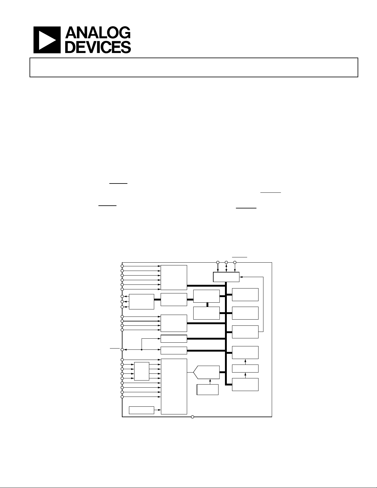
FUNCTIONAL BLOCK DIAGRAM
VID5
VID4
VID3
VID2
VID1
VID0
PWM1
PWM2
PWM3
TACH1
TACH2
TACH3
TACH4
THERM
+12V
+2.5V
Rev. 0
Information furnished by Analog Devices is believed to be accurate and reliable.
However, no responsibility is assumed by Analog Devices for its use, nor for any
infringements of patents or other rights of third parties that may result from its use.
Specifications subject to change without notice. No license is granted by implication
or otherwise under any patent or patent rights of Analog Devices. Trademarks and
registered trademarks are the property of their respective owners.
+5V
V
V
D1+
D1–
D2+
D2–
CCP
CC
IN
IN
IN
PWM REGISTERS
AND
CONTROLLERS
HF & LF
VCCTO ADT7468
SRC
BAND GAP
TEMP SENSOR
ACOUSTIC
ENHANCEMENT
CONTROL
ACOUSTIC
ENHANCEMENT
CONTROL
FAN SPEED
COUNTER
PERFORMANCE
MONITORING
THERMAL
PROTECTION
INPUT
SIGNAL
CONDITIONING
AND
ANALOG
MULTIPLEXER
GND
Figure 1.
SCL
SDA
SMBALERT
SERIAL BUS
INTERFACE
AUTOMATIC
FAN SPEED
CONTROL
DYNAMIC
T
MIN
CONTROL
ADT7468
10-BIT
ADC
BAND GAP
REFERENCE
ADDRESS
POINTER
REGISTER
PWM
CONFIGURATION
REGISTERS
INTERRUPT
MASKING
INTERRUPT
STATUS
REGISTERS
LIMIT
COMPARATORS
VALUE AND
LIMIT
REGISTERS
04499-0-001
One Technology Way, P.O. Box 9106, Norwood, MA 02062-9106, U.S.A.
Tel: 781.329.4700 www.analog.com
Fax: 781.326.8703 © 2004 Analog Devices, Inc. All rights reserved.

ADT7468
TABLE OF CONTENTS
Specifications..................................................................................... 3
Absolute Maximum Ratings............................................................ 5
Thermal Characteristics .............................................................. 5
ESD Caution.................................................................................. 5
Pin Configuration and Function Descriptions............................. 6
Typical Performance Characteristics ............................................. 8
Product Description....................................................................... 10
Status Registers........................................................................... 23
THERM
Timer ........................................................................... 25
Fan Drive Using PWM Control ............................................... 28
Laying Out 2-Wire and 3-Wire Fans....................................... 30
Operating from 3.3 V Standby.................................................. 34
XNOR Tree Test Mode .............................................................. 35
Comparison between ADT7463 and ADT7468..................... 10
How to Set the Functionality of Pin 14 ...................................11
Recommended Implementation............................................... 11
Serial Bus Interface..................................................................... 12
Write Operations ........................................................................ 13
Read Operations ......................................................................... 14
SMBus Timeout.......................................................................... 14
Voltage Measurement Input...................................................... 14
Analog-to-Digital Converter ....................................................14
Input Circuitry ............................................................................ 15
Voltage Measurement Registers................................................ 15
Voltage Limit Registers.............................................................. 15
VID Code Monitoring............................................................... 15
VID Code Input Threshold Voltage......................................... 15
VID Code Change Detect Function ........................................ 16
Power-On Default ...................................................................... 35
Programming the Automatic Fan Speed Control Loop ............ 36
Automatic Fan Control Overview............................................ 36
Step 1: Hardware Configuration.............................................. 37
Recommended Implementation 1 ........................................... 38
Recommended Implementation 2 ........................................... 39
Step 2: Configuring the MUX................................................... 40
Step 3: T
Step 4: PWM
Step 5: PWM
Step 7: T
Step 8: T
Dynamic T
Settings for Thermal Calibration Channels....... 42
MIN
for Each PWM (Fan) Output....................... 43
MIN
for PWM (Fan) Outputs.............................. 43
MAX
for Temperature Channels ............................... 47
THERM
for Temperature Channels .................................. 48
HYST
Control Mode ................................................... 49
MIN
Step 9: Operating Points for Temperature Channels............. 51
Step 10: High and Low Limits for Temperature Channels ... 52
Additional ADC Functions for Voltage Measurements ........16
Temperature Measurement Method ........................................ 18
Series Resistance Cancellation.................................................. 19
Factors Affecting Diode Accuracy ........................................... 19
Additional ADC Functions for Temperature Measurement. 21
Limits, Status Registers, and Interrupts ....................................... 22
Limit Values................................................................................. 22
REVISION HISTORY
Revision 0: Initial Version
Rev. 0 | Page 2 of 80
Step 11: Monitoring
THERM
................................................... 55
Enhancing System Acoustics .................................................... 56
Step 12: Ramp Rate for Acoustic Enhancement..................... 58
Register Tables ................................................................................ 60
ADT7468 Programming Block Diagram.................................... 79
Outline Dimensions....................................................................... 80
Ordering Guide .......................................................................... 80

ADT7468
SPECIFICATIONS
TA = T
All voltages are measured with respect to GND, unless otherwise specified. Typicals are at T
norm. Logic inputs accept input high voltages up to V
logic levels of V
not production tested.
Table 1.
Parameter Min Typ Max Unit Test Conditions/Comments
POWER SUPPLY
20 µA Standby mode
TEMP-TO-DIGITAL CONVERTER
36 µΑ Second current
96 µΑ Third current
ANALOG-TO-DIGITAL CONVERTER (INCLUDING MUX AND ATTENUATORS)
FAN RPM-TO-DIGITAL CONVERTER
MIN
to T
, VCC = V
MAX
= 0.8 V for a falling edge and VIH = 2.0 V for a rising edge. SMBus timing specifications are guaranteed by design and are
IL
MIN
to V
, unless otherwise noted.
MAX
MAX
= 25°C and represent most likely parametric
A
even when device is operating down to V
. Timing specifications are tested at
MIN
Supply Voltage 3.0 3.3 5.5 V
Supply Current, ICC 3 mA Interface inactive, ADC active
Local Sensor Accuracy ±1.5 °C 0°C ≤ TA ≤ 70°C
−3.5 +2 °C −40°C ≤ TA ≤ +100°C
−4 +2 °C −40°C ≤ TA ≤ +120°C
Resolution 0.25 °C
Remote Diode Sensor Accuracy ±1.5 °C 0°C ≤ TA ≤ 70°C; 0°C ≤ TD ≤ 120°C
−3.5 +2 °C −40°C ≤ TA ≤ +100°C; 0°C ≤ TD ≤ +120°C
−4.5 +2 °C −40°C ≤ TA ≤ +120°C; 0°C ≤ TD ≤ +120°C
Resolution 0.25 °C
Remote Sensor Source Current 6 µA First current
Total Unadjusted Error (TUE) ±2 % For 12 V and 5 V channels
±1.5 % For all other channels
Differential Nonlinearity (DNL) ±1 LSB 8 bits
Power Supply Sensitivity ±0.1 %/V
Conversion Time (Voltage Input) 11 ms Averaging enabled
Conversion Time (Local Temperature) 12 ms Averaging enabled
Conversion Time (Remote Temperature) 38 ms Averaging enabled
Total Monitoring Cycle Time 145 ms Averaging enabled
Total Monitoring Cycle Time 19 ms Averaging disabled
Input Resistance 40 70 100 kΩ For V
channel
CC
80 140 200 kΩ For all other channels
Accuracy ±5 % 0°C ≤ TA ≤ 70°C , 3.3 V
±7 % −40°C ≤ TA ≤ +120°C , 3.3 V
±10 % −40°C ≤ TA ≤ +120°C , 5.5 V
Full-Scale Count 65,535
Nominal Input RPM 109 RPM Fan count = 0xBFFF
329 RPM Fan count = 0x3FFF
5000 RPM Fan count = 0x0438
10000 RPM Fan count = 0x021C
Internal Clock Frequency 85.5 90 94.5 kHz 0°C ≤ TA ≤ 70°C, V
83.7 90 96.3 kHz −40°C ≤ TA ≤ +120°C, V
81 90 99 kHz −40°C ≤ TA ≤ +120°C, V
CC
= 3.3 V
CC
CC
= 3.3 V
= 5.5 V
Rev. 0 | Page 3 of 80
ADT7468
A
Parameter Min Typ Max Unit Test Conditions/Comments
OPEN-DRAIN DIGITAL OUTPUTS, PWM1 TO PWM3, XTO
Current Sink, IOL 8.0 mA
Output Low Voltage, VOL 0.4 V I
High Level Output Current, IOH 0.1 1.0 µA V
OPEN-DRAIN SERIAL DATA BUS OUTPUT (SDA)
Output Low Voltage, VOL 0.4 V I
High Level Output Current, IOH 0.1 1.0 µA V
SMBUS DIGITAL INPUTS (SCL, SDA)
Input High Voltage, VIH 2.0 V
Input Low Voltage, V
0.4 V
IL
Hysteresis 500 mV
DIGITAL INPUT LOGIC LEVELS (TACH INPUTS)
Input High Voltage, VIH 2.0 V
5.5 V Maximum input voltage
Input Low Voltage, VIL 0.8 V
−0.3 V Minimum input voltage
Hysteresis 0.5 V p-p
DIGITAL INPUT LOGIC LEVELS (THERM) ADTL+
Input High Voltage, V
Input Low Voltage, V
0.75 × V
IH
0.4 V
IL
V
CCP
DIGITAL INPUT CURRENT
Input High Current, IIH −1 µA VIN = VCC
Input Low Current, IIL 1 µA VIN = 0
Input Capacitance, CIN 5 pF
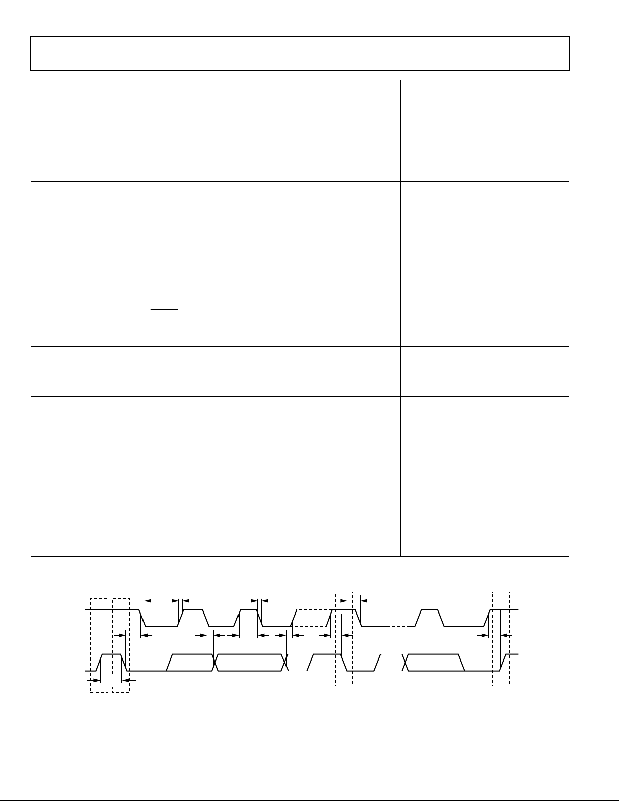
SERIAL BUS TIMING See Figure 2
Clock Frequency, f
10 400 kHz
SCLK
Glitch Immunity, tSW 50 ns
Bus Free Time, t
Start Setup Time, t
Start Hold Time, t
SCL Low Time, t
SCL High Time, t
4.7 µs
BUF
4.7 µs
SU;STA
4.0 µs
HD;STA
4.7 µs
LOW
4.0 50 µs
HIGH
SCL, SDA Rise Time, tR 1000 ns
SCL, SDA Fall Time, t
Data Setup Time, t
Data Hold Time, t
Detect Clock Low Timeout, t
300 µs
F
250 ns
SU;DAT
300 ns
HD;DAT
15 35 ms Can be optionally disabled
TIMEOUT
= −8.0 mA, VCC = +3.3 V
OUT
= VCC
OUT
= −4.0 mA, VCC = +3.3 V
OUT
= VCC
OUT
t
F
t
HIGH
t
SU; DAT
SP
Figure 2. Serial Bus Timing Diagram
t
SU; STA
t
HD; STA
t
SU; STO
04499-0-002
SCL
SD
t
BUF
PS
t
HD; STA
t
LOW
t
R
t
HD; DAT
Rev. 0 | Page 4 of 80

ADT7468
ABSOLUTE MAXIMUM RATINGS
Table 2.
Parameter Rating
Positive Supply Voltage (VCC) 5.5 V
Maximum Voltage on 12 VIN Pin 20 V
Voltage on Any Input or Output Pin −0.3 V to +6.5 V
Input Current at Any Pin ±5 mA
Package Input Current ±20 mA
Maximum Junction Temperature (T
Storage Temperature Range −65°C to +150°C
Lead Temperature, Soldering
IR Reflow Peak Temperature 220°C
Lead Temperature (Soldering 10 s) 300°C
ESD Rating 1000 V
) 150°C
JMAX
ESD CAUTION
ESD (electrostatic discharge) sensitive device. Electrostatic charges as high as 4000 V readily accumulate on
the human body and test equipment and can discharge without detection. Although this product features
proprietary ESD protection circuitry, permanent damage may occur on devices subjected to high energy
electrostatic discharges. Therefore, proper ESD precautions are recommended to avoid performance
degradation or loss of functionality.
Stresses above those listed under Absolute Maximum Ratings
may cause permanent damage to the device. This is a stress
rating only; functional operation of the device at these or any
other conditions above those indicated in the operational
section of this specification is not implied. Exposure to absolute
maximum rating conditions for extended periods may affect
device reliability.
THERMAL CHARACTERISTICS
24-lead QSOP package:
= 150°C/W
θ
JA
= 39°C/W
θ
JC
Rev. 0 | Page 5 of 80
ADT7468
PIN CONFIGURATION AND FUNCTION DESCRIPTIONS
SDA
SCL
GND
V
VID0
VID1
VID2
VID3
TACH3
PWM2/SMBALERT
TACH1
TACH2
1
2
3
4
CC
5
6
7
8
9
10
11
12
ADT7468
TOP VIEW
(NOT TO SCALE)
PWM1/XTO
24
V
23
CCP
+2.5V
22
IN
21
+12VIN/VID5
/THERM
+5V
20
IN
VID4
19
D1+
18
17
D1–
16
D2+
15
D2–
14
TACH4/GPIO/THERM/SMBALERT
13
PWM3
04499-0-003
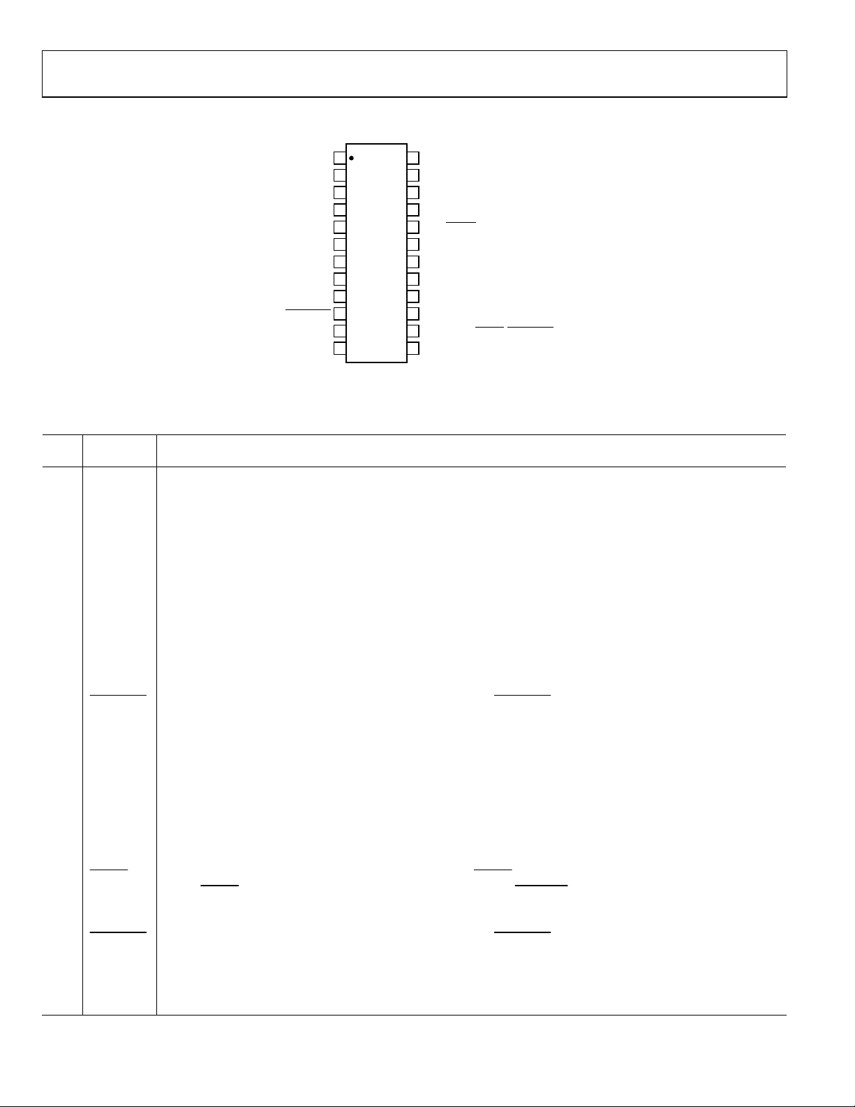
Figure 3. Pin Configuration
Table 3. Pin Function Descriptions
Pin
No.
Mnemonic Description
1 SDA Digital I/O (Open Drain). SMBus bidirectional serial data. Requires pull-up resistor.
2 SCL Digital Input (Open Drain). SMBus serial clock input. Requires pull-up resistor.
3 GND Ground Pin.
4 VCC
Power Supply. Can be powered by 3.3 V standby, if monitoring in low power states is required. V
is also monitored
CC
through this pin. The ADT7468 can also be powered from a 5 V supply. Setting Bit 7 of Configuration Register 1
(Reg. 0x40) rescales the V
input attenuators to correctly measure a 5 V supply.
CC
5 VID0 Digital Input (Open Drain). Voltage supply readouts from CPU. This value is read into the VID register (Reg. 0x43).
6 VID1 Digital Input (Open Drain). Voltage supply readouts from CPU. This value is read into the VID register (Reg. 0x43).
7 VID2 Digital Input (Open Drain). Voltage supply readouts from CPU. This value is read into the VID register (Reg. 0x43).
8 VID3 Digital Input (Open Drain). Voltage supply readouts from CPU. This value is read into the VID register (Reg. 0x43).
9 TACH3
Digital Input (Open Drain). Fan tachometer input to measure speed of Fan 3. Can be reconfigured as an analog input
(AIN3) to measure the speed of 2-wire fans.
10 PWM2
Digital Output (Open Drain). Requires 10 kΩ typical pull-up. Pulse width modulated output to control Fan 2 speed.
Can be configured as a high or low frequency drive.
SMBALERT
Digital Output (Open Drain). This pin can be reconfigured as an SMBALERT interrupt output to signal out-of-limit
conditions.
11 TACH1
Digital Input (Open Drain). Fan tachometer input to measure speed of Fan 1. Can be reconfigured as an analog input
(AIN1) to measure the speed of 2-wire fans.
12 TACH2
Digital Input (Open Drain). Fan tachometer input to measure speed of Fan 2. Can be reconfigured as an analog input
(AIN2) to measure the speed of 2-wire fans.
13 PWM3
Digital I/O (Open Drain). Pulse width modulated output to control speed of Fan 3 and Fan 4. Requires 10 kΩ typical
pull-up. Can be configured as a high or low frequency drive.
14 TACH4
Digital Input (Open Drain). Fan tachometer input to measure speed of Fan 4. Can be reconfigured as an analog input
(AIN4) to measure the speed of 2-wire fans.
GPIO General Purpose Open Drain Digital I/O.
Alternatively, the pin can be reconfigured as a bidirectional THERM pin. Can be used to time and monitor assertions
THERM
on the THERM
input. For example, this pin can be connected to the PROCHOT output of an Intel Pentium 4 processor
or to the output of a trip point temperature sensor. This pin can also be used as an output to signal overtemperature
conditions.
SMBALERT
Digital Output (Open Drain). This pin can be reconfigured as an SMBALERT interrupt output to signal out-of-limit
conditions.
15 D2– Cathode Connection to Second Thermal Diode.
16 D2+ Anode Connection to Second Thermal Diode.
17 D1– Cathode Connection to First Thermal Diode.
Rev. 0 | Page 6 of 80

ADT7468
Pin
No. Mnemonic Description
18 D1+ Anode Connection to First Thermal Diode.
19 VID4 Digital Input (Open Drain). Voltage supply readouts from CPU. This value is read into the VID register (Reg. 0x43).
20 +5VIN Analog Input. Monitors +5 V power supply.
21 +12VIN Analog Input. Monitors +12 V power supply.
VID5
22 +2.5VIN Analog Input. Monitors +2.5 V supply, typically a chipset voltage.
23 V
24 PWM1 Digital Output (Open Drain). Pulse width modulated output to control Fan 1 speed. Requires 10 kΩ typical pull-up.
XTO Also functions as the output from the XOR tree in XOR test mode.
Alternatively, this pin can be reconfigured as a bidirectional THERM pin. Can be used to time and monitor assertions
THERM
on the THERM
the output of a trip point temperature sensor. This pin can also be used as an output to signal overtemperature
conditions.
Digital Input (Open Drain). Voltage supply readouts from CPU. This value is read into the VID register (Reg. 0x43).
Supports VRM10 solutions.
Analog Input. Monitors processor core voltage (0 V to 3 V).
CCP
input. For example, it can be connected to the PROCHOT output of an Intel Pentium 4 processor or to
Rev. 0 | Page 7 of 80
ADT7468
TYPICAL PERFORMANCE CHARACTERISTICS
0
20
100mV
–10
–20
–30
–40
TEMPERATURE ERROR (°C)
–50
–60
1 4.73.3 100 2.2
CAPACITANCE (nF)
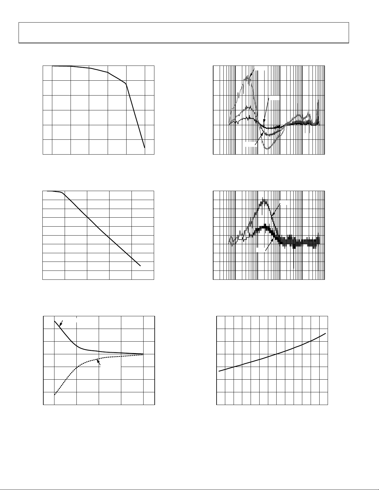
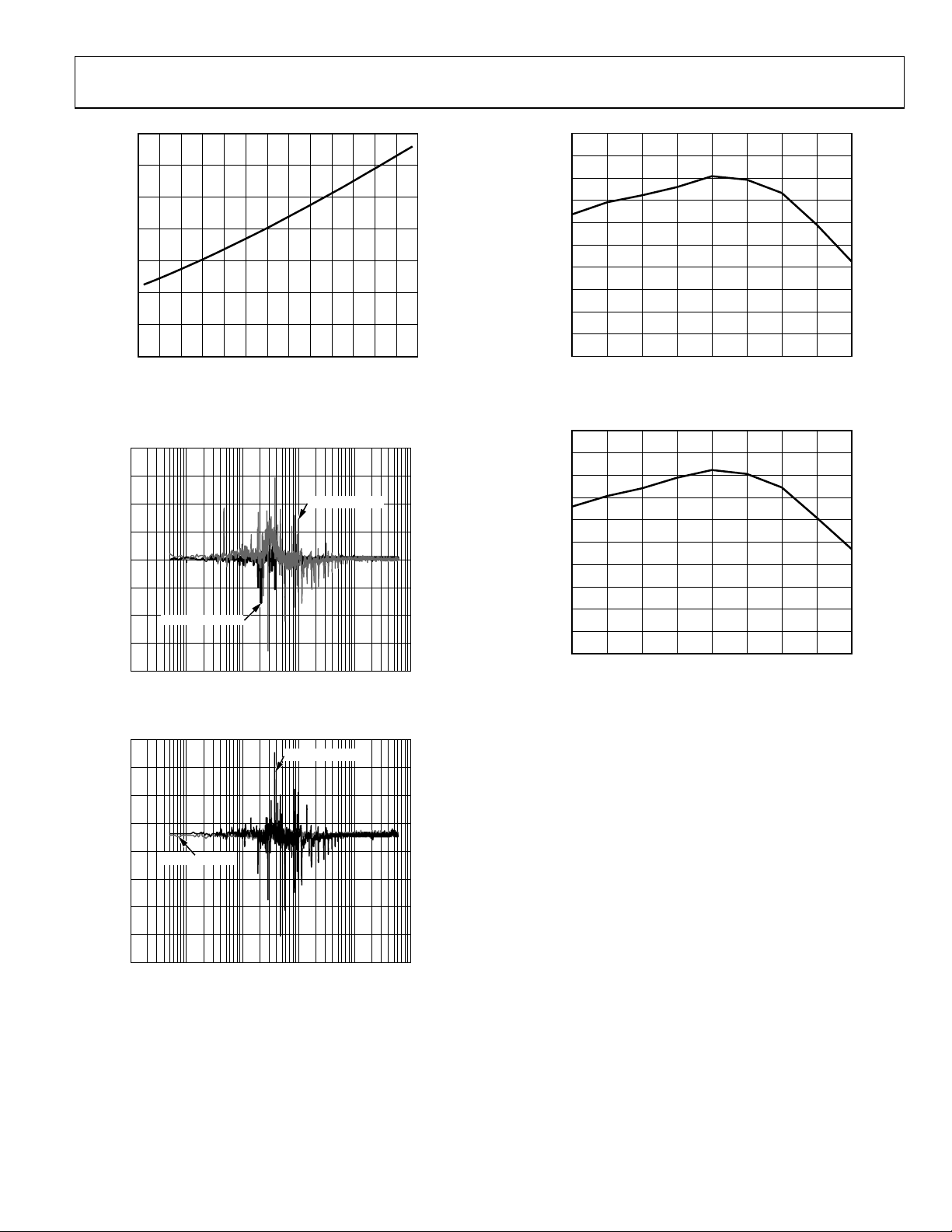
Figure 4. Temperature Error vs. Capacitance between D+ and D−
0
–10
–20
–30
–40
–50
–60
–70
TEMPERATURE ERROR (°C)
–80
–90
–100
CAPACITANCE (nF)
Figure 5. External Temperature Error vs. D+/D− Capacitance
60
40
D+ TO GND
15
04499-0-045
10
5
0
TEMPERATURE ERROR (°C)
–5
–10
60mV
40mV
FREQUENCY (kHz)
1G10 100 1M 10M 100M
04499-0-048
Figure 7. Remote Temperature Error vs. Common Mode Noise Frequency
6
5
4
3
2
1
0
–1
TEMPERATURE ERROR (°C)
–2
–3
2501020515
04499-0-046
–4
10mV
FREQUENCY (kHz)
20mV
1G10 100 1M 10M 100M
04499-0-049
Figure 8. Remote Temperature Error vs. Differential Mode Noise Frequency
1.40
1.35
20
0
D+ TO V
–20
–40
TEMPERATURE ERROR (°C)
–60
–80
RESISTANCE (MΩ)
CC
Figure 6. Remote Temperature Error vs. PCB Resistance
1.30
1.25
(mA)
1.20
DD
I
1.15
1.10
1000 3.3 20110
04499-0-047
1.05
3.0 3.8 5.23.4 4.43.6 4.83.2 4.0 5.44.6 5.04.2
POWER SUPPLY VOLTAGE (V)
Figure 9. Normal I
vs. Power Supply
DD
04499-0-050
Rev. 0 | Page 8 of 80
ADT7468
7
6
5
4
A)
µ
(
3
DD
I
2
1
0
3.0 3.8 5.23.4 4.43.6 4.83.2 4.0 5.44.6 5.04.2
POWER SUPPLY VOLTAGE (V)
Figure 10. Shutdown I
vs. Power Supply
DD
20
15
10
5
0
–5
–10
TEMPERATURE ERROR (°C)
–15
–20
INT ERROR, 100mV
POWER SUPPLY NOISE FREQUENCY (kHz)
INT ERROR, 250mV
Figure 11. Internal Temperature Error vs. Power Supply
20
15
EXT ERROR, 250mV
04499-0-051
1G10 100 1M 10M 100M
04499-0-052
1.0
0.5
0
–0.5
–1.0
–1.5
–2.0
ERROR (°C)
–2.5
–3.0
–3.5
–4.0
TEMPERATURE (°C)
Figure 13. Internal Temperature Error vs. ADT7468 Temperature
1.0
0.5
0
–0.5
–1.0
–1.5
–2.0
ERROR (°C)
–2.5
–3.0
–3.5
–4.0
TEMPERATURE (°C)
Figure 14. Remote Temperature Error vs. ADT7468 Temperature
120–40 –20 0 20 40 60 80 100
04499-0-091
120–40 –20 0 20 40 60 80 100
04499-0-092
10
5
0
EXT ERROR, 100mV
–5
–10
TEMPERATURE ERROR (°C)
–15
–20
POWER SUPPLY NOISE FREQUENCY (kHz)
1G10 100 1M 10M 100M
Figure 12. Remote Temperature Error vs. Power Supply Noise Frequency
04499-0-053
Rev. 0 | Page 9 of 80

ADT7468
PRODUCT DESCRIPTION
The ADT7468 is a complete thermal monitor and multiple fan
controller for any system requiring thermal monitoring and
cooling. The device communicates with the system via a serial
system management bus. The serial bus controller has a serial
data line for reading and writing addresses and data (Pin 1), and
an input line for the serial clock (Pin 2). All control and
programming functions for the ADT7468 are performed over
the serial bus. In addition, a pin can be reconfigured as an
SMBALERT
COMPARISON BETWEEN ADT7463 AND ADT7468
The ADT7468 is an upgrade to the ADT7463. The ADT7468
and ADT7463 are almost pin and register map compatible. The
ADT7468 and ADT7463 have the following differences:
1. On the ADT7468, the PWM drive signals can be config-
2. Once the V
3. The fans are switched off by default on power-up on the
4. Series resistance cancellation (SRC) is provided on the
output to signal out-of-limit conditions.
ured as either high frequency or low frequency drives. The
low frequency option is programmable between 10 Hz and
100 Hz. The high frequency option is 22.5 kHz. On the
ADT7463, only the low frequency option is available.
is powered up, monitoring of temperature
CC
and fan speeds is enabled on the ADT7468 when V
powered up, or if V
is never powered up, when the first
CCP
CCP
is
SMBus transaction with the ADT7468 is completed. On the
ADT7463, the STRT bit in Configuration Register 1 must
be set to enable monitoring.
ADT7468. On the ADT7463, the fans run at full speed on
power-up.
Fail-safe cooling is provided on the ADT7468 in that, if the
measured temperature exceeds the
THERM
limit (100°C),
the fans run at full speed.
Fail-safe cooling is also provided 4.6 s after V
is powered
CCP
up. See Figure 48. The fans go to full speed, if the ADT7468
has not been addressed via the SMBus within 4.6 s of when
the V
is powered up. This protects the system in the
CCP
event that the SMBus fails. The ADT7468 can be programmed at any time, either before or after the 4.6 s has
elapsed, and it behaves as programmed. If V
powered up, fail-safe cooling is effectively disabled. If V
is never
CCP
CCP
is disabled, writing to the ADT7468 at any time causes the
ADT7468 to operate normally.
remote temperature channels on the ADT7468, but not on
the ADT7463. SRC automatically cancels linear offset
introduced by a series resistance between the thermal
diode and the sensor.
5. The ADT7468 has an extended temperature measurement
range. The measurement range goes from–64°C to +191°C.
On the ADT7463, the measurement range is from −127°C
to +127°C. This means that the ADT7468 can measure
higher temperatures. The ADT7468 also includes the
ADT7463 temperature range; the temperature measurement range can be switched by setting Bit 0 of
Configuration Register 5.
6. The ADT7468 maximum fan speed (% duty cycle) in the
automatic fan speed control loop can be programmed. The
maximum fan speed is 100% duty cycle on the ADT7463
and is not programmable.
7. The offset register in the ADT7468 is programmable up to
±64°C with 0.50°C resolution. The offset register of the
ADT7463 is programmable up to ±32°C with 0.25°C
resolution.
8. V
is monitored on Pin 23 of the ADT7468 and can be
CCP
used to set the threshold for
). The threshold for
V
CCP
= 1.7 V and VIL = 0.8 V on the ADT7463.
V
IH
THERM
THERM (PROCHOT
PROCHOT
(
) (2/3 of
) is set at
9. On the ADT7463, Pin 22 can be reconfigured as SMBus
ALERT. This is not available on the ADT7468; instead,
SMBALERT
can be enabled on Pin 14.
10. A GPIO can also be made available on Pin 14 on the
ADT7468. This is not available on the ADT7463. Set the
GPIO polarity and direction in Configuration Register 5.
The GPIO status bit is Bit 5 of Status Register 2 (shared
with TACH4 and
THERM
, because only one can be
enabled at a time).
11. The ADT7463 has three possible SMBus addresses, which
are selectable using the address select and address enable
pins. The ADT7468 has one SMBus address available at
Address 0x2E.
Due to the inclusion of extra functionality, the register map has
changed, including an additional configuration register:
Configuration Register 5 at Address 0x7C.
Configuration Register 5
Bit 0: If Bit 0 is set to 1, the ADT7468 is backward compatible
temperature-wise with the ADT7463. Measurements, T
MIN
calibration circuit, fan control, etc., work in the range −127°C to
+127°C. Also, care should be taken in reprogramming the
temperature limits (T
, operating point,
MIN
THERM
limits) to
their desired twos complement value, because the power-on
default for them is at Offset 64. The extended temperature range
is −64°C to 191°C. The default is 1, which is in the −64°C to
+191°C temperature range.
Rev. 0 | Page 10 of 80
ADT7468
Bit 1= 0 is the high frequency (22.5 kHz) fan drive signal.
Bit 1 = 1 switches the fan drive to low frequency PWM,
programmable between 10 Hz and 100 Hz, the same as the
ADT7463. The default = 0 = HF PWM.
Bit 2 sets the direction for the GPIO: 0 = input, 1 = output.
RECOMMENDED IMPLEMENTATION
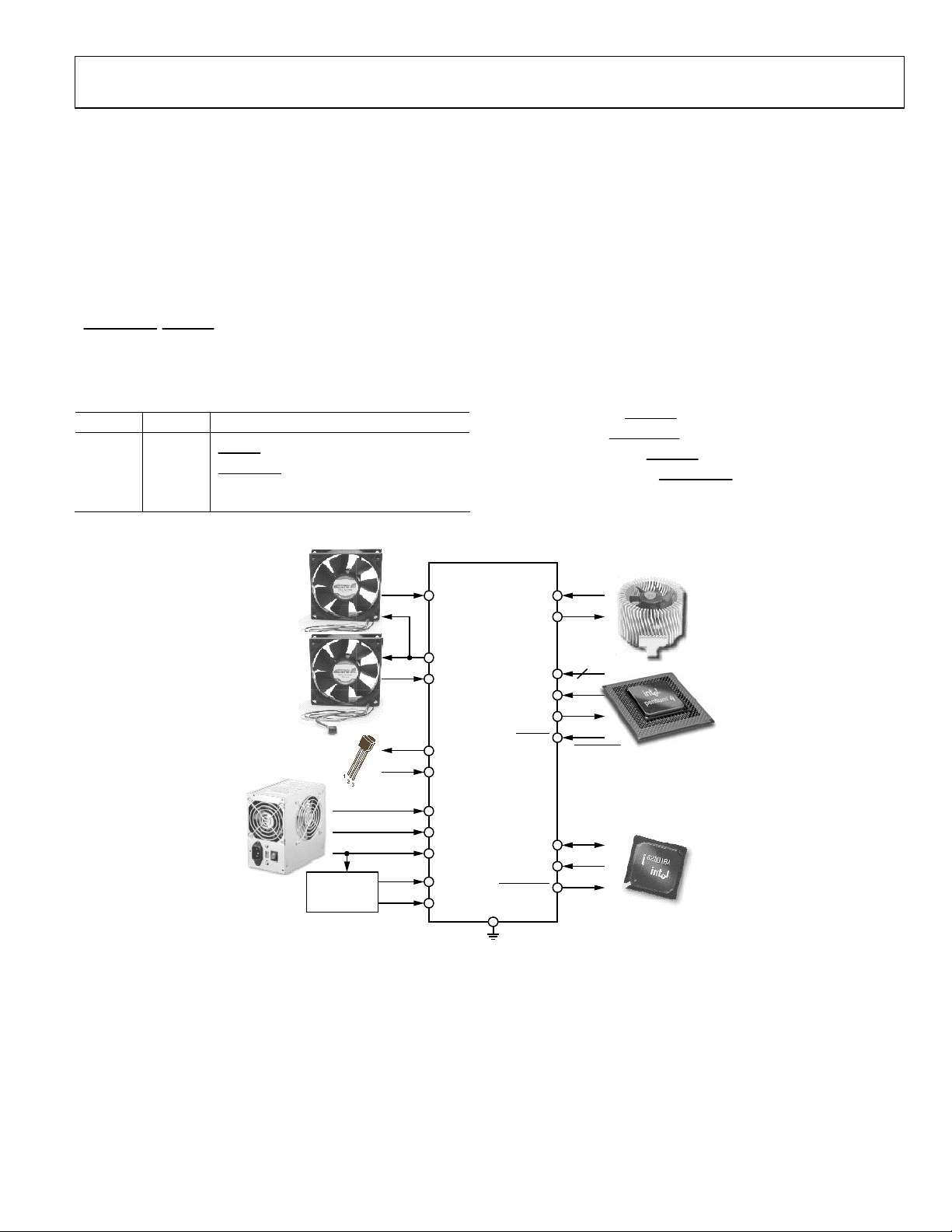
Configuring the ADT7468 as in Figure 15 allows the system
designer to use the following features:
• Two PWM outputs for fan control of up to three fans (the
front and rear chassis fans are connected in parallel).
Bit 3 sets the GPIO polarity: 0 = active low, 1 = active high.
HOW TO SET THE FUNCTIONALITY OF PIN 14
Pin 14 on the ADT7468 has four possible functions:
SMBALERT
required functionality by setting Bit 0 and Bit 1 of Configuration Register 4 at Address 0x7D.
Table 4. Pin 14 Settings
Bit 0 Bit 1 Function
00 TACH4
01
10
11 GPIO
THERM
,
, GPIO, and TACH4. The user chooses the
THERM
SMBALERT
FRONT
CHASSIS
FAN
REAR
CHASSIS
FAN
AMBIENT
TEMPERATURE
TACH2
PWM3
TACH3
D1+
D1–
• Three TACH fan speed measurement inputs.
• V
• CPU temperature measured using Remote 1 temperature
• Ambient temperature measured through Remote 2
• Bidirectional
ADT7468
VID[0:4]/VID[0:5]
THERM
measured internally through Pin 3.
CC
channel.
temperature channel.
Pentium 4
overtemperature
programmed as an
PWM1
TACH1
5(VRM9)/6(VRM10)
D2+
D2–
PROCHOT
THERM
PROCHOT
THERM
SMBALERT
CPU FAN
CPU
pin. This feature allows Intel
monitoring and can function as an
output. It can alternatively be
system interrupt output.
3.3VSB
ADP316x
VRM
CONTROLLER
V
COMP
5V
12V/VID5
CURRENT
V
CORE
GND
SDA
SCL
SMBALERT
ICH
04499-0-004
Figure 15. ADT7468 Configuration
Rev. 0 | Page 11 of 80
ADT7468
SERIAL BUS INTERFACE
On PCs and servers, control of the ADT7468 is carried out
using the serial system management bus (SMBus). The
ADT7468 is connected to this bus as a slave device, under the
control of a master controller, which is usually (but not
necessarily) the ICH.
The ADT7468 has a fixed 7-bit serial bus address of 0101110 or
0x2E. The read/write bit must be added to get the 8-bit address
(01011100 or 0x5C). Data is sent over the serial bus in
sequences of nine clock pulses: eight bits of data followed by an
acknowledge bit from the slave device. Transitions on the data
line must occur during the low period of the clock signal and
remain stable during the high period, because a low-to-high
transition when the clock is high might be interpreted as a stop
signal. The number of data bytes that can be transmitted over
the serial bus in a single read or write operation is limited only
by what the master and slave devices can handle.
When all data bytes have been read or written, stop conditions
are established. In write mode, the master pulls the data line
high during the tenth clock pulse to assert a stop condition. In
read mode, the master device overrides the acknowledge bit by
pulling the data line high during the low period before the
ninth clock pulse. This is known as No Acknowledge. The
master then takes the data line low during the low period before
the tenth clock pulse, and then high during the tenth clock
pulse to assert a stop condition.
Any number of bytes of data can be transferred over the serial
bus in one operation, but it is not possible to mix read and write
in one operation, because the type of operation is determined at
the beginning and cannot subsequently be changed without
starting a new operation.
In the ADT7468, write operations contain either one or two
bytes, and read operations contain one byte and perform the
following functions. To write data to one of the device data
registers or read data from it, the address pointer register must
be set so that the correct data register is addressed, then data
can be written into that register or read from it. The first byte of
a write operation always contains an address that is stored in the
address pointer register. If data is to be written to the device,
then the write operation contains a second data byte that is
written to the register selected by the address pointer register.
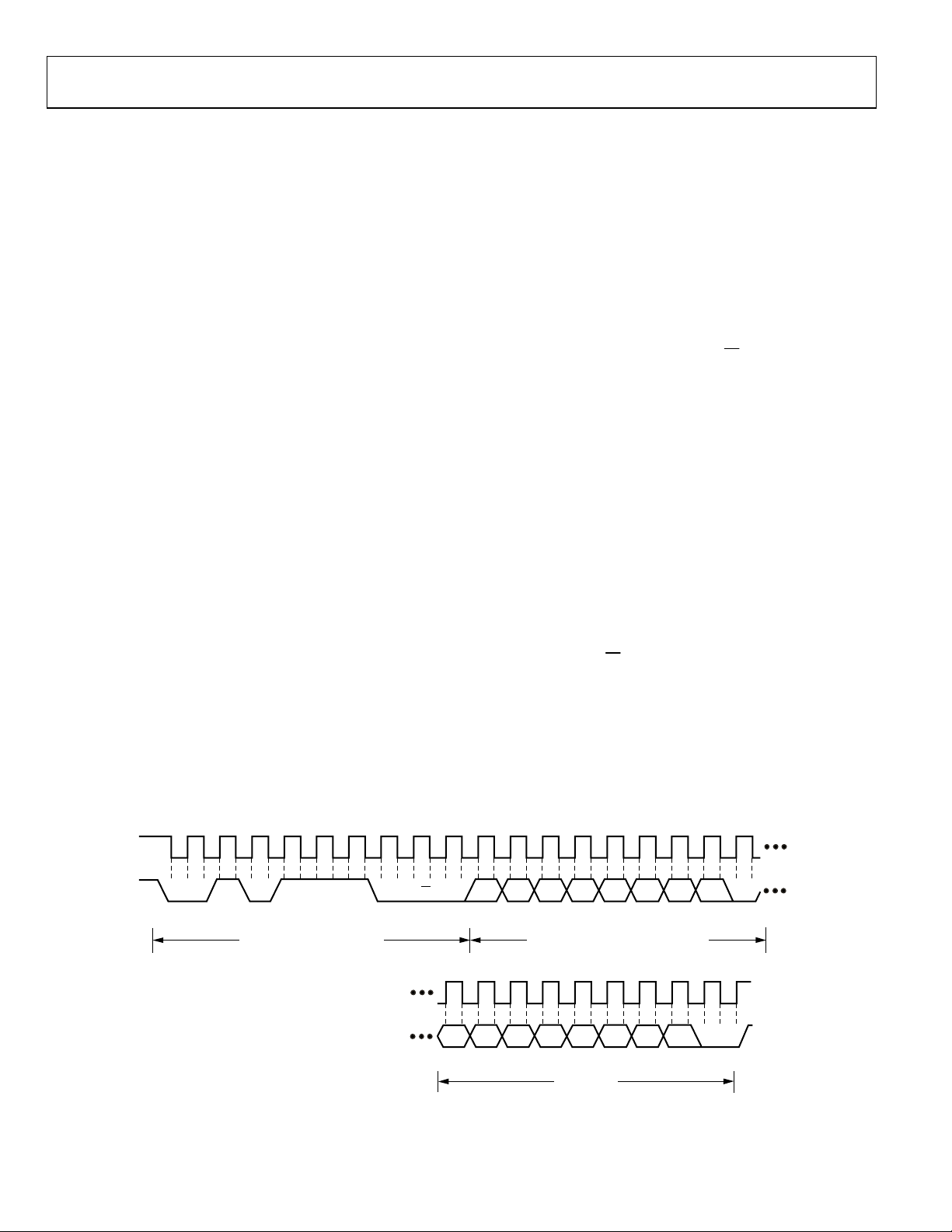
This write operation is illustrated in Figure 16. The device
W
address is sent over the bus, and then R/
is set to 0. This is
followed by two data bytes. The first data byte is the address of
the internal data register to be written to, which is stored in the
address pointer register. The second data byte is the data to be
written to the internal data register.
When reading data from a register, there are two possibilities:
• If the ADT7468’s address pointer register value is unknown
or not the desired value, it must first be set to the correct
value before data can be read from the desired data register.
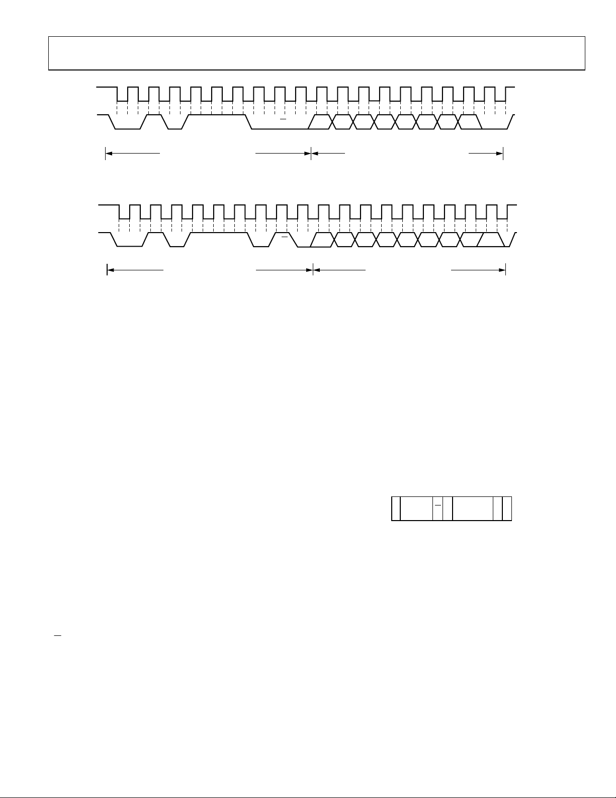
This is done by performing a write to the ADT7468 as
before, but only the data byte containing the register
address is sent, because no data is written to the register.
This is shown in Figure 17.
A read operation is then performed consisting of the serial
W
bus address, R/
bit set to 1, followed by the data byte read
from the data register. This is shown in Figure 18.
• If the address pointer register is known to be already at the
desired address, data can be read from the corresponding
data register without first writing to the address pointer
register, as shown in Figure 18.
SCL
SDA
START BY
MASTER
19
0
1011
FRAME 1
SERIAL BUS ADDRESS BYTE
SCL (CONTINUED)
SDA (CONTINUED)
Figure 16. Writing a Register Address to the Address Pointer Register, then Writing Data to the Selected Register
0
1
R/W
ACK. BY
ADT7468
Rev. 0 | Page 12 of 80
1
D6
D7
1
D7
D5
D6
D4
D5
ADDRESS POINTER REGISTER BYTE
D4
D3
FRAME 3
DATA BYTE
D3
FRAME 2
D2
D2
D1
D0
9
D1
D0
ACK. BY
ADT7468
9
ACK. BY
ADT7468
STOP BY
MASTER
04499-0-005
ADT7468
SDA
SCL
SDA
START BY
MASTER
1
0
1011
SERIAL BUS ADDRESS BYTE
FRAME 1
0
1
R/W
ACK. BY
ADT7468
Figure 17. Writing to the Address Pointer Register Only
1
SCL
0
START BY
MASTER
10
SERIAL BUS ADDRESS BYTE
1
FRAME 1
1
0
1
R/W
ACK. BY
ADT7468
Figure 18. Reading Data from a Previously Selected Register
It is possible to read a data byte from a data register without
first writing to the address pointer register, if the address
pointer register is already at the correct value. However, it is not
possible to write data to a register without writing to the address
pointer register, because the first data byte of a write is always
written to the address pointer register.
In addition to supporting the send byte and receive byte
protocols, the ADT7468 also supports the read byte protocol.
(see System Management Bus Specifications Rev. 2 for more
information. This document is available from Intel.)
If several read or write operations must be performed in
succession, the master can send a repeat start condition instead
of a stop condition to begin a new operation.
WRITE OPERATIONS
The SMBus specification defines several protocols for different
types of read and write operations. The ones used in the
ADT7468 are discussed below. The following abbreviations are
used in the diagrams:
S – START
P – STOP
R – READ
W – WRITE
A – ACKNOWLEDGE
A
– NO ACKNOWLEDGE
D0
9
ACK. BY
ADT7468
STOP BY
MASTER
19
D6
D7
D4
D5
ADDRESS POINTER REGISTER BYTE
D3
FRAME 2
D2
D1
19
D6
D7
D4
D5
DATA BYTE FROM ADT7468
D3
FRAME 2
D2
D1
9
D0
NO ACK. BY
MASTER
STOP BY
MASTER
2. The master sends the 7-bit slave address followed by the
write bit (low).
3. The addressed slave device asserts ACK on SDA.
4. The master sends a command code.
5. The slave asserts ACK on SDA.
6. The master asserts a stop condition on SDA and the
transaction ends.
For the ADT7468, the send byte protocol is used to write a
register address to RAM for a subsequent single byte read from
the same address. This operation is illustrated in Figure 19.
231564
SLAVE
ADDRESS
REGISTER
WASAP
ADDRESS
04499-0-008
Figure 19. Setting a Register Address for Subsequent Read
If the master is required to read data from the register
immediately after setting up the address, it can assert a repeat
start condition immediately after the final ACK and carry out a
single byte read without asserting an intermediate stop
condition.
Write Byte
In this operation, the master device sends a command byte and
one data byte to the slave device, as follows:
04499-0-006
04499-0-007
The ADT7468 uses the following SMBus write protocols.
Send Byte
In this operation, the master device sends a single command
byte to a slave device as follows:
1. The master device asserts a start condition on SDA.
1. The master device asserts a start condition on SDA.
2. The master sends the 7-bit slave address followed by the
write bit (low).
3. The addressed slave device asserts ACK on SDA.
4. The master sends a command code.
Rev. 0 | Page 13 of 80

ADT7468
5. The slave asserts ACK on SDA.
SMBALERT
1.
is pulled low.
6. The master sends a data byte.
7. The slave asserts ACK on SDA.
8. The master asserts a stop condition on SDA to end the
transaction.
This operation is illustrated in Figure 20.
24653178
SLAVE
ADDRESS
Figure 20. Single Byte Write to a Register
SLAVE
ADDRESS
DATAAAWSAP
04499-0-009
READ OPERATIONS
The ADT7468 uses the following SMBus read protocols.
Receive Byte
This operation is useful when repeatedly reading a single
register. The register address must have been set up previously.
In this operation, the master device receives a single byte from a
slave device as follows:
1. The master device asserts a start condition on SDA.
2. The master sends the 7-bit slave address followed by the
read bit (high).
3. The addressed slave device asserts ACK on SDA.
4. The master receives a data byte.
5. The master asserts NO ACK on SDA.
6. The master asserts a stop condition on SDA and the
transaction ends.
In the ADT7468, the receive byte protocol is used to read a
single byte of data from a register whose address has previously
been set by a send byte or write byte operation. This operation
is illustrated in Figure 21.
213564
SLAVE
SRAAPDATA
ADDRESS
Figure 21. Single Byte Read from a Register
Alert Response Address
Alert response address (ARA) is a feature of SMBus devices that
allows an interrupting device to identify itself to the host when
multiple devices exist on the same bus.
SMBALERT
The
output or an
connected to a common
master. If a device’s
output can be used as either an interrupt
SMBALERT
. One or more outputs can be
SMBALERT
SMBALERT
line connected to the
line goes low, the following
procedure occurs:
04499-0-010
2. The master initiates a read operation and sends the alert
response address (ARA = 0001 100). This is a general call
address that must not be used as a specific device address.
3. The device whose
SMBALERT
output is low responds to
the alert response address, and the master reads its device
address. The address of the device is now known and can
be interrogated in the usual way.
4. If more than one device’s
SMBALERT
output is low, the
one with the lowest device address has priority in accordance with normal SMBus arbitration.
5. Once the ADT7468 has responded to the alert response
address, the master must read the status registers and the
SMBALERT
is cleared only if the error condition has gone
away.
SMBUS TIMEOUT
The ADT7468 includes an SMBus timeout feature. If there is no
SMBus activity for 35 ms, the ADT7468 assumes that the bus is
locked and releases the bus. This prevents the device from
locking or holding the SMBus expecting data. Some SMBus
controllers cannot handle the SMBus timeout feature, so it can
be disabled.
Configuration Register 1(Reg. 0x40)
<6> TODIS = 0, SMBus timeout enabled (default).
<6> TODIS = 1, SMBus timeout disabled.
VOLTAGE MEASUREMENT INPUT
The ADT7468 has four external voltage measurement channels.
It can also measure its own supply voltage, V
. Pins 20 to 23
CC
can measure 5 V, 12 V, and 2.5 V supplies, and the processor
core voltage V
measurement is carried out through the V
(0 V to 3 V input). The VCC supply voltage
CCP
pin (Pin 4). Setting
CC
Bit 7 of Configuration Register 1 (Reg. 0x40) allows a 5 V
supply to power the ADT7468 and be measured without
overranging the V
measurement channel. The 2.5 V input can
CC
be used to monitor a chipset supply voltage in computer
systems.
ANALOG-TO-DIGITAL CONVERTER
All analog inputs are multiplexed into the on-chip, successiveapproximation, analog-to-digital converter. This has a resolution of 10 bits. The basic input range is 0 V to 2.25 V, but the
inputs have built-in attenuators to allow measurement of 2.5 V,
3.3 V, 5 V, 12 V, and the processor core voltage V
external components. To allow for the tolerance of these supply
voltages, the ADC produces an output of 3/4 full scale (decimal
768 or 300 hex) for the nominal input voltage and so has
adequate headroom to cope with overvoltages.
without any
CCP
Rev. 0 | Page 14 of 80
ADT7468
INPUT CIRCUITRY
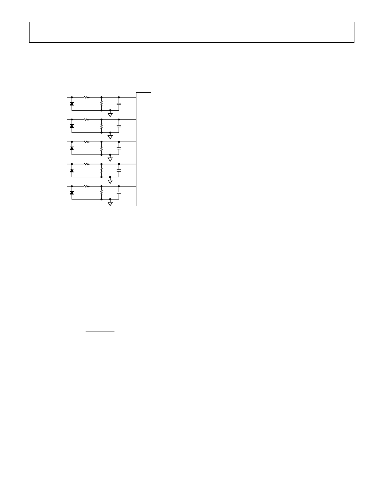
The internal structure for the analog inputs is shown in
Figure 22. The input circuit consists of an input protection
diode, an attenuator, plus a capacitor to form a first-order lowpass filter that gives input immunity to high frequency noise.
12V
3.3V
2.5V
V
5V
CCP
120kΩ
IN
IN
IN
IN
Figure 22. Structure of Analog Inputs
20kΩ 30pF
93kΩ
47kΩ 30pF
68kΩ
71kΩ 30pF
45kΩ
94kΩ 30pF
17.5kΩ
52.5kΩ 35pF
MUX
04499-0-011
Reg. 0x4C, 12 V Low Limit = 0x00 default
Reg. 0x4D, 12 V High Limit = 0xFF default
Table 5 shows the input ranges of the analog inputs and output
codes of the 10-bit ADC.
When the ADC is running, it samples and converts a voltage
input in 0.7 ms and averages 16 conversions to reduce noise; a
measurement takes nominally 11 ms.
VID CODE MONITORING
The ADT7468 has five dedicated voltage ID (VID code)
inputs. These are digital inputs that can be read back through
the VID register (Reg. 0x43) to determine the processor voltage
required or being used in the system. Five VID code inputs
support VRM9.x solutions. In addition, Pin 21 (12 V input) can
be reconfigured as a sixth VID input to satisfy future VRM
requirements.
VID Code Register (Reg. 0x43)
<0> = VID0, reflects logic state of Pin 5.
<1> = VID1, reflects logic state of Pin 6.
<2> = VID2, reflects logic state of Pin 7.
VOLTAGE MEASUREMENT REGISTERS
Reg. 0x20, 2.5 V Reading = 0x00 default
Reg. 0x21, V
Reg. 0x22, V
Reading = 0x00 default
CCP
Reading = 0x00 default
CC
Reg. 0x23, 5 V Reading = 0x00 default
Reg. 0x24, 12 V Reading = 0x00 default
VOLTAGE LIMIT REGISTERS
Associated with each voltage measurement channel is a high
and low limit register. Exceeding the programmed high or low
limit causes the appropriate status bit to be set. Exceeding either
limit can also generate
SMBALERT
Reg. 0x44, 2.5 V Low Limit = 0x00 default
Reg. 0x45, 2.5 V High Limit = 0xFF default
Reg. 0x46, V
Reg. 0x47, V
Reg. 0x48, V
Reg. 0x49, V
Low Limit = 0x00 default
CCP
High Limit = 0xFF default
CCP
Low Limit = 0x00 default
CC
High Limit = 0xFF default
CC
Reg. 0x4A, 5 V Low Limit = 0x00 default
Reg. 0x4B, 5 V High Limit = 0xFF default
interrupts.
<3> = VID3, reflects logic state of Pin 8.
<4> = VID4, reflects logic state of Pin 19.
<5> = VID5, reconfigurable 12 V input. This bit reads 0 when
Pin 21 is configured as the 12 V input. This bit reflects the logic
state of Pin 21 when the pin is configured as VID5.
VID CODE INPUT THRESHOLD VOLTAGE
The switching threshold for the VID code inputs is approximately 1 V. To enable future compatibility, it is possible to
reduce the VID code input threshold to 0.6 V. Bit 6 (THLD) of
the VID register (Reg. 0x43) controls the VID input threshold
voltage.
VID CODE REGISTER (Reg. 0x43)
<6> THLD = 0, VID switching threshold = 1 V,
< 0.8 V, VIH > 1.7 V, V
V
OL
THLD = 1, VID switching threshold = 0.6 V,
< 0.4 V, VIH > 0.8 V, V
V
OL
Reconfiguring Pin 21 as VID5 Input
Pin 21 can be reconfigured as a sixth VID code input (VID5)
for VRM10 compatible systems. Because the pin is configured
as VID5, it is not possible to monitor a 12 V supply.
Bit 7 of the VID register (Reg. 0x43) determines the function of
Pin 21. System or BIOS software can read the state of Bit 7 to
determine whether the system is designed to monitor 12 V or is
monitoring a sixth VID input.
MAX
MAX
= 3.3 V
= 3.3 V
Rev. 0 | Page 15 of 80

ADT7468
VID Code Register (Reg. 0x43)
<7> VIDSEL = 0, Pin 21 functions as a 12 V measurement
input. Software can read this bit to determine that there are five
VID inputs being monitored. Bit 5 of Register 0x43 (VID5)
always reads back 0. Bit 0 of Status Register 2 (Reg. 0x42)
reflects 12 V out-of-limit measurements.
VIDSEL = 1, Pin 21 functions as the sixth VID code input
(VID5). Software can read this bit to determine that there are
six VID inputs being monitored. Bit 5 of Register 0x43 reflects
the logic state of Pin 21. Bit 0 of Status Register 2 (Reg. 0x42)
reflects VID code changes.
VID CODE CHANGE DETECT FUNCTION
The ADT7468 has a VID code change detect function. When
Pin 21 is configured as the VID5 input, VID code changes can
be detected and reported back by the ADT7468. Bit 0 of Status
Register 2 (Reg. 0x42) is the 12 V/VC bit and denotes a VID
change when set. The VID code change bit is set when the logic
states on the VID inputs are different than they were 11 µs
previously. The change of VID code can be used to generate an
SMBALERT
interrupt. If an
required, Bit 0 of Interrupt Mask Register 2 (Reg. 0x75), when
set, prevents
SMBALERT
changes.
Status Register 2 (Reg. 0x42)
<0> 12V/VC = 0, if Pin 21 is configured as VID5, then Logic 0
denotes no change in VID code within the last 11 µs.
<0> 12V/VC = 1, if Pin 21 is configured as VID5, then Logic 1
means that a change has occurred on the VID code inputs
within the last 11 µs. An
function is enabled.
ADDITIONAL ADC FUNCTIONS FOR VOLTAGE MEASUREMENTS
A number of other functions are available on the ADT7468 to
offer the system designer increased flexibility.
Turn-Off Averaging
For each voltage measurement read from a value register,
16 readings have actually been made internally and the results
averaged before being placed into the value register. For
SMBALERT
interrupt is not
s from occurring on VID code
SMBALERT
is generated, if this
instances where faster conversions are needed, setting Bit 4 of
Configuration Register 2 (Reg. 0x73) turns averaging off. This
effectively gives a reading 16 times faster (0.7 ms), but the
reading may be noisier.
Bypass Voltage Input Attenuator
Setting Bit 5 of Configuration Register 2 (Reg. 0x73) removes
the attenuation circuitry from the 2.5 V, V
, VCC, 5 V, and 12 V
CCP
inputs. This allows the user to directly connect external sensors
or rescale the analog voltage measurement inputs for other
applications. The input range of the ADC without the
attenuators is 0 V to 2.25 V.
Single-Channel ADC Conversion
Setting Bit 6 of Configuration Register 2 (Reg. 0x73) places the
ADT7468 into single-channel ADC conversion mode. In this
mode, the ADT7468 can be made to read a single voltage
channel only. If the internal ADT7468 clock is used, the selected
input is read every 0.7 ms. The appropriate ADC channel is
selected by writing to Bits <7:5> of the TACH1 minimum high
byte register (0x55).
Bits <7:5> Reg. 0x55 Channel Selected
000 2.5 V
001 V
010 VCC
011 5 V
100 12 V
101 Remote 1 Temperature
110 Local Temperature
111 Remote 2 Temperature
CCP
Configuration Register 2 (Reg. 0x73)
<4> = 1, averaging off.
<5> = 1, bypass input attenuators.
<6> = 1, single-channel convert mode.
TACH1 Minimum High Byte (Reg. 0x55)
<7:5> Selects ADC channel for single-channel convert mode.
Rev. 0 | Page 16 of 80

ADT7468
Table 5. 10-Bit A/D Output Code vs. VIN
Input Voltage A/D Output
12 VIN 5 VIN V
(3.3 VIN)
CC
<0.0156 <0.0065 <0.0042 <0.0032 <0.00293 0 00000000 00
0.0156–0.0312 0.0065–0.0130 0.0042–0.0085 0.0032–0.0065 0.0293–0.0058 1 00000000 01
0.0312–0.0469 0.0130–0.0195 0.0085–0.0128 0.0065–0.0097 0.0058–0.0087 2 00000000 10
0.0469–0.0625 0.0195–0.0260 0.0128–0.0171 0.0097–0.0130 0.0087–0.0117 3 00000000 11
0.0625–0.0781 0.0260–0.0325 0.0171–0.0214 0.0130–0.0162 0.0117–0.0146 4 00000001 00
0.0781–0.0937 0.0325–0.0390 0.0214–0.0257 0.0162–0.0195 0.0146–0.0175 5 00000001 01
0.0937–0.1093 0.0390–0.0455 0.0257–0.0300 0.0195–0.0227 0.0175–0.0205 6 00000001 10
0.1093–0.1250 0.0455–0.0521 0.0300–0.0343 0.0227–0.0260 0.0205–0.0234 7 00000001 11
0.1250–0.1406 0.0521–0.0586 0.0343–0.0386 0.0260–0.0292 0.0234–0.0263 8 00000010 00
•
•
•
4.0000–4.0156 1.6675–1.6740 1.1000–1.1042 0.8325–0.8357 0.7500–0.7529 256 (1/4 scale) 01000000 00
•
•
•
8.0000–8.0156 3.3300–3.3415 2.2000–2.2042 1.6650–1.6682 1.5000–1.5029 512 (1/2 scale) 10000000 00
•
•
•
12.0000–12.0156 5.0025–5.0090 3.3000–3.3042 2.4975–2.5007 2.2500–2.2529 768 (3/4 scale) 11000000 00
•
•
•
15.8281–15.8437 6.5983–6.6048 4.3527–4.3570 3.2942–3.2974 2.9677–2.9707 1013 11111101 01
15.8437–15.8593 6.6048–6.6113 4.3570–4.3613 3.2974–3.3007 2.9707–2.9736 1014 11111101 10
15.8593–15.8750 6.6113–6.6178 4.3613–4.3656 3.3007–3.3039 2.9736–2.9765 1015 11111101 11
15.8750–15.8906 6.6178–6.6244 4.3656–4.3699 3.3039–3.3072 2.9765–2.9794 1016 11111110 00
15.8906–15.9062 6.6244–6.6309 4.3699–4.3742 3.3072–3.3104 2.9794–2.9824 1017 11111110 01
15.9062–15.9218 6.6309–6.6374 4.3742–4.3785 3.3104–3.3137 2.9824–2.9853 1018 11111110 10
15.9218–15.9375 6.6374–6.4390 4.3785–4.3828 3.3137–3.3169 2.9853–2.9882 1019 11111110 11
15.9375–15.9531 6.6439–6.6504 4.3828–4.3871 3.3169–3.3202 2.9882–2.9912 1020 11111111 00
15.9531–15.9687 6.6504–6.6569 4.3871–4.3914 3.3202–3.3234 2.9912–2.9941 1021 11111111 01
15.9687–15.9843 6.6569–6.6634 4.3914–4.3957 3.3234–3.3267 2.9941–2.9970 1022 11111111 10
>15.9843 >6.6634 >4.3957 >3.3267 >2.9970 1023 11111111 11
1
The VCC output codes listed assume that VCC is 3.3 V. If VCC input is reconfigured for 5 V operation (by setting Bit 7 of Configuration Register 1), then the VCC output codes
are the same as for the 5 V
column.
IN
1
2.5 V
V
IN
Decimal Binary (10 Bits)
CCP
Rev. 0 | Page 17 of 80
ADT7468
(
×=∆
TEMPERATURE MEASUREMENT METHOD
A simple method of measuring temperature is to exploit the
negative temperature coefficient of a diode, measuring the baseemitter voltage (V
current. Unfortunately, this technique requires calibration to
null out the effect of the absolute value of V
from device to device.
The technique used in the ADT7468 is to measure the change in
when the device is operated at three different currents.
V
BE
Previous devices have used only two operating currents, but the
use of a third current allows automatic cancellation of
resistances in series with the external temperature sensor.
Figure 24 shows the input signal conditioning used to measure
the output of an external temperature sensor. This figure shows
the external sensor as a substrate transistor, but it could equally
be a discrete transistor. If a discrete transistor is used, the
collector is not grounded and should be linked to the base. To
prevent ground noise from interfering with the measurement,
the more negative terminal of the sensor is not referenced to
ground, but is biased above ground by an internal diode at the
D− input. C1 can optionally be added as a noise filter
(recommended maximum value 1000 pF). However, a better
option in noisy environments is to add a filter, as described in
the Noise Filtering section.
Local Temperature Measurement
The ADT7468 contains an on-chip band gap temperature
sensor whose output is digitized by the on-chip 10-bit ADC.
The 8-bit MSB temperature data is stored in the local temperature register (Address 26h). Because both positive and negative
temperatures can be measured, the temperature data is stored in
Offset 64 format or twos complement format, as shown in
Table 6 and Table 7. Theoretically, the temperature sensor and
ADC can measure temperatures from −128°C to +127°C (or
−61°C to +191°C in the extended temperature range) with a
resolution of 0.25°C. However, this exceeds the operating
temperature range of the device, so local temperature
measurements outside the ADT7468 operating temperature
range are not possible.
Remote Temperature Measurement
The ADT7468 can measure the temperature of two remote
diode sensors or diode-connected transistors connected to Pins
17 and 18, or 15 and 16.
) of a transistor, operated at constant
BE
, which varies
BE
This is given by
)
NnqKTV
1/
BE
where:
K is Boltzmann’s constant.
q is the charge on the carrier.
T is the absolute temperature in Kelvin.
N is the ratio of the two currents.
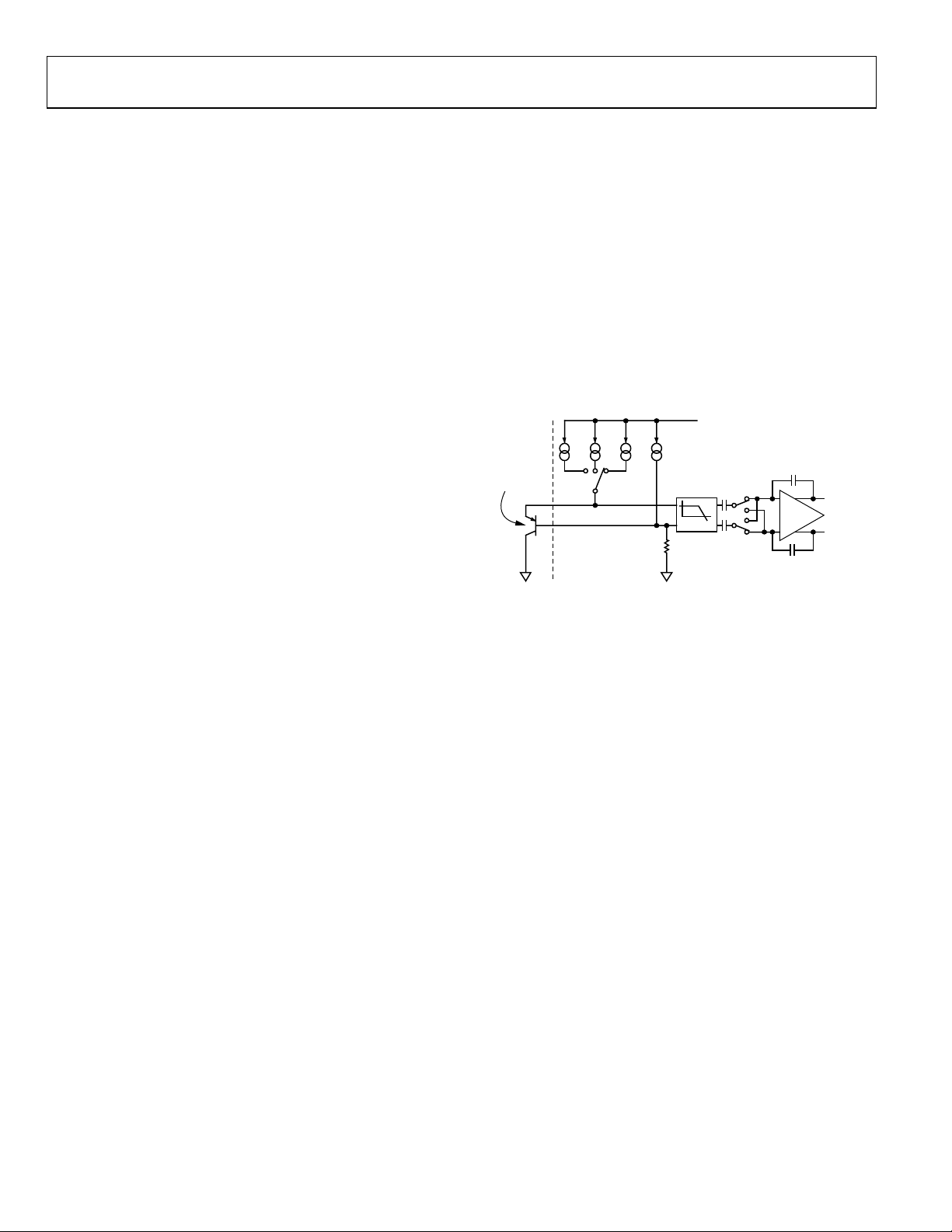
Figure 23 shows the input signal conditioning used to measure
the output of a remote temperature sensor. This figure shows
the external sensor as a substrate transistor, provided for
temperature monitoring on some microprocessors. It could also
be a discrete transistor such as a 2N3904/2N3906.
V
N2 × IIN1× II
REMOTE
SENSING
TRANSISTOR
D+
D–
Figure 23. Signal Conditioning for Remote Diode Temperature Sensors
BIAS
fC = 65kHz
LPF
DD
V
OUT+
TO ADC
V
OUT–
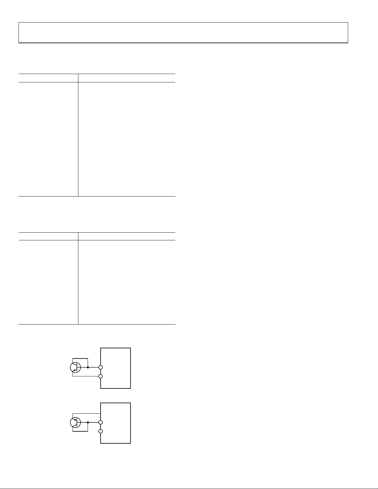
If a discrete transistor is used, the collector is not grounded and
should be linked to the base. If a PNP transistor is used, the base
is connected to the D– input and the emitter to the D+ input. If
an NPN transistor is used, the emitter is connected to the D–
input and the base to the D+ input. Figure 25 and Figure 26
show how to connect the ADT7468 to an NPN or PNP
transistor for temperature measurement. To prevent ground
noise from interfering with the measurement, the more negative
terminal of the sensor is not referenced to ground, but is biased
above ground by an internal diode at the D– input.
To m e as u re ∆ V
, the operating current through the sensor is
BE
switched among three related currents. Shown in Figure 23,
N1 × I and N2 × I are different multiples of the current I. The
currents through the temperature diode are switched between
I and N1 × I, giving ∆V
giving ∆V
the two ∆V
. The temperature can then be calculated using
BE2
measurements. This method can also cancel the
BE
, and then between I and N2 × I,
BE1
effect of any series resistance on the temperature measurement.
04499-0-012
The forward voltage of a diode or diode-connected transistor
operated at a constant current exhibits a negative temperature
coefficient of about –2 mV/°C. Unfortunately, the absolute value
varies from device to device and individual calibration is
of V
BE
required to null this out, so the technique is unsuitable for mass
production. The technique used in the ADT7468 is to measure
the change in V
when the device is operated at three different
BE
The resulting ∆V
low-pass filter to remove noise and then to a chopper-stabilized
amplifier. This amplifies and rectifies the waveform to produce
a dc voltage proportional to ∆V
voltage, and a temperature measurement is produced. To reduce
the effects of noise, digital filtering is performed by averaging
the results of 16 measurement cycles.
waveforms are passed through a 65 kHz
BE
. The ADC digitizes this
BE
currents.
Rev. 0 | Page 18 of 80

ADT7468
T
The results of remote temperature measurements are stored in
10-bit, twos complement format, as illustrated in Table 6. The
extra resolution for the temperature measurements is held in
the Extended Resolution Register 2 (Reg. 0x77). This gives
temperature readings with a resolution of 0.25°C.
Noise Filtering
For temperature sensors operating in noisy environments,
previous practice was to place a capacitor across the D+ and D−
pins to help combat the effects of noise. However, large capacitances affect the accuracy of the temperature measurement,
leading to a recommended maximum capacitor value of 1000 pF.
This capacitor reduces the noise, but does not eliminate it, making
use the sensor difficult in a very noisy environment.
The ADT7468 has a major advantage over other devices for
eliminating the effects of noise on the external sensor. Using the
series resistance cancellation feature, a filter can be constructed
between the external temperature sensor and the part. The effect
of any filter resistance seen in series with the remote sensor is
automatically canceled from the temperature result.
The construction of a filter allows the ADT7468 and the remote
temperature sensor to operate in noisy environments. Figure 24
shows a low-pass R-C-R filter, with the following values :
R = 100 Ω, C = 1 nF.
This filtering reduces both common-mode noise and
differential noise.
100Ω
REMOTE
EMPERATURE
SENSOR
Figure 24. Filter Between Remote Sensor and ADT7468
100Ω
1nF
D+
D–
04499-0-093
SERIES RESISTANCE CANCELLATION
Parasitic resistance to the ADT7468 D+ and D− inputs (seen in
series with the remote diode) is caused by a variety of factors,
including PCB track resistance and track length. This series
resistance appears as a temperature offset in the remote sensor’s
temperature measurement. This error typically causes a 0.5°C
offset per Ω of parasitic resistance in series with the remote
diode.
The ADT7468 automatically cancels out the effect of this series
resistance on the temperature reading, giving a more accurate
result, without the need for user characterization of this
resistance. The ADT7468 is designed to automatically cancel,
typically, up to 3 kΩ of resistance. By using an advanced
temperature measurement method, this is transparent to the
user. This feature allows resistances to be added to the sensor
path to produce a filter, allowing the part to be used in noisy
environments. See the Noise Filtering section for details.
FACTORS AFFECTING DIODE ACCURACY
Remote Sensing Diode
The ADT7468 is designed to work with either substrate
transistors built into processors or with discrete transistors.
Substrate transistors are generally PNP types with the collector
connected to the substrate. Discrete types can be either PNP or
NPN transistors connected as a diode (base-shorted to the
collector). If an NPN transistor is used, the collector and base
are connected to D+ and the emitter to D−. If a PNP transistor
is used, the collector and base are connected to D− and the
emitter is connected to D+.
To reduce the error due to variations in both substrate and
discrete transistors, a number of factors should be taken into
consideration:
•
The ideality factor, n
deviation of the thermal diode from ideal behavior. The
ADT7468 is trimmed for an n
following equation to calculate the error introduced at a
temperature T (°C), when using a transistor whose n
not equal 1.008. See the processor data sheet for the n
values.
∆T = (n
− 1.008) × (273.15 K + T)
f
To factor this in, the user can write the ∆T value to the
offset register. The ADT7468 then automatically adds it to
or subtracts it from the temperature measurement.
Some CPU manufacturers specify the high and low current
•
levels of the substrate transistors. The high current level of
the ADT7468, I
is 6 µA. If the ADT7468 current levels do not match the
current levels specified by the CPU manufacturer, it might
be necessary to remove an offset. The CPUs data sheet
advises whether this offset needs to be removed and how to
calculate it. This offset can be programmed to the offset
register. It is important to note that, if more than one offset
must be considered, the algebraic sum of these offsets must
be programmed to the offset register.
If a discrete transistor is used with the ADT7468, the best
accuracy is obtained by choosing devices according to the
following criteria:
•
Base-emitter voltage greater than 0.25 V at 6 µA, at the
highest operating temperature.
•
Base-emitter voltage less than 0.95 V at 100 µA, at the
lowest operating temperature.
•
Base resistance less than 100 Ω.
•
Small variation in h
control of V
BE
, of the transistor is a measure of the
f
value of 1.008. Use the
f
, is 96 µA and the low level current, I
HIGH
(say 50 to 150) that indicates tight
FE
characteristics.
does
f
f
LOW
,
Rev. 0 | Page 19 of 80
ADT7468
2
2
Transistors, such as 2N3904, 2N3906, or equivalents in SOT-23
packages, are suitable devices to use.
Table 6. Temperature Data Format
Temperature Digital Output (10-Bit)1
–128°C
–125°C
–100°C
–75°C
–50°C
–25°C
–10°C
0°C
10.25°C
25.5°C
50.75°C
75°C
100°C
125°C
127°C
1
Bold numbers denote 2 LSB of measurement in Extended Resolution
Register 2 (Reg. 0x77) with 0.25°C resolution.
Table 7. Extended Range, Temperature Data Format
Temperature Digital Output (10-Bit)1
–64°C
–1°C
0°C
1°C
10°C
25°C
50°C
75°C
100°C
125°C
191°C
1
Bold numbers denote 2 LSB of measurement in Extended Resolution
Register 2 (Reg. 0x77) with 0.25°C resolution.
1000 0000 00
1000 0011 00
1001 1100 00
1011 0101 00
1100 1110 00
1110 0111 00
1111 0110 00
0000 0000 00
0000 1010 01
0001 1001 10
0011 0010 11
0100 1011 00
0110 0100 00
0111 1101 00
0111 1111 00
0000 0000 00
0011 1111 00
0100 0000 00
0100 0001 00
0100 1010 00
0101 1001 00
0111 0010 00
1000 1001 00
1010 0100 00
1011 1101 00
1111 1111 00
ADT7468
Nulling Out Temperature Errors
As CPUs run faster, it is getting more difficult to avoid high
frequency clocks when routing the D+/D– traces around a
system board. Even when recommended layout guidelines are
followed, some temperature errors may still be attributable to
noise coupled onto the D+/D– lines. Constant high frequency
noise usually attenuates or increases temperature measurements
by a linear, constant value.
The ADT7468 has temperature offset registers at Addresses
0x70, 0x72 for the Remote 1 and Remote 2 temperature
channels. By doing a one-time calibration of the system, the
user can determine the offset caused by system board noise and
null it out using the offset registers. The offset registers
automatically add an Offset 64/twos complement 8-bit reading
to every temperature measurement. The LSBs add 0.5°C offset
to the temperature reading so the 8-bit register effectively allows
temperature offsets of up to ±64°C with a resolution of 0.5°C.
This ensures that the readings in the temperature measurement
registers are as accurate as possible.
Temperature Offset Registers
Reg. 0x70, Remote 1 Temperature Offset = 0x00 (0°C default)
Reg. 0x71,
Reg. 0x72,
Local Temperature Offset = 0x00 (0°C default)
Remote 2 Temperature Offset = 0x00 (0°C default)
ADT7463/ADT7468 Backwards Compatible Mode
By setting Bit 1 of Configuration Register 5 (0x7C), all temperature measurements are stored in the Zone Temp value registers
(0x25, 0x26, and 0x27) in twos complement in the range −64°C
to +127°C (the ADT7468 still makes calculations based on the
Offset 64 extended range and clamps the results, if necessary.)
The temperature limits must be reprogrammed in twos
complement. If a twos complement temperature below −63°C is
entered, the temperature is clamped to −63°C. In this mode, the
diode fault condition remains −128°C = 1000 0000, while in the
extended temperature range (−64°C to +191°C), the fault
condition is represented by −64°C = 0000 0000.
Temperature Measurement Registers
Reg. 0x25, Remote 1 Temperature
N3904
NPN
Figure 25. Measuring Temperature Using an NPN Transistor
D+
D–
ADT7468
04499-0-013
Reg. 0x26,
Reg. 0x27,
Reg. 0x77,
<7:6> TDM2, Remote 2 temperature LSBs.
Local Temperature
Remote 2 Temperature
Extended Resolution 2 = 0x00 default
<5:4> LTMP, local temperature LSBs.
N3906
PNP
Figure 26. Measuring Temperature Using a PNP Transistor
D+
D–
04499-0-014
Rev. 0 | Page 20 of 80
<3:2> TDM1, Remote 1 temperature LSBs.
ADT7468
Temperature Measurement Limit Registers
Associated with each temperature measurement channel are
high and low limit registers. Exceeding the programmed high or
low limit causes the appropriate status bit to be set. Exceeding
either limit can also generate
Reg. 0x4E,
Reg. 0x4F,
Reg. 0x50,
Remote 1 Temperature Low Limit = 0x01 default
Remote 1 Temperature High Limit = 0x7F default
Local Temperature Low Limit = 0x01 default
SMBALERT
interrupts.
Reg. 0x51, Local Temperature High Limit = 0x7F default
Reg. 0x52,
Reg. 0x53,
Remote 2 Temperature Low Limit = 0x01 default
Remote 2 Temperature High Limit = 0x7F default
Reading Temperature from the ADT7468
It is important to note that temperature can be read from the
ADT7468 as an 8-bit value (with 1°C resolution) or as a 10-bit
value (with 0.25°C resolution). If only 1°C resolution is
required, the temperature readings can be read back at any
time and in no particular order.
Table 9. Conversion Time with Averaging Enabled
Channel Measurement Time
Voltage Channels 11 ms
Remote Temperature 39 ms
Local Temperature 12 ms
Single-Channel ADC Conversions
Setting Bit 6 of Configuration Register 2 (Reg. 0x73) places the
ADT7468 into single-channel ADC conversion mode. In this
mode, the ADT7468 can be made to read a single temperature
channel only. The appropriate ADC channel is selected by
writing to Bits <7:5> of the TACH1 minimum high byte register
(0x55).
Table 10. Channel Selection
Bits <7:5> Reg. 0x55 Channel Selected
101 Remote 1 temperature
110 Local temperature
111 Remote 2 temperature
Configuration Register 2 (Reg. 0x73)
<4> = 1,
averaging off.
If the 10-bit measurement is required, this involves a 2-register
read for each measurement. The extended resolution register
(Reg. 0x77) should be read first. This causes all temperature
reading registers to be frozen until all temperature reading
registers have been read from. This prevents an MSB reading
from being updated while its two LSBs are being read and
vice versa.
ADDITIONAL ADC FUNCTIONS FOR TEMPERATURE MEASUREMENT
A number of other functions are available on the ADT7468 to
offer the system designer increased flexibility.
Turn-Off Averaging
For each temperature measurement read from a value register,
16 readings have actually been made internally and the results
averaged before being placed into the value register. Sometimes
it is necessary to take a very fast measurement. Setting Bit 4 of
Configuration Register 2 (Reg. 0x73) turns averaging off.
<6> = 1, single-channel convert mode.
TACH1 Minimum High Byte (Reg. 0x55)
<7:5>
selects ADC channel for single-channel convert mode.
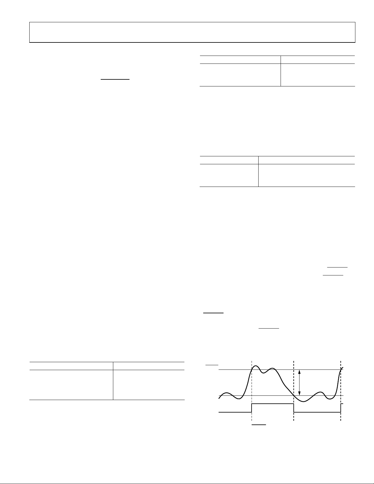
Overtemperature Events
Overtemperature events on any of the temperature channels can
be detected and dealt with automatically in automatic fan speed
control mode. Register 0x6A to Register 0x6C are the
temperature limits. When a temperature exceeds its
temperature limit, all PWM outputs run at the maximum PWM
duty cycle (Reg. 0x38, Reg. 0x39, and Reg. 0x3A). This
effectively runs the fans at the fastest allowed speed. The fans
stay running at this speed until the temperature drops below
THERM
boost bit in Configuration Register 3, Bit 2, Reg. 0x78.) The
hysteresis value for that
programmed into Reg. 0x6D and Reg. 0x6E (hysteresis
registers). The default hysteresis value is 4°C.
Table 8. Conversion Time with Averaging Disabled
Channel Measurement Time
Voltage Channels 0.7 ms
Remote Temperature 1 7 ms
Remote Temperature 2 7 ms
Local Temperature 1.3 ms
THERM LIMIT
TEMPERATURE
FANS
THERM
THERM
minus hysteresis. (This can be disabled by setting the
Figure 27.
THERM
THERM
temperature limit is the value
HYSTERESIS (°C)
100%
Temperature Limit Operation
04499-0-015
Rev. 0 | Page 21 of 80

ADT7468
LIMITS, STATUS REGISTERS, AND INTERRUPTS
LIMIT VALUES
Associated with each measurement channel on the ADT7468
are high and low limits. These can form the basis of system
status monitoring; a status bit can be set for any out-of-limit
condition and detected by polling the device. Alternatively,
SMBALERT
microcontroller of out-of-limit conditions.
8-Bit Limits
The following is a list of 8-bit limits on the ADT7468.
Volt ag e Li mi t Re g is ter s
Reg. 0x44, 2.5 V Low Limit = 0x00 default
Reg. 0x45,
Reg. 0x46,
Reg. 0x47,
Reg. 0x48,
Reg. 0x49,
Reg. 0x4A,
Reg. 0x4B,
Reg. 0x4C,
Reg. 0x4D,
Reg. 0x46, V
Reg. 0x47,
Reg. 0x48,
interrupts can be generated to flag a processor or
2.5 V High Limit = 0xFF default
V
Low Limit = 0x00 default
CCP
V
High Limit = 0xFF default
CCP
VCC Low Limit = 0x00 default
VCC High Limit = 0xFF default
5 V Low Limit = 0x00 default
5 V High Limit = 0xFF default
12 V Low Limit = 0x00 default
12 V High Limit = 0xFF default
Low Limit = 0x00 default
CCP
V
High Limit = 0xFF default
CCP
VCC Low Limit = 0x00 default
THERM
Reg. 0x7A,
Limit Register
THERM
Limit = 0x00 default
16-Bit Limits
The fan TACH measurements are 16-bit results. The fan TACH
limits are also 16 bits, consisting of a high byte and low byte.
Because fans running under speed or stalled are normally the
only conditions of interest, only high limits exist for fan TACHs.
Because the fan TACH period is actually being measured,
exceeding the limit indicates a slow or stalled fan.
Fan Limit Registers
Reg. 0x54, TA C H1 M i ni m u m L ow B y te = 0x00 default
Reg. 0x55,
Reg. 0x56,
Reg. 0x57,
Reg. 0x58,
Reg. 0x59,
Reg. 0x5A,
Reg. 0x5B,
TAC H1 M ini m u m Hi g h B y te = 0x00 default
TAC H2 M ini m u m L ow B y te = 0x00 default
TAC H2 M ini m u m Hi g h B y te = 0x00 default
TAC H3 M ini m u m L ow B y te = 0x00 default
TAC H3 M ini m u m Hi g h B y te = 0x00 default
TAC H4 M ini m u m L ow B y te = 0x00 default
TAC H4 M ini m u m Hi g h B y te = 0x00 default
Out-of-Limit Comparisons
Once all limits have been programmed, the ADT7468 can be
enabled for monitoring. The ADT7468 measures all voltage and
temperature measurements in round-robin format and sets the
appropriate status bit for out-of-limit conditions. TACH
measurements are not part of this round-robin cycle. Comparisons are done differently depending on whether the measured
value is being compared to a high or low limit.
Reg. 0x49,
VCC High Limit = 0xFF default
Temperature Limit Registers
Reg. 0x4E, Remote 1 Temperature Low Limit = 0x01 default
Reg. 0x4F,
Reg. 0x6A,
Reg. 0x50,
Reg. 0x51,
Reg. 0x6B, Local
Reg. 0x52,
Reg. 0x53,
Reg. 0x6C,
Remote 1 Temperature High Limit = 0x7F default
Remote 1
THERM
Limit = 0x64 default
Local Temperature Low Limit = 0x01 default
Local Temperature High Limit = 0x7F default
THERM
Limit = 0x64 default
Remote 2 Temperature Low Limit = 0x01 default
Remote 2 Temperature High Limit = 0x7F default
Remote 2
THERM
Limit = 0x64 default
High Limit: > Comparison Performed
Low Limit: ≤ Comparison Performed
Voltage and temperature channels use a window comparator for
error detecting and, therefore, have high and low limits. Fan
speed measurements use only a low limit. This fan limit is
needed only in manual fan control mode.
Analog Monitoring Cycle Time
The analog monitoring cycle begins when a 1 is written to the
start bit (Bit 0) of Configuration Register 1 (Reg. 0x40). By
default, the ADT7463 powers up with this bit set. The ADC
measures each analog input in turn and, as each measurement is
completed, the result is automatically stored in the appropriate
value register. This round-robin monitoring cycle continues
unless disabled by writing a 0 to Bit 0 of Configuration
Register 1.
Rev. 0 | Page 22 of 80

ADT7468
As the ADC is normally left to free-run in this manner, the time
taken to monitor all the analog inputs is normally not of
interest, because the most recently measured value of any input
can be read out at any time.
For applications where the monitoring cycle time is important,
it can easily be calculated.
The total number of channels measured is
•
Four dedicated supply voltage inputs
Supply voltage (V
•
•
Local temperature
Two remote temperatures
•
CC
pin)
As mentioned previously, the ADC performs round-robin
conversions and takes 11 ms for each voltage measurement,
12 ms for a local temperature reading, and 39 ms for each
remote temperature reading. The total monitoring cycle time
for averaged voltage and temperature monitoring is, therefore,
nominally
Status Register 1 (Reg. 0x41)
Bit 7 (OOL) = 1
, denotes a bit in Status Register 2 is set and
Status Register 2 should be read.
Bit 6 (R2T) = 1, Remote 2 temperature high or low limit has
been exceeded.
Bit 5 (LT) = 1, local temperature high or low limit has been
exceeded.
Bit 4 (R1T) = 1, Remote 1 temperature high or low limit has
been exceeded.
Bit 3 (5 V) = 1, 5 V high or low limit has been exceeded.
Bit 2 (V
Bit 1 (V
) = 1, V
CC
) = 1, V
CCP
high or low limit has been exceeded.
CC
high or low limit has been exceeded.
CCP
Bit 0 (2.5 V) = 1, 2.5 V high or low limit has been exceeded.
Status Register 2 (Reg. 0x42)
Bit 7 (D2) = 1
, indicates an open or short on D2+/D2– inputs.
Bit 6 (D1) = 1, indicates an open or short on D1+/D1– inputs.
(5 × 11) + 12 + (2 × 39) = 145 ms
Fan TACH measurements are made in parallel and are not
synchronized with the analog measurements in any way.
STATUS REGISTERS
The results of limit comparisons are stored in Status Registers 1
and 2. The status register bit for each channel reflects the status
of the last measurement and limit comparison on that channel.
If a measurement is within limits, the corresponding status
register bit is cleared to 0. If the measurement is out-of-limits,
the corresponding status register bit is set to 1.
The state of the various measurement channels can be polled by
reading the status registers over the serial bus. In Bit 7 (OOL) of
Status Register 1 (Reg. 0x41), 1 means that an out-of-limit event
has been flagged in Status Register 2. This means that the user
also needs to read Status Register 2. Alternatively, Pin 10 or Pin
14 can be configured as an
interrupt automatically notifies the system supervisor of an outof-limit condition. Reading the status registers clears the
appropriate status bit as long as the error condition that caused
the interrupt has cleared. Status register bits are “sticky.”
Whenever a status bit is set, indicating an out-of-limit
condition, it remains set even if the event that caused it has
gone away (until read). The only way to clear the status bit is to
read the status register after the event has gone away. Interrupt
status mask registers (Reg. 0x74, and Reg. 0x75) allow individual
interrupt sources to be masked from causing an
However, if one of these masked interrupt sources goes out-oflimit, its associated status bit is set in the interrupt status
registers.
SMBALERT
output. This hard
SMBALERT
.
Bit 5 (F4P) = 1, indicates Fan 4 has dropped below minimum
speed. Alternatively, indicates that the
exceeded, if the
THERM
function is used.
THERM
limit has been
Bit 4 (FAN3) = 1, indicates Fan 3 has dropped below minimum
speed.
Bit 3 (FAN2) = 1, indicates Fan 2 has dropped below minimum
speed.
Bit 2 (FAN1) = 1, indicates Fan 1 has dropped below minimum
speed.
Bit 1 (OVT) = 1, indicates a
THERM
overtemperature limit has
been exceeded.
Bit 0 (12V/VC) = 1, indicates a 12 V high or low limit has been
exceeded. If the VID code change function is used, this bit
indicates a change in VID code on the VID0 to VID5 inputs.
SMBALERT
The ADT7468 can be polled for status, or an
Interrupt Behavior
SMBALERT
interrupt can be generated for out-of-limit conditions. It is
important to note how the
SMBALERT
output and status bits
behave when writing interrupt handler software.
Rev. 0 | Page 23 of 80
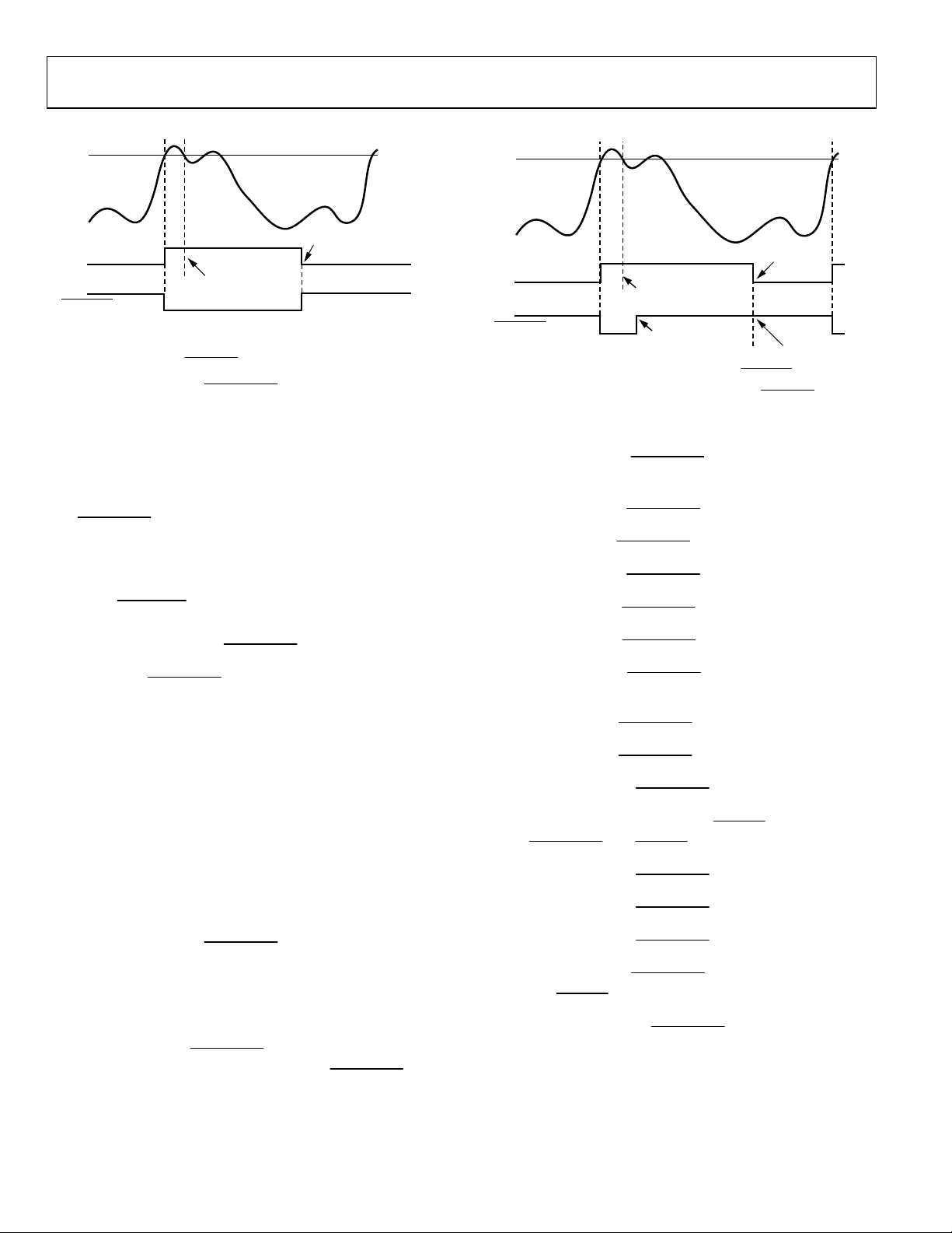
ADT7468
T
HIGH LIMIT
TEMPERATURE
CLEARED ON READ
“STICKY”
STATUS BI
TEMP BACK IN LIMIT
SMBALERT
Figure 28.
(STATUS BIT STAYS SET)
SMBALERT
Figure 28 shows how the
and Status Bit Behavior
SMBALERT
(TEMP BELOW LIMIT)
output and “sticky” status
bits behave. Once a limit is exceeded, the corresponding status
bit is set to 1. The status bit remains set until the error condition
subsides and the status register is read. The status bits are
referred to as “sticky,” because they remain set until read by
software. This ensures that an out-of-limit event cannot be
missed, if software is polling the device periodically. Note that
SMBALERT
the
output remains low for the entire duration that
a reading is out-of-limit and until the status register has been
read. This has implications on how software handles the
interrupt.
Handling
SMBALERT
Interrupts
To prevent the system from being tied up servicing interrupts, it
is recommend to handle the
SMBALERT
interrupt as follows:
04499-0-022
HIGH LIMIT
TEMPERATURE
“STICKY”
STATUS BIT
SMBALERT
Figure 29. How Masking the Interrupt Source Affects
TEMP BACK IN LIMIT
(STATUS BIT STAYS SET)
INTERRUPT
MASK BIT SET
Interrupt Mask Register 1 (Reg. 0x74)
Bit 7 (OOL) = 1
, masks
SMBALERT
for any alert condition
flagged in Status Register 2.
Bit 6 (R2T) = 1, masks
Bit 5 (LT) = 1, masks
Bit 4 (R1T) = 1, masks
Bit 3 (5 V) = 1, masks
Bit 2 (VCC) = 1, masks
SMBALERT
SMBALERT
SMBALERT
SMBALERT
SMBALERT
for Remote 2 temperature.
for local temperature.
for Remote 1 temperature.
for 5 V channel.
for VCC channel.
CLEARED ON READ
(TEMP BELOW LIMIT)
INTERRUPT MASK BIT
CLEARED
(SMBALERT REARMED)
SMBALERT
Output
04499-0-023
Detect the
1.
2.
Enter the interrupt handler.
3.
Read the status registers to identify the interrupt source.
4.
Mask the interrupt source by setting the appropriate mask
SMBALERT
assertion.
bit in the interrupt mask registers (Reg. 0x74 and
Reg. 0x75).
5.
Take the appropriate action for a given interrupt source.
6.
Exit the interrupt handler.
7.
Periodically poll the status registers. If the interrupt status
bit has cleared, reset the corresponding interrupt mask bit
to 0. This causes the
SMBALERT
output and status bits to
behave as shown in Figure 29.
Masking Interrupt Sources
Interrupt Mask Registers 1 and 2 are located at Addresses 0x74
and 0x75. These allow individual interrupt sources to be
masked out to prevent
masking an interrupt source prevents only the
SMBALERT
interrupts. Note that
SMBALERT
output from being asserted; the appropriate status bit is set
normally.
Bit 0 (V
) = 1, masks
CCP
SMBALERT
for V
channel.
CCP
Interrupt Mask Register 2 (Reg. 0x75)
Bit 7 (D2) = 1
Bit 6 (D1) = 1, masks
Bit 5 (FAN4) = 1, masks
If the TACH4 pin is being used as the
SMBALERT
masks
Bit 4 (FAN3) = 1, masks
Bit 3 (FAN2) = 1, masks
Bit 2 (FAN1) = 1, masks
Bit 1 (OVT) = 1, masks
(exceeding
THERM
Bit 0 (12V/VC) = 1, masks
SMBALERT
, masks
SMBALERT
SMBALERT
THERM
for a
SMBALERT
SMBALERT
SMBALERT
SMBALERT
temperature limits).
SMBALERT
for Diode 2 errors.
for Diode 1 errors.
for Fan 4 failure.
THERM
input, this bit
event.
for Fan 3.
for Fan 2.
for Fan 1.
for overtemperature
for 12 V channel or for
a VID code change, depending on the function used.
Rev. 0 | Page 24 of 80
 Loading...