

dB
COOL™ Remote Thermal
FEATURES
Controls and monitors up to 4 fan speeds
1 on-chip and 2 remote temperature sensors
Dynamic T
intelligently
Automatic fan speed control mode controls system cooling
based on measured temperature
Enhanced acoustic mode dramatically reduces user
perception of changing fan speeds
Thermal protection feature via
Monitors performance impact of Intel®
Processor thermal control circuit via
2-wire and 3-wire fan speed measurement
Limit comparison of all monitored values
Meets SMBus 2.0 electrical specifications (fully
SMBus 1.1-compliant)
APPLICATIONS
Low acoustic noise PCs
Networking and telecommunications equipment
control mode optimizes system acoustics
MIN
output
THERM
Pentium® 4
input
THERM
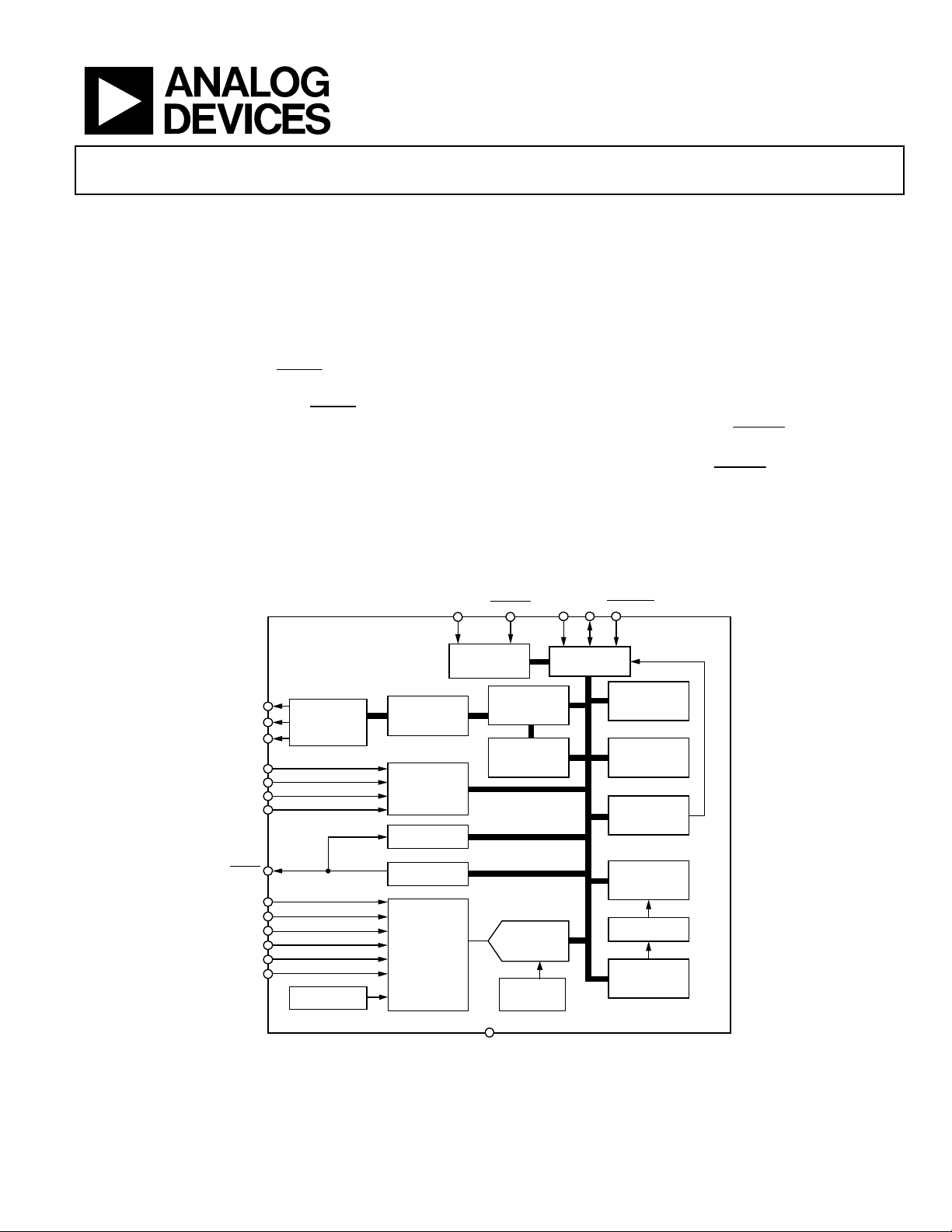
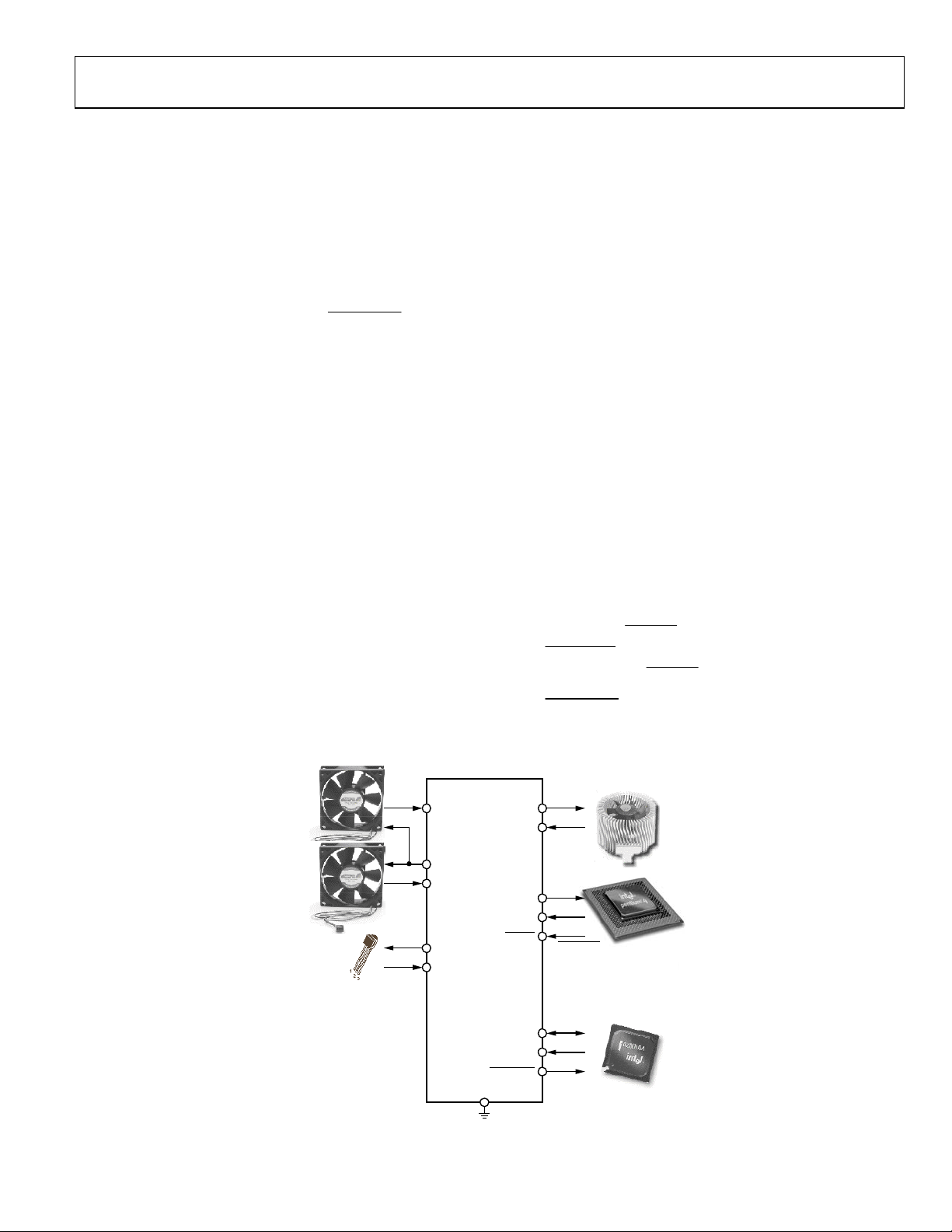
FUNCTIONAL BLOCK DIAGRAM
ADDR
SELECT
Controller and Fan Controller
ADT7460
GENERAL DESCRIPTION
The ADT74601 dBCOOL controller is a thermal monitor and
multiple PWM fan controller for noise-sensitive applications
requiring active system cooling. It can monitor the temperature
of up to two remote sensor diodes plus its own internal temperature. It can measure and control the speed of up to four fans
so that they operate at the lowest possible speed for minimum
acoustic noise. The automatic fan speed control loop optimizes
fan speed for a given temperature. A unique dynamic T
control mode enables the system thermals/acoustics to be
intelligently managed. The effectiveness of the system’s thermal
solution can be monitored using the
THERM
ADT7460 also provides critical thermal protection to the
system by using the bidirectional
THERM
to prevent system or component overheating.
ADDR_EN
SCL
SDA
SMBALERT
input. The
pin as an output
MIN
PWM1
PWM2
PWM3
TACH1
TACH2
TACH3
TACH4
THERM
V
D1+
D1–
D2+
D2–
+2.5V
CC
IN
PWM REGISTERS
AND
CONTROLLERS
VCCTO ADT7460
BAND GAP
TEMP SENSOR
ACOUSTIC
ENHANCEMENT
CONTROL
FAN SPEED
COUNTER
PERFORMANCE
MONITORING
THERMAL
PROTECTION
INPUT
SIGNAL
CONDITIONING
AND
ANALOG
MULTIPLEXER
SMBUS
ADDRESS
SELECTION
GND
AUTOMATIC
FAN SPEED
CONTROL
DYNAMIC
CONTROL
ADT7460
10-BIT
BAND GAP
REFERENCE
T
MIN
ADC
SERIAL BUS
INTERFACE
Figure 1.
1
Protected by U.S. Patent Nos. 6,188,189; 6,169,442; 6,097,239; 5,982,221; and 5,867,012. Other patents pending.
Rev. C
Information furnished by Analog Devices is believed to be accurate and reliable.
However, no responsibility is assumed by Analog Devices for its use, nor for any
infringements of patents or other rights of third parties that may result from its use.
Specifications subject to change without notice. No license is granted by implication
or otherwise under any patent or patent rights of Analog Devices. Trademarks and
registered trademarks are the property of their respective owners.
One Technology Way, P.O. Box 9106, Norwood, MA 02062-9106, U.S.A.
Tel: 781.329.4700
Fax: 781.461.3113 © 2005 Analog Devices, Inc. All rights reserved.
ADDRESS
POINTER
REGISTER
PWM
CONFIGURATION
REGISTERS
INTERRUPT
MASKING
INTERRUPT
STATUS
REGISTERS
LIMIT
COMPARATORS
VALUE AND
LIMIT
REGISTERS
03228-001
www.analog.com

ADT7460
TABLE OF CONTENTS
Specifications..................................................................................... 3
Additional ADC Functions for Voltage Measurements........ 17
Absolute Maximum Ratings............................................................ 5
Thermal Characteristics .............................................................. 5
ESD Caution.................................................................................. 5
Pin Configuration and Function Descriptions............................. 6
Typical Performance Characteristics ............................................. 7
Product Description ......................................................................... 9
Measurement Inputs .................................................................... 9
Sequential Measurement ............................................................. 9
Recommended Implementation................................................. 9
ADT7460 Address Selection..................................................... 10
Internal Registers of the ADT7460 .......................................... 10
Theory of Operation ...................................................................... 11
Serial Bus Interface..................................................................... 11
Voltage Measurement Input...................................................... 15
Temperature Measurement System.......................................... 17
Additional ADC Functions for Temperature Measurement 19
Limits, Status Registers, and Interrupts................................... 20
Status Registers ........................................................................... 21
Handling
THERM
SMBALERT
Interrupts............................................. 22
Timer ........................................................................... 24
Fan Drive Using PWM Control ............................................... 27
Operating from 3.3 V Standby ................................................. 33
XNOR Tree Test Mode .............................................................. 33
Power-On Default ...................................................................... 33
ADT7460 Register Summary........................................................ 34
Outline Dimensions ....................................................................... 51
Ordering Guide .......................................................................... 51
REVISION HISTORY
3/05—Rev. B to Rev. C
Updated Format .................................................................. Universa
Changes to Absolute Maximum Ratings Table..............................5
Changes to ADT7460 Register Map Summary Section .............34
Updated Ordering Guide................................................................51
9/03—Rev. A to Rev. B
Changed XOR Tree Test Mode to XNOR ............................Universal
Changes to SPECIFICATIONS.............................................................2
Changes to TPC 7.................................................................................... 7
6/03—Rev. 0 to Rev. A
l
Updated ORDERING ............................................................................4
Updated the SERIAL BUS INTERFACE section................................9
Added the To Assign
Added the
Renamed the Therm Input section to
Renumbered the figures after Figure 25.............................................22
Updated Step 1 in the Configuring the Desired
section........................................................................................................2
Updated the Fan Speed Control section ............................................28
Added the POWER-ON DEFAULT section .....................................29
Updated Table IV ..................................................................................30
Updated Table XVIII ............................................................................38
Updated Table XX .................................................................................40
Updated Table XXXV ...........................................................................46
Updated OUTLINE DIMENSIONS ...................................................49
THERM
THERM
as an Input section.............................................21
Functionality to a Pin 9 section ....21
THERM
Timer ....................21
THERM
Behavior
Rev. C | Page 2 of 52

ADT7460
SPECIFICATIONS
TA = T
Table 1.
Parameter
POWER SUPPLY
20 µA Standby mode
TEMPERATURE-TO-DIGITAL CONVERTER
11 µA Low level
ANALOG-TO-DIGITAL CONVERTER
(INCLUDING MUX AND ATTENUATORS)
FAN RPM-TO-DIGITAL CONVERTER
OPEN-DRAIN DIGITAL OUTPUTS, PWM1–PWM3, XTO
OPEN-DRAIN SERIAL DATA BUS OUTPUT (SDA)
Output Low Voltage, V
High Level Output Current, I
SMBUS DIGITAL INPUTS (SCL, SDA)
MIN
to T
1, , 2 3
, VCC = V
MAX
MIN
to V
, unless otherwise noted.
MAX
Min Typ
4
Max Unit Test Conditions/Comments
Supply Voltage 3.0 5.0 5.5 V
Supply Current, I
CC
3 mA Interface inactive, ADC active
Local Sensor Accuracy ±1.5 °C 0°C ≤ TA ≤ 70°C
±3 °C −40°C ≤ TA ≤ +120°C
Resolution 0.25 °C
Remote Diode Sensor Accuracy ±1.5 °C 0°C ≤ TA ≤ 70°C; 0°C ≤ TD ≤ 120°C
±2.5 °C 0°C ≤ TA ≤ 105°C; 0°C ≤ TD ≤ 120°C
±3 °C 0°C ≤ TA ≤ 120°C; 0°C ≤ TD ≤ 120°C
Resolution 0.25 °C
Remote Sensor Source Current 180 µA High level
Total Unadjusted Error, TUE ±1.5 %
Differential Nonlinearity, DNL ±1 LSB 8 bits
Power Supply Sensitivity ±0.1 %/V
Conversion Time (Voltage Input) 11.38 13 ms Averaging enabled
Conversion Time (Local Temperature) 12.09 13.50 ms Averaging enabled
Conversion Time (Remote Temperature) 25.59 28 ms Averaging enabled
Total Monitoring Cycle Time 120.17 134.50 ms Averaging enabled (incl. delay5)
13.51 15 ms Averaging disabled
Input Resistance 80 140 200 kΩ
Accuracy ±7 % 0°C ≤ TA ≤ 70°C
±11 % 0°C ≤ TA ≤ 105°C
±13 % −40°C ≤ TA ≤ +120°C
Full-Scale Count 65,535
Nominal Input RPM 109 RPM Fan count = 0xBFFF
329 RPM Fan count = 0x3FFF
5000 RPM Fan count = 0x0438
10000 RPM Fan count = 0x021C
Internal Clock Frequency 82.8 90.0 97.2 kHz
Current Sink, I
Output Low Voltage, V
OL
OL
High Level Output Current, I
OL
OH
Input High Voltage, V
Input Low Voltage, V
IH
IL
OH
8.0 mA
0.4 V I
0.1 1 µA V
0.4 V I
0.1 1 µA V
= −8.0 mA, VCC = 3.3 V
OUT
= V
OUT
= −4.0 mA, VCC = 3.3 V
OUT
= V
OUT
2.0 V
0.4 V
CC
CC
Hysteresis 500 mV
Rev. C | Page 3 of 52

ADT7460
A
Parameter
1, 2, 3
Min Typ
4
Max Unit Test Conditions/Comments
DIGITAL INPUT LOGIC LEVELS (TACH INPUTS)
Input High Voltage, V
IH
2.0 V
5.5 V Maximum input voltage
Input Low Voltage, V
IL
+0.8 V
−0.3 V Minimum input voltage
Hysteresis 0.5 V p-p
DIGITAL INPUT LOGIC LEVELS (THERM)
Input High Voltage, V
Input Low Voltage, V
IH
IL
1.7 V
0.8 V
DIGITAL INPUT CURRENT
Input High Current, I
Input Low Current, I
Input Capacitance, C
SERIAL BUS TIMING
Clock Frequency, f
Glitch Immunity, t
Bus Free Time, t
Start Setup Time, t
Start Hold Time, t
SCL Low Time, t
SCL High Time, t
SCL, SDA Rise Time, t
SCL, SDA Fall Time, t
Data Setup Time, t
Detect Clock Low Timeout, t
1
All voltages are measured with respect to GND, unless otherwise specified.
2
Logic inputs accept input high voltages up to V
3
Timing specifications are tested at logic levels of VIL = 0.8 V for a falling edge and at VIH = 2.0 V for a rising edge.
4
Typicals are at TA = 25°C and represent the most likely parametric norm.
5
The delay is the time between the round robin finishing one set of measurements and starting the next.
6
Guaranteed by design, not production tested.
BUF
LOW
HIGH
6
SCLK
SW
SU;STA
HD;STA
SU;DAT
IH
IL
IN
R
F
TIMEOUT
even when the device is operating down to V
MAX
−1 µA VIN = V
CC
+1 µA VIN = 0
5 pF
400 kHz See Figure 2
50 ns
1.3 µs See Figure 2
0.6 µs See Figure 2
0.6 µs See Figure 2
1.3 µs See Figure 2
0.6 µs See Figure 2
300 ns See Figure 2
300 µs See Figure 2
100 ns See Figure 2
15 35 ms Can be optionally disabled
.
MIN
t
F
t
HIGH
t
SU; DAT
SP
Figure 2. Serial Bus Timing Diagram
t
SU; STA
t
HD; STA
t
SU; STO
03228-002
SCL
SD
t
BUF
PS
t
HD; STA
t
LOW
t
R
t
HD; DAT
Rev. C | Page 4 of 52

ADT7460
ABSOLUTE MAXIMUM RATINGS
Table 2.
Parameter Rating
Positive Supply Voltage (VCC) 6.5 V
Voltage on Any Other Input or Output Pin −0.3 V to +6.5 V
Input Current at Any Pin ±5 mA
Package Input Current ±20 mA
Maximum Junction Temperature (TJ max) 150°C
Storage Temperature Range −65°C to +150°C
Lead Temperature, Soldering
IR Reflow Peak Temperature 220°C
IR Reflow Peak Temperature for Pb Free 260°C
Lead Temperature (Soldering 10 s) 300°C
ESD Rating 1500 V
ESD CAUTION
ESD (electrostatic discharge) sensitive device. Electrostatic charges as high as 4000 V readily accumulate on the
human body and test equipment and can discharge without detection. Although this product features
proprietary ESD protection circuitry, permanent damage may occur on devices subjected to high energy
electrostatic discharges. Therefore, proper ESD precautions are recommended to avoid performance
degradation or loss of functionality.
Stresses above those listed under Absolute Maximum Ratings
may cause permanent damage to the device. This is a stress
rating only; functional operation of the device at these or any
other conditions above those indicated in the operational
section of this specification is not implied. Exposure to absolute
maximum rating conditions for extended periods may affect
device reliability.
THERMAL CHARACTERISTICS
16-Lead QSOP Package:
θ
= 150°C/W
JA
= 39°C/W
θ
JC
Rev. C | Page 5 of 52
ADT7460
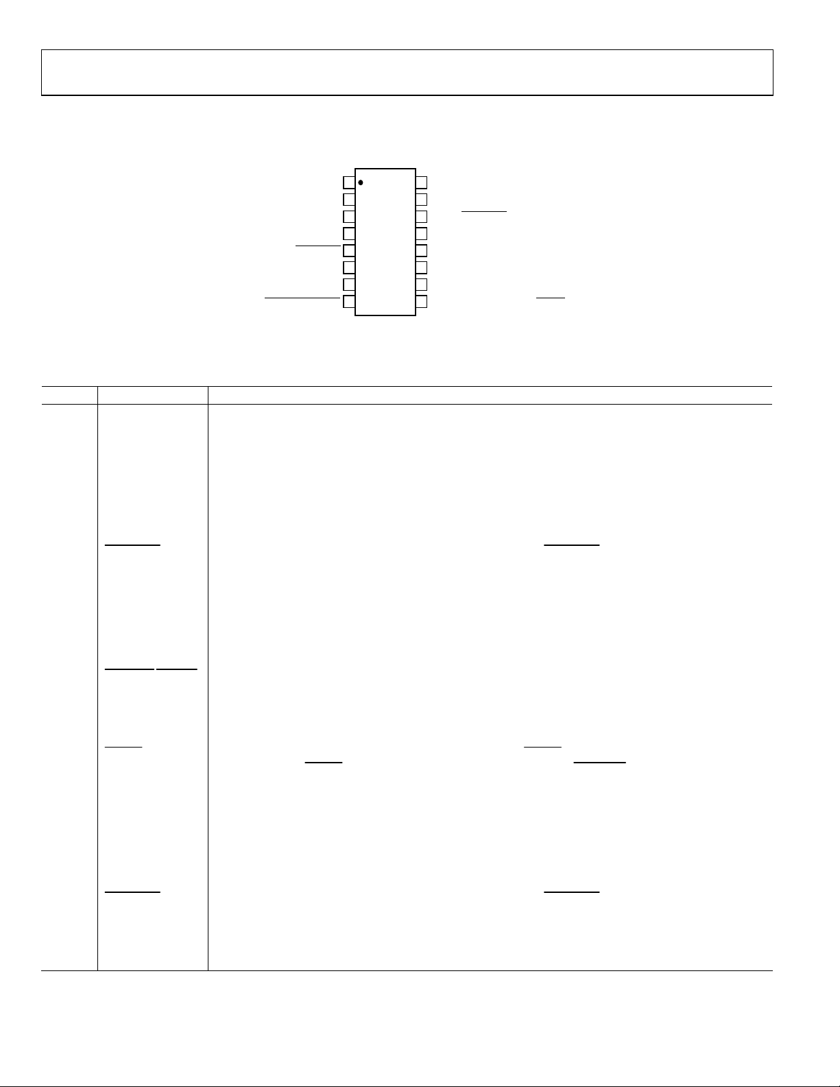
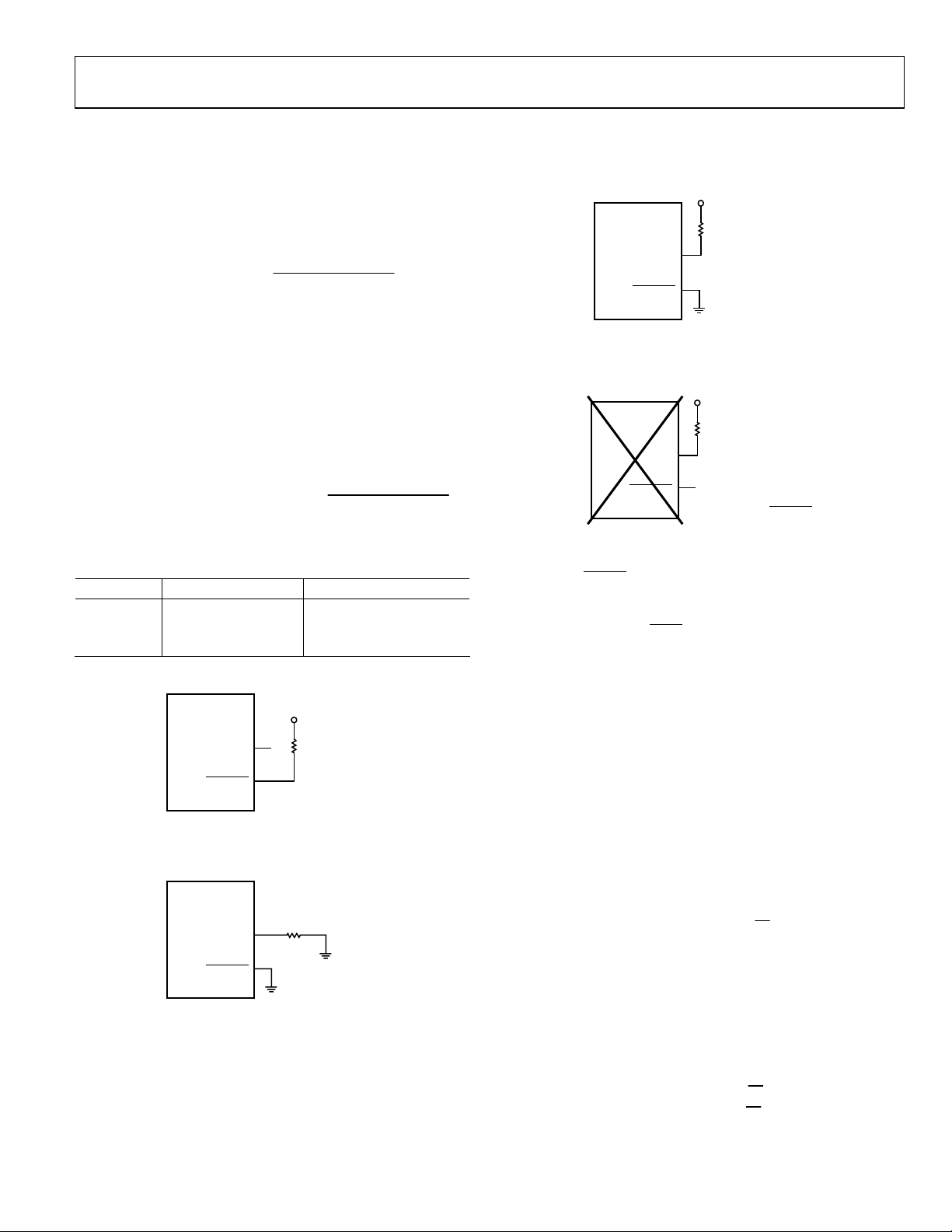
PIN CONFIGURATION AND FUNCTION DESCRIPTIONS
SCL
GND
V
TACH3
2/SMBALERT
PWM
TACH1
TACH2
PWM3/ADDRESS ENABLE
CC
1
2
3
ADT7460
4
TOP VIEW
(Not to Scale)
5
6
7
8
SDA
16
PWM1/XTO
15
/SMBALERT
+2.5V
14
IN
13
D1+
12
D1–
11
D2+
10
D2–
9
TACH4/ADDRESS SELECT/THERM
03228-003
Figure 3. Pin Configuration
Table 3. P tion Descript
Pin No. Mnemonic
in Func ions
Description
1 SCL Digital Input (Open Drain). SMBus serial clock input. Requires SMBus pull-up.
2 GND 460. Ground Pin for the ADT7
3 V
CC
Power Supply. Can be powered by 3.3 V standby if monitoring in low power states is required. VCC is also
monitored through this pin. The ADT7460 can also be powered from a 5 V supply. Setting Bit 7 of
Configuration Register 1 (Reg. 0x40) rescales the V
4 TACH3
input attenuators to correctly measure a 5 V supply.
CC
re speed of Fan 3. Can be reconfigured as an Digital Input (Open Drain). Fan tachometer input to measu
analog input (AIN3) to measure the speed of 2-wire fans.
5 PWM2
Digital O
utput (Open Drain). Requires 10 kΩ typical pull-up. Pulse-width modulated output to control
Fan 2 speed.
SMBALERT
Digital Output (Open Drain). This pin may be reconfigured as an SMBALERT interrupt output to signal
out-of-limit conditions.
6 TACH1
re speed of Fan 1. Can be reconfigured as an Digital Input (Open Drain). Fan tachometer input to measu
analog input (AIN1) to measure the speed of 2-wire fans.
7 TACH2
Digital Input (Open Drain). Fan tachometer input to measure speed of Fan 2. Can be reconfigured as an
analog input (AIN2) to measure the speed of 2-wire fans.
8 PWM3
pull-up.
ADDRESS ENABLE If pulled low on power-up, this places the ADT7460 into address select mode, and the state of Pin 9
determines the ADT7460’s slave address.
9 TACH4
put to measure speed of Fan 4. Can be reconfigured as an Digital Input (Open Drain). Fan tachometer in
analog input (AIN4) to measure the speed of 2-wire fans.
ADDRESS SELECT If in address select mode, this pin determines the SMBus device address.
THERM Alternatively, the pin may be reconfigured as a bidirectional THERM pin. Can be used to time and monit
assertions on the
THERM input. For example, can be connected to the PROCHOT output of Intel’s Pentium 4
processor or to the output of a trip point temperature sensor. Can be used as an output to signal
overtemperature conditions.
10 D2− Cathode Connection to Second Thermal Diode.
11 D2+ Anode Connection to Second Thermal Diode.
12 D1− Cathode Connection to First Thermal Diode.
13 D1+ Anode Connection to First Thermal Diode.
14 +2.5V
SMBALERT Digital Output (Open Drain). This pin may be reconfigured as an SMBALERT interrupt output to signal
IN
Analog Input. Monitors 2.5 V supply, typically a chipset voltage.
out-of-limit conditions.
15 PWM1/XTO
Digital Output (Open Drain). Pulse-width modulated output to control Fan 1 speed. Requires 10 kΩ typical
pull-up.
16 SDA Digital I/O (Open Drain). SMBus bidirectional serial data. Requires SMBus pull-up.
ypical Digital I/O (Open Drain). Pulse-width modulated output to control Fan 3/4 speed. Requires 10 kΩ t
or
Rev. C | Page 6 of 52
ADT7460
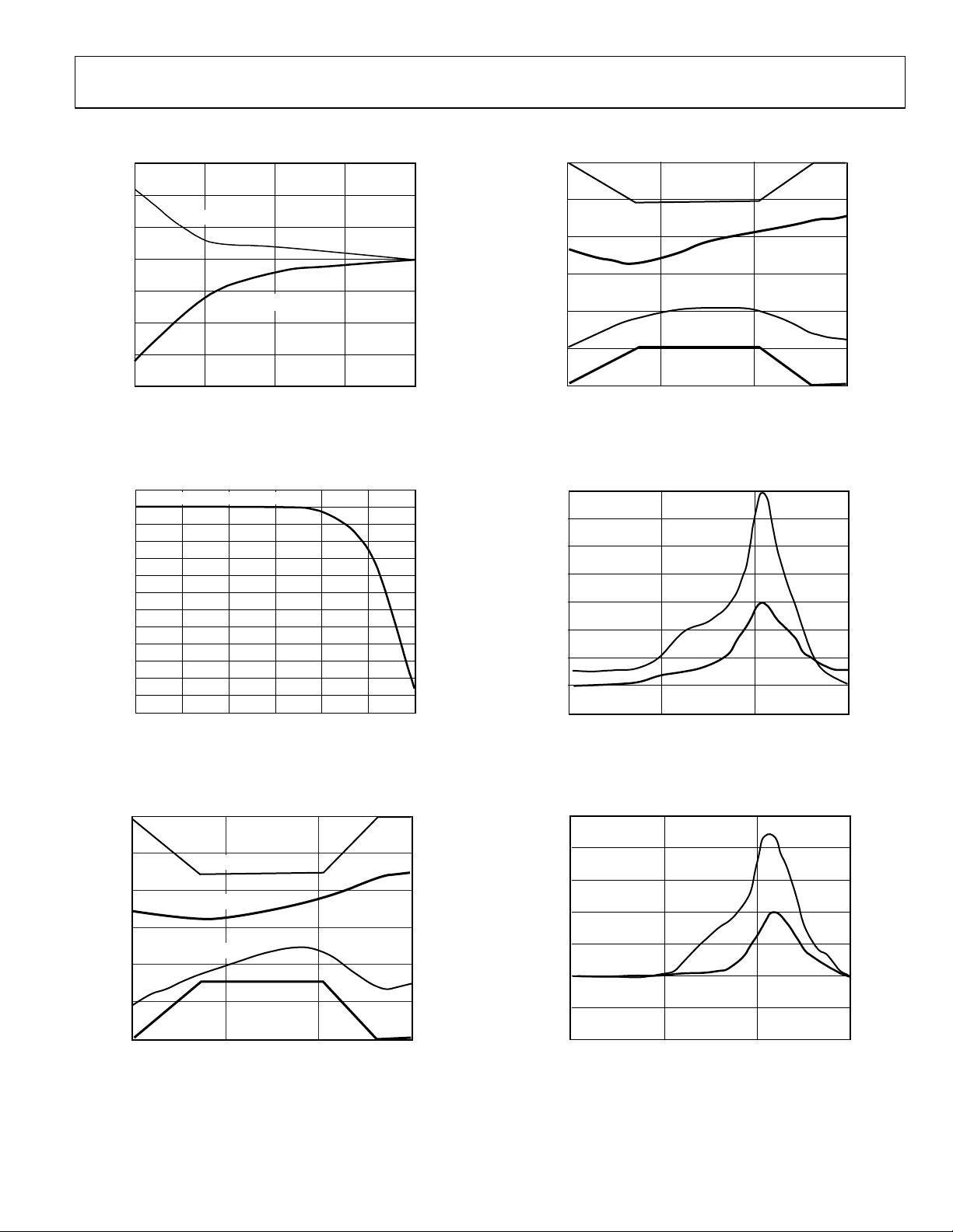
TYPICAL PERFORMANCE CHARACTERISTICS
15
3
10
5
0
–5
–10
–15
REMOTE TEMPERATURE ERROR (°C)
–20
1 3.3 100.0
DXPTO GND
DXP TO VCC(3.3V)
LEAKAGE RESISTANCE (MΩ)
10.0 30.0
Figure 4. Remote Temperature Error vs. Leakage Resistance
3
REMOTE TEMPERATURE ERROR (°C)
0
–3
–6
–9
–12
–15
–18
–21
–24
–27
–30
REMOTE TEMPERATURE ERROR (°C)
–33
–36
1
2.2 3.3 4.7 10.0 22.0 47.0
DXP–DXN CAPACITANCE (nF)
Figure 5. Remote Temperature Error vs. Capacitance between D+ and D−
03228-004
03228-005
2
1
0
–1
–2
LOCAL TEMPERATURE ERROR (°C)
–3
–40 10 110
HIGH LIMIT
+3 SIGMA
–3 SIGMA
LOW LIMIT
60
TEMPERATURE (°C)
Figure 7. Local Temperature Error vs. Actual Temperature
14
12
10
8
6
4
2
0
REMOTE TEMPERATURE ERROR (°C)
–2
100k 550k 50M
Figure 8. Remote Temperature Error vs. Power Supply Noise Frequency
250mV
100mV
5M
FREQUENCY (Hz)
03228-007
03228-008
3
2
1
0
–1
–2
REMOTE TEMPERATURE ERROR (°C)
–3
–40
Figure 6. Remote Temperature Error vs. Actual Temperature
HIGH LIMIT
+3 SIGMA
–3 SIGMA
LOW LIMIT
10 60 110
TEMPERATURE (°C)
03228-006
Rev. C | Page 7 of 52
12.5
10.0
7.5
RROR (°C)
E
5.0
2.5
0
LOCAL TEMPERATURE
–2.5
–5.0
100k 550k 50M
250mV
100mV
5M
FREQUENCY (Hz)
Figure 9. Local Temperature Error vs. Power Supply Noise Frequency
03228-009
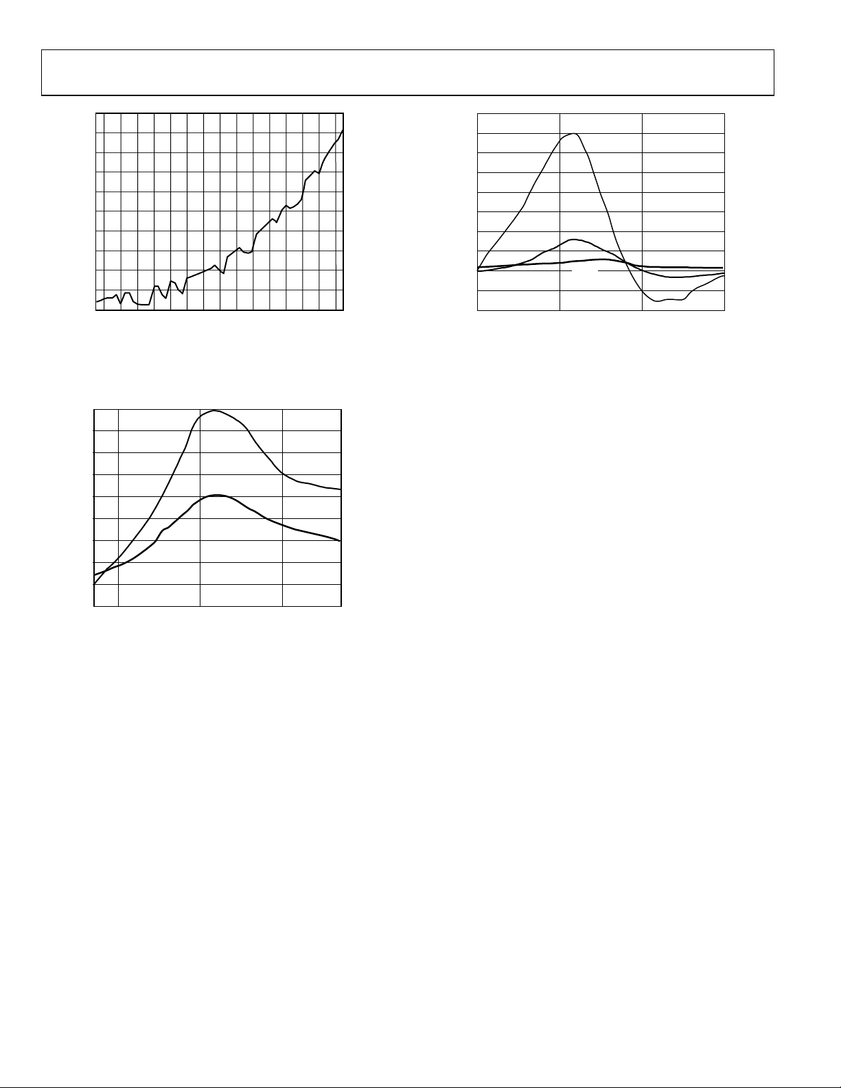
ADT7460
1.90
1.85
1.80
1.75
1.70
1.65
1.60
1.55
SUPPLY CURRENT (mA)
1.50
1.45
1.40
2.6 3.0 3.4 3.8 4.2 4.6 5.0 5.4
2.5
SUPPLYVOLTAGE(V)
Figure 10. Supply Current vs. Supply Voltage
16
14
12
10
8
6
4
2
REMOTE TEMPERATURE ERROR (°C)
0
–2
60k
110k 1M 10M 50M
Figure 11. Remote Temperature Error vs. Differential Mode Noise Frequency
20mV
10mV
FREQUENCY (Hz)
5.5
03228-010
03228-011
40
35
30
25
20
15
10
5
0
REMOTE TEMPERATURE ERROR (°C)
–5
–10
10k
40mV
100mV
20mV
100k 1M 10M
FREQUENCY (Hz)
03228-012
Figure 12. Remote Temperature Error vs. Common-Mode Noise Frequency
Rev. C | Page 8 of 52
ADT7460
PRODUCT DESCRIPTION
The ADT7460 is a thermal monitor and multiple fan controller
for any system requiring monitoring and cooling. The device
communicates with the system via a serial System Management
Bus (SMBus). The serial bus controller has an optional address
line for device selection (Pin 9), a serial data line for reading
and writing addresses and data (Pin 16), and an input line for
the serial clock (Pin 1). All control and programming functions
of the ADT7460 are performed over the serial bus. In addition,
two of the pins can be reconfigured as an
SMBALERT
output to
indicate out-of-limit conditions.
MEASUREMENT INPUTS
The device has three measurement inputs, one for voltage and
two for temperature. It can also measure its own supply voltage
and can measure ambient temperature with its on-chip
temperature sensor.
Pin 14 is an analog input with an on-chip attenuator and is
configured to monitor 2.5 V.
SEQUENTIAL MEASUREMENT
When the ADT7460 monitoring sequence is started, it cycles
sequentially through the measurement of 2.5 V input and the
temperature sensors. Measured values from these inputs are
stored in value registers. These can be read out over the serial
bus or can be compared with programmed limits stored in the
limit registers. The results of out-of-limit comparisons are
stored in the status registers, which can be read over the serial
bus to flag out-of-limit conditions.
RECOMMENDED IMPLEMENTATION
Configuring the ADT7460 as in Figure 13 allows the systems
designer the following features:
• Two PWM outputs for fan control of up to three fans (the
front and rear chassis fans are connected in parallel).
• Three TACH fan speed measurement inputs.
• V
measured internally through Pin 3.
CC
Power is supplied to the chip via Pin 3, and the system also
monitors V
through this pin. In PCs, this pin is normally
CC
connected to a 3.3 V standby supply. This pin can, however, be
connected to a 5 V supply and monitor it without overranging.
Remote temperature sensing is provided by the D1± and D2±
inputs, to which diode-connected, external temperature-sensing
transistors, such as a 2N3904 or CPU thermal diode, may be
connected.
The ADC also accepts input from an on-chip band gap
temperature sensor, which monitors system ambient
temperature.
FRONT
CHASSIS
FAN
REAR
CHASSIS
FAN
AMBIENT
TEMPERATURE
TACH2
PWM3
TACH3
D1+
D1–
ADT7460
• CPU temperature measured using Remote 1 temperature
channel.
• Ambient temperature measured through Remote 2
temperature channel.
• Bidirectional
PROCHOT
overtemperature
•
SMBALERT
P
WM1
TACH1
D2+
D2–
THERM
PROCHOT
THERM
monitoring and can function as an
system interrupt output.
pin. Allows Intel Pentium 4
THERM
output.
SDA
SCL
SMBALERT
GND
Figure 13. Recommended Implementation
Rev. C | Page 9 of 52
ICH
3228-013

ADT7460
ADT7460 AD S SELECTION
Pin 8 is pulled low on p
Pin 9 (T SS SELECT/
ADT7460’s slave addres s high on power-up, the
ADT Bus Slave Address 0x2E. This function
is desc tail later.
Table 4. Summary Inte
Register Description
Configuration These registers provide control and configuration of the ADT7460, including alternate pinout functionality.
Address Pointer
Status Registers
Interrupt Mask
Value and Limit
Offset
T
T
Operating Point
Enhance Acoustics These registers allow each PWM output controlling fan to be tweaked to enhance the system’s acoustics.
ACH4/ADDRE
7460 defaults to SM
ribed in more de
MIN
RANGE
DRES
-functio
n PWMPin 8 is the dual 3/
ADDRESS ENABLE
ower-up, the ADT7460 reads the state of
THERM
) to determine the
pin. If
INTERNAL REGISTERS OF THE ADT7460
Table 4 summarizes the ADT7460’s principal internal registers.
Table 41 to Table 81 describe the registers in more detail.
s. If Pin 8 i
rnal Registers
This register contains the address that selects one of the other internal registers. When writing to the ADT7460, the
first byte of data is always a register address, which is written to the address pointer register.
These registers provide the status of each limit comparison and are used to signal out-of-limit conditions on the
temperature, voltage, or fan speed channels. If Pin 14 or Pin 5 is configured as
whenever an unmasked status bit is set.
These registers allow each interrupt status event to be masked when Pin 14 or Pin 5 is configured as an
output.
The results of analog voltage input, temperature, and fan speed measurements are stored in these registers, along
with their limit values.
These registers allow each temperature channel reading to be offset by a twos complement value written to these
registers.
These registers program the starting temperature for each fan under automatic fan speed control.
These registers program the temperature-to-fan speed control slope in automatic fan speed control mode for each
PWM output.
These registers define the target operating temperatures for each thermal zone when running under dynamic T
control. This function allows the cooling solution to adjust dynamically in response to measured temperature and
system performance.
SMBALERT
, this pin asserts low
SMBALERT
MIN
Rev. C | Page 10 of 52
ADT7460
8
T
-
T
THEORY OF OPERATION
SERIAL BUS INTERFACE
Control of the ADT7460 is carried out using the serial System
Management Bus (SMBus). The ADT7460 is connected to this
bus as a slave device, under the control of a master controller.
The ADT7460 has a 7-bit serial bus address. When the device is
powered up with Pin 8 (PWM3/
ADDRESS ENABLE
ADT7460 has a default SMBus address of 0101110 or 0x2E. If
more than one ADT7460 is to be used in a system, each ADT7460
should be placed in address select mode by strapping Pin 8 low
on power-up. The logic state of Pin 9 then determines the
device’s SMBus address. The logic state of these pins is sampled
on power-up.
The device address is sampled and latched on the first valid
SMBus transaction, more precisely, on the low-to-high
transition at the beginning of the eighth SCL pulse, when the
serial address byte matches the selected slave address. The
selected slave address is chosen using the
ADDRESS ENABLE
/ADDRESS SELECT pins. Any attempted changes in the
address has no effect after this.
Table 5. Address Select Mode
Pin 8 State Pin 9 State Address
0 Low (10 kΩ to GND) 0101100 (0x2C)
0 High (10 kΩ pull-up) 0101101 (0x2D)
1 Don’t Care 0101110 (0x2E) (default)
V
ADT7460
ADDR_SEL
PWM3/ADDR_EN
Figure 14. Default SMBus Address 0x2E
CC
9
8
ADDRESS = 0x2E
10k
Ω
ADT7460
Ω
10k
ADDR_SEL
PWM3/ADDR_EN
Figure 15. SMBus Address 0x2C (Pin 9 = 0)
9
8
ADDRESS = 0x2C
) high, the
03228-014
03228-015
V
CC
ADT7460
ADDR_SEL
PWM3/ADDR_EN
Figure 16. SMBus Address 0x2D (Pin 9 = 1)
ADT7460
ADDR_SEL
PWM3/ADDR_EN
CARE SHOULD BE TAKEN TO ENSURE THAT PIN
(PWM3/ADDR_EN) IS EITHER TIED HIGH OR LOW. LEAVING PIN 8
FLOATING COULD CAUSE THE ADT7460 TO POWER UP WITH AN
UNEXPECTED ADDRESS.
NOTE THAT IF THE ADT7460 IS PLACED INTO ADDRESS SELEC
MODE, PINS 8 AND 9 CAN BE USED AS THE ALTERNATE FUNC
IONS (PWM3, TACH4/THERM) ONLY IF THE CORRECT CIRCUIT IS
MUXED IN AT THE CORRECT TIME.
Figure 17. Unpredictable SMBus Address if Pin 8 is Unconnected
facility to make hardwired changes to the SMBus slav
The e
ess allows the user to avoid conflicts with other devices
addr
shar
ing the same serial bus, for example, if more than one
ADT
7460 is used in a system.
The
serial bus protocol operates as follows:
1.
The master initiates data transfer by establishing a start
10k
Ω
9
8
ADDRESS = 0x2D
V
CC
10kΩ
9
8
NC
DO NOT LEAVE ADDR_EN
UNCONNECTED. C
CAUSE UNPREDIC
ADDRESSES
AN
TABLE
03228-016
condition, defined as a high-to-low transition on the serial
data line SDA while the serial clock line SCL remains high
This indicates that an address/data stream will follow. All
slave peripherals connected to
the serial bus respond to the
star condition and shift in the next eight bits, consisting
a 7-bit address (MSB first) plus a R/
bit, which
W
determine the direction of the data transfer, that is,
whether data is written to or read from the slave device.
The peripheral whose address corresponds to the
transmitted address responds by pulling the data line low
during the low period before the ninth clock pulse, known
as the Acknowledge bit. All other devices on the bus no
remain idle while the selected device
read from or written to it. If the R/
writes to the slave device. If the R/
waits for data to be
bit is a 0, the master
W
bit is a 1, the master
W
reads from the slave device.
03228-017
of
w
.
Rev. C | Page 11 of 52
ADT7460
2.
Data is sent over the serial bus in sequences of nine clock
pulses, eight bits of data followed by an Acknowledge bit
from the slave device. Transitions on the data line must occ
during the low period of the clock signal and remain stable
during the high period, as a low-to-high transition when the
clock is high may be interpreted as a st
op signal. The number
of data bytes that can be transmitted over the serial bus in a
single read or write operation is limited only by what the
master and slave devices can handle.
3. When all data bytes have been read or written, stop conditio
are established. In write
mode, the master pulls the data line
high during the 10th clock pulse to assert a stop condition. In
read mode, the master device overrides the acknowledge bit
by pulling the data line high during the low period
before the
ninth clock pulse. This is known as No Acknowledge. The
master then takes the data line low during the low period
before the 10th clock pulse, then high during the 10th clock
pulse to assert a stop condition.
Any number of bytes of data may be transferred over the serial
bus in one operation, but it is not possible to mix read and write
in one operation because the type of operation is determined at
1
SCL
ur
ns
the beginning and cannot subsequently be changed without
starting a new operation.
In the case of the ADT7460, write operations contain either one
or two bytes, and read operations contain one byte.
To write data to one of the device data re
gisters or read data
from it, the address pointer register must be set so that the
correct data register is addressed. Then data can be written in
that register or read from it. The first byte of a write operation
always contains an address that is stored in the address pointer
register. If data is to be written to the device, the write operation
contains a second data byte that is written to the register
selected by the addres
This is i
llustrated in Figure 18. The device address is sent over
the bus followed by R/
s pointer register.
being set to 0. This is followed by two
W
data bytes. The first data byte is the address of the internal data
register to be written to, which is stored in the address pointer
register. The second data byte is the data to be written to the
internal data register.
1
9
9
SDA
START BY
MASTER
0
0
1
SERIAL BUS ADDRESS
1
1
FRAME 1
BYTE
SDA (CONTINUED)
A0
A1
SCL (CONTINUED)
R/W
ACK. BY
ADT7460
1
D7
D6
D7
ADDRESS POINTER REGISTER BYTE
D5
D6
D5
D4
D4
D3
FRAME 3
DATA
BYTE
FRAME 2
D2
D3
D2
D1
D0
ACK. BY
ADT7460
9
D1
D0
ACK. BY
ADT7460
STOP BY
MASTER
03228-018
Figure 18. Writing a Register Address to the Address Pointer Register, Then Writing Data to the Selected Register
Rev. C | Page 12 of 52
ADT7460
When reading data from a register, there are two possibilities:
• If the ADT7460’s address pointer register value is unknown
or not the desired value, it is first necessary to set it to the
correct value before data can be read from the desired data
register. This is done by performing a write to the ADT7460
as before, but only the data byte containing the register
address is sent because data is not to be written to the
register. This is shown in Figure 19.
A read operation is then performed, consisting of the serial
bus address, R/
bit set to 1, followed by the data byte
W
read from the data register. This is shown in Figure 20.
• If the address pointer register is known to be already at the
desired address, data can be read from the corresponding
data register without first writing to the address pointer
register, so Figure 19 can be omitted.
It is possible to read a data byte from a data register without first
writing to the address pointer register if the address pointer
register is already at the correct value. However, it is not possible
to write data to a register without writing to the address pointer
register because the first data byte of a write is always written to
the address pointer register.
In Figure 18 to Figure 20, the serial bus address is shown as the
default value 01011(A1)(A0), where A1 and A0 are set by the
address select mode function previously defined.
In addition to supporting the Send Byte and Receive Byte
protocols, the ADT7460 also supports the Read Byte protocol
(see System Management Bus specifications Rev. 2.0 for more
information).
1
SCL
9
If it is required to perform several read or write operations in
succession, the master can send a repeat start condition instead
of a stop condition to begin a new operation.
Write Operations
The SMBus specification defines several protocols for different
types of read and write operations. The ones used in the
ADT7460 are discussed below. The following abbreviations are
used in the diagrams:
S—start
P—sto p
R—read
W—wr it e
A—ack nowledge
—no acknowledge
A
The ADT7460 uses the following SMBus write protocols:
Send Byte
In this operation, the master device sends a single command
byte to a slave device as follows:
1. The master device asserts a start condition on SDA.
2. The master sends the 7-bit slave address followed by the
write bit (low).
3. The addressed slave device asserts ACK on SDA.
4. The master sends the register address.
5. The slave asserts ACK on SDA.
6. The master asserts a stop condition on SDA and the
transaction ends.
1
9
SDA
START BY
MASTER
0
10
SERIAL BUS ADDRESS
1
FRAME 1
BYTE
D6
1
A0
A1
R/W
ACK. BY
ADT7460
D7
D4
D5
ADDRESS POINTER REGISTER BYTE
D3
FRAME 2
D2
D1
D0
ACK. BY
ADT7460
STOP BY
MASTER
03228-019
Figure 19. Writing to the Address Pointer Register Only
D0
NO ACK. BY
MASTER
9
STOP BY
MASTER
03228-020
1
SCL
0
SDA
START BY
MASTER
1011
FRAME 1
SERIAL BUS ADDRESS
BYTE
A0
A1
Figure 20. Read
9
1
D6
W
R/
ACK
. BY
ADT7460
D7
D4
D5
FRAME 2
DATA BYTE FROM ADT7460
ing Data from a Previously Selec ted Register
Rev. C | Page 13 of 52
D3
D2
D1

ADT7460
7460, the send byte protocol is used to write to the For the ADT
address pointer register for a subsequent single-byte read from
the same address. This is illustrated in Figure 21.
231564
SLAVE
ADDRESS ADDRESS
Figure 21. Settin
ely after
If it is required to read data from the register immediat
tin art
set g up the address, the master can assert a repeat st
d nd carry out a
con ition immediately after the final ACK a
g a Register Address for Subsequent Read
single-byte read without asserting an intermediate stop
d
con ition.
i
Wr te Byt e
h ends a command byte and
In t is operation, the master device s
one data byte to the slave device as follows:
1. evice asserts a start condition on SDA.
The master d
2. The master sends the 7-bit
write bit (low).
3. The addressed slave device asserts ACK on SDA.
4. The maste
5. The slave assert
r sends the register address.
s ACK on SDA.
REGISTER
WASAP
03228-021
slave address followed by the
3. The addressed slave de
vice asserts ACK on SDA.
4. The master receives a data byte.
5. The master asserts NO ACK on SD
A.
6. The master asserts a stop condition on SDA and the
transaction ends.
In the ADT7460, the receive byte protocol is used to read a
single byte of data from a register whose address has previously
been set by
a send byte or by write byte operation.
213564
SLAVE
SWA AP
ADDRESS
Figure 23. Single-Byte Read from a Register
REGISTER
ADDRESS
03228-023
Alert Response Address
r t
Ale t response address (ARA) is a feature of SMBus devices tha
allow
s an interrupting device to identify itself to the host when
mul
tiple devices exist on the same bus.
The
SMBALERT
can be used as an
ected to a common conn
ter. If a device’s
mas
output can be used as an interrupt output or
SMBALERT
SMBALERT
. One or more outputs can be
SMBALERT
line connected to
line goes low, the following
the
occurs:
6. The master sends a data byte.
7. The slave
asserts ACK on SDA.
8. The master asserts a stop condition on SDA to end the
transaction.
This is illustrated i
n Figure 22.
24653178
SLAVE
ADDRESS ADDRESS
Figure
REGISTER
22. Single-Byte Write to a Register
DATAAAWSAP
03228-022
Read Operations
The ADT7460 uses the following SMB
e
Rec ive Byte
This is useful when repeatedly reading a single register. Th
regis have been set up previously. In this
ter address needs to
us read protocols.
e
operation, the master device receives a single byte from a slave
device as follows:
1. The master device asserts a start condition on SD
2. The master sends the 7-bit ave address followed by the
read bit (
high).
sl
A.
1.
SMBALERT
is pulled low.
Master2. initiates a read operation and sends the alert
response address (ARA = 0001 100). This is a general call
address, which must not be used as a specific device
address.
3. The device whose
SMBALERT
output is low responds to
the alert response address, and the master reads its device
address. The address of the device is now known, and it
can be interrogated in the usual way.
4. If more than one device’s
SMBALERT
output is low, the
one with the lowest device address has priority in
accordance with normal SMBus arbitration.
5. Once the ADT7460 has responded to the alert response
address, the master must read the status registers and the
SMBALERT
is cleared only if the error condition has gone
away.
Rev. C | Page 14 of 52
ADT7460
SMBus Timeout
The ADT7460 includes an SMBus timeout feature. If there is no
SMBus activity for 25 ms, the ADT7460 assumes that the bus is
locked and releases the bus. This prevents the device from
locking or holding the SMBus expecting data. Some SMBus
controllers cannot handle the SMBus timeout feature, so it can
be disabled.
Table 6. Configuration Register 1 (Reg. 0x40)
Bit Description
<6> TODIS 0: SMBus timeout enabled (default)
<6> TODIS 1: SMBus timeout disabled
VOLTAGE MEASUREMENT INPUT
The ADT7460 has one external voltage measurement channel.
It can also measure its own supply voltage, V
Pin 14 may be configured to measure a 2.5 V supply. The V
supply voltage measurement is carried out through the V
(Pin 3). Setting Bit 7 of Configuration Register 1 (Reg. 0x40)
allows a 5 V supply to power the ADT7460 and be measured
without overranging the V
measurement channel. The 2.5 V
CC
input can be used to monitor a chipset supply voltage in
computer systems.
Analog-to-Digital Converter
All analog inputs are multiplexed into the on-chip, successive
approximation, analog-to-digital converter. This has a resolution
of 10 bits. The basic input range is 0 V to 2.25 V, but the input
has built-in attenuators to allow measurement of 2.5 V without
any external components. To allow the tolerance of the supply
voltage, the ADC produces an output of 3/4 full scale (768d or
0x300) for the nominal input voltage and so has adequate
headroom to deal with overvoltages.
.
CC
CC
pin
CC
Input Circuitry
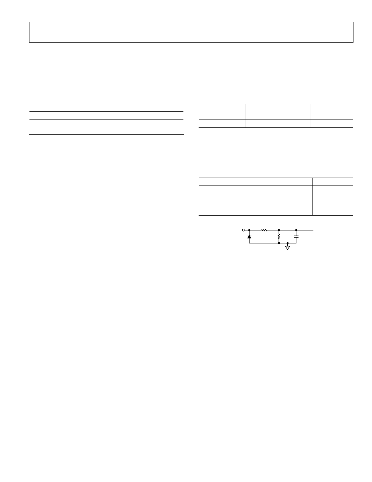
The internal structure for the 2.5 V analog input is shown in
Figure 24. The input circuit consists of an input protection
diode, an attenuator, plus a capacitor to form a first-order lowpass filter that gives the input immunity to high frequency
noise.
Table 7. Voltage Measurement Registers
Register Description Default
0x20 2.5 V reading 0x00
0x22 VCC reading 0x00
Associated with the voltage measurement channels are a high
and low limit register. Exceeding the programmed high or low
limit causes the appropriate status bit to be set. Exceeding either
limit can also generate
SMBALERT
interrupts.
Table 8. 2.5 V Limit Registers
Register Description Default
0x44 2.5 V low limit 0x00
0x45 2.5 V high limit 0xFF
0x48 VCC low limit 0x00
0x49 VCC high limit 0xFF
2.5V
IN
Figure 24. Structure of Analog Inputs
45kΩ
94kΩ 30pF
03228-024
Table 9 shows the input ranges of the analog inputs and output
codes of the 10-bit ADC.
When the ADC is running, it samples and converts a voltage
input in 711 µs and averages 16 conversions to reduce noise; a
measurement takes nominally 11.38 ms.
Rev. C | Page 15 of 52

ADT7460
Table 9. 10-Bit A/D Output Code vs. V
5 V
IN
VCC (3.3 VIN)
<0.0065 <0.0042 <0.0032 0 00000000 00
0.0065–0.0130 0.0042–0.0085 0.0032–0.0065 1 00000000 01
0.0130–0.0195 0.0085–0.0128 0.0065–0.0097 2 00000000 10
0.0195–0.0260 0.0128–0.0171 0.0097–0.0130 3 00000000 11
0.0260–0.0325 0.0171–0.0214 0.0130–0.0162 4 00000001 00
0.0325–0.0390 0.0214–0.0257 0.0162–0.0195 5 00000001 01
0.0390–0.0455 0.0257–0.0300 0.0195–0.0227 6 00000001 10
0.0455–0.0521 0.0300–0.0343 0.0227–0.0260 7 00000001 11
0.0521–0.0586 0.0343–0.0386 0.0260–0.0292 8 00000010 00
• • • • •
• • • • •
• • • • •
1.6675–1.6740 1.1000–1.1042 0.8325–0.8357 256 (1/4 scale) 01000000 00
• • • • •
• • • • •
• • • • •
3.3300–3.3415 2.2000–2.2042 1.6650–1.6682 512 (1/2 scale) 10000000 00
• • • • •
• • • • •
• • • • •
5.0025–5.0090 3.3000–3.3042 2.4975–2.5007 768 (3/4 scale) 11000000 00
• • • • •
• • • • •
• • • • •
6.5983–6.6048 4.3527–4.3570 3.2942–3.2974 1013 11111101 01
6.6048–6.6113 4.3570–4.3613 3.2974–3.3007 1014 11111101 10
6.6113–6.6178 4.3613–4.3656 3.3007–3.3039 1015 11111101 11
6.6178–6.6244 4.3656–4.3699 3.3039–3.3072 1016 11111110 00
6.6244–6.6309 4.3699–4.3742 3.3072–3.3104 1017 11111110 01
6.6309–6.6374 4.3742–4.3785 3.3104–3.3137 1018 11111110 10
6.6374–6.4390 4.3785–4.3828 3.3137–3.3169 1019 11111110 11
6.6439–6.6504 4.3828–4.3871 3.3169v3.3202 1020 11111111 00
6.6504–6.6569 4.3871–4.3914 3.3202–3.3234 1021 11111111 01
6.6569–6.6634 4.3914–4.3957 3.3234–3.3267 1022 11111111 10
>6.6634 >4.3957 >3.3267 1023 11111111 11
1
The VCC output codes listed assume that VCC is 3.3 V. If VCC input is reconfigured for 5 V operation (by setting Bit 7 of Configuration Register 1), the VCC output codes are
the same as for the 5 V
column.
IN
IN
Input Voltage A/D Output
1
2.5 V
IN
Decimal Binary (10 Bits)
Rev. C | Page 16 of 52

ADT7460
(
ADDITIONAL ADC FUNCTIONS FOR VOLTAGE MEASUREMENTS
A number of other functions are available on the ADT7460 to
offer the systems designer increased flexibility.
Turn-Off Averaging
For each voltage measurement read from a value register, 16
readings have actually been made internally and the results
averaged before being placed into the value register. If the user
wants to speed up conversion, setting Bit 4 of Configuration
Register 2 (Reg. 0x73) turns averaging off. This effectively gives
a reading 16 times faster (711 µs), but the reading may be noisier.
Bypass Voltage Input Attenuator
Setting Bit 5 of Configuration Register 2 (Reg. 0x73) removes
the attenuation circuitry from the 2.5 V input. This allows the
user to directly connect external sensors or to rescale the analog
voltage measurement inputs for other applications. The input
range of the ADC without the attenuators is 0 V to 2.25 V.
Single-Channel ADC Conversion
Setting Bit 6 of Configuration Register 2 (Reg. 0x73) places the
ADT7460 into single-channel ADC conversion mode. In this
mode, the ADT7460 can be made to read a single voltage
channel only. If the internal ADT7460 clock is used, the selected
input is read every 711 µs. The appropriate ADC channel is
selected by writing to Bits <7:5> of the TACH1 Minimum High
Byte register (Reg. 0x55).
Table 10. Configuration Register 2 (Reg. 0x73)
Bit Description
<4> 1: averaging off
<5> 1: bypass input attenuators
<6> 1: single-channel convert mode
Table 11. TACH1 Minimum High Byte (Reg. 0x55)
Bit Description
<7:5> Selects ADC channel for single-channel convert mode
Value Channel Selected
000 2.5 V
010 V
CC
TEMPERATURE MEASUREMENT SYSTEM
Local Temperature Measurement
The ADT7460 contains an on-chip band gap temperature
sensor whose output is digitized by the on-chip 10-bit ADC.
The 8-bit MSB temperature data is stored in the local
temperature register (Address 0x26). As both positive and
negative temperatures can be measured, the temperature data is
stored in twos complement format, as shown in Table 12.
Theoretically, the temperature sensor and ADC can measure
temperatures from −128°C to +127°C with a resolution of
0.25°C. However, this exceeds the operating temperature range
of the device, so local temperature measurements outside this
range are not possible.
Remote Temperature Measurement
The ADT7460 can measure the temperature of two remote
diode sensors or diode-connected transistors connected to
Pins 12 and 13, or Pins 10 and 11.
The forward voltage of a diode or diode-connected transistor
operated at a constant current exhibits a negative temperature
coefficient of about −2 mV/°C. Unfortunately, the absolute
value of V
calibration is required to null this out, so the technique is
unsuitable for mass production. The technique used in the
ADT7460 is to measure the change in V
operated at two different currents. This is given by
where:
K is Boltzmann’s constant.
q is the charge on the carrier.
T is the absolute temperature in Kelvins.
N is the ratio of the two currents.
Figure 25 shows the input signal conditioning used to measure
the output of a remote temperature sensor. This figure shows
the external sensor as a substrate transistor provided for
temperature monitoring on some microprocessors. It could
equally well be a discrete transistor, such as a 2N3904.
varies from device to device, and individual
BE
when the device is
BE
)
NInqKTV
BE
×=∆
V
IN× II
CPU
THERMDA
REMOTE
SENSING
TRANSISTOR
THERMDC
Figure 25. Signal Conditioning for Remote Diode Temperature Sensors
D+
D–
BIAS
DIODE
Rev. C | Page 17 of 52
BIAS
fC = 65kHz
LPF
DD
V
OUT+
TO ADC
V
OUT–
03228-025

ADT7460
If a discrete transistor is used, the collector is not grounded, and
it should be linked to the base. If a PNP transistor is used, the
base is connected to the D− input and the emitter to the D+
input. If an NPN transistor is used, the emitter is connected to
the D− input, and the base to the D+ input. Figure 26 and
Figure 27 show how to connect the ADT7460 to an NPN or
PNP transistor for temperature measurement. To prevent
ground noise from interfering with the measurement, the more
negative terminal of the sensor is not referenced to ground but
is biased above ground by an internal diode at the D− input.
To me asu re Δ V
currents of I and N × I. The resulting waveform is passed
through a 65 kHz low-pass filter to remove noise and to a
chopper stabilized amplifier that performs the functions of
amplification and rectification of the waveform to produce a dc
voltage proportional to ΔV
ADC to give a temperature output in 10-bit, twos complement
format. To further reduce the effects of noise, digital filtering is
performed by averaging the results of 16 measurement cycles. A
remote temperature measurement takes nominally 25.5 ms. The
results of remote temperature measurements are stored in
10-bit, twos complement format, as illustrated in Table 12. The
extra resolution for the temperature measurements is held in
the Extended Resolution Register 2 (Reg. 0x77). This gives
temperature readings with a resolution of 0.25°C.
Figure 26. Measuring Temperature by Using an NPN Transistor
Figure 27. Measuring Temperature by Using a PNP Transistor
, the sensor is switched between operating
BE
. This voltage is measured by the
BE
ADT7460
2N3904
NPN
2N3906
PNP
D+
D–
ADT7460
D+
D–
03228-026
03228-027
Table 12. Temperature Data Format
Temperature Digital Output (10-Bit)
−128°C
−125°C
−100°C
−75°C
−50°C
−25°C
−10°C
0°C
+10.25°C
+25.5°C
+50.75°C
+75°C
+100°C
+125°C
+127°C
1
Bold denotes 2 LSBs of measurement in the Extended Resolution Register 2
(Reg. 0x77) with 0.25°C resolution.
1000 0000 00
1000 0011 00
1001 1100 00
1011 0101 00
1100 1110 00
1110 0111 00
1111 0110 00
0000 0000 00
0000 1010 01
0001 1001 10
0011 0010 11
0100 1011 00
0110 0100 00
0111 1101 00
0111 1111 00
1
Table 13. Temperature Measurement Registers
Register Description Default
0x25 Remote 1 temperature 0x80
0x26 Local temperature 0x80
0x27 Remote 2 temperature 0x80
0x77 Extended Resolution 2 0x00
Table 14. Extended Resolution Temperature Measurement
Register Bits (Addr = 0x77)
Bit Mnemonic Description
<7:6> TDM2 Remote 2 temperature LSBs
<5:4> LTMP Local temperature LSBs
<3:2> TDM1 Remote 1 temperature LSBs
Reading Temperature from the ADT7460
It is important to note that temperature can be read from the
ADT7460 as an 8-bit value (with 1°C resolution) or as a 10-bit
value (with 0.25 C resolution). If only 1°C resolution is required,
the temperature readings can be read back at any time and in no
particular order.
If the 10-bit measurement is required, this involves a 2-register
read for each measurement. The extended resolution register
(Reg. 0x77) should be read first. This causes all temperature
reading registers to be frozen until all temperature reading
registers have been read from. This prevents an MSB reading
from being updated while its two LSBs are being read, and vice
versa.
Rev. C | Page 18 of 52

ADT7460
Nulling Out Temperature Errors
As CPUs run faster, it becomes more difficult to avoid high
frequency clocks when routing the D+, D− traces around a
system board. Even when recommended layout guidelines are
followed, there may still be temperature errors attributed to
noise being coupled onto the D+/D− lines. High frequency
noise generally has the effect of giving temperature measurements that are too high by a constant amount. The ADT7460
has temperature offset registers at Addresses 0x70, 0x72 for the
Remote 1 and Remote 2 temperature channels. By doing a onetime calibration of the system, one can determine the offset
caused by system board noise and null it out using the offset
registers. The offset registers automatically add a twos
complement 8-bit reading to every temperature measurement.
The LSB adds 0.25°C offset to the temperature reading so the
8-bit register effectively allows temperature offsets of up to
±32°C with a resolution of 0.25°C. This ensures that the
readings in the temperature measurement registers are as
accurate as possible.
Table 15. Temperature Offset Registers
Register Description Default
0x70 Remote 1 temperature offset 0x00 (0°C)
0x71 Local temperature offset 0x00 (0°C)
0x72 Remote 2 temperature offset 0x00 (0°C)
Temperature Measurement Limit Registers
Associated with each temperature measurement channel are
high and low limit registers. Exceeding the programmed high or
low limit causes the appropriate status bit to be set. Exceeding
either limit can also generate
SMBALERT
interrupts.
Table 16. Temperature Measurement Limit Registers
Register Description Default
0x4E Remote 1 temperature low limit 0x81
0x4F Remote 1 temperature high limit 0x7F
0x50 Local temperature low limit 0x81
0x51 Local temperature high limit 0x7F
0x52 Remote 2 temperature low limit 0x81
0x53 Remote 2 temperature high limit 0x7F
Overtemperature Events
Overtemperature events on any of the temperature channels can
be detected and dealt with automatically in automatic fan speed
control mode. Registers 0x6A to 0x6C are the
When a temperature exceeds its
THERM
limit, all fans run at
THERM
limits.
100% duty cycle. The fans continue running at 100% until the
temperature drops below
THERM
– Hysteresis. (This can be
disabled by setting the BOOST bit in Configuration Register 3,
Bit 2, Register 0x78). The hysteresis value for that
THERM
limit
is the value programmed into Registers 0x6D and 0x6E
(hysteresis registers). The default hysteresis value is 4°C.
THERM LIMIT
HYSTERESIS = (°C)
TEMPERATURE
FANS
Figure 28.
100%
THERM
Limit Operation
ADDITIONAL ADC FUNCTIONS FOR TEMPERATURE MEASUREMENT
A number of other functions are available on the ADT7460 to
offer the systems designer increased flexibility:
Turn-Off Averaging
For each temperature measurement read from a value register,
16 readings have actually been made internally and the results
averaged before being placed into the value register. Sometimes
it may be necessary to take a very fast measurement, for
example, of CPU temperature. Setting Bit 4 of Configurat
Register 2 (Re
every 15.5 ms. Each remote temperature measurem
4 ms and the local temperature measurement take
e-Ch versions
Singl annel ADC Con
g Bit eg. 0x73) places the
Settin 6 of Configuration Register 2 (R
DT7460 into single-channel ADC conversion mode. In this
A
ode, the ADT7460 can be made to read a single temperature
m
g. 0x73) turns averaging off. This takes a reading
ent takes
s 1.4 ms.
channel only. The appropriate ADC channel is selected b
its < CH1 minimum high byte register
to B 7:5> of the TA
x
(Reg. 0 55).
17 iguration Register 2 (
Table . Conf Reg. 0x73)
Bit Description
<4> 1: Averaging off
<6> 1: single-channel convert mode
Table 18. TACH1 Minimum High Byte (Reg. 0x55)
it Description B
<7:5> Selects ADC channel for single-channel convert mode
Value Channel Selected
101 Remote 1 temp
110 Local temp
111 Remote 2 temp
ion
y writing
03228-028
Rev. C | Page 19 of 52

ADT7460
LIMITS, STATUS REGISTERS,
Limit Val
Associ ch measuremen
are hig mits. These can fo system
status a status bit can b -of-lim
condit cted by polling atively
SM
microcontroller of out-of-limit conditions
8-Bit Lim
The fo a list of 8-bit limits on the ADT74 0.
Table 19. Volta it Registers
Regist Description Defau
0x44 2.5 V low limit 0x00
0x45 2.5 V high limit 0xFF
0x48 VCC low limit 0x00
0x49 VCC high limit 0xFF
Table 20. Temp e Limit Registers
Regist Description Defau
0x4E Remote 1 temperature low limit 0x81
0x4F
0x6A
0x50 Local temperature low limit 0x81
0x51 Local temperature high limit 0x7F
0x6B
0x52 Remote 2 temperature low limit 0x81
0x53
0x6C
Table 21.
Register Description Default
0x7A
16-Bit Limits
The fan measurements are 16-bit res n TA
limits a
Since f
condit terest, only high limits exist fo CHs.
Since fa period is actually being me
the limit indicates a slow or stalled
ues
ated with ea t channel on the ADT7460
h and low li rm the basis of
monitoring: e set for any out it
ion and dete the device. Altern ,
BALERT
interrupts can be generated to flag a processor or
its
llowing is 6
ge Lim
er lt
eratur
er lt
Remote 1 temperature high
limit
Remote 1
Local
Remote 2 temperature high
limit
Remote 2
THERM
THERM timer limit
THERM limit
THERM limit
THERM limit
Timer Limit Register
TACH ults. The fa CH
re also 1 yte and lo .
ans run re norma nly
6 bits, consisting of a high b
ning under speed or stalled a
ions of in r fan TA
n TACH asured, ex g
AND INTERRUPTS
.
0x7F
0x64
0x64
0x7F
0x64
0x00
w byte
lly the o
ceedin
fan.
Out-of-Limit Comparisons
Once all limits have been programmed, the ADT7460 can be
enabled for monitoring. The ADT7460 measures all parameters
in round-robin format and sets the appropriate status bit for
out-of-limit conditions. Comparisons are done differently
depending on whether the measured value is being compared to
a high or low limit.
• High limit: > comparison performed
• Low limit: < or = comparison performed
NO INT
LOW LIMIT
TEMP > LOW LIMIT
Figure 29. Temperature > Low Limit: No
INT
INT
LOW LIMIT
03228-029
Table 22. Fan Limit Registers
Register Description Default
0x54 TACH1 minimum low byte 0xFF
0x55 TACH1 minimum high byte 0xFF
0x56 TACH2 minimum low byte 0xFF
0x57 TACH2 minimum high byte 0xFF
0x58 TACH3 minimum low byte 0xFF
0x59 TACH3 minimum high byte 0xFF
0x5A TACH4 minimum low byte 0xFF
0x5B TACH4 minimum high byte 0xFF
Rev. C | Page 20 of 52
Figure 30. Temperature = Low Limit:
TEMP = LOW LIMIT
INT
Occurs
03228-030

ADT7460
The total number of channels measured is
NO INT
HIGH LIMIT
Figure 31. Temperature = High Limit: No
INT
HIGH LIMIT
TEMP = HIGH LIMIT
INT
03228-031
• Two supply voltage inputs (2.5 V and V
• Local temperature
• Two remote temperatures
As mentioned previously, the ADC performs round-robin
conversions and take age measurement,
s 11.38 ms for each volt
12 ms for a local temperature reading, an
ote rea
rem temperature ding.
e tot toring cy
Th al moni cle time for averaged voltage and
per monitorin
tem ature g is, therefore, nominally
(2 × 11.38) + 12 (2
e round robin starts s
Th again 35 ms later. Therefore, all channel
eas pproxim
Fan TACH measureme
synchronized with the a urements in any way.
ATU GISTER
ST S RE S
esults of limit com us Registers 1
and 2. Th
he la asuremen l.
of t
tus register b us
e sta
st me
If a measurement is with g status
gister bit is cleared to 0. If the measurement is out-of-limits,
re
× 25.5) = 85.76 ms
ately every 120 ms. are m ured a
nts are made in parallel and are not
nalog meas
re stored in StatThe r parisons a
it for each channel reflects the stat
t and limit comparison on that channe
in limits, the correspondin
the corresponding status register bit is set to 1.
)
CC
d 25.5 ms for each
TEMP > HIGH LIMIT
03228-032
Figure 32. Temperature > High Limit:
INT
Occurs
Analog Monitoring Cycle Time
The analog monitoring cycle begins when a 1 is written to the
start bit (Bit 0) of Configuration Register 1 (Reg. 0x40). The
ADC measures each analog input in turn and, as each
measurement is completed, the result is automatically stored in the
appropriate value register. This round-robin monitoring cycle
continues unless disabled by writing a 0 to Bit 0 of Configuratio
n
Register 1.
As the ADC is normally allowed to free-run in this manner, the
time taken to monitor all the analog inputs is normally not of
interest, since the most recently measured value of any input
can be read out at any time. For applications where the
monitoring cycle time is important, it can easily be calculated.
The state of the vario els may be polled
by reading the status registers o e serial bus. In Bit 7
(OOL) of Status Register 1 (Reg. 0x41), 1
t ev fla Register 2. This means
limi ent has been gged in Status
t yo y read set.
tha u need onl Status Register 2 when this bit is
Alternatively, Pin 5 or P ed as an
BAL
SM ERT
output. Th
supervisor of an out-of- eading the status
ister rs the appr
reg s clea opriate status bit as long as the error
condition that caused th
bits are “sticky.” Whene tof-limit condition, it re ed it
gon (until re it
has e away ad). The only way to clear the status b
is to read the status regi nter-
t sta sk registe
rup tus ma rs (Reg. 0x74, 0x75) allow individual
interrupt sources to be
weve e of these of-
Ho r, if on masked interrupt sources goes outlimit, its associated statu status registers.
us measurement chann
ver th
means that an out-of-
in 14 can be configur
is automatically notifies the system
limit condition. R
e interrupt has cleared. Status register
ver a status bit is set, indicating an ou
mains set even if the event that caus
ster after the event has gone away. I
masked from causing an
s bit is set in the interrupt
OOL = 1 DENOTES A PARAMETER
MONITORED THROUGH STATUS REG 2
IS OUT-OF-LIMIT
Figure 33. Status Register 1
SM
03228-033
BALERT
.
Rev. C | Page 21 of 52

ADT7460
T
able 23. Status Register 1 (Reg. 0x41)
T
Bit Mnemonic Descriptio
7 OOL
1 denotes a bit in Status Register 2 is set
and Status Register 2 should be read.
6 R2T
1 indicates that the Remote 2
temperature high or low limit has been
exceeded.
5 LT
1 indicates that the Local temperature
high or low limit has been exceeded.
4 R1T
1 indicates that the Remote 1
temperature high or low limit has been
exceeded.
3 - Unused
2 VCC
1 indicates that the VCC high or low
limit has been exceeded.
1 - Unused
0 2.5 V
1 indicates that the 2.5 V high or low
limit has been exceeded.
n
SMBALERT
The ADT7460 can be polled for status, or an
Interrupt Behavior
SMBALERT
interrupt can be generated for out-of-limit conditions. It is
important to note how the
behave when writing interrupt handler software.
Figure 35 shows how the
SMBALERT
SMBALERT
output and status bits
output and sticky statu
bits behave. Once a limit is exceeded, the corresponding sts atus
bit is set to 1. The status bit remains set until the er
ides us . The status bits are referred
subs and the stat register is read
s sti nce they
to a cky si remain set until read by software. This
ensures that an out-of- if software
ollin vice pe
is p g the de riodically. Note that the
output remains low fo tion that a reading is out-
of-limit and u tatus register has been read. This has
plica n how s
im tions o oftware handles the interrupt.
HIGH LIM
PER
TEM ATURE
ntil the s
IT
limit event cannot be missed
r the entire dura
ror condition
SMBALE
RT
F4P = 1, FAN 4 OR THERM
TIMER IS OUT-OF-LIMIT
Figure 34. Status Register 2
Table 24. Status Register 2 (Reg. 0x42)
Bit Mnemonic Description
7 D2
1 indicates an open or short on
D2+/D2− inputs.
6 D1
1 indicates an o
D2+/D2− inputs.
5 F4P
1 indicates that Fan 4 h
below minimum speed.
indicates that
THERM timer limit has
been exceeded if the
function is used.
4 FAN3
1 indicates that Fan 3 has dropped
below minimum speed.
3 FAN2
1 indicates that Fan 2 has dropped
below minimum speed.
2 FAN1
1 indicates that Fan 1 has dropped
below minimum speed.
1 OVT
1 indicates that a
overtemperature limit has been
exceeded.
0 - Unused
03228-034
pen or short on
as dropped
Alternatively,
THERM timer
THERM
CLEARED ON READ
LOW LIMIT)
“STICKY”
STATUS BI
SMBALERT
Figure 35.
TEMP BACK IN LIMIT
(S
TATUS BIT STAYS SET)
BALERT
SM
and Status Bit Behavior
(TEMP BE
HAND MBALLING S ERT INTERRUPTS
To preve ystem f terrupts, it
is r mend e the
1. Detect the
2
3. Read the status registers to identify the inte
4. Mask the interrupt source by setting the appropriate mask
5. Take the appropriate ac
6. Exit the inte er. rrupt handl
7. poll the status re
nt the s rom being tied up servicing in
ecom to handl
SMBAL
ERT
assertion.
SMBALERT
interrupt as follows:
. Enter the interrupt handler.
rrupt source.
bit in the interrupt mask registers (Reg. 0x74, 0x75).
tion for a given interrupt source.
Periodically gisters. If the interrupt status
bit has cleared, reset the corresponding interrupt mask bit
to 0. This causes the
SMBALERT
output and status bits to
ve as sh re 36. beha own in Figu
03228-035
Rev. C | Page 22 of 52

ADT7460
HIGH LIMIT
TEMPERATURE
CLEARED ON READ
“STICKY”
STATUS BIT
SMBALERT
Figure 36. How Masking the Interrupt Source Affects
TEMP BACK IN LIMIT
(STATUS BIT STAYS SET)
INTERRUPT
MASK BIT SET
(TEMP BELOW LIMIT)
INTERRUPT MASK BIT
CLEARED
(SMBALERT REARMED)
SMBALERT
Output
Masking Interrupt Sources
Interrupt Mask Registers 1 and 2 are located at Addresses 0x74
out to prevent
SMBALERT
interrupts. Note that masking an
interrupt source prevents only the
SMBALERT
output from
being asserted; the appropriate status bit is set as normal.
Table 25. Interrupt Mask Register 1 (Reg. 0x74)
Bit Mnemonic Description
7 OOL
1 masks
SMBALERT for any alert condition
flagged in Status Register 2.
6 R2T
1 masks
SMBALERT for Remote 2
temperature.
5 LT
4 R1T
1 masks
1 masks
SMBALERT for local temperature.
SMBALERT for Remote 1
temperature.
3 - Unused
2 VCC
1 masks
SMBALERT for the VCC channel.
1 - Unused
0 2.5 V
1 masks
SMBALERT for the 2.5 V channel.
Table 26. Interrupt Mask Register 2 (Reg. 0x75)
Bit Mnemonic Description
7 D2
6 D1
5 FAN4
1 masks
1 masks
1 masks
SMBALERT for Diode 2 errors.
SMBALERT for Diode 1 errors.
SMBALERT for Fan 4 failure. If
the TACH4 pin is being used as the
THERM input, this bit masks SMBALERT
for a
THERM event.
4 FAN3
3 FAN2
2 FAN1
1 OVT
1 masks
1 masks
1 masks
1 masks
(exceeding
SMBALERT for Fan 3.
SMBALERT for Fan 2.
SMBALERT for Fan 1.
SMBALERT for overtemperature
THERM limits).
0 - Unused
03228-036
and 0x75. These allow individual interrupt sources to be masked
Enabling the
The
SMBALERT
SMBALERT
interrupt function is disabled by default. Pin 5
or Pin 14 can be reconfigured as an
out-of-limit conditions.
Table 27. Config Register 4 (Reg. 0x7D)
Pin No. Bit Setting
14 <0> AL2.5V = 1
Table 28. Config Register 3 (Reg. 0x78)
Pin No. Bit Setting
5 <0> ALERT = 1
To Assign
THERM
Pin 9 can be configured as the
To configure Pin 9 as the
Bit (Bit 1) in Configuration Reg er 3 (Address 0x78) = 1.
THERM
as an Input
When configured as an input, the
to the
PROCHOT
output of a CPU to gauge system performance.
r Fo more information on timing
generating
SMBALERT
rupts from Events section. Inter
The user can also set up the ADT7460 so when the
i The fans run at is dr ven low externally, the fans run at 100%.
100% while the
T is ion
h is done by setting the BOOST bit (Bit 2) in Configurat
Regi This works only if the fan is
ster 3 (Address 0x78) to 1.
ea e when the
alr dy running, for example, in manual mod
rr
cu ent duty cycle is above 0x00 or in automatic mode when the
te
mperature is above T
the d ty cycle in manual mode is set to 0x00, pulling
u
T
MIN
THERM
THERM ASSERTED TO LOW AS
AN INPUT. FANS DO NOT GO
TO 100% SINCE TEMPERATURE
IS BELOW T
THERM
.
MIN
Figure 37. Asserting
Automatic Fan Speed Control Mode
Interrupt Output
SMBALERT
output to signal
Functionality to Pin 9
THERM
THERM
pin on the ADT7460.
pin, set the
THERM
ist
THERM
pin allows the user
eful for connecting to time assertions on the pin. This can be us
THERM
assertions and
, see the Generating
THERM
s based on
pin is pulled low.
. If the temperature is below T or if
MIN MIN
THERM ASSERTED TO LOW AS AN
INPUT. FANS GO TO 100% SINCE
TEMPERATURE IS ABOVE T
FANS ARE ALREADY RUNNING.
THERM
Low as an Input in
MIN
ENABLE
THER
THERM
AND
M
pin
03228-037
. low externally has no effect. See Figure 37 for more information
Rev. C | Page 23 of 52

ADT7460
THERM TIMER
The ADT7460 has an internal timer to measure
assertion time. For example, the
connected to the
easure system performance. The
m
PROCHOT
THERM
output of a Pentium 4 CPU and
THERM
THERM
input may be
input may also be
connected to the output of a trip point temperature sensor.
When using the
After a
THERM
The contents of the timer is cleared on read.
•
THERM
timer read (Reg. 0x79)
timer, be aware of the following:
• The F4P bit (Bit 5) of Status Register 2 needs to be cleared
(assuming the
THERM
limit has been exceeded).
The timer is started on the assertion of the ADT7460’s
THERM
input and stopped on the negation of the pin. The timer counts
THERM
counting on the next
continues to accumulate
times cumulatively, therefore, the timer resumes
THERM
THERM
assertion. The
THERM
assertion times until the
timer
timer is read (it is cleared on read) or until it reaches full scale.
If the counter reaches full scale, it stops at that reading until
cleared.
The 8-bit
THERM
that Bit 0 is set to 1 on the first
cumulative
the
THERM
timer register (Reg. 0x79) is designed such
assertion. Once the
THERM
THERM
assertion time exceeds 45.52 ms, Bit 1 of
timer is set and Bit 0 becomes the LSB of the timer
with a resolution of 22.76 ms.
Figure 38 illustrates how the
THERM
THERM
cumulative
Bit 1 of the
input is asserted and negated. Bit 0 is set on the first
assertion detected. This bit remains set until the
THERM
THERM
assertions exceed 45.52 ms. At this time,
timer is set, and Bit 0 is cleared. Bit 0 now
THERM
timer behaves as the
reflects timer readings with a resolution of 22.76 ms.
THERM
THERM
TIMER
(REG. 0x79)
THERM
THERM
TIMER
(REG. 0x79)
000 00010
765 32104
ACCUMULATE THERM LOW
ASSERTION TIMES
000 00100
765 32104
THERM ASSERTED
≤ 22.76ms
THERM ASSERTED
≥ 45.52ms
If the
THERM
timer is read during a
THERM
assertion
• The contents of the timer are cleared.
• Bit 0 of the
THERM
timer is set to 1 (since a
THERM
assertion is occurring).
• The
• If the
THERM
timer increments from 0.
THERM
limit (Reg. 0x7A) = 0x00, the F4P bit is set.
Generating
The ADT7460 can generate
THERM
designer to ignore brief, infrequent
capturing longer
SMBALERT
Interrupts from
SMBALERT
s when a programmable
THERM
Events
limit has been exceeded. This allows the systems
assertions while
THERM
THERM
THERM
events. Register 0x7A is the
limit register. This 8-bit register allows a limit from 0 seconds
(first
THERM
SMBALERT
with the contents of the
timer value exceeds the
of Status Register 2 is set an
assertion) to 5.825 seconds to be set before an
is generated. The
THERM
THERM
d an
THERM
timer value is compared
limit register. If the
THERM
limit value, the F4P bit (Bit 5)
SMBALERT
is generated. Note
that the F4P bit (Bit 5) of Mask Register 2 (Reg. 0x75) masks out
SMBALERT
Interrupt Status Register 2 is still set if the
s if this bit is set to 1, although the F4P bit of
THERM
limit is
exceeded.
Figure 39 is a functional block diagram of the
THERM
limit, and associated circuitry. Writing 0x00 to the
limit register (Reg. 0x7A) causes
on the first
generates an
THERM
assertion. A
SMBALERT
once cumulative
SMBALERT
THERM
to be generated
limit of 0x01
THERM
timer,
THERM
assertions
exceed 45.52 ms.
THERM
ACCUMULATE THERM LOW
ASSERTION TIMES
THERM
TIMER
(REG. 0x79)
000 01010
765 32104
Figure 38. Understanding the
THERM ASSERTED ≥ 113.8ms
(91.04ms + 22.76ms)
THERM
Timer
03228-038
Rev. C | Page 24 of 52

ADT7460
2.914s
1.457s
728.32ms
364.16ms
182.08ms
91.04ms
45.52ms
22.76ms
THERM TIMER CLEARED ON READ
F4P BIT (BIT 5)
STATUS REGISTER 2
F4P BIT (BIT 5)
(REG. 0x75)
THERM TIMER
Monitoring Circuitry
(REG. 0x79)
THERM
SMBALERT
03228-039
THERM LIMIT
(REG. 0x7A)
2.914s
1.457s
728.32ms
364.16ms
182.08ms
91.04ms
45.52ms
22.76ms
2
10
Figure 39. Functional Diag s
6
7
543
COMPARATOR
6
7
543210
IN
L
R
CLEARED
ON READ
ram of ADT7460’
ATCH
ESET
OUT
1 = MASK
MASK REGISTER 2
THERM
Rev. C | Page 25 of 52

ADT7460
Configuring the Desired
1. Configure the
Setting Bit 1 (
THERM
THERM
THERM
ENABLE) of Configuration
Register 3 (Reg. 0x78) enables the
function.
2. Select the desired fan behavior for
Setting Bit 2 (BOOST bit) of Configuration Register 3
(Reg. 0x78) causes all fans to run at 100% duty cycle
whenever
THERM
is asserted. This allows fail-safe syst
cooling. If this bit = 0, the fans run at their current set
and are not affected by
3. Select whether
SMBALERT
THERM
interrupts.
Bit 5 (F4P) of Mask Register 2 (Reg. 0x75), when set, ma
out
SMBALERT
s when the
This bit should be cleared if
events are required.
4. Select a suitable
THERM
This value determines whether an
on the first
THERM
assertion time limit is exceeded. A value of 0x00
causes an
THERM
SMBALERT
assertion, or only if a cumulative
to be generated on the first
assertion.
5. Select a
THERM
monitoring time.
This is how often OS or BIOS level software checks the
THERM
timer. For example, BIOS could read the
timer once an hour to determine the cumulative
assertion time. If, for example, the total
time is <22.76 ms in Hour 1, >182.08 ms in Hour 2, and
>5.825 s in Hour 3, this can indicate that system perfor -am
nce is degrading significantly since
more frequently on an hourly basis.
Alternatively, OS or BIOS level software can time-stamp
when the system is powered on. If an
generated due to the
THERM
another time-stamp can be taken. The difference in time
can be calculated for a fixed
example, if it takes one week for a
to be exceeded and the next time it takes only one hour,
this indicates a serious degradation in system performance.
Behavior
input.
THERM
monitoring
THERM
THERM
events.
events should generate
THERM
limit value is exceeded.
SMBALERT
s based on
limit value.
SMBALERT
THERM
THERM
SMBALERT
limit being exceeded,
THERM
limit time. For
THERM
limit o
events.
is generated
is asserting
em
tings
sks
THERM
THERM
THERM
THERM
assertion
is
f 2.914 s
Configuring the ADT7460
In addition to the ADT7460 being able to monitor
an input, the ADT7460 can optionally drive
output. The user can preprogram system critical thermal limi
If the temperature exceeds a thermal limit by 0.25°C,
THERM
Pin as an Output
THERM
THERM
low as a
THERM
as
n
ts.
bove the thermal limit on asserts low. If the temperature is still a
the next monitoring cycle,
THERM
stays low.
THERM
remains
asserted low until the temperature is equal to or below the
thermal limit. Since the temperature for that channel is measured
only every monitoring cycle, on
ce
THERM
asserts, it is guaran-
teed to remain low for at least one monitoring cycle.
The
THERM
local, or Remote 2 temperature
0.25°C. The
pin can be configured to assert low if the Remote 1,
limits are exceeded by
THERM
THERM
limit registers are at Locations 0x6A,
0x6B, and 0x6C, respectively. Setting Bit 3 of Registers 0x5F,
Remote 1, local, and Remote 2 temperature channels, respectively.
Figure 40 shows how the
0x60, and 0x61 enables the
THERM
THERM
output feature for the
pin asserts low as an output
in the event of a critical overtemperature.
THERM LIMIT
0.25°C
THERM LIMIT
TEMP
THERM
Figure 40. Asserting
ADT7460
MONITORING
CYCLE
THERM
as an Output, Based on Tripping
THERM
Limits
03228-040
Rev. C | Page 26 of 52

ADT7460
FAN DRIVE USING PWM CONTROL
The ADT7460 uses pulse width modulation (PWM) to control
fan speed. This relies on varying the duty cycle (or on/off ratio)
of a square wave applied to the fan to vary the fan speed. The
external circuitry required to drive a fan using PWM control is
extremely simple. A single NMOSFET is the only drive device
required. The specifications of the MOSFET depend on the
maximum current required by the fan being driven. Typical
notebook fans draw a nominal 170 mA, so SOT devices can be
used where board space is a concern. In desktops, fans can
typically draw 250 mA to 300
several fans in parallel from a single PWM output or drives
larger server fans, the MOSFET needs to handle the higher
current requirements. The only other stipulation is that the
MOSFET should have a gate
ect interfacing to the PWM_OUT pin. V
dir
than 3.3 V as long as the pull-up on the gate is tied to 5 V. The
SFET sh ve a lo tance to ensure that MO ould also ha
no olt d
there is
e th e applied
reduc
max
e voltag
imum operating speed of the fan.
t signif
icant v
Figure 41 shows how a 3
control.
TACH/AIN
ADT7460
PWM
Figure 41. Driving a 3-Wire Fan by Using an N-Channel MOSFET
Figure 41 uses a 10 kΩ pull-up resistor for the TACH signal.
This assumes that the TACH signal is open-collector from the
fan. In all cases, the TACH signal from the fan must be kept
below 5 V maximum to prevent damaging the ADT7460. If in
doubt as to whether the fan used has an open-collector or totem
pole TACH output, use one of the input signal conditioning
circuits shown in the Fan Speed Measurement section.
mA each. If the user drives
voltage drive, V
< 3.3 V, for
GS
can be greater
GS
w on resis
age drop across the FET. This woul
across the fan and, therefore, the
-wire fan can be driven using PWM
12V 12V
10kΩ
10kΩ
4.7kΩ
10kΩ
TACH
3.3V
12V
FAN
Q1
NDT3055L
1N4148
03228-041
Figure 42 shows a fan drive circuit using an NPN transistor
such as a general-purpose MMBT2222. While these devices are
inexpensive, they tend to have much lower current handling
capabilities and higher on-resistance than MOSFETs. When
choosing a transistor, care should be taken to ensure that it
meets the fan’s current requirements.
Ensure that the base resistor is chosen such that the transistor is
saturated when the fan is powered on.
12V 12V
10kΩ
TACH/AIN
ADT7460
PWM
Figure 42. Driving a 3-Wire Fan by Using an NPN Transistor
10kΩ
4.7kΩ
470Ω
TACH
3.3V
12V
FAN
Q1
MMBT2222
1N4148
03228-042
Driving Two Fans from PWM3
Note that the ADT7460 has four TACH inputs available for fan
speed measurement, but only three PWM drive outputs. If a
fourth fan is being used in the system, it should be driven from
the PWM3 output in parallel with the third fan. Figure 43 shows
how to drive two fans in parallel using low cost NPN transistors.
Figure 44 is the equivalent circuit using the NDT3055L MOSFET.
Note that since the MOSFET can handle up to 3.5 A, it is simply
a matter of connecting another fan directly in parallel with the
first.
Care should be take ts with transistors
and FETs to ensure tha required to source
current and that they sink less th n the 8 mA maximum current
specified
on the data sheet.
n in designing drive circui
t the PWM pins are not
a
Driving Up to Three Fans from PWM2
TACH measurements for fans are synchronized to particular
PWM channels, for example, TACH1 is synchronized to PWM1.
TAC H 3 and TAC H4 are both s y n c h r o n iz ed to PWM3 , s o
PWM3 can drive two fans. Alternatively, PWM3 can be
programmed to s y nc h ro n i ze TAC H2, TACH3, and TACH4 t o t he
PWM3 output. This allows PWM3 to drive two or three fans. In
this case, the drive circuitry looks the same as shown in Figure 42,
Figure 43, and Figure 44. The SYNC bit in Register 0x62 enables
this function.
Rev. C | Page 27 of 52

ADT7460
PWM3
3.3V 3.3V
1kΩ
2.2kΩ
ADT7460
Figure 43. Interfacing Two Fans in Parallel to the PWM
3.3V
10k
Ω
TYPICAL
TACH4
3.3V
ADT7460
TACH3
PWM3
10k
Ω
TYPICAL
TACH TACH
3.3V
10k
Ω
TYPICAL
allel to the PWM OSFET Figure 44. Interfacing Two Fans in Par
Table 29. SYNC : Enhance Acoustics Register 1 (Reg. 0x62)
Bit Mnemonic Description
<4> SYNC
1 synchronizes TACH2, TACH3, and
TACH4 to PWM3.
Driving 2-Wire Fans
Figure 45 shows how a 2-wire fan may be connected to the
ADT7460. This circuit allows the speed of a 2-wire fan to be
measured, even though the fan has no dedicated TACH signal.
A series resistor, R
commutation pulses
, in the fan circuit converts the fan
SENSE
into a voltage. This is ac-coupled into the
ADT7460 through the 0.01 µF capacitor. On-chip signal conditioning allows accurate monitoring of fan speed. The value of
chosen depends on the programmed input threshold and
R
SENSE
on the current drawn by the fan. For fans drawing approximately
200 mA, a 2 Ω R
value is suitable when the threshold is
SENSE
programmed as 40 mV. For fans that draw more current, such
as larger desktop or server fans, R
may be reduced for the
SENSE
same programmed threshold. The smaller the threshold programmed the better, since more voltage is developed across the
TACH3
Q1
MMBT3904
10Ω
10Ω
Q2
MMBT2222
MMBT2222
4148
1N
Q3
3 Output Using Low Cost NPN Transistors
+V +V
5V OR
12V FAN
Q1
NDT3055L
1N4148
3 Output Using a Single N-Channel M
fan and the fan spins faster. Figure 46 shows a typical plot of t
sensing waveform at a TACH/AIN pin. The most important
thing is that the voltage spikes (either negative going or positive
going) are more than 40 mV in amplitude. This allows fan speed
to be reliably determined.
ADT7460
TACH/AIN
12V
TACH4
5V OR
12V FAN
PWM
Figure 45. Drivin
3.3V
03228-043
03228-044
10kΩ
TYPICAL
0.01µF
5V OR
12V FAN
g a 2-Wire Fan
+V
Q1
NDT3055L
R
SENSE
2Ω
TYPICAL
1N4148
he
03228-045
Rev. C | Page 28 of 52

ADT7460
V
CC
, it can be
CC
∆@:: 250 mV
–258mV
the fan TACH output has a resistive pull-up to V
If
nnected directly to the fan input, as shown in Figure 48.
co
12V
CH3 50.0mV
CH2 5.00mVCH1 100mV M 4.00ms A CH1 –2.00mV
CH4 50.0mV
T –1.00000ms
03228-046
Figure 46. Fan Speed Sensing Waveform at TACH/AIN Pin
Laying Out 2-Wire and 3-Wire Fans
Figure 47 shows how to lay out a comm
on circuit arrangement
for 2-wire and 3-wire fans. Some components are not populated,
depending on whether a 2-wire or 3-wire fan is used.
12V OR 5V
TACH/AIN
R1
R2
C1
R3
1N4148
3.3V OR 5V
R5
Q1
MMBT2222
R4
FOR 3-WIR
POPULATE
R4 = 0Ω
C1 = UNPO
FOR 2-WIRE FANS:
POPULAT
R1, R2, R3 ED
E FANS:
R1, R2, R3
PULATED
E R4, C1
UNPOPULAT
PWM
03228-047
Figure 47. Planning for 2-Wire or 3-Wire Fans on a PCB
TACH Inputs
Pins 4, 6, 7, and 9 are open-drain TACH inputs for fan speed
measure
ment.
Signal conditioning in the ADT7460 accommodates the slow
rise and fall times typical of fan tachometer outputs. The maximum input signal range is 0 V to 5 V, even where V
is less
CC
than 5 V. In the event that these inputs are supplied from fan
outputs that exceed 0 V to 5 V, either resistive attenuation of the
fan signal or diode clamping must be included to keep inputs
within an acceptable ran
igure 48 to Figure 51 show circuits for most common fan
F
ge.
TAC H ou t puts .
PULL-UP
4.7kΩ
TYPICAL
TACH
OUTPUT
TACH
Figure 48. Fan with TACH Pull-Up to V
If the fan outp
ut has a resistive pull-up to 12 V (or other voltage
greater than 5 V), the fan output can be
diode, as shown in Figure 49. The Zene
be greater than V
for the voltage tolerance of the
of the TACH input but less than 5 V, allowing
IH
Zener. A value of between 3 V
ADT7460
FAN SPEED
COUNTER
03228-048
CC
clamped with a Zener
r diode voltage should
and 5 V is suitable.
12V
PULL-UP
4.7kΩ
TYPICAL
*CHOOSE ZD1 VOLTAGE APPROXIMATELY 0.8× V
TACH
OUTPUT
TACH
ZD1*
Figure 49. Fan with TACH Pull-Up to Voltage . 5 V, for example, 12 V,
Clamped with Zener Diode
V
CC
ADT7460
FAN SPEED
COUNTER
CC
If the fan has a strong pull-up (less than 1 kΩ) to 12 V or a
totem-pole output, a series resistor can be added to limit the
Zener current, as shown in Figure 50. Alternatively, a resistive
attenuator may be used, as shown in Figure 51. R1 and R2
ld be c hat
shou hosen such t
<
2 V V
inp ut re 0 kΩ to
The fan
Th ken in ating
ground.
sistor values.
re
×R2/(R
PULLUP
uts have an inp
is should be ta
With a pull-up voltage of 12 V an sistor less thand pull-up re
uitable values for R1 and R2 w nd
1 kΩ, s
Ω. This gives a high input v
47 k
5V OR 12V
FAN
PULL-UP TYP
Ω
<1k OR
TOTEM POLE
*CHOOSE ZD1 VOLTAGE APPROXIMATELY 0.8× V
Figure 50. Fan with Strong TACH Pull-Up to > V
Clamped with Zener and Resistor
+ R1 + R2) < 5 V
UP
PULL
sistance of nominally 16
to account when calcul
ould be 100 kΩ a
oltage of 3.83 V.
R1
10kΩ
TACH
OUTPUT
TACH
ZD1
ZENER*
V
CC
ADT7460
FAN SPEED
COUNTER
CC
or Totem-Pole Outpu
CC
t,
03228-049
03228-050
Rev. C | Page 29 of 52

ADT7460
K
12V
<1kΩ
Figure with Stro
51. Fan ng TACH Pull-Up to > V
Fan Speed Measure
e fan er does n
Th count ot count the fan TACH output pulses
directly because the fa
would take several sec
acc ount. In
and urate c stead, the period of the fan revolution is
measured by gating an
of a 16-bit counter for
(Figure 52). The accum nt is actually proportional to
e fan tachometer period and inversely proportional to the fan
th
R1*
TACH
OUTPUT
Attenuated with R1/R2
TACH
R2*
*SEE TEXT
ment
n speed may be less than 1000 RPM. It
onds to accumulate a reasonably large
on-chip 90 kHz oscillator into the input
N periods of the fan TACH output
ulated cou
V
CC
ADT7460
FAN SPEED
COUNTER
or Totem-Pole Output,
CC
03228-051
speed.
CLOC
PWM
TACH
1
2
3
4
Figure 52 urement
. Fan Speed Meas
, the number of pulses counted, is determined by the settings
N
f Register 0x7B (fan pulses per revolution register). This
o
register contain
s two bits for each fan, allowing one, two
03228-052
(default), three, or four TACH pulses to be counted.
The fan tachometer readings are 16-bit values consisting of a
2-byte read from the ADT7460.
Table 30. Fan Speed Measurement Registers
Register Description Default
0x28 TACH1 low byte 0x00
0x29 TACH1 high byte 0x00
0x2A TACH2 low byte 0x00
0x2B TACH2 high byte 0x00
0x2C TACH3 low byte 0x00
0x2D TACH3 high byte 0x00
0x2E TACH4 Low byte 0x00
0x2F TACH4 high byte 0x00
Reading Fan Speed from the ADT7460
If fan speeds are being measured, this involves a 2-register read
r each measurement. The low byte should be read first. This
fo
uses the high byte to be frozen until both high and low byte
ca
registers are read from. This prevents erroneous TACH readings
The fan tachom ing registers report the number of
11.11 µs period clocks (9 ator) gated to the fan speed
unter, om the rising e ulse to the
co fr dge of the first fan TACH p
ising ed e of the third fa (assuming two pulses
r g n TACH pulse
er revo tion are being ce is essentially
p lu counted). Since the devi
easuri he fan TACH gher the count value the
m ng t period, the hi
wer t actually bit fan tachometer
slo he fan is running. A 16-
eading 0xFFFF indica hat the fan has stalled or
r of tes either t
t it is unning very slo RPM).
tha r wly (<100
igh Limit: > Comparison Performed
H
Since the actual fan TACH period is b
a fan TACH limit by 1 sets the appropriate status bit and can b
used to generate an
eter read
SMBALERT
0 kHz oscill
eing measured, exceeding
e
.
The fan TACH limit registers are 16-bit values consisting of two
bytes.
Table 31. Fan TACH Limit Registers
t Register Description Defaul
0x54 TACH1 minimum low byte 0xFF
0x55 TACH1 minimum high byte 0xFF
0x56 TACH2 minimum low byte 0xFF
0x57 TACH2 minimum high byte 0xFF
0x58 m yte 0xFF TACH3 inimum low b
0x59 TACH3 minimum high byte 0xFF
0x5A TACH4 minimum low byte 0xFF
0x5B TACH4 minimum high byte 0xFF
Fan Speed Measurement Rate
The fan TACH readings are normally updated once every
second.
The FAST bit (Bit 3) of Configuration Register 3 (Re
when set, updates the
f s are no y a PWM channel but
If any o the fan t being driven b
re inste powered dir or 12 V, its associated dc
a ad ectly from 5 V
it in Co figuration Re be set. This allows TACH
b n gister 3 should
eadings o be taken on asis for fans connected
r t a continuous b
ectly to a dc source.
dir
fa gs every 250 ms.
n TACH readin
g. 0x78),
.
Rev. C | Page 30 of 52

ADT7460
Calculating Fan Spe
ed
Assuming a fan with a two pulses/revolution (and two pulses/
revolution being measured), fan speed is calculated by
Fan Speed (RPM) = 90,000 × 60/Fan TACH Reading
where:
Fan TACH Reading = 16-Bit Fan Tachometer Reading
For example:
TACH1 High Byte (Reg. 0x29) = 0x17
TACH1 Low Byte (Reg. 0x28) = 0xFF
What is Fan 1 speed in RPM?
Fan 1 TACH Reading = 0x17FF = 61
43d
RPM = (f × 60)/Fan 1 TACH Reading
RPM = (90000 × 60)/6143
Fan Speed = 879 RPM
Fan Pulses per Revolution
Different fan models can output either 1, 2, 3, or 4 TACH pulses
per revolution. Once the number of fan TACH pulses is determined, it can be programmed into the fan pulses per revolution
register (Reg. 0x7B) for each fan. Alternatively, this register c
an
be used to determine the number of pulses/revolution output by
a given fan. By plotting fan speed measureme
with different pulses/revolution settings, the s
with the lowest ripple det
valu
e.
Table
32. Fan Pulses per Re tion Register (Reg. 0x7B)
Bit Mnemonic
<1:0> FAN1 Default 2 pulses per revolution
<3:2> FAN2 Default 2 pulses per revolution
<5:4> FAN3 Default 2 pulses per revolution
<7:6> FAN4 Default 2 pulses per revolution
ermines the correct pulses/revolution
volu
Description
nts at 100% speed
moothest graph
Table 33. Fan Pulses per Revolution Register Bit Values
Value Description
00 1 pulse per revolution
01 2 pulses per revolution
10 3 pulses per revolution
11 s per revolution 4 pulse
2-Wire Fan Speed Measurements
The ADT7460 is capable of measuring the speed of 2-wire fans,
that is, fans without TA
interfaced as shown in the Fan Drive Circuit
case, the TACH inputs need to be reprogram
CH outputs. To do this, the fan must be
ry section. In this
med as analog
inputs, AIN.
Table 34. Configuration Register 2 (Re
Bit M ic Descrip
3 AIN4
2 AIN3
1 AIN2
0 AIN1
nemon tion
1 indicates th reconfigured
measure the
an external s
capacitor.
1 indicates that Pin 4 is reconfigured to
measure the speed of a 2-wire fan using
an external sensing resistor and coupling
capacitor.
1 indicates that Pin 7 is reconfigured to
measure the
an external sensing resistor and coupling
capacitor.
1 indicates that Pin 6 is reconfigured to
measure the speed of a 2-wire fan using
an external sensing resistor and coupling
capacitor.
AIN Switching Threshold
Having configured the TACH inputs as AIN inputs for 2-wire
measurements, the user can select the sensing threshold for the
AIN signal.
able 35. Configuration Register 4 (Reg. 0x7D)
T
Bit Mnemonic Description
<3:2> AINL
00 = ±20 mV
01 = ±40 mV
10 = ±80 mV
11 = ±130 mV
These two bits defin
threshold for 2-wire fan speed
measurements.
Fan Spin-Up
The ADT7460 has a unique fan spin-up function. It spins the
fan at 100% PWM duty cycle until two TACH pulses are
detected on the TACH input. Once two pulses are detected, the
PWM duty cycle goes to the expected running value, for
example, 33%. The advantage of this is that fans have different
spin-up characteristics and take different amounts of time to
overcome inertia. The ADT7460 runs the fans just fast enough
to overcome inertia and is quieter on spin-up than fans
programmed to spinup for a given spin-up time.
Fan Start-Up Timeout
To prevent false interrupts being generated as a fan spins up
(since it is below running speed), the ADT7460 includes a fan
start-up timeout function. This is the time limit allowed for two
TACH pulses to be detected on spin-up. For example, if 2
seconds fan start-up timeout is chosen and no TACH pulses
occur within 2 seconds of the start of spin-up, a fan fault is
detected and flagged in the interrupt status registers.
g. 0x73)
at Pin 9 is to
speed of a 2-wire fan using
ensing res ling
speed of a 2-wire fan using
istor and coup
e the input
Rev. C | Page 31 of 52

ADT7460
figuration (Reg. 0x5C–0x5E) Table 36. PWM1–PWM3 Con
Bit Mnemonic Description
<2:0> SPIN
000 = no start-up timeout
001 = 100 ms
010 = 250 ms (default)
011 = 400 ms
100 = 667 ms
101 = 1 s
110 = 2 s
111 = 4 s
Disabling Fan Start-Up Timeout
Although fan start-up makes fan spin-ups much quieter than
fixed-time spin-ups, the option exists to use fixed spin-up times.
Bit 5 (FSPDIS) = 1 in Configuration Register 1 (Reg. 0x40)
disables the spin-up for two TACH pulses. Instead, the fan spins
up for the fixed time as selected in Registers 0x5C to 0x5E.
PWM Logic State
The PWM outputs can be programmed high for 100% duty
cycle (noninverted) or low for 100% duty cycle (inverted).
Table 37. PWM1–PWM3 Configuration
(Reg. 0x5C–0x5E) Bits
Bit Mnemonic Description
<4> INV 0 = logic high for 100% PWM duty cycle
PWM Drive Frequency
The PWM drive frequency can be adjusted for the application.
Registers 0x5F to 0x61 configure the PWM frequency for
PWM1 to PWM3, respectively.
Table 38. PWM1 to PWM3 Frequency Registers
(Reg. 0x5F to 0x61)
Bit Mnemonic Description
<2:0> FREQ 000 = 11.0 Hz
001 = 14.7 Hz
010 = 22.1 Hz
011 = 29.4 Hz
100 = 35.3 Hz (default)
101 = 44.1 Hz
110 = 58.8 Hz
111 = 88.2 Hz
These bits control the start-up timeout
for PWM1.
1 = logic low for 100% PWM duty cycle
Fan Speed Control
The ADT7460 can control fa
The first is automatic fan spe
n speed by two different modes.
ed control mode. In this mode, fan
speed is automatically varied with temperature and without
CPU intervention, once initial parameters are set up. The
advantage of this is that, in the case of the system hanging, th
e
system is protected from overheating. The automatic fan speed
control incorporates a feature called dynamic T
calibration.
MIN
This feature reduces the design effort required to program the
automati
c fan speed control loop. For more information on how
to program the automatic fan speed control loop and dynamic
calibration, see the AN-613 Programming the Automatic
T
MIN
Fan Speed Control Loop application note
http://www.analog.com/Uploaded
(
Files/Application_Notes/
331085006AN613_0.pdf).
The second fan speed control method is manual fan speed
control, which is described next.
Manual Fan Speed Control
The ADT7460 allows the duty cycle of any PWM output to be
manually adjusted. This can be useful if you want to change fan
speed in software or if you want to adjust PWM duty cycle
output for test purposes. Bits <7:5> of Registers 0x5C, 0x5E
(PWM configuration) control the behavior of each PWM output.
Table 39. PWM1 to PWM3 Configuration
(Reg. 0x5C–0x5E) Bits
Bit Mnemonic Description
<7:5> BHVR 111 Manual mode
Once under manual control, each PWM output can be manually
updated by writing to Registers 0x30, 0x32 (PWMx current duty
cycle registers).
Programming the PWM Current Duty Cycle Registers
The PWM current duty cycle registers are 8-bit registers, which
allow the PWM duty cycle for each output to be set anywhere
from 0% (0x00) to 100% (0xFF) in steps of 0.39% (256 steps).
The value to be programmed into the PWMMIN register is
given by
Va lu e (decimal) = PWM
MIN
/0.39
Example 1: For a PWM duty cycle of 50%,
Value (decimal) = 50/0.39 = 128d
Value = 128d or 0x80.
Example 2: For a PWM duty cycle of 33%,
Value (decimal) = 33/0.39 = 85d
Value = 85d or 0x54.
Rev. C | Page 32 of 52

ADT7460
4
Table 40. PWM Duty Cycle Registers
Register Description Def
ault
0x30 PWM1 duty cycle 0xFF (100%)
0x31 PWM2 duty cycle 0xFF (100%)
0x32 PWM3 duty cycle 0xFF (100%)
By readin he cycle gisters, users c
keep e current duty c ch , e
when re running in automa an co m
or in ust nhancement m
g t PWMx current duty re an
track of th ycle on ea PWM output ven
the fans a tic f speed ntrol ode
aco ic e ode.
VARY PWM D UTY
CYCLE WITH 8-BIT
RESOLUTION
03228-053
Figure 5 ontr Manually w a Reso ion of 0 %
3. C ol PWM Duty Cycle ith lut .39
OPERATING FROM 3.3 V STANDBY
ADT 60 esig to o te fr a
The 74 has been specifically d ned pera om
STBY sup t sup rt S3 S5 s es,
3.3 V ply. In computers tha po and tat
re v e sor is lower in the states
the co oltag of the proces ed se . If
he am de, lowerin he cor oltage f
using t dyn ic TMIN mo g t e v o
roce w the CPU tem atur nd cha e
the p ssor ould change per e a ng
ynamics o mic TMIN contro
the d f the system under dyna l.
ise
Likew , when monitoring
isable r
be d d du ing these states.
THERM
, the
HERMT
timer s uld
ho
XNOR TREE TEST MODE
The ADT7460 includes an XNOR tree test mode. This mode is
useful for in-circuit test equipment at board-level testing. By
applying stimulus to the pins included in the XNOR tree, it is
p le tec s or shor he sy ard.
ossib to de t open ts on t stem bo
F ure 54 shows t ignals tha e exercis the XN R tree
ig he s t ar ed in O
t mod
est e.
T XN tree t t is invoked ting B EN) o he
he OR es by set it 0 (X f t
XNOR t test enable register (Reg. 0x6F)
ree .
TACH1
TACH2
TACH3
TACH
PWM2
PWM3
Figure 54. X ee Test
PWM1/XTO
NOR Tr
03228-054
POWER-ON DEFAULT
The ADT7460 does not monitor temperatu d fan speed by
d t o wer onitorin emper and fa ed
efaul n po -up. M g of t ature n spe
i le ett he start bi onfigu n Regist r 1
s enab d by s ing t t in c ratio e
( t 0, A ress 0x40) to 1. The s run at f eed on ower-
Bi dd fan ull sp p
u becaus the BHVR b (Bits <7 the PWMx
p. This is e its :5>) in
c igur n reg ers are set t 00 (fans r ll speed) by
onf atio ist o 1 un fu
default.
re an
Rev. C | Page 33 of 52

ADT7460
ADT7460 REGISTER SUMMARY
e 41 T
Tabl . AD 7460 Registers
ss 7 6 5 4 t 3 2 1 0 lt able?
Addre R/W Description Bit Bit Bit Bit Bi Bit Bit Bit Defau Lock
0x20 R 2.5 V Reading 9 8 7 6 5 4 3 2 0x00
0x22 R VCC Reading 9 8 7 6 5 4 3 2 0x00
0x25 R Remote 1 Temperature 9 8 7 6 5 4 3 2 0x80
0x26 R Local Temperature 9 8 7 6 5 4 3 2 0x80
0x27 R Remote 2 Temperature 9 8 7 6 5 4 3 2 0x80
0x28 R Low Byte 7 6 5 4 3 2 1 0 0x00 TACH1
0x29 R TACH1 High Byte 15 14 13 12 11 10 9 8 0x00
0x2A R TACH2 Low Byte 7 6 5 4 3 2 1 0 0x00
0x2B R TACH2 High Byte 15 14 13 12 11 10 9 8 0x00
0x2C R TACH3 Low Byte 7 6 5 4 3 2 1 0 0x00
0x2D R TACH3 High Byte 15 14 13 12 11 10 9 8 0x00
0x2E R TACH4 Low Byte 7 6 5 4 3 2 1 0 0x00
0x2F R TACH4 High Byte 15 14 13 12 11 10 9 8 0x00
0x30 R/W PWM1 Current Duty Cycle 7 6 5 4 3 2 1 0 0xFF
0x31 R/W PWM2 Current Duty Cycle 7 6 5 4 3 2 1 0 0xFF
0x32 R/W PWM3 Current Duty Cycle 7 6 5 4 3 2 1 0 0xFF
0x33 R/W Remote 1 Operating Point 7 6 5 4 3 2 1 0 0x64 YES
0x34 R/W Local Temp Operating Point ES 7 6 5 4 3 2 1 0 0x64 Y
0x35 R/W Remote 2 Operating Point 7 6 5 4 3 2 1 0 0x64 YES
0x36 R/W Dynamic T
0x37 R/W Dynamic T
0x3D R Device ID Register 1 7 6 5 4 3 2 0 0x27
0x3E R Company ID Number 7 6 5 4 3 2 1 0 0x41
0x3F R Revision Number VER VER VER VER STP STP STP STP 0x62 or
0x40 R/W Configuration Register 1 V
0x41 R Interrupt Status Register 1 OOL R2T LT R1T RES V
0x42 R Interrupt Status Register 2 D2 D1 5 FAN3 FAN2 FAN1 OVT RES 0x00
0x44 R/W 2.5 V L t 5 4 3 2 1 0 0x00 ow Limi 7 6
0x45 R/W 2.5 V H 3 2 1 0 0xFF igh Limit 7 6 5 4
0x48 R/W VCC Low 0 0x00 Limit 7 6 5 4 3 2 1
0x49 R/W VCC Hig 0 0xFF h Limit 7 6 5 4 3 2 1
0x4E R/W Remote 1 Temp Low Limit 7 6 5 4 3 2 1 0 0x81
0x4F R/W Remote 1 Temp High Limit 7 6 5 4 3 2 1 0 0x7F
0x50 R/W Local Temp Low Limit 7 6 5 4 3 2 1 0 0x81
0x51 R/W Local Temp High Limit 7 6 5 4 3 2 1 0 0x7F
0x52 R/W Remote 2 Temp Low Limit 7 6 5 4 3 2 1 0 0x81
0x53 R/W Remote 2 Temp High Limit 7 6 5 4 3 2 1 0 0x7F
0x54 R/W TACH1 Minimum Low Byte 7 6 5 4 3 2 1 0 0xFF
0x55 R/W TACH1 Minimum High Byte 15 14 13 12 11 10 9 8 0xFF
0x56 R/W TACH2 Minimum Low Byte 7 6 5 4 3 2 1 0 0xFF
0x57 R/W TACH2 Minimum High Byte 15 14 13 12 11 10 9 8 0xFF
0x58 R/W TACH3 Minimum Low Byte 7 6 5 4 3 2 1 0 0xFF
0x59 R/W TACH3 m High Byte 13 12 11 10 9 8 0xFF Minimu 15 14
0x5A R/W TACH4 Byte 1 0 0xFF Minimum Low 7 6 5 4 3 2
0x5B R/W TACH4 Byte 9 8 0xFF Minimum High 15 14 13 12 11 10
0x5C R/W PWM1
0x5D R/W PWM2 Configuration
0x5E R/W PWM3 Configuration
0x5F R/W Remote 1 T
0x60 R/W Local T
0x61 R/W Remote 2 T
0x62 R/W Enhance Acoustics Reg. 1 MIN3 MIN2 MIN1 SYNC EN1 ACOU ACOU ACOU 0x00 YES
0x63 R/W Enhance Acoustics Reg. 2 EN2 ACOU2 ACOU2 ACOU2 EN3 ACOU3 ACOU3 ACOU3 0x00 YES
0x64 R/W PWM1 Min Duty Cycle 7 6 5 4 3 2 1 0 0x80 YES
0x65 R/W PWM2 Min Duty Cycle 7 6 5 4 3 2 1 0 0x80 YES
0x66 R/W PWM3 Min Duty Cycle 7 6 5 4 3 2 1 0 0x80 YES
Registe
Register
Register
Control Reg. 1 2 S R2T LT R1T PHTR PHTL PHTR1 VCCRE CYR2 0x00 YES
MIN
Control Reg. 2 CYR2 CYR2 CYL CYL CYL CYR1 CYR1 CYR1 0x00 YES
MIN
TODIS FSPDIS RES FSPD RDY LOCK STRT 0x00 YES
CC
BHVR BHVR BHVR INV SLOW SPIN SPIN SPIN 0x62 YES
BHVR BHVR BHVR INV SLOW SPIN SPIN SPIN 0x62 YES
/PWM 1 Freq. RANGE RANGE RANGE RANGE THRM FREQ FREQ FREQ 0xC4 YES
RANGE
/PWM 2 Freq. RANGE RANGE RANGE RANGE THRM FREQ FREQ FREQ 0xC4 YES
RANGE
/PWM 3 Freq. RANGE RANGE RANGE RANGE THRM FREQ FREQ FREQ 0xC4 YES
RANGE
RES 2.5V 0x00
CC
SPIN SPIN 0x62 YES Configuration r BHVR BHVR BHVR INV SLOW SPIN
0x6A
Rev. C | Page 34 of 52

ADT7460
3 Bit 2 Bit 1 Bit 0 Default Lockable? Address R/W Description Bit 7 Bit 6 Bit 5 Bit 4 Bit
0x67 R/W Remote 1 Tem 7 6 5 4 3 2 1 0 0x5A YES p T
0x68 R/W Local Temp T
0x69 R/W Remote 2 Tem 7 6 5 4 3 2 1 0 0x5A YES p T
0x6A R/W
0x6B R/W
0x6C R/W
0x6D R/W Remote 1 Loc HYSR1 H YSL HYSL HYSL HYSL 0x44 YES al Hysteresis YSR1 HYSR1 HYSR1 H
0x6E R/W Remote 2 Tem HYSR2 H RES RES RES 0x40 YES p Hysteresis YSR2 HYSR2 HYSR2 RES
0x6F R/W XNOR Tree Te RES RES RES RES RES RES RES XEN 0x00 YES st Enable
0x70 R/W Remote 1 Tem
0x71 R/W Local Temperature Offset 7 6 5 4 3 2 1 0 0x00 YES
0x72 R/W Remote 2 Temperature
0x73 R/W Configuration Register 2 SHDN CONV ATTN AVG AIN4 AIN3 AIN2 AIN1 0x00 YES
0x74 R/W Interrupt Mask Register 1 OOL R2T LT R1T RES V
0x75 R/W Interrupt Mask Register 2 D2 D1 F4P FAN3 FAN2 FAN1 OVT RES 0x00
0x76 R/W Extended Resolution 1 RES RES V
0x77 R/W Extended Resolution 2 TDM2 TDM2 LTMP LTMP TDM1 TDM1 RES RES 0x00
0x78 R/W Configuration Register 3 DC4 DC3 DC2 DC1 FAST BOOST
0x79 R THERM
0x7A R/W THERM
0x7B R/W Fan Pulses per Revolution FAN4 FAN4 FAN3 FAN3 FAN2 FAN2 FAN1 FAN1 0x55
0x7D R/W Configuration Register 4 RES RES RES RES AINL AINL RES AL2.5V 0x00 YES
0x7E R Test Register 1 DO NOT WRITE TO THESE REGISTERS 0x00 YES
0x7F NOT WRITE TO THESE REGISTERS 0x00 YES R Test Register 2 DO
Remote 1
THERM
Local
Remote 2
Offset
Offset
Status Register
Limit Register
MIN
THERM
Limit
THERM
MIN
MIN
Limit
Limit
7 6 5 4 3 2 1 0 0x5A YES
7 6 5 4 3 2 1 0 0x64 YES
7 6 5 4 3 2 1 0 0x64 YES
7 6 5 4 3 2 1 0 0x64 YES
7 6 5 4 3 2 1 0 0x00 YES perature
7 6 5 4 3 2 1 0 0x00 YES
RES 2.5V 0x00
CC
V
CC
TMR TMR TMR TMR TMR
LIMT
LIMT LIMT LIMT LIMT LIMT LIMT LIMT 0x00
RES RES 2.5V 2.5V 0x00
CC
THERM
TMR TMR ASRT/
ENABLE
ALERT 0x00 YES
TMR
0x00
Table 42. Voltage Reading Registers (Power-On Default = 0x00)
egister Address R/W Description R
0x20 Read-Only 2.5 V Reading (8 MSBs of reading)
0x22 Read-Only VCC Reading: Measures V through the V
These voltage readings are plement for
If the bits of these r also being read, the extended resolution registers (Reg. 0x76, 0x77)
extended resolution eadings are should be read
first. O solution regi d, the associated MSB reading registers are frozen until read. Both t
nce the extended re sters are rea he extended
in twos com mat.
CC CC
pin (8 MSBs of reading)
resolution registers and the MSB registers are frozen.
Table
43. Temperature Reading Registers (Power-On Default = 0x80)
egister Address R/W Description
R
0x25 Read-Only Remote 1 Temperature Reading1 (8 MSBs of reading)
0x26 Read-Only Local Temperature Reading (8 MSBs of reading)
0x27 Read-Only Remote 2 Temperature Reading (8 MSBs of reading)
These voltage readings are plement form
1
Note that a re
are also b
reading registers are frozen until read. Both the extended resolution registers and the MSB registers are frozen.
ading of 0x80 in eading register nded resolution bits of these readings
eing read, the extend gisters (Reg. 0x ters are read, all associated MSB
in twos com at.
a temperature r
ed resolution re
indicates a diode fault (open or short) on that channel. If the exte
76, 0x77) should be read first. Once the extended resolution regis
Rev. C | Page 35 of 52

ADT7460
Table 44. Fan Tachometer Reading Registers (Power-On Default = 0x00)
ist ess R/W Description
Reg er Addr
0x28 Read-Only TACH1 Low Byte
0x29 Read-Only TACH1 High Byte
0x2A Read-Only TACH2 Low Byte
0x2B Read-Only TACH2 High Byte
0x2C Read-Only TACH3 Low Byte
0x2D Read-Only TACH3 High Byte
0x2E Read-Only TACH4 Low Byte
0x2F Read-Only TACH4 High Byte
The Fan Tachometer Reading re r of 11.11 µs periods (based on an internal 90 kHz clock) that occur between a
numb r of co tive fan TAC pulses (default = 2).
e nsecu H
The number of TACH pulses use an
speed to be accurately measured
Both the low and high bytes are
TACH measur nt is read in these registers. This prevents false interrupts from occurring while the fans are spinning up.
eme to
gisters count the numbe
d to count can be changed using the fan pulses per revolution register (Reg. 0x7B). This allows the f
. Since a valid fan tachometer reading requires that two bytes are read, the low byte MUST be read first.
then frozen until read. At power-on, these registers contain 0x0000 until such time as the first valid fan
A count of 0xFFFF indicates tha
1. Stalled or Blocked (object j
2. F iled l circuitry d
a (interna e
3. Not Populated (The ADT7
minimum high and low byt be set to 0xFFFF.)
4. Alternate Function, for exa
5. 2- e Instea
Wir d of 3-Wire Fan
t a fan is
amming the fan)
stroyed)
460 expects to see a fan connected to each TACH. If a fan is not connected to that TACH, its TACH
e should
mple, TACH4 reconfigured as
THERM
pin
urrent C
Table 45. C PWM Duty ycle Registers (Power-On Default = 0xFF)
Register Address R/W
0x30 Read/Write PWM1 Current Duty Cycle (0% to 100% Duty Cycle = 0x00 to 0xFF)
0x31 Read/ to 100% Duty Cycle = 0x00 to 0xFF) Write PWM2 Current Duty Cycle (0%
0x32 Read/Write PWM3 Current Duty Cycle (0% to 100% Duty Cycle = 0x00 to 0xFF)
Description
These registers reflect the PWM duty cycle driving each fan at any given time. When in automatic fan speed control mode, the ADT7460
reports the PWM duty cycles back through these registers. The PWM duty cycle values vary according to temperature in automatic fan
speed control mode. During fan startup, these registers report back 0x00. In software mode, the PWM duty cycle outputs can be set to any
duty cycle value by writing to these registers.
Table 46. Operating Point Registers (Power-On Default = 0x64)
Register Address R/W Description
0x33 Read/Write Remote 1 Operating Point Register (Default = 100°C)
0x34 Read/Write Local Temp Operating Point Register (Default = 100°C)
0x35 Read/Write Remote 2 Operating Point Register (Default = 100°C)
These registers become read-only when the Configuration Register 1 lock bit is set to 1. Any subsequent attempts to write to these
registers will fail.
These registers set the target operating point for each temperature channel when the dynamic T
control feature is enabled.
MIN
The fans being controlled are adjusted to maintain temperature about an operating point.
Rev. C | Page 36 of 52

ADT7460
Table 47. Register 0x36—Dynamic T
Na R/ Desc
Bit me W ription
<0> CY Re
R2 ad/Write
M
(Reg.
cont
that need to be found to optimize the response of fans and the control loop.
<1> Reserved Read-Only Rese r future usrved fo e.
<2> PH Read/Write
TR1
PHTR copies the t temperatu ote 1 operating point register if
asserted. The operatin ns the tempe
syste run as quiet ithout affecting system performance.
PHTR1 = 0 ignores any
its programmed value
<3> PHTL Read/Write
PHTL opies the lo nt tempe operating point register if
asserted. The operating point co erature at which
syste run as quiet out affect nce.
PHTL = 0 ignores any
r ts its programmed value.
<4> PHTR2 Read/Write
PHTR
asser
system to run as quietly as pos .
PHTR2 = 0 ignores any
its programmed value
<5> R1T Read/Write
R1T = 1 enables dynam
dynamically adjusted based on the current tempe g point, and high and low limits for this
zone
R1T = dyna
desc in the Auto section.
<6> LT Read/Write
LT = 1 enables dynam
dynamically adjusted based on the current tempe int, and high and low limits for this
zone
LT 0 disables dynamic T
desc
<7> R2T Read/Write
R2T =
dyna
zone
R2T = dyna
desc in the Auto l section.
This regist r become read-only when onfigurati ock bit is set t empts to write to this register have no
fect.
ef
e s the C on Register 1 l o 1. Further att
Control Register 1 (Power-On Default = 0x00)
MIN
of 3-Bit Remote 2 Cycle Value. The other two bits of the code reside in Dynamic T
SB
0x37). These three bits define the delay time between making subsequent T
Control Register 2
MIN
adjustments in the
MIN
rol loop, in terms of number of monitoring cycles. The system has associated thermal time constants
1 = 1 Remote 1 curren re to the Rem
THERM
g point contai rature at which
is asserted. This allows the
m to ly as possible w
THERM assertions on the THERM pin. The Remote 1 operating point register reflects
.
= 1 c cal channel’s curre rature to the local
ntains the temp
THER is asserted. This allows the
M
THERM
m to ly as possible with ing system performa
THERM assertions on the THERM pin. The local temperature operating point register
eflec
2 = 1 copies the Remote 2 current temperature to the Remote 2 operating point register if
ted. The operating point contains the temperature at which
sible without syst
THERM assertions on the THERM pin. The Remote 2 operating point register reflects
em performan
THERM is asserted. This allows the
ce being affected
.
contro te 1 temperatu
ic T
MIN
l on the Remo re channel. The chosen T
value is
MIN
rature, operatin
.
0 disables mic T
control. ue chosen is not a
MIN
The T
val djusted, and the channel behaves as
MIN
ribed matic Fan Control
ic T
MIN
control on t
he local temperature channel. The chosen T
value is
MIN
rature, operating po
.
=
control. The T
MIN
value chosen is not adjusted, and the channel behaves as
MIN
ribed in the Automatic Fan Control section.
1 enables dynamic T
control on the Remote 2 temperature channel. The chosen T
MIN
value is
MIN
mically adjusted based on the current temperature, operating point, and high and low limits for this
.
he T
0 disables mic T
control. T ue chosen is not
MIN
val adjusted, and the channel behaves as
MIN
ribed matic Fan Contro
is
THERM
is
THERM is
Rev. C | Page 37 of 52

ADT7460
Table 48. Register 0x37—Dynamic T
Bit Nam R Descr
<2:0> R1 r
e /W iption
CY Read/W ite
Control Register 2 (Power-On Default =
MIN
3-Bit Remote 1 Cycle Value. These three bits define the delay time between making subse
adjustments in the control loop for the Remote 1 channel, in terms of number of monitoring cycles.
The system has associated thermal time constants that need to be found to optimize the response
fans and the control loop.
Bits Decrease Cycle Increase Cycle
000 4 Cycles (0.5 s) 8 Cycles (1 s)
001 8 Cycles (1 s) 16 Cycles (2 s)
010 16 Cycles (2 s) 32 Cycles (4 s)
011 32 Cycles (4 s) 64 Cycles (8 s)
100 64 Cycles (8 s) 128 Cycles (16 s)
101 128 Cycles (16 s) 256 Cycles (32 s)
110 256 Cycles (32 s) 512 Cycles (64 s)
512 Cycles (64 s) 1024 Cycles (128 s) 111
<5:3> r
CYL Read/W ite
3-Bit Local Temperature Cycle Value. These three bits define the delay time between making
subsequent T
adjustments in the control loop for l
MIN
of monitoring cycles. The system has associated thermal time con
optimize the response of fans and the control loop.
Bits Decrease Cycle Increase Cycle
000 4 Cycles (0.5 s) 8 Cycles (1 s)
001 8 Cycles (1 s) 16 Cycles (2 s)
010 16 Cycles (2 s) 32 Cycles (4 s)
011 32 Cycles (4 s) 64 Cycles (8 s)
100 64 Cycles (8 s) 128 Cycles (16 s)
101 128 Cycles (16 s) 256 Cycles (32 s)
512 Cycles (64 s) 110 256 Cycles (32 s)
111 512 Cycles (64 s) 1024 Cycles (128 s)
<7:6> YR2 ri
C Read/W te
2 LSBs of 3-Bit Remote 2 Cycle Value. The MSB of the 3-bit code resides in Dynamic TMIN Control
Register 1 (Reg. 0x36). These three bits def
adjustments in th
e control loop for the Remote 2 channel, in terms of number of monitoring cycles.
The system has associated thermal time constants that need to be found to optimize the response
fans and the control loop.
Bits Decrease Cycle Increase Cycle
cles (1 s) 000 4 Cycles (0.5 s) 8 Cy
001 8 Cycles (1 s) 16 Cycles (2 s)
010 16 Cycles (2 s) 32 Cycles (4 s)
011 32 Cycles (4 s) 64 Cycles (8 s)
100 64 Cycles (8 s) 128 Cycles (16 s)
(32 s) 101 128 Cycles (16 s) 256 Cycles
110 256 Cycles (32 s) 512 Cycles (64 s)
111 512 Cycles (64 s) 1024 Cycles (128 s)
This register becomes read-only when the Configuration Register 1 lock bit is set to 1. Further attempts to write to this register have no
effect.
0x00)
quent T
ocal temperature channel, in terms of number
stants that need to be found to
ine the delay time between making subsequent T
MIN
MIN
of
of
Rev. C | Page 38 of 52

ADT7460
Table 49. Register 0x40—Configuration Register 1 (Power-On Default = 0x00)
Bit Name R/W
<0> STRT Read/Write
<1> LOCK Write
Once
<2> RDY Read-Only
<3> FSPD Read/Write When set to 1, all fans run at full speed. Power-on default = 0. (This bit cannot be locked.)
<4> RES Read-Only Reserved for future use.
<5> FSPDIS Read
<6> TODIS
<7> V
CC
/Write
Read/Write
Read/Write
Table 50. Register 0x41—Interrupt ter 1 (Power-O
Name R/W Descr
Bit iption
<0> 2.5V Read-Only
<1> RES Read-Only Reserved for future use.
<2> V
CC
Read-Only
<3> RES Read-Only Reserved for future use.
<4> R1T Read-Only
<5> LT Read-Only
<6> R2T Read-Only
<7> OOL Read-Only
Description
L g and PWM control outputs based on the limit settings programmed.
ogic 1 enables monitorin
L
ogic 0 disables monitoring and PWM control based on the default power-up limit settings. Note that the
l it and the default settings are
imit values programmed are preserved even if a Logic 0 is written to this b
enabled. This bi
r
egisters should be programmed by BIOS before setting this bit to 1. (Lockable.)
Logic 1 locks all
nly and cannot be modified until the ADT7460 is powered down and powered up again. This prevents
o
t becomes read-only and cannot be changed once Bit 1 (lock bit) has been written. All limit
limit values to their current settings. Once this bit is set, all lockable registers become read-
rogue programs such as viruses from modifying critical system limit settings. (Lockable.)
T ms
his bit is set to 1 by the ADT7460 to indicate that the device is fully powered-up and ready to begin syste
m
onitoring.
ogic 1 disables fan spin-up for two TACH pulses. Instead, the PWM outputs go high for the entire fan s
L pin-
p timeout selected.
u
hen set to 1, the SMBus timeout feature is disabled. This allows the ADT746
W 0 to be used with SMBus
c
ontrollers that cannot handle SMBus timeouts. (Lockable.)
When set to 1, the ADT7460 rescales its V
When set to 0, the ADT7460 measures V
pin to measure a 5 V supply.
CC
as a 3.3 V supply. (Lockable.)
CC
Status Regis n Default = 0x00)
icates that th r low limit has been
A 1 ind e 2.5 V high o exceeded. This bit is cleared on a read of the status
register only if the error condition
A 1 indicates that the V
high or low limit has been exceeded
CC
has subsided.
. This bit is cleared on a read of the status
register only if the error condition has subsided.
A 1 indicates that the Remote 1 low or high temperature limit has been exceeded. This bit is cleared on a
read of the status register only if the error condition has subsided.
A 1 indicates the local low or high temperature limit has been exceeded. This bit is cleared on a read of the
Status Register
A 1 indicat
re the status registe or condition has subsided.
ad of r only if the err
1 indicates t of-limit event has been latched in
A hat an out- Status Register 2. This bit is a logical OR of all
s tatus Regis olation to determine whether any of the
tatus bits in S ter 2. Software can test this bit in is
voltage, temperature, or d by Status Register 2 are out-of-limit. This saves the
need to read Status Regis cycle.
only if the error condition has subsided.
esthat the Remote 2 low or high temperature limit has been exceeded. This bit is cleared on a
fan speed readings represente
ter 2 every interrupt or polling
Rev. C | Page 39 of 52

ADT7460
Table 51. Register 0x42—Interrupt Status Register 2 (Power-On Defaul
Bit Name R/
<0> RES Read-Only Reserved for future use.
<1> OVT Read-Only
<2> FAN1 Read-Only
<3> FAN2 Read-Only
<4> FAN3 Read-Only
<5> F4P Read-Only
Read-Only
<6> D1 Read-Only A 1 indicates either an open or short circuit on the Thermal Diode 1 inputs.
<7> D2 Read-Only A 1 indicates either an open or short circuit on the Thermal Diode 2 inputs.
W Description
A 1 indicates that one of the
f the status re e drops below
o gister when the temperatur
1 indicates th minimum speed or has stalled
A at Fan 1 has dropped below . This bit is NOT set when the
PW
M1 output is off.
1 indicates th minimum speed or has stalled
A at Fan 2 has dropped below . This bit is NOT set when the
PW
M2 output is off.
1 indicates th
A at Fan 3 has dropped below . This bit is NOT set when the
PWM3 outpu is off.
A 1 indicates that Fan 4 has dropped below minimum speed or has stalled. This bit is NOT set when the
PWM3 output is off.
If Pin 9 is configured as the
assertion time exceeds the limit programmed in the
t
THERM
timer input for THERM monitoring, this bit is set when the THERM
THERM
Table 52. Voltage Limit Registers
Register Address R/W Description Power-On Default
0x44 Read/Write 2.5 V Low Limit 0x00
0x45 Read/Write 2.5 V High Limit 0xFF
0x48 Read/Write VCC Low Limit 0x00
0x49 Read/Write VCC High Limit 0xFF
Setting the Configuration Register 1 lock bit ha
High Limits: An interrupt is generated when a
Low ts: An in rrupt ated when a va
Limi te is gener lue is equal to or below its low limit (≤ comparison).
s no effect on these registers.
value exceeds its high limit (> comparison).
t = 0x00)
overte ceeded. This bit is cleared on a read
mperature limits has been ex
THERM − T
minimum speed or has stalled
Limit Register (Reg. 0x7A).
THERM
HYST
.
Table 53. Tem gisters
Register Addre /W
0x4E R e te 1 temperature low limit 0x81 ead/Writ Remo
0x4F R e Remote 1 temperature high limit 0x7F ead/Writ
0x50 R e Local temperature low limit 0x81 ead/Writ
0x51 R e Local temperature high limit 0x7F ead/Writ
0x52 R e Remote 2 temperature low limit 0x81 ead/Writ
0x53 R e Remote 2 temperature high limit 0x7F ead/Writ
Exceedin th ur egister. Setting the
Conf tion ster 1 lock bit has no effect on these registers.
igura Regi
High Limits: An interrupt is gene
Low Li ts: An in rrupt is gene ated when a value is equal to or below its low limit (≤ comparison).
mi te r
perature Limit Re
ss R Description Power-On Default
g any of ese temperat e limits by 1°C causes the appropriate status bit to be set in the interrupt status r
rated when a value exceeds its high limit (> comparison).
Rev. C | Page 40 of 52

ADT7460
Table 54. Fan Tachometer Limit Registers (Power-On Default = 0xFF)
Register Address Description
0x54 Read/Write TACH1 Minimum Low Byte
0x55 Read/Write TACH1 Minimum High Byte
0x56 Read/Write TACH2 Minimum Low Byte
0x57 Read/Write TACH2 Minimum High Byte
0x58 Read/Write TACH3 Minimum Low Byte
0x59 Read/Write TACH3 Minimum High Byte
0x5A Read/Write TACH4 Minimum Low Byte
0x5B Read/Write TACH4 Minimum High Byte
Exceeding he limit registe tes that the fan is running too slowly or has stalled. The approp ate statu it is set
in Inter t Statu egister 2 to in the fan failure. Setting the Configuration th ters.
Table rs (P we On Defa
RegisterAddr Descripti
0x5C Read/ PWM1 Configuration Write
0x5D Read/Write PWM2 Configuration
0x5E Read/Write PWM3 Configuration
any of t TACH rs by 1 indica ri s b
rup s R dicate Register 1 lock bit has no effect on ese regis
55. PWM Configuration Registe o r- ult = 0x62)
ess R/W on
These registers become read-only when
registers will fail.
R/W
the Configuration Register 1 Lock bit is set to 1. Any subsequent attempts to write to these
56. PWM Con iguration Registe
Table f r Bits
Bit R/W
<2:0> SPIN Read/Write
000 s t- eout = no tar up tim
001 0 = 10 ms
010 0 ( t) = 25 ms defaul
011 0 = 40 ms
100 7 = 66 ms
101 = 1 s
110 = 2 s
111 = 4 s
<3> SLOW /Write SLOW a tes for acoustic enhancement four times longer. Read = 1 m kes the ramp ra
<4> INV Read/Write
<7:5> BHVR Read/Write These bits assign each fan to a particular temperature sensor for localized cooling.
000 = Remote 1 temperature controls PWMx (automatic fan control mode).
001 = Local temperature controls PWMx (automatic fan control mode).
010 = Remote 2 temperature controls PWMx (automatic fan control mode).
011 = PWMx runs full speed (default).
100 = PWMx is disabled.
101 = Fastest speed calculated by Local and Remote 2 Temperature Control PWMx.
110 = Fastest speed calculated by all three Temperature Channels Control PWMx.
111 = Manual mode. PWM duty cycle registers (Reg. 0x30–0x32) become writable.
Name Description
These bits control the start-up timeout for PWMx. The PWM output stays high until two valid TACH rising
edges e om the fan. If there is not a valid TACH signal during the fan TACH measurement directly
are se n fr
after the fan start-up timeout period, the TACH measurement reads 0xFFFF and Status Register 2 reflects
the fan fault. If the TACH minimum high and low byte contains 0xFFFF or 0x0000, the Status Register 2
bit is not set, even if the fan has not started.
This bit inverts the PWM output. The default is 0, which corresponds to a logic high output for 100% duty
cycle. Setting this bit to 1 inverts the PWM output, so 100% duty cycle corresponds to a logic low output.
Rev. C | Page 41 of 52

ADT7460
Table 57. TEMP T
iste s Description
Reg r Addre s R/W
0x5F Read/Write Remote 1 T
0x60 Read/Write Local Temp T
0x61 Read/Write Remote 2 T /PWM3 frequency
These re isters b es read-o h t onfiguration Regis ock bit is set to 1. Further attempts to write to this register have no
ef
g ecom nly w en he C ter 1 l
fect.
Table 58. TEM T
P
Bit Name Description
<2:0> FREQ Read/Writ h bits control the PW quency. e T ese Mx fre
= 11.0 Hz 000
001 = 14.7 Hz
010 = 22.1 Hz
011 = 29.4 Hz
100 = 35.3 Hz (default) 101 = 44.1 Hz
110 = 58.8 Hz
111 = 88.2 Hz
<3> THRM Read/Write
<7:4> RANG Read/Writ ature slope for automatic fan controlE e These bits determine the PWM duty cycle vs. temper .
0000 = 2°C
0001 = 2.5°C
0010 = 3.33°C
0011 = 4°C
0100 = 5°C
0101 = 6.67°C
0110 = 8°C
0111 = 10°C
1000 = 13.33°C
1001 = 16°C
1010 = 20°C
1011 = 26.67°C
1100 = 32°C (Default)
1101 = 40°C
1110 = 53.33°C
1111 = 80°C
/PWM Frequency Registers (Power-On Default 0xC4)
RANGE
/PWM1 frequency
RANGE
/PWM2 frequency
RANGE
RANGE
/PWM u y gister Bits
RANGE
Freq enc Re
R/W
THRM = 1 causes the
THERM pin (Pin 9) to assert low as an output when this temperature channel’s
THERM limit is exceeded by 0.25°C. The THERM pin remains asserted until the temperature is equal
to or below the
THERM limit. The minimum time that THERM asserts for is one monitoring cycle.
This allows clock modulation of devices that incorporate this feature.
THRM = 0 makes the THERM
monitoring, when Pin 9 is configured as
pin act as an input only, for example, for Pentium 4 PROCHOT
THERM
.
Rev. C | Page 42 of 52

ADT7460
Table 59. Register 0x62—Enhance Acoustics Register 1 (Power-On Default = 0x00)
Bit Name /W escription
<2:0> ACOU R
000 = 1 35 s
001 = 2 17.6 s
010 = 3 18 s
011 = 5 7 s
100 = 8 4.4 s
101 = 12 3 s
110 = 24 1.6 s
111 = 48 0.8 s
<3> EN1 R Wead/Write hen this bit is 1, acoustic enhancement is enabled on PWM1 output.
<4> SYNC R
<5> MIN1 Read/Write
0 % ty Cycle below T
1 W Minimum Duty Cycle below T
<6> MIN2 Read/Write
0
1 m Duty Cycle below T
<7> MIN3 Read
0 = 0% Duty Cycle below T
1 = PWM3 Minimum Duty Cycle below T
This register becomes read-only when the Configuration Register 1 lock bit is set to 1. Further attempts to write to this register have no
ffect.
e
R D
ead/Write
ead/Write
/Write
hese bits select the ramp rate applied to the PWM1 output. Instead of PWM1 jumping instantaneously to
T
ts newly calculated speed, PWM1 ramps gracefully at the rate determined by these bits. This feature
i
nhances the acoustics of the fan being driven by the PWM1 output.
e
T T
ime Slot Increase ime for 33% to 100%
YNC = 1 synchronizes fan speed measurements on TACH2, TACH3, and TACH4 to PWM3. This allows up to
S
hree fans to be driven from PWM3 output and their speeds to be measured.
t
YNC = 0, only TACH3 and TACH4 are synchronized to PWM3 output.
S
hen the ADT7460 is fan control mode, this bit
W in automatic defines whether PWM1 is off (0% duty cycle)
or at PWM1 minimum duty cycle when the controlling temperature is below its T
− Hysteresis = 0 Du
MIN
− Hysteresis = P M1
MIN
− Hysteresis value.
MIN
When the ADT7460 is in automatic fan speed control mode, this bit defines whether PWM2 is off (0% duty
cycle) or at PWM2 minimum duty cycle when the controlling temperature is below its T
− Hysteresis
MIN
value.
− Hysteresis = 0% Duty Cycle below T
MIN
− Hysteresis = PWM2 Minimu
MIN
When the ADT7 her PWM3 is off (0% duty
ycle) or at PWM3 minimum duty cycle when the controlling temperatur
c e is below its T
460 is in automatic fan speed control mode, this bit defines whet
− Hysteresis
MIN
value.
− Hysteresis
MIN
− Hysteresis
MIN
Rev. C | Page 43 of 52

ADT7460
Table 60. Register 0x63—
Bit Name R/W
<2:0> ACOU3 Read/Write
000 = 1 35 s
001 = 2 17.6 s
010 = 3 11.8 s
011 = 5 7 s
100 = 8 4.4 s
101 = 12 3 s
110 = 24 1.6 s
111 = 48 0.8 s
<3> EN3 Read/Write When this bit is 1, acoustic is enabled on PWM3 outpu enhancement t.
<6:4> ACOU2 Read/Write
000 = 1 35 s
001 = 2 17.6 s
010 = 3 11.8 s
011 = 5 7 s
100 = 8 4.4 s
101 = 12 3 s
110 = 24 1.6 s
111 = 48 0.8 s
<7> EN2 Read/Write When this bit is 1, acoustic enhancement is enabled on PWM2 output.
This register becomes read-only when the Configuration Register 1 lock bit is set to 1. Further attempts to write to this register have no
effect.
Enhance Acoustics Register 2 (Power-On Default = 0x00)
Description
ese bits sele ate applied to the PWM3 out PWM3 jumpin
Th ct the ramp r put. Instead of g instantaneously to
its lated speed, the rate determin its. This effect
newly calcu PWM3 ramps gracefully at ed by these b
en coustics of t PWM3 output.
hances the a he fan being driven by the
Time Slot Increase Time for 33% to 100%
hese bits sele rate applied to the PWM of PWM2 jump
T ct the ramp 2 output. Instead ing instantaneously to
it ted speed fully at the rate determ bits. This effect
s newly calcula , PWM2 ramps grace ined by these
e acoustics of the PWM2 outpu
nhances the the fans being driven by t.
Time Slot Increase Time for 33% to 100%
Table 61. PWM Min Duty Cycle Registers
Register Address R/W Description Power-On Default
0x64 Read/Write PWM1 Min Duty Cycle 0x80 (50% duty cycle)
0x65 Read/Write PWM2 Min Duty Cycle 0x80 (50% duty cycle)
0x66 Read/Write PWM3 Min Duty Cycle 0x80 (50% duty cycle)
These registers become read-only when the ADT7460 is in automatic fan control mode.
Table 62. PWM Min Duty Cycle Register Bits
Bit Name ite Descript
<7:0> PWM Duty Cy /Wri e PWM
0x00 Cyc= 0% Duty le (Fan Off)
0x40 % Duty Cy= 25 cle
0x80 = 50% Duty Cycle
FF 00% Duty C0x = 1 ycle (Fan Full Speed)
Read/Wr ion
MIN
duty cycle for PWMx. cle Read te These bits define th
Rev. C | Page 44 of 52

ADT7460
Table 63. T
Register Address
0x67 Read emperature T
0x68 Read/Write Local Temperature T
0x69 Read/Write Remote 2 Temperature T
These are the T registers for each temperature channel. When the temperature measured exceeds T , the appropriate fan runs at
minimum speed and increase with temperature according to T
These r
ffect.
e
Table 64.
Register Address R/W tion Power-On Default Descrip
0x6A Read/Write
0x6B Read/Write
0x6C Read/Write
Registers
MIN
R/W Description Power-On Default
MIN
MIN
MIN
MIN MIN
.
RANGE
0x5A (90°C) /Write Remote 1 T
0x5A (90°C)
0x5A (90°C)
egisters become read-only when the Configuration Register 1 lock bit is set. Further attempts to write to these registers have no
THERM
Limit Registers
Remote 1
THERM Limit
Local
Remote 2
THERM Limit
THERM Limit
0x64 (100°C)
0x64 (100°C)
0x64 (100°C)
If any temperature measured exceeds its
inco
rporated to cool the system in the event of a critical overtemperature. It also ensures some level of cooling in the event that software
o
r hardware locks up. If set to 0x80, this feature is disabled. The PWM output remains at 100% until the temperature drops below
T
Limit – Hysteresis. If the
HERM
THERM
THERM
limit, all PWM outputs drive their fans at 100% duty cycle. This is a fail-safe mechanism
pin is programmed as an output, exceeding these limits by 0.25°C can cause the
THERM
pin
to assert low as an output.
These registers become rea -only when the Configuration Register 1 Lock bit is s
d
et to 1. Further attempts to write to these registers have
no effect.
Table 65. Temperature Hysteresis Registers
Register Address R/W Description Power-On Default
0x6D Read/Write Remote 1 Local Temperature Hysteresis 0x44
0x6E Read/Write Remote 2 Temperature Hysteresis 0x40
Each 4-bit value controls the amount of temperature hysteresis applied to a particular temperature channel. Once the temperature for that
channel falls below its T
value, the fan remains running at PWM
MIN
hysteresis may be assigned to any temperature channel. The hysteresis value chosen also applies to that temperature channel if its
limit is exceeded. The PWM output being controlled goes to 100% if the
temperature drops below
THERM
– Hysteresis. For acoustic reasons, it is recommended that the hysteresis value not be programmed less
than 4°C. Setting the hysteresis value lower than 4°C causes the fan to switch on and off regularly when the temperature is close to T
duty cycle until the temperature = T
MIN
THERM
limit is exceeded and remains at 100% until the
– Hysteresis. Up to 15°C of
MIN
THERM
MIN.
These registers become read-only when the Configuration Register 1 lock bit is set to 1. Further attempts to write to these registers have
no effect.
Table 66. XNOR Tree Test Enable Register (Power-On Default = 0x00)
Register Address R/W Description
0x6F Read/Write XNOR Tree Test Enable
<0> XEN
Bit Mnmeonic Description
If the XEN bit is set to 1, the device enters the XNOR tree test mode.
Clearing the bit removes the device from the XNOR test mode.
<7:1> RES Unused. Do not write to these bits.
This register becomes read-only when the Configuration Register 1 lock bit is set to 1. Further attempts to write to this register have no
effect.
Rev. C | Page 45 of 52

ADT7460
Table 67. Remote 1 Temperature Offset Register (Power-On Default = 0x00)
is re R/W iption
Reg ter Add ss Descr
0x70 ritRead/W e Remote 1 Temperature Offset
<7:0> Read/Writ
This register becomes read-only ve no
ct
effe .
Table 68. Local Temperature O
gis dre
Re ter Ad ss R/W Description
0x71 Read/Write Local Temperature Offset
<7:0> Wri
Read/ te
This register becomes read-only
effect.
able Remo 2 Temperature Offset Register (Power-On D x00)
T 69. te efault = 0
Register Address
0x72 Read/Writ Remote 2 Temperature e Offset
<7:0> Read/Write
R/W Description
This register becomes read-only w n Register 1 lock bit is set to 1. Further attempts to write to this register have no
effect.
e
Allows a twos complement offset value to be automatically added to or subtracted from th
Remote 1 temperature reading. This is to compensate for any inherent sy
trace resistance. LSB value = 0.25°C.
stem offsets such as PCB
e
when the Configuration Register 1 lock bit is set to 1. Further attempts to write to this register ha
ffset Register (Power-On Default = 0x00)
Allows a twos complement offset value to be automatically added to or subtracted from the loc
temperature reading. LSB value = 0.25°C.
when the Configuration Register 1 lock bit is set to 1. Further attempts to write to this register have no
Allows a twos complem be automatically added to or subtracted from the
Remote 2 temperature reading. This is to compensate for any inherent system offsets such as PCB
trace resistance. LSB value = 0.25°C.
ent offset value to
hen the Configuratio
al
Rev. C | Page 46 of 52

ADT7460
Table 70. Register 0x73—Configuration Register 2 (Power-On Default = 0x00)
Na R/ D
Bit me W escription
0 AIN Re
1 AIN2 Read/Write
2 AIN Read/Write
3 AIN Read/Write
4 AVG Read/Write
5 ATTN Read/Write
6 CONV Read/Write
Bits <7:5> Reg. 0x55 Channel Selected
000 2.5 V
010 VCC (3.3 V)
101 Remote 1 Temp
110 Local Temp
111 Remote 2 Temp
7 SH Read/Write
This regi m ly w ter have no
effect.
1 ad/Write
3
4
DN
N1 = 0, Speed of 3-wire fa
AI ns measured using the TACH output from the fan. AIN1 = 1, Pin 6 is
re al sensing resistor and coupling
configured to measure the speed of 2-wire fans using an extern
ca Configuration Register 4 (Reg. 0x7D).
pacitor. AIN voltage threshold is set via
AIN2 = 0, Speed e TACH output from the fan. AIN2 = 1, Pin 7 is
configured to measure the speed of 2-w
re ire fans using an external sensing resistor and coupling
ca Configuration Register 4 (Reg. 0x7D).
pacitor. AIN voltage threshold is set via
N3 = 0, Speed of 3-wire fans measured using the TACH output from the fan. AIN3 = 1, Pin 4 is
AI
configured to measure the speed of 2
re -wire fans using an external sensing resistor and coupling
ca x7D).
pacitor. AIN voltage threshold is set via Configuration Register 4 (Reg. 0
N4 = 0, Speed of 3-wire fans measured using the TACH output from the
AI fan. AIN4 = 1, Pin 9 is
reconfigured to measure the sp sistor and coupling
capacitor. AIN voltage threshold is set via Configuration Register 4 (Reg. 0x7D).
AVG = 1, Averaging on the temperature and voltage measurements is turned off. This allows
measurements on each channel to be made much faster.
ATTN = 1, the ADT7460 remo
functions such as connecting up external se
CONV = 1, the A sion mode. In this mode, the ADT7460 can
made to read continuously from one input only, for example,
be Remote 1 temperature. It is also possible
to start ADC conversions using an external clock on Pin 6 by setting Bit 2 of Test Register 2 (Reg. 0x7F). This
m terize/profile CPU temperature quickly. The
ode could be useful if, for example, users wanted to charac
ap selected by writing to Bits <7:5> of TACH1 min high byte register (Reg. 0x55).
propriate ADC channel is
DN = 1, ADT7
SH 460 goes into shutdown mode. All PWM outputs assert low (or high depending, on state
of INV bit) he PWM current duty cycle registers read 0x00 to indicate that the fans
ar
e not being driven.
of 3-wire fans measured using th
eed of 2-wire fans using an external sensing re
ves the attenuators from the 2.5 V input. The input can be used for other
nsors.
DT7460 is put into a single-channel ADC conver
to switch off all fans. T
ster beco es read-on hen the Configuration Register 1 lock bit is set to 1. Further attempts to write to this regis
T
able 71. Register 0x74—Interrupt Mask Register 1 (Power-On Default <7:0> = 0x00)
Bit Name R/W Description
0 2.5V Read/Write
1 RES Read/Write Reserved for future use.
2 V
CC
3 R Rea RES d/Write eserved for future use.
4 RA1T Read/Write
5 LT Read/Write
6 R Read/Write
2T
7 O Read/Write
OL
ReaAd/Write
A 1 masks
1 masks
1 masks
1 masks
A
1 masks
A
1 masks
A
SMBALERT for out-of-limit conditions on the 2.5 V channel.
SMBALERT for out-of-limit conditions on the VCC channel.
SMBALERT for out-of-limit conditions on the Remote 1 temperature channel.
SMBALERT for out-of-limit conditions on the Local temperature channel.
SMBALERT for out-of-limit conditions on the Remote 2 temperature channel.
SMBALERT for any out-of-limit condition in Status Register 2.
Rev. C | Page 47 of 52

ADT7460
Table 72. Register 0x75—Interrupt Mask Register 2 (Power-On Default = 0x00
Bit Name
0 RES Read/Write Reserved for future use.
1 OVT Read-Only
2 FAN1 Read/Write
3 FAN2 Read/Write
4 FAN3 Read/Write
5 F4P Read/Write
6 D1 Read/Write
7 D2 Read/Write
R/W Description
A 1 masks
A 1 masks
A 1 masks
A 1 masks
A 1 masks
SMBALERT
A 1 masks
A 1 masks
SMBALERT
SMBALERT
SMBALERT
SMBALERT
SMBALERT
for a THERM timer event.
SMBALERT
SMBALERT
for overtemperature THERM conditions.
for a Fan 1 fault.
for a Fan 2 fault.
for a Fan 3 fault.
for a Fan 4 fault. If the TACH4 pin is being used as the THERM input, this bit masks
for a diode open or short on Remote 1 channel.
for a diode open or short on Remote 2 channel.
Table 73. Register 0x76—Extended Resolution Register 1
Bit Name R/W Description
<1:0> 2.5V Read-Only 2.5 V LSBs. Holds the 2 LSBs of the 10-bit 2.5 V measurement.
<3:2> RES Read/Write Reserved for future use.
<5:4> V
<7:6> RES Read/Write Reserved for future use.
If this re read, t gister and holding the MSB of each reading are frozen unti ead.
CC
gister is his re the registers l r
Read-Only VCC LSBs. Holds the 2 LSBs of the 10-bit VCC measurement.
)
Table 74. Register Register
Bit Name
<1:0> Read/Write Reserved for future use. RES
<3:2> TDM1 Rea Red-Only mote 1 Temperature LSBs. Holds the 2 LSBs of the 10-bit Remote 1 temperature measurement.
<5:4> LTMP Read-Only Lo 10-bit local temperature measurement. cal Temperature LSBs. Holds the 2 LSBs of the
<7:6> TDM2 Rea -Only Remote 2 Temperature LSBs. Holds the 2 LSBs of the 10-bit Remote 2 temperature measurement. d
If this re ister is read, t is register and isters holding the MSB of each reading are frozen until read.
g h the reg
0x77—Extended Resolution 2
R/W Description
Table 75. Register 0x78—Configura
Bit Name scription
<0> ALERT Read/Write
<1>
<2> BOOST Read/Write
<3> AST Read/Write
<4> DC1 Read/Write DC1 = 1 enables TACH measurements to be continuously made on TACH1.
<5> DC2 Read/Write DC2 = 2 enables TACH measurements to be continuously made on TACH2.
<6> DC3 Read/Write DC3 = 1 enables TACH measurements to be continuously made on TACH3.
<7> DC4 Read/Write DC4 = 1 enables TACH measurements to be continuously made on TACH4.
THERM
E
NABLE
F
R/W De
Read/Write
tion Register 3 (Power-On Default = 0x00)
ALERT = 1, Pin 5 (PWM2/
it error condition
lim s.
ERM ENABLE = 1 enables THERM monitoring functionality on Pin 9 when it is configured as THERM.
TH
THE is asserted, fans can be run at full speed (if the BOOST bit is set), or a timer can be
W
hen
ggered to time how long
tri
BO
FA t TACH measurements on all channels. This increases the TACH measurement rate
from once per second, to once every 250 ms (4×).
RM
OST = 1, assertion of
ST = 1 enables fas
SMBALERT
THERM causes all fans to run at 100% duty cycle for fail-safe cooling.
) is configured as an SMBALERT interrupt output to indicate out-of-
THERM has been asserted for.
This reegister becomes read-only when the Configuration Register 1 lock bit is set to 1. Further attempts to write to this register have no
ffect.
Rev. C | Page 48 of 52

ADT7460
Table 76. Register 0x79—
Bit /W tion Name R Descrip
<7:1> ly
<0> ASRT/TMR0 Read-Only
TMR Read-On
THERM
Table 7 giste 0x7A—
7. Re r
Bit Name R/W
<7:0> LIMT Read/Write
THE
Table 78. Register 0x7B—F Pulses per Revolution Register (Power-On Default = 0x55)
Bit Name
<1:0> FAN1 Read/Write
00 = 1
01 = 2 (Default)
10 = 3
11 = 4
<3:2> FAN2 Read/Write
00 = 1
01 = 2 (Default)
10 = 3
11 = 4
<5:4> FAN3 Read/Write
00 = 1
01 = 2 (Default)
10 = 3
11 = 4
<7:6> FAN4 Read/Write
00 = 1
01 = 2 (Default)
10 = 3
11 = 4
R/W Description
Status Register (Power-On Default = 0x00)
THERM
Times how long
exceeds 45.52 ms.
Is set high on the assertion of the
45.52 ms, this bit is
times from 45.52 ms to 5.82 s to be reported back with a resolution of 22.7
Limit Register (Pow
RM
Description
Sets maximum
with a resolution of 22.76 ms allowing
programmed. If the
(Reg. 0x42) is set. If the limit value is 0x00, an interrupt is generated immediately upon the assertion
of the
THERM
THERM assertion length allowed before an interrupt is generated. This is an 8-bit limit
input.
input is asserted. These seven bits read 0 until the THERM assertion time
set and becomes the LSB of the 8-bit TMR reading. This allows
er-On Default = 0x00)
THERM
an
Sets number of pulses to be counted when measuring Fan1 speed. Can be used to determine fan’s
pulses per revolution for unknown fan type.
Pulses Counted
Sets number of pulses to be counted when measuring FAN2 speed. Can be used to determine fan’s
pulses per revolution for unknown fan type.
Pulses Counted
Sets number of pulses to be counted when measuring FAN3 speed. Can be used to determine fan’s
pulses per revolution for unknown fan type.
Pulses Counted
Sets number of pulses to be counted when measuring FAN4 speed. Can be used to determine fan’s
pulses per revolution for unknown fan type.
Pulses Counted
THERM
input. Cleared on read. If the THERM assertion time exceeds
THERM
assertion
6 ms.
THERM assertion limits of 45.52 ms to 5.82 s to be
assertion time exceeds this limit, Bit 5 (F4P) of Interrupt Status Register 2
Rev. C | Page 49 of 52

ADT7460
Table 79. Register 0x7D—Configur
Bit Name R/W Des
<0> AL2.5V Read/Write
<1> RES Read-Only Reserved for future use.
<3:2> AINL Read/Write These two bits define the input threshold for 2-wire fan speed measurements:
00 = ±20 mV
01 = ±40 mV
10 = ±80 mV
11 = ±130 mV
<7:4> RES Reserved for future use.
This register becomes read-only when the Configuration Register 1 lock bit is set to 1. Further attempts to write to this register have no
effect.
Table 80. Register 0x7E—Manufacturer’s Test Register 1 (Power On-Default = 0x00)
Bit Name Read/Write Description
<7:0> RES Read-Only
ation Register 4 (Power-On Default = 0x00)
cription
AL2.5V = 1, Pin 14 (2.5V/
error conditions.
AL2.5V = 0, Pin 14 (2.5V/
Manufacturer’s Test Register. These bits are reserved for manufacturer’s test purposes and should NOT be
written to under normal operation.
SMBALERT
SMBALERT
) is configured as an SMBALERT interrupt output to indicate out-of-limit
) is configured as a 2.5 V measurement input.
Table 81. Register 0x7F—Manufact (Power-On D
Bit Name cription
<7:0> RES Read-Only
Read/Write Des
urer’s Test Register 2 efault = 0x00)
Manufacturer’s Test Register. These bits a anufacturer’s test pu nd should NOT be
writ al operation.
ten to under norm
re reserved for m rposes a
Rev. C | Page 50 of 52

ADT7460
OUTLINE DIMENSIONS
0.193
BSC
0.012
0.008
9
8
0.154
BSC
0.069
0.053
SEATING
PLANE
0.236
BSC
0.010
0.006
8°
0°
0.050
0.016
0.065
0.049
0.010
0.004
COPLANARITY
0.004
16
1
PIN 1
0.025
BSC
COMPLIANT TO JEDEC STANDARDS MO-137AB
Figure 55. 16-Lead Shrink Small Outline Package [QSOP]
(RQ-16)
Dimensions shown in millimeters
ORDERING GUIDE
Model Temperature Range Package Description Package Option
ADT7460ARQ −40°C to +120°C 16-Lead QSOP RQ-16
ADT7460ARQ-REEL −40°C to +120°C 16-Lead QSOP RQ-16
ADT7460ARQ-REEL7 −40°C to +120°C 16-Lead QSOP RQ-16
ADT7460ARQZ
ADT7460ARQZ-REEL
ADT7460ARQZ-REEL7
EVAL-ADT7460EB Evaluation Board
1
Z = Pb-free part.
1
1
1
−40°C to +120°C 16-Lead QSOP RQ-16
−40°C to +120°C 16-Lead QSOP RQ-16
−40°C to +120°C 16-Lead QSOP RQ-16
Rev. C | Page 51 of 52

ADT7460
NOTES
© 2005 Analog Devices, Inc. All rights reserved. Trademarks and
registered trademarks are the property of their respective owners.
C03228–0–3/05(C)
Rev. C | Page 52 of 52
 Loading...