±0.25°C Accurate, 16-Bit Digital
ADT7420
Rev. PrE
Preliminary Technical Data
FEATURES
High performance
Temperature accuracy
±0.20°C from −10°C to +85°C at 3.0 V to 3.3 V
±0.25°C from −20°C to +105°C from 3.0 V to 3.6 V
16-bit temperature resolution: 0.0078°C
Ultralow temperature drift: 0.0073°C
NIST traceable or equivalent
Fast first temperature conversion on power-up of 6 ms
Easy implementation
No temperature calibration/correction required by user
No linearity correction required
Low power
Power-saving 1 sample per second (SPS) mode
700 µW typical at 3.3 V in normal mode
7 µW typical at 3.3 V in shutdown mode
Wide operating ranges
Temperature range: −40°C to +150°C
Voltage range: 2.7 V to 5.5 V
Programmable interrupts
Critical overtemperature interrupt
Overtemperature/undertemperature interrupt
I2C-compatible interface
16-lead, 4 mm × 4 mm LFCSP RoHS-compliant package
APPLICATIONS
RTD and thermistor replacement
Thermocouple cold junction compensation
Medical equipment
Industrial control and test
Food transportation and storage
Environmental monitoring and HVAC
Laser diode temperature control
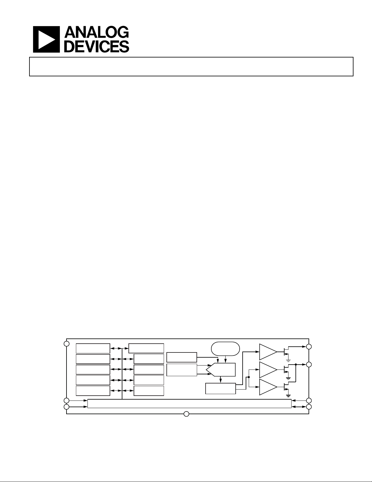
FUNCTIONAL BLOCK DIAGRAM
12
V
DD
A0
A1
Information furnished by Analog Devices is believed to be accurate and reliable. However, no
responsibility is assumed by Analog Devices for its use, nor for any infringements of patents or other
rights of third parties that may result from its use. Specifications subject to change without notice. No
license is granted by implication or otherwise under any patent or patent rights of Analog Devices.
Trademarks and registered trademarks are the property of their respective owners.
CONFIGURATION
RESET REGISTER
3
4
REGISTER
T
LOW
REGISTER
T
HYST
REGISTER
ID
REGISTER
SOFTWARE
TEMPERATURE
VALUE REGISTER
T
CRIT
REGISTER
T
HIGH
REGISTER
STATUS
REGISTER
POINTER
REGISTER
INTERNAL
REFERENCE
TEMPERATURE
SENSOR
ADT7420
I2C INTERFACE
11
GND
Figure 1.
I2C Temperature Sensor
GENERAL DESCRIPTION
The ADT7420 is a high accuracy digital temperature sensor
offering breakthrough performance over a wide industrial range,
housed in a 4 mm × 4 mm LFCSP package. It contains an internal
band gap reference, a temperature sensor, and a 16-bit ADC to
monitor and digitize the temperature to 0.0078°C resolution.
The ADC resolution, by default, is set to 13 bits (0.0625°C).
The ADC resolution is a user programmable mode that can be
changed through the serial interface.
The ADT7420 is guaranteed to operate over supply voltages from
2.7 V to 5.5 V. Operating at 3.3 V, the average supply current is typically 210 μA. The ADT7420 has a shutdown mode that powers
down the device and offers a shutdown current of typically 2.0 μA
at 3.3 V. The ADT7420 is rated for operation over the −40°C to
+150°C temperature range.
Pin A0 and Pin A1 are available for address selection, giving the
ADT7420 four possible I2C addresses. The CT pin is an open-
drain output that becomes active when the temperature exceeds
a programmable critical temperature limit. The INT pin is also
an open-drain output that becomes active when the temperature exceeds a programmable limit. The INT pin and CT pin
can operate in comparator and interrupt event modes.
PRODUCT HIGHLIGHTS
1. Ease of use, no calibration or correction required by the user.
2. Low power consumption.
3. Excellent long-term stability and reliability.
4. High accuracy for industrial, instrumentation, and medical
applications.
5. Packaged in a 16-lead, 4 mm × 4 mm LFCSP RoHScompliant package.
10
INTERNAL
OSCILLATOR
Σ-∆
MODULATOR
FILTER
LOGIC
One Technology Way, P.O. Box 9106, Norwood, MA 02062-9106, U.S.A.
Tel: 781.329.4700 www.analog.com
Fax: 781.461.3113 ©2011 Analog Devices, Inc. All rights reserved.
T
T
T
CRIT
HIGH
LOW
CT
9
INT
1
SCL
2
SDA
09013-001

ADT7420 Preliminary Technical Data
TABLE OF CONTENTS
Features .............................................................................................. 1
Applications ....................................................................................... 1
General Description ......................................................................... 1
Product Highlights ........................................................................... 1
Functional Block Diagram .............................................................. 1
Specifications ..................................................................................... 3
I2C Timing Specifications ............................................................ 5
Absolute Maximum Ratings ............................................................ 6
ESD Caution .................................................................................. 6
Pin Configuration and Function Descriptions ............................. 7
Typical Performance Characteristics ............................................. 8
Theory of Operation ...................................................................... 10
Circuit Information .................................................................... 10
Converter Details........................................................................ 10
Normal Mode .............................................................................. 10
One-Shot Mode .......................................................................... 10
1 SPS Mode .................................................................................. 11
Shutdown ..................................................................................... 11
Fault Queue ................................................................................. 11
Temperature Data Format ......................................................... 12
Temperature Conversion Formulas ......................................... 12
Registers ........................................................................................... 13
Address Pointer Register ........................................................... 13
Temperature Value Registers ..................................................... 13
Status Register ............................................................................. 14
Configuration Register .............................................................. 14
T
Setpoint Registers ............................................................. 15
HIGH
T
Setpoint Registers .............................................................. 15
LOW
T
Setpoint Registers .............................................................. 15
CRIT
T
Setpoint Register ............................................................... 16
HYST
ID Register................................................................................... 16
Serial Interface ................................................................................ 17
Serial Bus Address ...................................................................... 17
Writing Data ............................................................................... 18
Reading Data ............................................................................... 19
Reset ............................................................................................. 20
General Call ................................................................................ 20
INT and CT Outputs ...................................................................... 21
Undertemperature and Overtemperature Detection ............ 21
Applications Information .............................................................. 23
Thermal Response Time ........................................................... 23
Supply Decoupling ..................................................................... 23
Powering from a Switching Regulator ..................................... 23
Temperature Measurement ....................................................... 23
Quick Guide to Measuring Temperature ................................ 23
Outline Dimensions ....................................................................... 24
Ordering Guide .......................................................................... 24
Rev. PrE | Page 2 of 24

Preliminary Technical Data ADT7420
SPECIFICATIONS
TA = −40°C to +125°C, VDD = 2.7 V to 5.5 V, unless otherwise noted.
Table 1.
Parameter Min Typ Max Unit Test Conditions/Comments
TEMPERATURE SENSOR AND ADC
Accuracy
±0.25
±0.30 °C TA = −40°C to +105°C, VDD = 3.0 V
±0.35 °C TA = −40°C to +105°C, VDD = 2.7 V to 3.3 V
±0.50 °C TA = −40°C to +125°C, VDD = 3.0 V to 3.6 V
±0.503 °C TA = −10°C to +105°C, VDD = 4.5 V to 5.5 V
±0.65 °C TA = −40°C to +125°C, VDD = 4.5 V to 5.5 V
−0.85 °C TA = +150°C, VDD = 4.5 V to 5.5 V
−1.0 °C TA = +150°C, VDD = 2.7 V to 3.6 V
ADC Resolution 13 Bits Twos complement temperature value of the
16 Bits Twos complement temperature value of the
Temperature Resolution
Temperature Conversion Time 240 ms Continuous conversion and one-shot
Fast Temperature Conversion Time 6 ms First conversion on power-up only
1 SPS Conversion Time 60 ms Conversion time for 1 SPS mode
Temperature Hysteresis ±0.002 °C Temperature cycle = 25°C to 125°C and back
Repeatability
Drift5 0.0073 °C 500 hour stress test at +150°C with VDD = 5.0 V
DC PSRR 0.1 °C/V TA = 25°C
DIGITAL OUTPUTS (CT, INT, SDA—OPEN DRAIN)
High Output Leakage Current, IOH 0.1 5 µA CT and INT pins pulled up to 5.5 V
Output Low Voltage, V
Output High Voltage, VOH 0.7 × VDD V
Output Capacitance, C
DIGITAL INPUTS (SCL, SDA, A0, A1)
Input Current ±1 µA VIN = 0 V to VDD
Input Low Voltage, VIL 0.3 × VDD V SCL and SDA only
0.4 V A0 and A1 only
Input High Voltage, V
2 V A0 and A1 only
SCL, SDA Glitch Rejection 50 ns Input filtering suppresses noise spikes of less
Pin Capacitance 2 10 pF
POWER REQUIREMENTS
Supply Voltage 2.7 5.5 V
Supply Current
1
13-Bit 0.0625 °C 13-bit resolution (sign + 12-bit)
16-Bit 0.0078 °C 16-bit resolution (sign + 15-bit)
4
OL
OUT
IH
At 3.3 V 210 265 µA Peak current while converting, I2C interface
At 5.5 V 250 300 µA Peak current while converting, I2C interface
0.0017 ±0.20
±0.015 °C TA = 25°C
0.4 V IOL = 3 mA at 5.5 V, IOL = 1 mA at 3.3 V
2 pF
0.7 × VDD V SCL and SDA only
±0.25
2
°C TA = −10°C to +85°C, VDD = 3.0 V to 3.3 V
°C
°C
TA = −20°C to +105°C, VDD = 3.0 V to 3.6 V
TA = −20°C to +85°C, VDD = 2.7 V
sign bit plus 12 ADC bits (power-up default
resolution)
sign bit plus 15 ADC bits (Bit 7 = 1 in the
configuration register)
conversion modes
to 25°C
than 50 ns
inactive
inactive
Rev. PrE | Page 3 of 24

ADT7420 Preliminary Technical Data
Parameter Min Typ Max Unit Test Conditions/Comments
1 SPS Current
At 3.3 V 46 µA VDD = 3.3 V, 1 SPS mode, TA = 25°C
At 5.5 V 65 µA VDD = 5.5 V, 1 SPS mode, TA = 25°C
Shutdown Current
At 3.3 V 2.0 15 µA Supply current in shutdown mode
At 5.5 V 5.2 25 µA Supply current in shutdown mode
Power Dissipation Normal Mode 700 µW VDD = 3.3 V, normal mode at 25°C
Power Dissipation 1 SPS 150 µW Power dissipated for VDD = 3.3 V, TA = 25°C
1
Accuracy specification includes repeatability.
2
The equivalent 3 σ limits are ±0.15°C. This 3 σ specification is provided to enable comparison with other vendors who use these limits.
3
For higher accuracy at 5 V operation, contact Analog Devices, Inc.
4
Based on a floating average of 10 readings.
5
Drift includes solder heat resistance and life time test performed as per JEDEC Standard JESD22-A108.
Rev. PrE | Page 4 of 24
Preliminary Technical Data ADT7420
t
I2C TIMING SPECIFICATIONS
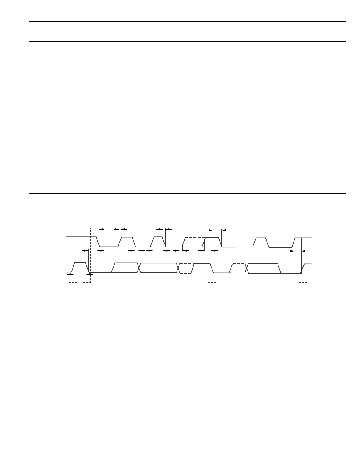
TA = −40°C to +150°C, VDD = 2.7 V to 5.5 V, unless otherwise noted. All input signals are specified with rise time (tR) = fall time (tF) = 5 ns
(10% to 90% of VDD) and timed from a voltage level of 1.6 V.
Table 2.
Parameter Min Typ Max Unit Test Conditions/Comments
SERIAL INTERFACE1 See Figure 2
SCL Frequency 0 400 kHz
SCL High Pulse Width, t
SCL Low Pulse Width, t
SCL, SDA Rise Time, tR 0.3 µs
SCL, SDA Fall Time, t
Hold Time (Start Condition), t
Setup Time (Start Condition), t
Data Setup Time, t
Setup Time (Stop Condition), t
Data Hold Time, t
HD:DAT
Bus-Free Time (Between Stop and Start Condition), t
Capacitive Load for Each Bus Line, CB
1
Sample tested during initial release to ensure compliance.
0.6 µs
HIGH
1.3 µs
LOW
F
0.6 µs After this period, the first clock is generated
HD:STA
0.6 µs Relevant for repeated start condition
SU:STA
0.02 µs
SU:DAT
0.6 µs
SU:STO
0.3 µs
(Master) 0.03 µs
1.3 µs
BUF
400 pF
Timing Diagram
SCL
SDA
t
BUF
P S
t
HD:STA
t
LOW
R
t
HD:DAT
t
F
t
HIGH
t
SU:DAT
t
SU:STA
S
Figure 2. Serial Interface Timing Diagram
t
HD:STA
t
SU:STO
P
09013-002
Rev. PrE | Page 5 of 24
ADT7420 Preliminary Technical Data
ABSOLUTE MAXIMUM RATINGS
Table 3.
Parameter Rating
VDD to GND −0.3 V to +7 V
SDA Voltage to GND −0.3 V to VDD + 0.3 V
SCL Output Voltage to GND −0.3 V to VDD + 0.3 V
A0 Input Voltage to GND −0.3 V to VDD + 0.3 V
A1 Input Voltage to GND −0.3 V to VDD + 0.3 V
CT and INT Output Voltage to GND −0.3 V to VDD + 0.3 V
ESD Rating (Human Body Model) 2.0 kV
Operating Temperature Range
1
−40°C to +150°C
Storage Temperature Range −65°C to +160°C
Maximum Junction Temperature, T
150°C
JMAX
16-Lead LFCSP (CP-16-17)
Power Dissipation2 W
MAX
= (T
JMAX
− T
3
A
Thermal Impedance4
θJA, Junction-to-Ambient (Still Air) 37°C/W
θJC, Junction-to-Case 33°C/W
IR Reflow Soldering 220°C
Peak Temperature (RoHS-Compliant
260°C (+0°C/−5°C)
Package)
Time at Peak Temperature 20 sec to 40 sec
Ramp-Up Rate 3°C/sec maximum
Ramp-Down Rate −6°C/sec maximum
Time from 25°C to Peak Temperature 8 minutes maximum
1
Sustained operation above 125°C results in a shorter product lifetime. For
more information, contact Analog Devices.
2
Values relate to package being used on a standard 2-layer PCB. This gives a
worst-case θJA and θJC.
3
TA = ambient temperature.
4
Junction-to-case resistance is applicable to components featuring a
preferential flow direction, for example, components mounted on a heat
sink. Junction-to-ambient is more useful for air-cooled, PCB-mounted
components.
)/θJA
Stresses above those listed under Absolute Maximum Ratings
may cause permanent damage to the device. This is a stress
rating only; functional operation of the device at these or any
other conditions above those indicated in the operational
section of this specification is not implied. Exposure to absolute
maximum rating conditions for extended periods may affect
device reliability.
ESD CAUTION
Rev. PrE | Page 6 of 24
Preliminary Technical Data ADT7420
NOTES
1. NC = NO CONNEC
BONDED
2.
EXPOSED
FLO
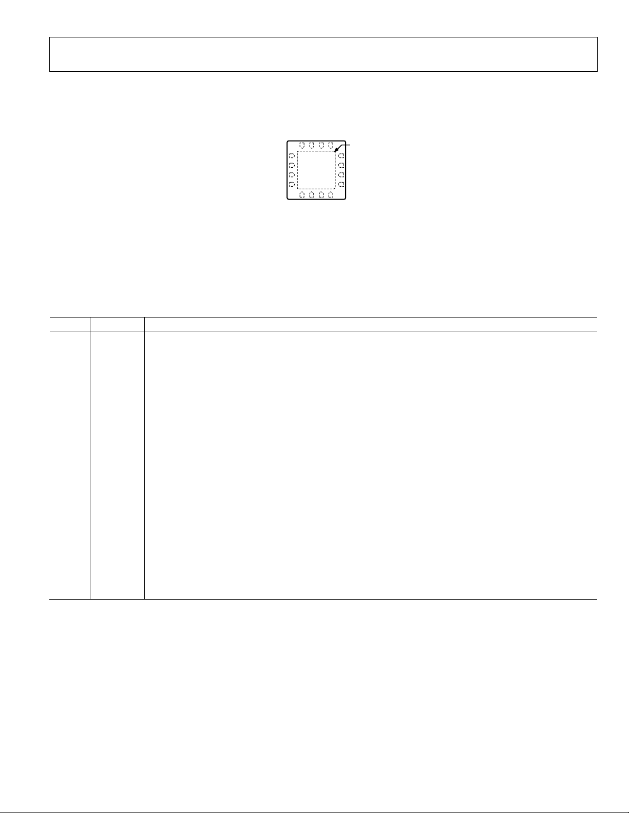
PIN CONFIGURATION AND FUNCTION DESCRIPTIONS
C
C
C
C
N
N
N
N
5
4
6
3
1
1
1
1
17 EP
1
SCL
SDA
A0
A1
TO ENSURE CORRECT OPERATION, THE
ADT7420
2
TOP VIEW
3
(Not to Scale)
4
5
6
C
C
N
N
T. THE NC PIN IS NOT
TO THE DIE INTERNALLY.
PAD SHOULD EITHER BE LEFT
ATING OR CONNECTED TO GROUND.
Figure 3. Pin Configuration
Table 4. Pin Function Descriptions
Pin No. Mnemonic Description
1 SCL I2C Serial Clock Input. The serial clock is used to clock in and clock out data to and from any register of the ADT7420.
Open-drain configuration. A pull-up resistor is required, typically 10 kΩ.
2 SDA I2C Serial Data Input/Output. Serial data to and from the part is provided on this pin. Open-drain configuration. A
pull-up resistor is required, typically 10 kΩ.
3 A0 I2C Serial Bus Address Selection Pin. Logic input. Connect to GND or VDD to set an I2C address.
4 A1 I2C Serial Bus Address Selection Pin. Logic input. Connect to GND or VDD to set an I2C address.
5 NC No Connect. The NC pin is not bonded to the die internally.
6 NC No Connect. The NC pin is not bonded to the die internally.
7 NC No Connect. The NC pin is not bonded to the die internally.
8 NC No Connect. The NC pin is not bonded to the die internally.
9 INT Overtemperature and Undertemperature Indicator. Logic output. Power-up default setting is as an active low
comparator interrupt. Open-drain configuration. A pull-up resistor is required, typically 10 kΩ.
10 CT Critical Overtemperature Indicator. Logic output. Power-up default polarity is active low. Open-drain configuration.
A pull-up resistor is required, typically 10 kΩ.
11 GND Analog and Digital Ground.
12 VDD Positive Supply Voltage (2.7 V to 5.5 V). The supply should be decoupled with a 0.1 µF ceramic capacitor to ground.
13 NC No Connect. The NC pin is not bonded to the die internally.
14 NC No Connect. The NC pin is not bonded to the die internally.
15 NC No Connect. The NC pin is not bonded to the die internally.
16 NC No Connect. The NC pin is not bonded to the die internally.
17 EP Exposed Pad. To ensure correct operation, the exposed pad should either be left floating or connected to ground.
12
V
DD
11
GND
10
CT
9
INT
8
7
C
C
N
N
09013-004
Rev. PrE | Page 7 of 24
ADT7420 Preliminary Technical Data
TEMPER
A
TURE ERROR (°C)
1.00
TEMPER
A
TURE ERROR (°C)
1.00
I
(
µ
A)
300
SHUTDOWN I
(
µ
A)
30
300
I
(
µ
A)
8
S
HU
T
D
O
W
N
I
(
µ
A
)
TYPICAL PERFORMANCE CHARACTERISTICS
0.75
0.50
0.25
–0.25
–0.50
–0.75
–1.00
0.75
0.50
0.25
–0.25
–0.50
–0.75
–1.00
0
–40–60 –20 0 20 40
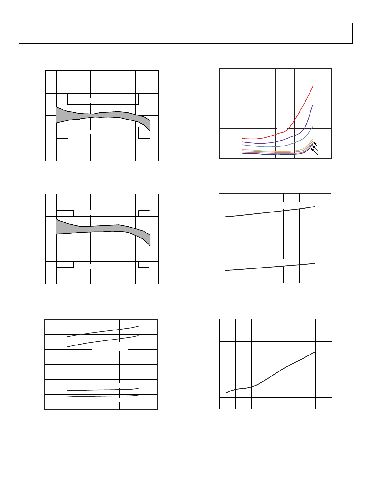
Figure 4. Temperature Accuracy at 3 V
0
–40–60 –20 0 20 40
Figure 5. Temperature Accuracy at 5 V
MAX ACCURACY LIMITS
MAX ACCURACY LIMITS
60 80 100 120 140
TEMPERATURE (°C)
MAX ACCURACY LIMITS
MAX ACCURACY LIMITS
60 80 100 120 140
TEMPERATURE (°C)
25
20
DD
15
10
5
0
–100 –50 0 50 100 150 200
09013-027
TEMPERATURE (°C)
5.5V
5.0V
4.5V
3.6V
3.3V
3.0V
2.7V
09013-032
Figure 7. Shutdown Current vs. Temperature
250
200
150
DD
100
50
0
2.5 3.0 3.5 4.0 4.5 5.0 5.5 6.0
09013-026
IDD CONTINUOUS CONVERSION
IDD 1SPS
SUPPLY VOLTAGE (V)
09013-029
Figure 8. Average Operating Supply Current vs. Supply Voltage
5.5V CONTINUOUS
250
200
150
DD
100
CONVERSION
3.0V CONTINUOUS
CONVERSION
5.5V 1SPS
50
0
–100 –50 0 50 100 150 200
3.0V 1SPS
TEMPERATURE (°C)
Figure 6. Operating Supply Current vs. Temperature
09013-028
7
6
5
DD
4
3
2
1
0
2.5 3.0 3.5 4.0 4.5 5.0 5.5 6.0
SUPPLY VOLTAGE (V)
Figure 9. Shutdown Current vs. Supply Voltage
09013-210
Rev. PrE | Page 8 of 24
 Loading...