

±2°C Accurate, 12-Bit Digital
A1A0A
V
www.BDTIC.com/ADI
FEATURES
12-bit temperature-to-digital converter
±2°C accuracy
Operation from −20°C to +125°C
Operation from 3 V to 3.6 V
240 μA typical average supply current
Selectable 1.5°C, 3°C, 6°C hysteresis
SMBus-/I2C®-compatible interface
Dual-purpose event pin: comparator or interrupt
8-lead LFCSP_VD, 3 mm × 3 mm (JEDEC MO-229 VEED-4)
package
Complies with JEDEC standard JC-42.4 memory module
Thermal sensor component specification
APPLICATIONS
Memory module temperature monitoring
Isolated sensors
Environmental control systems
Computer thermal monitoring
Thermal protection
Industrial process control
Power system monitors
1
2
2
3
Temperature Sensor
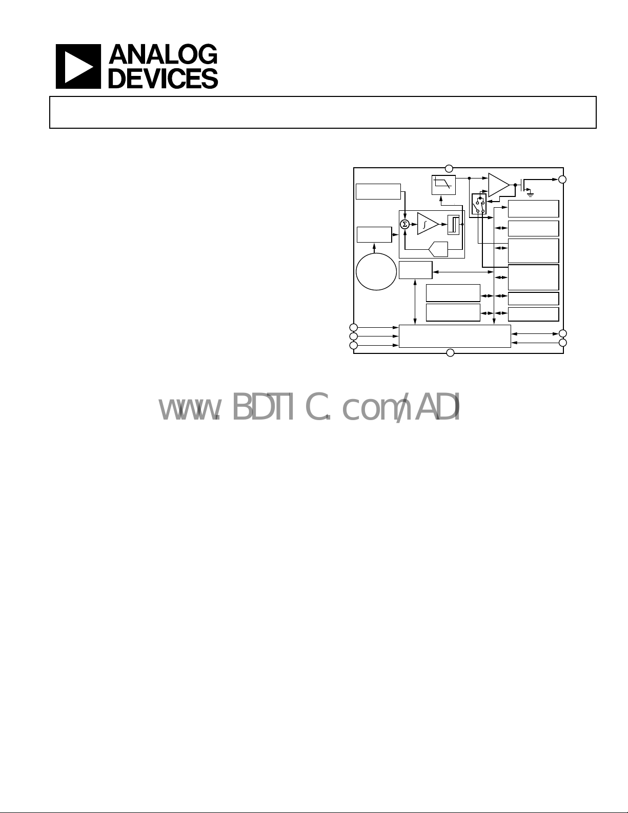
FUNCTIONAL BLOCK DIAGRAM
DD
8
12- / 10-Bit
LPF
B
I
T
-
1
1-BIT
DAC
MANUFACTURER’S
ID REGISTER
FACTORY
RESERVED
REGISTER
4
V
ss
Figure 1.
TEMPERATURE
SENSOR
REFERENCE
CLK
AND TIMING
GENERATION
ADT7408
DECIMATOR
+
–
∑-∆
ADDRESS
POINTER
REGISTER
SMBus/I²C I NTERFACE
ADT7408
DIGITAL CO MPARATOR
–
+
CAPABILITY
REGISTER
CONFIGURATIO N
REGISTER
ALARM TEMP
UPPER
BOUNDARY TRIP
REGISTER
ALARM TEMP
LOWER
BOUNDARY TRIP
REGISTER
CRITICAL TEMP
REGISTER
TEMPER ATURE
REGISTER
7
5
6
EVENT#
SDA
SCL
05716-001
GENERAL DESCRIPTION
The ADT7408 is the first digital temperature sensor that complies
with JEDEC standard JC-42.4 for the mobile platform memory
module. The ADT7408 contains a band gap temperature sensor
and a 12-bit ADC to monitor and digitize the temperature to a
resolution of 0.0625°C.
There is an open-drain EVENT# output that is active when the
onitoring temperature exceeds a critical programmable limit or
m
when the temperature falls above or below an alarm window.
This pin can operate in either comparator or interrupt mode.
There are three slave device address pins that allow up to eight
ADT7408s to be used in a system that monitors temperature of
various components and subsystems.
Rev. 0
Information furnished by Analog Devices is believed to be accurate and reliable. However, no
responsibility is assumed by Anal og Devices for its use, nor for any infringements of patents or ot her
rights of third parties that may result from its use. Specifications subject to change without notice. No
license is granted by implication or otherwise under any patent or patent rights of Analog Devices.
Trademarks and registered trademarks are the property of their respective owners.
The ADT7408 is specified for operation at supply voltages from
3.0 V t
o 3.6 V. Operating at 3.3 V, the average supply current is
less than 240 µA typical. The ADT7408 offers a shutdown mode
that powers down the device and gives a shutdown current of 3 μA
typical. The ADT7408 is rated for operation over the −20°C to
+125°C temperature range. The ADT7408 is available in a leadfree, 8-lead LFCSP_VD, 3 mm × 3 mm (JEDEC MO-229 VEED-4)
package.
One Technology Way, P.O. Box 9106, Norwood, MA 02062-9106, U.S.A.
Tel: 781.329.4700 www.analog.com
Fax: 781.461.3113 ©2006 Analog Devices, Inc. All rights reserved.

ADT7408
www.BDTIC.com/ADI
TABLE OF CONTENTS
Features.............................................................................................. 1
Applications....................................................................................... 1
Functional Block Diagram .............................................................. 1
General Description ......................................................................... 1
Revision History ............................................................................... 2
Specifications..................................................................................... 3
Timing Characteristics ................................................................ 4
Timing Diagram........................................................................... 4
Absolute Maximum Ratings............................................................ 5
ESD Caution.................................................................................. 5
Pin Configuration and Function Descriptions............................. 6
Typical Performance Characteristics ............................................. 7
Theory of Operation ........................................................................ 8
Circuit Information...................................................................... 8
Converter Details.......................................................................... 8
Address Pointer Register (Write Only).................................... 10
Capability Register (Read Only) .............................................. 10
Configuration Register (Read/Write)...................................... 11
Temperature Trip Point Registers ............................................ 13
ID Registers................................................................................. 14
Temperature Data Format......................................................... 15
Event Pin Functionality............................................................. 16
Serial Interface............................................................................ 17
SMBus/I
Application Information................................................................ 21
Thermal Response Time ........................................................... 21
Self-Heating Effects.................................................................... 21
Supply Decoupling..................................................................... 21
Temperature Monitoring........................................................... 21
Outline Dimensions....................................................................... 22
2
C Communications ................................................... 18
Modes of Operation ..................................................................... 8
Registers........................................................................................... 10
REVISION HISTORY
3/06—Revision 0: Initial Version
Ordering Guide .......................................................................... 22
Rev. 0 | Page 2 of 24
ADT7408
www.BDTIC.com/ADI
SPECIFICATIONS
All specifications TA = −20°C to +125°C, VDD = 3.0 V to 3.6 V, unless otherwise noted.
Table 1.
Parameter Symbol Min Typ Max Unit Test Conditions/Comments
TEMPERATURE SENSOR AND ADC
Local Sensor Accuracy (C Grade) ±0.5 ±2.0 °C
±1 ±3.0 °C
±1 ±4.0 °C
75°C ≤ T
40°C ≤ T
−20°C ≤ T
ADC Resolution 12 Bits
Temperature Resolution 0.0625 °C
Temperature Conversion Time 60 125 ms
Long Term Drift 0.081 °C Drift over 10 years, if part is operated at 55°C
EVENT# OUTPUT (OPEN DRAIN)
Output Low Voltage, VOL 0.4 V IOL = 3 mA
Pin Capacitance 10 pF
High Output Leakage Current IOH 0.1 1 µA EVENT# = 3.6 V
Rise Time
Fall Time1 t
1
tLH 30 ns
30 ns
HL
RON Resistance (Low Output)1 15 Ω Supply and temperature dependent
DIGITAL INPUTS
Input Current IIH, IIL −1 +1 µA VIN = 0 V to VDD
Input Low Voltage VIL 0.8 V
Input High Voltage VIH 2.1 V
3.0 V ≤
3.0 V ≤ V
SCL, SDA Glitch Rejection1 50 ns Input filtering suppresses noise spikes of less than 50 ns
Pin Capacitance1 10 pF
DIGITAL OUTPUT (OPEN DRAIN)
Output Low Current
Output Low Voltage VOL 0.4 V
IOL 6 mA SDA forced to 0.6 V
3.0 V ≤
Output High Voltage VOH 2.1 V
Output Capacitance
1
C
10 pF
OUT
POWER REQUIREMENTS
Supply Voltage VDD 3.0 3.3 3.6 V
Average Supply Current IDD 240 500 µA
Supply Current I
360 550 µA Device current while converting
DD_CONV
Shutdown Mode at 3.3 V 3 20 µA
Average Power Dissipation PD 790 µW VDD = 3.3 V, normal mode at 25°C
1
Guaranteed by design and characterization, not production tested.
≤ 95°C, 3.0 V ≤ VDD ≤ 3.6 V active range
A
≤ 125°C, 3.0 V ≤ VDD ≤ 3.6 V monitor range
A
≤ 125°C, 3.0 V ≤ VDD ≤ 3.6 V
A
≤ 3.6 V
V
DD
≤ 3.6 V
DD
V
DD
≤ 3.6 V at I
OPULL_UP
= 350 μA
Rev. 0 | Page 3 of 24
ADT7408
www.BDTIC.com/ADI
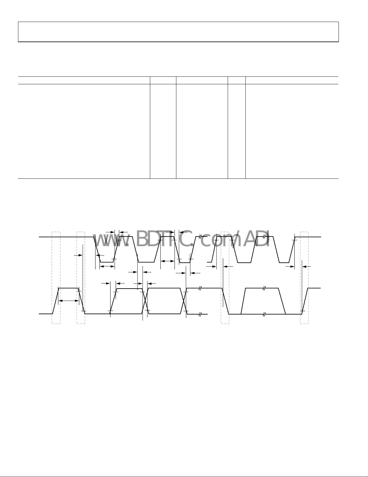
TIMING CHARACTERISTICS
TA = −20°C to +125°C, VDD = 3.0 V to 3.6 V, unless otherwise noted.
Table 2.
Parameter
SCL Clock Frequency f
Bus Free Time Between a Stop (P) and Start (S) Condition t
Hold Time After (Repeated) Start Condition t
Repeated Start Condition Setup Time t
High Period of the SCL Clock t
Low Period of the SCL Clock t
Fall Time of Both SDA and SCL Signals tF 300 ns
Rise Time of Both SDA and SCL Signals tR 1000 ns
Data Setup Time t
Data Hold Time t
Setup Time for Stop Condition t
Capacitive Load for Each Bus Line, C
1
Guaranteed by design and characterization, not production tested.
1
B
Symbol Min Typ Max Unit Comments
10 100 kHz
SCL
4.7 s
BUF
4.0 s
HD:STA
4.7 s
SU:STA
4.0 50 s
HIGH
4.7 s
LOW
250 ns
SU:DAT
300 ns
HD:DAT
4.0 s
SU:STO
After this period, the first clock
is genera
ted.
400 pF
TIMING DIAGRAM
V
IH
SCL
SDA
t
V
V
V
HD:STA
IL
IH
IL
t
BUF
PS P
t
LOW
t
R
t
HD:DAT
t
R
t
F
Figure 2. SMBus/I
t
F
t
HIGH
2
C Timing Diagram
t
SU:DAT
t
t
SU:STA
S
SU:STO
05716-002
Rev. 0 | Page 4 of 24
ADT7408
)
www.BDTIC.com/ADI
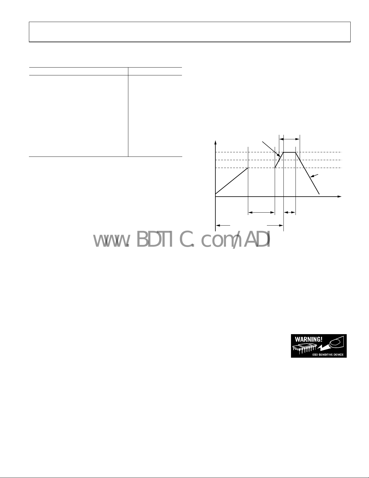
ABSOLUTE MAXIMUM RATINGS
Table 3.
Parameter Rating
VDD to VSS –0.3 V to +7 V
SDA Input Voltage to VSS –0.3 V to VDD + 0.3 V
SDA Output Voltage to VSS –0.3 V to VDD + 0.3 V
SCL Input Voltage to VSS –0.3 V to VDD + 0.3 V
EVENT# Output Voltage to VSS –0.3 V to VDD + 0.3 V
Operating Temperature Range –55°C to +150°C
Storage Temperature Range –65°C to +160°C
Maximum Junction Temperature, T
150°C
JMAX
Thermal Resistance1
θJA, Junction-to-Ambient (Still Air)
85oC/W
IR Reflow Soldering Profile Refer to Figure 3
1
Power Dissipation P
temperature. Thermal resistance value relates to the package being used on
a standard 2-layer PCB, which gives a worst-case θJA. Some documents may
publish junction-to-case thermal resistance θJC, but it refers to a component
that is mounted on an ideal heat sink. As a result, junction-to-ambient
thermal resistance is more practical for air-cooled, PCB-mounted
components.
MAX
= (T
− TA)/θJA, where TA is the ambient
JMAX
Stresses above those listed under Absolute Maximum Ratings
ma
y cause permanent damage to the device. This is a stress
rating only; functional operation of the device at these or any
other conditions above those indicated in the operational
section of this specification is not implied. Exposure to absolute
maximum rating conditions for extended periods may affect
device reliability.
RAMP UP
3°C/SE COND MAX
217°C
TEMPERATURE (° C)
60 – 150 SECONDS
260 – 5/+0°C
150°C – 200°C
RAMP DOW N
6°C/SECOND
MAX.
TIME (S econds
Figure 3.
60 – 180 SECONDS 20 – 40 SECONDS
480 SECONDS MAX.
LFCSP Pb-Free Reflow Profile Based on JEDEC J-STD-20C
ESD CAUTION
ESD (electrostatic discharge) sensitive device. Electrostatic charges as high as 4000 V readily accumulate on
the human body and test equipment and can discharge without detection. Although this product features
proprietary ESD protection circuitry, permanent damage may occur on devices subjected to high energy
electrostatic discharges. Therefore, proper ESD precautions are recommended to avoid performance degradation or loss of functionality.
05716-003
Rev. 0 | Page 5 of 24

ADT7408
V
www.BDTIC.com/ADI
PIN CONFIGURATION AND FUNCTION DESCRIPTIONS
A0 1
ADT7408
A1 2
TOP VIEW
A2 3
(Not to scal e)
4
SS
Figure 4. Pin Configuration
8 V
DD
7 EVENT#
6 SCL
5 SDA
05716-004
Table 4. Pin Function Descriptions
Pin No. Mnemonic Description
1 A0 SMBus/I2C Serial Bus Address Selection Pin. Logic input. Can be set to VSS or VDD.
2 A1 SMBus/I2C Serial Bus Address Selection Pin. Logic input. Can be set to VSS or VDD.
3 A2 SMBus/I2C Serial Bus Address Selection Pin. Logic input. Can be set to VSS or VDD.
4 V
5 SDA
Negative Supply or Ground.
SS
SMBus/I
2
C Serial Data Input/Output. Serial data to be loaded into the part’s registers and read from these registers
is provided on this pin. Open-drain configuration; it needs a pull-up resistor.
6 SCL
Serial Clock Input. This is the clock input f
or the serial port. The serial clock is used to clock data into and clock data
out from any register of the ADT7408. Open-drain configuration needs a pull-up resistor.
7 EVENT# Active Low. Open-drain event output pin. Driven low on comparator level or alert interrupt.
8 VDD Positive Supply Power. The supply should be decoupled to ground.
Rev. 0 | Page 6 of 24
ADT7408
www.BDTIC.com/ADI
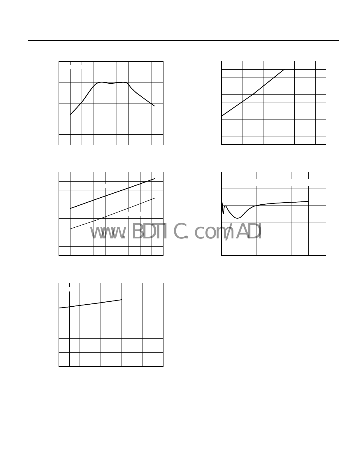
TYPICAL PERFORMANCE CHARACTERISTICS
0.4
VDD = 3.3V
0.3
0.2
0.1
0
–0.1
–0.2
TEMPERATURE E RROR (° C)
–0.3
–0.4
–40 20 400–20 60 80 100 120 140
TEMPERATURE (° C)
Figure 5. Temperature Accuracy
05716-015
5.0
TA = 85°C
4.5
4.0
3.5
3.0
2.5
2.0
1.5
SHUTDOWN CURRENT (µA)
1.0
0.5
0
3.0 3. 1 3.2 3.3 3.4 3.5 3.6 3.7 3.8 3.9 4.0
SUPPLY VOLTAGE (V)
Figure 8. Shutdown Current vs. Supply Voltage
05716-016
450
400
350
300
250
200
150
100
AVERAGE SUPPLY CURRENT (µA)
50
0
–40 –20 0 20 40 60 80 100 120 140
CONVERTING 3.3V
AVERAGE 3.3V
TEMPERATURE ( °C)
Figure 6. Supply Current vs. Temperature
300
TA = 85°C
275
250
225
200
0.25
TA = 85°C
V
= 3.3V ± 10%
DD
A 0.1µF CAPACIT OR IS CO NNECTED AT THE V
0.20
0.15
0.10
TEMPERATURE E RROR (° C)
0.05
05716-017
0
0123 54
SUPPLY RIPPLE FREQUENCY (MHz)
PIN.
DD
05716-018
6
Figure 9. Temperature Accuracy vs. Supply Ripple Frequency
175
AVERAGE SUPPLY CURRENT (µA)
150
3.0 3. 1 3.2 3.3 3.4 3.5 3.6 3.7 3.8 3.9 4.0
SUPPLY VOLTAGE (V)
05716-019
Figure 7. Supply Current vs. Supply Voltage
Rev. 0 | Page 7 of 24
ADT7408
www.BDTIC.com/ADI
THEORY OF OPERATION
CIRCUIT INFORMATION
The ADT7408 is a 12-bit digital temperature sensor presented
in 13 bits, including the sign bit format (see the bit map in the
Temperature Value Register (Read Only) section). Its output is
os complement in that Bit D12 is the sign bit and Bit D0 to
tw
Bit D11 are data bits. An on-board sensor generates a voltage
precisely proportional to absolute temperature, which is
compared to an internal voltage reference and input to a
precision digital modulator. Overall accuracy for the ADT7408
is ±2°C from 75°C to 95°C, ±3°C from 40°C to +125°C, and
±4°C from −20°C to +125°C, with excellent transducer linearity.
The serial interface is SMBus-/I
2
C-compatible, and the open-
drain output of the ADT7408 is capable of sinking 6 mA.
The on-board temperature sensor has excellent accuracy and
arity over the entire rated temperature range without
line
needing correction or calibration by the user.
A first-order ∑-∆ modulator, also known as the charge balance
t
ype analog-to-digital converter (ADC), digitizes the sensor
output. This type of converter utilizes time domain oversampling
and a high accuracy comparator to deliver 12 bits of effective
accuracy in an extremely compact circuit.
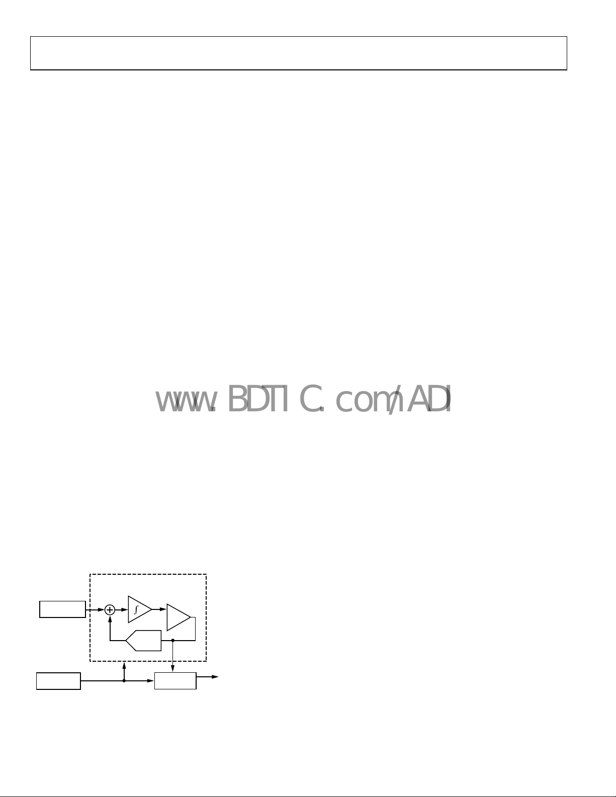
CONVERTER DETAILS
The ∑-∆ modulator consists of an input sampler, a summing
network, an integrator, a comparator, and a 1-bit DAC, as
shown in Figure 10. This architecture creates a negative
feedback loop that minimizes the integrator output by changing
the duty cycle of the comparator output in response to input
voltage changes. There are two simultaneous but different
sampling operations in the device. The comparator samples the
output of the integrator at a much higher rate than the input
sampling frequency, that is, oversampling. Oversampling
spreads the quantization noise over a much wider band than
that of the input signal, improving overall noise performance
and increasing accuracy.
The modulated output of the comparator is encoded using a
cir
cuit technique that results in SMBus/I
Σ-∆ MODULATOR
VOLTAGE REF
AND VPTAT
CLOCK
GENERATOR
INTEGRATOR
+
–
Figure 10. First-Order Σ-Δ Modulator
1-BIT
DAC
LPF DIGITAL
COMPARATOR
2
C temperature data.
+
–
1-BIT
FILTER
12-BIT
TEMPERATURE
VALUE REGISTER
5716-005
MODES OF OPERATION
The conversion clock for the part is internally generated. No
external clock is required except when reading from and writing
to the serial port. In normal mode, the internal clock oscillator
runs an automatic conversion sequence that initiates a
conversion every 100 ms. At this time, the part powers up its
analog circuitry and performs a temperature conversion. This
temperature conversion typically takes 60 ms, after which time
the analog circuitry of the part automatically shuts down. The
analog circuitry powers up again 40 ms later, when the 100 ms
timer times out and the next conversion begins. Because the
SMBus/I
recent temperature conversion is always available in the
temperature value register.
The ADT7408 can be placed in shutdown mode via the
co
shut down, and no further conversions are initiated until the
ADT7408 is taken out of shutdown mode by writing 0 to Bit D8
in the configuration register. The conversion result from the last
conversion prior to shutdown can still be read from the ADT7408,
even when it is in shutdown mode.
In normal conversion mode, the internal clock oscillator is reset
a
start a temperature conversion, the result of which is typically
available 60 ms later. Similarly, when the part is taken out of
shutdown mode, the internal clock oscillator starts, and a
conversion is initiated. The conversion result is typically available
60 ms later. Reading from the device before a conversion is complete does not stop the ADT7408 from converting; the part does
not update the temperature value register immediately after the
conversion but waits until communication to the part is finished.
This read operation provides the previous result. It is possible to
miss a conversion result if the SCL frequency is very slow
(communication is greater than 40 ms), because the next
conversion will have started. There is a 40 ms window between
the end of one conversion and the start of the next conversion
for the temperature value register to be updated with a new
temperature value.
The measured temperature value is compared with the
t
emperature set at the alarm temperature upper boundary trip
register, the alarm temperature lower boundary trip register,
and the critical temperature trip register. If the measured value
exceeds these limits, then the EVENT# pin is activated. This
EVENT# output is programmable for interrupt mode, comparator
mode, and the output polarity via the configuration register.
The thermal sensor continuously monitors the temperature and
u
data is latched internally by the device and can be read by
software from the bus host at any time.
2
C circuitry never shuts down, the result of the most
nfiguration register, in which case the on-chip oscillator is
fter every read or write operation. This causes the device to
pdates the temperature data 10 times per second. Temperature
Rev. 0 | Page 8 of 24

ADT7408
www.BDTIC.com/ADI
SMBus/I2C slave address selection pins allow up to eight such
devices to co-exist on the same bus. This means that up to eight
memory modules can be supported, given that each module has
one slave device address slot.
After initial power-on, the configuration registers are set to the
defa
ult values. Software can write to the configuration register
to set bits as per the bit definitions in the Registers section.
Rev. 0 | Page 9 of 24

ADT7408
www.BDTIC.com/ADI
REGISTERS
The ADT7408 contains 16 accessible registers, shown in Table 5 .
The address pointer register is the only register that is eight bits;
the other registers are 16 bits wide. On power-up, the address
pointer register is loaded with 0x00 and points to the capability
register.
Table 5. Registers
Pointer
Address Name
Not
Applicable
0x00 Capability Register 0x001D Read
0x01 Configuration Register 0x0000 Read/Write
0x02
0x03
0x04
0x05
0x06
0x07
0x08 to 0x0F
Address Pointer
Register
Alarm Temperature
Upper Boundar
Trip Register
Alarm Temperature
r Boundary
Lowe
Trip Register
Critical Temperature
ip Register
Tr
Temperature Value
gister
Re
Manufacturer ID
gister
Re
Device ID/Revision
gister
Re
Vendor-Defined
egisters
R
Power-On
Default Read/Write
0x00 Write
0x0000 Read/Write
y
0x0000 Read/Write
0x0000 Read/Write
Undefined Read
0x11D4 Read
0x080X Read
0x0000 Reserved
MSB LSB
D15 D14 D13 D12 D11 D10 D9 D8 D7 D6 D5 D4 D3 D2 D1 D0
RFU RFU RFU RFU RFU RFU RFU RFU RFU RFU RFU TRES1 TRES0
Table 7. Capability Mode Description
Bit Function
D0
Alarm/Critical Trips
D1
Higher Precision
D2
Wider Range
[D4:D3]
Temperature Resolution
[D15:D5] Reserved for future use; must be 0
Basic capability
D0 Trips Capability
1 Alarm and critical trips capability
Accuracy
D1 Accuracy Capability
0 Default accuracy ±2°C over the active range and ±3°C over the monitor range
Wider range
D2 Temperature Range Capability
1 Can read temperature below 0°C and set sig
Temperature resolution
[D4:D3] Temperature Resolution
01 0.25°C LSB
11 0.0625°C LSB (default)
ADDRESS POINTER REGISTER (WRITE ONLY)
This 8-bit write only register selects which of the 16-bit registers
is accessed in subsequent read/write operations. Address space
between 0x08 and 0x0F is reserved for factory usage.
MSB LSB
D7 D6 D5 D4 D3 D2 D1 D0
0 0 0 0
Register
selec
t
Register
select
Register
select
Register
select
Table 6. Address Pointer Selected Registers
D2 D1 D0 Register Selected
0 0 0 Capability Register
0 0 1 Configuration Register
0 1 0
0 1 1
1 0 0 Critical Temperature Trip Register
1 0 1 Temperature Value Register
1 1 0 Manufacturer ID Register
1 1 1 Device ID/Revision Register
Alarm Temperature Upper Boundary Trip
gister
Re
Alarm Temperature Lower Boundary Trip
gister
Re
CAPABILITY REGISTER (READ ONLY)
This 16-bit, read-only register indicates the capabilities of the
thermal sensor, as shown in Ta bl e 7 and the following bit map.
N
ote that RFU means reserved for future use.
Wider
ge
ran
n bit accordingly (default)
Higher
precision
Alarm/Critical
trips
Rev. 0 | Page 10 of 24

ADT7408
www.BDTIC.com/ADI
CONFIGURATION REGISTER (READ/WRITE)
This 16-bit read/write register stores various configuration modes for the ADT7408, as shown in Tabl e 8 and the following bit map.
Note that RFU means reserved for future use.
MSB LSB
D15 D14 D13 D12 D11 D10 D9 D8 D7 D6 D5 D4 D3 D2 D1 D0
RFU RFU RFU RFU RFU Hysteresis
Shutdo
mode
Table 8. Configuration Mode Description
Bit Description
D0 Event mode
0: Comparator output mode (default)
1: Interrupt mode
When either lock bit (D6 and D7) is set, this bit cannot be altered until unlocked.
D1 Event polarity
0: Active low (default)
1: Active high
When either lock bit (D6 and D7) is set, this bit cannot be altered until unlocked.
D2 Critical event only
0: Event output on alarm or critical temperature event (default)
1: Event only if temperature is above the value in the critical temperature trip register
When either lock bit (D6 and D7) is set, this bit cannot be altered until unlocked.
D3 Event output control
0: Event output disabled (default)
1: Event output enabled
When either lock bit (D6 and D7) is set, this bit cannot be altered until unlocked.
D4 Event output status (read only)
0: Event output condition is not being asserted by this device
1: Event output pin is being asserted by this device due to alarm window or critical trip condition
D5 Clear event (write only)
0: No effect
1: Clears an active event in interrupt mode
D6 Alarm window lock bit
0: Alarm trips are not locked and can be altered (default)
1: Alarm trip register settings cannot be altered
D7 Critical trip lock bit
0: Critical trip is not locked and can be altered (default)
1: Critical trip register settings cannot be altered
D8 Shutdown mode
0: TS enabled (default)
1: TS shut down
The actual cause of an event can be determined from the read of the temper
by writing to the clear event bit. Writing to this bit has no effect on the output status because it is a read function only.
Writing to this register has no effect in comparator mode. When
is greater than the critical temperature, an event cannot be cleared (see Figure 12).
This bit is initially cleared. When set, this bit r
can be written with a single write and do not require double writes.
This bit is initially cleared. When set, this bit r
can be written with a single write and do not require double writes.
When shut down, the thermal sensing device and ADC are disabled to sa
is set, this bit cannot be set until unlocked. However, it can be cleared at any time.
Critical
wn
lock bit
eturns a 1 and remains locked until cleared by internal power on reset. These bits
eturns a 1 and remains locked until cleared by internal power on reset. These bits
Alarm
lock bit
read, this bit always returns 0. Once the DUT temperature
Rev. 0 | Page 11 of 24
Clear
event
Event
output
status
ature value register. Interrupt events can be cleared
ve power. No events are generated. When either lock bit
Event
output
control
Critical
event
only
Event
polarity
Event
mode

ADT7408
www.BDTIC.com/ADI
Bit Description
D10:D9 Hysteresis enable
00: Disable hysteresis
01: Enable hysteresis at 1.5°C
10: Enable hysteresis at 3°C
11: Enable hysteresis at 6°C
T
H
T
L
T
H – HYST
T
L – HYST
BELOW WINDOW BIT
ABOVE WINDO W BIT
Figure 11. Hysteresis
05716-006
Rev. 0 | Page 12 of 24

ADT7408
www.BDTIC.com/ADI
TEMPERATURE TRIP POINT REGISTERS
There are three temperature trip point registers. They are the alarm temperature upper boundary trip register, the alarm temperature
lower boundary trip register, and the critical temperature trip register.
Alarm Temperature Upper Boundary Trip Register (Read/Write)
The value is the upper threshold temperature value for alarm mode. The data format is twos complement with one LSB = 0.25oC.
RFU (reserved for future use) bits are not supported and always report 0. Interrupts respond to the programmed boundary values.
If boundary values are being altered in-system, the user should turn off interrupts until a known state can be obtained to avoid
superfluous interrupt activity. The format of this register is shown in the following bit map:
Sign
MSB
D15 D14 D13 D12 D11 D10 D9 D8 D7 D6 D5 D4 D3 D2 D1 D0
0 0 0 Alarm window upper boundary temperature RFU RFU
Alarm Temperature Lower Boundary Trip Register (Read/Write)
The value is the lower threshold temperature value for alarm mode. The data format is twos complement with one LSB = 0.25oC.
RFU bits are not supported and always report 0. Interrupts respond to the programmed boundary values. If boundary values are being
altered in-system, the user should turn off interrupts until a known state can be obtained to avoid superfluous interrupt activity. The
format of this register is shown in the following bit map:
D15 D14 D13 D12 D11 D10 D9 D8 D7 D6 D5 D4 D3 D2 D1 D0
0 0 0 Alarm window upper boundary temperature RFU RFU
Sign
MSB
Critical Temperature Trip Register (Read/Write)
The value is the critical temperature. The data format is twos complement with one LSB = 0.25oC. RFU bits are not supported and always
report 0. The format of this register is shown in the following bit map:
D15 D14 D13 D12 D11 D10 D9 D8 D7 D6 D5 D4 D3 D2 D1 D0
0 0 0 Critical temperature trip point RFU RFU
Sign
MSB
Temperature Value Register (Read Only)
This 16-bit, read-only register stores the trip status and the temperature measured by the internal temperature sensor, as shown in Tab l e 9 .
The temperature is stored in 13-bit, twos complement format with the MSB being the temperature sign bit and the 12 LSBs representing
temperature. One LSB = 0.0625
o
C. The most significant bit has a resolution of 128oC.
LSB
LSB
LSB
When reading from this register, the eight MSBs (Bit D15 to Bit D8) are read first, and then the eight LSBs (Bit D7 to Bit D0) are
The trip status bits represent the internal temperature trip detection and are not affected by the status of the event or configura
for example, event output control, clear event. If both above and below are 0, then the current temperature is exactly within the alarm
window boundaries, as defined in the configuration register. The format and descriptions are shown in
D15 D14 D13 D12 D11 D10 D9 D8 D7 D6 D5 D4 D3 D2 D1 D0
Above
critical
trip
Above
alarm
window
Below
alarm
window Temperature
Sign
MSB
Rev. 0 | Page 13 of 24
read.
tion bits,
Tabl e 9 and the following bit map:
LSB

ADT7408
www.BDTIC.com/ADI
Table 9. Temperature Register Trip Status Description
Bit Definition
D13
Below alarm window
D14
Above alarm window
D15
Above critical trip
ID REGISTERS
Manufacturer ID Register (Read Only)
This manufacturer ID matches that assigned to a vendor within the PCI SIG. This register can be used to identify the manufacturer of the
device in order to perform manufacturer-specific operations. Manufacturer IDs can be found at www.pcisig.com. The format of this
egister is shown in the following bit map:
r
D15 D14 D13 D12 D11 D10 D9 D8 D7 D16 D5 D4 D3 D2 D1 D0
0 0 0 1 0 0 0 1 1 1 0 1 0 1 0 0
Device ID and Revision Register (Read Only)
This device ID and device revision are assigned by the device manufacturer. The device revision starts at 0 and is incremented by 1
whenever an update to the device is issued by the manufacturer. The format of this register in shown in the following bit map:
D15 D14 D13 D12 D11 D10 D9 D8 D7 D6 D5 D4 D3 D2 D1 D0
0 0 0 0 1 0 0 0 0 0 0 0 0 0 0 1
Below alarm window
D13 Temperature Alarm Status
0 Temperature is equal to or above the alarm window lower boundary temperature.
1 Temperature is below the alarm window lower boundary temperature.
Above alarm window
D14 Temperature Alarm Status
0 Temperature is equal to or below the alarm window upper boundary temperature.
1 Temperature is above the alarm window upper boundary temperature.
Above critical trip
D15 Critical Trip Status
0 Temperature is below the critical temperature setting.
1 Temperature is equal to or above the critical temperature setting.
Rev. 0 | Page 14 of 24

ADT7408
www.BDTIC.com/ADI
TEMPERATURE DATA FORMAT
The values used in the temperature register and three
temperature trip point registers are in twos complement format.
The temperature register has a 12-bit resolution with 256°C
range with 1 LSB = 0.0625°C (256°C/2
temperature data in the three temperature trip point registers
(alarm upper, alarm lower, and critical) is a 10-bit format with
256°C range with 1 LSB = 0.25°C (see the bit maps in the
emperature Lower Boundary Trip Register (Read/Write)
T
secti
on, the Critical Temperature Trip Register (Read/Write)
s
ection, and the Temperature Value Register (Read Only) section.)
Bi
t D12 in all these registers represents the sign bit such that
0 = positive temperature and 1 = negative temperature. In twos
complement format, the data bits are inverted and add 1 if
Bit D12 (the sign bit) is negative.
Temperature Conversion Formulas
12-Bit Temperature Data Format
Positive Temperature = ADC Code(d)/16 (1)
Negative Temperature = (ADC Code(d) − 4096)/16
where d is t
he 12-bit digital output in decimal.
Note that Bit D12 (the sign bit) is not included in the ADC
de, but the sign is inserted in the final result.
co
Tabl e 1 0 tabulates some temperature results vs. digital outputs.
10-Bit Temperature Data Format
Positive Temperature = ADC Code(d)/4 (3)
Negative Temperature = (ADC Code(d) − 1024)/4
12
); see Table 10. The
Alarm
(2)
(4)
Similarly, Bit D12 (the sign bit) is not included in the ADC
de, but the sign is inserted in the final result. This ADC code
co
contains DB2 to DB11. DB0 to DB1 are not in this calculation.
Although one LSB of the ADC corresponds to 0.0625°C, the
C can theoretically measure a temperature range of 255°C
AD
(−128°C to +127°C ). The ADT7408 is guaranteed to measure
a low value temperature limit of −55°C to a high value temperature
limit of +125°C.
Reading back the temperature from the temperature value
register requires a 2-byte read
.
Designers accustomed to using a 9-bit temperature data format
can still use
the ADT7408 by ignoring the last three LSBs of the
12-bit temperature value.
Table 10. 12-Bit Temperature Data Format
Digital Output (Binary)
D12 to D0
1 1100 1001 0000 C90 −55°C
1 1100 1110 0000 CE0 −50°C
1 1110 0110 1111 E6F −25°C
1 1111 1111 1111 FFF −0.0625°C
0 0000 0000 0000 000 0°C
0 0000 0000 0001 0x001 +0.0625°C
0 0000 1010 0000 0x0A0 +10°C
0 0001 1001 0000 0x190 +25°C
0 0011 0010 0000 0x320 +50°C
0 0100 1011 0000 0x4B0 +75°C
0 0110 0100 0000 0x640 +100°C
0 0111 1101 0000 0x7D0 +125°C
Digital Output
x)
(He
Temperature
Rev. 0 | Page 15 of 24

ADT7408
www.BDTIC.com/ADI
EVENT PIN FUNCTIONALITY
Figure 12 shows the three differently defined outputs of EVENT#
corresponding to the temperature change. EVENT# can be
programmed to be one of the three output modes in the
configuration register.
If while in interrupt mode the temperature reaches the critical
t
emperature, the device switches to the comparator mode
automatically and asserts the EVENT# output. When the
temperature drops below the critical temperature, the part
switches back to either interrupt mode or comparator mode,
as programmed in the configuration register.
Note that Figure 12 is drawn with no hysteresis, but the values
p
rogrammed into Configuration Register 0x01, Bit[10:9] affect
the operation of the event trigger points. See Figure 11 for the
e
xplanation of hysteresis functionality.
Event Thresholds
All event thresholds use hysteresis as programmed in the
Configuration Register 0x01, Bit[10:9] to set when they
deassert.
Critical Trip
The device can be programmed in such a way that the EVENT#
output is triggered only when the temperature exceeds critical
trip point. The critical temperature setting is programmed in
the critical temperature register. When the temperature sensor
reaches the critical temperature value in this register, the device
is automatically placed in comparator mode, meaning that the
critical event output cannot be cleared through software by
setting the clear event bit.
Interrupt Mode
After an event occurs, software can write a 1 to the clear event
bit in the configuration register to de-assert the EVENT#
interrupt output, until the next trigger condition occurs.
Comparator Mode
Reads/writes on the device registers do not affect the EVENT#
output in comparator mode. The EVENT# signal remains
asserted until the temperature drops outside the range or until
the range is reprogrammed such that the current temperature is
outside the range.
Alarm Window Trip
The device provides a comparison window with an upper
temperature trip point in the alarm upper boundary register
and a lower trip point in the alarm lower boundary register.
When enabled, the EVENT# output is triggered whenever entering
or exiting (crossing above or below) the alarm window.
TEMPERATURE
CRITICAL
ALARM
WINDOW
S/W CLEARS EVENT
EVENT# IN “I NTERRUPT”
EVENT# IN “CO MPARATOR” M ODE
HYSTERESIS AFFECTS
THESE TRIP POINTS
TIME
EVENT# IN “CRI TICAL T EMP ONLY” MODE
1. EVENT# CANNOT BE CLEARED ONCE THE DUT TEM PERATURE
IS GREATER THAN THE CRITICAL TEMPE RATURE
Figure 12. Temperature, Trip, and Events
Rev. 0 | Page 16 of 24
05716-007

ADT7408
www.BDTIC.com/ADI
SERIAL INTERFACE
Control of the ADT7408 is carried out via the SMBus-/I2Ccompatible serial interface. The ADT7408 is connected to this
bus as a slave and is under the control of a master device.
2
Figure 13 shows a typical SMBus/I
PULLUP
V
DD
10kΩ
ADT7408
EVENT#
A0
A1
A2
Figure 13. Typical SMBus/I
SCL
SDA
GND
Serial Bus Address
Like all SMBus-/I2C-compatible devices, the ADT7408 has a 7-bit
serial address. The four MSBs of this address for the ADT7408 are
set to 0011. The three LSBs are set by Pin 1, Pin 2, and Pin 3
(A0, A1, and A2). These pins can be configured either low or
high, permanently or dynamically, to give eight different
address options.
opt
ions available. Recommended pull-up resistor value on the
Tabl e 1 1 shows the different bus address
SDA and SCL lines is 2.2 kΩ to 10 kΩ .
2
Table 11. SMBus/I
C Bus Address Options
BINARY
A6 to A0
0011 0 0 0 0x18
0011 0 0 1 0x19
0011 0 1 0 0x1A
0011 0 1 1 0x1B
0011 1 0 0 0x1C
0011 1 0 1 0x1D
0011 1 1 0 0x1E
0011 1 1 1 0x1F
The ADT7408 has been designed with a SMBus/I2C timeout.
2
The SMBus/I
C interface times out after 75 ms to 100 ms of no
activity on the SDA line. After this timeout the ADT7408 resets
the SDA line back to its idle state (SDA set to high impedance)
and waits for the next start condition.
C interface connection.
PULLUP
V
2
C Interface Connection
V
10kΩ
DD
10kΩ
DD
HEX
05716-008
The serial bus protocol operates as follows:
1. The mast
er initiates data transfer by establishing a start
condition, defined as a high-to-low transition on the serial
data line SDA, while the serial clock line, SCL, remains
high. This indicates that an address/data stream follows.
All slave peripherals connected to the serial bus respond to
the start condition and shift in the next eight bits,
consisting of a 7-bit address (MSB first) plus a R/
W
The R/
bit determines whether data is written to, or read
W
bit.
from, the slave device.
2. The p
eripheral with the address corresponding to the
transmitted address responds by pulling the data line low
during the low period before the ninth clock pulse, known
as the acknowledge bit. All other devices on the bus now
remain idle while the selected device waits for data to be
read from or written to it. If the R/
master writes to the slave device. If the R/
W
bit is a 0, then the
W
bit is a 1, the
master reads from the slave device.
ta is sent over the serial bus in sequences of nine clock
3. Da
pulses: eight bits of data followed by an acknowledge bit
from the receiver of data. Transitions on the data line must
occur during the low period of the clock signal and remain
stable during the high period, because a low to high
transition when the clock is high can be interpreted as a
stop signal.
4. Whe
n all data bytes have been read or written, stop
conditions are established. In write mode, the master pulls
the data line high during the 10th clock pulse to assert a
stop condition. In read mode, the master device pulls the
data line high during the low period before the ninth clock
pulse. This is known as no acknowledge. The master then
takes the data line low during the low period before the
10th clock pulse, then high during the 10th clock pulse to
assert a stop condition.
Any number of bytes of data can be transferred over the serial
us in one operation. However, it is not possible to mix read
b
and write in one operation because the type of operation is
determined at the beginning and cannot subsequently be
changed without starting a new operation.
2
C address set up by the three address pins is not latched
The I
by the device until after this address has been sent twice. On the
eighth SCL cycle of the second valid communication, the serial
bus address is latched in. This is the SCL cycle directly after the
device has seen its own I
changes on this pin have no effect on the I
2
C serial bus address. Any subsequent
2
C serial bus address.
Rev. 0 | Page 17 of 24

ADT7408
www.BDTIC.com/ADI
SMBUS/I2C COMMUNICATIONS
The data registers in the ADT7408 are selected by the pointer
register. At power-up the pointer register is set to 0x00, the
location for the capability register. The pointer register latches
the last location to which it was set. Each data register falls into
one of the following three types of user accessibility:
• Re
ad only
• Wr
• W
A write to the ADT7408 always includes the address byte and
he pointer byte. A write to any register other than the pointer
t
register requires two data bytes.
Reading data from the ADT7408 occurs in one of the following
o ways:
tw
• I
ite o n ly
rite/Read same address
f the location latched in the pointer register is correct,
then the read simply consists of an address byte,
followed by retrieving the two data bytes.
The data byte has the most significant bit first. At the end of a
ead, the ADT7408 accepts either acknowledge (ACK) or no
r
acknowledge (NO ACK) from the master. No acknowledge is
typically used as a signal for the slave that the master has read
its last byte. It typically takes the ADT7408 100 ms to measure
the temperature.
Writing Data to a Register
With the exception of the pointer register, all other registers are
16 bits wide, so two bytes of data are written to these registers.
Writing two bytes of data to these registers consists of the serial
bus address, the data register address written to the pointer
register, followed by the two data bytes written to the selected
data register (see
o
f data bytes is written to a register, then the register ignores
Figure 14). If more than the required number
these extra data bytes. To write to a different register, another
start or repeated start is required.
f the pointer register needs to be set, then an address
• I
byte, pointer byte, repeat start, and another address
byte accomplish a read.
SCL
SDA
A6 A4A5 A3 A1A2 A0 R/W D7 D5D6 D4 D2D3 D1 D0
START BY
MASTER
FRAME 1
MOST SIGNIFICANT DATA BYTE
Figure 14. Writing to the Address Pointer Re
FRAME 3
SCL
(CONTINUED)
SDA
(CONTINUED)
SERIAL BUS ADDRESS BYTE
D15 D13D14 D12 D10D11 D9 D8 D7 D5D6 D4 D2D3 D1 D0
ACK
BY
TS
9911
ACK
STOP
BY
BY
TS
FRAME 2
POINTER BYTE
9911
ACK
BY
TS
LEAST SIG NIFICAN DATA BYTE
gister, Followed by Two Bytes of Data
FRAME 4
MASTER
ACK
BY
TS
STOP
BY
MASTER
05716-009
Rev. 0 | Page 18 of 24

ADT7408
SDA
SDA
www.BDTIC.com/ADI
Reading Data From the ADT7408
Reading data from the ADT7408 can take place in one of the
following two ways:
Writing to the Pointer Register for a Subsequent Read
To read data from a particular register, the pointer register must
contain the address of the data register. If it does not, the
correct address must be written to the address pointer register
by performing a single-byte write operation (see
Figure 15).
SCL
9911
The write operation consists of the serial bus address followed
y the pointer byte. No data is written to any of the data
b
registers. Because the location latched in the pointer register is
correct, then the read consists of an address byte, followed by
retrieving the two data bytes (see
Figure 16).
Reading from Any Pointer Register
On the other hand, if the pointer register needs to be set, then
an address byte, pointer byte, repeat start, and another address
byte accomplish a read (see Figure 17).
START
BY MASTER
A6 A4A5 A3 A1A2 A0 D7 D5D6 D4 D2D3 D1 D0
FRAME 1
SERIAL BUS ADDRESS BYT E
Figure 15. Writing to the Address Pointer Register to Se
R/W
ACK
BY
TS
FRAME 2
POINTER BYTE
lect a Register for a Subsequent Read Operation
ACK
BY
TS
STOP
BY
MASTER
05716-010
9911
SCL
START
BY
MASTER
SCL
(CONTINUED)
SDA
(CONTINUED)
A6 A4A5 A3 A1A2 A0 R/W D15 D13D14 D12 D10D11 D9 D8
FRAME 1
SERIAL BUS ADDRESS BYTE
D7 D5D6 D4 D2D3 D1 D0
LEAST SIG NIFICANT DATA BYTE
FRAME 3
ACK
BY
TS
MOST SI GNIFICANT DATA BYTE
91
NO ACK
BY
MASTER
STOP
BY
MASTER
FRAME 2
Figure 16. Reading Back Data from the Register with the Preset Pointer
ACK
MASTER
BY
05716-011
Rev. 0 | Page 19 of 24

ADT7408
www.BDTIC.com/ADI
SCL
SDA
START
BY
MASTER
SCL
(CONTINUED)
SDA
(CONTINUED)
REPEAT START
BY MASTER
SCL
(CONTINUED)
SDA
(CONTINUED)
A6 A4A5 A3 A1A2 A0 D15 D13D14 D12 D10D11 D9 D8
FRAME 1
SERIAL BUS ADDRESS BYTE
A6 A4A5 A3 A1A2 A0 D15 D13D14 D12 D10D11 D9 D8
FRAME 3
SERIAL BUS ADDRESS BYTE
D7 D5D6 D4 D2D3 D1 D0
LEAST SIG NIFICANT DATA BYTE
FRAME 5
Figure 17. A Write to the Pointer Register Followed by
9911
R/W
ACK
BY
R/W
TS
9911
ACK
BY
TS
91
NO ACK
BY
MASTER
STOP
BY
MASTER
FRAME 2
POINTER BYTE
FRAME 4
POINTER BYTE
a Repeat Start and an Immediate Data-Word Read
ACK
BY
MASTER
ACK
BY
MASTER
05716-012
Rev. 0 | Page 20 of 24

ADT7408
www.BDTIC.com/ADI
APPLICATION INFORMATION
THERMAL RESPONSE TIME
The time required for a temperature sensor to settle to a specified
accuracy is a function of the thermal mass of the sensor and the
thermal conductivity between the sensor and the object being
sensed. Thermal mass is often considered equivalent to capacitance. Thermal conductivity is commonly specified using the
symbol Q and can be thought of as thermal resistance. It is
commonly specified in units of degrees per watt of power
transferred across the thermal joint. Thus, the time required for
the ADT7408 to settle to the desired accuracy is dependent on
the package selected, the thermal contact established in that
particular application, and the equivalent power of the heat source.
In most applications, the settling time is best determined
empirically.
SELF-HEATING EFFECTS
The temperature measurement accuracy of the ADT7408 might
be degraded in some applications due to self-heating. Errors can
be introduced from the quiescent dissipation and power dissipated
when converting. The magnitude of these temperature errors is
dependent on the thermal conductivity of the ADT7408 package,
the mounting technique, and the effects of airflow. At 25°C,
static dissipation in the ADT7408 is typically 778 µW operating
at 3.3 V. In the 8-lead LFCSP_VD package mounted in free air,
this accounts for a temperature increase due to self-heating of
T = P
× θJA = 778 µW × 85°C/W = 0.066°C
DISS
Current dissipated through the device should be kept to a
mum by applying shutdown when the device can be put in
mini
the idle state, because it has a proportional effect on the
temperature error.
SUPPLY DECOUPLING
The ADT7408 should be decoupled with a 0.1 µF ceramic
capacitor between V
when the ADT7408 is mounted remotely from the power supply.
Precision analog products, such as the ADT7408, require a wellfiltered power source. Because the ADT7408 operates from a
single supply, it might seem convenient to tap into the digital
logic power supply.
Unfortunately, the logic supply is often a switch-mode design,
w
hich generates noise in the 20 kHz to 1 MHz range. In addition,
fast logic gates can generate glitches hundreds of mV in
amplitude due to wiring resistance and inductance.
If possible, the ADT7408 should be powered directly from the
sys
tem power supply. This arrangement, shown in Figure 18,
olates the analog section from the logic switching transients.
is
Even if a separate power supply trace is not available, however,
generous supply bypassing reduces supply-line-induced errors.
and GND. This is particularly important
DD
Local supply bypassing consisting of a 0.1 F ceramic capacitor
is cr
itical for the temperature accuracy specifications to be
achieved. This decoupling capacitor must be placed as close as
possible to the ADT7408 V
TTL/CMOS
LOGIC
CIRCUITS
POWER
SUPPLY
Figure 18. Using Separate Traces to Reduce Power Supply Noise
DD
pin.
0.1µF
ADT7408
05176-013
TEMPERATURE MONITORING
The ADT7408 is ideal for monitoring the thermal environment
within electronic equipment. For example, the surface-mounted
package accurately reflects the exact thermal conditions that
affect nearby integrated circuits.
The ADT7408 measures and converts the temperature at the
urface of its own semiconductor chip. When the ADT7408 is
s
used to measure the temperature of a nearby heat source, the
thermal impedance between the heat source and the ADT7408
must be considered. Often, a thermocouple or other temperature
sensor is used to measure the temperature of the source, while
the temperature is monitored by reading back from the ADT7408
temperature value register.
Once the thermal impedance is determined, the heat source
t
emperature can be inferred from the ADT7408 output. As
much as 60% of the heat transferred from the heat source to the
thermal sensor on the ADT7408 die is discharged via the copper
tracks, the package pins, and the bond pads. Of the pins on the
ADT7408, the GND pin (V
Therefore, when the temperature of a heat source is being
measured, thermal resistance between the ADT7408 V
and the heat source should be reduced as much as possible.
An example of the ADT7408’s unique properties is shown in
onitoring a high power dissipation DIMM module. Ideally,
m
the ADT7408 device should be mounted in the middle between
the two memory chips’ major heat sources (see
ADT7408 p
roduces a linear temperature output, while needing
only two I/O pins and requiring no external characterization.
BOTTOM
TOP
LEFT
SO-DIMM THERMAL SENSOR LOCATIONS
Figure 19. Locations of ADT7408 on DIMM Module
pin) transfers most of the heat.
SS
SS
Figure 19). The
MIDDLE
RIGHT
pin
05716-014
Rev. 0 | Page 21 of 24

ADT7408
R
www.BDTIC.com/ADI
OUTLINE DIMENSIONS
3.00
BSC SQ
PIN 1
INDICATOR
SEATING
PLANE
12° MAX
0.90 MAX
0.85 NOM
ORDERING GUIDE
Temperature
Ra
Model
ADT7408CCPZ-R2
ADT7408CCPZ-REEL
ADT7408CCPZ-REEL7
1
Temperature accuracy is over the +75°C to +95°C temperature range.
2
Z = Pb-free part.
2
2
2
nge
−20°C to +125°C ±2°C 8-Lead LFCSP_VD CP-8-2 250 T1M
−20°C to +125°C ±2°C 8-Lead LFCSP_VD CP-8-2 5000 T1M
−20°C to +125°C ±2°C 8-Lead LFCSP_VD CP-8-2 1500 T1M
TOP
VIEW
0.70 MAX
0.65 TYP
0.30
0.23
0.18
Figure 20. 8-Lead Frame Chip Scale Package [LFCSP_VD]
3
mm x 3 mm Body, Very Thin, Dual Lead
Temperature
Accuracy
0.60 MAX
0.50
BSC
8
5
2.75
BSC SQ
0.20 REF
0.05 MAX
0.01 NOM
(CP-8-2)
Dimensions shown in millimeters
1
Package
Description
0.50
0.40
0.30
1
4
1.60
1.45
1.30
Package
Option
1.50
REF
PIN 1
INDICATO
1.89
1.74
1.59
Ordering
Quantity
Branding
Rev. 0 | Page 22 of 24

ADT7408
www.BDTIC.com/ADI
NOTES
Rev. 0 | Page 23 of 24

ADT7408
www.BDTIC.com/ADI
NOTES
Purchase of licensed I2C components of Analog Devices or one of its sublicensed Associated Companies conveys a license for the purchaser under the Philips I2C Patent
Rights to use these components in an I2C system, provided that the system conforms to the I2C Standard Specification as defined by Philips.
© 2006 Analog Devices, Inc. All rights reserved. Trademarks and
registered trademarks are the property of their respective owners.
D05716-0-3/06(0)
Rev. 0 | Page 24 of 24
 Loading...