Analog Devices ADT7401 pre Datasheet

SMBus/I2C® Compatible, ±0.5°C Accurate 12-Bit
Digital Temperature Sensor with Daisy Chain
Preliminary Technical Data
FEATURES
12-Bit Temperature-to-Digital Converter
±0.5°C Accuracy at 25°C
±1°C Accuracy from 0°C to +70°C
Operation from -40°C to 150°C
Operation from 2.7V to 5.5V
Power Consumption TBD mW Max at 5.5 V
Power Saving One Shot Mode
Pin Selectable Addressing via AS pin
Sub-SMBus/I
Small Low Cost 6-Pin SOT-23 Package and 8-Pin
MSOP
APPLICATIONS
Isolated Sensors
Environmental Control Systems
Refrigeration Systems
Thermal Protection
Industrial Process Control
Power System Monitors
Automotive
Medical
GENERAL DESCRIPTION
The ADT7401 is a complete temperature monitoring system
that outputs a 12-bit digital word corresponding to the temperature of the ADT7401’s silicon. The device offers a high
temperature accuracy of ±1°C from 0°C to +70°C, with
excellent transducer linearity. The digital output of the
ADT7401 is SMBus/I
2
C Bus via DC pin
2
C compatible.
ADT7401
The ADT7401 is specified for operation at supply voltages from
2.7 V to 5.5 V. Operating at 3.3 V the supply current is typically
230 µA.
The ADT7401 is rated for operation over the -40°C to +150°C
temperature range. It is packaged in a low cost, low area SOT-23
package and mini-SOIC package. The SMBus ALERT pin is an
open-drain output that is used as an out of limit temperature
indicator. It can be wired-AND with other SMBus ALERT pins
and is used in conjunction with the SMBus General Call
Address.
2
The DC (Daisy Chain) pin creates a sub-SMBus/I
a multiple of ADT7401’s can be used. The DC pin has the
advantage of freeing up the address options on the root bus as
only one ADT7401 root address needs to be used by the
2
SMBus/I
C controller but still being able to address a number of
ADT7401 temperature sensors.
PRODUCT HIGHLIGHTS
1. The ADT7401 has an on-chip temperature sensor that
allows an accurate measurement of the ambient
temperature. The measurable temperature range is -40°C
to +150°C.
2. Supply voltage of 2.7 V to 5.5 V.
3. Space-saving 6-lead SOT-23 package and 8-lead MSOP.
4. Temperature accuracy of ±0.5°C.
5. 0.0625°C temperature resolution.
6. The ADT7401 features a one shot mode that reduces the
power consumption to 2.57 µW at one sample per second.
C bus where
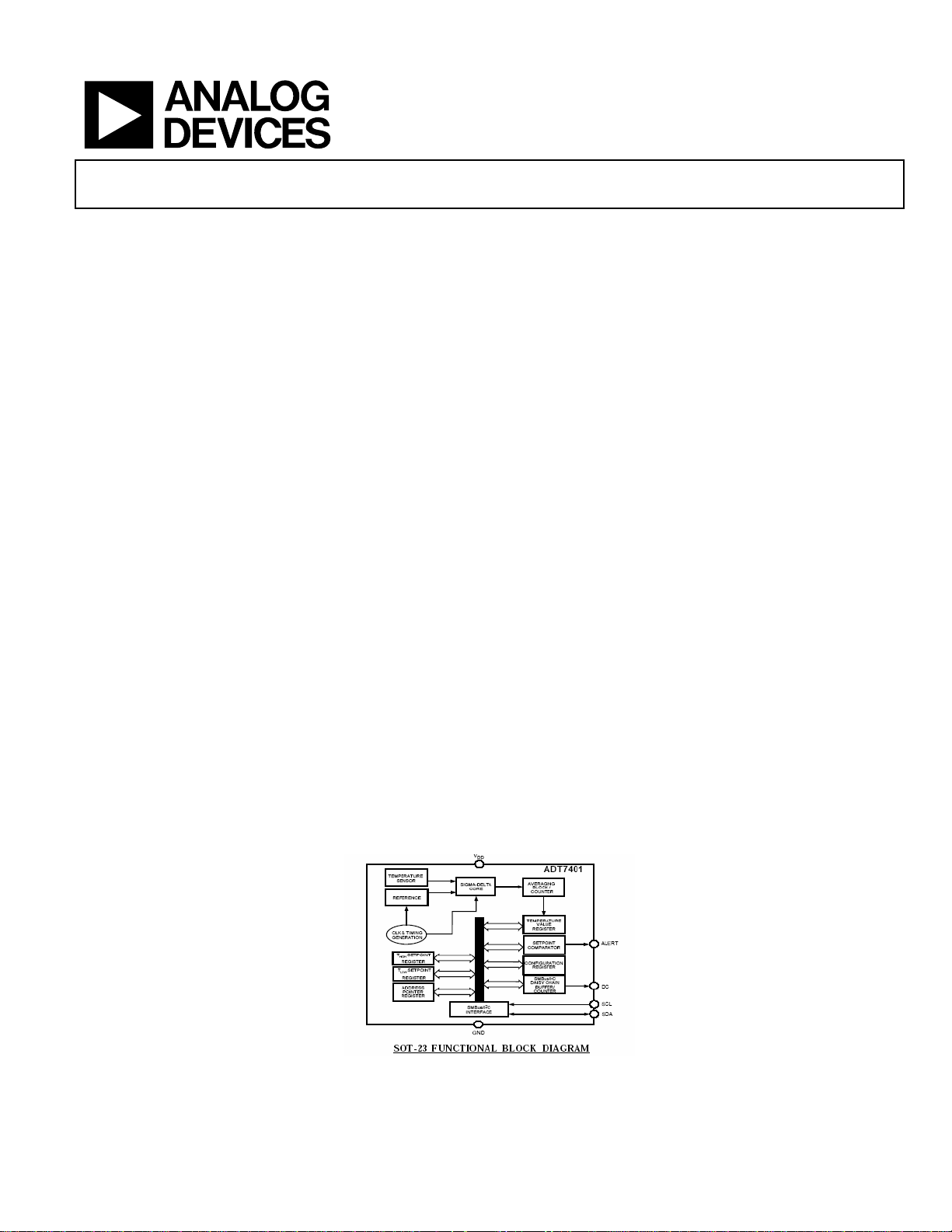
FUNCTIONAL BLOCK DIAGRAM
Figure 1. SOT-23 Functional Block Diagram
Rev. PrE
Information furnished by Analog Devices is believed to be accurate and reliable.
However, no responsibility is assumed by Analog Devices for its use, nor for any
infringements of patents or other rights of third parties that may result from its use.
Specifications subject to change without notice. No license is granted by implication
or otherwise under any patent or patent rights of Analog Devices. Trademarks and
registered trademarks are the property of their respective owners.
One Technology Way, P.O. Box 9106, Norwood, MA 02062-9106, U.S.A.
Tel: 781.329.4700 www.analog.com
Fax: 781.326.8703 © 2004 Analog Devices, Inc. All rights reserved.

ADT7401 Preliminary Technical Data
TABLE OF CONTENTS
Specifications..................................................................................... 3
Application Hints ........................................................................... 10
Timing Characteristics..................................................................... 4
Absolute Maximum Ratings............................................................ 5
ESD Caution.................................................................................. 5
Pin Configuration and Function Descriptions............................. 6
Typical Performance Curves ........................................................... 7
Circuit Information...................................................................... 9
Converter Details.......................................................................... 9
Thermal Response Time ........................................................... 10
Self-Heating Effects.................................................................... 10
Supply Decoupling ..................................................................... 10
Temperature Monitoring........................................................... 10
Outline Dimensions ....................................................................... 11
Ordering Guide .......................................................................... 12
Rev. PrE | Page 2 of 12

Preliminary Technical Data ADT7401
SPECIFICATIONS
All specifications apply for -40°C to +150°C unless otherwise stated. TA = T
Table 1.
Parameter Min Typ Max Units Test Conditions/Comments
TEMPERATURE SENSOR AND ADC
Accuracy @ VDD= +3.3 V (±10%) ±0.5 °C TA= 25°C.
±1 °C TA= 0°C to 70°C.
±2 °C TA= -40°C to +85°C.
±3 °C TA= -40°C to +125°C.
±4
1
°C TA= -40°C to +150°C.
Accuracy @ VDD= +5 V (±10%) ±0.5 °C TA= 25°C.
±1 °C TA= 0°C to 70°C.
±2 °C TA= -40°C to +85°C.
±3 °C TA= -40°C to +125°C.
±41 °C TA= -40°C to +150°C.
Temperature Resolution 0.0625 °C Equivalent to 12 Bits Sigma Delta ADC
Temperature Conversion Time 200 ms
Temperature Update Rtae 1 s Time between each conversion
Long Term Drift 0.25 °C Drift over 10 years if part is operated at +55°C.
Power Supply Rejection Ratio 0.3 0.6 °C/V TA= +25°C
DIGITAL INPUTS2
Input Current ± 1 µA VIN= 0 V to VDD
VIL, Input Low Voltage 0.3×VDD V
VIH, Input High Voltage 0.7×VDD V
Pin Capacitance 3 10 pF All digital inputs
SCL, SDA Glitch Rejection 50 ns Input filtering suppresses noise spikes of less than 50 ns.
DIGITAL OUTPUTS2
VOH, Ouput High Voltage 2.4 V I
VOL, Output Low Voltage 0.4 V IOL= 3 mA
IOH, Output High Current 1 mA VOH= 5 V
C
, Output Capacitance 50 p F
OUT
SUPPLIES
Supply Voltage 2.7 5.5 V
Supply Current Serial Bus Inactive.
Normal Mode6@ 3.3 V 230 450 µA Device Converting.
Normal Mode6@ 5 V 300 500 µA Device Converting.
Quiescent6@ 3.3 V 3 8 µA Device not converting.
Quiescent6@ 5.5 V 5 10 µA Device not converting.
One Shot Mode @ 1 sps 21.16 µA Average Current @ VDD= 2.7 V to 3.6 V.
One Shot Mode @ 1 sps 28.6 µA Average Current @ VDD= 4.5 V to 5.5 V.
Shutdown Current 0.3 1 µA
Power Dissipation 759 µW VDD= +3.3 V, Continuously Converting
Power Dissipation
1 sps 69.83 µW Average Power Dissipated for
V
1 sps 143 µ W Average Power Dissipated for
V
1
It is not recommended to operate the device at temperatures above +125°C for greater than a total of 5% of the lifetime of the device. Any exposure beyond this limit
will affect device reliability.
2
Guaranteed by design and characterization, not production tested.
MIN
to T
SOURCE
, VDD = +2.7 V to +5.5 V, unless otherwise noted
MAX
= I
= 200 µA
SINK
= +3.3 V. One Shot Mode.
DD
= +5 V. One Shot Mode.
DD
Rev. PrE | Page 3 of 12

ADT7401 Preliminary Technical Data
TIMING CHARACTERISTICS
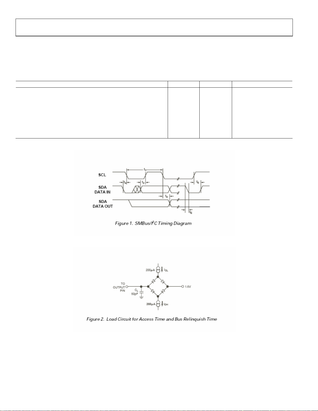
Guaranteed by design and characterization, not production tested. The SDA & SCL timing is measured with the input filters turned on so
as to meet the Fast-Mode I
behaviour of the part. T
Table 2.
Parameter Limit Units Comments
Serial Clock Period, t1 2.5 µs Fast Mode I2C. See Figure 2
Data In Setup Time to SCL High, t2 50 ns
Data Out Stable after SCL Low, t3 0 ns See Figure 2
SDA Low Setup Time to SCL Low
(Start Condition), t4 50 ns See Figure 2
SDA High Hold Time after SCL High
(Stop Condition), t5 50 ns See Figure 2
SDA and SCL Fall Time, t6 90 ns See Figure 2
2
C specification. Switching off the input filters improves the transfer rate but has a negative affect on the EMC
= T
to T
A
MIN
, VDD = +2.7 V to +5.5 V, unless otherwise noted.
MAX
2
Figure 2. SMBus/I
Figure 3. Load Circuit for Access Time and Bus Relinquish Time
C Timing Diagram
Rev. PrE | Page 4 of 12
 Loading...