


±0.25°C Accurate, 16-Bit Digital
ADT7320
Rev. PrD
Preliminary Technical Data
FEATURES
High performance
Temperature accuracy
±0.20°C from −10°C to +85°C at 3.0 V to 3.3V
±0.25°C from −20°C to +105°C at 3.0 V to 3.6 V
16-bit temperature resolution: 0.0078°C
Ultralow temperature drift: 0.0073°C
NIST traceable or equivalent
Fast first temperature conversion on power-up of 6 ms
Easy implementation
No temperature calibration/correction required by user
No linearity correction required
Low power
Power saving 1 sample per second (SPS) mode
700 µW typical at 3.3 V in normal mode
7 µW typical at 3.3 V in shutdown mode
Wide operating ranges
Temperature range: −40°C to +150°C
Voltage range: 2.7 V to 5.5 V
Programmable interrupts
Critical overtemperature interrupt
Overtemperature/undertemperature interrupt
SPI-compatible interface
16-lead, RoHS-compliant, 4 mm × 4 mm LFCSP package
SPI Temperature Sensor
GENERAL DESCRIPTION
The ADT7320 is a high accuracy digital temperature sensor that
o
ffers breakthrough performance over a wide industrial temperature
range, housed in a 4 mm × 4 mm LFCSP package. It contains an
internal band gap reference, a temperature sensor, and a 16-bit
analog-to-digital converter (ADC) to monitor and digitize the
temperature to a resolution of 0.0078°C. The ADC resolution,
by default, is set to 13 bits (0.0625°C). The ADC resolution is a
user programmable mode that can be changed through the
serial interface.
The ADT7320 is guaranteed to operate over supply voltages from
.7 V to 5.5 V. Operating at 3.3 V, the average supply current is
2
typically 210 µA. The ADT7320 has a shutdown mode that powers
down the device and offers a shutdown current of typically 2.0 µA
at 3.3 V. The ADT7320 is rated for operation over the −40°C to
+150°C temperature range.
The CT pin is an open-drain output that becomes active when the
temperature exceeds a programmable critical temperature limit.
The INT pin is also an open-drain output that becomes active
when the temperature exceeds a programmable limit. The INT pin
and CT pin can operate in either comparator or interrupt mode.
APPLICATIONS
RTD and thermistor replacement
Thermocouple cold junction compensation
Medical equipment
Industrial control and test
Food transportation and storage
Environmental monitoring and HVAC
Laser diode temperature control
Information furnished by Analog Devices is believed to be accurate and reliable. However, no
responsibility is assumed by Analog Devices for its use, nor for any infringements of patents or other
rights of third parties that may result from its use. Specifications subject to change without notice. No
license is granted by implication or otherwise under any patent or patent rights of Analog Devices.
Trademarks and registered trademarks are the property of their respective owners.
PRODUCT HIGHLIGHTS
1. Ease of use, no calibration or correction required by the user.
2. Low power consumption.
3. Excellent long term stability and reliability.
4. High accuracy for industrial, instrumentation, and medical
applications.
5. Packaged in a 16-lead, RoHS-compliant, 4 mm × 4 mm
LFCSP package.
One Technology Way, P.O. Box 9106, Norwood, MA 02062-9106, U.S.A.
Tel: 781.329.4700 www.analog.com
Fax: 781.461.3113 ©2011 Analog Devices, Inc. All rights reserved.
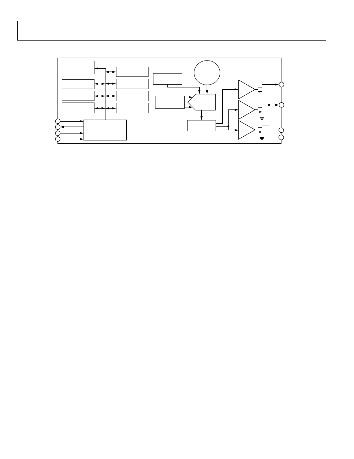
ADT7320 Preliminary Technical Data
DOUT
FUNCTIONAL BLOCK DIAGRAM
SCLK
DIN
CS
TEMPERATURE
VALUE
REGISTER
CONFIGURATION
REGISTER
T
REGISTER
T
REGISTER
1
2
3
4
CRIT
HIGH
SPI
INTERFACE
T
LOW
REGISTER
T
HYST
REGISTER
STATUS
REGISTER
ID
REGISTER
INTERNAL
REFERENCE
TEMPERATURE
SENSOR
INTERNAL
OSCILLATOR
Σ-∆
MODULATOR
FILTER
LOGIC
T
T
T
CRIT
HIGH
LOW
ADT7320
10
CT
9
INT
11
GND
12
V
DD
Figure 1.
Rev. PrD | Page 2 of 26

Preliminary Technical Data ADT7320
TABLE OF CONTENTS
Features ............................................................................................... 1
Applications ....................................................................................... 1
General Description .......................................................................... 1
Product Highlights ............................................................................ 1
Functional Block Diagram ............................................................... 2
Revision History ................................................................................ 3
Specifications ..................................................................................... 4
SPI Timing Specifications ............................................................ 5
Absolute Maximum Ratings ............................................................ 7
ESD Caution .................................................................................. 7
Pin Configuration and Function Descriptions ............................. 8
Typical Performance Characteristics .............................................. 9
Theory of Operation ....................................................................... 11
Circuit Information .................................................................... 11
Converter Details ........................................................................ 11
Continuous Conversion Mode .................................................. 11
One-Shot Mode ........................................................................... 12
1 SPS Mode .................................................................................. 13
Shutdown Mode .......................................................................... 13
Fault Queue .................................................................................. 13
Temperature Data Format .......................................................... 14
Temperature Conversion Formulas .......................................... 14
Registers ............................................................................................ 15
Status Register .............................................................................. 15
Configuration Register ............................................................... 16
Temperature Value Register ....................................................... 17
ID Register ................................................................................... 17
T
Setpoint Register ................................................................ 17
CRIT
T
Setpoint Register ............................................................... 18
HYST
T
Setpoint Register ............................................................... 18
HIGH
T
Setpoint Register ................................................................ 18
LOW
Serial Interface ................................................................................. 19
SPI Command Byte .................................................................... 19
Writing Data ................................................................................ 20
Reading Data ............................................................................... 21
Interfacing to DSPs or Microcontrollers .................................. 21
Serial Interface Reset .................................................................. 21
INT and CT Outputs ...................................................................... 22
Undertemperature and Overtemperature Detection ............. 22
Applications Information ............................................................... 24
Thermal Response Time ............................................................ 24
Supply Decoupling ...................................................................... 24
Powering from a Switching Regulator...................................... 24
Temperature Measurement ........................................................ 24
Quick Guide to Measuring Temperature ................................. 24
Outline Dimensions ........................................................................ 25
Ordering Guide ........................................................................... 25
REVISION HISTORY
11/11— Revision Pr. D: Preliminary Version
Rev. PrD | Page 3 of 26

ADT7320 Preliminary Technical Data
SPECIFICATIONS
TA = −40°C to +125°C, VDD = 2.7 V to 5.5 V, unless otherwise noted.
Table 1.
Parameter Min Typ Max Unit Test Conditions/Comments
TEMPERATURE SENSOR AND ADC
Accuracy
±0.25
±0.30 °C TA = −40°C to +105°C, VDD = 3.0 V
±0.35 °C TA = −40°C to +105°C, VDD = 2.7 V to 3.3 V
±0.50 °C TA = −40°C to +125°C, VDD = 3.0 V to 3.6 V
±0.503 °C TA = −10°C to +105°C, VDD = 4.5 V to 5.5 V
±0.65 °C TA = −40°C to +125°C, VDD = 4.5 V to 5.5 V
−0.85 °C TA = +150°C, VDD = 4.5 V to 5.5 V
−1.0 °C TA = +150°C, VDD = 2.7 V to 3.6 V
ADC Resolution 13 Bits Twos complement temperature value of sign bit plus
16 Bits Twos complement temperature value of sign bit plus
Temperature Resolution
Temperature Conversion Time 240 ms Continuous conversion and one-shot conversion mode
Fast Temperature Conversion Time 6 ms First conversion on power-up only
1 SPS Conversion Time 60 ms Conversion time for 1 SPS mode
Temperature Hysteresis ±0.002 °C Temperature cycle = 25°C to 125°C and back to 25°C
Repeatability
Drift5 0.0073 °C 500 hour stress test at 150°C with VDD = 5.0 V
DC PSRR 0.1 °C/V TA = 25°C
DIGITAL OUTPUTS (CT, INT), OPEN DRAIN
High Output Leakage Current, IOH 0.1 5 µA CT and INT pins pulled up to 5.5 V
Output Low Voltage, VOL 0.4 V IOL = 3 mA at 5.5 V, IOL = 1 mA at 3.3 V
Output High Voltage, VOH 0.7 × VDD V
Output Capacitance, C
DIGITAL INPUTS (DIN, SCLK, CS)
Input Current ±1 µA VIN = 0 V to VDD
Input Low Voltage, VIL 0.4 V
Input High Voltage, VIH 0.7 × VDD V
Pin Capacitance 5 10 pF
DIGITAL OUTPUT (DOUT)
Output High Voltage, VOH VDD − 0.3 V I
Output Low Voltage, V
Output Capacitance, C
POWER REQUIREMENTS
Supply Voltage 2.7 5.5 V
Supply Current Peak current while converting, SPI interface inactive
1 SPS Current 1 SPS mode, TA = 25°C
1
0.0017 ±0.202 °C TA = −10°C to +85°C, VDD = 3.0 V to 3.3V
°C TA = −20°C to +105°C, VDD = 3.0 V to 3.6 V
±0.25
TA = −20°C to +85°C, VDD = 2.7 V
12 ADC bits (power-up default resolution)
15 ADC bits (Bit 7 = 1 in the configuration register)
13-Bit 0.0625 °C 13-bit resolution (sign + 12 bits)
16-Bit 0.0078 °C 16-bit resolution (sign + 15 bits)
4
OUT
OL
50 pF
OUT
±0.015 °C TA = 25°C
2 pF
= I
SOURCE
SINK
0.4 V IOL = 200 µA
= 200 µA
At 3.3 V 210 265 µA
At 5.5 V 250 300 µA
Rev. PrD | Page 4 of 26
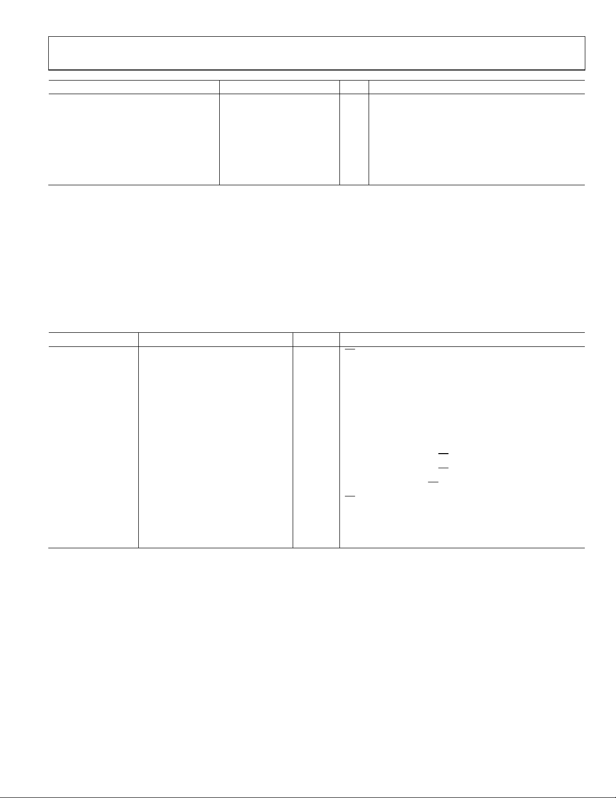
Preliminary Technical Data ADT7320
Parameter Min Typ Max Unit Test Conditions/Comments
At 3.3 V 46 µA VDD = 3.3 V
At 5.5 V 65 µA VDD = 5.5 V
Shutdown Current Supply current in shutdown mode
At 3.3 V 2.0 15 µA
At 5.5 V 5.2 25 µA
Power Dissipation, Normal Mode 700 µW VDD = 3.3 V, normal mode at 25°C
Power Dissipation, 1 SPS Mode 150 µW Power dissipated for VDD = 3.3 V, TA = 25°C
1
Accuracy specification includes repeatability.
2
The equivalent 3 σ limits are ±0.15°C. This 3 σ specification is provided to enable comparison with other vendors who use these limits.
3
For higher accuracy at 5 V operation, contact Analog Devices, Inc.
4
Based on a floating average of 10 readings.
5
Drift includes solder heat resistance and lifetime test performed as per JEDEC Standard JESD22-A108.
SPI TIMING SPECIFICATIONS
TA = −40°C to +150°C, VDD = 2.7 V to 5.5 V, unless otherwise noted. All input signals are specified with rise time (tR) = fall time (tF) = 5 ns
(10% to 90% of VDD) and timed from a voltage level of 1.6 V.
Table 2.
Parameter
t1 0 ns min
t2 100 ns min SCLK high pulse width
t3 100 ns min SCLK low pulse width
t4 30 ns min Data setup time prior to SCLK rising edge
t5 25 ns min Data hold time after SCLK rising edge
t6 5 ns min Data access time after SCLK falling edge
60 ns max VDD = 4.5 V to 5.5 V
80 ns max VDD = 2.7 V to 3.6 V
3
t
10 ns min Bus relinquish time after CS inactive edge
7
80 ns max Bus relinquish time after CS inactive edge
t8 0 ns min SCLK inactive edge to CS rising edge hold time
t9 0 ns min
60 ns max VDD = 4.5 V to 5.5 V
80 ns max VDD = 2.7 V to 3.6 V
t10 10 ns min SCLK inactive edge to DOUT low
1
Sample tested during initial release to ensure compliance.
2
See Error! Reference source not found..
3
This means that the times quoted in the timing characteristics in Table 2 are the true bus relinquish times of the part and, as such, are independent of external bus
loading capacitances.
1, 2
Limit at T
MIN
, T
Unit Descriptions
MAX
CS
CS
falling edge to SCLK active edge setup time
falling edge to DOUT active time
Rev. PrD | Page 5 of 26
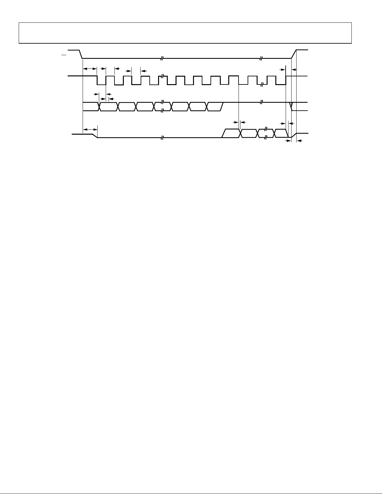
ADT7320 Preliminary Technical Data
DOUT
CS
t
1
t
SCLK
DIN
2
1
t
4
t
MSB LSB
t
9
5
t
3
2 3
9 10 23 24
876
t
6
MSB
Figure 2. Detailed SPI Timing Diagram
t
8
t
10
LSB
t
7
09012-002
Rev. PrD | Page 6 of 26
Preliminary Technical Data ADT7320
ABSOLUTE MAXIMUM RATINGS
Table 3.
Parameter Rating
VDD to GND −0.3 V to +7 V
DIN Input Voltage to GND −0.3 V to VDD + 0.3 V
DOUT Voltage to GND −0.3 V to VDD + 0.3 V
SCLK Input Voltage to GND −0.3 V to VDD + 0.3 V
Input Voltage to GND −0.3 V to VDD + 0.3 V
CS
CT and INT Output Voltage to GND −0.3 V to VDD + 0.3 V
ESD Rating (Human Body Model) 2.0 kV
Operating Temperature Range
1
−40°C to +150°C
Storage Temperature Range −65°C to +160°C
Maximum Junction Temperature, T
150°C
JMAX
Power Dissipation2
16-Lead LFCSP3 W
MAX
= (T
− TA)/θJA
JMAX
Thermal Impedance4
θJA, Junction-to-Ambient (Still Air) 37°C/W
θJC, Junction-to-Case 33°C/W
IR Reflow Soldering 220°C
Peak Temperature (RoHS-Compliant
260°C (0°C/−5°C)
Package)
Time at Peak Temperature 20 sec to 40 sec
Ramp-Up Rate 3°C/sec maximum
Ramp-Down Rate −6°C/sec maximum
Time from 25°C to Peak Temperature 8 minutes maximum
1
Sustained operation above 125°C results in a shorter product lifetime. For
more information, contact an Analog Devices, Inc., sales representative.
2
Values relate to package being used on a standard 2-layer PCB. This gives a
worst-case θJA and θJC.
3
TA = ambient temperature.
4
Junction-to-case resistance is applicable to components featuring a
preferential flow direction, for example, components mounted on a heat
sink. Junction-to-ambient resistance is more useful for air cooled, PCBmounted components.
Stresses above those listed under Absolute Maximum Ratings
may cause permanent damage to the device. This is a stress
rating only; functional operation of the device at these or any
other conditions above those indicated in the operational
section of this specification is not implied. Exposure to absolute
maximum rating conditions for extended periods may affect
device reliability.
ESD CAUTION
Rev. PrD | Page 7 of 26
ADT7320 Preliminary Technical Data
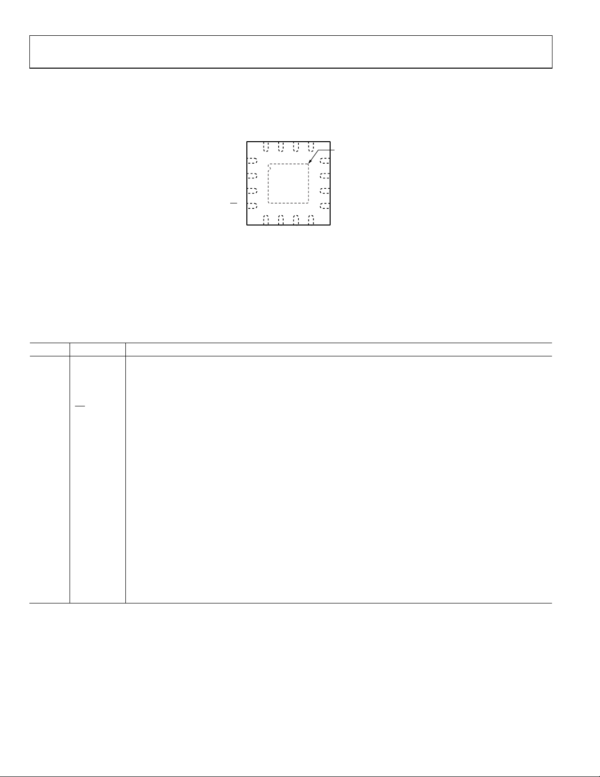
N
C
PIN CONFIGURATION AND FUNCTION DESCRIPTIONS
C
C
N
6
5
1
1
1
SCLK
2
DOUT
3
DIN
4
CS
NOTES
1. NC = NO CONNECT. DO NOT CONNECT TO THIS PIN.
THE NC PIN IS NOT BONDED TO THE DIE INTERNALLY.
2. TO ENSURE CORRECT OPERATION, THE EXPOSED PAD
SHOULD EITHER BE LEFT FLOATING OR CONNECTED
TO GROUND.
ADT7320
TOP VIEW
(Not to Scale)
6
5
C
C
N
N
Figure 3. Pin Configuration
Table 4. Pin Function Descriptions
Pin No. Mnemonic Description
1 SCLK Serial Clock Input. The serial clock is used to clock data into and out of any register of the ADT7320.
2 DOUT Serial Data Output. Data is clocked out on the SCLK falling edge and is valid on the SCLK rising edge.
3 DIN Serial Data Input. Serial data to be loaded to the control registers of the part is provided on this input. Data is
clocked into the registers on the rising edge of SCLK.
4
CS
Chip Select Input. The device is enabled when this input is low. The device is disabled when this pin is high.
5 NC No Connect. Do not connect to this pin. The NC pin is not bonded to the die internally.
6 NC No Connect. Do not connect to this pin. The NC pin is not bonded to the die internally.
7 NC No Connect. Do not connect to this pin. The NC pin is not bonded to the die internally.
8 NC No Connect. Do not connect to this pin. The NC pin is not bonded to the die internally.
9 INT Overtemperature and Undertemperature Interrupt. Logic output. Power-up default setting is as an active low
comparator interrupt. Open-drain configuration. A pull-up resistor is required, typically 10 kΩ.
10 CT Critical Overtemperature Interrupt. Logic output. Power-up default polarity is active low. Open-drain
configuration. A pull-up resistor is required, typically 10 kΩ.
11 GND Analog and Digital Ground.
12 VDD Positive Supply Voltage (2.7 V to 5.5 V). Decouple the supply with a 0.1 µF ceramic capacitor to GND.
13 NC No Connect. Do not connect to this pin. The NC pin is not bonded to the die internally.
14 NC No Connect. Do not connect to this pin. The NC pin is not bonded to the die internally.
15 NC No Connect. Do not connect to this pin. The NC pin is not bonded to the die internally.
16 NC No Connect. Do not connect to this pin. The NC pin is not bonded to the die internally.
17 EPAD Exposed Pad. To ensure correct operation, the exposed pad should either be left floating or connected to ground.
C
N
N
3
4
1
1
17 EPAD
12
V
DD
11
GND
10
CT
9
INT
8
7
C
C
N
N
09012-003
Rev. PrD | Page 8 of 26
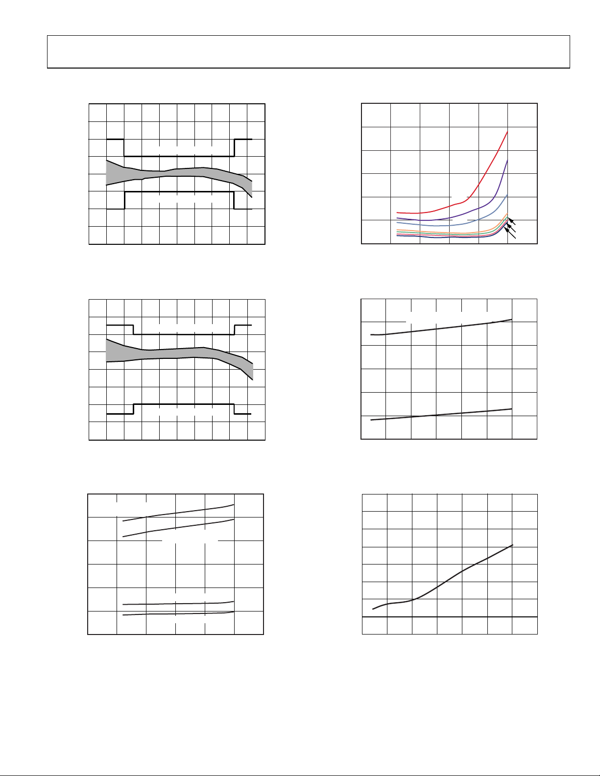
Preliminary Technical Data ADT7320
TEMPERATURE ERROR (°C)
1.00
TEMPER
A
TURE ERROR (°C)
1.00
I
(µA)
300
SHUTDOWN I
(µA)
30
300
I
(µA)
8
SHUTDOWN
IDD(µA
)
TYPICAL PERFORMANCE CHARACTERISTICS
0.75
0.50
0.25
–0.25
–0.50
–0.75
–1.00
0.75
0.50
0.25
–0.25
–0.50
–0.75
0
–40–60 –20 0 20 40
Figure 4. Temperature Accuracy at 3 V
0
MAX ACCURACY LIMITS
MAX ACCURAC Y LIMITS
60 80 100 120 140
TEMPERATURE (°C)
MAX ACCURAC Y LIMITS
MAX ACCURACY LIMIT S
25
20
DD
15
10
5
0
–100 –50 0 50 100 150 200
09012-027
TEMPERATURE (°C)
5.5V
5.0V
4.5V
3.6V
3.3V
3.0V
2.7V
09012-032
Figure 7. Shutdown Current vs. Temperature
250
200
150
DD
100
50
CONTINUOUS CONVERSION
1SPS
–1.00
–40–60 –20 0 20 40
TEMPERATURE (°C)
60 80 100 120 140
Figure 5. Temperature Accuracy at 5 V
5.5V CONTINUOUS
CONVERSION
250
3.0V CONTINUOUS
200
150
DD
100
50
0
–100 –50 0 50 100 150 200
CONVERSION
5.5V 1SPS
3.0V 1SPS
TEMPERATURE (°C)
Figure 6. Operating Supply Current vs. Temperature
0
2.5 3.0 3.5 4.0 4.5 5.0 5.5 6.0
09012-026
SUPPLY VOLTAGE (V)
09012-029
Figure 8. Average Operating Supply Current vs. Supply Voltage
7
6
5
4
3
2
1
0
2.5 3.0 3.5 4.0 4.5 5.0 5.5 6.0
09012-028
SUPPLY VOLTAGE (V)
09012-210
Figure 9. Shutdown Current vs. Supply Voltage
Rev. PrD | Page 9 of 26

ADT7320 Preliminary Technical Data
140
DUT TEMPER
A
TURE (°C)
120
100
125°C
105°C
80
60
40
20
IT TAKES LESS THAN 2 SECONDS
FOR THE DUT TO REACH 63.2%
OF ITS FINAL TEMPERATURE SPAN
85°C
0
0 5 10 15 2520
TIME (s)
Figure 10. Thermal Response Time
110
Rev. PrD | Page 10 of 26

Preliminary Technical Data ADT7320
THEORY OF OPERATION
CIRCUIT INFORMATION
The ADT7320 is a high accuracy digital temperature sensor that
uses a 16-bit ADC to monitor and digitize the temperature to a
resolution of 0.0078°C. By default, the ADC resolution is set to
13 bits (0.0625°C). An internal temperature sensor generates a
voltage proportional to absolute temperature; this voltage is
compared to an internal voltage reference and input into a
precision digital modulator.
The internal temperature sensor has high accuracy and linearity
over the entire rated temperature range without the need for
correction or calibration by the user.
The sensor output is digitized by a sigma-delta (Σ-∆) modulator,
also known as the charge balance type ADC. This type of converter
uses time domain oversampling and a high accuracy comparator to
deliver 16 bits of resolution in an extremely compact circuit.
CONVERTER DETAILS
The Σ-∆ modulator consists of an input sampler, a summing
network, an integrator, a comparator, and a 1-bit digital-to-analog
converter (DAC). This architecture creates a negative feedback
loop and minimizes the integrator output by changing the duty
cycle of the comparator output in response to the input voltage
changes. The comparator samples the output of the integrator at
a much higher rate than the input sampling frequency. This
oversampling spreads the quantization noise over a much wider
band than that of the input signal, improving overall noise
performance and increasing accuracy.
The modulated output of the comparator is encoded using a
circuit technique that results in SPI temperature data.
Σ-∆ MODULATOR
VOLTAGE
REFERENCE
INTEGRATOR
COMPARATOR
The ADT7320 can be configured to operate in any one of the
f
ollowing four operating modes: normal mode, one-shot mode,
1 SPS mode, and shutdown mode.
CONTINUOUS CONVERSION MODE
In continuous conversion mode (default power-up mode), the
ADT7320 runs an automatic conversion sequence. During this
utomatic conversion sequence, a conversion takes 240 ms to
a
complete and the ADT7320 is continuously converting. This means
that as soon as one temperature conversion is completed, another
temperature conversion begins. Each temperature conversion
result is stored in the temperature value register and is available
through the SPI interface. In continuous conversion mode, the
read operation provides the most recent converted result.
On power-up, the first conversion is a fast conversion, taking
typically 6 ms. If the temperature exceeds 147°C, the CT pin is
asserted low. If the temperature exceeds 64°C, the INT pin is
asserted low. Fast conversion temperature accuracy is typically
within ±5°C.
The conversion clock for the part is generated internally. No
external clock is required except when reading from and writing
to the serial port.
The measured temperature value is compared with a critical
temperature limit (stored in the 16-bit T
high temperature limit (stored in the 16-bit T
register), and a low temperature limit (stored in the 16-bit T
setpoint register). If the measured value exceeds the high or low
temperature limits, the INT pin is activated; if it exceeds the T
limit, the CT pin is activated. The polarity of the INT and CT
pins is programmable for via the configuration register, and the
INT and CT pins are also programmable for interrupt mode via
the configuration register.
setpoint register), a
CRIT
setpoint
HIGH
LOW
CRIT
1-BIT
DAC
1-BIT
13-/16-BIT
TEMPERATURE
VALUE
REGISTER
09012-012
CLOCK
GENERATOR
LPF DIGITAL
FILTER
Figure 11. Σ-∆ Modulator
Rev. PrD | Page 11 of 26

ADT7320 Preliminary Technical Data
TEMPERATURE
CS
DIN
DOUT
SCLK
0x08 0x20
WAIT 240ms MINIMUM
FOR CONVERSION TO FINISH
DATA
Figure 12. Typical SPI One-Shot Write to Configuration Register Followed by a Read from the Temperature Value Register
149°C
148°C
147°C
146°C
145°C
144°C
143°C
142°C
141°C
140°C
POLARITY = ACTIVE LOW
POLARITY = ACTIVE HIGH
*THERE IS A 240ms DELAY BETWEEN WRITING TO THE CONFIGURATION REGISTER TO START
A STANDARD ONE-SHOT CONVERSION AND THE CT PIN GOING ACTIVE. THIS IS DUE TO THE
CONVERSION TIME. THE DELAY IS 60ms IN THE CASE OF A ONE-SHOT CONVERSION.
CT PIN
CT PIN
WRITE TO
BIT 5 AND BIT 6 OF
CONFIGURATION
REGISTER.*
WRITE TO
BIT 5 AND BIT 6 OF
CONFIGURATION
REGISTER.*
BIT 5 AND BIT 6 OF
CONFIGURATION
WRITE TO
REGISTER.*
T
CRIT
T
– T
CRIT
HYST
TIME
Figure 13. One-Shot CT Pin
09012-300
ONE-SHOT MODE
When one-shot mode is enabled, the ADT7320 immediately
completes a conversion and then goes into shutdown mode. The
one-shot mode is useful when one of the circuit design priorities is
to reduce power consumption.
To enable one-shot mode, set Bits [6:5] of the configuration
register (Register Address 0x01) to 01.
After writing to the operation mode bits, wait for at least 240 ms
before reading back the temperature from the temperature value
register. This delay ensures that the ADT7320 has adequate time
o power up and complete a conversion.
t
To obtain an updated temperature conversion, reset Bits[6:5] of the
configuration register (Register Address 0x01) to 01.
Rev. PrD | Page 12 of 26
CT and INT Operation in One-Shot Mode
See Figure 13 for more information on one-shot CT pin
operation for T
overtemperature events when one of the
CRIT
limits is exceeded. Note that in interrupt mode, a read from
any register resets the INT and CT pins.
For the INT pin in comparator mode, if the temperature drops
below the T
HIGH
− T
value or goes above the T
HYST
LOW
+ T
HYST
value,
a write to the operation mode bits (Bit 5 and Bit 6 of the
configuration register, Register Address 0x01) resets the INT pin.
For the CT pin in comparator mode, if the temperature drops
below the T
CRIT
− T
value, a write to the operation mode bits
HYST
(Bit 5 and Bit 6 of the configuration register, Register Address 0x01)
resets the CT pin (see Figure 13).

Preliminary Technical Data ADT7320
When using one-shot mode, ensure that the refresh rate is
appropriate to the application being used.
When the part is taken out of shutdown mode, the internal clock
restarts and a conversion is initiated.
1 SPS MODE
In 1 SPS mode, the part performs one measurement per second.
A conversion takes 60 ms typically, and the part remains in the
idle state for the remaining 940 ms period. This mode is
enabled by setting Bits[6:5] of the configuration register
(Register Address 0x01) to 10.
SHUTDOWN MODE
The ADT7320 can be placed in shutdown mode by setting
its[6:5] of the configuration register (Register Address 0x01) to
B
11. The ADT7320 can be taken out of shutdown mode by setting
Bits[6:5] of the configuration register (Register Address 0x01) to
00. The ADT7320 typically takes 1 ms (with a 0.1 µF decoupling
capacitor) to come out of shut-down mode. The conversion
result from the last conversion prior to shutdown can still be
read from the ADT7320 even when it is in shutdown mode.
FAULT QUEUE
Bit 0 and Bit 1 of the configuration register (Register Address 0x01)
are used to set up a fault queue. Up to four faults are provided to
prevent false tripping of the INT and CT pins when the ADT7320
i
s used in a noisy temperature environment. The number of
faults set in the queue must occur consecutively to set the INT
and CT outputs. For example, if the number of faults set in the
queue is four, then four consecutive temperature conversions
must occur, with each result exceeding a temperature limit set in
any of the limit registers, before the INT and CT pins are activated.
If two consecutive temperature conversions exceed a temperature
limit and the third conversion does not, the fault count is reset to
zero.
Rev. PrD | Page 13 of 26

ADT7320 Preliminary Technical Data
TEMPERATURE DATA FORMAT
One LSB of the ADC corresponds to 0.0625°C in 13-bit mode or
0.0078°C in 16-bit mode. The ADC can theoretically measure a
temperature range of 255°C, but the ADT7320 is guaranteed to
measure a low value temperature limit of −40°C to a high value
temperature limit of +150°C. The temperature measurement
result is stored in the 16-bit temperature value register and is
compared with the high temperature limits stored in the T
setpoint register and the T
with the low temperature limit stored in the T
setpoint register. It is also compared
HIGH
setpoint register.
LOW
CRIT
TEMPERATURE CONVERSION FORMULAS
16-Bit Temperature Data Format
Positive Temperature = ADC Code (dec)/128
Negative Temperature = (ADC Code (dec) − 65,536)/128
where ADC Code uses all 16 bits of the data byte, including the
sign bit.
Negative Temperature = (ADC Code (dec) − 32,768)/128
where the MSB is removed from the ADC code.
Temperature data in the temperature value register, the T
setpoint register, the T
setpoint register, and the T
HIGH
LOW
CRIT
setpoint register are represented by a 13-bit, twos complement
word. The MSB is the temperature sign bit. On power-up the three
LSBs, Bit 0 to Bit 2, are not part of the temperature conversion
result and are flag bits for T
CRIT
, T
HIGH
, and T
. Table 5 shows
LOW
the 13-bit temperature data format without Bit 0 to Bit 2.
The number of bits in the temperature data-word can be extended
to 16 bits, twos complement by setting Bit 7 to 1 in the configuration
register (Register Address 0x01). When using a 16-bit temperature
data value, Bit 0 to Bit 2 are not used as flag bits and are instead
the LSB bits of the temperature value. The power-on default
setting has a 13-bit temperature data value.
Reading back the temperature from the temperature value register
requires a 2-byte read. Designers that use a 9-bit temperature
data format can still use the ADT7320 by ignoring the last four
SBs of the 13-bit temperature value. These four LSBs are Bit 3
L
to Bit 6 in Table 5.
Table 5. 13-Bit Temperature Data Format
Temperature Digital Output (Binary) Bits[15:3]
−40°C 1 1101 1000 0000
−25°C 1 1110 0111 0000
−0.0625°C 1 1111 1111 1111
0°C 0 0000 0000 0000
+0.0625°C 0 0000 0000 0001
+25°C 0 0001 1001 0000
+105°C 0 0110 1001 0000
+125°C 0 0111 1101 0000
+150°C 0 1001 0110 0000
13-Bit Temperature Data Format
Positive Temperature = ADC Code (dec)/16
Negative Temperature = (ADC Code (dec) − 8192)/16
where ADC Code uses all 13 bits of the data byte, including the
sign bit.
Negative Temperature = (ADC Code (dec) − 4096)/16
where the MSB is removed from the ADC code.
10-Bit Temperature Data Format
Positive Temperature = ADC Code (dec)/2
Negative Temperature = (ADC Code (dec) − 1024)/2
where ADC Code uses all 10 bits of the data byte, including the
sign bit.
Negative Temperature = (ADC Code (dec) − 512)/2
where the MSB is removed from the ADC Code.
9-Bit Temperature Data Format
Positive Temperature = ADC Code (dec)
Negative Temperature = ADC Code (dec) − 512
where ADC Code uses all nine bits of the data byte, including
the sign bit.
Negative Temperature = ADC Code (dec) − 256
where the MSB is removed from the ADC Code.
Rev. PrD | Page 14 of 26

Preliminary Technical Data ADT7320
REGISTERS
The ADT7320 contains eight registers:
• A status register
• A configuration register
• Five temperature registers
• An ID register
The status register, temperature value register, and the ID
register are read only.
Table 6. ADT7320 Registers
egister Address Description Power-On Default
R
0x00 Status 0x80
0x01 Configuration 0x00
0x02 Temperature value 0x0000
0x03 ID 0xC3
0x04 T
0x05 T
0x06 T
0x07 T
setpoint 0x4980 (147°C)
CRIT
setpoint 0x05 (5°C)
HYST
setpoint 0x2000 (64°C)
HIGH
setpoint 0x0500 (10°C)
LOW
Table 7. Status Register (Register Address 0x00)
Default
Bit(s)
Value Type Name Description
[3:0] 0000 R Unused Reads back 0.
[4] 0 R T
This bit is set to 1 when the temperature goes below the T
LOW
0 when the status register is read and/or when the temperature measured rises above the limit set
[5] 0 R T
in the T
This bit is set to 1 when the temperature rises above the T
HIGH
LOW
+ T
setpoint registers.
HYST
to 0 when the status register is read and/or when the temperature measured drops below the limit
[6] 0 R T
set in the T
This bit is set to 1 when the temperature rises above the T
CRIT
HIGH
− T
HYST
0 when the status register is read and/or when the temperature measured drops below the limit set
[7] 1 R
RDY
in the T
This bit goes low when the temperature conversion result is written to the temperature value
CRIT
− T
setpoint registers.
HYST
register. It is reset to 1 when the temperature value register is read. In one-shot and 1 SPS modes,
this bit is reset after a write to the operation mode bits in the configuration register.
STATUS REGISTER
This 8-bit read-only register (Register Address 0x00) reflects the
status of the overtemperature and undertemperature interrupts
that can cause the CT and INT pins to become active. It also
reflects the status of a temperature conversion operation. The
interrupt flags in this register are reset by a read operation to
the status register and/or when the temperature value returns
within the temperature limits including hysteresis. The
reset after a read from the temperature value register. In oneshot and 1 SPS modes, the
operation mode bits in the configuration register.
setpoint registers.
RDY
RDY
bit is reset after a write to the
temperature limit. The bit is cleared to
LOW
temperature limit. This bit is cleared
HIGH
temperature limit. This bit is cleared to
CRIT
bit is
Rev. PrD | Page 15 of 26

ADT7320 Preliminary Technical Data
CONFIGURATION REGISTER
This 8-bit read/write register (Register Address 0x01) stores various
configuration modes for the ADT7320, including shutdown,
overtemperature and undertemperature interrupts, one-shot,
continuous conversion, interrupt pin polarity, and
overtemperature fault queues.
Table 8. Configuration Register (Register Address 0x01)
Default
Bit(s)
[1:0] 00 R/W Fault queue These two bits set the number of undertemperature/overtemperature faults that can
00 = 1 fault (default).
01 = 2 faults.
10 = 3 faults.
11 = 4 faults.
[2] 0 R/W CT pin polarity This bit selects the output polarity of the CT pin.
0 = active low.
1 = active high.
[3] 0 R/W INT pin polarity This bit selects the output polarity of the INT pin.
0 = active low.
1 = active high.
[4] 0 R/W INT/CT mode This bit selects comparator mode or interrupt mode.
0 = interrupt mode.
1 = comparator mode.
[6:5] 00 R/W Operation mode These two bits set the operational mode of the ADT7320.
00 = continuous conversion (default). When one conversion is finished, the ADT7320
01 = one-shot mode. Conversion time is typically 240 ms.
10 = 1 SPS mode. Conversion time is typically 60 ms. This operational mode reduces the
11 = shutdown. All circuitry except for the interface circuitry is powered down.
[7] 0 R/W Resolution This bit sets the resolution of the ADC when converting.
0 = 13-bit resolution. Sign bit + 12 bits gives a temperature resolution of 0.0625°C.
1 = 16-bit resolution. Sign bit + 15 bits gives a temperature resolution of 0.0078°C.
Value
Type Name Description
occur before setting the INT and CT pins. This helps to avoid false triggering due to
temperature noise.
begins the next conversion.
average current consumption.
Rev. PrD | Page 16 of 26

Preliminary Technical Data ADT7320
TEMPERATURE VALUE REGISTER
The temperature value register stores the temperature measured
by the internal temperature sensor. The temperature is stored in
a 16-bit, twos complement format. The temperature is read back
from the temperature value register (Register Address 0x02) as a
16-bit value.
Bit 2, Bit 1, and Bit 0 are event alarm flags for T
T
, respectively. When the ADC is configured to convert the
LOW
temperature to a 16-bit digital value, Bit 2, Bit 1, and Bit 0 are
no longer used as flag bits and are, instead, used as the LSB bits for
the extended digital value.
CRIT
, T
HIGH
, and
ID REGISTER
This 8-bit read-only register (Register Address 0x03) stores
the manufacturer ID in Bit 7 to Bit 3 and the silicon revision in
Bit 2 to Bit 0.
T
SETPOINT REGISTER
CRIT
The 16-bit T
the critical overtemperature limit value. A critical overtemperature
event occurs when the temperature value stored in the temperature
value register exceeds the value stored in this register. The CT
pin is activated if a critical overtemperature event occurs. The
temperature is stored in twos complement format with the MSB
being the temperature sign bit.
setpoint register (Register Address 0x04) stores
CRIT
The default setting for the T
setpoint is 147°C.
CRIT
Table 9. Temperature Value Register (Register Address 0x02)
Bit(s) Default Value Type Name Description
[0] 0 R T
flag/LSB0 Flags a T
LOW
(13-bit resolution). When the temperature value is below T
event if the configuration register, Register Address 0x01[7] = 0
LOW
, this bit is set to 1.
LOW
Contains Least Significant Bit 0 of the 15-bit temperature value when the
configuration register, Register Address 0x01[7] = 1 (16-bit resolution).
[1] 0 R T
flag/LSB1 Flags a T
HIGH
event if the configuration register, Register Address 0x01[7] = 0
HIGH
(13-bit resolution). When the temperature value is above T
, this bit is set to 1.
HIGH
Contains Least Significant Bit 1 of the 15-bit temperature value when the
configuration register, Register Address 0x01[7] = 1 (16-bit resolution).
[2] 0 R T
flag/LSB2 Flags a T
CRIT
(13-bit resolution). When the temperature value exceeds T
event if the configuration register, Register Address 0x01[7] = 0
CRIT
, this bit is set to 1.
CRIT
Contains the Least Significant Bit 2 of the 15-bit temperature value if the
configuration register, Register Address 0x01[7] = 1 (16-bit resolution).
[7:3] 00000 R Temp Temperature value in twos complement format.
[14:8] 0000000 R Temp Temperature value in twos complement format.
15 0 R Sign Sign bit; indicates if the temperature value is negative or positive.
Table 10. ID Register (Register Address 0x03)
Bit(s) Default Value Type Name Description
[2:0] 011 R Revision ID Contains the silicon revision identification number.
[7:3] 11000 R Manufacturer ID Contains the manufacturer identification number.
Table 11. T
Setpoint Register (Register Address 0x04)
CRIT
Bit(s) Default Value Type Name Description
[15:0] 0x4980 R/W T
16-bit critical overtemperature limit, stored in twos complement format.
CRIT
Rev. PrD | Page 17 of 26

ADT7320 Preliminary Technical Data
T
SETPOINT REGISTER
T
SETPOINT REGISTER
HYST
The 8-bit T
the temperature hysteresis value for the T
setpoint register (Register Address 0x05) stores
HYST
, T
LOW
, and T
HIGH
CRIT
temperature limits. The temperature hysteresis value is stored in
straight binary format using the four LSBs. Increments are possible
in steps of 1°C from 0°C to 15°C. The value in this register is
subtracted from the T
T
value to implement hysteresis.
LOW
HIGH
and T
values and added to the
CRIT
LOW
The 16-bit T
setpoint register (Register Address 0x07) stores
LOW
the undertemperature limit value. An undertemperature event
occurs when the temperature value stored in the temperature
value register is less than the value stored in this register. The
INT pin is activated if an undertemperature event occurs. The
temperature is stored in twos complement format with the MSB
being the temperature sign bit.
The default setting for the T
T
SETPOINT REGISTER
HIGH
The 16-bit T
setpoint register (Register Address 0x06) stores
HIGH
setpoint is 5°C.
HYST
the overtemperature limit value. An overtemperature event occurs
when the temperature value stored in the temperature value
register exceeds the value stored in this register. The INT pin is
activated if an overtemperature event occurs. The temperature
is stored in twos complement format with the most significant
bit being the temperature sign bit.
The default setting for the T
Table 12. T
Setpoint Register (Register Address 0x05)
HYST
Bit(s) Default Value Type Name
[3:0]
[7:4]
Table 13. T
0101 R/W T
0000 R/
Setpoint Register (Register Address 0x06)
HIGH
setpoint is 64°C.
HIGH
Description
Hysteresis value, from 0°C to 15°C. Stored in straight binary format. The default setting is 5°C.
HYST
N/A N/A = not applicable. Not used.
W
Bit(s) Default Value Type Name Description
[15:0] 0x2000 R/W T
Table 14. T
Setpoint Register (Register Address 0x07)
LOW
16-bit overtemperature limit, stored in twos complement format.
HIGH
Bit(s) Default Value Type Name Description
[15:0] 0x0500 R/W T
16-bit undertemperature limit, stored in twos complement format.
LOW
The default setting for the T
setpoint is 10°C.
LOW
Rev. PrD | Page 18 of 26
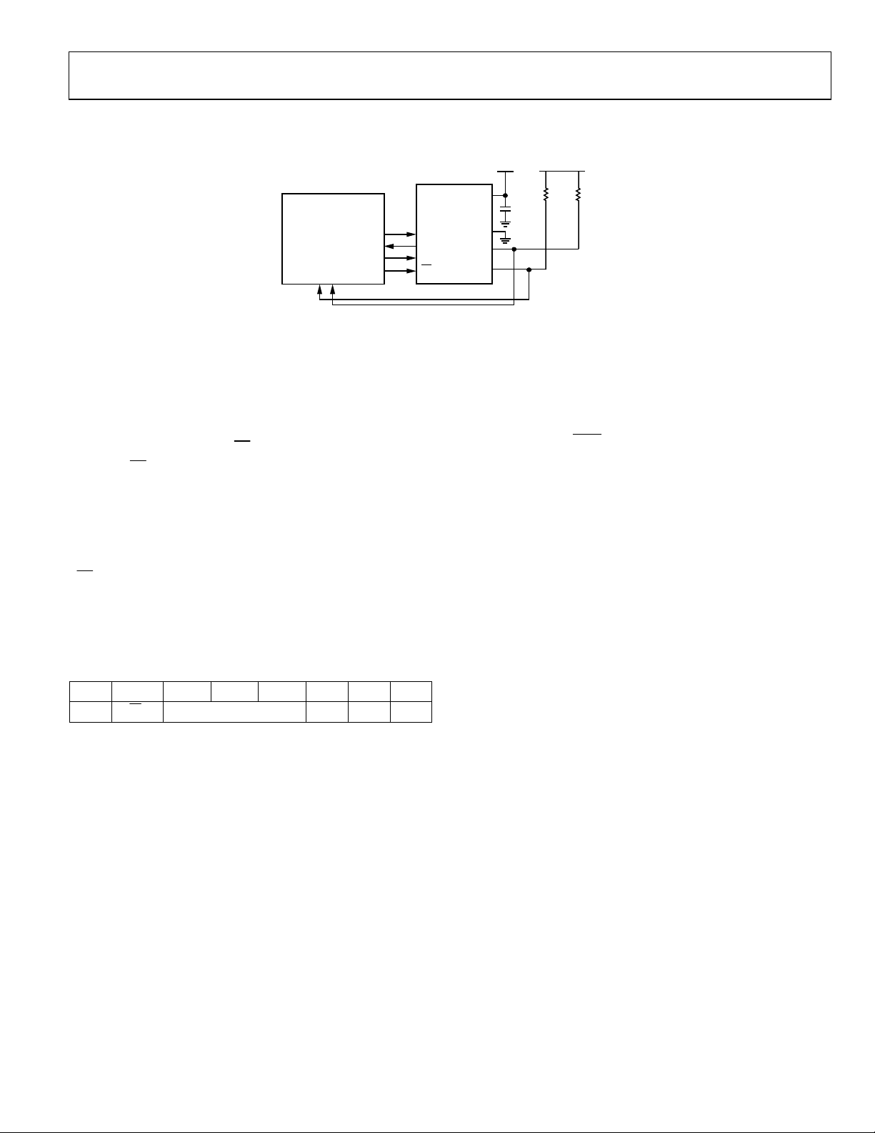
Preliminary Technical Data ADT7320
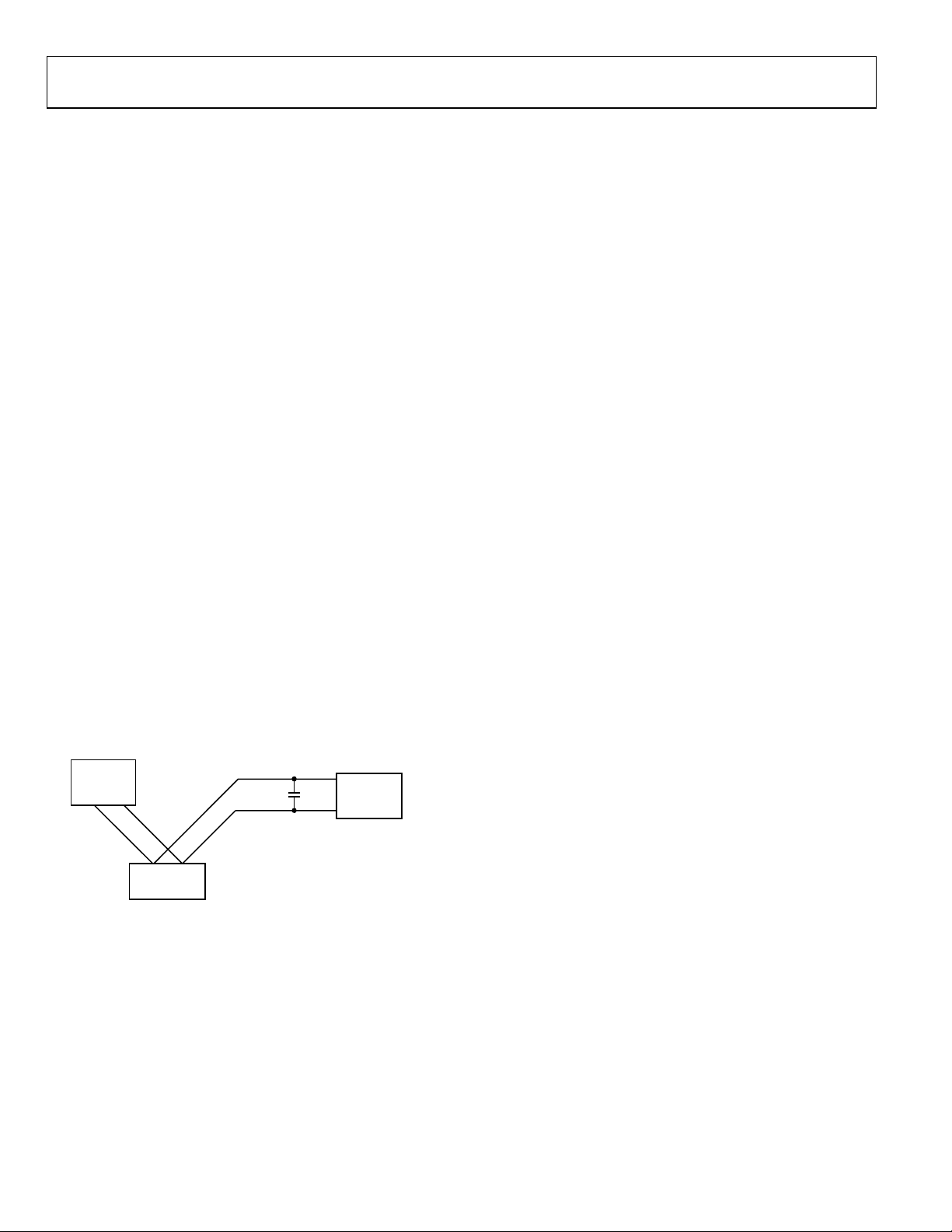
PULL-UP
SERIAL INTERFACE
MICROCONTROLLER
Figure 14. Typical SPI Interface Connection
The ADT7320 has a 4-wire serial peripheral interface (SPI). The
interface has a data input pin (DIN) for writing data to the device, a
data output pin (DOUT) for reading data back from the device,
and a serial data clock pin (SCLK) for clocking data into and out of
the device. A chip select pin (CS) enables or disables the serial
interface. CS is required for correct operation of the interface.
Data is clocked out of the ADT7320 on the falling edge of SCLK,
and data is clocked into the device on the rising edge of SCLK.
SPI COMMAND BYTE
All data transactions on the bus begin with the master taking
CS
from high to low and sending out the command byte. The
command byte indicates to the ADT7320 whether the transaction
s a read or a write and provides the address of the register for the
i
data transfer. Table 15 shows the command byte.
ADT7320
SCLK
DOUT
DIN
CS
0.1µF
TO V
DD
10kΩ10kΩ
V
GND
CT
INT
V
DD
DD
Bit C7, Bit C2, Bit C1, and Bit C0 of the command byte must all be
set to 0 to successfully begin a bus transaction. The SPI interface
does not work correctly if a 1 is written into any of these bits.
Bit C6 is the read/
write
bit; 1 indicates a read, and 0 indicates
a write.
Bits[C5:C3] contain the target register address. One register can
be read from or written to per bus transaction.
Table 15. Command Byte
C7 C6 C5 C4 C3 C2 C1 C0
0 R/W Register address 0 0 0
Rev. PrD | Page 19 of 26

ADT7320 Preliminary Technical Data
WRITING DATA
Data is written to the ADT7320 in 8 bits or 16 bits, depending on
the addressed register. The first byte written to the device is the
command byte, with the read/write bit set to 0. The master
then supplies the 8-bit or 16-bit input data on the DIN line.
The ADT7320 clocks the data into the register addressed in the
command byte on the rising edge of SCLK. The master finishes
CS
the write transaction by pulling
CS
high.
Figure 15 shows a write to an 8-bit register, and Figure 16 shows
a write to a 16-bit register.
The master must begin a new write transaction on the bus for
every register write. Only one register is written to per bus
transaction.
SCLK
DIN
1 2 3 4
8-BIT COMMAND BYTE
0
R/W REGISTER ADDR
C6
C7
5 6 7 8 9 10 11 12 13 14 15 16
8-BIT DATA
00 0
C4
C3
C1
C2C5
D5
D4 D3D7 D6
D2 D1 D0C0
09012-128
Figure 15. Writing to an 8-Bit Register
CS
SCLK
DIN
1 2 3 4
8-BIT COMMAND BYTE
0
R/W REGISTER ADDR
C7 C6 C1 D2 D1 D0C0
5246 7 8 9 10 11 12 13 14 15 16
00
C3 C2C5 C4
17
16-BIT DATA
0
D14 D13
D12 D10D11 D9 D8 D7D15
22 23
09012-129
Figure 16. Writing to a 16-Bit Register
Rev. PrD | Page 20 of 26

Preliminary Technical Data ADT7320
S
CS
CLK
DIN
DOUT
CS
SCLK
DIN
DOUT
1 2 3 4
8-BIT COMMAND BYTE
0
R/W REGISTER ADDR
C6
C7
2 3
1
8-BIT COMMAND BYTE
0
R/W REGISTER ADDR
C7 C6
5
C3
C4
0
C2C5
6
7 8
0
C1 C0
9
0
D7
D6 D5
4
Figure 17. Reading from an 8-Bit Register
5246 7 8 9 10 11 12 13 14 15 16
0
0
C4
C3
C2C5
0
C0
C1
D15
D14
D13
D12
D11
Figure 18. Reading from a 16-Bit Register
10
D10 D9
11 12
8-BIT DATA
D4
16-BIT DATA
D8 D7
13 14 15
D3 D2 D1 D0
17
16
09012-030
23
22
D1
D2
D0
09012-031
READING DATA
A read transaction begins when the master writes the command
byte to the ADT7320 with the read/write bit set to 1. The master
hen supplies 8 or 16 clock pulses, depending on the addressed
t
register, and the ADT7320 clocks out data from the addressed
register on the DOUT line. Data is clocked out on the first
falling edge of SCLK following the command byte.
The read transaction finishes when the master pulls CS high.
INTERFACING TO DSPs OR MICROCONTROLLERS
The ADT7320 can be operated with CS used as a frame
synchronization signal. This setup is useful for DSP interfaces. In
this case, the first bit (MSB) is effectively clocked out by CS
because CS normally occurs after the falling edge of SCLK in
DSPs. SCLK can continue to run between data transfers, provided
that the timing values are obeyed.
CS
can be tied to ground and the serial interface can operate in
a 3-wire mode. DIN, DOUT, and SCLK are used to communicate
with the ADT7320 in this mode.
For microcontroller interfaces, it is recommended that SCLK
idle high between data transfers.
SERIAL INTERFACE RESET
The serial interface can be reset by writing a series of 1s on the
DIN input. If a Logic 1 is written to the ADT7320 DIN line for
at least 32 serial clock cycles, the serial interface is reset. This
ensures that the interface can be reset to a known state if the
interface is lost due to a software error or a glitch in the system.
A reset returns the interface to the state in which it expects a
write to a communications register. This operation resets the
contents of all registers to their power-on values. Following a
reset, allow a period of 500 µs before addressing the serial
interface.
Rev. PrD | Page 21 of 26
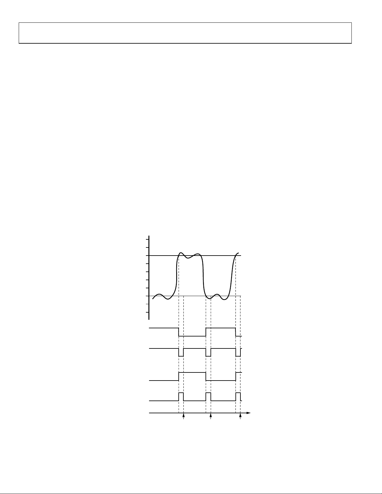
ADT7320 Preliminary Technical Data
TEMPERATURE
INT AND CT OUTPUTS
The INT and CT pins are open-drain outputs, and both pins
require a 10 kΩ pull-up resistor to VDD. The ADT7320 must be
fully powered up to VDD before reading INT and CT data.
UNDERTEMPERATURE AND OVERTEMPERATURE
DETECTION
The INT and CT pins have two undertemperature/overtemperature
modes: comparator mode and interrupt mode. The interrupt
mode is the default power-up overtemperature mode. The INT
output pin becomes active when the temperature is greater than
the temperature stored in the T
the temperature stored in the T
pin reacts after an undertemperature or overtemperature event
depends on the overtemperature mode selected.
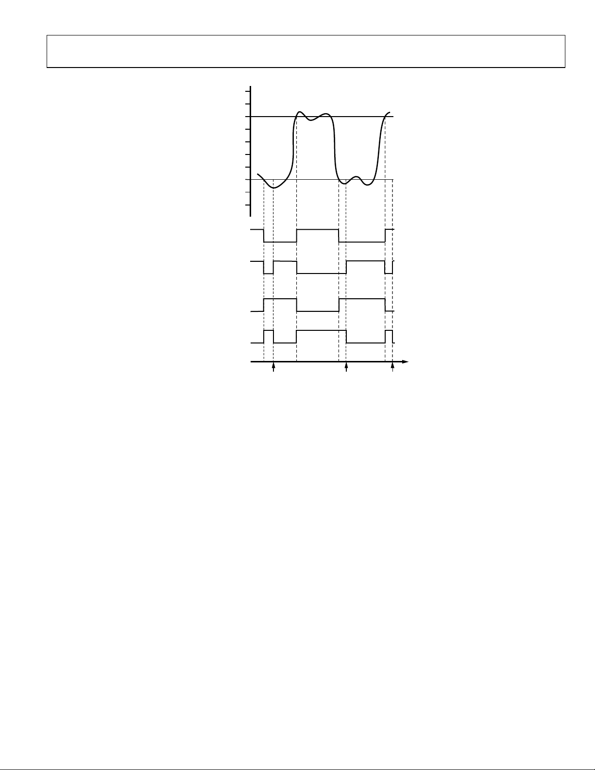
Figure 19 illustrates the comparator and interrupt modes for
events exceeding the T
limit with both pin polarity settings.
HIGH
Figure 20 illustrates the comparator and interrupt modes for
events exceeding the T
limit with both pin polarity settings.
LOW
setpoint register or less than
HIGH
setpoint register. How this
LOW
82°C
81°C
80°C
79°C
78°C
77°C
76°C
75°C
74°C
73°C
Comparator Mode
In comparator mode, the INT pin returns to its inactive status
when the temperature drops below the T
rises above the T
LOW
+ T
HYST
limit.
HIGH
− T
HYST
limit or
Placing the ADT7320 into shutdown mode does not reset the
NT state in comparator mode.
I
Interrupt Mode
In interrupt mode, the INT pin returns to its inactive status
when any ADT7320 register is read. When the INT pin is reset,
it becomes active again only when the temperature is greater
than the temperature stored in the T
than the temperature stored in the T
setpoint register or less
HIGH
setpoint register.
LOW
Placing the ADT7320 into shutdown mode resets the INT pin in
interrupt mode.
T
HIGH
T
– T
HIGH
HYST
(COMPARATOR MODE)
POLARITY = ACTIVE LOW
(INTERRUPT MODE)
POLARITY = ACTIVE LOW
(COMPARATOR MODE)
POLARITY = ACTIVE HIGH
(INTERRUPT MODE)
POLARITY = ACTIVE HIGH
INT PIN
INT PIN
INT PIN
INT PIN
Figure 19. INT Output Temperature Response for T
Rev. PrD | Page 22 of 26
READ
READ READ
Overtemperature Events
HIGH
TIME
09012-020
Preliminary Technical Data ADT7320
TEMPERATURE
–13°C
–14°C
T
–15°C
–16°C
–17°C
–18°C
–19°C
–20°C
–21°C
–22°C
+ T
LOW
HYST
T
LOW
(COMPARATOR MODE)
POLARITY = ACTIVE LOW
(INTERRUPT MODE)
POLARITY = ACTIVE LOW
(COMPARATOR MODE)
POLARITY = ACTIVE HIGH
(INTERRUPT MODE)
POLARITY = ACTIVE HIGH
Figure 20. INT Output Temperature Response for T
INT PIN
INT PIN
INT PIN
INT PIN
READ
READ READ
Undertemperature Events
LOW
TIME
09012-021
Rev. PrD | Page 23 of 26
ADT7320 Preliminary Technical Data
APPLICATIONS INFORMATION
THERMAL RESPONSE TIME
Thermal response is a function of the thermal mass of the
temperature sensor, but it is also heavily influenced by the
mass of the object that the IC is mounted to. For example, a large
PCB containing large amounts of copper tracing can act as a
large heat sink and slow the thermal response. For a faster thermal
response, it is recommended that the sensor be mounted on a
PCB that is as small as possible.
Figure 10 shows the typical response time of less than 2 seconds to
reach 63.2% of the temperature span of the DUT. The temperature
values are the digital bytes read back through the digital interface.
The response time includes all delays incurred on chip during
signal processing.
SUPPLY DECOUPLING
The ADT7320 must have a decoupling capacitor connected
etween VDD and GND; otherwise, incorrect temperature
b
readings will be obtained. A 0.1 µF decoupling capacitor, such as
a high frequency ceramic type, must be used and mounted as
close as possible to the VDD pin of the ADT7320.
If possible, the ADT7320 should be powered directly from the
system power supply. This arrangement, shown in Figure 21,
isolates the analog section from the logic switching transients.
Even if a separate power supply trace is not available, generous
supply bypassing reduces supply line induced errors. Local
supply bypassing consisting of a 0.1 µF ceramic capacitor is
critical for the temperature accuracy specifications to be
achieved.
TTL/CMOS
LOGIC
CIRCUITS
POWER
SUPPLY
Figure 21. Use of Separate Traces to Reduce Power Supply Noise
0.1µF
ADT7320
09012-022
POWERING FROM A SWITCHING REGULATOR
Precision analog devices such as the ADT7320 require a wellf
iltered power source. If the ADT7320 is powered from a switching
regulator, noise may be generated above 50 kHz that may affect
the temperature accuracy specifications. To prevent this, an RC
filter should be used between the power supply and ADT7320
. The value of the components used should be carefully
V
D
D
considered to ensure that the peak value of the supply noise is
less than 1 mV. The RC filter should be mounted as far away as
possible from the ADT7320 to ensure that the thermal mass is
kept as low as possible.
TEMPERATURE MEASUREMENT
The ADT7320 accurately measures and converts the temperature at
the surface of its own semiconductor chip. Thermal paths run
through the leads, the exposed pad, as well as the plastic package.
When the ADT7320 is used to measure the temperature of a
nearby heat source, the thermal impedance between the heat
source and the ADT7320 must be considered because this
impedance affects the accuracy and thermal response of the
measurement.
For air or surface temperature measurements, take care to isolate
the package, leads, and exposed pad from ambient air temperature.
Use of a thermally conductive adhesive can help to achieve a
more accurate surface temperature measurement.
QUICK GUIDE TO MEASURING TEMPERATURE
The following is a quick guide for measuring temperature in
continuous conversion mode (default power-up mode). Execute
each step sequentially.
1. After power-up, reset the serial interface (load 32
consecutive 1s on DIN). This ensures all internal circuitry
is properly initialized.
2. Verify the setup by reading the device ID
(Register Address 0x03). It should read 0xC3.
3. After consistent consecutive readings are obtained from
Step 2, read the configuration register (Register Address 0x01),
T
(Register Address 0x04), T
CRIT
and T
(Register Address 0x07). Compare these values
LOW
with the specified defaults in Table 6. If all the readings
match, the interface is operational.
4. Write to the configuration register to set the ADT7320 to
he desired configuration. Read the temperature value register.
t
It should produce a valid temperature measurement.
(Register Address 0x06),
HIGH
Rev. PrD | Page 24 of 26
Preliminary Technical Data ADT7320
4.1
0
S
I
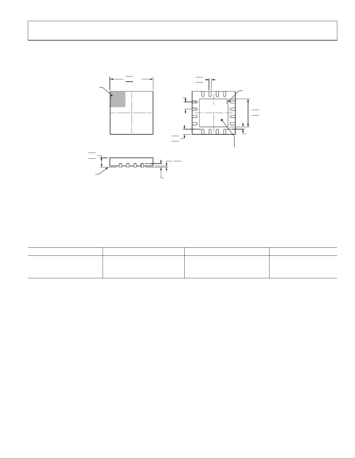
OUTLINE DIMENSIONS
0.35
0.30
0.25
13
12
9
8
BOTTOM VIEWTOP VIEW
COPLANARITY
0.08
P
I
N
1
N
I
D
C
I
16
EXPOSED
1
PAD
4
5
FOR PROPER CONNECTION OF
THE EXPOSED PAD, REFER TO
THE PIN CONFIGURATION AND
FUNCTION DESCRIPTIONS
SECTION OF THIS DATA SHEET.
A
2.70
2.60 SQ
2.50
0.20 MIN
O
R
T
08-16-2010-C
PIN 1
NDICATOR
0.80
0.75
0.70
EATING
PLANE
4.00 SQ
3.90
0.65
BSC
0.45
0.40
0.35
0.05 MAX
0.02 NOM
0.20 REF
COMPLIANTTOJEDEC STANDARDS MO-220-WGGC.
Figure 22. 16-Lead Lead Frame Chip Scale Package [LFCSP_WQ]
4 mm × 4 mm Body, Very Very Thin Quad
(CP-16-17)
Dimensions shown in millimeters
ORDERING GUIDE
Model1 Temperature Range2 Package Description Package Option
ADT7320UCPZ-R2 −40°C to +150°C 16-lead LFCSP_WQ CP-16-17
ADT7320UCPZ-RL7 −40°C to +150°C 16-Lead LFCSP_WQ CP-16-17
EVAL-ADT7X20EBZ Evaluation Board
1
Z = RoHS Compliant Part.
2
Operating at extended temperatures over prolonged periods may shorten the lifetime performance of the part.
Rev. PrD | Page 25 of 26

ADT7320 Pr
NOTES
eliminary Technical Data
©2011 Analog Devices, Inc. All ri ghts reserved. Trademarks and
registered trademarks are the property of their respective owners.
PR0
9012-0-11/11(PrD)
R
ev. PrD | Page 26 of 26
 Loading...