Automotive, ±0.5°C Accurate, 16-Bit
Data Sheet
FEATURES
Qualified for automotive applications
High performance
Temperature accuracy
±0.5°C from −40°C to +105°C (2.7 V to 3.6 V)
±0.4°C from −40°C to +105°C (3.0 V)
16-bit temperature resolution: 0.0078°C
Fast first conversion on power-up of 6 ms
Easy implementation
No temperature calibration/correction required by user
No linearity correction required
Low power
Power saving 1 sample per second (SPS) mode
700 μW typical at 3.3 V in normal mode
7 μW typical at 3.3 V in shutdown mode
Wide operating ranges
Temperature range: −40°C to +150°C
Voltage range: 2.7 V to 5.5 V
Programmable interrupts
Critical overtemperature interrupt
Overtemperature/undertemperature interrupt
SPI-compatible interface
8-lead narrow SOIC RoHS-compliant package
APPLICATIONS
Battery management
Climate control and infotainment
Lighting
Power train
Thermocouple cold junction compensation
GPS
Digital SPI Temperature Sensor
ADT7311
GENERAL DESCRIPTION
The ADT7311 is a high accuracy digital temperature sensor
in a narrow 8-lead SOIC package. It contains a band gap
temperature reference and a 16-bit ADC to monitor and digitize
the temperature to a 0.0078°C resolution. The ADC resolution,
by default, is set to 13 bits (0.0625°C). The ADC resolution is a
user programmable mode that can be changed through the
serial interface.
The ADT7311 is guaranteed to operate over supply voltages from
2.7 V to 5.5 V. Operating at 3.3 V, the average supply current is
typically 210 A. The ADT7311 has a shutdown mode that
powers down the device and offers a shutdown current of
typically 2 A. The ADT7311 is rated for operation over the
−40°C to +150°C temperature range.
The CT pin is an open-drain output that becomes active when
the temperature exceeds a programmable critical temperature
limit. The default critical temperature limit is 147°C. The INT
pin is also an open-drain output that becomes active when the
temperature exceeds a programmable limit. The INT and CT
pins can operate in either comparator or interrupt mode.
PRODUCT HIGHLIGHTS
1. Ease of use, no calibration or correction required by the user.
2. Low power consumption.
3. Excellent long-term stability and reliability.
4. Packaged in an 8-lead SOIC, RoHS-compliant package.
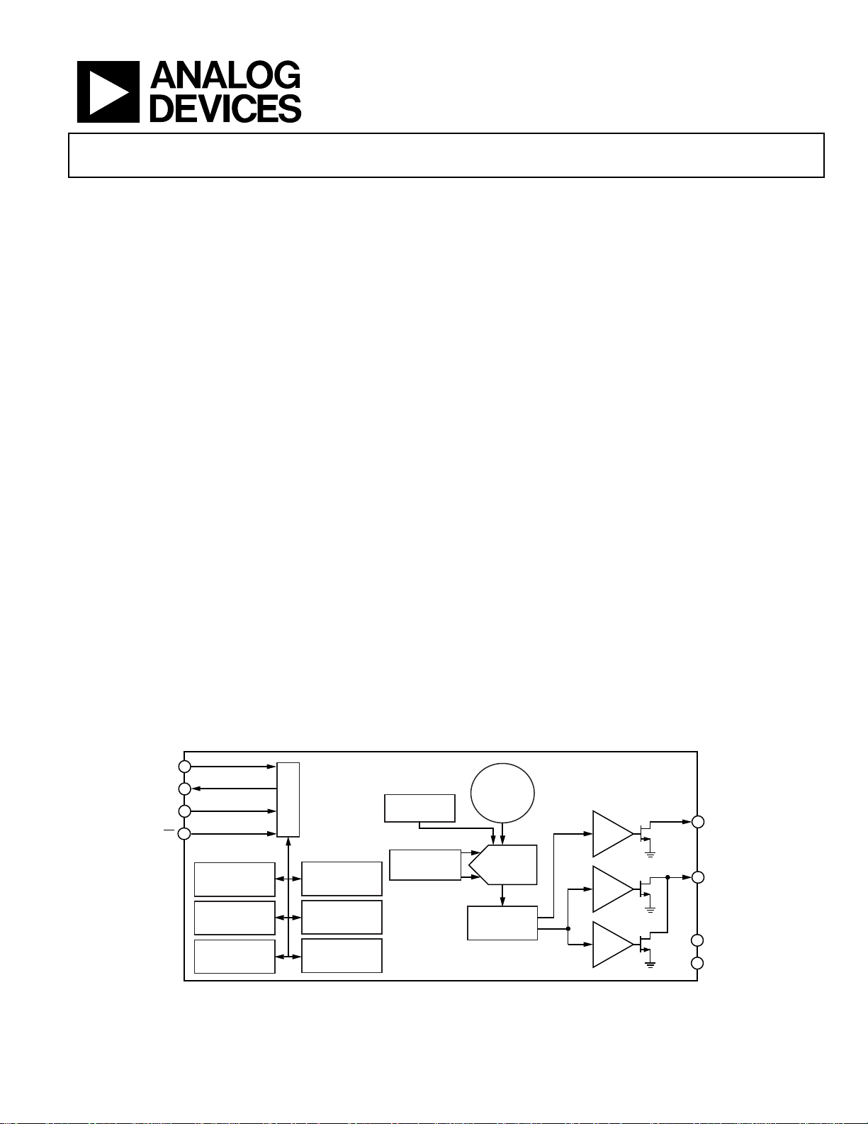
FUNCTIONAL BLOCK DIAGRAM
1
SCLK
2
DOUT
3
DIN
4
CS
TEMPERATURE
VALUE
REGISTER
T
HYST
REGISTER
T
HIGH
REGISTER
Rev. 0
Information furnished by Analog Devices is believed to be accurate and reliable. However, no
responsibility is assumed by Anal og Devices for its use, nor for any infringements of patents or ot her
rights of third parties that may result from its use. Specifications subject to change without notice. No
license is granted by implication or otherwise under any patent or patent rights of Analog Devices.
Trademarks and registered trademarks are the property of their respective owners.
SPI I NTERFACE
CONFIGURATION,
STATUS, AND
ID REGISTERS
T
CRIT
REGISTER
T
LOW
REGISTER
INTERNAL
REFERENCE
TEMPERATURE
SENSOR
ADT7311
INTERNAL
OSCILLATOR
6
CT
5
INT
7
GND
V
8
DD
Σ-∆
MODULATOR
FILTER
LOGIC
T
T
T
CRIT
HIGH
LOW
Figure 1.
One Technology Way, P.O. Box 9106, Norwood, MA 02062-9106, U.S.A.
Tel: 781.329.4700 www.analog.com
Fax: 781.461.3113 ©2011 Analog Devices, Inc. All rights reserved.
9050-001

ADT7311 Data Sheet
TABLE OF CONTENTS
Features.............................................................................................. 1
Configuration Register .............................................................. 14
Applications....................................................................................... 1
General Description ......................................................................... 1
Product Highlights ........................................................................... 1
Functional Block Diagram .............................................................. 1
Revision History ............................................................................... 2
Specifications..................................................................................... 3
SPI Timing Specifications ........................................................... 4
Absolute Maximum Ratings............................................................ 5
ESD Caution.................................................................................. 5
Pin Configuration and Function Descriptions............................. 6
Typical Performance Characteristics ............................................. 7
Theory of Operation ........................................................................ 9
Circuit Information...................................................................... 9
Converter Details.......................................................................... 9
Temperature Measurement......................................................... 9
Temperature Value Register ...................................................... 15
ID Register................................................................................... 15
T
Setpoint Register ............................................................... 15
CRIT
T
Setpoint Register............................................................... 16
HYST
T
Setpoint Register .............................................................. 16
HIGH
T
Setpoint Register ............................................................... 16
LOW
Serial Peripheral Interface............................................................. 17
SPI Command Byte.................................................................... 17
Writing Data ............................................................................... 18
Reading Data............................................................................... 19
Interfacing to DSPs or Microcontrollers................................. 19
Serial Interface Reset.................................................................. 19
INT and CT Outputs...................................................................... 20
Undertemperature and Overtemperature Detection ............ 20
Applications Information.............................................................. 22
One-Shot Mode ..........................................................................10
1 SPS Mode.................................................................................. 10
Shutdown..................................................................................... 11
Fault Queue................................................................................. 11
Temperature Data Format......................................................... 12
Temperature Conversion Formulas .........................................12
Registers........................................................................................... 13
Status Register............................................................................. 13
REVISION HISTORY
9/11—Revision 0: Initial Version
Thermal Response Time ........................................................... 22
Supply Decoupling..................................................................... 22
Powering from a Switching Regulator..................................... 22
Temperature Monitoring........................................................... 22
Quick Guide to Measuring Temperature ................................ 22
Outline Dimensions....................................................................... 23
Ordering Guide .......................................................................... 23
Automotive Products................................................................. 23
Rev. 0 | Page 2 of 24

Data Sheet ADT7311
SPECIFICATIONS
TA = −40°C to +150°C; VDD = 2.7 V to 5.5 V; unless otherwise noted.
Table 1.
Parameter Min Typ Max Unit Test Conditions/Comments
TEMPERATURE SENSOR AND ADC
Accuracy1 −0.05 ±0.4 °C TA = −40°C to +105°C, VDD = 3.0 V
±0.44 °C TA = −40°C to +105°C, VDD = 2.7 V to 3.3 V
±0.5 °C TA = −40°C to +125°C, VDD = 3.0 V
±0.5 °C TA = −40°C to +105°C, VDD = 2.7 V to 3.6 V
±0.7 °C TA = −40°C to +150°C, VDD = 2.7 V to 3.6 V
±0.8 °C TA = −40°C to +105°C, VDD = 4.5 V to 5.5 V
±1.0 °C TA = −40°C to +150°C, VDD = 2.7 V to 5.5 V
ADC Resolution 13 Bits
16 Bits
Temperature Resolution
13-Bit 0.0625 °C 13-bit resolution (sign + 12 bits)
16-Bit 0.0078 °C 16-bit resolution (sign + 15 bits)
Temperature Conversion Time 240 ms Continuous conversion and one-shot conversion mode
Fast Temperature Conversion Time 6 ms First conversion on power-up only
1 SPS Conversion Time 60 ms Conversion time for 1 SPS mode
Temperature Hysteresis ±0.002 °C Temperature cycle = 25°C to 125°C and back to 25°C
Repeatability ±0.015 °C TA = 25°C
DC PSRR 0.1 °C/V TA = 25°C
DIGITAL OUTPUTS (CT, INT), OPEN
DRAIN
High Output Leakage Current, IOH 0.1 5 μA CT and INT pins pulled up to 5.5 V
Output Low Voltage, VOL 0.4 V IOL = 2 mA at 5.5 V, IOL = 1 mA at 3.3 V
Output High Voltage, VOH
0.7 ×
V
VDD
Output Capacitance, C
OUT
DIGITAL INPUTS (DIN, SCLK, CS)
2 pF
Input Current ±1 μA VIN = 0 V to VDD
Input Low Voltage, VIL 0.4 V
Input High Voltage, VIH
0.7 ×
V
DD
V
Pin Capacitance 5 10 pF
DIGITAL OUTPUT (DOUT)
Output High Voltage, VOH
V
OH
V I
−
0.3
Output Low Voltage, V
Output Capacitance, C
OL
50 pF
OUT
0.4 V IOL = 200 μA
POWER REQUIREMENTS
Supply Voltage 2.7 5.5 V
Supply Current
At 3.3 V 210 265 μA Peak current while converting, SPI interface inactive
At 5.5 V 250 300 μA Peak current while converting, SPI interface inactive
1 SPS Current
At 3.3 V 46 μA VDD = 3.3 V, 1 SPS mode, TA = 25°C
At 5.5 V 65 μA VDD = 5.5 V, 1 SPS mode, TA = 25°C
Twos complement temperature value of sign bit plus
12 ADC bits (power-up default resolution)
Twos complement temperature value of sign bit plus
15 ADC bits (Bit 7 = 1 in the configuration register)
= I
SOURCE
= 200 μA
SINK
Rev. 0 | Page 3 of 24
ADT7311 Data Sheet
Parameter Min Typ Max Unit Test Conditions/Comments
Shutdown Current
At 3.3 V 2.0 15 μA Supply current in shutdown mode
At 5.5 V 5.2 25 μA Supply current in shutdown mode
Power Dissipation Normal Mode 700 μW VDD = 3.3 V, normal mode at 25°C
Power Dissipation 1 SPS 150 μW Power dissipated for VDD = 3.3 V, TA = 25°C
1
Accuracy includes lifetime drift.
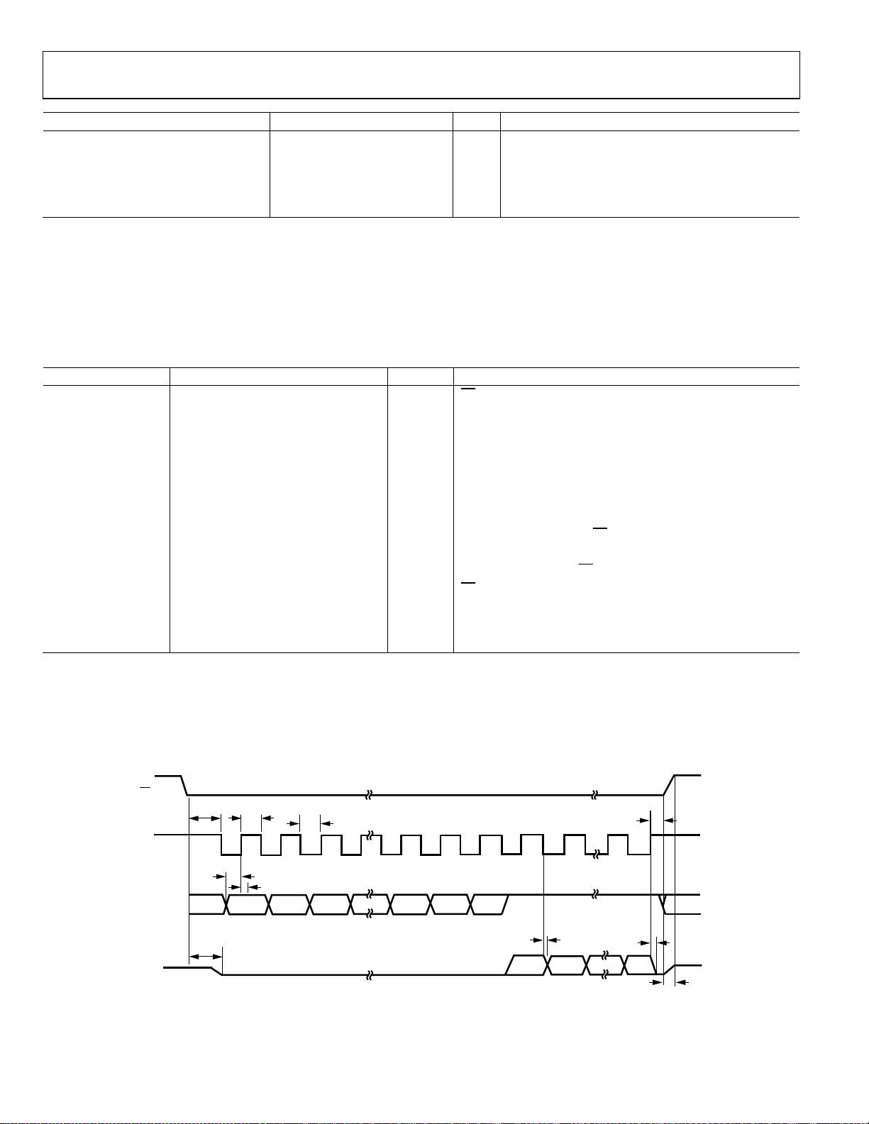
SPI TIMING SPECIFICATIONS
TA = −40°C to +150°C, VDD = 2.7 V to 5.5 V, unless otherwise noted. All input signals are specified with rise time (tR) = fall time (tF) = 5 ns
(10% to 90% of V
) and timed from a voltage level of 1.6 V.
DD
Table 2.
Parameter
t1 0 ns min
1, 2
Limit at T
MIN
, T
Unit Conditions/Comments
MAX
falling edge to SCLK active edge setup time
CS
t2 100 ns min SCLK high pulse width
t3 100 ns min SCLK low pulse width
t4 30 ns min Data setup time prior to SCLK rising edge
t5 25 ns min Data hold time after SCLK rising edge
t6 5 ns min Data access time after SCLK falling edge
60 ns max VDD = 4.5 V to 5.5 V
80 ns max VDD = 2.7 V to 3.6 V
3
t
10 ns min
7
Bus relinquish time after CS
inactive edge
80 ns max
t8 0 ns min
t9 0 ns min
SCLK inactive edge to CS
falling edge to DOUT active time
CS
rising edge hold time
60 ns max VDD = 4.5 V to 5.5 V
80 ns max VDD = 2.7 V to 3.6 V
t10 10 ns min SCLK inactive edge to DOUT low
1
Sample tested during initial release to ensure compliance. All input signals are specified with tR = tF = 5 ns (10% to 90% of VDD) and timed from a voltage level of 1.6 V.
2
See Figure 2.
3
This means that the times quoted in the timing characteristics in Table 2 are the true bus relinquish times of the part and, as such, are independent of external bus
loading capacitances.
CS
SCLK
DIN
DOUT
t
1
t
2
1
t
4
t
MSB LSB
t
9
t
3
23
5
Figure 2. Detailed SPI Timing Diagram
Rev. 0 | Page 4 of 24
t
8
9102324
8
76
t
6
MSB
t
10
LSB
t
7
09050-002
Data Sheet ADT7311
ABSOLUTE MAXIMUM RATINGS
Table 3.
Parameter Rating
VDD to GND −0.3 V to +7 V
DIN Input Voltage to GND −0.3 V to VDD + 0.3 V
DOUT Voltage to GND −0.3 V to VDD + 0.3 V
SCLK Input Voltage to GND −0.3 V to VDD + 0.3 V
CS Input Voltage to GND
−0.3 V to V
+ 0.3 V
DD
CT and INT Output Voltage to GND −0.3 V to VDD + 0.3 V
ESD Rating (Human Body Model) 2.0 kV
Operating Temperature Range1 −40°C to +150°C
Storage Temperature Range −65°C to +160°C
Maximum Junction Temperature, T
150°C
JMAX
8-Lead SOIC_N (R-8)
Power Dissipation2 W
MAX
= (T
JMAX
− T
A
3
)/θJA
Thermal Impedance4
θJA, Junction-to-Ambient (Still Air) 121°C/W
θJC, Junction-to-Case 56°C/W
IR Reflow Soldering 220°C
Peak Temperature (RoHS-Compliant
260°C (0°C)
Package)
Time at Peak Temperature 20 sec to 40 sec
Ramp-Up Rate 3°C/sec maximum
Ramp-Down Rate −6°C/sec maximum
Time from 25°C to Peak Temperature 8 minutes maximum
1
Operating at extended temperatures over prolonged periods depends on
the lifetime performance of the part. Consult your local Analog Devices, Inc.,
account representative for more details.
2
Value relates to package being used on a standard 2-layer PCB. This gives a
worst-case θJA and θJC.
3
TA = ambient temperature.
4
Junction-to-case resistance is applicable to components featuring a
preferential flow direction, for example, components mounted on a heat
sink. Junction-to-ambient is more useful for air-cooled, PCB-mounted
components.
Stresses above those listed under Absolute Maximum Ratings
may cause permanent damage to the device. This is a stress
rating only; functional operation of the device at these or any
other conditions above those indicated in the operational
section of this specification is not implied. Exposure to absolute
maximum rating conditions for extended periods may affect
device reliability.
ESD CAUTION
Rev. 0 | Page 5 of 24

ADT7311 Data Sheet
PIN CONFIGURATION AND FUNCTION DESCRIPTIONS
SCLK
1
ADT7311
2
DOUT
3
DIN
TOP VIEW
(Not to Scale)
CS
4
Figure 3. Pin Configuration
Table 4. Pin Function Descriptions
Pin No. Mnemonic Description
1 SCLK Serial Clock Input. The serial clock is used to clock in and clock out data to and from any register of the ADT7311.
2 DOUT Serial Data Output. Data is clocked out on the SCLK falling edge and is valid on the SCLK rising edge.
3 DIN
Serial Data Input. Serial data to be loaded to the part’s control registers is provided on this input. Data is clocked
into the registers on the rising edge of SCLK.
4
CS
5 INT
Chip Select Input. The device is selected when this input is low. The device is disabled when this pin is high.
Overtemperature and Undertemperature Indicator. Logic output. The power-up default setting is as an active
low comparator interrupt. Open-drain configuration. A pull-up resistor is required, typically 10 kΩ.
6 CT
Critical Overtemperature Indicator. Logic output. Power-up default polarity is active low. Open-drain
configuration. A pull-up resistor is required, typically 10 kΩ.
7 GND Analog and Digital Ground.
8 VDD Positive Supply Voltage (2.7 V to 5.5 V). The supply should be decoupled with a 0.1 μF ceramic capacitor to GND.
V
8
DD
7
GND
6
CT
INT
5
09050-005
Rev. 0 | Page 6 of 24
Data Sheet ADT7311
A
A
TYPICAL PERFORMANCE CHARACTERISTICS
1.0
0.8
0.6
0.4
0.2
0
TURE ERROR (°C)
–0.2
–0.4
TEMPER
–0.6
–0.8
–1.0
–60 –40 –20 0 20 40 60 80 100 120 140 160
MAX ACCURACY LIMITS
MAX ACCURACY LIMITS
TEMPERATURE (°C)
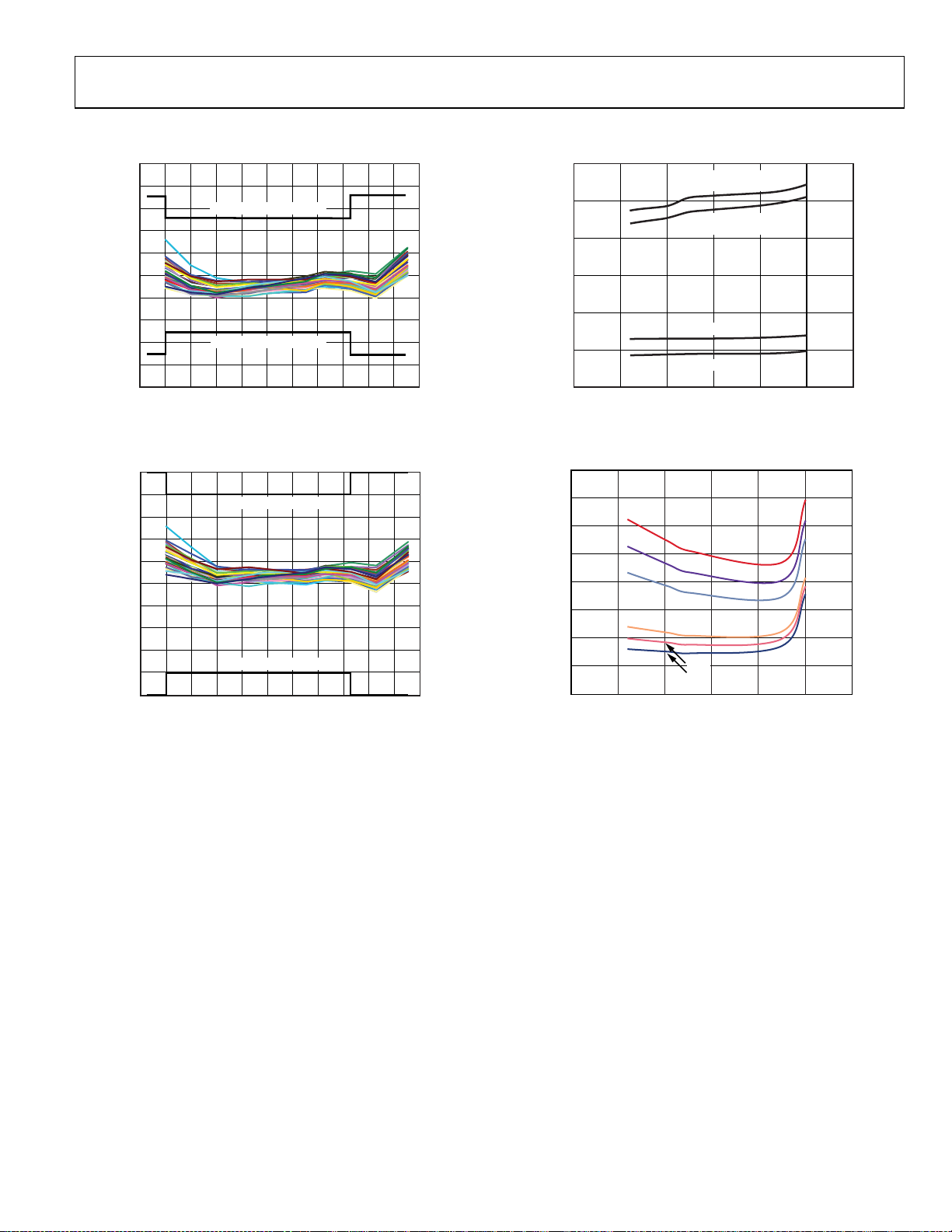
Figure 4. Temperature Accuracy at 3 V
09050-006
300
250
200
(µA)
150
DD
I
100
50
0
–100 –50 0 50 100 150 200
5.5V CONTI NUOUS
CONVERSION
3.0V CONTI NUOUS
CONVERSIO N
5.5V 1SPS
3.0V 1SPS
TEMPERATURE (°C)
Figure 6. Operating Supply Current vs. Temperature
9050-007
1.0
0.8
0.6
0.4
0.2
0
TURE ERROR (° C)
–0.2
–0.4
TEMPER
–0.6
–0.8
–1.0
–60 –40 –20 0 20 40 60 80 100 120 140 160
MAX ACCURACY LIMI TS
MAX ACCURACY LIMI TS
TEMPERATURE (°C)
Figure 5. Temperature Accuracy at 5 V
8
7
6
5
4
(µA)
DD
I
3
2
1
0
–100 –50 0 50 100 150 200
09050-024
5.5V
5.0V
4.5V
3.6V
3.0V
2.7V
TEMPERATURE (°C)
09050-025
Figure 7. Shutdown Current vs. Temperature
Rev. 0 | Page 7 of 24
ADT7311 Data Sheet
(
300
160
250
200
µA)
150
DD
I
100
50
0
2.53.03.54.04.55.05.56.0
IDD CONTINUOUS CONVERSIO N
I
1SPS
DD
SUPPLY VOLTAGE (V)
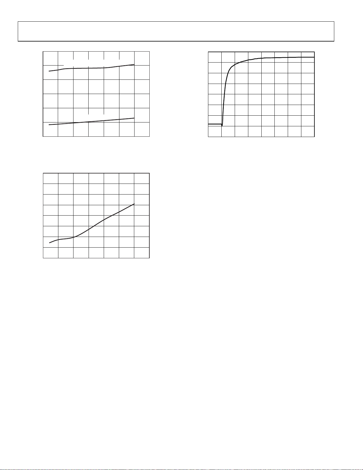
Figure 8. Average Operating Supply Current vs. Supply Voltage at 25°C
8
7
6
(µA)
5
DD
4
3
SHUTDOWN I
2
140
120
100
80
60
TEMPERATURE (° C)
40
20
0
043530252015105
09050-008
TIME (Seconds)
0
09050-011
Figure 10. Response to Thermal Shock
1
0
2.53.03.54.04.55.05.56.0
SUPPLY VOLTAGE (V)
9050-009
Figure 9. Shutdown Current vs. Supply Voltage at 25°C
Rev. 0 | Page 8 of 24
 Loading...