

GND
13-Bit, ±0.5°C Accurate, MicroPower Digital
Temperature Sensor in 6-Lead SOT-23
Preliminary Technical Data
FEATURES
13-bit temperature-to-digital converter
−40°C to +150°C operating temperature range
±0.5°C typical accuracy
0.03125°C temperature resolution
Shutdown current of 1 µA
Power dissipation of 0.631 mW at V
SPI- and DSP-compatible serial interface
Shutdown mode
Space-saving SOT-23 and MSOP packages
APPLICATIONS
Medical equipment
Automotive:
Environmental controls
Oil temperature
Hydraulic systems
Cell phones
Hard disk drives
Personal computers
Electronic test equipment
Office equipment
Domestic appliances
Process control
GENERAL DESCRIPTION
The ADT7301 is a complete temperature monitoring system
available in SOT-23 and MSOP packages. It contains a band gap
temperature sensor and a 13-bit ADC to monitor and digitize
the temperature reading to a resolution of 0.03125°C.
The ADT7301 has a flexible serial interface that allows easy
interfacing to most microcontrollers. The interface is compatible with SPI®, QSPI™, and MICROWIRE™ protocols as well as
DSPs. The part features a standby mode that is controlled via
the serial interface. The ADT7301’s wide supply voltage range,
low supply current, and SPI compatible interface make it ideal
for a variety of applications, including personal computers,
office equipment, automotive, and domestic appliances. The
ADT7301 is rated for operation over the -40°C to +150°C
temperature range. It is not recommended to operate the device
at temperatures above +125°C for greater than a total of 5%
(5,000 hours) of the lifetime of the device. Any exposure
beyond this limit will affect device reliability.
= 3.3 V
DD
ADT7301
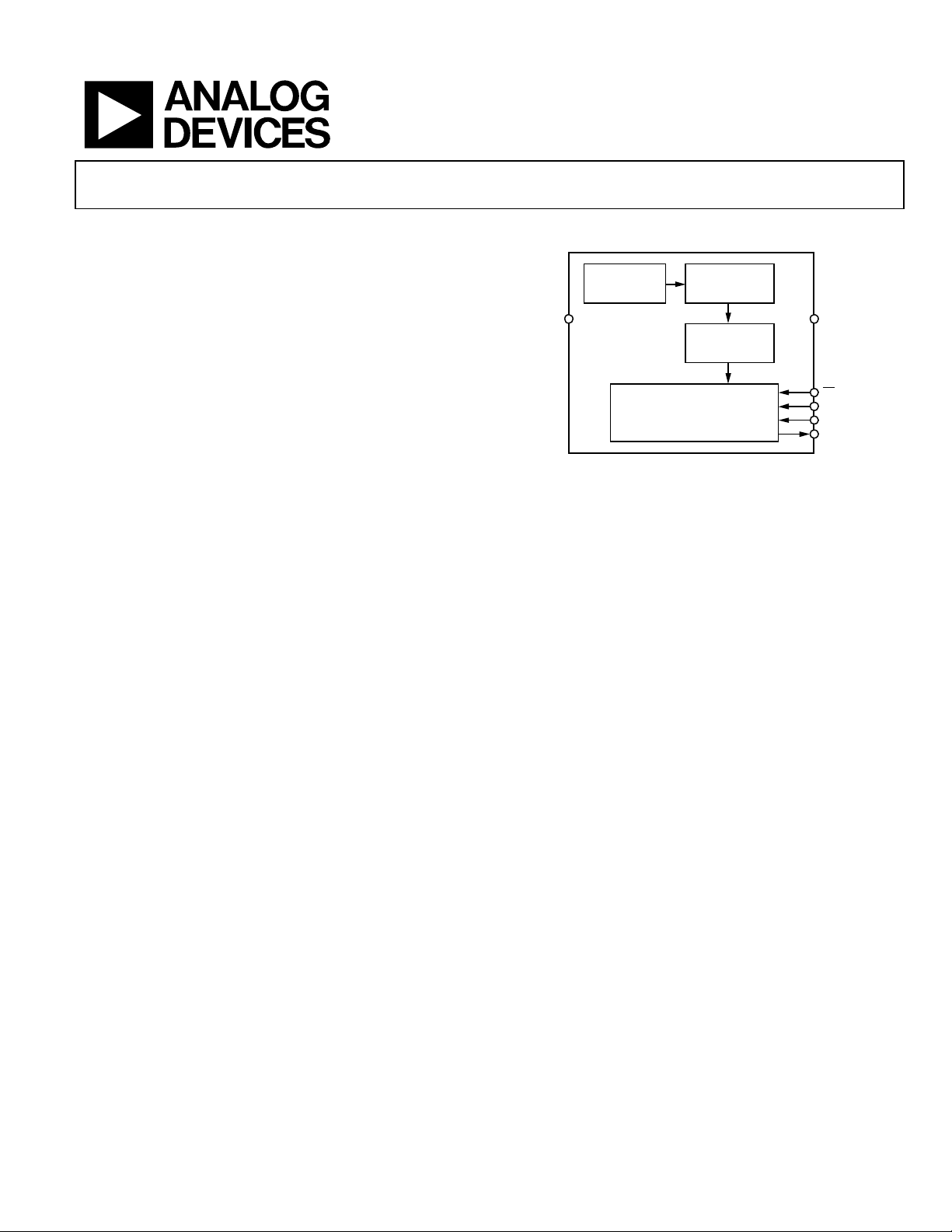
FUNCTIONAL BLOCK DIAGRAM
BAND GAP
TEMPERATURE
SENSOR
ADT7301
INTERFACE
Figure 1. Functional Bloc k Diagram
PRODUCT HIGHLIGHTS
1. The ADT7301 has an on-chip temperature sensor that
allows an accurate measurement of the ambient temperature. The measurable temperature range is −40°C to
+150°C.
2. Supply voltage of 2.7 V to 5.5 V.
3. Space-saving 6-lead SOT-23 and 8-lead MSOP packages.
4. Temperature accuracy of ±0.5°C.
5. 13-bit temperature reading to 0.03125°C resolution.
6. The ADT7301 features a shutdown mode that reduces the
power consumption to 4.88 µW with VDD = 3.3 V @ 1 SPS.
13-BIT
ANALOG/DIGITAL
CONVERTER
TEMPERATURE
VALUE
REGISTER
SERIAL
BUS
V
DD
CS
SCLK
DIN
DOUT
02884-0-001
Rev. PrJ
Information fu rnished by Analog Devices is believed to be accu rate and re liable.
However, no responsibility is assumed by Analog Devices for its use, nor for any
infringements of patents or other rights of third parties that may result from its use.
Specifications subject to change without notice. No license is granted by implication
or otherwise under any patent or patent rights of Analog Devices. Trademarks and
registered tr ademarks are th e property of th eir respective o wners.
One Technology Way, P.O. Box 9106, Norwood, MA 02062-9106, U.S. A.
Tel: 781.329.4 700
Fax: 781.326.8703
www.analog.com
© 2004 Analog Devices, Inc. All rights re served.

ADT7301
Rev. PrJ | Page 2 of 14
TABLE OF CONTENTS
Specifications..................................................................................... 3
Preliminary Technical Data
Temperature Value Register........................................................ 8
Timing Characteristics.................................................................4
Absolute Maximum Ratings............................................................5
ESD Caution.................................................................................. 5
Pin Configurations and Function Descriptions............................6
Typical Performance Characteristics..............................................7
Circuit Information ..........................................................................8
Converter Details..........................................................................8
REVISION HISTORY
Revision PrE: Preliminary Version
Serial Interface .............................................................................. 9
Microprocessor Interfacing....................................................... 10
Mounting The ADT7302........................................................... 12
Supply Decoupling ..................................................................... 12
Outline Dimensions....................................................................... 13
Ordering Guide............................................................................... 14

Preliminary Technical Data ADT7301
Rev. PrJ | Page 3 of 14
SPECIFICATIONS
TA = T
Table 1. A Grade Specifications
Parameter Min Typ Max Unit Test Conditions/Comments
TEMPERATURE SENSOR AND ADC VDD = +3.3 V (±10%) and 5 V (±10%)
TBD ±2 °C TA = −20°C to +85°C.
TBD ±3 °C TA = −40°C to +125°C.
TBD ±41 °C TA = −40°C to +150°C.
SUPPLIES
190 300 µA VDD = 3.3 V. Powered up and not converting
1.6 2.2 mA VDD = 5 V. Powered up and converting
280 400 µA VDD = 5 V. Powered up and not converting
0.2 1 µA VDD = 5 V.
7.4 µW VDD = 5 V
65 µW VDD = 5 V
641 µW VDD = 5 V
DIGITAL INPUT4
DIGITAL OUTPUT5
1
It is not recommended to operate the device at temperatures above +125°C for greater than a total of 5% (5,000 hours) of the lifetime of the device. Any exposure
beyond this limit will affect device reliability.
2
Thermal Time Constant is the time it takes for a starting temperature difference to change to 36.8% of it’s starting value. For example if the ADT7301 experienced a
thermal shock from 0°C to 100°C, it would take typically 2 secs for the ADT7301 to reach 63.2°C.
3
The ADT7301 is taken out of shutdown mode and a temperature conversion is immediately performed after this write operation. Once the temperature conversion is
complete the ADT7301 is put back into shutdown mode.
4
Guaranteed by design and characterization, not production tested.
5
Guaranteed by design and characterization, not production tested.
Specifications subject to change without notice
to T
MIN
, VDD = 2.7 V to 5.5 V, unless otherwise noted. All specifications apply for –40°C to +150°C, unless otherwise stated
MAX
Accuracy TBD ±1 °C TA = 0°C to 70°C.
Temperature Resolution 0.03125 °C
Auto Conversion Update Rate, tR 1 sec Temperature measurement every 1 second
Temperature Conversion Time 2 ms
Thermal Time Constant2 2 sec
Supply Voltage 2.7 5.5 V For Specified Performance
Supply Current
Normal Mode 1.6 2.2 mA VDD = 3.3 V. Powered up and converting
Shutdown Mode 0.2 1 µA VDD = 3.3 V.
Power Dissipation
Normal Mode (Average) 631 µW VDD = 3.3 V. Auto conversion update, tR.
1.41 mW VDD = +5 V. Auto conversion update, tR.
Shutdown Mode (Average)3
1 sps 4.88 µW VDD = 3.3 V
10 sps 42.9 µW VDD = 3.3 V
100 sps 423 µW VDD = 3.3 V
Input High Voltage, VIH 2.5 V
Input Low Voltage, VIL 0.8 V
Input Current, IIN ±1 µA VIN = 0 V to VDD
Input Capacitance, CIN 10 pF All digital inputs
Output High Voltage, VOH V
− 0.3 V I
DD
SOURCE
= I
= 200 µA
SINK
Output Low Voltage, VOL 0.4 V IOL = 200 µA
Output Capacitance, C
50 pF
OUT
ADT7301 Preliminary Technical Data
TIMING CHARACTERISTICS
Guaranteed by design and characterization, not production tested. All input signals are specified with tr = tf = 5 ns (10% to 90% of VDD)
and timed from a voltage level of 1.6 V.
= T
to T
T
A
MIN
Table 2.
Param eter1 Limit Unit Comments
t1 5 ns min
t2 25 ns min SCLK High Pulse Width
t3 25 ns min SCLK Low Pulse Width
t4 2 35 ns max Data Access Time after SCLK Falling Edge
t
5
t6 5 ns min Data Hold Time after SCLK Rising Edge
t7 5 ns min
2
t
40 ns max
8
1
See Figure 13. for SPI Timing diagram.
2
Measured with the load circuit of Figure 2
, VDD = 2.7 V to 5.5 V, unless otherwise noted.
MAX
20 ns min Data Setup Time prior to SCLK Rising Edge
200µA
CS
to SCLK Setup Time
CS
to SCLK Hold Time
CS
to DOUT High Impedance
I
OL
TO
OUTPUT
PIN
50pF
C
L
200µAI
OH
1.6V
02884-0-002
Figure 2. Load Circ uit for Dat a Access Time and Bus Relinquish Time
Rev. PrJ | Page 4 of 14
Preliminary Technical Data ADT7301
ABSOLUTE MAXIMUM RATINGS
Table 3. ADT7301 Stress Ratings
Parameter Rating
VDD to GND −0.3 V to +7 V
Digital Input Voltage to GND −0.3 V to VDD + 0.3 V
Digital Output Voltage to GND −0.3 V to VDD + 0.3 V
Operating Temperature Range1 −40°C to +150°C
Storage Temperature Range −65°C to +150°C
Junction Temperature +150°C
6-Lead SOT-23 (RJ-6)
Power Dissipation2 W
MAX
= (T
JMAX
- T
3
A
)/θJA
Thermal Impedance
θJA, Junction-to-Ambient (still air) 190.4°C/W
8-Lead MSOP (RM-8)
Power Dissipation2 W
MAX
= (T
JMAX
- T
3)
/θJA
A
Thermal Impedance4
θJA, Junction-to-Ambient (still air) 205.9°C/W
θJC, Junction-to-Case 43.74°C/W
IR Reflow Soldering
Peak Temperature +220°C (−0/+5°C)
Time at Peak Temperature 10 s to 20 s
Ramp-up Rate 2°C/s to 3°C/s
Ramp-down Rate −6°C/sec
1
It is not recommended to operate the ADT7301 at temperatures above 125°C
for greater than a total of 5% of the lifetime of the device. Any exposure
beyond this limit will affect device reliability.
2
Values relate to package being used on a standard 2-layer PCB. Reference
Figure 3 for a plot of maximum power dissipation versus ambient
temperature (T
3
TA = ambient temperature
4
Junction-to-case resistance is applicable to components featuring a
preferential flow direction, e.g., components mounted on a heat sink.
Junction-to-ambient resistance is more useful for air- cooled, PCB mounted
components.
).
A
Stresses above those listed under Absolute Maximum Ratings
may cause permanent damage to the device. This is a stress
rating only; functional operation of the device at these or any
other conditions above those indicated in the operational
section of this specification is not implied. Exposure to absolute
maximum rating conditions for extended periods may affect
device reliability
1.2
1.0
0.8
0.6
0.4
0.2
MAXIMUM POWER DISSIPATION (W)
0
–10
–20
–30
–40
0
Figure 3. Plot of Maximum Power Dissipation vs. Temperature
SOT-23
MSOP
50
40
30
20
10
TEMPERATURE (°C)
150
140
130
120
110
100
90
80
70
60
02884-0-003
ESD CAUTION
ESD (electrostatic discharge) sensitive device. Electrostatic charges as high as 4000 V readily accumulate on the
human body and test equipment and can discharge without detection. Although this product features
proprietary ESD protection circuitry, permanent damage may occur on devices subjected to high energy
electrostatic discharges. Therefore, proper ESD precautions are recommended to avoid performance
degradation or loss of functionality.
Rev. PrJ | Page 5 of 14

ADT7301 Preliminary Technical Data
PIN CONFIGURATIONS AND FUNCTION DESCRIPTIONS
GND
DIN
V
1
2
3
DD
ADT7301
TOP VIEW
(Not to Scale)
Figure 4. SOT-23
6
DOUT
5
CS
SCLK
4
02884-0-004
NC
DOUT
CS
SCLK
1
ADT7301
2
TOP VIEW
(Not to Scale)
3
4
Figure 5. MSOP
8
NC
GND
7
6
DIN
5
V
DD
02884-0-005
Table 4. Pin Function Description
SOT-23
Mnemonic
Pin No. Description
GND 1 Analog and Digital Ground.
DIN 2 Serial Data Input. Serial data to be loaded to the part’s control register is provided on this input. Data is clocked
into the control register on the rising edge of SCLK.
VDD 3 Positive Supply Voltage, 2.7 V to 5.5 V.
SCLK 4 Serial Clock Input. This is the clock input for the serial port. The serial clock is used to clock data out of the
ADT7301’s temperature value register and to clock data into the ADT7301’s control register.
CS
5 Chip Select Input. Logic input. The device is selected when this input is low. The SCLK input is disabled when
this pin is high.
DOUT 6 Serial Data Output. Logic output. Data is clocked out of the temperature value register at this pin. Data is
clocked out on the falling edge of SCLK.
Rev. PrJ | Page 6 of 14

Preliminary Technical Data ADT7301
TYPICAL PERFORMANCE CHARACTERISTICS
–000
–000
–000
TBD
ALL CAPS (Initial caps)
–000
–000
–000 –000 –000 –000 –000
Figure 6. Temperature Accuracy @ 3.3 V and 5 V
ALL CAPS (Initial caps)
500E-9
450E-9
400E-9
350E-9
300E-9
250E-9
200E-9
Shutdown Current (A)
150E-9
100E-9
50E-9
000E+0
2.5 3.0 3.5 4.0 4.5 5.0 5.5 6.0
Supply V oltage (V)
Figure 9. Shutdown Current vs. Supply Voltage @ 30°C
215.0E-6
210.0E-6
205.0E-6
200.0E-6
195.0E-6
190.0E-6
Current (A)
185.0E-6
180.0E-6
175.0E-6
170.0E-6
-45 5 55 105 155
5.5 V
3.3 V
Temperature (°C)
Figure 7.Average Operating Supply Current vs. Temperature
205E-6
200E-6
195E-6
190E-6
Current (A)
185E-6
180E-6
20
250 mv p-p ripp l e @ Vdd = 5 V
15
10
5
0
Temperature Error (°C)
10E+3 100E+3 1E+6 10E+6 100E+6
-5
-10
Frequency (Hz)
Figure 10. Temperature Accuracy vs. Supply Ripple Frequency
140
120
100
80
60
Temp er atur e (°C)
40
20
0
0 5 10 15 20 25 30 35 40 45 50
Time (sec)
Figure 11. Re sponse to Thermal Shock
175E-6
2.53.03.54.04.55.05.56.0
Supply Voltage (V)
Figure 8. Average Operating Supply Current vs. Supply Voltage @ 30°C
Rev. PrJ | Page 7 of 14

ADT7301 Preliminary Technical Data
CIRCUIT INFORMATION
The ADT7301 is a 13-bit digital temperature sensor with a 14th
bit that acts as a sign bit. The part houses an on-chip temperature sensor, a 13-bit A/D converter, a reference circuit, and
serial interface logic functions in SOT-23 and MSOP packages.
The A/D converter section consists of a conventional
successive-approximation converter based around a capacitor
DAC. The parts are capable of running on a 2.7 V to 5.5 V
power supply.
The on-chip temperature sensor allows an accurate measurement of the ambient device temperature to be made. The
specified measurement range of the ADT7301 is −40°C to
+150°C. At +150°C, the ADT7301 is limited to 5% of its +55°C
operational lifetime. The structural integrity of the device starts
to deteriorate when operated at voltage and temperature
maximum specifications.
CONVERTER DETAILS
The conversion clock for the part is internally generated. No
external clock is required except when reading from and
writing to the serial port. In normal mode, an internal clock
oscillator runs an automatic conversion sequence. During this
automatic conversion sequence, a conversion is initiated every 1
second. At this time, the part powers up its analog circuitry and
performs a temperature conversion. This temperature
conversion typically takes 800 µs, after which time the analog
circuitry of the part automatically shuts down. The analog
circuitry powers up again when the 1 second timer times out
and the next conversion begins. The result of the most recent
temperature conversion is always available in the serial output
register because the serial interface circuitry never shuts down.
The ADT7301 can be placed in a shutdown mode via the control register, in which case the on-chip oscillator is shut down
and no further conversions are initiated until the ADT7301 is
taken out of shutdown mode. The ADT7301 can be taken out of
shutdown mode by writing all zeros into the control register.
The conversion result from the last conversion prior to shutdown can still be read from the ADT7301 even when it is in
shutdown mode.
In normal conversion mode, the internal clock oscillator is reset
after every read or write operation. This causes the device to
start a temperature conversion, the result of which is typically
available 800 µs later. Similarly, when the part is taken out of
shutdown mode, the internal clock oscillator is started and a
conversion is initiated. The conversion result is available 800 µs
later, typically. Reading from the device before a conversion is
complete causes the ADT7301 to stop converting; the part starts
again when serial communication is finished. This read
operation provides the previous result.
TEMPERATURE VALUE REGISTER
The temperature value register is a 14-bit read-only register that
stores the temperature reading from the ADC in 13-bit twos
complement format plus a sign bit. The MSB (DB13) is the sign
bit. The ADC can theoretically measure a 255°C temperature
span. The internal temperature sensor is guaranteed to a low
value limit of –40°C and a high limit of +150°C. The
temperature data format is shown in Table 5, which shows the
temperature measurement range of the device (–40°C to
+150°C). A typical performance curve is shown in Figure 6.
Table 5. Temperature Data Format
Temperature Digital Output DB13…DB0
−40°C 11, 1011 0000 0000
−30°C 11, 1100 0100 0000
−25°C 11, 1100 1110 0000
−10°C 11, 1110 1100 0000
−0.03125°C 11, 1111 1111 1111
0°C 00, 0000 0000 0000
+0.03125°C 00, 0000 0000 0001
+10°C 00, 0001 0100 0000
+25°C 00, 0011 0010 0000
+50°C 00, 0110 0100 0000
+75°C 00, 1001 0110 0000
+100°C 00, 1100 1000 0000
+125°C 00, 1111 1010 0000
+150°C 01, 0010 1100 0000
Temperature Conversion Formula
1. Positive Temperature = ADC Code(d)/32
2. Negative Temperature = (ADC Code*(d) – 16384)/32
*Using all 14 bits of the data byte, includes the sign bit.
Negative Temperature = (ADC Code(d)* – 8192)/32
*DB13 (sign bit) is removed from the ADC code
01, 0010, 1100, 0000
00, 1001, 0110, 0000
00, 0000, 0000, 0001
–0.03125°C
–40°C
–30°C
Figure 12. Temperature to Digital Transfer Function
DIGITAL OUTPUT
11, 1111, 1111, 1111
11, 1100, 0100, 0000
11, 1011, 0000, 0000
75°C
TEMPE RATURE ( °C)
150°C
02884-0-006
Rev. PrJ | Page 8 of 14

Preliminary Technical Data ADT7301
CS
t
SCLK
DOUT
DIN
1
1234
LEADING ZEROS
t
2
t
3
t
4
DB13 DB0
t
5
POWER-
DOWN
Figure 13. Serial Interface Timing Di agram
DB12
t
6
SERIAL INTERFACE
The serial interface on the ADT7301 consists of four wires: CS,
SCLK, DIN, and DOUT. The interface can be operated in 2wire mode with CS and DIN tied to ground, in which case the
interface has read-only capability, with data being read from the
data register via the DOUT line. It is advisable to utilize CS,
which improves synchronization between the ADT7301 and the
master device. The DIN line is used to write the part into
standby mode, if required. The CS line is used to select the
device when more than one device is connected to the serial
clock and data lines. The part operates in a slave mode and
requires an externally applied serial clock to the SCLK input to
access data from the data register. The serial interface on the
ADT7301 allows the part to be interfaced to systems that
provide a serial clock synchronized to the serial data, such as
the 80C51, 87C51, 68HC11, 68HC05 and PIC16Cxx
microcontrollers as well as DSP processors.
A read operation from the ADT7301 accesses data from the
temperature value register while a write operation to the part
writes data to the control register.
Read Operation
Figure 13 shows the timing diagram for a serial read from the
ADT7301. The CS line enables the SCLK input. Thirteen bits of
data plus a sign bit are transferred during a read operation.
Read operations occur during streams of 16 clock pulses. The
15
DB1 DB0
first two bits out are leading zeros and the next 14 bits contain
the temperature data. If CS remains low and 16 more SCLK
cycles are applied, the ADT7301 loops around and outputs the
two leading zeros plus the 14 bits of data that are in the temperature value register. When CS returns high, the DOUT line goes
into three-state. Data is clocked out onto the DOUT line on the
falling edge of SCLK.
Write Operation
Figure 13 also shows the timing diagram for a serial write to the
ADT7301. The write operation takes place at the same time as
the read operation. Only the third bit in the data stream
provides a user-controlled function. This third bit is the powerdown bit, which, when set to a 1, puts the ADT7301 into
shutdown mode. Besides the power-down bit, all bits in the
input data stream should be zero to ensure correct operation of
the ADT7301. Data is loaded into the control register on the
16th rising SCLK edge; the data takes effect at this time, i.e., if
the part is programmed to go into shutdown, it does so at this
point. If CS is brought high before this 16th SCLK edge, the
control register is not loaded and the power-down status of the
part does not change. Data is clocked into the ADT7301 on the
rising edge of SCLK.
t
7
16
t
8
02884-0-007
Rev. PrJ | Page 9 of 14

ADT7301 Preliminary Technical Data
MICROPROCESSOR INTERFACING
The ADT7301’s serial interface allows for easy interface to most
microcomputers and microprocessors. Figure 14 through
Figure 17 show some typical interface circuits. The serial
interface on the ADT7301 consists of four wires: CS, DIN,
DOUT and SCLK. All interface circuits shown utilize all four
interface lines. However, it is possible to operate the interface
with three wires. If the application does not require the powerdown facility offered by the ADT7301, the DIN line can be tied
permanently low. Thus, the interface can be operated from just
three wires: SCLK, CS, and DOUT.
The serial data transfer to and from the ADT7301 requires a 16bit read operation. Many 8-bit microcontrollers have 8-bit serial
ports, and this 16-bit data transfer is handled as two 8-bit transfers. Other microcontrollers and DSP processors transfer 16 bits
of data in a serial data operation.
ADT7301 to MC68HC11 Interface
Figure 14 shows an interface between the ADT7301 and the
MC68HC11 microcontroller. The MC68HC11 is configured in
master mode with its CPOL and CPHA bits set to a Logic 1.
When the MC68HC11 is configured like this, its SCLK line
idles high between data transfers. Data is transferred to and
from the ADT7301 in two 8-bit serial data operations. The
diagram shows the full (4-wire) interface. PC1 of the
MC68HC11 is configured as an output and is used to drive the
CS
input.
ADT7301*
SCLK
DOUT
DIN
CS
*ADDITIONAL PINS OMITTED FOR CLARITY
Figure 14. ADT7301 to MC68HC11 Interface
MC68HC11*
SCLK
MISO
MOSI
PC1
02884-0-008
ADT7301 to 8051 Interface
An interface circuit between the ADT7301 and the microcontroller is shown in Figure 15. The 8051 is configured in its Mode
0 serial interface mode. The serial clock line of the 8051 (on
P3.1) idles high between data transfers. Data is transferred to
and from the ADT7301 in two 8-bit serial data operations. The
ADT7301 outputs the MSB of its data stream as the first valid
bit while the 8051 expects the LSB first. Thus, the data read into
the serial buffer needs to be rearranged before the correct dataword from the ADT7301 is available in the accumulator.
In the example shown, the ADT7301 is connected to the serial
port of the 8051. Because the serial interface of the 8051
contains only one data line, the DIN line of the ADT7301 is tied
low in the interface example given in Figure 15.
For applications that require the ADT7301’s power-down
feature, the serial interface should be implemented using data
port lines on the 8051. This allows a full-duplex serial interface
to be implemented. The method involves “bit-banging” a port
line to generate a serial clock while using two other port lines to
shift data in and out with the fourth port line connecting to
CS
Port lines 1.0 through 1.3 (with P1.1 configured as an input)
CS
can be used to connect to SCLK, DOUT, DIN, and
,
respectively, to implement this scheme.
P3.1
P3.0
P1.2
P1.3
8051*
02884-0-009
ADT7301*
SCLK
DOUT
DIN
CS
*ADDITIONAL PINS OMITTED FOR CLARITY
Figure 15. ADT7301 to 8051 I nterface
ADT7301 to PIC16C6x/7x Interface
Figure 16 shows an interface circuit between the ADT7301 and
the PIC16C6x/7x microcontroller. The PIC16C6x/7x
synchronous serial port (SSP) is configured as an SPI master
with the clock polarity bit set to a Logic 1. In this mode, the
serial clock line of the PIC16C6x/7x idles high between data
transfers. Data is transferred to and from the ADT7301 in two
8-bit serial data operations. In the example shown, port line
RA1 is being used to generate the CS for the ADT7301.
ADT7301*
SCLK
DOUT
DIN
CS
*ADDITIONAL PINS OMITTED FOR CLARITY
Figure 16. ADT7301 to PIC16C6x/7x Interface
PIC16C6x/7x*
SCK
SDO
SDI
RA1
02884-0-010
The following software program shows how to program an
PIC16F873 to communicate with the ADT7301. The
PIC16F873 is configured as an SPI master with the PortA.1 pin
used as CS. Any Microchip microcontroller can use this
program by simply exchanging the include file for the device
that’s being used.
.
Rev. PrJ | Page 10 of 14

Preliminary Technical Data ADT7301
#include <16F873.h>
#device adc=8
#use delay(clock=4000000)
#fuses NOWDT,XT, PUT, NOPROTECT, BROWNOUT, LVP
#BIT CKP = 0x14.4
#define CS PIN_A1
void main(){
int MSByte,LSByte;
long int ADC_Temp_Code;
float TempVal,ADC_Temp_Code_dec;
setup_spi(spi_master); //Pic is set up as Master device.
CKP = 1; //Idle state of clock is high.
do{
delay_ms(10); //Allow time for conversions.
Output_low(CS); //Pull CS low.
delay_us(10); //CS to SCLK setup time.
MSByte = SPI_Read(0); //The first byte is clocked in.
LSByte = SPI_Read(0); //The second byte is clocked in.
delay_us(10); //SCLK to CS setup time.
Output_High(CS); //Bring CS high.
MSByte = 0x03;
LSByte = 0x20;
ADC_Temp_Code = make16(MSByte,LSByte); //16bit ADC code is stored ADC_Temp_Code.
ADC_Temp_Code_dec = (float)ADC_Temp_Code; //Covert to float for division.
if ((0x2000 & ADC_Temp_Code) == 0x2000) //Check sign bit for negative value.
{
TempVal = (ADC_Temp_Code_dec - 16384)/32; //Conversion formula if negative temperature.
}
else
{
TempVal = (ADC_Temp_Code_dec/32); //Conversion formula if positive temperature.
}
}while(True);
//Temperature value stored in TempVal.
}
Rev. PrJ | Page 11 of 14

ADT7301 Preliminary Technical Data
ADT7301 to ADSP-21xx Interface
Figure 17 shows an interface between the ADT7301 and the
ADSP-21xx DSP processor. To ensure correct operation of the
interface, the SPORT control register should be set up as
follows:
TFSW = RFSW = 1, alternate framing
INVRFS = INVTFS = 1, active low framing signal
DTYPE = 00, right justify data
SLEN = 1111, 16-bit data-words
ISCLK = 1, internal serial clock
TFSR = RFS = 1, frame every word
IRFS = 0, RFS configured as input
ITFS = 1, TFS configured as output
MOUNTING THE ADT7301
The ADT7301 can be used for surface- or air-temperature
sensing applications. If the device is cemented to a surface with
thermally conductive adhesive, the die temperature will be
within about 0.1°C of the surface temperature, thanks to the
ADT7301’s low power consumption. Care should be taken to
insulate the back and leads of the device from the air if the
ambient air temperature is different from the surface temperature being measured.
The ground pin provides the best thermal path to the die, so the
temperature of the die will be close to that of the printed circuit
ground track. Care should be taken to ensure that this is in
good thermal contact with the surface being measured.
The interface requires an inverter between the SCLK line of the
ADSP-21xx and the SCLK input of the ADT7301. The ADSP21xx has the TFS and RFS of the SPORT tied together, with TFS
set as an output and RFS set as an input. The DSP operates in
alternate framing mode, and the SPORT control register is set
up as described previously.
ADSP-21xx*
SCK
DR
DT
RFS
TFS
02884-0-011
ADT7301*
SCLK
DOUT
DIN
CS
*ADDITIONAL PINS OMITTED FOR CLARITY
Figure 17. ADT7301 to AD SP-21 Interface
As with any IC, the ADT7301 and its associated wiring and
circuits must be kept free from moisture to prevent leakage and
corrosion, particularly in cold conditions where condensation is
more likely to occur. Water-resistant varnishes and conformal
coatings can be used for protection. The small size of the
ADT7301 allows it to be mounted inside sealed metal probes,
which provide a safe environment for the device.
SUPPLY DECOUPLING
The ADT7301 should be decoupled with a 0.1 µF ceramic
capacitor between VDD and GND. This is particularly important
if the ADT7301 is mounted remote from the power supply.
Rev. PrJ | Page 12 of 14

Preliminary Technical Data ADT7301
0
OUTLINE DIMENSIONS
2.90BSC
1.90
BSC
0.50
0.30
4 5
2.80BSC
2
0.95 BSC
1.45 MAX
SEATING
PLANE
0.22
0.08
1.60 BSC
1.30
1.15
0.90
.15 MAX
6
13
PIN 1
COMPLIANT TO JEDEC STANDARDS MO-178AB
Figure 18. 6-Lead Small Outline Transistor Package [SOT-23]
(RJ-6)
Dimensions shown in millimeters
3.00
BSC
85
3.00
BSC
PIN 1
0.65 BSC
4.90
BSC
4
10°
0.60
0.45
4°
0°
0.30
0.15
0.00
0.38
0.22
COPLANARITY
0.10
COMPLIANT TO JEDEC STANDARDS MO-187AA
1.10 MAX
SEATING
PLANE
0.23
0.08
8°
0°
Figure 19. 8-Lead Mini Small Outline Package [MSOP]
(RM-8)
Dimensions shown in millimeters
0.80
0.60
0.40
Rev. PrJ | Page 13 of 14

ADT7301 Preliminary Technical Data
PR02884-0-8/04(PrJ)
ORDERING GUIDE
Temperature
Model Temperature Range
Accuracy1
ADT7301ART-500RL7 −40°C to +150°C ±1°C 6-Lead SOT-23 TCS RJ-6
ADT7301ART-REEL7 −40°C to +150°C ±1°C 6-Lead SOT-23 TCS RJ-6
ADT7301ART-REEL −40°C to +150°C ±1°C 6-Lead SOT-23 TCS RJ-6
ADT7301ARM −40°C to +150°C ±1°C 8-Lead MSOP TCS RM-8
ADT7301ARM-REEL7 −40°C to +150°C ±1°C 8-Lead MSOP TCS RM-8
ADT7301ARM-REEL −40°C to +150°C ±1°C 8-Lead MSOP TCS RM-8
ADT7301ARTZ-500RL72 −40°C to +150°C ±1°C 6-Lead SOT-23 RJ-6
ADT7301ARTZ-REEL72 −40°C to +150°C ±1°C 6-Lead SOT-23 RJ-6
ADT7301ARTZ-REEL2 −40°C to +150°C ±1°C 6-Lead SOT-23 RJ-6
ADT7301ARMZ2 −40°C to +150°C ±1°C 8-Lead MSOP RM-8
ADT7301ARMZ-REEL72 −40°C to +150°C ±1°C 8-Lead MSOP RM-8
ADT7301ARMZ-REEL2 −40°C to +150°C ±1°C 8-Lead MSOP RM-8
1
Temperature accuracy is over 0°C to 70°C temperature range.
2
Pb-free models.
Package
Description
Samples Branding
Information
Package
Option
© 2004 Analog Devices, Inc. All rights reserved. Trademarks and
registered trad emarks are the prope rty of their respective o wners.
Rev. PrJ | Page 14 of 14
 Loading...