


a
ADSP-BF609 EZ-KIT Lite
®
Evaluation System Manual
Revision 1.0, March 2012
Part Number
82-000269-01
Analog Devices, Inc.
One Technology Way
Norwood, Mass. 02062-9106

Copyright Information
© 2012 Analog Devices, Inc., ALL RIGHTS RESERVED. This document may not be reproduced in any form without prior, express written
consent from Analog Devices, Inc.
Printed in the USA.
Disclaimer
Analog Devices, Inc. reserves the right to change this product without
prior notice. Information furnished by Analog Devices is believed to be
accurate and reliable. However, no responsibility is assumed by Analog
Devices for its use; nor for any infringement of patents or other rights of
third parties which may result from its use. No license is granted by implication or otherwise under the patent rights of Analog Devices, Inc.
Trademark and Service Mark Notice
The Analog Devices logo, Blackfin, CrossCore, EZ-Board, EZ-Extender, and
EZ-KIT Lite are registered trademarks of Analog Devices, Inc.
All other brand and product names are trademarks or service marks of
their respective owners.

Regulatory Compliance
The ADSP-BF609 EZ-KIT Lite is designed to be used solely in a laboratory environment. The board is not intended for use as a consumer end
product or as a portion of a consumer end product. The board is an open
system design which does not include a shielded enclosure and therefore
may cause interference to other electrical devices in close proximity. This
board should not be used in or near any medical equipment or RF devices.
The ADSP-BF609 EZ-KIT Lite is currently being processed for certification that it complies with the essential requirements of the European
EMC directive 2004/108/EC and therefore carries the “CE” mark.
The EZ-KIT Lite evaluation system contains ESD (electrostatic discharge)
sensitive devices. Electrostatic charges readily accumulate on the human
body and equipment and can discharge without detection. Permanent damage may occur on devices subjected to high-energy discharges. Proper ESD
precautions are recommended to avoid performance degradation or loss of
functionality. Store unused EZ-KIT Lite boards in the protective shipping
package.


CONTENTS
PREFACE
Product Overview .......................................................................... xii
Purpose of This Manual .................................................................. xv
Intended Audience .......................................................................... xv
Manual Contents ........................................................................... xvi
What’s New in This Manual ........................................................... xvi
Technical or Customer Support ..................................................... xvii
Supported Processors ..................................................................... xvii
Product Information .................................................................... xviii
Analog Devices Web Site ........................................................ xviii
EngineerZone ......................................................................... xviii
Related Documents ........................................................................ xix
Notation Conventions ..................................................................... xx
USING ADSP-BF609 EZ-KIT LITE
Package Contents .......................................................................... 1-2
ADSP-BF609 EZ-Board ................................................................ 1-3
Default Configuration ................................................................... 1-3
Supported Operating Systems ....................................................... 1-5
ADSP-BF609 EZ-KIT Lite Evaluation System Manual v

Contents
System Requirements .................................................................... 1-5
EZ-KIT Lite Installation ............................................................... 1-6
EZ-KIT Lite Session Startup ......................................................... 1-7
Evaluation License Restrictions ................................................... 1-10
Memory Map ............................................................................. 1-10
DDR2 SDRAM .......................................................................... 1-12
SPI Interface .............................................................................. 1-13
SMC Interface ............................................................................ 1-13
Ethernet Interface ....................................................................... 1-13
USB OTG HS Interface .............................................................. 1-14
CAN Interface ............................................................................ 1-14
UART Interface .......................................................................... 1-15
SD Interface ............................................................................... 1-16
Rotary Encoder Interface ............................................................ 1-16
Temperature Sensor Interface ...................................................... 1-17
Link Ports Interface .................................................................... 1-17
General-Purpose I/O (GPIO) ...................................................... 1-18
JTAG Interface ........................................................................... 1-18
Power-On-Self Test ..................................................................... 1-20
Expansion Interface III ............................................................... 1-20
Power Architecture ..................................................................... 1-21
Power Measurements .................................................................. 1-21
Example Programs ...................................................................... 1-22
Reference Design Information ..................................................... 1-22
vi ADSP-BF609 EZ-KIT Lite Evaluation System Manual

Contents
ADSP-BF609 EZ-KIT LITE HARDWARE REFERENCE
System Architecture ...................................................................... 2-2
Software-Controlled Switches (SoftConfig) .................................... 2-3
Overview of SoftConfig ........................................................... 2-3
SoftConfig on the ADSP-BF609 EZ-KIT LITE ...................... 2-7
Programming SoftConfig Switches ........................................... 2-8
Push Buttons and Switches .......................................................... 2-17
JTAG Interface Switches (SW1, SW3–5) ................................ 2-18
Boot Mode Select Switch (SW2) ............................................ 2-19
IRQ/Flag Enable Switches (SW6–7) ....................................... 2-20
Reset Switch (SW8) ............................................................... 2-20
Rotary Encoder With Momentary Switch (SW9) .................... 2-20
Wake Push Switch (SW10) .................................................... 2-21
Power Jumpers ............................................................................ 2-21
LEDs .......................................................................................... 2-22
GPIO LEDs (LED1–4) ......................................................... 2-23
Thermal Limit LED (LED5) ................................................. 2-23
Power LED (LED6) ............................................................... 2-23
Reset LED (LED7) ................................................................ 2-24
SPD LED (LED6) ................................................................. 2-24
Connectors .. ............................................................................... 2-24
DCE UART Connector (J2) .................................................. 2-25
Link Port /JTAG Connectors (J3 and P8) ............................... 2-25
JTAG Connector (P1) ........................................................... 2-25
ADSP-BF609 EZ-KIT Lite Evaluation System Manual vii

Contents
JTAG Connector (ZP1) ......................................................... 2-26
Expansion Interface III Connectors (P1A–C, P2A, P3A) ........ 2-26
USB Connector (P7) ............................................................. 2-26
Power Connector (P18) ......................................................... 2-26
CAN Connector (J4) ............................................................ 2-27
SD Connector (J5) ................................................................ 2-27
Ethernet Connector (J1) ....................................................... 2-27
Ethernet Connectors (P16-17) ............................................... 2-27
ADSP-BF609 EZ-KIT LITE BILL OF MATERIALS
ADSP-BF609 EZ-KIT LITE SCHEMATIC
Title Page ..................................................................................... B-1
Processor DDR2 Interface ............................................................ B-2
Processor Signals ........................................................................... B-3
Processor Power and Ground ......................................................... B-4
Temp Sensor, Boot Switch, DSP CLK, USB Conn ......................... B-5
Memory ....................................................................................... B-6
UART0 ........................................................................................ B-7
CAN and Rotary Encoder ............................................................. B-8
Ethernet ....................................................................................... B-9
JTAG, Link Port 0 and 1 ........................................................... B-10
Push Buttons, Reset, LEDs ......................................................... B-11
SoftConfig Switches, IO Extender ICs ......................................... B-12
Expansion Interface, Page 1 ........................................................ B-13
viii ADSP-BF609 EZ-KIT Lite Evaluation System Manual

Contents
Expansion Interface, Page 2 ........................................................ B-14
Expansion Interface, Page 3 ........................................................ B-15
Power ........................................................................................ B-16
INDEX
ADSP-BF609 EZ-KIT Lite Evaluation System Manual ix

Contents
x ADSP-BF609 EZ-KIT Lite Evaluation System Manual

PREFACE
Thank you for purchasing the ADSP-BF609 EZ-KIT Lite®, Analog
Devices, Inc. low-cost evaluation system for the ADSP-BF60x Blackfin®
processors.
The ADSP-BF609 processor is a member of the Blackfin family of products, incorporating the Analog Devices/Intel Micro Signal Architecture
(MSA). Blackfin processors combine a dual-MAC state-of-the-art signal
processing engine, the advantages of a clean, orthogonal RISC-like microprocessor instruction set, and single-instruction, multiple-data (SIMD)
multimedia capabilities into a single instruction-set architecture.
ADSP-BF60x Blackfin processors embody a new type of embedded processor designed specifically to meet the computational demands and
power constraints of today’s automotive systems, embedded industrial,
instrumentation, and power/motor control applications.
The evaluation board is designed to be used in conjunction with the
CrossCore
ities of the ADSP-BF60x Blackfin processors. The CCES development
environment aids advanced application code development and debug,
such as:
• Create, compile, assemble, and link application programs written
• Load, run, step, halt, and set breakpoints in application programs
• Read and write data and program memory
ADSP-BF609 EZ-KIT Lite Evaluation System Manual xi
®
Embedded Studio (CCES) development tools to test capabil-
in C++, C, and assembly

Product Overview
• Read and write core and peripheral registers
• Plot memory
Access to the processor from a personal computer (PC) is achieved
through a USB port (when a debug agent is mounted on the EZ-KIT Lite
board) or an external JTAG emulator. The USB interface provides unrestricted access to the ADSP-BF609 processor and evaluation board
peripherals. Analog Devices JTAG emulators offer faster communication
between the host PC and target hardware. Analog Devices carries a wide
range of in-circuit emulation products. To learn more about Analog
Devices emulators and processor development tools, go to:
http://www.analog.com/processors/tools/.
The ADSP-BF609 EZ-KIT Lite provides example programs to demonstrate the product capabilities.
The ADSP-BF609 EZ-KIT Lite software is part of the EZ-Board
BSP (Board Support Package) for the Blackfin ADSP-BF60x family
which needs to be installed after CrossCore Embedded Studio. The
EZ-KIT Lite is a licensed product that offers an unrestricted evaluation license for 90 days after activation. For more information,
refer to “Evaluation License Restrictions” on page 1-10 in this
manual and the Installation Quick Reference Card.
Product Overview
The board features:
• Analog Devices ADSP-BF609 Blackfin processor
• 349-pin LFBGA package
• 25 MHz CLKIN oscillator
• 48 MHz USB CLKIN
xii ADSP-BF609 EZ-KIT Lite Evaluation System Manual

Preface
• Double Data Rate Synchronous Dynamic Random-Access Memory
(DDR2 SDRAM)
• Micron MT47H64M16HR-3
• 64M x 16 bit (1 Gb)
• Burst flash memory
• Micron PC28F128P33T85B
• 16M x 16-bit (32 MB) flash memory
• Quad Serial Peripheral Interface (SPI)
• Winbond W25Q32
• 32 Mb serial flash memory
• Ethernet PHY
• National Semiconductor
• DP83848C 10/100 PHY
• Two LEDs integrated into the RJ-45 connector:
link/activity
• Universal Asynchronous Receiver/Transmitter (UART)
• ADM3315 RS-232 line driver/receiver
• DB9 female connector
• Temp sensor
• On Semiconductor
• ADM1032 two-wire sensor
ADSP-BF609 EZ-KIT Lite Evaluation System Manual xiii

Product Overview
• Controller Area Network (CAN)
• NXP TJA1041
• RJ-11 connector
• Debug interface
• JTAG header for use with ADI emulators
• Standalone debug agent
•LEDs
• Eight LEDs: one power (green), one board reset (red), one
temperature limit (amber), Ethernet speed (green), and four
general-purpose (amber)
• Push buttons
• Four push buttons: one reset, one wake, and two IRQ/flag
• Expansion Interface 3 (EI3)
• Next generation of the expansion interface design, provides
access to most of the processor signals
• Power supply
• CE approved
• 5V @ 3.6 Amps
• Other features
• Link port connectors
• SD/MMC memory connector
• Rotary encoder
• MP JTAG in and out connectors
• 0.05-ohm resistors for processor current measurement
xiv ADSP-BF609 EZ-KIT Lite Evaluation System Manual

• JTAG ICE 14-pin header
• USB cable
Preface
Traditional mechanical switches for changing the board’s factory setup
have been removed in favor of I
remaining mechanical switches are the JTAG switches, boot mode switch,
and push buttons. The JTAG switches are provided for setting up single-processor JTAG communications or multiple-processor
configurations.
For information about the hardware components of the EZ-KIT Lite,
refer to “ADSP-BF609 EZ-KIT Lite Bill Of Materials” on page A-1.
2
C controlled software switches. The only
Purpose of This Manual
The ADSP-BF609 EZ-KIT Lite Evaluation System Manual provides
instructions for installing the product hardware (board). The text
describes operation and configuration of the board components and provides guidelines for running your own code on the ADSP-BF609 EZ-KIT
Lite. Finally, a schematic and a bill of materials are provided for reference.
Intended Audience
The primary audience for this manual is a programmer who is familiar
with Analog Devices processors. This manual assumes that the audience
has a working knowledge of the appropriate processor architecture,
instruction set, and C/C++ programming languages.
Programmers who are unfamiliar with Analog Devices processors can use
this manual, but should supplement it with other texts (such as the
ADSP-BF60x Blackfin Processor Hardware Reference and Blackfin Processor
Programming Reference) that describe your target architecture.
ADSP-BF609 EZ-KIT Lite Evaluation System Manual xv

Manual Contents
Programmers who are unfamiliar with CrossCore Embedded Studio
should refer to the CCES online help.
Manual Contents
The manual consists of:
• Chapter 1, “Using ADSP-BF609 EZ-KIT Lite” on page 1-1.
Describes EZ-KIT Lite functionality from a programmer’s perspective and provides a simplified memory map of the processor.
• Chapter 2, “ADSP-BF609 EZ-KIT Lite Hardware Reference” on
page 2-1.
Provides information about the EZ-KIT Lite hardware
components.
• Appendix A, “ADSP-BF609 EZ-KIT Lite Bill Of Materials” on
page A-1.
Provides a list of hardware components used to manufacture the
EZ-KIT Lite board.
• Appendix B, “ADSP-BF609 EZ-KIT Lite Schematic” on page B-1.
Lists the resources for board-level debugging.
What’s New in This Manual
This is the first revision (Revision 1.0) of the ADSP-BF609 EZ-KIT Lite
Evaluation System Manual.
xvi ADSP-BF609 EZ-KIT Lite Evaluation System Manual

Technical or Customer Support
You can reach Analog Devices, Inc. Customer Support in the following
ways:
• Visit the Embedded Processing and DSP products Web site at
http://www.analog.com/processors/technical_support
• E-mail tools questions to
processor.tools.support@analog.com
• E-mail processor questions to
processor.support@analog.com (World wide support)
processor.china@analog.com (China support)
• Phone questions to 1-800-ANALOGD
• Contact your Analog Devices, Inc. local sales office or authorized
distributor
Preface
• Send questions by mail to:
Analog Devices, Inc.
One Technology Way
P.O. Box 9106
Norwood, MA 02062-9106
USA
Supported Processors
This evaluation system supports Analog Devices ADSP-BF609 Blackfin
embedded processors.
ADSP-BF609 EZ-KIT Lite Evaluation System Manual xvii

Product Information
Product Information
Product information can be obtained from the Analog Devices Web site
and the CCES online help system.
Analog Devices Web Site
The Analog Devices Web site, www.analog.com, provides information
about a broad range of products—analog integrated circuits, amplifiers,
converters, and digital signal processors.
To access a complete technical library for each processor family, go to
http://www.analog.com/processors/technical_library. The manuals
selection opens a list of current manuals related to the product as well as a
link to the previous revisions of the manuals. When locating your manual
title, note a possible errata check mark next to the title that leads to the
current correction report against the manual.
Also note, myAnalog.com is a free feature of the Analog Devices Web site
that allows customization of a Web page to display only the latest information about products you are interested in. You can choose to receive
weekly e-mail notifications containing updates to the Web pages that meet
your interests, including documentation errata against all manuals.
myAnalog.com provides access to books, application notes, data sheets,
code examples, and more.
myAnalog.com (found on the Analog Devices home page) to sign up.
Visit
If you are a registered user, just log on. Your user name is your e-mail
address.
EngineerZone
EngineerZone is a technical support forum from Analog Devices. It allows
you direct access to ADI technical support engineers. You can search
xviii ADSP-BF609 EZ-KIT Lite Evaluation System Manual
Preface
FAQs and technical information to get quick answers to your embedded
processing and DSP design questions.
Use EngineerZone to connect with other DSP developers who face similar
design challenges. You can also use this open forum to share knowledge
and collaborate with the ADI support team and your peers. Visit
http://ez.analog.com to sign up.
Related Documents
For additional information about the product, refer to the following
publications.
Table 1. Related Processor Publications
Title Description
ADSP-BF606/ADSP-BF607/ADSP-BF608/
ADSP-BF609 Blackfin Dual Core Embedded
Processor Data Sheet
ADSP-BF60x Blackfin Processor Hardware
Reference
Blackfin Processor Programming Reference Description of all allowed processor assembly
General functional description, pinout, and
timing of the processor
Description of the internal processor architecture and all register functions
instructions
Table 2. Related CCES Publications
Title Description
CrossCore Embedded Studio Assembler and
Preprocessor Manual
CrossCore Embedded Studio C/C++ Complier and
Library Manual for Blackfin Processors
CrossCore Embedded Studio Linker and Utilities
Manual
CrossCore Embedded Studio Loader and Utilities
Manual
Description of the assembler functions and
commands
Description of the complier functions and
commands for Blackfin processors
Description of the linker functions and commands
Description of the loader/splitter functions
and commands
ADSP-BF609 EZ-KIT Lite Evaluation System Manual xix

Notation Conventions
Notation Conventions
Text conventions used in this manual are identified and described as
follows.
Example Description
Close command
(File menu)
{this | that} Alternative required items in syntax descriptions appear within curly
[this | that] Optional items in syntax descriptions appear within brackets and sepa-
[this,…] Optional item lists in syntax descriptions appear within brackets delim-
.SECTION Commands, directives, keywords, and feature names are in text with
filename Non-keyword placeholders appear in text with italic style format.
Titles in reference sections indicate the location of an item within the
CCES environment’s menu system (for example, the Close command
appears on the File menu).
brackets and separated by vertical bars; read the example as this or
that. One or the other is required.
rated by vertical bars; read the example as an optional
ited by commas and terminated with an ellipse; read the example as an
optional comma-separated list of this.
letter gothic font.
Note: For correct operation, ...
A Note provides supplementary information on a related topic. In the
online version of this book, the word Note appears instead of this
symbol.
Caution: Incorrect device operation may result if ...
Caution: Device damage may result if ...
A Caution identifies conditions or inappropriate usage of the product
that could lead to undesirable results or product damage. In the online
version of this book, the word Caution appears instead of this symbol.
this or that.
Warn in g: Injury to device users may result if ...
A Warning identifies conditions or inappropriate usage of the product
that could lead to conditions that are potentially hazardous for the
devices users. In the online version of this book, the word Wa rn in g
appears instead of this symbol.
xx ADSP-BF609 EZ-KIT Lite Evaluation System Manual

1 USING ADSP-BF609 EZ-KIT
LITE
This chapter provides information to assist you with development of programs for the ADSP-BF609 EZ-KIT Lite evaluation system.
The following topics are covered.
• “Package Contents” on page 1-2
• “ADSP-BF609 EZ-Board” on page 1-3
• “Default Configuration” on page 1-3
• “Supported Operating Systems ” on page 1-5
• “System Requirements” on page 1-5
• “EZ-KIT Lite Installation” on page 1-6
• “EZ-KIT Lite Session Startup” on page 1-7
• “Evaluation License Restrictions” on page 1-10
• “Memory Map” on page 1-10
• “DDR2 SDRAM” on page 1-12
• “SMC Interface” on page 1-13
• “Ethernet Interface” on page 1-13
• “USB OTG HS Interface” on page 1-14
• “CAN Interface” on page 1-14
ADSP-BF609 EZ-KIT Lite Evaluation System Manual 1-1

Package Contents
• “UART Interface” on page 1-15
• “Rotary Encoder Interface” on page 1-16
• “Temperature Sensor Interface” on page 1-17
• “Link Ports Interface” on page 1-17
• “General-Purpose I/O (GPIO)” on page 1-18
• “JTAG Interface” on page 1-18
• “Power-On-Self Test” on page 1-20
• “Expansion Interface III” on page 1-20
• “Power Architecture” on page 1-21
• “Power Measurements” on page 1-21
• “Example Programs” on page 1-22
• “Reference Design Information” on page 1-22
For information about the CCES graphical user interface (GUI), including the boot loading, target options, and other facilities of the EZ-KIT
Lite system, refer to the online help.
For detailed information about the ADSP-BF609 Blackfin processor, see
documents referred to as Related Documents.
Package Contents
Your ADSP-BF609 EZ-KIT Lite package contains the following items.
• ADSP-BF609 EZ-KIT Lite board
• Standalone debug agent (SADA2)
1-2 ADSP-BF609 EZ-KIT Lite Evaluation System Manual

• USB cable
• 5 in 1 USB cable kit
• CE approved power supply
• Ethernet cable
• 2 GB memory card
• 4 nylon standoffs
• 4 nylon hex nuts
Using ADSP-BF609 EZ-KIT Lite
Contact the vendor where you purchased your EZ-KIT Lite or contact
Analog Devices, Inc. if any item is missing.
With the standalone debug agent removed, the board can connect
to an Analog Devices emulator: USB, HP-USB, or ICE-100B.
ADSP-BF609 EZ-Board
The product ADSP-BF609 EZ-KIT Lite with the Stand Alone Debug
Agent removed is referred to as the ADSP-BF609 EZ-Board®
The EZ-Board requires an Analog Devices USB-based emulator (USB,
HP-USB, or ICE-100B).
.
Default Configuration
The ADSP-BF609 EZ-KIT Lite board is designed to run as a standalone
unit.
When removing the EZ-KIT Lite board from the package, handle the
board carefully to avoid the discharge of static electricity, which can damage some components.
ADSP-BF609 EZ-KIT Lite Evaluation System Manual 1-3
Default Configuration
The EZ-KIT Lite evaluation system contains ESD (electrostatic discharge)
sensitive devices. Electrostatic charges readily accumulate on the human body
and equipment and can discharge without detection. Permanent damage may
occur on devices subjected to high-energy discharges. Proper ESD precautions are recommended to avoid performance degradation or loss of functionality. Store unused EZ-KIT Lite boards in the protective shipping package.
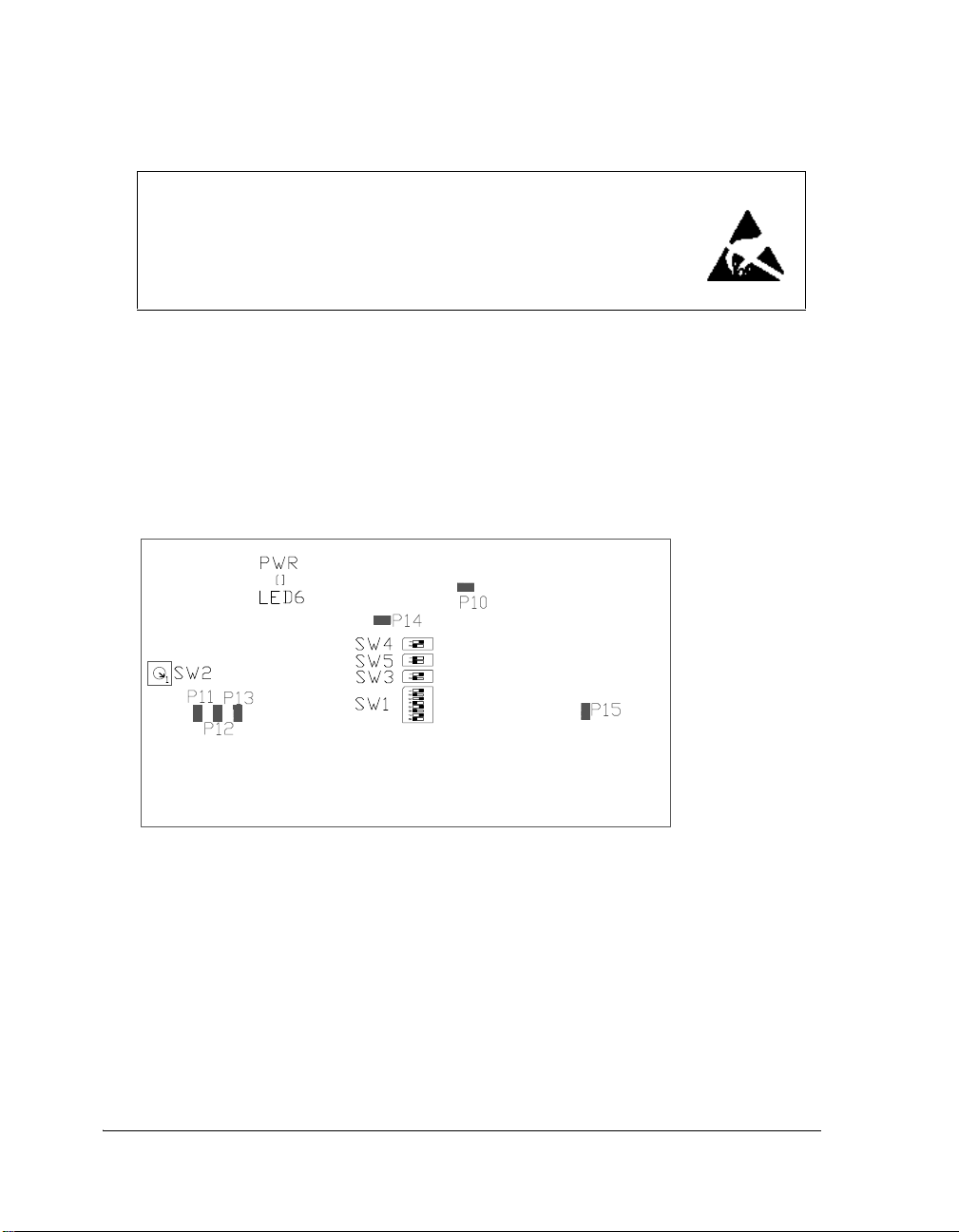
Figure 1-1 shows the default jumper and switch settings and LED used in
installation. There are four nylon standoffs in a bag included in the box.
They can be installed in the four corner mounting holes (
MH9) if desired. Place the nylon standoff in the hole and tighten a hex nut
MH1, MH7, MH8,
on each. Confirm that your board is in the default configuration before
using the board.
Figure 1-1. EZ-KIT Lite Hardware Setup
1-4 ADSP-BF609 EZ-KIT Lite Evaluation System Manual

Using ADSP-BF609 EZ-KIT Lite
Supported Operating Systems
CCES 1.0.0 is supported on the following operating systems:
•Windows® XP Professional SP3 (32-bit only)
• Windows Vista™ Business, Enterprise, or Ultimate SP2 (32-bit
only)
• Windows 7 Professional, Enterprise, or Ultimate (32- and 64-bit)
Windows Vista and Windows 7 users may experience User Access
Control (UAC) related errors if the software is installed into a protected location, such as Program Files or Program Files (x86).
We recommend installing the software in a non-UAC-protected
location.
System Requirements
Verify that your PC has these minimum requirements for the CCSE 1.0.0
installation:
• 2 GHz single-core processor
• 1 GB RAM
• 8 GB available disk space
• One open USB port
A faster disk drive decreases the build time, especially for a large
amount of source files.
ADSP-BF609 EZ-KIT Lite Evaluation System Manual 1-5

EZ-KIT Lite Installation
EZ-KIT Lite Installation
Follow these instructions to ensure correct operation of the product software and hardware.
Step 1: Attach the provided USB plugs (labeled Mini and Male) to the pro-
vided USB cable.
Step 2: Connect the EZ-KIT Lite board to a personal computer (PC) running CCES.
There are two connection options: using an Analog Devices emulator or
using the standalone debug agent.
Using an Emulator:
1. Plug one side of the assembled USB cable into the USB connector
of the emulator. Plug the other side into a USB port of the PC running CCES.
2. Attach the emulator to the header connector P1 (labeled JTAG) on
the EZ-KIT Lite board.
Using the Debug Agent:
1. Attach the standalone debug agent to connectors P1 and ZP1 of the
EZ-KIT Lite board.
2. Plug one side of the provided USB cable into the USB connector of
the debug agent ZP1 (labeled USB). Plug the other side of the cable
into a USB port of the PC running CCES.
1-6 ADSP-BF609 EZ-KIT Lite Evaluation System Manual

Using ADSP-BF609 EZ-KIT Lite
Step 3: Attach the provided cord and appropriate plug to the 5V power
adaptor.
1. Plug the jack-end of the assembled power adaptor into the power
connector
2. Plug the other side of the power adaptor into a power outlet. The
power LED (labeled LED6) lights green when power is applied to
the board.
3. Power the emulator. Plug the jack-end of the assembled power
adaptor into the emulator and plug the other side of the power
adaptor into a power outlet. The ENABLE/POWER indicator
lights green.
Step 4 (if connected through the debug agent): Verify that the yellow
USB monitor LED and the green power LED on the debug agent are both
on. This signifies that the board is communicating properly with the host
PC and ready to run CCES.
P18 (labeled 5V) on the EZ-KIT Lite board.
EZ-KIT Lite Session Startup
It is assumed that the CrossCore Embedded Studio software is installed
and running on your PC.
ADSP-BF609 EZ-KIT Lite Evaluation System Manual 1-7
Note: If you connect the board or emulator first (before installing
CCES) to the PC, the Windows driver wizard may not find the
board drivers.
1. Navigate to the CCES environment via the Start menu.
Note that CCES is not connected to the target board.

EZ-KIT Lite Session Startup
2. Use a debug configuration to connect to the EZ-KIT Lite board.
If a debug configuration exists already, select the appropriate
configuration and click Apply and Debug or Debug. Go to step 9.
To create a debug configuration:
• Click the down arrow next to the little bug icon, select
Debug Configurations, or
• Choose Run > Debug Configurations.
3. (To create a new debug configuration) Select CrossCore Embed-
ded Studio Application and click (New launch configuration).
The Select Processor page of the Session Wizard appears on the
screen.
4. Ensure Blackfin is selected in Processor family. In Processor type,
select ADSP-BF609. Click Next.
The Select Connection Type page of the Session Wizard appears
on the screen.
5. Select one of the following:
• For standalone debug agent connections, EZ-KIT Lite and
click Next.
• For emulator connections, Emulator and click Next.
The Select Platform page of the Session Wizard appears on the
screen.
1-8 ADSP-BF609 EZ-KIT Lite Evaluation System Manual

Using ADSP-BF609 EZ-KIT Lite
6. Do one of the following:
• For standalone debug agent connections, ensure that the
selected platform is ADSP-BF609 EZ-KIT Lite via Debug
Agent.
• For emulator connections, choose the type of emulator that
is connected to the board.
7. Click Finish to close the wizard.
The new debug configuration is created and added to the program(s) to load list.
8. In the Program(s) to load section, choose the program to load
when connecting to the board. If not loading any program upon
connection to the target, do not make any changes.
Note that while connected to the target, there is no way to choose a
program to download. To load a program once connected, terminate the session.
ADSP-BF609 EZ-KIT Lite Evaluation System Manual 1-9
To delete a configuration, go to the Debug Configurations dialog
box and select the configuration to delete. Click and choose Yes
when asked if you wish to delete the selected launch configuration.
Then Close the dialog box.
To disconnect from the target board, click the terminate button
(red box) or choose Run > Terminate.
To delete a session, choose Target > Session > Session List. Select
the session name from the list and click Delete. Click OK.

Evaluation License Restrictions
Evaluation License Restrictions
The ADSP-BF609 EZ-KIT Lite software is part of the EZ-Board BSP
(Board Support Package) for the Blackfin ADSP-BF60x family. The
EZ-KIT Lite is a licensed product that offers an unrestricted evaluation
license for 90 days after activation. Once the evaluation period ends, the
evaluation license becomes permanently disabled. If the evaluation license
is installed but not activated, it allows 10 days of unrestricted use and then
becomes disabled. The license can be re-enabled by activation.
An evaluation license can be upgraded to a full license. Licenses can be
purchased from:
• Analog Devices directly. Call (800) 262-5645 or 781-937-2384 or
go to:
http://www.analog.com/en/content/buy_online/fca.html.
• Analog Devices, Inc. local sales office or authorized distributor. To
locate one, go to:
http://www.analog.com/salesdir/continent.asp.
The EZ-KIT Lite hardware must be connected and powered up to
use CCES with a valid evaluation or full license.
Memory Map
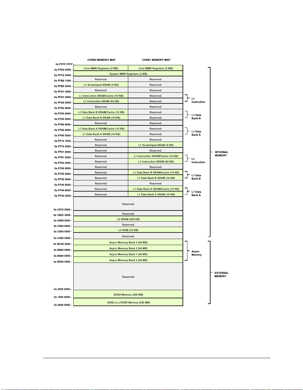
The ADSP-BF609 processor has a single unified 4G memory space for
instructions and data storage. See Figure 1-2. The processor’s memory
details can be found in the ADSP-BF60x Blackfin Processor Hardware
Reference.
1-10 ADSP-BF609 EZ-KIT Lite Evaluation System Manual
Using ADSP-BF609 EZ-KIT Lite
Figure 1-2. ADSP-BF609 Processor Memory Map
ADSP-BF609 EZ-KIT Lite Evaluation System Manual 1-11

DDR2 SDRAM
The board has a 16M x 16-bit burst flash memory connected to the processor’s Static Memory Controller (SMC). The processor also is connected
to a 32 Mb quad serial flash memory via the Serial Peripheral Interface
(SPI). Both flash memories can be used for non-volatile data storage and
processor boot.
DDR2 SDRAM
The ADSP-BF609 processor connects to a 128 MB Micron
MT47H64M16HR-3 chip through the Double Data Rate Synchronous
Dynamic Random-Access Memory (DDR2 SDRAM) controller. The
DDR2 memory controller on the processor and DDR2 memory chip are
powered by the on-board 1.8V regulator. Data is transferred between the
processor and DDR2 on both the rising and falling edges of the DDR2
clock. The DDR2 controller on the processor can operate at a maximum
clock frequency of 250 MHz.
With a CCES session running and connected to the EZ-KIT Lite via the
USB standalone debug agent, the DDR2 registers are configured automatically each time the processor is reset. The values are used whenever
DDR2 is accessed through the debugger (for example, when viewing
memory or loading a program).
To disable the automatic setting of the DDR2 registers, select Target
Options from the Session menu in CCES and uncheck Use XML reset
values.
An example program is included in the EZ-KIT Lite installation directory
to demonstrate how to setup and access the DDR2 interface. For more
information on how to initialize the registers after a reset, refer to the
hardware reference manual.
1-12 ADSP-BF609 EZ-KIT Lite Evaluation System Manual

Using ADSP-BF609 EZ-KIT Lite
SPI Interface
The ADSP-BF609 processor has two SPI interfaces, SPI0 and SPI1. SPI0 is
connected to a Winbond W25Q32BV 32 Mb serial flash memory with
dual and quad SPI support.
Quad mode is enabled by default. The processor flag signals, PD00 and
PD01 (SPI0 D2 and D3), can be disconnected by using SoftConfig. Refer to
“Software-Controlled Switches (SoftConfig)” on page 2-3 for more infor-
mation. By default, the SPI0 chip select 1 is connected to the memory
device. This can also be disconnected by using SoftConfig.
SMC Interface
The Static Memory Controller (SMC) interface of the ADSP-BF609
EZ-KIT Lite contains a 32 MB (16M x 16) Numonyx PC28F128P33B
parallel flash chip. Flash memory is connected to the 16-bit data bus and
address lines 1–23. Chip enable is decoded by using SMC0_AMS0.
The flash memory is bottom boot and provides One-Time-Programmable
(OTP) memory.
Flash memory is pre-loaded with boot code for the POST program. For
more information, refer to “Power-On-Self Test” on page 1-20.
Ethernet Interface
The ADSP-BF609 processor has two Reduced Media Independent Interfaces (RMIIs), one of which connects to an external Ethernet PHY device.
The EZ-KIT Lite provides a National DP83848C, Auto-MDIX, fully
compliant PHY with IEEE 802.2/802.2u standards. The PHY supports
10BASE-T and 100BASE-TX operations. The PHY and processor support
IEEE 1588 time stamping, available on the EZ-KIT Lite via a standard
ADSP-BF609 EZ-KIT Lite Evaluation System Manual 1-13

USB OTG HS Interface
RJ-45 connector. For more information, see “Ethernet Connector (J1)”
on page 2-27.
The MAC address is stored in parallel flash (U44) at address 0x0106
0000, and can be found on a sticker on the bottom side of the board.
Example programs are included in the EZ-KIT Lite installation directory
to demonstrate how to use the Ethernet interface.
If a program is written over this area of the flash, the MAC address
will be lost.
USB OTG HS Interface
The ADSP-BF609 processor has an integrated USB PHY, and the
EZ-KIT Lite provides a mini AB connector. A 48 MHz oscillator provides
the clocking for the high-speed USB 2.0 On-the-Go (OTG) interface.
The board allows 5V at 500 mA to a peripheral by enabling the FET
switch U50. The USB controller has native support for controlling the
FET through the USB_VBC signal.
A test point also is provided for the USB clock input of the processor. A
user can remove the series resistor and feed an external clock from a function generator.
Use the example programs in the EZ-KIT Lite installation directory to
learn about the processor’s device and host modes. For more information,
refer to the ADSP-BF60x Blackfin Processor Hardware Reference.
CAN Interface
The Controller Area Network (CAN) interface of the EZ-KIT Lite is connected to the NXP TJA1041 high-speed CAN transceiver. The transceiver
1-14 ADSP-BF609 EZ-KIT Lite Evaluation System Manual

Using ADSP-BF609 EZ-KIT Lite
is attached to the CAN0 port of the ADSP-BF609 processor via an RJ-11
connector. See “CAN Connector (J4)” on page 2-27.
The
PE02 programmable flag connects to the error and power on indica-
tion output of the CAN transceiver, CAN0. The transmit and receive pins
of the transceiver are connected to the dedicated CAN0 transmit and receive
pins of the processor.
To disconnect the CAN IC signals CAN0RX and CAN0_ERR, change the
appropriate settings via SoftConfig. See “Software-Controlled Switches
(SoftConfig)” on page 2-3.
Example programs are included in the EZ-KIT Lite installation directory
to demonstrate CAN circuit operation.
UART Interface
The ADSP-BF609 processor has two built-in universal asynchronous
transmitters (UARTs), with only UART0 connected to a UART line transmitter. UART0 has full RS-232 functionality via the Analog Devices
ADM3315 line driver and receiver (U39).
Pin PD07/UART0_TX/TM0_ACI3 of the processor is connected to the
ADM3315 device directly. Pin PD08/UART0_RX/TM0_ACI0 is connected as
well by the default setting of SoftConfig. (This can be changed by the
SoftConfig switch).
By default, UART0
RTS and CTS signals are not connected (but can be
through SoftConfig). The SoftConfig switches also allow the loopback of
CTS and RTS. UART CTS can be added as an input to the reset circuit
through SoftConfig. Pins 1, 4 and 6 of the UART connector (
J2) can be
enabled as an input to the on-board reset circuit through SoftConfig.
Refer to “Software-Controlled Switches (SoftConfig)” on page 2-3 for
more information.
ADSP-BF609 EZ-KIT Lite Evaluation System Manual 1-15

SD Interface
An example program demonstrating UART0 in POST is included in the
EZ-KIT Lite installation directory. Note that the loopback of
data is done through an external connector.
TX and RX
SD Interface
The ADSP-BF609 processor has a secure digital (SD) interface. The SD
interface consists of a clock pin, command pin, card detect pin, write protect pin, and an 8-bit data bus. SoftConfig controls the connection of
processor pins PG10 and PG13 to the card detect and write protect features
of the SD interface. Refer to “Software-Controlled Switches (SoftConfig)”
on page 2-3 and “SD Connector (J5)” on page 2-27for more details.
An example program is included in the EZ-KIT Lite installation directory
to demonstrate how to set up and access the SD interface.
Rotary Encoder Interface
The ADSP-BF609 processor has a built-in, up-down counter with support
for a rotary encoder. The three-wire rotary encoder interface connects to
the rotary switch (SW9). The rotary encoder can be turned clockwise for
the up function, counter clockwise for the down function, or can be
pushed towards the center of the board to clear the counter.
The rotary switch is a two-bit quadrature (gray code) counter with detent,
meaning that both the down signal (
gle when the count register increases on a rotation to the right. Upon
rotating to the left,
decreases.
If the processor pins are needed on the expansion interface III, disconnect
the rotary encoder switch via SoftConfig. See “Software-Controlled
Switches (SoftConfig)” on page 2-3 for details.
1-16 ADSP-BF609 EZ-KIT Lite Evaluation System Manual
CNT0_DG and CNT0_UD toggle, and the overall count
CNT0_DG) and up signal (CNT0_UD) tog-

Using ADSP-BF609 EZ-KIT Lite
An example program is included in the EZ-KIT Lite installation directory
to demonstrate how to set up and access the rotary encoder.
Temperature Sensor Interface
Two external pins (SYS_TDA and SYS_TDK) of the processor are connected
to an internal thermal diode. The EZ-KIT Lite uses ON Semiconductor
ADM1032 digital thermometer and under/over temperature alarm to
monitor the processor’s temperature as well as the thermal diodes inside
the ADM1032 device. The thermometer uses the I2C bus and flag pins of
the processor. The following software-controlled signals are used for temperature monitoring.
• TEMP_IRQ_EN (programmable flag pin PG9)
• TEMP_THERM_EN (programmable flag pin PB15)
The thermal limit flag is connected to an LED (LED5) for a visual alarm if
the temp exceeds the limit. The thermal limit flag and ADM1032 IRQ
connect to flag pins of the processor, but are nonessential for temperature
monitoring. Consequently, the software-controlled switches have these
signals disconnected from the ADSP-BF609 processor by default.
See “Thermal Limit LED (LED5)” on page 2-23 and “Software-Con-
trolled Switches (SoftConfig)” on page 2-3 for more information.
Example programs are included in the EZ-KIT Lite installation directory
to demonstrate temperature sensor operations.
Link Ports Interface
The ADSP-BF609 processor has four dedicated link ports. Each link port
has a clock pin, an acknowledgment pin, and eight data pins. The ports
can operate at up to 83 MHz and act as either a receiver or a transmitter.
ADSP-BF609 EZ-KIT Lite Evaluation System Manual 1-17

General-Purpose I/O (GPIO)
The ports are used to interface gluelessly to other ADSP-BF609 processors
which also have the link ports pins brought out.
The EZ-KIT Lite enables access to link ports 0 and 1 (referred to as
and LP1 in schematics) via connectors P8 and J3, respectively. Two
ADSP-BF609 EZ-KIT Lites can mate gluelessly via the link port connectors. The processors communicate via the link ports, all while performing
independent tasks on each of the EZ-KIT Lite. To loopback the link port
connectors on one EZ-KIT Lite or connect three or more EZ-KIT Lites,
obtain a standard, off the shelf connector from Samtec. For more information, see “Link Port /JTAG Connectors (J3 and P8)” on page 2-25.
By default, the EZ-KIT Lite boots from the parallel flash memory. Link
port 0 can be selected as the boot source by setting the boot mode select
switch (SW2) to position 6. See “Boot Mode Select Switch (SW2)” on
page 2-19.
General-Purpose I/O (GPIO)
Four LEDs are available via programmable pins PG14, PG15, PE14, and
PB11. The connections are on by default and can be shut off through
SoftConfig.
Two push buttons are available on programmable flags PB10 and PE01.
The push buttons are connected to the processor by default. Use SoftConfig to disconnect the push buttons. Refer to “Software-Controlled
Switches (SoftConfig)” on page 2-3 for more information.
LP0
JTAG Interface
The EZ-KIT Lite design enables a multi-processor JTAG session using
connectors
mode. In single-processor mode, create a CCES session based on a standalone debug agent or an external emulator. To use the EZ-KIT Lite in
1-18 ADSP-BF609 EZ-KIT Lite Evaluation System Manual
P8 and J3. By default, the board is set up in single-processor

Using ADSP-BF609 EZ-KIT Lite
multi-processor mode, install an external emulator. Only one external
emulator is required for the main EZ-KIT Lite; other EZ-KIT Lites in the
JTAG chain do not require an emulator. In this mode, create a CCES
platform based on the number of JTAG devices in the JTAG chain using
the CCES Target Configurator. Then create a session for the EZ-KIT Lite
based on the newly created platform.
For a dual ADSP-BF609 EZ-KIT Lite session, connect two EZ-KIT Lites
via connectors
J3 and P8. Flip one of the two EZ-KIT Lites by
180 degrees to allow the boards to mate. To switch between single- and
multi-processor modes, use DIP switches SW1 and SW3-5. The switch settings can be found in “JTAG Interface Switches (SW1, SW3–5)” on
page 2-18.
For three or more ADSP-BF609 EZ-KIT Lite sessions, connect each of
the boards with JTAG cables. The cables connect JTAG pins of each
board and put the EZ-KIT Lites in a JTAG serial chain. For three EZ-KIT
Lites, three JTAG cables are required. Similarly, for four EZ-KIT Lites,
four JTAG cables are required. Note that each respective EZ-KIT Lite
board also requires its own power supply.
The standalone debug agent can be replaced by an external emulator, such
as the Analog Devices high-performance USB-based emulator. Be careful
not to damage the connectors when removing the debug agent. The emulator is connected to P1 on the top side of the board. See “EZ-KIT Lite
Installation” on page 1-6 for more information.
Part numbers for Samtec standard, off the shelf link port cables can be
found in “Link Port /JTAG Connectors (J3 and P8)” on page 2-25.
For more information about emulators, contact Analog Devices or go to:
http://www.analog.com/en/processors-dsp/software-and-reference-designs/content/tools_product_overview/fca.html
.
ADSP-BF609 EZ-KIT Lite Evaluation System Manual 1-19

Power-On-Self Test
Power-On-Self Test
The Power-On-Self-Test Program (POST) tests all EZ-KIT Lite peripherals and validates functionality as well as connectivity to the processor.
Once assembled, each EZ-KIT Lite if fully tested for an extended period
of time with POST. All EZ-KIT Lite boards are shipped with POST preloaded into one of their on-board flash memories. The POST is executed
by resetting the board and pressing the proper push button(s). The POST
also can be used as a reference for a custom software design or hardware
troubleshooting. Note that the source code for the POST program is
included in the EZ-KIT Lite installation directory along with the
readme.txt file, which describes how the board is configured to run
POST.
Expansion Interface III
The Expansion Interface III (EI3) allows an Analog Devices
EZ-Extender® or a custom-design daughter board to be tested across various hardware platforms that have the same expansion interface.
The EI3 implemented on the ADSP-BF609 EZ-KIT Lite consists of five
connectors, P1A, P1B, P1C, P2A, and P3A. The connectors contain a majority of the processor's signals. For pinout information, go to “ADSP-BF609
EZ-KIT Lite Schematic” on page B-1. The mechanical dimensions of the
expansion connectors can be obtained by contacting “Technical or Cus-
tomer Support”.
For more information about daughter boards, visit the Analog Devices
Web site at:
http://www.analog.com/en/processors-dsp/Blackfin/processors/Blackfin_evaluation_kits/fca.html
Limits to current and interface speed must be taken into consideration
when using the EI3. Current for the EI3 can be sourced from the EZ-KIT
1-20 ADSP-BF609 EZ-KIT Lite Evaluation System Manual
.

Using ADSP-BF609 EZ-KIT Lite
Lite; therefore, the current should be limited to 200 mA for 5V and
300 mA for the 3.3V planes. If more current is required, then a separate
power connector and a regulator must be designed on the daughter card.
Additional circuitry can add extra loading to signals, decreasing their maximum effective speed.
Analog Devices does not support and is not responsible for the
effects of additional circuitry.
Power Architecture
The ADSP-BF609 EZ-KIT Lite has three primary voltage domains: 3.3V,
1.25V and 1.8V.
The Analog Devices ADP1864 controller provides 3.3V for the VDD_USB,
VDD_EXT, and the 3.3V power requirements of the board. The Analog
Devices ADP1715 regulator provides 1.8V for VDD_DMC. The processor’s
VDD_INT is regulated to 1.25V by the ADP2119 controller.
Power Measurements
Locations are provided for measuring the current draw from various power
planes. Precision 0.05 ohm shunt resistors are available on the
VDD_INT, VDD_DDR2, VDD_USB, 3.3V, and USB_VBUS voltage domains. For
current draw, the jumper is removed, voltage across the resistor can be
measured using an oscilloscope, and the value of the resistor can be measured using a precision multi-meter. Once voltage and resistance are
measured, the current can be calculated by dividing the voltage by the
resistance. For the highest accuracy, a differential probe should be used for
measuring the voltage across the resistor. For more information, refer to
“Power Jumpers” on page 2-21.
VDD_EXT,
ADSP-BF609 EZ-KIT Lite Evaluation System Manual 1-21

Example Programs
Example Programs
Example programs are provided with the ADSP-BF609 EZ-KIT Lite to
demonstrate various capabilities of the product. The programs are
installed with CCES and can be found in the CrossCore Embedded Studio directory. Refer to a readme file provided with each example for more
information.
Reference Design Information
A reference design info package is available for download on the Analog
Devices Web site. The package provides information on the design, layout, fabrication, and assembly of the EZ-KIT Lite.
The information can be found at:
http://www.analog.com/en/processors-dsp/blackfin/processors/board-design-database/resources/index.html.
1-22 ADSP-BF609 EZ-KIT Lite Evaluation System Manual

2 ADSP-BF609 EZ-KIT LITE
HARDWARE REFERENCE
This chapter describes the hardware design of the ADSP-BF609 EZ-KIT
Lite board.
The following topics are covered.
• “System Architecture” on page 2-2
Describes the board’s configuration and explains how the board
components interface with the processor.
• “Software-Controlled Switches (SoftConfig)” on page 2-3
Lists and describes the processor signals routed through the software-controlled switches.
• “Push Buttons and Switches” on page 2-17
Shows the locations and describes the push buttons and switches.
• “Power Jumpers” on page 2-21
Shows the locations and describes the configuration jumpers.
• “LEDs” on page 2-22
Shows the locations and describes the LEDs.
• “Connectors” on page 2-24
Shows the locations and provides part numbers for the on-board
connectors. In addition, the manufacturer and part number information is provided for the mating parts.
ADSP-BF609 EZ-KIT Lite Evaluation System Manual 2-1
System Architecture
ADSP-BF609
500 MHz
Dual Core
349-lead LFBGA
0.80mm 19x19mm pkg
JTAG
Port
25 MHz
Oscillator
Power
Regulation
SMC0
32 MB
Burst Flash
(16M x 16 )
CLK
JTAG
Conn
Quad SPI
Flash
32Mb
ADM3315
RS232
DB9
Conn
5V
PWR
IN
3.30V (Adjustable)
1.25V (Adjustable)
Expansion Interface III
PBs/LEDs
Ext
Clock
Test Point/
Crystal
128 MB
DDR2
(64M x 16)
DDR2
USB OTG
Circuitry
Ethernet
RMII
PHY
SD/MMC
Conn
Rotary
Encoder
Conn
ADM1032
Temp
Sensor
CAN
RJ11
Conn
TJA 1041
Transceiver
10/100
MAC
SPI
RJ45
CONN
USB
Mini
Conn
USB
2.0
(HS)
Temp
Sensor /
TWI
MMC
RSI
GP
COUNTER
GPIOs
CAN
2.0
UART
Link
Ports
1.80V (Adjustable)
Serial
Ports
EPPI
Ports
Link Port 0/
MPJTAG Out
Conn
DIP
SWTs
Link Port 1 /
MPJTAG In
Conn
EPPIs
UART
SPI
Power
ACM PWM
TWI
EBIU
Serial
Ports
GPIOs
USB
CLK
48 MHz
Oscillator
Ext
Clock
Test Point/
Crystal
System Architecture
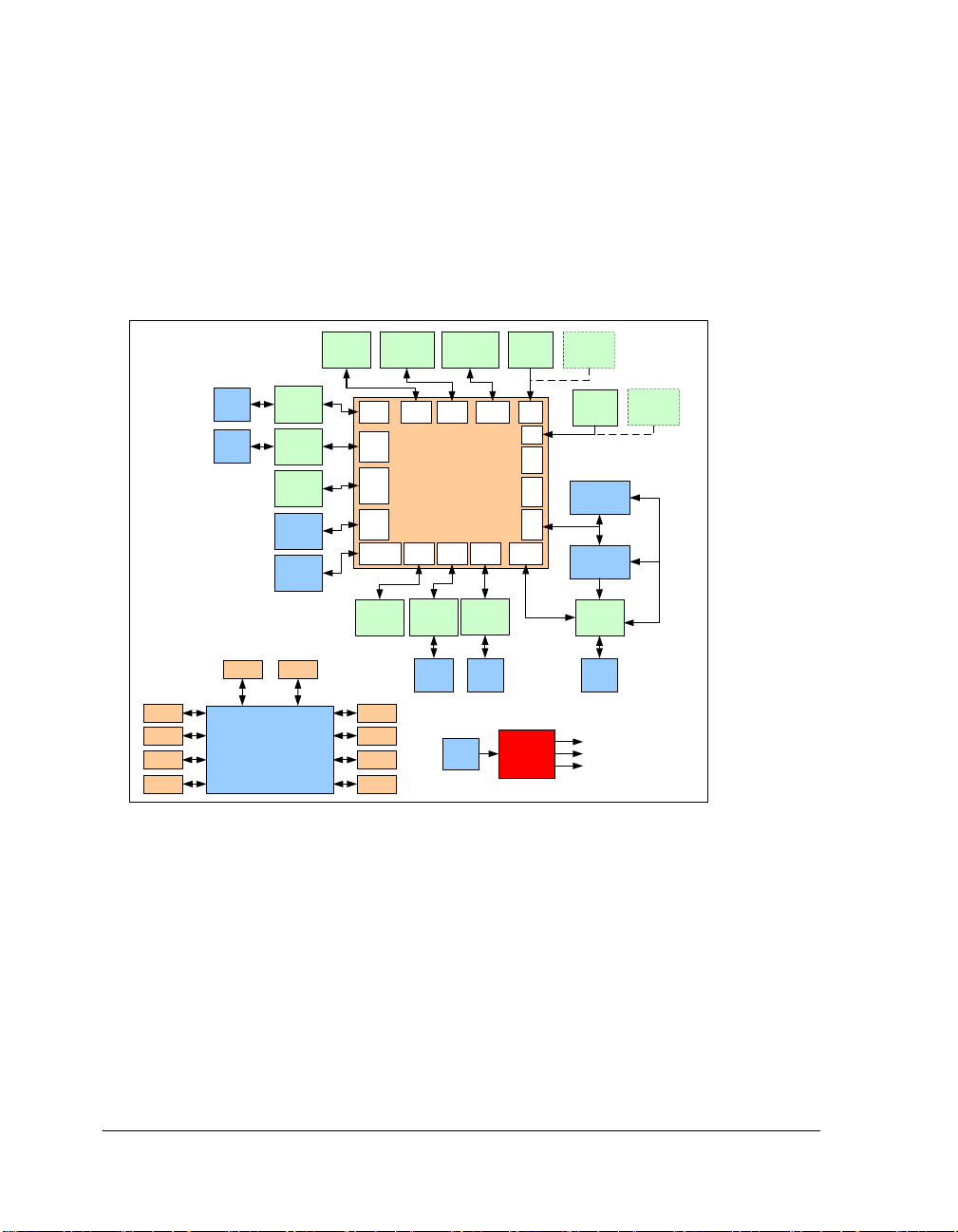
This section describes the processor’s configuration on the EZ-KIT Lite
board (Figure 2-1).
Figure 2-1. EZ-KIT Lite Block Diagram
The EZ-KIT Lite is designed to demonstrate the ADSP-BF609 Blackfin
processor’s capabilities.
The clock rate can be set up on the fly by the processor. The input clock is
25 MHz. The core clock runs at a maximum of 500 MHz. The default
boot mode for the processor is parallel flash boot. See “Boot Mode Select
Switch (SW2)” on page 2-19 for information on how to change the
default boot mode.
2-2 ADSP-BF609 EZ-KIT Lite Evaluation System Manual

ADSP-BF609 EZ-KIT Lite Hardware Reference
Software-Controlled Switches (SoftConfig)
On the ADSP-BF609 EZ-KIT Lite, most of the traditional mechanical
switches have been replaced by I2C software-controlled switches. The
remaining mechanical switches are provided for setting up a single- or
multiprocessor JTAG session, changing the boot mode, and push buttons.
Reference any SoftConfig*.c file found in the installation directory of
CCES for an example of how to set up the SoftConfig feature of the
ADSP-BF609 EZ-KIT Lite through software.
The SoftConfig section of this manual serves as a reference to any user
that intends to modify an existing software example. If software provided
from ADI is used there should be little need to reference this section.
Care should be taken when changing SoftConfig settings not to
create a conflict with interfaces. This is especially true when connecting extender cards. There is one possible conflict on the
EZ-KIT Lite when using SoftConfig—the wake push button must
be disconnected when using the SD card interface. The wake push
button is disabled by default, but if making changes, the signal
~WAKE_PUSHBUTTON_EN must be set to high if the SD card function is
desired.
Overview of SoftConfig
In order to further clarify the use of electronic single FET switches and
multi-channel bus switches, an example of each is illustrated and compared to a traditional mechanical switching solution. This is a generic
example that uses the same FET and bus switch components that are on
the EZ-KIT Lite. After this generic discussion there is a detailed explanation of the SoftConfig interface specific to the ADSP-BF609 EZ-KIT
Lite.
ADSP-BF609 EZ-KIT Lite Evaluation System Manual 2-3

Software-Controlled Switches (SoftConfig)
Figure 2-2 shows two individual FET switches (Pericom PI3A125CEX)
with reference designators UA and UB. Net names
B
control UA and UB. The default FET switch enable settings in this
ENABLE_A and ENABLE_
example are controlled by resistors RA and RB which pull the enable pin 1
of UA and UB to ground (low). In a real example, these enable signals are
controlled by the Microchip IO expander. The default pull-down resistors
connects the signals EXAMPLE_SIGNAL_A and EXAMPLE_SIGNAL_B and also
connects signals EXAMPLE_SIGNAL_C and EXAMPLE_SIGNAL_D. To disconnect
EXAMPLE_SIGNAL_A from EXAMPLE_SIGNAL_B, the Microchip IO expander is
used to change ENABLE_A to a logic 1 through software that interfaces with
the Microchip. The same procedure for ENABLE_B would disconnect
EXAMPLE_SIGNAL_C from EXAMPLE_SIGNAL_D.
Figure 2-2. Example of Individual FET Switches
Figure 2-3 shows the equivalent circuit to Figure 2-2 but utilizes mechan-
ical switches that are in the same package. Notice the default is shown by
black boxes located closer to the ON label of the switches. In order to disconnect these switches, physically move the switch to the
OFF position.
2-4 ADSP-BF609 EZ-KIT Lite Evaluation System Manual

ADSP-BF609 EZ-KIT Lite Hardware Reference
Figure 2-3. Example of Mechanical Switch Equivalent to Figure 2-2
Figure 2-4 shows a bus switch example, reference designator UC (Pericom
PI3LVD512ZHE), selecting between lettered functionality and numbered
functionality. The signals on the left side are multiplexed signals with
naming convention
letter_number. The right side of the circuit shows the
signals separated into letter and number, with the number on the lower
group (eg. 0B1) and the letter on the upper group (eg. 0B2). The default
setting is controlled by the signal CONTROL_LETTER_NUMBER which is pulled
low. This selects the number signals on the right to be connected to the
multiplexed signals on the left by default. In this example, the Microchip
IO expander is not shown but controls the signal CONTROL_LETTER_NUMBER
and allows the user to change the selection through software.
Figure 2-5 shows the equivalent circuit to Figure 2-4 but utilizes mechan-
ical switches. Notice the default for reference designators SWC and SWD is
illustrated by black boxes located closer to the ON label of the switches to
enable the number signals by default. Also notice the default setting for
reference designators
SWE and SWF is OFF. In order to connect the letters
instead of the numbers, the user physically changes all switches on SWC and
SWD to the OFF position and all switches on SWE and SEF to the ON position.
ADSP-BF609 EZ-KIT Lite Evaluation System Manual 2-5

Software-Controlled Switches (SoftConfig)
Figure 2-4. Example of Bus Switch
2-6 ADSP-BF609 EZ-KIT Lite Evaluation System Manual

ADSP-BF609 EZ-KIT Lite Hardware Reference
Figure 2-5. Example of Mechanical Switch Equivalent to Figure 2-4
SoftConfig on the ADSP-BF609 EZ-KIT LITE
The Microchip MCP23017 GPIO expander provides control for individual and 10-bit electronic switches. The TWI0 interface of the processor
communicates with the Microchip device. Two 10-bit switches, U40-41
are connected to the link port 1 and 0 interfaces, respectively. There are
an additional 27 individual switches with default settings that enable basic
board functionality.
Table 2-1 lists the ADSP-BF609 processor and EZ-KIT Lite interfaces
that are available by default. Note that only interfaces affected by software
switches are listed in Table 2-1.
ADSP-BF609 EZ-KIT Lite Evaluation System Manual 2-7
Software-Controlled Switches (SoftConfig)
Table 2-1. Default ADSP-BF609 Processor Interface Availability
Interface Availability by Default
EMAC0 Fully connected, need SoftConfig to enable RMII clock
Rotary encoder Enabled
Link port 0 Enabled with selection of the boot mode 6 setting, or by configuring
SoftConfig
CAN Enabled, the CAN0_ERR connection to the processor is disabled
UART
SMC (parallel flash) Enabled with selection of boot mode 1, can be changed with SoftConfig
SPI Flash Fully connected for quad mode by default
Temperature sensor Enabled, requires SoftConfig to connect interrupts
Push buttons Enabled (except for wake push button)
LEDs Enabled
TX, RX and RTS are enabled by default, use SoftConfig to enable other fea-
tures listed in the UART0 section and Table 2-5
Programming SoftConfig Switches
On the ADSP-BF609 EZ-KIT Lite, three Microchip MCP23017 devices
exist. Each of these devices have the following programming
characteristics:
• Each switch has two programmable GPIO registers.
GPIO Register Register Address
GPIOA 0x12
GPIOB 0x13
• Each GPIO register controls eight signals (software switches).
2-8 ADSP-BF609 EZ-KIT Lite Evaluation System Manual

ADSP-BF609 EZ-KIT Lite Hardware Reference
• By default, the Microchip MCP23017 GPIO signals function as
input signals.
The signals must be programmed as output signals to override their
default values. The following table shows the Microchip register
addresses and the values that must be written to them to program
the signals as output signals.
IODIR Register IODIR Register Address Value to be Written to Program Signals
as Outputs
IODIRA 0x00 0
IODIRB 0x01 0
Each of the examples in Cross Core Embedded Studio include source files
that program the soft switches, even if the default settings are being used.
The
README for each example identifies only the signals that are being
changed from their default values. The code that programs the soft
switches is located in the SoftConfig_BF609.c file in each example.
The following tables (Table 2-2, Table 2-3, and Table 2-4) outline the
default values for each of the three Microchip MCP23017 devices.
Table 2-2. I2C Hardware Address 0x21
GPIO MCP23017 Register Address Default Value
GPIOA 0x12 0x07
GPIOB 0x13 0xFC
Table 2-3. I2C Hardware Address 0x22
GPIO MCP23017 Register Address Default Value
GPIOA 0x12 0x0A
GPIOB 0x13 0x00
ADSP-BF609 EZ-KIT Lite Evaluation System Manual 2-9
Software-Controlled Switches (SoftConfig)
Table 2-4. I2C Hardware Address 0x23
GPIO MCP23017 Register Address Default Value
GPIOA 0x12 0x00
GPIOB 0x13 0x00
Page 12 of the “ADSP-BF609 EZ-KIT Lite Schematic” on page B-1
shows how the three Microchip GPIO expanders are connected to the
board’s ICs.
U41, a 10-bit bus switch, connects the link port 0 processor interface to J3
(link port connector) when the select input signal (pin 12) is high. By
default, the U41 select input is controlled by the boot mode switch (SW2).
When the boot mode switch is set to 1 (parallel flash boot), the select line
is high, enabling the system memory controller (SMC) signals, connected
through pins PA0-7 and PB0-1 of the processor. Setting the boot mode
switch to 6 (link port boot) drives the select line low and enables the link
port 0 connection to the J3 connector.
The U41 output selection, which is based on the boot mode selection, can
be overridden by the Microchip (U46) signal GPA0. This override is useful
in a case where the application needs to boot from parallel flash but then
use the link port 0 afterwards. After setting the signal high (to disable
U29), use GPA3 to control the output of U41.
The processor signals connected to
U41 can be disconnected from the link
port to support other features. The selection line must be low in order to
disconnect the signals from the link port connector
J3. This allows the
signals to connect to the on-board parallel flash memory and EI3 connectors. See “ADSP-BF609 EZ-KIT Lite Schematic” on page B-1 for details.
2-10 ADSP-BF609 EZ-KIT Lite Evaluation System Manual

ADSP-BF609 EZ-KIT Lite Hardware Reference
U40, a 10-bit bus switch, controls the link port 1 connection to P8 (link
port connector), EI3 (expansion interface), and SMC address signals. The
default setting is high, which connects the SMC address bus to the parallel
flash memory and connects the link port pins PA8-15 and PB2-3 to the
expansion interface. The link port 1 can be selected by setting U46 signal
GPA1 low.
Table 2-5 and Table 2-6 show the output signals of the Microchip GPIO
expander (U45), with a TWI address of 0100 001X, where X represents the
read or write bit. The signals that control an individual FET have an entry
under the FET column. The Component Connected column shows the
board IC that is connected if the FET is enabled. Note that some of the
Microchip (U45) output signals are connected directly to components on
the board. However, in most cases, the Microchip (U45) is controlling the
enable signal of a FET switch. Also note that if a particular functionality
of the processor signal is being used, it will be in bold font under the “Processor Signal” column.
Table 2-5. Output Signals of Microchip GPIO Expander
(U45 Port A)
Bit Signal Name Description FET Processor Signal
(if applicable)
0
CAN_EN Enable CAN IC, enabled by
default
1
~CAN_STB CAN standby control input U55 High
~CAN0_ERR_EN GPIO PE02 for CAN0 error U33 PE02/SPI1_
2
RDY/PPI0_
D22/SPT1_ACLK
~CAN0RX_EN CAN0RX connected to
3
CAN IC U55
~CNT0UD_EN Rotary counter 0 count up
4
connected to rotary connector
U34 PG04/SPT2_
ACLK/TM0_
TMR1/
CAN0_
/TM0_ACI2
RX
U30 PG11/SPT2_
BD1/TM0_
TMR6/CNT0_UD
Component
Connected
U55 High
U55 High
U55 Low
SW9 Low
Default
ADSP-BF609 EZ-KIT Lite Evaluation System Manual 2-11

Software-Controlled Switches (SoftConfig)
Table 2-5. Output Signals of Microchip GPIO Expander
(U45 Port A) (Cont’d)
Bit Signal Name Description FET Processor Signal
(if applicable)
5 ~CNT0DG_EN Rotary counter 0 count
down connected to rotary
connector
6
~CNT0ZM_EN Rotary counter 0 count zero
connected to rotary connector
7
RMII_CLK_EN RMII clock for EMAC0 dis-
U31 PG12/SPT2_
BD0/TM0_
TMR7/CNT0_DG
U32 PG07/SPT2_
BFS/TM0_
TMR5/CNT0_ZM
abled
Table 2-6. Output Signals of Microchip GPIO Expander
(U45 Port B)
Bit Signal Name Description FET Processor Signal
(if applicable)
0
~UART0RTS_EN UART0 RTS connected to
UART transceiver U39
1
~UART0RX_EN UART0 RX connected to
UART transceiver U39
2
~UART0CTS_EN UART0 CTS disconnected
from UART transceiver U39
by default
U21 PD09/~SPI0_
SEL5/UART0_
/SPI1_SEL4
RTS
U20 PD08/~UART0_
RX~/TM0_ACI0
U19 PD10/SPI0_
~UART0_
RDY/
CTS/SPI1_SEL3
Component
Default
Connected
SW9 Low
SW9 Low
U43 Low
Component
Default
Connected
U39 Low
U39 Low
U39
High
3
~UART0CTS_RTS_LPBK UART0 CTS and RTS not
U18 High
connected. Change to low
for looping back UART0
CTS and RTS signals
4
~UART0CTS_RST_EN UART0 CTS signal not con-
U17 High
nected to input of reset IC
(U48)
2-12 ADSP-BF609 EZ-KIT Lite Evaluation System Manual

ADSP-BF609 EZ-KIT Lite Hardware Reference
Table 2-6. Output Signals of Microchip GPIO Expander
(U45 Port B) (Cont’d)
Bit Signal Name Description FET Processor Signal
(if applicable)
5 ~UART0CTS_146_EN Allows pins 1, 4 and 6 of
UART connector (J2) to be
connected together and used
as input to reset IC (U48).
This is disabled by default.
6 ~TEMP_IRQ_EN PG09 can be used as TEMP
interrupt, disconnected by
default
7
~TEMP_THERM_EN PB15 can be used as TEMP
thermal limit, disconnected
by default
U16 High
U9 PG09/SPT2_
AD0/TM0_TMR4
U10 PB15/ETH0_
PTPPPS/PPI1_FS3
Component
Connected
U54 High
U54 High
Table 2-7 and Table 2-8 show the output signals of the Microchip GPIO
expander (
U46), with a TWI address of 0100 010X, where X represents the
read or write bit. The signals that control an individual FET have an entry
under the FET column. The Component Connected column shows the
board IC that is connected if the FET is enabled. Note that some of the
Microchip (U46) output signals are connected directly to components on
the board. However, in most cases, the Microchip (U46) is controlling the
enable signal of a FET switch. Also note that if a particular functionality
of the processor signal is being used, it will be in bold font under the “Processor Signal” column.
Default
Table 2-7. Output Signals of Microchip GPIO Expander
(U46 Port A)
Bit Signal Name Description FET Processor Signal
(if applicable)
0
OVERRIDE_SMC0_LP0_BOOT Overrides U41 select U29 Low
SMC0_EPPI2_LP1_SWITCH Controls U40 select line U28 High
1
Component
Connected
ADSP-BF609 EZ-KIT Lite Evaluation System Manual 2-13
Default

Software-Controlled Switches (SoftConfig)
Table 2-7. Output Signals of Microchip GPIO Expander
(U46 Port A) (Cont’d)
Bit Signal Name Description FET Processor Signal
(if applicable)
3 SMC0_LP0_EN Controls U41 select if
U28 High
Override High
4
~LED1_GPIO_EN PG14 is used as GPIO
output for LED1,
enabled by default
5
~LED2_GPIO_EN PG15 is used as GPIO
output for LED2,
enabled by default
6 ~LED3_GPIO_EN PE14 is used as GPIO
output for LED3,
enabled by default
7
~LED4_GPIO_EN PB11 is used as GPIO
output for LED4,
enabled by default
U27 PG14/~UART1_
RX~/~SYS_
IDLE1~/TM0_ACI1
U26 PG15/~UART1_
TX/SYS_
IDLE0~/SYS_
SLEEP/TM0_ACI4
U25 PE14/ETH1_
RXERR/SPT2_
ATDV/TM0_TMR0
U24 PB11/SMC0_
A25/SPT0_
BD0/TM0_ACLK3
Table 2-8. Output Signals of Microchip GPIO Expander
(U46 Port B)
Bit Signal Name Description FET Processor Signal
(if applicable)
~PUSHBUTTON1_EN PB10 is used as GPIO
0
input for push button 1,
enabled by default
1
~PUSHBUTTON2_EN PE01 is used as GPIO
input for push button 2,
enabled by default
2
~SD_CD_EN SD memory card detect
connected to GPIO
PG10, enabled by
default
U23 PB10/SMC0_
A24/SPT0_
BD1/TM0_ACLK0
U22 PE01/SPI1_
D2/PPI0_
D19/SPT1_BD0
U15 PG10/~UART1_
RTS~/SPT2_BCLK
Component
Default
Connected
LED1 Low
LED2 Low
LED3 Low
LED4 Low
Component
Default
Connected
SW6 Low
SW7 Low
J5 Low
2-14 ADSP-BF609 EZ-KIT Lite Evaluation System Manual

ADSP-BF609 EZ-KIT Lite Hardware Reference
Table 2-8. Output Signals of Microchip GPIO Expander
(U46 Port B) (Cont’d)
Bit Signal Name Description FET Processor Signal
(if applicable)
3 ~SD_WP_EN SD memory write pro-
tect connected to GPIO
PG10, enabled by
default
4
~SPIFLASH_CS_EN SPI flash chip select
SPI0SEL1 connection to
U38 SPI flash, connected
by default
5 ~SPI0D2_EN SPI flash data 2 connec-
tion to U38 SPI flash,
connected by default.
This is needed for quad
access mode.
6
~SPI0D3_EN SPI flash data 3 connec-
tion to U38 SPI flash,
connected by default.
This is needed for quad
access mode.
U14 PG13/~UART1_
CTS~/TM0_CLK
U13 PD11/~SPI0_
/SPI0_SS
SEL1
U12 PD00/SPI0_
D2/PPI1_
D16/~SPI0_SEL3
U16 PD01/SPI0_
/PPI1_
D3
D17/~SPI0_SEL2
Component
Connected
J5 Low
U38 Low
U38 Low
U38 Low
Table 2-9 and Table 2-10 show the output signals of the Microchip GPIO
expander (
U47), with a TWI address of 0100 011X, where X represents the
read or write bit. The signals that control an individual FET have an entry
under the FET column. The Component Connected column shows the
board IC that is connected if the FET is enabled.Note that some of the
Microchip (
U47) output signals are connected directly to components on
the board. However, in most cases, the Microchip (U47) is controlling the
enable signal of a FET switch. Also note that if a particular functionality
of the processor signal is being used, it will be in bold font under the “Processor Signal” column.
Default
ADSP-BF609 EZ-KIT Lite Evaluation System Manual 2-15

Software-Controlled Switches (SoftConfig)
Table 2-9. Output Signals of Microchip GPIO Expander (U47 Port A)
Bit Signal Name Description FET Processor Signal
(if applicable)
0
PHYINT_EN
1
Connects Ethernet 0
interrupt signal to
Ethernet PHY, con-
U35 PD06/~ETH0_
PHYINT~/PPI1_
FS2/TM0_ACI5
nected by default
1
PHY_PWR_DWN_INT
2
Controls power down
of the Ethernet PHY if
PHYINT_EN high
PHYAD0
3
Allows the PHY to be
2
placed in isolate mode
3
~ETHERNET_EN Disconnects EMAC0
signals from U49
~WAKE_PUSHBUTTON_EN Enables push button
4
input to processor
~PD0_SPI0D2_
5
EPPI1D16_SPI0SEL3_
EI3_EN
6
~PD1_SPI0D3_
EPPI1D17_SPI0SEL2_
EI3_EN
7
~PD2_SPI0MISO_EI3_
EN
Connects processor signal to EI3 connectors,
disabled by default
Connects processor signal to EI3 connectors,
disabled by default
Connects processor signal to EI3 connectors,
U7 PE12/~ETH1_
PHYINT~/PWM1_
CL/RSI0_D5
U36 PD00/SPI0_
D2/PPI1_
D16/~SPI0_SEL3
U51 PD01/SPI0_
D3/PPI1_
D17/~SPI0_SEL2
U57 PD02/SPI0_MISO EI3 High
disabled by default
Component
Default
Connected
U49 Low
U49 High-Z
U49 High-Z
U4/U5 Low
U1 High
EI3 High
EI3 High
1 This is an active low signal but the signal name does not show this.
2 This signal defaults to an input setting, putting the signal in High-Z. Must be used in concert with
PHYINT_EN. Set PHYINT_EN high first and then control PHY_PWR_DWN_INT.
3 This signal defaults to an input setting, putting the signal in High-Z. There is a 2.21k resistor pull-up,
which sets the PHY address appropriately. If isolate mode is desired, the signal needs to be set as an output and driven appropriately.
2-16 ADSP-BF609 EZ-KIT Lite Evaluation System Manual

ADSP-BF609 EZ-KIT Lite Hardware Reference
Table 2-10. Output Signals of Microchip GPIO Expander (U47 Port B)
Bit Signal Name Description FET Processor Signal
(if applicable)
0
~PD3_SPI0MOSI_EI3_EN Connects processor sig-
nal to EI3 connectors,
disabled by default
1
~PD4_SPI0CK_EI3_EN Connects processor sig-
nal to EI3 connectors,
disabled by default
U56 PD03/SPI0_MOSI EI3 High
U58 PD04/SPI0_CLK EI3 High
Component
Connected
Push Buttons and Switches
This section describes operation of the push buttons and switches. The
push button and switch locations are shown in Figure 2-6.
Default
Figure 2-6. Push Button and Switch Locations
ADSP-BF609 EZ-KIT Lite Evaluation System Manual 2-17

Push Buttons and Switches
JTAG Interface Switches (SW1, SW3–5)
The JTAG switches (SW1, SW3, SW4, and SW5) select between a single-processor (one board) and multi-processor (more than one board)
configurations. By default, the four DIP switches are set up for a single
EZ-KIT Lite configuration. See Table 2-11.
The default configuration applies to either a debug agent or an external
emulator, such as the Analog Devices high-performance USB-based emulator (HP-USB) or ICE-100B emulator.
To use an external emulator and multiple EZ-KIT Lites simultaneously in
one CrossCore Embedded Studio (CCES) multi-processor session, set up
the boards as shown in Table 2-12. Attach the boards to each other via
connectors J3 and P8. For two EZ-KIT Lites, no external cables are
required. For three or more EZ-KIT Lites, obtain Samtec JTAG cables
described in “Link Port /JTAG Connectors (J3 and P8)” on page 2-25.
Table 2-11. Single-Processor Configuration
Switch Position Single EZ-KIT Lite Use (Default)
SW1.1 ON
SW1.2 OFF
SW1.3 ON
SW1.4 OFF
SW1.5 ON
SW1.6 OFF
SW1.7 ON
SW1.8 OFF
SW3.1 ON
SW3.2 OFF
SW4.1 ON
SW4.2 OFF
2-18 ADSP-BF609 EZ-KIT Lite Evaluation System Manual

ADSP-BF609 EZ-KIT Lite Hardware Reference
Table 2-11. Single-Processor Configuration (Cont’d)
Switch Position Single EZ-KIT Lite Use (Default)
SW5.1 OFF
SW5.2 OFF
Table 2-12. Multiple-Processor Configuration
Switch Position Main EZ-KIT Lite
Attached to Emulator
SW1.1 ON OFF
SW1.2 ON ON
SW1.3 ON OFF
SW1.4 ON ON
SW1.5 ON OFF
SW1.6 ON ON
SW1.7 ON OFF
SW1.8 ON ON
SW3.1 ON OFF
SW3.2 OFF OFF
SW4.1 OFF OFF
SW4.2 ON ON
SW5.1 OFF ON
SW5.2 ON OFF
Boot Mode Select Switch (SW2)
EZ-KIT Lite
Not Attached to Emulator
The rotary boot mode select switch (SW2) determines the boot mode of the
processor. Table 2-13 shows the available boot mode settings. By default,
the ADSP-BF609 processor boots from 8-bit flash memory (parallel flash
boot).
ADSP-BF609 EZ-KIT Lite Evaluation System Manual 2-19

Push Buttons and Switches
Table 2-13. Boot Mode Select Switch (SW2)
SW2 Position Processor Boot Mode
0Idle—no boot
1 Parallel flash boot (default)
2RSI master boot
3 SPI0 master boot
4 SPI0 slave boot
5Reserved
6 Link port 0 slave boot
7 UART0 slave boot
IRQ/Flag Enable Switches (SW6–7)
The IRQ/flag enable switches (SW6–7) are push buttons which provide a
momentary low signal on processor signals PB10_A24_SP1D1 and PE1_
SPI1D2_EPPI0D19_SP3D0
switch.
when enabled through the software-controlled
Reset Switch (SW8)
The reset switch (SW8) is a push button which provides a reset pulse to the
ADSP-BF609 processor (U1), Ethernet PHY (U49), GPIO extenders
U45-47), and the expansion interface (EI3) connectors.
(
Rotary Encoder With Momentary Switch (SW9)
The rotary encoder (SW9) can be turned clockwise for an up count or
counter-clockwise for a down count. The encoder also features a momentary switch, activated by pushing the switch towards the center of the
board, that can be used to set the counter to zero. The rotary encoder is a
two-bit quadrature (Gray code) encoder.
2-20 ADSP-BF609 EZ-KIT Lite Evaluation System Manual

ADSP-BF609 EZ-KIT Lite Hardware Reference
The rotary encoder can be disconnected from the processor by setting
SoftConfig, see “Software-Controlled Switches (SoftConfig)” on page 2-3
for more information.
Wake Push Switch (SW10)
One of the wake input signals (PE12/~ETH1_PHYINT/PWM1_CL/RSI0_D5) is
connected to a push button switch (
default and can be enabled through SoftConfig. Refer to “Software-Con-
trolled Switches (SoftConfig)” on page 2-3 for more details.
SW10). This feature is disabled by
Power Jumpers
This section describes functionality of the power jumpers (P10-15).
Figure 2-7 shows the jumper locations.
Figure 2-7. Configuration Jumper Locations
ADSP-BF609 EZ-KIT Lite Evaluation System Manual 2-21

LEDs
Remove jumpers listed in Table 2-14 to measure the respective voltage
domain.
Table 2-14. Power Jumpers (P10-15)
Jumper Power Domain
P15 VDD_DMC
P14 VDD_INT
P13 3.3V
P12 VDD_EXT
P11 VDD_USB
P10 USB_VBUS
LEDs
This section describes the on-board LEDs. Figure 2-7 shows the LED
locations.
Figure 2-8. LED Locations
2-22 ADSP-BF609 EZ-KIT Lite Evaluation System Manual

ADSP-BF609 EZ-KIT Lite Hardware Reference
GPIO LEDs (LED1–4)
Four LEDs (LED1, LED2, LED3, and LED4) are connected to four general-purpose I/O pins of the processor (see Table 2-15). The LEDs are
active high and lit (amber) by writing a “1” to the corresponding programmable flag signal.
Table 2-15. GPIO LEDs
LED Reference Designator Processor Programmable Flag Pin
LED1 PG14
LED2 PG15
LED3 PE14
LED4 PB11
Thermal Limit LED (LED5)
The thermal limit LED (LED5) reports the status of the thermal sensor,
ADM1032 (U54). The thermal sensor monitors the processor’s temperature. When the high temperature limit set by the IC is violated, LED5 is
turned on (amber) as a visual indicator. The ADM1032 device has
built-in hysteresis, which causes the LED to de-activate only when the
temperature is significantly within the limit. For more information, see
“Temperature Sensor Interface” on page 1-17.
Power LED (LED6)
When LED6 is lit solid (green), it indicates that power is being supplied to
the board properly.
ADSP-BF609 EZ-KIT Lite Evaluation System Manual 2-23

Connectors
Components with a dotted outline are on the back side of the board
Reset LED (LED7)
When LED4 is lit (red), it indicates that the master reset of the processor is
active. The reset signal is controlled by the Analog Devices ADM13305
supervisory reset circuit.
SPD LED (LED6)
SPD LED indicates the speed of the Ethernet port. When LED6 is lit
(green), the speed is 100 Mb/s and when not lit, the speed is 10 Mb/s.
Connectors
This section describes connector functionality and provides information
about mating connectors. The connector locations are shown in
Figure 2-9.
Figure 2-9. Connector Locations
2-24 ADSP-BF609 EZ-KIT Lite Evaluation System Manual
ADSP-BF609 EZ-KIT Lite Hardware Reference
DCE UART Connector (J2)
The pinout of the J2 connector can be found in “ADSP-BF609 EZ-KIT
Lite Schematic” on page B-1.
Part Description Manufacturer Part Number
IDC header FCI 68737-410HLF
Mating Connector
IDC socket DIGI-KEY S4205-ND
Link Port /JTAG Connectors (J3 and P8)
The J3 and P8 connectors provide access to the Link Port and JTAG signals of the ADSP-BF609 processor. J3 supports link port 0 and the P8
connector is for link port 1.
Part Description Manufacturer Part Number
ERF8 10X2, RA female (J3) SAMTEC ERF8-010-01-S-D-RA-L
ERm8 10x2, RA male (P8) SAMTEC ERM8-010-01-S-D-RA-TR
Mating Cable
6" cable ERF8 to ERM8 10X2 SAMTEC ERCD-010-06.00-TBL-SBR-1
JTAG Connector (P1)
The JTAG interface of the ADSP-BF609 processor is connected to the
14-pin 0.1” header,
mating connector must have a plug. For more information, see “JTAG
Interface” on page 1-18.
Remove the standalone debug agent when an emulator is used with the
board. Follow the installation instructions provided in “EZ-KIT Lite
Installation” on page 1-6, using
ADSP-BF609 EZ-KIT Lite Evaluation System Manual 2-25
P1. Pin 3 is missing to provide keying. Pin 3 in the
P1 as the JTAG connection point.

Connectors
JTAG Connector (ZP1)
ZP1 is the connecting point for the SADA2 debug interface and is a 14-pin
0.1” header.
Expansion Interface III Connectors (P1A–C, P2A, P3A)
Five board-to-board connectors (P1A, P1B, P1C, P2A, and P3A) provide signals from the SPI, TWI, UART, SPORT, and GPIO interfaces of the
processor. The connectors are located on the bottom side of the board.
For more information, see “Expansion Interface III” on page 1-20.
Part Description Manufacturer Part Number
120-pin, 0.6 mm HIROSE FX8-120P-SV1(91)
Mating Connector
120-pin, 0.6 mm HIROSE FX8-120S-SV(21)
USB Connector (P7)
Part Description Manufacturer Part Number
USB mini-Ab MOLEX 56579-0576
Power Connector (P18)
Part Description Manufacturer Part Number
0.65 mm power jack CUI 045-0883R
Mating Connector
5.0VDC@3.6A power supply GLOBETEK GS-1750(R)
2-26 ADSP-BF609 EZ-KIT Lite Evaluation System Manual

ADSP-BF609 EZ-KIT Lite Hardware Reference
CAN Connector (J4)
Part Description Manufacturer Part Number
RJ-11 4-pin modular jack TYCO 5558872-1
Mating Cable
4-conductor modular jack cable L-COM TSP3044
SD Connector (J5)
Part Description Manufacturer Part Number
SD 8-bit, 2 GB SANDISK MHC-W21-601
Memory Card
2 GB SANDISK SDSDB-2048-A11
Ethernet Connector (J1)
Part Description Manufacturer Part Number
RJ-45 Ethernet jack Pulse Engineer PN J0011D21BNL
Mating Cable
Standard Ethernet cable
Ethernet Connectors (P16-17)
P16 and P17 allow connection to the Ethernet port IEEE 1588 signals.
They are 6-pin 0.1” headers. The pinout of the
can be found in “ADSP-BF609 EZ-KIT Lite Schematic” on page B-1.
ADSP-BF609 EZ-KIT Lite Evaluation System Manual 2-27
P16 and P17 connectors

Connectors
2-28 ADSP-BF609 EZ-KIT Lite Evaluation System Manual

A ADSP-BF609 EZ-KIT LITE BILL
OF MATERIALS
The bill of materials corresponds to “ADSP-BF609 EZ-KIT Lite Schematic”
on page B-1.
Ref. Qty. Description Reference
Designator
11 ADM708SARZ
SOIC8
2 1 ADM3315
TSSOP24
3 1 ADSP-BF609
BGA349C80P22X2
2_1900X1900
4 1 ADP1864AUJZ
SOT23-6
5 1 ADP1715 MSOP8 VR3 ADI ADP1715ARMZ-1.8-R7
6 1 74LVC14A SOIC14 U3 TI 74LVC14AD
7 1 IDT74FCT3244AP
Y SSOP20
8 2 SN74LVC1G08
SOT23-5
9 1 TJA1041 SOIC14 U55 NXP TJA1041T/VM,512
10 1 SN74LVC1G04
SOT23-5
U48 ADI ADM708SARZ
U39 ADI ADM3315EARUZ
U1 ADI ADSP-BF609-ENG
VR1 ADI ADP1864AUJZ-R7
U8 IDT IDT74FCT3244APYG
U52-U53 TI SN74LVC1G08DBVR
U59 TI SN74LVC1G04DBVT
Manufacturer Part Number
11 2 SN74CB3Q3245
TSSOP20
12 1 MIC2025-1 SOIC8 U50 DIGI-KEY 576-1057-ND
U4-U5 DIGI-KEY 296-19130-1-ND
ADSP-BF609 EZ-KIT Lite Evaluation System Manual A-1

Ref. Qty. Description Reference
Designator
Manufacturer Part Number
13 1 MT47H64M16
FBGA84
14 1 ADM1032
SOIC_N8
15 1 DP83848 LQFP48 U49 NATIONAL
16 1 50MHZ OSC012 U43 DIGI-KEY 300-8264-2-ND
17 33 PI3A125 SC70_5 U7,U9-U36,U51,
18 3 MCP23017
QFN65P600X600-2
9N
19 2 PI3LVD512
QFN50P350X900-4
3N
20 1 BF609
PC28F128P33B
U44
21 1 BF609 W25Q32
U38
22 1 SI7403BDN ICS010 U6 VISHAY SI7403BDN
U37 MICRON MT47H64M16HR-3 L
U54 ON SEMI ADM1032ARZ
DP83848CVV/NOPB
SEMI
PERICOM PI3A125CEX
U56-U58
U45-U47 DIGI-KEY MCP23017-E/ML-ND
U40-U41 PERICOM PI3LVD512ZHE
U44 MICRON PC28F128P33BF60D
U38 WINBOND W25Q32BVSSIG
23 1 25MHZ OSC003 U42 DIGI-KEY SG-8002CA-SCB-ND
24 1 48MHZ OSC003 U2 DIGI-KEY SG-8002CA-SCB-ND(48.00M)
25 1 ADP2119ACPZ-R7
DFN50P300X300-1
1N
26 1 DIP8 SWT016 SW1 C&K TDA08H0SB1
27 2 IDC 3X2
IDC3X2_SMT
28 1 DB9 9PIN CON038 J2 NORCOMP 191-009-213-L-571
VR2 ANA00 ADP2119ACPZ-R7
P16-P17 SAMTEC TSM-103-01-T-DV
A-2 ADSP-BF609 EZ-KIT Lite Evaluation System Manual

ADSP-BF609 EZ-KIT Lite Bill Of Materials
Ref. Qty. Description Reference
Designator
29 1 RJ11 4PIN
CON039
30 3 DIP2 SWT020 SW3-SW5 C&K CKN9064-ND
31 6 IDC 2X1 IDC2X1 P10-P15 FCI 90726-402HLF
32 1 3A RESETABLE
FUS004
33 6 IDC
2PIN_JUMPER_SH
ORT
34 1 PWR .65MM
CON045
35 1 USB_MINI-AB
5PIN CON052
36 4 MOMENTARY
SWT024
37 1 ROTARY_ENC_ED
GE SWT025
38 2 IDC 7x2
IDC7x2_SMTA
J4 TYCO 5558872-1
F1 TYCO SMD300F-2
SJ1-SJ6 DIGI-KEY S9001-ND
P18 DIG CP1-023-ND
P7 MOLEX 56579-0576
SW6-SW8,SW10 PANA-
SW9 PANA-
P1,ZP1 SAMTEC TSM-107-01-T-DV-A
Manufacturer Part Number
EVQ-Q2K03W
SONIC
EVQ-WKA001
SONIC
39 1 ROTARY SWT027 SW2 COPAL S-8110
40 1 ERM8 10X2
ERM8_10X2_SMT
41 1 ERF8 10X2
ERF8_10X2_SMT
42 1 RJ45 W/LEDS
CON065
43 1 SD_CONN 8-BIT
CON067
44 5 .6MM 120PIN
HIROSE_FX8-120P
-SV1(91)
P8 SAMTEC ERM8-010-01-S-D-RA-TR
J3 SAMTEC ERF8-010-01-S-D-RA-L-TR
J1 PULSE
ENG.
J5 MORETHA-
NALL
P1A,P1B,P1C,P2A,
P3A
HIROSE FX8-120P-SV1(91)
J0011D21BNL
MHC-W21-601-LF
ADSP-BF609 EZ-KIT Lite Evaluation System Manual A-3

Ref. Qty. Description Reference
Designator
Manufacturer Part Number
45 1 TEST LOOP
LOOP_2838
46 5 YELLOW LED001 LED1-LED5 DIGI-KEY P512TR-ND
47 3 600 100MHZ
500MA 1206
48 2 1UF 16V 10% 0805 C87-C88 DIGI-KEY 399-1284-2-ND
49 2 0 1/8W 5% 0805 R200,R211 VISHAY CRCW08050000Z0EA
50 1 190 100MHZ 5A
FER002
51 7 10UF 6.3V 10%
0805
52 1 4.7UF 6.3V 10%
0805
53 40 0.1UF 10V 10%
0402
GP1 KEYSTONE 5016
FER1-FER3 STEWARD HZ1206B601R-10
FER4 MURATA DLW5BSN191SQ2
C39,C117-C118,
C163-C164,
C177-C178
C90 AVX 08056D475KAT2A
C17-C18,
C41-C45,C84,
C95,C100,
C115-C116,
C135-C142,
C153-C162,
C173-C176,C186,
C188-C191,C200
AVX 08056D106KAT2A
AVX 0402ZD104KAT2A
54 124 0.01UF 16V 10%
0402
C1-C15,C19,
C22-C24,
C26-C38,C40,
C46-C61,
C64-C83,C94,
C96-C98,
C104-C107,
C111-C113,
C119-C134,
C143-C152,
C165-C172,
C179-C185,C192,
C198-C199
AVX 0402YC103KAT2A
A-4 ADSP-BF609 EZ-KIT Lite Evaluation System Manual

ADSP-BF609 EZ-KIT Lite Bill Of Materials
Ref. Qty. Description Reference
Designator
55 102 10K 1/16W 5%
0402
56 1 4.7K 1/16W 5%
0402
57 13 0 1/16W 5% 0402 R5-R6,R53,R120,
58 17 33 1/16W 5% 0402 R8,R13,R34,R37-
R9-R12,R17-R18,
R20-R33,R39-R48,
R50-R52,R56-R63,
R65-R67,R69-R72,
R80-R84,R89-R96,
R100-R101,R104R105,R107-R111,
R113,R118-R119,
R133-R135,R142,
R146,R148-R149,
R158-R160,R167,
R169-R170,R174,
R188,R205-R206,
R210,R218-R221,
R230-R235,R239
R64 VISHAY CRCW04024K70JNED
R136,R161-R162,
R165,R168,R228R229,R238,R240
R38,R54-R55,R85R86,R137-R138,
R140,R172-R173,
R227,R244-R245
Manufacturer Part Number
VISHAY CRCW040210K0FKED
PANASONIC
VISHAY CRCW040233R0JNEA
ERJ-2GE0R00X
59 1 1.5UH 20%
IND003
60 1 150UF 10V 10% D CT1 DIGI-KEY 478-3321-2-ND
61 2 2.2UF 10V 10%
0805
62 1 1A SK12
DO-214AA
63 2 107.0 1/10W 1%
0805
L2 COIL
CRAFT
C99,C101 AVX 0805ZD225KAT2A
D8 DIODES
INC
R190,R192 DIGI-KEY 311-107CRTR-ND
DO1608C-152MLC
B120B-13-F
ADSP-BF609 EZ-KIT Lite Evaluation System Manual A-5

Ref. Qty. Description Reference
Designator
Manufacturer Part Number
64 1 4.7UF 25V 20%
0805
65 1 68PF 50V 5% 0603 C91 AVX 06035A680JAT2A
66 1 470PF 50V 5% 0603 C92 AVX 06033A471JAT2A
67 1 220UF 6.3V 20%
D2E
68 1 1M 1/10W 5% 0603 R19 VISHAY CRCW06031M00FNEA
69 5 0.0 1/10W 1% 0603 R129,R214-R217 PHYCOMP 232270296001L
70 3 10 1/10W 5% 0603 R151-R152,R237 VISHAY CRCW060310R0JNEA
71 1 4700PF 16V 10%
0603
72 2 100PF 50V 5% 0603 C108-C109 AVX 06035A101JAT2A
73 10 2.21K 1/10W 1%
0603
74 2 62.0 1/10W 1%
0603
75 3 1UF 6.3V 20% 0402 C62-C63,C93 PANA-
C25 AVX 0805ZD475KAT2A
CT3 SANYO 10TPE220ML
C110 DIGI-KEY 311-1083-2-ND
R186-R187,R191,
R199,R201-R204,
R207-R208
R153-R154 DIGI-KEY 311-62.0HRTR-ND
DIGI-KEY 311-2.21KHRTR-ND
ECJ-0EB0J105M
SONIC
76 3 100 1/16W 5%
0402
77 1 24.9K 1/10W 1%
0603
78 3 10UF 10V 10%
0805
79 6 0.05 1/2W 1% 1206 R121,R124-R126,
80 2 10UF 16V 10%
1210
R87-R88,R141 DIGI-KEY 311-100JRTR-ND
R132 DIGI-KEY 311-24.9KHTR-ND
C16,C114,C187 PANA-
SONIC
SEI CSF 1/2 0.05 1%R
R144-R145
C86,C103 AVX 1210YD106KAT2A
ECJ-2FB1A106K
A-6 ADSP-BF609 EZ-KIT Lite Evaluation System Manual

ADSP-BF609 EZ-KIT Lite Bill Of Materials
Ref. Qty. Description Reference
Designator
81 2 GREEN LED001 LED6,LED8 PANA-
82 1 RED LED001 LED7 PANA-
83 2 1000PF 50V 5%
1206
84 1 255.0K 1/10W 1%
0603
85 1 80.6K 1/10W 1%
0603
86 3 5A MBRS540T3G
SMC
87 1 VARISTOR
V5.5MLA 30A 0603
88 1 THERM 0.5A 0.4
1206
89 1 2.5UH 30%
IND013
C85,C89 AVX 12065A102JAT2A
R130 VISHAY CRCW06032553FK
R131 VISHAY CRCW060380K6FKEA
D5-D7 ON SEMI MBRS540T3G
R1 LITTLE-
R209 LITTLE-
L1 COIL-
Manufacturer Part Number
SONIC
SONIC
FUSE
FUSE
CRAFT
LN1361CTR
LN1261CTR
V5.5MLA0603
1206L050-C
MSS1038-252NL_
90 7 330.0 1/16W 1%
0402
91 5 1.0K 1/16W 1%
0402
92 3 1.50K 1/16W 1%
0402
93 13 0 1/16W 5%
RNS005
94 3 22UF 16V 10%
1210
95 1 33 1/16W 5%
RNS003
R73-R79 DIGI-KEY 541-330LCT-ND
R2-R3,R155-R157 PANA-
SONIC
R15-R16,R175 PANA-
SONIC
RN1-RN13 PANA-
SONIC
C201-C203 YAIYO
YUDEN
RN14 PANA-
SONIC
ERJ-2RKF1001X
ERJ-2RKF1501X
EXB-28VR000X
EMK325BJ226KM-T
EXB-2HV330JV
ADSP-BF609 EZ-KIT Lite Evaluation System Manual A-7

Ref. Qty. Description Reference
Designator
Manufacturer Part Number
96 1 100.0 1/16W 1%
0402
97 2 0.036 1/2W 1%
1206
98 1 30A GSOT05
SOT23-3
99 2 30A GSOT03
SOT23-3
100 1 40A ESD5Z2.5T1
SOD-523
101 2 165.0 1/10W 1%
0603
102 1 220.0 1/10W 1%
0603
103 1 4.87K 1/10W 1%
0402
104 13 49.9 1/16W 1%
0402
105 1 15KV ESD7004
DFN50P250X100-1
0N
R4 DIGI-KEY 541-100LCT-ND
R127-R128 SUSUMU RL1632S-R036-F
D2 VISHAY GSOT05-GS08
D3-D4 VISHAY GSOT03-GS08
D1 ON SEMI ESD5Z2.5T1G
R197-R198 DIGI-KEY P165HTR-ND
R185 DIGI-KEY P220HTR-ND
R189 DIGI-KEY 541-4.87KHCT-ND
R176-R184,R193R196
D10 ON SEMI ESD7004MUTAG
STACKPOLE
RMCF0402FT49R9
106 1 15KV ESDA6V1SC
SOT95P280-6N
107 1 30K 1/10W 1%
0402
108 1 32.4K 1/10W 1%
0402
D9 DIGI-KEY 497-6637-1-ND
R242 PANA-
SONIC
R243 PANA-
SONIC
ERJ-2RKF3002X
ERJ-2RKF3242X
A-8 ADSP-BF609 EZ-KIT Lite Evaluation System Manual

IINDEX
A
ADSP-BF609 Blackfin processor, xii
ADSP-BF609 processor memory map, 1-11
architecture, of this EZ-KIT Lite, 2-2
B
bill of materials, A-1
board schematic (ADSP-BF609), B-1
boot
modes, 2-19
mode select switch (SW2), 2-19
bus switch, 2-5
example, 2-6
C
CAN connector (J4), 2-27
CAN interface, 1-14
configuration, of this EZ-KIT Lite, 1-3
connectors, 2-24
diagram of locations, 2-24
J1 (ethernet), 2-27
J2 (DCE UART), 2-25
J3 and P8 (Link Port / JTAG), 2-25
J4 (CAN), 2-27
J5 (SD), 2-27
P16-17 (ethernet), 2-27
P18 (power), 2-26
P1A-C (expansion), 2-26
P1 (JTAG), 2-25
P2A (expansion), 2-26
P3A (expansion), 2-26
P7 (USB), 2-26
ZP1 (JTAG), 2-26
contents, of this EZ-KIT Lite package, 1-2
customer support, xvii
D
DCE UART connector (J2), 2-25
DDR2 SDRAM controller, 1-12
default configuration, of this EZ-KIT Lite, 1-3
default jumper and switch settings, 1-4
default processor interface availability, 2-7
design reference info, 1-22
E
EngineerZone, xviii
ethernet
connector (J1), 2-27
connectors (P16-17), 2-27
ethernet interface, 1-13
example programs, 1-22
expansion interface, 1-20, 2-26
F
FET switches, 2-4
example, 2-4
ADSP-BF609 EZ-KIT Lite Evaluation System Manual I-1

Index
G
general-purpose I/O (GPIO), 1-18
general-purpose I/O pins (GPIO), 2-23
I
installation, of this EZ-KIT Lite, 1-4, 1-6
IRQ / Flag enable switches (SW6-7), 2-20
J
JTAG connector (P1), 2-25
JTAG connector (ZP1), 2-26
JTAG interface, 1-18
JTAG interface switches (SW1, SW3-5), 2-18
jumpers
diagram of locations, 2-21
L
LEDs, 2-22
diagram of locations, 2-22
LED1-4 (GPIO), 2-23
LED5 (thermal limit), 2-23
LED6 (power), 2-23
LED6 (SPD), 2-24
LED7 (reset), 2-24
license restrictions, xii, 1-10
Link Port / JTAG connectors (J3 and P8), 2-25
link ports interface, 1-17
M
mechanical switch, 2-5, 2-7
memory map, of this EZ-KIT Lite, 1-10
Micro Signal Architecture (MSA), xi
N
notation conventions, xx
O
operating systems, supported, 1-5
P
package contents, 1-2
power
architecture, 1-21
LED (LED6), 2-23
measurements, 1-21
power connector (P18), 2-26
power jumpers, 2-21
power-on-self test (POST), 1-20
product overview, xii
programming SoftConfig switches, 2-8
push buttons and switches, 2-17
R
Reduced Instruction Set Computing (RISC), xi
related documents, xix
reset
LEDs (LED7), 2-24
reset switch (SW8), 2-20
restriction, of the evaluation license, 1-10
rotary encoder interface, 1-16
rotary encoder switch (SW9), 2-20
S
schematic, of ADSP-BF609 EZ-KIT Lite, B-1
SD connector (J5), 2-27
SD interface, 1-16
SMC interface, 1-13
SoftConfig
on the EZ-KIT Lite, 2-7, 2-11
overview, 2-3
programming switches, 2-8
SPD
LEDs (LED6), 2-24
SPI interface, 1-13
I-2 ADSP-BF609 EZ-KIT Lite Evaluation System Manual

SRAM memory, 1-12
See also memory map
startup, of this EZ-KIT Lite, 1-7
supported operating systems, 1-5
SW1, SW3-5 (JTAG) interface switches, 2-18
SW10 (wake push) switch, 2-21
SW2 (boot mode select) switch, 2-19
SW6-7 (IRQ / Flag enable) switches, 2-20
SW8 (reset) switch, 2-20
SW9 (rotary encoder) switch, 2-20
switches
programming SoftConfig, 2-8
SW1, SW3-5 (JTAG interface), 2-18
SW10 (wake push), 2-21
SW2 (boot mode select), 2-19
SW6-7 (IRQ / Flag enable), 2-20
SW8 (reset), 2-20
SW (rotary encoder), 2-20
switches, diagram of locations, 2-17
system architecture, of this EZ-KIT Lite, 2-2
system requirements, 1-5
T
temperature sensor interface, 1-17
thermal limit
LED (LED5), 2-23
U
UART interface, 1-15
USB connector (P7), 2-26
USB OTG HS interface, 1-14
W
wake push switch (SW10), 2-21
ADSP-BF609 EZ-KIT Lite Evaluation System Manual I-3

Index
I-4 ADSP-BF609 EZ-KIT Lite Evaluation System Manual

A B C
D
1
1
2
2
ADSP-BF609 EZ-Board
SCHEMATIC
3
20 Cotton Road
3
ANALOG
Nashua, NH 03063
4
DEVICES
PH: 1-800-ANALOGD
4
Title
ADSP-BF609 EZ-Board
Title Block
Size Board No.
C
Date Sheet of
A B C D
1/5/12 16
A0269-2011
Rev
1.0
1
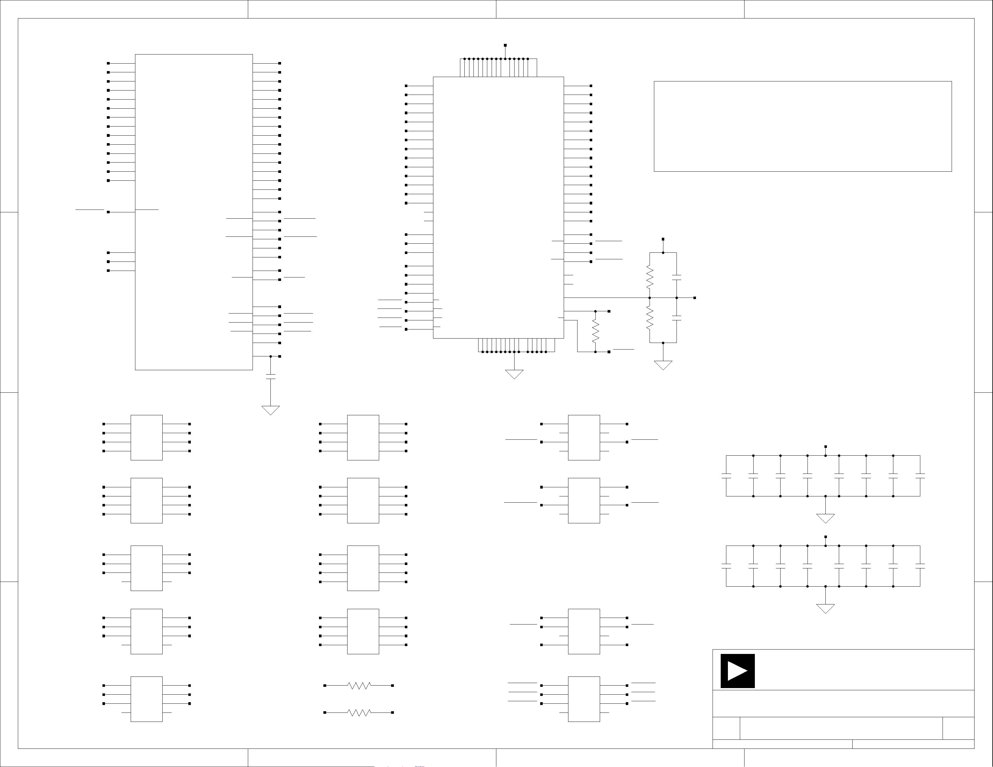
A B C
VDD_DMC
U1
Y21
DMC0_A00_Z
DMC0_A01_Z
DMC0_A02_Z
DMC0_A03_Z
DMC0_A04_Z
DMC0_A05_Z
1
DMC0_A06_Z
DMC0_A07_Z
DMC0_A08_Z
DMC0_A09_Z
DMC0_A10_Z
DMC0_A11_Z
DMC0_A12_Z
DMC0_A13_Z
DMC0_CS0_Z
DMC0_BA0_Z
DMC0_BA1_Z
DMC0_BA2_Z
DMC0_A00
U22
DMC0_A01
Y22
DMC0_A02
T20
DMC0_A03
W20
DMC0_A04
U21
DMC0_A05
W21
DMC0_A06
T21
DMC0_A07
W22
DMC0_A08
U20
DMC0_A09
R22
DMC0_A10
V22
DMC0_A11
T22
DMC0_A12
V21
DMC0_A13
F20
DMC0_CS0
R21
DMC0_BA0
V20
DMC0_BA1
R20
DMC0_BA2
2
DMC0_DQ00
DMC0_DQ01
DMC0_DQ02
DMC0_DQ03
DMC0_DQ04
DMC0_DQ05
DMC0_DQ06
DMC0_DQ07
DMC0_DQ08
DMC0_DQ09
DMC0_DQ10
DMC0_DQ11
DMC0_DQ12
DMC0_DQ13
DMC0_DQ14
DMC0_DQ15
DMC0_LDQS
DMC0_LDQS
DMC0_UDQS
DMC0_UDQS
DMC0_LDM
DMC0_UDM
DMC0_CK
DMC0_CK
DMC0_CKE
DMC0_CAS
DMC0_RAS
DMC0_WE
DMC0_ODT
VREF_DMC
M21
M22
P21
N22
N21
P22
L21
L22
F22
H21
E21
J22
J21
E22
H22
F21
K22
K21
G21
G22
K20
G20
M20
L20
P20
E20
H20
N20
J20
L19
DMC0_DQ00_Z
DMC0_DQ01_Z
DMC0_DQ02_Z
DMC0_DQ03_Z
DMC0_DQ04_Z
DMC0_DQ05_Z
DMC0_DQ06_Z
DMC0_DQ07_Z
DMC0_DQ08_Z
DMC0_DQ09_Z
DMC0_DQ10_Z
DMC0_DQ11_Z
DMC0_DQ12_Z
DMC0_DQ13_Z
DMC0_DQ14_Z
DMC0_DQ15_Z
DMC0_LDQS_Z
DMC0_LDQS_Z
DMC0_UDQS_Z
DMC0_UDQS_Z
DMC0_LDM_Z
DMC0_UDM_Z
DMC0_CK
DMC0_CK
DMC0_CKE_Z
DMC0_CAS_Z
DMC0_RAS_Z
DMC0_WE_Z
DMC0_ODT_Z
VREF_DMC
DMC0_A00
DMC0_A01
DMC0_A02
DMC0_A03
DMC0_A04
DMC0_A05
DMC0_A06
DMC0_A07
DMC0_A08
DMC0_A09
DMC0_A10
DMC0_A11
DMC0_A12
DMC0_A13
DMC0_BA0
DMC0_BA1
DMC0_BA2
DMC0_LDM
DMC0_UDM
DMC0_ODT
DMC0_CKE
DMC0_CS0
DMC0_RAS
DMC0_CAS
DMC0_WE
U37
M8
A0
M3
A1
M7
A2
N2
A3
N8
A4
N3
A5
N7
A6
P2
A7
P8
A8
P3
A9
M2
A10/AP
P7
A11
R2
A12
R8
RFU/A13
R3
RFU/A14
R7
RFU/A15
L2
BA0
L3
BA1
L1
BA2
F3
LDM
B3
UDM
K9 E2
K2
CKE
L8
CS
K7
RAS
CAS CK
K3
WE
MT47H64M16
FBGA84
C3
C1G9A9
VDDQ1
VDDQ2
VDDQ3
C7
VDDQ4
E9
C9
VDDQ5
VDDQ6
GNDQ1
GNDQ2
B2H8A7
G3
G1
VDDQ7
VDDQ8
GNDQ3
GNDQ4
B8
D2
G7
VDDQ9
VDDQ10
GNDQ5
GNDQ6
E7
D8
A1
VDD1
GNDQ7
GNDQ8
F8
F2
J9
E1
VDD2
VDD3
GNDQ10
GNDQ9
H2
M9
VDD4
R1
VDD5
GND1
A3
GND2
E3
J1
VDDL
GND3
J3
GND4
N1
GND5
P9
DQ0
DQ1
DQ2
DQ3
DQ4
DQ5
DQ6
DQ7
DQ8
DQ9
DQ10
DQ11
DQ12
DQ13
DQ14
DQ15
LDQS
LDQS
UDQS
UDQS
NC1
NC2ODT
VREF
CK
GNDL
J7
G8
G2
H7
H3
H1
H9
F1
F9
C8
C2
D7
D3
D1
D9
B1
B9
F7
E8
B7
A8
A2
J2
J8
K8L7
DMC0_DQ00
DMC0_DQ01
DMC0_DQ02
DMC0_DQ03
DMC0_DQ04
DMC0_DQ05
DMC0_DQ06
DMC0_DQ07
DMC0_DQ08
DMC0_DQ09
DMC0_DQ10
DMC0_DQ11
DMC0_DQ12
DMC0_DQ13
DMC0_DQ14
DMC0_DQ15
DMC0_LDQS
DMC0_LDQS
DMC0_UDQS
DMC0_UDQS
DMC0_CK
R4
100.0
0402
DMC0_CK
DDR2 end of line terminators and VTT tracking circuit have been
omitted since overall trace length is less than 2.5" for each net.
For a custom design, please adhere to any EE-note from ADI
and any recommendations by the memory manufacturer.
VDD_DMC
R2
1.0K
0402
R3
1.0K
0402
C17
0.1UF
0402
C18
0.1UF
0402
VREF_DMC
D
1
2
ADSP-BF609
BGA349C80P22X22_1900X1900
RN1
DMC0_A10_Z
DMC0_A12_Z
DMC0_A07_Z
DMC0_A01_Z
DMC0_A05_Z
3
DMC0_A11_Z
DMC0_A13_Z
DMC0_A08_Z
DMC0_A06_Z
DMC0_A02_Z
DMC0_A00_Z
1 8
2
R2A
3
R3A
4
R4A
0
RNS005
RN2
1 8
2
R2A
3
R3A
4
R4A
0
RNS005
RN3
1 8
2
R2A
3
R3A
4
R4A
R1BR1A
R2B
R3B
R4B
R1BR1A
R2B
R3B
R4B
R1BR1A
R2B
R3B
R4B
DMC0_A10
7
6
5
7
6
5
7
6
5
DMC0_A12
DMC0_A07
DMC0_A01
DMC0_A05
DMC0_A11
DMC0_A13
DMC0_A08
DMC0_A06
DMC0_A02
DMC0_A00
C84
0.1UF
0402
DMC0_DQ03_Z
DMC0_DQ04_Z
DMC0_DQ05_Z
DMC0_DQ02_Z
DMC0_DQ07_Z
DMC0_DQ06_Z
DMC0_DQ01_Z
DMC0_DQ00_Z
DMC0_DQ09_Z
DMC0_DQ14_Z
DMC0_DQ12_Z
DMC0_DQ11_Z
RN9
1 8
2
R2A
3
R3A
4
R4A
0
RNS005
RN8
1 8
2
R2A
3
R3A
4
R4A
0
RNS005
RN7
1 8
2
R2A
3
R3A
4
R4A
R1BR1A
R2B
R3B
R4B
R1BR1A
R2B
R3B
R4B
R1BR1A
R2B
R3B
R4B
CLK termination at the memory
RN10
DMC0_DQ03
7
6
5
7
6
5
7
6
5
DMC0_DQ04
DMC0_DQ05
DMC0_DQ02
DMC0_DQ07
DMC0_DQ06
DMC0_DQ01
DMC0_DQ00
DMC0_DQ09
DMC0_DQ14
DMC0_DQ12
DMC0_DQ11
DMC0_LDQS_Z
DMC0_LDQS_Z
DMC0_UDQS_Z
DMC0_UDQS_Z
1 8
2
R2A
3
R3A
4
R4A
0
RNS005
RN11
1 8
2
R2A
3
R3A
4
R4A
0
RNS005
R1BR1A
R2B
R3B
R4B
R1BR1A
R2B
R3B
R4B
DMC0_LDQS
7
6
5
7
6
5
DMC0_LDQS
DMC0_UDQS
DMC0_UDQS
C1
0.01UF
0402
C16
10UF
0805
C2
0.01UF
0402
C15
0.01UF
0402
C3
0.01UF
0402
C14
0.01UF
0402
VDD_DMC
C4
0.01UF
0402
VDD_DMC
C13
0.01UF
0402
C5
0.01UF
0402
C12
0.01UF
0402
C6
0.01UF
0402
C11
0.01UF
0402
C7
0.01UF
0402
C10
0.01UF
0402
C8
0.01UF
0402
C9
0.01UF
0402
3
0
RNS005
RN4
DMC0_A03
DMC0_A09
DMC0_A04
4
DMC0_BA1_Z
DMC0_BA0_Z
DMC0_BA2_Z
1 8
2
R2A
3
R3A
4
R4A
0
RNS005
RN5
1 8
2
R2A
3
R3A
4
R4A
0
RNS005
R1BR1A
R2B
R3B
R4B
R1BR1A
R2B
R3B
R4B
DMC0_A03_Z
7
6
5
7
6
5
DMC0_A09_Z
DMC0_A04_Z
DMC0_BA1
DMC0_BA0
DMC0_BA2
DMC0_DQ10_Z
DMC0_DQ13_Z
DMC0_DQ15_Z
DMC0_DQ08_Z
DMC0_LDM_Z
DMC0_UDM_Z
0
RNS005
RN6
1 8
2
R2A
3
R3A
4
R4A
0
RNS005
R6
0
0402
R5
0
0402
R1BR1A
R2B
R3B
R4B
7
6
5
DMC0_DQ10
DMC0_DQ13
DMC0_DQ15
DMC0_DQ08
DMC0_LDM
DMC0_UDM
DMC0_CKE_Z
DMC0_WE_Z
DMC0_ODT_Z
DMC0_RAS_Z
DMC0_CS0_Z
DMC0_CAS_Z
RN12
1 8
2
R2A
3
R3A
4
R4A
0
RNS005
RN13
1 8
2
R2A
3
R3A
4
R4A
0
RNS005
R1BR1A
R2B
R3B
R4B
R1BR1A
R2B
R3B
R4B
DMC0_CKE
7
6
5
DMC0_WE
DMC0_ODT
20 Cotton Road
ANALOG
Nashua, NH 03063
DMC0_RAS
7
6
5
DMC0_CS0
DMC0_CAS
Title
DEVICES
ADSP-BF609 EZ-Board
DSP DDR2 Interface
Size Board No.
C
Date Sheet of
1/5/12 16
PH: 1-800-ANALOGD
A0269-2011
Rev
1.0
2
4
A B C D
A B C
U1
A13
PA00/SMC0_A03/PPI2_D00/LP0_D0
PA01/SMC0_A04/PPI2_D01/LP0_D1
PA02/SMC0_A05/PPI2_D02/LP0_D2
PA03/SMC0_A06/PPI2_D03/LP0_D3
PA04/SMC0_A07/PPI2_D04/LP0_D4
PA05/SMC0_A08/PPI2_D05/LP0_D5
PA06/SMC0_A09/PPI2_D06/LP0_D6
1
PB00/SMC0_NORCLK/PPI2_CLK/LP0_CLK
PB03/SMC0_A16/PPI2_FS3/LP1_CLK
2
PB12/SMC0_BG/SPT0_BTDV/SPT0_AD1/TM0_ACLK1
PA07/SMC0_A10/PPI2_D07/LP0_D7
PA08/SMC0_A11/PPI2_D08/LP1_D0
PA09/SMC0_A12/PPI2_D09/LP1_D1
PA10/SMC0_A14/PPI2_D10/LP1_D2
PA11/SMC0_A15/PPI2_D11/LP1_D3
PA12/SMC0_A17/PPI2_D12/LP1_D4
PA13/SMC0_A18/PPI2_D13/LP1_D5
PA14/SMC0_A19/PPI2_D14/LP1_D6
PA15/SMC0_A20/PPI2_D15/LP1_D7
R228
0402
PB01/SMC0_AMS1/PPI2_FS1/LP0_ACK
PB02/SMC0_A13/PPI2_FS2/LP1_ACK
R229
0402
PB04/SMC0_AMS2/SMC0_ABE0/SPT0_AFS
PB05/SMC0_AMS3/SMC0_ABE1/SPT0_ACLK
PB06/SMC0_A21/SPT0_ATDV/TM0_ACLK4
PB07/SMC0_A22/PPI2_D16/SPT0_BFS
PB08/SMC0_A23/PPI2_D17/SPT0_BCLK
PB09/SMC0_BGH/SPT0_AD0/TM0_ACLK2
PB10/SMC0_A24/SPT0_BD1/TM0_ACLK0
PB11/SMC0_A25/SPT0_BD0/TM0_ACLK3
PB13/ETH0_TXEN/PPI1_FS1/TM0_ACI6
PB14/ETH0_REFCLK/PPI1_CLK
PB15/ETH0_PTPPPS/PPI1_FS3
PA00/SMC0_A03/PPI2_D00/LP0_D0
B13
PA01/SMC0_A04/PPI2_D01/LP0_D1
A12
PA02/SMC0_A05/PPI2_D02/LP0_D2
B12
PA03/SMC0_A06/PPI2_D03/LP0_D3
A11
PA04/SMC0_A07/PPI2_D04/LP0_D4
B11
PA05/SMC0_A08/PPI2_D05/LP0_D5
A10
PA06/SMC0_A09/PPI2_D06/LP0_D6
B10
PA07/SMC0_A10/PPI2_D07/LP0_D7
A9
PA08/SMC0_A11/PPI2_D08/LP1_D0
B9
PA09/SMC0_A12/PPI2_D09/LP1_D1
A8
PA10/SMC0_A14/PPI2_D10/LP1_D2
B8
PA11/SMC0_A15/PPI2_D11/LP1_D3
A7
PA12/SMC0_A17/PPI2_D12/LP1_D4
B7
PA13/SMC0_A18/PPI2_D13/LP1_D5
A6
PA14/SMC0_A19/PPI2_D14/LP1_D6
B6
PA15/SMC0_A20/PPI2_D15/LP1_D7
C12
0
PB00/SMC0_NORCLK/PPI2_CLK/LP0_CLK
C11
PB01/SMC0_AMS1/PPI2_FS1/LP0_ACK
C10
PB02/SMC0_A13/PPI2_FS2/LP1_ACK
C9
0
PB03/SMC0_A16/PPI2_FS3/LP1_CLK
C8
PB04/SMC0_AMS2/SMC0_ABE0/SPT0_AFS
C7
PB05/SMC0_AMS3/SMC0_ABE1/SPT0_ACLK
C6
PB06/SMC0_A21/SPT0_ATDV/TM0_ACLK4
A5
PB07/SMC0_A22/PPI2_D16/SPT0_BFS
B5
PB08/SMC0_A23/PPI2_D17/SPT0_BCLK
C5
PB09/SMC0_BGH/SPT0_AD0/TM0_ACLK2
A4
PB10/SMC0_A24/SPT0_BD1/TM0_ACLK0
B4
PB11/SMC0_A25/SPT0_BD0/TM0_ACLK3
C4
PB12/SMC0_BG/SPT0_BTDV/SPT0_AD1/TM0_ACLK1
K3
PB13/ETH0_TXEN/PPI1_FS1/TM0_ACI6
L3
PB14/ETH0_REFCLK/PPI1_CLK
M3
PB15/ETH0_PTPPPS/PPI1_FS3
PC13/SPI0_SEL6/PPI1_D13/ETH_PTPCLKIN
PD00/SPI0_D2/PPI1_D16/SPI0_SEL3
PD01/SPI0_D3/PPI1_D17/SPI0_SEL2
PD06/ETH0_PHYINT/PPI1_FS2/TM0_ACI5
PD09/SPI0_SEL5/UART0_RTS/SPI1_SEL4
PD10/SPI0_RDY/UART0_CTS/SPI1_SEL3
PD12/SPI1_SEL1/PPI0_D20/SPT1_AD1/SPI1_SS
PD15/SPI1_SEL2/PPI0_D21/SPT1_AD0
PC00/ETH0_RXD0/PPI1_D00
PC01/ETH0_RXD1/PPI1_D01
PC02/ETH0_TXD0/PPI1_D02
PC03/ETH0_TXD1/PPI1_D03
PC04/ETH0_RXERR/PPI1_D04
PC05/ETH0_CRS/PPI1_D05
PC06/ETH0_MDC/PPI1_D06
PC07/ETH0_MDIO/PPI1_D07
PC08/PPI1_D08
PC09/ETH1_PTPPPS/PPI1_D09
PC10/PPI1_D10
PC11/PPI1_D11/ETH_PTPAUXIN
PC12/SPI0_SEL7/PPI1_D12
PC14/SPI1_SEL7/PPI1_D14
PC15/SPI0_SEL4/PPI1_D15
PD02/SPI0_MISO
PD03/SPI0_MOSI
PD04/SPI0_CLK
PD05/SPI1_CLK/TM0_ACLK7
PD07/UART0_TX/TM0_ACI3
PD08/UART0_RX/TM0_ACI0
PD11/SPI0_SEL1/SPI0_SS
PD13/SPI1_MOSI/TM0_ACLK5
PD14/SPI1_MISO/TM0_ACLK6
K1
L2
L1
M2
M1
N2
N1
P2
P1
R2
R1
T2
T1
U2
U1
V2
V1
W2
Y2
Y1
W1
AB2
P3
R3
T3
U3
V3
AA1
W3
AA3
AB3
Y4
R227
0402
PC00/ETH0_RXD0/PPI1_D00
PC01/ETH0_RXD1/PPI1_D01
PC02/ETH0_TXD0/PPI1_D02
PC03/ETH0_TXD1/PPI1_D03
PC04/ETH0_RXERR/PPI1_D04
PC05/ETH0_CRS/PPI1_D05
PC06/ETH0_MDC/PPI1_D06
PC07/ETH0_MDIO/PPI1_D07
PC08/PPI1_D08
PC09/ETH1_PTPPPS/PPI1_D09
PC10/PPI1_D10
PC11/PPI1_D11/ETH_PTPAUXIN
PC12/SPI0_SEL7/PPI1_D12
PC13/SPI0_SEL6/PPI1_D13/ETH_PTPCLKIN
PC14/SPI1_SEL7/PPI1_D14
PC15/SPI0_SEL4/PPI1_D15
PD00/SPI0_D2/PPI1_D16/SPI0_SEL3
PD01/SPI0_D3/PPI1_D17/SPI0_SEL2
PD02/SPI0_MISO
PD03/SPI0_MOSI
33
PD05/SPI1_CLK/TM0_ACLK7
PD06/ETH0_PHYINT/PPI1_FS2/TM0_ACI5
PD07/UART0_TX/TM0_ACI3
PD08/UART0_RX/TM0_ACI0
PD09/SPI0_SEL5/UART0_RTS/SPI1_SEL4
PD10/SPI0_RDY/UART0_CTS/SPI1_SEL3
PD11/SPI0_SEL1/SPI0_SS
PD12/SPI1_SEL1/PPI0_D20/SPT1_AD1/SPI1_SS
PD13/SPI1_MOSI/TM0_ACLK5
PD14/SPI1_MISO/TM0_ACLK6
PD15/SPI1_SEL2/PPI0_D21/SPT1_AD0
PD04/SPI0_CLK
SYS_CLKOUT
SYS_MODE0
SYS_MODE1
SYS_MODE2
USB0_CLKIN
USB0_DP
USB0_DM
USB0_VBUS
USB0_ID
USB0_VBC
R161
0
0402
SYS_NMI/SYS_RESETOUT
SYS_CLKIN
SYS_XTAL
SYS_HWRST
SYS_PWRGD
SYS_EXTWAKE
U1
J3
SYS_BMODE0
H3
SYS_BMODE1
G3
SYS_BMODE2
C1
USB0_CLKIN
A3
USB0_DP
A2
USB0_DM
B1
USB0_VBUS
B3
USB0_ID
C2
USB0_VBC
H1
SYS_CLKIN
N3
SYS_CLKOUT
H2
SYS_XTAL
G2
SYS_HWRST
F3
SYS_NMI/SYS_RESETOUT
J2
SYS_PWRGD
K2
SYS_EXTWAKE
ADSP-BF609
BGA349C80P22X22_1900X1900
3.3V
TWI0_SCL
TWI0_SDA
TWI1_SCL
TWI1_SDA
SYS_TDA
SYS_TDK
JTG_EMU
JTG_TCK
JTG_TMS
JTG_TDI
JTG_TDO
JTG_TRST
SYS_FAULT
SYS_FAULT
C22
D22
C21
D21
Y12
Y11
E2
D3
E3
D1
D2
E1
F2
F1
D
TWI0_SCL
TWI0_SDA
TWI1_SCL
TWI1_SDA
SYS_TDA
SYS_TDK
0402
JTG_TCK
JTG_TMS
JTG_TDI
R244 33
0402
JTG_TRST
SYS_FAULT
SYS_FAULT
1
33R245
JTG_EMU
JTG_TDO
2
ADSP-BF609
BGA349C80P22X22_1900X1900
U1
AA4
PE00/SPI1_D3/PPI0_D18/SPT1_BD1
PE01/SPI1_D2/PPI0_D19/SPT1_BD0
PE02/SPI1_RDY/PPI0_D22/SPT1_ACLK
PE03/PPI0_D16/ACM0_FS/SPT1_BFS
PE04/PPI0_D17/ACM0_CLK/SPT1_BCLK
PE05/PPI0_D23/SPT1_AFS
PE06/SPT1_ATDV/PPI0_FS3/LP3_CLK
PE07/SPT1_BTDV/PPI0_FS2/LP3_ACK
PE08/PWM0_SYNC/PPI0_FS1/LP2_ACK/ACM0_T0
PE09/PPI0_CLK/LP2_CLK/PWM0_TRIP0
PE10/ETH1_MDC/PWM1_DL/RSI0_D6
PE11/ETH1_MDIO/PWM1_DH/RSI0_D7
3
PE12/ETH1_PHYINT/PWM1_CL/RSI0_D5
PE13/ETH1_CRS/PWM1_CH/RSI0_D4
PE14/ETH1_RXERR/SPT2_ATDV/TM0_TMR0
PE15/ETH1_RXD1/PWM1_BL/RSI0_D3
PF00/PWM0_AL/PPI0_D00/LP2_D0
PF01/PWM0_AH/PPI0_D01/LP2_D1
PF02/PWM0_BL/PPI0_D02/LP2_D2
PF03/PWM0_BH/PPI0_D03/LP2_D3
PF04/PWM0_CL/PPI0_D04/LP2_D4
PF05/PWM0_CH/PPI0_D05/LP2_D5
PF06/PWM0_DL/PPI0_D06/LP2_D6
PF07/PWM0_DH/PPI0_D07/LP2_D7
PF08/SPI1_SEL5/PPI0_D08/LP3_D0
PF09/SPI1_SEL6/PPI0_D09/LP3_D1
PF10/ACM0_A4/PPI0_D10/LP3_D2
PF11/PPI0_D11/LP3_D3/PWM0_TRIP1
PF12/ACM0_A2/PPI0_D12/LP3_D4
PF13/ACM0_A3/PPI0_D13/LP3_D5
PF14/ACM0_A0/PPI0_D14/LP3_D6
PF15/ACM0_A1/PPI0_D15/LP3_D7
4
SMC0_ARDY/SMC0_NORWT
SMC0_A1
SMC0_A2
SMC0_BR
PE00/SPI1_D3/PPI0_D18/SPT1_BD1
AB4
PE01/SPI1_D2/PPI0_D19/SPT1_BD0
Y5
PE02/SPI1_RDY/PPI0_D22/SPT1_ACLK
AA5
PE03/PPI0_D16/ACM0_FS/SPT1_BFS
AB5
PE04/PPI0_D17/ACM0_CLK/SPT1_BCLK
Y6
PE05/PPI0_D23/SPT1_AFS
Y7
PE06/SPT1_ATDV/PPI0_FS3/LP3_CLK
Y8
PE07/SPT1_BTDV/PPI0_FS2/LP3_ACK
Y9
PE08/PWM0_SYNC/PPI0_FS1/LP2_ACK/ACM0_T0
Y10
PE09/PPI0_CLK/LP2_CLK/PWM0_TRIP0
Y14
PE10/ETH1_MDC/PWM1_DL/RSI0_D6
Y15
PE11/ETH1_MDIO/PWM1_DH/RSI0_D7
Y13
PE12/ETH1_PHYINT/PWM1_CL/RSI0_D5
AB14
PE13/ETH1_CRS/PWM1_CH/RSI0_D4
AA16
PE14/ETH1_RXERR/SPT2_ATDV/TM0_TMR0
AA15
PE15/ETH1_RXD1/PWM1_BL/RSI0_D3
AA13
PF00/PWM0_AL/PPI0_D00/LP2_D0
AB13
PF01/PWM0_AH/PPI0_D01/LP2_D1
AA12
PF02/PWM0_BL/PPI0_D02/LP2_D2
AB12
PF03/PWM0_BH/PPI0_D03/LP2_D3
AA11
PF04/PWM0_CL/PPI0_D04/LP2_D4
AB11
PF05/PWM0_CH/PPI0_D05/LP2_D5
AA10
PF06/PWM0_DL/PPI0_D06/LP2_D6
AB10
PF07/PWM0_DH/PPI0_D07/LP2_D7
AA9
PF08/SPI1_SEL5/PPI0_D08/LP3_D0
AB9
PF09/SPI1_SEL6/PPI0_D09/LP3_D1
AA8
PF10/ACM0_A4/PPI0_D10/LP3_D2
AB8
PF11/PPI0_D11/LP3_D3/PWM0_TRIP1
AA7
PF12/ACM0_A2/PPI0_D12/LP3_D4
AB7
PF13/ACM0_A3/PPI0_D13/LP3_D5
AA6
PF14/ACM0_A0/PPI0_D14/LP3_D6
AB6
PF15/ACM0_A1/PPI0_D15/LP3_D7
D20
SMC0_ARDY/SMC0_NORWT
A14
SMC0_A1
B14
SMC0_A2
C13
SMC0_BR
ADSP-BF609
BGA349C80P22X22_1900X1900
PG04/SPT2_ACLK/TM0_TMR1/CAN0_RX/TM0_ACI2
PG05/ETH1_TXEN/RSI0_CMD/PWM1_SYNC/ACM0_T1
PG06/ETH1_REFCLK/RSI0_CLK/SPT2_BTDV/PWM1_TRIP0
PG15/UART1_TX/SYS_IDLE0/SYS_SLEEP/TM0_ACI4
PG00/ETH1_RXD0/PWM1_BH/RSI0_D2
PG01/SPT2_AFS/TM0_TMR2/CAN0_TX
PG02/ETH1_TXD1/PWM1_AL/RSI0_D1
PG03/ETH1_TXD0/PWM1_AH/RSI0_D0
PG07/SPT2_BFS/TM0_TMR5/CNT0_ZM
PG08/SPT2_AD1/TM0_TMR3/PWM1_TRIP1
PG09/SPT2_AD0/TM0_TMR4
PG10/UART1_RTS/SPT2_BCLK
PG11/SPT2_BD1/TM0_TMR6/CNT0_UD
PG12/SPT2_BD0/TM0_TMR7/CNT0_DG
PG13/UART1_CTS/TM0_CLK
PG14/UART1_RX/SYS_IDLE1/TM0_ACI1
SMC0_D0
SMC0_D1
SMC0_D2
SMC0_D3
SMC0_D4
SMC0_D5
SMC0_D6
SMC0_D7
SMC0_D8
SMC0_D9
SMC0_D10
SMC0_D11
SMC0_D12
SMC0_D13
SMC0_D14
SMC0_D15
SMC0_AMS0
SMC0_AOE/SMC0_NORDV
SMC0_AWE
SMC0_ARE
AA14
Y17
AB17
AB15
Y18
AA17
AB16
AA19
AA18
Y16
AB21
Y19
AB18
AA20
AB19
AB20
A15
B15
B18
A17
A18
B20
C14
A19
C17
B17
A20
C18
C15
B19
C19
B16
A16
B22
A21
C16
SMC0_D0
SMC0_D1
SMC0_D2
SMC0_D3
SMC0_D4
SMC0_D5
SMC0_D6
SMC0_D7
SMC0_D8
SMC0_D9
SMC0_D10
SMC0_D11
SMC0_D12
SMC0_D13
SMC0_D14
SMC0_D15
PG00/ETH1_RXD0/PWM1_BH/RSI0_D2
PG01/SPT2_AFS/TM0_TMR2/CAN0_TX
PG02/ETH1_TXD1/PWM1_AL/RSI0_D1
PG03/ETH1_TXD0/PWM1_AH/RSI0_D0
PG04/SPT2_ACLK/TM0_TMR1/CAN0_RX/TM0_ACI2
PG05/ETH1_TXEN/RSI0_CMD/PWM1_SYNC/ACM0_T1
PG06/ETH1_REFCLK/RSI0_CLK/SPT2_BTDV/PWM1_TRIP0
PG07/SPT2_BFS/TM0_TMR5/CNT0_ZM
PG08/SPT2_AD1/TM0_TMR3/PWM1_TRIP1
PG09/SPT2_AD0/TM0_TMR4
PG10/UART1_RTS/SPT2_BCLK
PG11/SPT2_BD1/TM0_TMR6/CNT0_UD
PG12/SPT2_BD0/TM0_TMR7/CNT0_DG
PG13/UART1_CTS/TM0_CLK
PG14/UART1_RX/SYS_IDLE1/TM0_ACI1
PG15/UART1_TX/SYS_IDLE0/SYS_SLEEP/TM0_ACI4
SMC0_D[0:15]
SMC0_AMS0
SMC0_AOE/SMC0_NORDV
SMC0_AWE
SMC0_ARE
SYS_NMI/SYS_RESETOUT
TWI1_SCL
TWI1_SDA
SMC0_BR
ANALOG
DEVICES
Title
Size Board No.
C
Date Sheet of
R27
10K
0402
R65
10K
0402
R66
10K
0402
R67
10K
0402
20 Cotton Road
Nashua, NH 03063
PH: 1-800-ANALOGD
ADSP-BF609 EZ-Board
DSP Signals
Rev
A0269-2011
1/5/12 16
3
1.0
3
4
A B C D

A B C
D
VDD_INT
F7D11
F8
F9
F10
F13
F14
F15
F16
G8
G9
G14
G15
T8
T9
T14
T15
U7
U8
U9
U10
U13
U14
U15
U16
F17
G16
G17
H16
H17
J17
K17
L17
M17
N17
P17
R16
R17
T16
T17
U17
VDD_INT
VDD_DMC
U1
A1
GND1
A22
GND2
B21
GND3
C20
GND4
D12
GND5
G1
GND6
J1
GND7
J9
GND8
J10
GND9
J11
GND10
J12
GND11
J13
GND12
J14
GND13
K8
GND14
K9
GND15
K10
GND16
K11
GND17
K12
GND18
K13
GND19
K14
GND20
K15
GND21
L8
GND22
L9
GND23
L10
GND24
L11
GND25
L12
GND26
L13
GND27
L14
GND28
L15
GND29
M8
GND30
M9
GND31
M10
GND32
ADSP-BF609
BGA349C80P22X22_1900X1900
GND33
GND34
GND35
GND36
GND37
GND38
GND39
GND40
GND41
GND42
GND43
GND44
GND45
GND46
GND47
GND48
GND49
GND50
GND51
GND52
GND53
GND54
GND55
GND56
GND57
GND58
GND59
GND60
GND61
GND62
GND63
M11
M12
M13
M14
M15
M19
N8
N9
N10
N11
N12
N13
N14
N15
P9
P10
P11
P12
P13
P14
W11
Y3
Y20
AA2
AA21
AA22
AB1
AB22
M4
B2
C3
R168
0
0402
C119
0.01UF
0402
C133
0.01UF
0402
C135
0.1UF
0402
3.3V
C120
0.01UF
0402
C134
0.01UF
0402
C136
0.1UF
0402
R166
10K
0402
DNP
TP3
C121
0.01UF
0402
C132
0.01UF
0402
C138
0.1UF
0402
VDD_INT
VDD_INT
C122
0.01UF
0402
C131
0.01UF
0402
C137
0.1UF
0402
C123
0.01UF
0402
C130
0.01UF
0402
C140
0.1UF
0402
C124
0.01UF
0402
C129
0.01UF
0402
C139
0.1UF
0402
C125
0.01UF
0402
C128
0.01UF
0402
C142
0.1UF
0402
C126
0.01UF
0402
C127
0.01UF
0402
C141
0.1UF
0402
VDD_EXT
U1
VDD_EXT1 VDD_INT1
F6
VDD_EXT2
F11
VDD_EXT3
F12
VDD_EXT4
G6
VDD_EXT5
W12
C116
0.1UF
0402
G7
VDD_EXT6
G10
VDD_EXT7
G11
VDD_EXT8
G12
VDD_EXT9
G13
VDD_EXT10
H6
VDD_EXT11
H7
VDD_EXT12
J6
VDD_EXT13
K6
VDD_EXT14
L4
VDD_EXT15
L6
VDD_EXT16
M6
VDD_EXT17
N6
VDD_EXT18
P6
VDD_EXT19
R6
VDD_EXT20
R7
VDD_EXT21
T6
VDD_EXT22
T7
VDD_EXT23
T10
VDD_EXT24
T11
VDD_EXT25
T12
VDD_EXT26
T13
VDD_EXT27
U6
VDD_EXT28
U11
VDD_EXT29
U12
VDD_EXT30
VDD_TD
E5
VDD_USB
1
2
VDD_USB
VDD_EXT
C114
10UF
0805
R165
0
0402
C115
0.1UF
0402
VDD_TD
VDD_INT2
VDD_INT3
VDD_INT4
VDD_INT5
VDD_INT6
VDD_INT7
VDD_INT8
VDD_INT9
VDD_INT10
VDD_INT11
VDD_INT12
VDD_INT13
VDD_INT14
VDD_INT15
VDD_INT16
VDD_INT17
VDD_INT18
VDD_INT19
VDD_INT20
VDD_INT21
VDD_INT22
VDD_INT23
VDD_INT24
VDD_DMC1
VDD_DMC2
VDD_DMC3
VDD_DMC4
VDD_DMC5
VDD_DMC6
VDD_DMC7
VDD_DMC8
VDD_DMC9
VDD_DMC10
VDD_DMC11
VDD_DMC12
VDD_DMC13
VDD_DMC14
VDD_DMC15
VDD_DMC16
VDD_INT
C117
10UF
0805
C118
10UF
0805
1
2
ADSP-BF609
BGA349C80P22X22_1900X1900
3
C144
0.01UF
0402
C143
0.01UF
0402
C145
0.01UF
0402
VDD_EXT
VDD_EXT
C146
0.01UF
0402
C147
0.01UF
0402
C148
0.01UF
0402
C149
0.01UF
0402
C150
0.01UF
0402
C152
0.01UF
0402
C151
0.01UF
0402
VDD_EXT
C163
10UF
0805
C164
10UF
0805
C171
0.01UF
0402
C172
0.01UF
0402
VDD_DMC VDD_DMC
C170
0.01UF
0402
C169
0.01UF
0402
C168
0.01UF
0402
C167
0.01UF
0402
C166
0.01UF
0402
R167
10K
0402
C165
0.01UF
0402
C176
0.1UF
0402
C175
0.1UF
0402
C173
0.1UF
0402
C174
0.1UF
0402
C177
10UF
0805
C178
10UF
0805
3
C160
0.1UF
0402
C159
0.1UF
0402
C157
0.1UF
0402
C158
0.1UF
0402
C155
0.1UF
0402
C156
0.1UF
0402
C153
0.1UF
0402
C154
0.1UF
0402
C162
0.1UF
0402
C161
0.1UF
0402
20 Cotton Road
ANALOG
Nashua, NH 03063
4
Title
DEVICES
ADSP-BF609 EZ-Board
PH: 1-800-ANALOGD
DSP Power and Ground
Size Board No.
C
Date Sheet of
1/5/12 16
A0269-2011
A B C D
4
Rev
1.0
4

A B C
D
3.3V
3.3V
SW1: Boot mode selection switch
SW2
2
1
0
7
6
SWT027
ROTARY
1
SYS_EXTWAKE
2
1C
3
2
4
4
5
R136
0
0402
R9
10K
0402
3.3V
R10
10K
0402
R12
10K
0402
R11
10K
0402
3.3V
U42
4
VDD
STANDBY OUT
GND
25MHZ
2
OSC003
SYS_MODE0
SYS_MODE1
SYS_MODE2
DSP OSC
31
3.3V
R13
33
0402
C22
0.01UF
0402
BMODE[2:0]
000
001
010
011
100
101
110
111
TP1
SYS_CLKIN
TP10
No-boot/Idle
Parrallel Flash boot
RSI master boot
SPI0 master boot
SPI0 slave boot
reserved
LP0 slave boot
UART0 slave boot
DEFAULT
SYS_NMI/SYS_RESETOUT
D9
1
IN0
IN1 GND0
4 5
6
IN3
ESDA6V1SC
SOT95P280-6N
GND1IN2
P17
IDC
1
3
3.3V
R15
1.50K
0402
R134
R135
10K
10K
0402
0402
P16
1
3
IDC
USB_VBUS
23
R209
THERM
1206
2
4
65
IDC3X2_SMT
C25
4.7UF
0805
R211
0
0805
R133
10K
0402
SYS_PWRGD
SYS_FAULT
SYS_FAULT
USB0_VBUS
PB15/ETH0_PTPPPS/PPI1_FS3
PC11/PPI1_D11/ETH_PTPAUXIN PC13/SPI0_SEL6/PPI1_D13/ETH_PTPCLKIN
TWI0_SCL
TWI0_SDA
SYS_TDA
SYS_TDK
2
4
65
IDC3X2_SMT
R16
1.50K
0402
U54
8
SCK
7
SI
2
D_PLUS
3
D_MINUS
ADM1032
ADM1032
SOIC_N8
3.3V
PC09/ETH1_PTPPPS/PPI1_D09
3.3V
3.3V
R18
1
VCC
GND
5
ALERT
THERM
10K
0402
6
4
3.3V
R17
10K
0402
C23
0.01UF
0402
1
TEMP_IRQ
TEMP_THERM
2
P7
"USB OTG"
USB_MINI-AB
OPTIONAL DSP CRYSTAL
3
SYS_XTAL
R14
0
0402
DNP
C21
18PF
0402
DNP
Y1
25MHz
OSC013
DNP
C20
18PF
0402
DNP
R212
0
0402
DNP
SYS_CLKIN
VBUS
D+
GND
SHELL
CON052
1
2
D-
3
4
ID
5
6
USB0_DM
USB0_DP
USB0_ID
R19
1M
0603
C24
0.01UF
0402
FER1
600
1206
Y2
24MHz
OSC013
DNP
R1
VARISTOR
0603
D10
1
IN0
IN1 GND0
4 8
5
IN3
6
NC0
7
NC1
ESD7004
DFN50P250X100-10N
R213
0
0402
DNP
32
GND1IN2
9
NC2
10
NC3
USB0_CLKIN
TEMP_IRQ_EN
PG09/SPT2_AD0/TM0_TMR4
TEMP_THERM_EN
PB15/ETH0_PTPPPS/PPI1_FS3
3.3V
R20
10K
0402
R21
10K
0402
U9
1
OE
2 4
PI3A125
SC70_5
U10
1
OE
2 4
PI3A125
SC70_5
BA
BA
TEMP_IRQ
TEMP_THERM
3
C193
18PF
0402
DNP
3.3V
3.3V
R7
10K
0402
R162
0
4
SYS_EXTWAKE
0402
DNP
U2
STANDBY OUT
48MHZ
OSC003
VDD
GND
4
2
USB OSC
31
R8
33
0402
TP2
USB0_CLKIN
TP11
3.3V
C19
0.01UF
0402
Title
C33
0.01UF
0402
ANALOG
DEVICES
C32
0.01UF
0402
C31
0.01UF
0402
ADSP-BF609 EZ-Board
C30
0.01UF
0402
20 Cotton Road
Nashua, NH 03063
PH: 1-800-ANALOGD
C29
0.01UF
0402
C28
0.01UF
0402
C26
0.01UF
0402
C27
0.01UF
0402
4
Temp. Sensor, Boot Switch, DSP Clock, USB Conn
USB OSC
Size Board No.
C
Date Sheet of
1/5/12 16
A0269-2011
A B C D
5
Rev
1.0

A B C
D
3.3V
3.3V
SD CARD
32 MB BURST FLASH
(16M x 16)
G4
D6
D5
H3
A6
U44
VCC1
A1
A2
A3
A4
A5
A6
A7
A8
A9
A10
A11
A12
A13
A14
A15
A16
A17
A18
A19
A20
A21
A22
A23
NC7
CE
OE
WE
RST
WP
ADV
VPEN
CLK
25
VCC2
GND1
B2
H4
VCCQ1
VCCQ2
VCCQ3
WAIT
NC1
NC2
NC3
NC4
NC5
NC6
GND2
GNDQ1
H2
R33
10K
0402
D0
D1
D2
D3
D4
D5
D6
D7
D8
D9
D10
D11
D12
D13
D14
D15
GNDQ2
H6
R34
33
0402
3.3V
F2
E2
G3
E4
E5
G5
G6
H7
E1
E3
F3
F4
F5
H5
G7
E7
F7
E8
B8
F1
G2
H1
B6
C34
0.01UF
0402
SMC0_D0
SMC0_D1
SMC0_D2
SMC0_D3
SMC0_D4
SMC0_D5
SMC0_D6
SMC0_D7
SMC0_D8
SMC0_D9
SMC0_D10
SMC0_D11
SMC0_D12
SMC0_D13
SMC0_D14
SMC0_D15
3.3V
R35
10K
0402
R138
DNP
33
0402
R36
10K
0402
DNP
3.3V
C35
0.01UF
0402
PD02/SPI0_MISOPD03/SPI0_MOSI
SMC0_A1
1
3.3V
R222
10K
0402
DNP
2
SMC0_AMS0
SYS_NMI/SYS_RESETOUT
PB00/SMC0_NORCLK/PPI2_CLK
R28
10K
0402
R29
10K
0402
PB06/SMC0_A21/SPT0_ATDV/TM0_ACLK4
PB08/SMC0_A23/PPI2_D17/SPT0_BCLK
PB10/SMC0_A24/SPT0_BD1/TM0_ACLK0
SMC0_AOE/SMC0_NORDV
3
R30
10K
0402
PD04/SPI0_CLK
SPIFLASH_CS
SPIFLASH_SPI0D2
SPIFLASH_SPI0D3
R42
10K
0402
PA00/SMC0_A03/PPI2_D00
PA01/SMC0_A04/PPI2_D01
PA02/SMC0_A05/PPI2_D02
PA03/SMC0_A06/PPI2_D03
PA04/SMC0_A07/PPI2_D04
PA05/SMC0_A08/PPI2_D05
PA06/SMC0_A09/PPI2_D06
PA07/SMC0_A10/PPI2_D07
PA08/SMC0_A11/PPI2_D08
PA09/SMC0_A12/PPI2_D09
PB02/SMC0_A13/PPI2_FS2
PA10/SMC0_A14/PPI2_D10
PA11/SMC0_A15/PPI2_D11
PB03/SMC0_A16/PPI2_FS3
PA12/SMC0_A17/PPI2_D12
PA13/SMC0_A18/PPI2_D13
PA14/SMC0_A19/PPI2_D14
PA15/SMC0_A20/PPI2_D15
PB07/SMC0_A22/PPI2_D16/SPT0_BFS
3.3V
R31
10K
0402
SMC0_A2
SMC0_ARE
SMC0_AWE
R223
10K
0402
DNP
R32
10K
0402
U38
SI SO
6
SCK
1
CS
3
WP
7
HOLD
W25Q32
SO8W
32Mb QUAD SPI FLASH
A1
B1
C1
D1
D2
A2
C2
A3
B3
C3
D3
C4
A5
B5
C5
D7
D8
A7
B7
C7
C8
A8
G1
H8
B4
F8
G8
D4
C6
F6
A4
E6
PC28F128P33B
EBGA64
8
VCC
GND
4
PG02/ETH1_TXD1/PWM1_AL/RSI0_D1
PE15/ETH1_RXD1/PWM1_BL/RSI0_D3SMC0_D[0:15]
PG03/ETH1_TXD0/PWM1_AH/RSI0_D0
PG00/ETH1_RXD0/PWM1_BH/RSI0_D2
PE13/ETH1_CRS/PWM1_CH/RSI0_D4
PE12/ETH1_PHYINT/PWM1_CL/RSI0_D5
PE10/ETH1_MDC/PWM1_DL/RSI0_D6
PE11/ETH1_MDIO/PWM1_DH/RSI0_D7
PG06/ETH1_REFCLK/RSI0_CLK/SPT2_BTDV/PWM1_TRIP0
PG05/ETH1_TXEN/RSI0_CMD/PWM1_SYNC/ACM0_T1
R139
0
0402
DNP
R137
33
U59
SN74LVC1G04
SOT23-5
C36
0.01UF
0402
C37
0.01UF
0402
0402
C38
0.01UF
0402
4
RN14
R1A R1B
R2A R2B
R3A R3B
R4A R4B
R5A R5B
R6A R6B
R7A R7B
R8A R8B
33
RNS003
SMC0_ARDY/SMC0_NORWT
161
152
143
134
125
116
107
98
MMC_D1
MMC_D3
MMC_D0
MMC_D2
MMC_D4
MMC_D5
MMC_D6
MMC_D7
PG10/UART1_RTS/SPT2_BCLK
PG13/UART1_CTS/TM0_CLK
PD11/SPI0_SEL1/SPI0_SS
PD00/SPI0_D2/PPI1_D16/SPI0_SEL3
PD01/SPI0_D3/PPI1_D17/SPI0_SEL2
MMC_D0
MMC_D1
MMC_D2
MMC_D3
MMC_D4
MMC_D5
MMC_D6
MMC_D7
R38 33
0402
R37 33
0402
SD_CD
SD_WP
SD_CD_EN
SD_WP_EN
SPIFLASH_CS_EN
SPI0D2_EN
SPI0D3_EN
R39
10K
0402
R22
10K
0402
R40
10K
0402
R23
10K
0402
R41
10K
0402
R24
10K
0402
R25
10K
0402
ANALOG
DEVICES
J5
7
DAT0
8
DAT1
9
DAT2
1
DAT3
10
DAT4
11
DAT5
12
DAT6
13
DAT7
5
CLK
2
CMD
22
MINI_SD_DAT0
23
MINI_SD_DAT1
24
MINI_SD_DAT2
16
MINI_SD_DAT3
20
MINI_SD_CLK
17
MINI_SD_CMD
15
CD
14
WP
CON067
SD_CONN
"SD CARD"
U15
1
OE
2 4
PI3A125
SC70_5
U14
1
OE
2 4
PI3A125
SC70_5
U13
1
OE
2 4
PI3A125
SC70_5
U12
1
OE
2 4
PI3A125
SC70_5
U11
1
OE
2 4
PI3A125
SC70_5
R26
10K
0402
20 Cotton Road
Nashua, NH 03063
PH: 1-800-ANALOGD
3.3V
4
3
BA
BA
BA
BA
BA
19
VDD1
VDD2
GND1
GND2
6
18
GND3
GND4
GND5
GND6
28
27
21
SD_CD
SD_WP
SPIFLASH_CS
SPIFLASH_SPI0D2
SPIFLASH_SPI0D3
C40
0.01UF
0402
C39
10UF
0805
1
2
3
4
Title
ADSP-BF609 EZ-Board
Memory
Size Board No.
C
Date Sheet of
A B C D
1/5/12 16
A0269-2011
Rev
1.0
6

A B C
3.3V
D
UART 0
3.3V
3.3V
R52
10K
0402
1
UART0RTS_EN
PD09/SPI0_SEL5/UART0_RTS/SPI1_SEL4
UART0RX_EN
PD08/UART0_RX/TM0_ACI0
R47
10K
0402
R49
10K
0402
DNP
U21
1
OE
2 4
PI3A125
SC70_5
U20
1
OE
2 4
PI3A125
SC70_5
R48
10K
0402
BA
BA
R50
10K
0402
R51
10K
0402
PD07/UART0_TX/TM0_ACI3
R53 0
0402
R54 33
0402
R55 33
0402
C41
0.1UF
0402
C42
0.1UF
0402
R56
10K
0402
R57
10K
0402
U39
6
C1+
20
C1-
2
C2+
4
C2-
5
EN
19
SD
7
T1IN
8
T2IN
9
T3IN
10
R1OUT
11
R2OUT
12
R3OUT
ADM3315
TSSOP24
V+
C3+
C3-
T1OUT
T2OUT
T3OUT
R1IN
R2IN
R3IN
1
21
V-
24
22
18
17
16
15
14
13
C45
0.1UF
0402
C43
0.1UF
0402
C44
0.1UF
0402
"DCE"
J2
1
6
2
7
3
8
4
9
5
CON038
DB9
3.3V
1
C46
0.01UF
3.3V
2
3.3V
R46
10K
0402
U19
1
OE
2 4
PI3A125
SC70_5
U18
1
OE
2 4
PI3A125
SC70_5
U17
1
OE
2 4
PI3A125
SC70_5
BA
BA
BA
UART0CTS_146_EN
UART0_DTR_DCD_DSR
R43
10K
0402
U16
1
OE
2 4
PI3A125
SC70_5
BA
UART0CTS_EN
PD10/SPI0_RDY/UART0_CTS/SPI1_SEL3
UART0CTS_RTS_LPBK
UART0CTS_RST_EN
CTS
R44
10K
0402
R45
10K
0402
0402
2
3
3.3V
C47
0.01UF
0402
C48
0.01UF
0402
C49
0.01UF
0402
C50
0.01UF
0402
C51
0.01UF
0402
C52
0.01UF
0402
3
20 Cotton Road
ANALOG
Nashua, NH 03063
4
DEVICES
PH: 1-800-ANALOGD
4
Title
ADSP-BF609 EZ-Board
UART0
Size Board No.
C
Date Sheet of
A B C D
1/5/12 16
A0269-2011
Rev
1.0
7

A B C
D
3.3V
R210
10K
0402
U33
1
CAN0_ERR_EN
1
PG04/SPT2_ACLK/TM0_TMR1/CAN0_RX/TM0_ACI2
PE02/SPI1_RDY/PPI0_D22/SPT1_ACLK
CAN0RX_EN
R146
10K
0402
OE
2 4
PI3A125
SC70_5
U34
1
OE
2 4
PI3A125
SC70_5
R147
10K
0402
DNP
BA
BA
3.3V
C104
0.01UF
0402
CAN0_ERR
CAN0RX
C105
0.01UF
0402
PG01/SPT2_AFS/TM0_TMR2/CAN0_TX
CAN_EN
CAN_STB
CAN0_ERR
CAN0RX
3.3V 5V
C106
0.01UF
0402
3.3V
R148
10K
0402
R149
10K
0402
U55
5
6
EN
14 9
8
ERR
1
TXD
RXD SPLIT
TJA1041
SOIC14
C107
0.01UF
0402
VIO
5V 3.3V
3
VDD
10
VBAT
WAKESTB
CANH
CANL
GND
2
INH
C108
100PF
7
13
114
12
0603
C110
4700PF
0603
C109
100PF
0603
R153
62.0
0603
R154
62.0
0603
R151
10
0603
R152
10
0603
R150
10K
0402
DNP
J4
1
2
3
4
CON039
RJ11
"CAN"
1
CAN 0
2
2
ROTARY ENCODER
3.3V3.3V3.3V
U30
1
CNT0UD_EN
PG11/SPT2_BD1/TM0_TMR6/CNT0_UD
CNT0DG_EN
PG12/SPT2_BD0/TM0_TMR7/CNT0_DG
3
CNT0ZM_EN
PG07/SPT2_BFS/TM0_TMR5/CNT0_ZM
OE
2 4
PI3A125
SC70_5
U31
1
OE
2 4
PI3A125
SC70_5
U32
1
OE
2 4
PI3A125
SC70_5
BA
BA
BA
R155
1.0K
0402
R156
1.0K
0402
R157
1.0K
0402
SW9
1
A
6
B
5
SW1
4
SW2
2
COMMON
ROTARY_ENC_EDGE
SWT025
3
R158
10K
0402
R159
10K
0402
R160
10K
0402
3.3V
C111
0.01UF
0402
C112
0.01UF
0402
C113
0.01UF
0402
20 Cotton Road
ANALOG
Nashua, NH 03063
4
Title
DEVICES
ADSP-BF609 EZ-Board
PH: 1-800-ANALOGD
CAN and Rotary Encoder
Size Board No.
C
Date Sheet of
1/5/12 16
A0269-2011
8
Rev
1.0
4
A B C D
A B C
D
1
PC07/ETH0_MDIO/PPI1_D07
PC06/ETH0_MDC/PPI1_D06
PC05/ETH0_CRS/PPI1_D05
PC00/ETH0_RXD0/PPI1_D00
PC01/ETH0_RXD1/PPI1_D01
PC04/ETH0_RXERR/PPI1_D04
2
PC02/ETH0_TXD0/PPI1_D02
PC03/ETH0_TXD1/PPI1_D03
PB13/ETH0_TXEN/PPI1_FS1/TM0_ACI6
PD06/ETH0_PHYINT/PPI1_FS2/TM0_ACI5
ETHERNET_EN
U4
2
A1
3
A2
4
A3
5
A4
6
A5
7
A6
8
A7
9
A8
19
OE
SN74CB3Q3245
TSSOP20
R169
10K
0402
U5
2
A1
3
A2
4
A3
5
A4
6
A5
7
A6
8
A7
9
A8
3.3V
2010
VCC
GND
3.3V
2010
VCC
B1
B2
B3
B4
B5
B6
B7
B8
B1
B2
B3
B4
B5
B6
B7
B8
R176 49.9
18
0402
R177 49.9
17
0402
R178 49.9
16
0402
R179 49.9
15
0402
R180 49.9
14
0402
R181 49.9
13
0402
12
11
R182 49.9
18
0402
R183 49.9
17
0402
R184 49.9
16
0402
15
14
13
12
11
ET0MDIO_Z
ET0MDC_Z
ET0CRS_Z
ET0RXD0_Z
ET0RXD1_Z
ET0RXERR_Z
ET0TXD0_Z
ET0TXD1_Z
ET0TXEN_Z
PD06/ETH0_PHYINT_Z
ET0MDIO_Z
ET0MDC_Z
PHYAD4
PHYAD3
ET0RXD1_Z
ET0RXD0_Z
PHYAD0
MII_MODE
ET0RXERR_Z
ET0TXEN_Z
ET0TXD0_Z
ET0TXD1_Z
SNI_MODE
ET0CRS_Z
SYS_HWRST
PHY_PWR_DWN_INT
PHY_CLKIN
3.3V
U49
30
MDIO
31
MDC
RXD3/PHYAD4 RXN
45
RXD2/PHYAD3
44
RXD1/PHTAD2
43
RXD0/PHYAD1
42
COL/PHYAD0
39
RX_DV/MII_MODE
38
RX_CLK
RX_ER/MDIX_EN TCK
1
TX_CLK
2
TX_EN
3 11
4
TXD1
5
TXD2
6
TXD3/SNI_MODE
40
CRS/CRS_DV/LED_CFG
29
RESET
7
PWR_DOWN/INT
34
X1
33
X2
25
25MHZ_OUT
DP83848
LQFP48
R203
2.21K
0603
48
32
IOVDD1
IOGND1
IOGND2
473536
IOVDD2
DGND
3.3V
22
AVDD
LED_LINK/AN0
LED_SPEED/AN1
LED_ACT/AN_EN
AGND1
19
15
TXP
TXN
RXP
TDO
TMS
TRSTTXD0
RESERVED1
RESERVED2
RBIAS
PFBOUT
PFBIN1
PFBIN2
AGND2
TDI
3.3V
LED8
GREEN
LED001
R185
220.0
0603
"SPEED"
R186
2.21K
0603
R187
2.21K
0603
R193
49.9
0402
3.3V
R194
49.9
0402
R195
49.9
0402
R196
49.9
0402
R197
165.0
0603
R198
165.0
0603
1
J1
10
11
12
13
14
RJ45
1
2
3
4
5
6
7
8
9
LED1
LED2
SHIELD1
SHIELD2
CON065
2
17
16
14
1346
C190
0.1UF
C186
0.1UF
0402
0402
C187
10UF
0805
R192
107.0
0805
R190
107.0
0805
28
27
26
841
9
10
12
20
21
24
23
18
37
R189
4.87K
0402
C188
0.1UF
0402
C189
0.1UF
0402
C191
0.1UF
0402
SHGND2
3.3V
19
ETHERNET_EN
3
3.3V
R171
10K
0402
DNP
U43
RMII_CLK_EN
OE OUT
50MHZ
OSC012
R206
10K
0402
4
OE
SN74CB3Q3245
TSSOP20
R170
10K
0402
3.3V
4
VDD
GND
2
PHY OSC
31
GND
R172
33
0402
R173
33
0402
3.3V
C179
0.01UF
0402
TP4
PHY_CLKIN
PB14/ETH0_REFCLK/PPI1_CLK
C180
0.01UF
0402
3.3V
C181
0.01UF
0402
OSC
TP28
PHYINT_EN
PD06/ETH0_PHYINT_Z
U35
1
OE
2 4
PI3A125
SC70_5
R188
10K
0402
ET0MDIO_Z
PD06/ETH0_PHYINT_Z
MII_MODE
SNI_MODE
R205
10K
0402
3.3V
BA
3.3V
PHY_PWR_DWN_INT
R175
1.50K
0402
R201
2.21K
0603
R174
10K
0402
R202
2.21K
0603
C185
0.01UF
0402
3.3V
C182
0.01UF
0402
R200
0
0805
C183
0.01UF
0402
C184
0.01UF
0402
Title
PHYAD4
PHYAD3
ET0RXD1_Z
ET0RXD0_Z
PHYAD0
ANALOG
DEVICES
ADSP-BF609 EZ-Board
20 Cotton Road
Nashua, NH 03063
PH: 1-800-ANALOGD
R208
2.21K
0603
PHY Address is 00001
R191
2.21K
0603
R199
2.21K
0603
R204 R207
2.21K
0603
2.21K
0603
3
4
Ethernet
SHGND2
A B C D
Size Board No.
C
Date Sheet of
1/5/12 16
A0269-2011
Rev
1.0
9

A B C
D
LINK PORT 0 / JTAG OUT LINK PORT 1 / JTAG IN
J3
2
MSC1
4
GND1
6
10
12
14
16
18
20
MSC2
8
GND2
MSC3
MSC4
MSC5
MSC6
GND3
GND4
TDO_OUT
1
D7
D6
D5
D4
D3
D2
D1
D0
ACK
CLK
1
3
5
7
9
11
13
15
17
19
LP0_D7
LP0_D6
LP0_D5
LP0_D4
LP0_D3
LP0_D2
LP0_D1
LP0_D0
TCK_LINKPORTTCK_LINKPORT
TDO_IN
TMS_LINKPORTTMS_LINKPORT
EMU_LINKPORTEMU_LINKPORT
TRST_LINKPORTTRST_LINKPORT
LP0ACK LP1ACK
LP0CK
P8
2
MSC1
4
GND1
6
MSC2
8
GND2
10
MSC3
12
MSC4
14
MSC5
16
MSC6
18
GND3
GND4 CLK
D7
D6
D5
D4
D3
D2
D1
D0
ACK
1
3
5
7
9
11
13
15
17
1920
LP1_D7
LP1_D6
LP1_D5
LP1_D4
LP1_D3
LP1_D2
LP1_D1
LP1_D0
1
LP1CK
LINKPORT_EDGE_F
ERF8_10X2_SMT
ERF8
3.3V3.3V
R58
10K
0402
R59
10K
0402
LINKPORT_EDGE_M
ERM8_10X2_SMT
ERM8
R60
10K
0402
R61
10K
0402
3.3V
JTAG SWITCHES
TP9
R63
R62
10K
0402
10K
0402
"JTAG"
2
P1
1
3
5
7
9
11
13
IDC
2
4
6
8
10
12
14
IDC7x2_SMTA
R64
4.7K
0402
EMU_LOCAL
TMS_LOCAL
TRST_LOCAL
TDI_LOCAL
TDO_LOCAL
TRST_LOCAL
TRST_LINKPORT
EMU_LOCAL
EMU_LINKPORT
TMS_LOCAL
TMS_LINKPORT
TCK_LOCALTCK_LOCAL
TCK_LINKPORT
JTG_TDI
SW1
1
2
3
3
4
5
6
7
8
8 124567
DIP8
SWT016
SW3
1
12
2
DIP2
SWT020
16
ON
15
14
13
12
11
10
9
4
ON
3
JTG_TRST
JTG_EMU
JTG_TMS
JTG_TCK
TDI_LOCAL
ZU1
GND
DS28E01
TSOC6
2
IO
1
IDC1X1
DNP
R68
10K
0402
DNP
ZP1
1
3
5
7
9
11
13
IDC7x2_SMTA
2
4
6
8
10
12
14
2
SW4
1
JTG_TDO
JTG_TDI
3
TDO_LOCAL
12
2
DIP2
SWT020
SW5
1
12
2
DIP2
SWT020
4
ON
3
4
ON
3
TDO_LOCAL
TDO_OUT
TDO_IN
TDO_IN
3
MULTI PROCESSOR JTAG SETTINGS VIA HP-USB EMUALTOR
SINGLE PROCESSOR JTAG SETTINGS USING TWO OR MORE EZ-BOARDS (LINK PORT CABLES
EMUALTOR OR DEBUG AGENT (DEFAULT)
BOARD ATTACHED
SWITCH
SW1.1
SW1.2
SW1.3
SW1.4
SW1.5
SW1.6
SW1.7
SW1.8
TO EMULATOR
ON
OFF
ON
OFF
ON
OFF
ON
OFF
REQUIRED FOR MORE THAN TWO BOARDS)
SWITCH
SW1.1
SW1.2
SW1.3
SW1.4
SW1.5
SW1.6
SW1.7
SW1.8
BOARD ATTACHED
TO EMULATOR
ON
ON
ON
ON
ON
ON
ON
ON
BOARD(S) NOT ATTACHED
TO EMULATOR
OFF
ON
OFF
ON
OFF
ON
OFF
ON
SW3.1
SW3.2
4
SW4.1
SW4.2
SW5.1
SW5.2
ON
OFF
ON
OFF
OFF
OFF
SW3.1
SW3.2
SW4.1
SW4.2
SW5.1
SW5.2
ON
OFF
OFF
ON
OFF
ON
OFF
OFF
OFF
ON
ON
OFF
ANALOG
20 Cotton Road
Nashua, NH 03063
DEVICES
Title
Size Board No.
C
Date Sheet of
ADSP-BF609 EZ-Board
JTAG, Linkport 0 and 1
1/5/12 16
PH: 1-800-ANALOGD
A0269-2011
10
4
Rev
1.0
A B C D

A B C
U27
1
LED1_GPIO1_EN
PG14/UART1_RX/SYS_IDLE1/TM0_ACI1
LED2_GPIO2_EN
PG15/UART1_TX/SYS_IDLE0/SYS_SLEEP/TM0_ACI4
1
LED3_GPIO3_EN
PE14/ETH1_RXERR/SPT2_ATDV/TM0_TMR0
LED4_GPIO4_EN
PB11/SMC0_A25/SPT0_BD0/TM0_ACLK3
R70
10K
0402
R71
10K
0402
3.3V
R69
10K
0402
OE
2 4
PI3A125
SC70_5
U26
1
OE
2 4
PI3A125
SC70_5
U25
1
OE
2 4
PI3A125
SC70_5
U24
1
OE
2 4
PI3A125
SC70_5
R72
10K
0402
BA
U8
2
1A1
BA
BA
BA
R219
10K
0402
R220
10K
0402
R221
10K
0402
R218
10K
0402
4
1A2
6
1A3
8
1A4
11
2A1
13
2A2
15
2A3
17
2A4
1
OE1
19
OE2
IDT74FCT3244APY
SSOP20
1Y1
1Y2
1Y3
1Y4
2Y1
2Y2
2Y3
2Y4
18
16
14
12
9
7
5
3
LED4
YELLOW
LED001
R74
330.0
0402
LED3
YELLOW
LED001
R75
330.0
0402
D
LED2
YELLOW
LED001
R76
330.0
0402
LED1
YELLOW
LED001
R77
330.0
0402
3.3V
POWER
LED6
GREEN
LED001
R78
330.0
0402
3.3V
LED5
YELLOW
LED001
1
R73
330.0
0402
TEMP_THERM
3.3V
3.3V
3.3V
C57
0.01UF
0402
U48
1 8
4
PFI
ADM708SARZ
SOIC8
C61
0.01UF
0402
"RESET"
RESETMR
7
RESET
5
PFO
3.3V
LED7
RED
LED001
R79
330.0
0402
R80
10K
0402
2
SYS_HWRST
3
R89
10K
R141
100
0402
0402
C62
1UF
0402
R90
10K
0402
C63
1UF
0402
U3
74LVC14A
SOIC14
U3
74LVC14A
SOIC14
3.3V
R95
10K
0402
C93
1UF
0402
21
43
R85
33
0402
R86
33
0402
U3
74LVC14A
SOIC14
U23
1
OE
PI3A125
SC70_5
U22
OE
PI3A125
SC70_5
24
1
24
B A
B A
B A
R140
33
1011
0402
PUSHBUTTON1_EN
PB10/SMC0_A24/SPT0_BD1/TM0_ACLK0
R91
10K
0402
PUSHBUTTON2_EN
PE01/SPI1_D2/PPI0_D19/SPT1_BD0
R92
10K
0402
3.3V
R142
10K
0402
U7
1
OE
PI3A125
SC70_5
24
WAKE_PUSHBUTTON_EN
PE12/ETH1_PHYINT/PWM1_CL/RSI0_D5
3.3V
C192
0.01UF
0402
C58
0.01UF
0402
C94
0.01UF
0402
UART0_DTR_DCD_DSR
CTS
R84
10K
0402
R83
10K
0402
1
2
U52
4
SN74LVC1G08
SOT23-5
C53
0.01UF
0402
SW8
MOMENTARY
SWT024
"RESET"
3.3V
C54
0.01UF
0402
R82
10K
0402
C59
0.01UF
0402
1
2
C55
0.01UF
0402
U53
4
SN74LVC1G08
SOT23-5
3.3V
C60
0.01UF
0402
C56
0.01UF
0402
R81
10K
0402
LABEL "PB1"
2
SW6
MOMENTARY
SWT024
LABEL "PB2"
SW7
MOMENTARY
SWT024
R87
100
0402
R88
100
0402
3
SW10
MOMENTARY
SWT024
3.3V
3.3V
20 Cotton Road
ANALOG
R93
4
10K
0402
74LVC14A
SOIC14
U3
65
R94
10K
0402
74LVC14A
SOIC14
U3
DEVICES
C64
0.01UF
89
0402
Title
ADSP-BF609 EZ-Board
Push Buttons, Reset, LEDs
Size Board No.
C
Date Sheet of
A B C D
1/5/12 16
Nashua, NH 03063
PH: 1-800-ANALOGD
A0269-2011
4
Rev
1.0
11

A B C
3.3V
I2C address 0100 001
U45
5
VDD
8
TWI0_SCL
TWI0_SDA
SYS_HWRST
1
R96
R98
10K
10K
0402
0402
DNP
R100
R97
10K
10K
0402
0402
DNP
SCL
9
SDA
14
RESET
16
INTA
15
INTB
R99
10K
0402
DNP
11
A0
12
A1
A2 GPB7
MCP23017
QFN65P600X600-29N
R101
10K
0402
GPA0
GPA1
GPA2
GPA3
GPA4
GPA5
GPA6
GPA7
GPB0
GPB1
GPB2
GPB3
GPB4
GPB5
GPB6
17
18
19
20
21
22
23
24
25
26
27
28
1
2
3
413
CAN_EN
CAN_STB
CAN0_ERR_EN
CAN0RX_EN
CNT0UD_EN
CNT0DG_EN
CNT0ZM_EN
RMII_CLK_EN
UART0RTS_EN
UART0RX_EN
UART0CTS_EN
UART0CTS_RTS_LPBK
UART0CTS_RST_EN
UART0CTS_146_EN
TEMP_IRQ_EN
TEMP_THERM_EN
TWI0_SCL
TWI0_SDA
SYS_HWRST
3.3V
C65
0.01UF
0402 DNP
R106
10K
0402
DNP
R105
10K
0402
R104
10K
0402
R102
10K
0402
3.3V
I2C address 0100 010
U46
5
VDD
8
SCL
9
SDA
14
RESET
16
INTA
15
INTB
R103
10K
0402
DNP
11
A0
12
A1
A2 GPB7
MCP23017
QFN65P600X600-29N
R107
10K
0402
GPA0
GPA1
GPA2
GPA3
GPA4
GPA5
GPA6
GPA7
GPB0
GPB1
GPB2
GPB3
GPB4
GPB5
GPB6
3.3V
I2C address 0100 011
17
18
19
20
21
22
23
24
25
26
27
28
1
2
3
413
OVERRIDE_SMC0_LP0_BOOT
SMC0_EPPI2_LP1_SWITCH
SMC0_LP0_EN
LED1_GPIO1_EN
LED2_GPIO2_EN
LED3_GPIO3_EN
LED4_GPIO4_EN
PUSHBUTTON1_EN
PUSHBUTTON2_EN
SD_CD_EN
SD_WP_EN
SPIFLASH_CS_EN
SPI0D2_EN
SPI0D3_EN
3.3V
C66
0.01UF
0402
TWI0_SCL
TWI0_SDA
SYS_HWRST
R111
10K
0402
R115
10K
0402
DNP
R113
10K
0402
R112
10K
0402
DNP
U47
5
VDD
8
SCL
9
SDA
14
RESET
16
INTA
15
INTB
R114
10K
0402
DNP
11
A0
12
A1
A2 GPB7
MCP23017
QFN65P600X600-29N
R110
10K
0402
GPA0
GPA1
GPA2
GPA3
GPA4
GPA5
GPA6
GPA7
GPB0
GPB1
GPB2
GPB3
GPB4
GPB5
GPB6
17
18
19
20
21
22
23
24
25
26
27
28
1
2
3
413
D
PHYINT_EN
PHY_PWR_DWN_INT
PHYAD0
ETHERNET_EN
WAKE_PUSHBUTTON_EN
PD0_SPI0D2_EPPI1D16_SPI0SEL3_EI3_EN
PD1_SPI0D3_EPPI1D17_SPI0SEL2_EI3_EN
PD2_SPI0MISO_EI3_EN
PD3_SPI0MOSI_EI3_EN
PD4_SPI0CK_EI3_EN
ISOLATE MODE FOR PHY (SET TO OUTPUT LOW)
3.3V
C83
0.01UF
0402
1
2
BOOT[0]
0
0
1
1
U41 output selection table
OVERRIDE_SMC0_LP0_BOOT
3
OVERRIDE_SMC0_
LP0_BOOT
0
1
0
1
U3
1213
74LVC14A
SOIC14
OVERRIDE_SMC0_LP0_BOOT
SYS_MODE0
OVERRIDE_EBIU_LP0_BOOT
SMC0_LP0_EN
SMC0_LP0_EN U41 output
X
0
X
1
OVERRIDE_EBIU_LP0_BOOT
3.3V
R109
10K
0402
R108
10K
0402
U29
1
OE
2 4
PI3A125
SC70_5
U28
1
OE
2 4
PI3A125
SC70_5
LP0
LP0
SMC0_EPPI2
SMC0_EPPI2
3.3V
U41
2
PA00/SMC0_A03/PPI2_D00/LP0_D0
PA01/SMC0_A04/PPI2_D01/LP0_D1
PA02/SMC0_A05/PPI2_D02/LP0_D2
PA03/SMC0_A06/PPI2_D03/LP0_D3
PA04/SMC0_A07/PPI2_D04/LP0_D4
PA05/SMC0_A08/PPI2_D05/LP0_D5
PA06/SMC0_A09/PPI2_D06/LP0_D6
PA07/SMC0_A10/PPI2_D07/LP0_D7
PB00/SMC0_NORCLK/PPI2_CLK/LP0_CLK
PB01/SMC0_AMS1/PPI2_FS1/LP0_ACK
3.3V
BA
R116
10K
0402
DNP
BA
U41_SEL
R117
10K
0402
DNP
A0
3
A1
5
A2
6
A3
8
A4
9
A5
10
A6
11
A7
14
A8
15
A9
17
NC0
19
NC1
41
NC2
42
NC3
12
SEL
PI3LVD512
QFN50P350X900-43N
1
VDD0
4
VDD1
7
VDD2
13
VDD3
22
VDD4
43 31
VDD5GND
40
VDD6
0B1
0B2
1B1
1B2
2B1
2B2
3B1
3B2
4B1
4B2
5B1
5B2
6B1
6B2
7B1
7B2
8B1
8B2
9B1
9B2
39
37
38
36
35
33
34
32
30
28
29
27
26
24
25
23
16
20
18
21
LP0_D0
PA00/SMC0_A03/PPI2_D00
LP0_D1
PA01/SMC0_A04/PPI2_D01
LP0_D2
PA02/SMC0_A05/PPI2_D02
LP0_D3
PA03/SMC0_A06/PPI2_D03
LP0_D4
PA04/SMC0_A07/PPI2_D04
LP0_D5
PA05/SMC0_A08/PPI2_D05
LP0_D6
PA06/SMC0_A09/PPI2_D06
LP0_D7
PA07/SMC0_A10/PPI2_D07
LP0CK
PB00/SMC0_NORCLK/PPI2_CLK
LP0ACK
PB01/SMC0_AMS1/PPI2_FS1
PA08/SMC0_A11/PPI2_D08/LP1_D0
PA09/SMC0_A12/PPI2_D09/LP1_D1
PA10/SMC0_A14/PPI2_D10/LP1_D2
PA11/SMC0_A15/PPI2_D11/LP1_D3
PA12/SMC0_A17/PPI2_D12/LP1_D4
PA13/SMC0_A18/PPI2_D13/LP1_D5
PA14/SMC0_A19/PPI2_D14/LP1_D6
PA15/SMC0_A20/PPI2_D15/LP1_D7
PB02/SMC0_A13/PPI2_FS2/LP1_ACK
PB03/SMC0_A16/PPI2_FS3/LP1_CLK
SMC0_EPPI2_LP1_SWITCH
3.3V
R230
10K
0402
R143
10K
0402
DNP
2
3
5
6
8
9
10
11
14
15
17
19
41
42
12
3.3V
U40
A0
A1
A2
A3
A4
A5
A6
A7
A8
A9
NC0
NC1
NC2
NC3
SEL
PI3LVD512
QFN50P350X900-43N
1
VDD0
4
VDD1
7
VDD2
13
VDD3
22
VDD4
VDD5
GND
43 31
40
VDD6
0B1
0B2
1B1
1B2
2B1
2B2
3B1
3B2
4B1
4B2
5B1
5B2
6B1
6B2
7B1
7B2
8B1
8B2
9B1
9B2
39
37
38
36
35
33
34
32
30
28
29
27
26
24
25
23
16
20
18
21
LP1_D0
PA08/SMC0_A11/PPI2_D08
LP1_D1
PA09/SMC0_A12/PPI2_D09
LP1_D2
PA10/SMC0_A14/PPI2_D10
LP1_D3
PA11/SMC0_A15/PPI2_D11
LP1_D4
PA12/SMC0_A17/PPI2_D12
LP1_D5
PA13/SMC0_A18/PPI2_D13
LP1_D6
PA14/SMC0_A19/PPI2_D14
LP1_D7
PA15/SMC0_A20/PPI2_D15
LP1ACK
PB02/SMC0_A13/PPI2_FS2
LP1CK
PB03/SMC0_A16/PPI2_FS3
2
3
3.3V
20 Cotton Road
3.3V
3.3V
3.3V
ANALOG
Nashua, NH 03063
4
0.01UF
0402
0.01UF
0402
C67
0.01UF
0402
C68
0.01UF
0402
C69
0.01UF
0402
C70
0.01UF
0402
C71
0.01UF
0402
C72
0.01UF
0402
C73
0.01UF
0402C81
C74
0.01UF
0402
C75
0.01UF
0402
C76
0.01UF
0402C82
C77
0.01UF
0402
C78
0.01UF
0402
C79
0.01UF
0402
C80
0.01UF
0402
Title
DEVICES
ADSP-BF609 EZ-Board
PH: 1-800-ANALOGD
SoftConfig Switches, IO Extender ICs
Size Board No.
C
Date Sheet of
1/5/12 16
A0269-2011
A B C D
12
Rev
1.0
4
A B C
D
P1A
1A
94
PE09/PPI0_CLK/LP2_CLK/PWM0_TRIP0
PF00/PWM0_AL/PPI0_D00/LP2_D0
PF02/PWM0_BL/PPI0_D02/LP2_D2
PF04/PWM0_CL/PPI0_D04/LP2_D4
PF06/PWM0_DL/PPI0_D06/LP2_D6
PF08/SPI1_SEL5/PPI0_D08/LP3_D0 PF09/SPI1_SEL6/PPI0_D09/LP3_D1
1
PD12/SPI1_SEL1/PPI0_D20/SPT1_AD1/SPI1_SS
PB05/SMC0_AMS3/SMC0_ABE1/SPT0_ACLK
PB04/SMC0_AMS2/SMC0_ABE0/SPT0_AFS
PB09/SMC0_BGH/SPT0_AD0/TM0_ACLK2
PB12/SMC0_BG/SPT0_BTDV/SPT0_AD1/TM0_ACLK1
PF10/ACM0_A4/PPI0_D10/LP3_D2 PF11/PPI0_D11/LP3_D3/PWM0_TRIP1
PF12/ACM0_A2/PPI0_D12/LP3_D4 PF13/ACM0_A3/PPI0_D13/LP3_D5
PF14/ACM0_A0/PPI0_D14/LP3_D6 PF15/ACM0_A1/PPI0_D15/LP3_D7
PE03/PPI0_D16/ACM0_FS/SPT1_BFS
PE00/SPI1_D3/PPI0_D18/SPT1_BD1
PE02/SPI1_RDY/PPI0_D22/SPT1_ACLK
PB11/SMC0_A25/SPT0_BD0/TM0_ACLK3
PB06/SMC0_A21/SPT0_ATDV/TM0_ACLK4
PG03/ETH1_TXD0/PWM1_AH/RSI0_D0
PD4_SPI0CK_EI3
PD2_SPI0MISO_EI3
PD0_SPI0D2_EPPI1D16_SPI0SEL3_EI3
PD11/SPI0_SEL1/SPI0_SS
PC12/SPI0_SEL7/PPI1_D12
2
R118 10K
0402
TWI0_SCL TWI1_SCL
TWI0_SDA TWI1_SDA
PE00/SPI1_D3/PPI0_D18/SPT1_BD1
PE03/PPI0_D16/ACM0_FS/SPT1_BFS
PE14/ETH1_RXERR/SPT2_ATDV/TM0_TMR0
PG03/ETH1_TXD0/PWM1_AH/RSI0_D0
PE14/ETH1_RXERR/SPT2_ATDV/TM0_TMR0
PG01/SPT2_AFS/TM0_TMR2/CAN0_TX
PPI0_CLK
95
PPI0_FS2
101
PPI0_D0
102
PPI0_D2
103
PPI0_D4
105
PPI0_D6
106
PPI0_D8
107
PPI0_D10
108
PPI0_D12
12
PPI0_D14
111
PPI0_D16
112
PPI0_D18
113
PPI0_D20
114
PPI0_D22
99
PPI0_INT
87
SPORT0_CLK
89
SPORT0_FS
29
SPORT0_TDV
88
SPORT0_D0
32
SPORT0_D1
35
SPORT_INT
82
SPI0_CLK
83
SPI0_MISO
SPI0_D2 SPI0_D3
39
SPI0_SEL1/SPI0_SS*
37 38
61
EXT_BOOT
56
TWI0_A0*
79
SCL0*
80
SDA0*
43
GPIO0
44
GPIO2
45
GPIO4
47
GPIO6
48
TMR_A
49
TMR_C
PPI0_FS3
PPI0_D11
PPI0_D13
PPI0_D15
PPI0_D17
PPI0_D19
PPI0_D21
PPI0_D23
SPORT1_CLK
SPORT1_FS
SPORT1_TDV
SPORT1_D0
SPORT1_D1
SPI0_RDY
SPI0_MOSI
SPI0_SEL_A
SPI0_SEL_CSPI0_SEL_B
PPI_FS1
PPI0_D1
PPI0_D3
PPI0_D5
PPI0_D7
PPI0_D9
SCL1*
SDA1*
GPIO1
GPIO3
GPIO5
GPIO7*
TMR_B
TMR_D*
27
26
20
19
18
16
15
14
13
110
10
9
8
7
92
90
30
91
31
50
84
3433
85
42
41
78
77
76
74
73
72
PE08/PWM0_SYNC/PPI0_FS1/LP2_ACK/ACM0_T0
PE06/SPT1_ATDV/PPI0_FS3/LP3_CLKPE07/SPT1_BTDV/PPI0_FS2/LP3_ACK
PF01/PWM0_AH/PPI0_D01/LP2_D1
PF03/PWM0_BH/PPI0_D03/LP2_D3
PF05/PWM0_CH/PPI0_D05/LP2_D5
PF07/PWM0_DH/PPI0_D07/LP2_D7
PE04/PPI0_D17/ACM0_CLK/SPT1_BCLK
PE01/SPI1_D2/PPI0_D19/SPT1_BD0
PD15/SPI1_SEL2/PPI0_D21/SPT1_AD0
PE05/PPI0_D23/SPT1_AFS
PB08/SMC0_A23/PPI2_D17/SPT0_BCLK
PB07/SMC0_A22/PPI2_D16/SPT0_BFS
PB12/SMC0_BG/SPT0_BTDV/SPT0_AD1/TM0_ACLK1
PB11/SMC0_A25/SPT0_BD0/TM0_ACLK3
PB10/SMC0_A24/SPT0_BD1/TM0_ACLK0
PD10/SPI0_RDY/UART0_CTS/SPI1_SEL3
PD1_SPI0D3_EPPI1D17_SPI0SEL2_EI3
PC15/SPI0_SEL4/PPI1_D15
PD09/SPI0_SEL5/UART0_RTS/SPI1_SEL4
PE01/SPI1_D2/PPI0_D19/SPT1_BD0
PE04/PPI0_D17/ACM0_CLK/SPT1_BCLK
PG02/ETH1_TXD1/PWM1_AL/RSI0_D1
PG13/UART1_CTS/TM0_CLK
PG04/SPT2_ACLK/TM0_TMR1/CAN0_RX/TM0_ACI2
PG08/SPT2_AD1/TM0_TMR3/PWM1_TRIP1
PD0_SPI0D2_EPPI1D16_SPI0SEL3_EI3_EN
PD00/SPI0_D2/PPI1_D16/SPI0_SEL3
PD1_SPI0D3_EPPI1D17_SPI0SEL2_EI3_EN
PD01/SPI0_D3/PPI1_D17/SPI0_SEL2
PD2_SPI0MISO_EI3_EN
PD02/SPI0_MISO
PD3_SPI0MOSI_EI3_EN
PD03/SPI0_MOSI
PD4_SPI0CK_EI3_EN
PD04/SPI0_CLK
3.3V
R231
10K
0402
R232
10K
0402
3.3V
R233
10K
0402
C96
0.01UF
0402
R234
10K
0402
C97
0.01UF
0402
R235
10K
0402
U36
1
OE
2 4
PI3A125
SC70_5
U51
1
OE
2 4
PI3A125
SC70_5
U57
1
OE
2 4
PI3A125
SC70_5
U56
1
OE
2 4
PI3A125
SC70_5
U58
1
OE
2 4
PI3A125
SC70_5
C98
0.01UF
0402
C198
0.01UF
0402
BA
BA
BA
BA
BA
C199
0.01UF
0402
PD0_SPI0D2_EPPI1D16_SPI0SEL3_EI3
PD1_SPI0D3_EPPI1D17_SPI0SEL2_EI3
PD2_SPI0MISO_EI3
PD3_SPI0MOSI_EI3PD3_SPI0MOSI_EI3
PD4_SPI0CK_EI3
1
2
SLEEP*
VIO
GND2
GND4
GND6
GND8
GND10
GND12
GND14
GND16
GND18
GND20
GND22
GND24
62
64
57
5
116
4
11
23
36
46
58
69
81
93
104
115
118
PG15/UART1_TX/SYS_IDLE0/SYS_SLEEP/TM0_ACI4
PG15/UART1_TX/SYS_IDLE0/SYS_SLEEP/TM0_ACI4
3.3V
3
59
PG14/UART1_RX/SYS_IDLE1/TM0_ACI1
SYS_EXTWAKE
SYS_HWRST SYS_NMI/SYS_RESETOUT
3
5V
SYS_CLKOUT
UART0_RX
65
WAKE*
60
RESET_IN*
71
CLKOUT
1
VIN
120
PS_IN
3
GND1
6
GND3
17
GND5
28
GND7
40
GND9
52
GND11
63
GND13
75
GND15
86
GND17
98
GND19
109
GND21
117
GND23
UART0_TX
RESET_OUT*
USB_VCC
2
RSVD1
22
RSVD3
25
RSVD5
4
53
RSVD7
55
RSVD9
RSVD11 RSVD12
70
RSVD13
97
RSVD15
119
RSVD17
HIROSE_FX8-120P-SV1(91)
RSVD2
RSVD4
RSVD6
RSVD8
RSVD10
RSVD14
RSVD16
21
24
51
54
66
6867
96
100
ANALOG
20 Cotton Road
Nashua, NH 03063
DEVICES
Title
Size Board No.
C
Date Sheet of
ADSP-BF609 EZ-Board
Expansion Interface, Page 1
1/5/12 16
PH: 1-800-ANALOGD
A0269-2011
13
4
Rev
1.0
A B C D

A B C
D
P1B
SCL1*
SDA1*
100
99
25
24
20
19
18
16
15
14
13
12
92
90
30
91
31
50
84
3433
85
42
41
SMC0_AWE
SMC0_A1
PA00/SMC0_A03/PPI2_D00 PA01/SMC0_A04/PPI2_D01 PA02/SMC0_A05/PPI2_D02
SMC0_D1
SMC0_D3
SMC0_D5
SMC0_D7
SMC0_D9
SMC0_D11
SMC0_D13
SMC0_D14
PE04/PPI0_D17/ACM0_CLK/SPT1_BCLK
PE03/PPI0_D16/ACM0_FS/SPT1_BFS
PE00/SPI1_D3/PPI0_D18/SPT1_BD1
PE02/SPI1_RDY/PPI0_D22/SPT1_ACLK
PD13/SPI1_MOSI/TM0_ACLK5PD14/SPI1_MISO/TM0_ACLK6
PE00/SPI1_D3/PPI0_D18/SPT1_BD1
PD10/SPI0_RDY/UART0_CTS/SPI1_SEL3PD12/SPI1_SEL1/PPI0_D20/SPT1_AD1/SPI1_SS
PC14/SPI1_SEL7/PPI1_D14
PB05/SMC0_AMS3/SMC0_ABE1/SPT0_ACLK
SMC0_ARDY/SMC0_NORWT
PA03/SMC0_A06/PPI2_D03 PA04/SMC0_A07/PPI2_D04
PA05/SMC0_A08/PPI2_D05 PA06/SMC0_A09/PPI2_D06
PA07/SMC0_A10/PPI2_D07
PA09/SMC0_A12/PPI2_D09
PA10/SMC0_A14/PPI2_D10 PA11/SMC0_A15/PPI2_D11
PB03/SMC0_A16/PPI2_FS3
PA13/SMC0_A18/PPI2_D13 PA14/SMC0_A19/PPI2_D14
PA15/SMC0_A20/PPI2_D15
PE09/PPI0_CLK/LP2_CLK/PWM0_TRIP0
PE08/PWM0_SYNC/PPI0_FS1/LP2_ACK/ACM0_T0
21
SMC0_ARE
PB01/SMC0_AMS1/PPI2_FS1
SMC0_A2
SMC0_D0
SMC0_D2
SMC0_D4
1
PE02/SPI1_RDY/PPI0_D22/SPT1_ACLK
PE05/PPI0_D23/SPT1_AFS
PE06/SPT1_ATDV/PPI0_FS3/LP3_CLK PE07/SPT1_BTDV/PPI0_FS2/LP3_ACK
PD15/SPI1_SEL2/PPI0_D21/SPT1_AD0 PE01/SPI1_D2/PPI0_D19/SPT1_BD0
PD12/SPI1_SEL1/PPI0_D20/SPT1_AD1/SPI1_SS
PG03/ETH1_TXD0/PWM1_AH/RSI0_D0
PD05/SPI1_CLK/TM0_ACLK7
3.3V
PE01/SPI1_D2/PPI0_D19/SPT1_BD0
PD09/SPI0_SEL5/UART0_RTS/SPI1_SEL4
R119 10K
0402
2
SMC0_D6
SMC0_D8
SMC0_D10
SMC0_D12
SMC0_D15
TWI0_SCL TWI1_SCL
TWI0_SDA TWI1_SDA
ASYNC_RD
22
ASYNC_AMS1
96
ASYNC_A0
97
ASYNC_A2
101
ASYNC_D0
102
ASYNC_D2
103
ASYNC_D4
105
ASYNC_D6
106
ASYNC_D8
107
ASYNC_D10
108
ASYNC_D12
110
ASYNC_D15
87
SPORT2_CLK
89
SPORT2_FS
29
SPORT2_TDV
88
SPORT2_D0
32
SPORT2_D1
35
SPORT_INT
82
SPI1_CLK
83
SPI1_MISO
SPI1_D2 SPI1_D3
39
SPI1_SEL1/SPI1_SS*
37 38
56
TWI0_A0*
79
SCL0*
80
SDA0*
ASYNC_WR
ASYNC_INT
ASYNC_A1
ASYNC_A3
ASYNC_D1
ASYNC_D3
ASYNC_D5
ASYNC_D7
ASYNC_D9
ASYNC_D11
ASYNC_D13
ASYNC_D14
SPORT3_CLK
SPORT3_FS
SPORT3_TDV
SPORT3_D0
SPORT3_D1
SPI1_RDY
SPI1_MOSI
SPI1_SEL_A
SPI1_SEL_CSPI1_SEL_B
SMC0_AMS0
SMC0_BR
PWM0AH
PWM0BH
PWM0CH
PWM0DH
1B
P1C
8
ASYNC_AMS0
10
ASYNC_AMS3
21
ASYNC_ARDY
22
ASYNC_BR
26
ASYNC_A4
29
ASYNC_A6
31
ASYNC_A8
ASYNC_A10 ASYNC_A11
35
ASYNC_A12
38
ASYNC_A14
41
ASYNC_A16
43
ASYNC_A18
45
ASYNC_A20
95
ASYNC_A22
97
ASYNC_A24
101
ASYNC_D16
102
ASYNC_D18
103
ASYNC_D20
105
ASYNC_D22
106
ASYNC_D24
107
ASYNC_D26
108
ASYNC_D28
110
ASYNC_D31
47
PWM0_AH
49
PWM0_BH
PWM0_CH PWM0_CL
54
PWM0_DH
57
PWM0_TRIP0
56
PWM0_SYNC
ASYNC_AMS2
ASYNC_AOE
ASYNC_BGH
ASYNC_BG
ASYNC_A5
ASYNC_A7
ASYNC_A9
ASYNC_A13
ASYNC_A15
ASYNC_A17
ASYNC_A19
ASYNC_A21
ASYNC_A23
ASYNC_A25
ASYNC_D17
ASYNC_D19
ASYNC_D21
ASYNC_D23
ASYNC_D25
ASYNC_D27
ASYNC_D29
ASYNC_D30
PWM0_AL
PWM0_BL
PWM0_DL
PWM0_TRIP1
9
7
25
24
27
30
32
3433
37
39
42
44
94
96
99
20
19
18
16
15
14
13
12
48
50
5351
55
59
PB04/SMC0_AMS2/SMC0_ABE0/SPT0_AFS
SMC0_AOE/SMC0_NORDV
PB09/SMC0_BGH/SPT0_AD0/TM0_ACLK2
PB12/SMC0_BG/SPT0_BTDV/SPT0_AD1/TM0_ACLK1
PA08/SMC0_A11/PPI2_D08
PB02/SMC0_A13/PPI2_FS2
PA12/SMC0_A17/PPI2_D12
PB06/SMC0_A21/SPT0_ATDV/TM0_ACLK4
PB08/SMC0_A23/PPI2_D17/SPT0_BCLKPB07/SMC0_A22/PPI2_D16/SPT0_BFS
PB11/SMC0_A25/SPT0_BD0/TM0_ACLK3PB10/SMC0_A24/SPT0_BD1/TM0_ACLK0
PF00/PWM0_AL/PPI0_D00/LP2_D0
PF02/PWM0_BL/PPI0_D02/LP2_D2
PF04/PWM0_CL/PPI0_D04/LP2_D4
PF06/PWM0_DL/PPI0_D06/LP2_D6
PF11/PPI0_D11/LP3_D3/PWM0_TRIP1
1
2
1C
VIO
GND2
GND4
GND6
GND8
GND10
GND12
GND14
GND16
GND18
GND20
GND24
RSVD2
RSVD4
RSVD8
RSVD10
RSVD12
RSVD14
RSVD16
RSVD18
RSVD20
RSVD22
RSVD24
RSVD26
70
65
67
71
5
116
4
11
23
36
46
58
69
81
93
104
115109
118
60
62
7674
78
80
83
85
88
90
92
111
113
119
PE03/PPI0_D16/ACM0_FS/SPT1_BFSPE04/PPI0_D17/ACM0_CLK/SPT1_BCLK
PE08/PWM0_SYNC/PPI0_FS1/LP2_ACK/ACM0_T0
3.3V
PG01/SPT2_AFS/TM0_TMR2/CAN0_TX
ANALOG
DEVICES
ADSP-BF609 EZ-Board
Expansion Interface, Page 2
1/5/12 16
20 Cotton Road
Nashua, NH 03063
PH: 1-800-ANALOGD
A0269-2011
3
4
Rev
1.0
14
43
PE00/SPI1_D3/PPI0_D18/SPT1_BD1
PE03/PPI0_D16/ACM0_FS/SPT1_BFS
PE14/ETH1_RXERR/SPT2_ATDV/TM0_TMR0
PG03/ETH1_TXD0/PWM1_AH/RSI0_D0
PE14/ETH1_RXERR/SPT2_ATDV/TM0_TMR0
PG01/SPT2_AFS/TM0_TMR2/CAN0_TX
PG14/UART1_RX/SYS_IDLE1/TM0_ACI1
SYS_EXTWAKE
SYS_HWRST SYS_NMI/SYS_RESETOUT
5V
SYS_CLKOUT
3
4
GPIO0
44
GPIO2
45
GPIO4
47
GPIO6
48
TMR_A
49
TMR_C
59
UART1_RX
65
WAKE*
60
RESET_IN*
71
CLKOUT
1
VIN
120
PS_IN
3
GND1
6
GND3
17
GND5
28
GND7
40
GND9
52
GND11
63
GND13
75
GND15
86
GND17
98
GND19
109
GND21
117
GND23
2
RSVD1
8
RSVD3
10
RSVD5
27
RSVD7
53
RSVD9
55
RSVD11
66
RSVD13
68
RSVD15
94
RSVD17
111
RSVD19
113
RSVD21
119
RSVD23
HIROSE_FX8-120P-SV1(91)
UART1_TX
RESET_OUT*
USB_VCC
GPIO1
GPIO3
GPIO5
GPIO7*
TMR_B
TMR_D*
SLEEP*
VIO
GND2
GND4
GND6
GND8
GND10
GND12
GND14
GND16
GND18
GND20
GND22
GND24
RSVD2
RSVD4
RSVD6
RSVD8
RSVD10
RSVD12
RSVD14
RSVD16
RSVD18
RSVD20
RSVD22
78
77
76
74
73
72
62
64
57
5
116
4
11
23
36
46
58
69
81
93
104
115
118
7
9
26
51
54
61
67
70
95
112
114
PE01/SPI1_D2/PPI0_D19/SPT1_BD0
PE04/PPI0_D17/ACM0_CLK/SPT1_BCLK
PG02/ETH1_TXD1/PWM1_AL/RSI0_D1
PG13/UART1_CTS/TM0_CLK
PG04/SPT2_ACLK/TM0_TMR1/CAN0_RX/TM0_ACI2
PG08/SPT2_AD1/TM0_TMR3/PWM1_TRIP1
PG15/UART1_TX/SYS_IDLE0/SYS_SLEEP/TM0_ACI4
PG15/UART1_TX/SYS_IDLE0/SYS_SLEEP/TM0_ACI4
3.3V
PF01/PWM0_AH/PPI0_D01/LP2_D1
PF03/PWM0_BH/PPI0_D03/LP2_D3
PF05/PWM0_CH/PPI0_D05/LP2_D5
PF07/PWM0_DH/PPI0_D07/LP2_D7
PG04/SPT2_ACLK/TM0_TMR1/CAN0_RX/TM0_ACI2
R214 0
0603
R215 0
0603
R216 0
0603
R217 0
0603
PF14/ACM0_A0/PPI0_D14/LP3_D6 PF15/ACM0_A1/PPI0_D15/LP3_D7
PF12/ACM0_A2/PPI0_D12/LP3_D4 PF13/ACM0_A3/PPI0_D13/LP3_D5
PF10/ACM0_A4/PPI0_D10/LP3_D2
PG05/ETH1_TXEN/RSI0_CMD/PWM1_SYNC/ACM0_T1
5V
PWM0AH
PWM0BH
PWM0CH
PWM0DH
C194
4.7UF
0603
DNP
C195
4.7UF
0603
DNP
C196
4.7UF
0603
DNP
C197
4.7UF
0603
DNP
73
ACM0_CLK
64
ACM0_A0
66
ACM0_A2
68
ACM0_A4
72
ACM0_T1
1
VIN
120
PS_IN
3
GND1
6
GND3
17
GND5
28
GND7
40
GND9
52
GND11
63
GND13
75
GND15
86
GND17
98
GND19
GND21 GND22
117
GND23
2
RSVD1
61
RSVD3
RSVD5 RSVD6
77
RSVD7
79
RSVD9
82
RSVD11
84
RSVD13
87
RSVD15
89
RSVD17
91
RSVD19
100
RSVD21
112
RSVD23
114
RSVD25
HIROSE_FX8-120P-SV1(91)
ACM0_FS
ACM0_A1
ACM0_A3
ACM0_T0
USB_VCC
Title
Size Board No.
C
Date Sheet of
A B C D

A B C
D
P2A
94
PB14/ETH0_REFCLK/PPI1_CLK PB13/ETH0_TXEN/PPI1_FS1/TM0_ACI6
PD06/ETH0_PHYINT/PPI1_FS2/TM0_ACI5
PC00/ETH0_RXD0/PPI1_D00
PC02/ETH0_TXD0/PPI1_D02
PC04/ETH0_RXERR/PPI1_D04
PC06/ETH0_MDC/PPI1_D06
PC08/PPI1_D08 PC09/ETH1_PTPPPS/PPI1_D09
PC10/PPI1_D10 PC11/PPI1_D11/ETH_PTPAUXIN
1
PB11/SMC0_A25/SPT0_BD0/TM0_ACLK3 PB11/SMC0_A25/SPT0_BD0/TM0_ACLK3
PD15/SPI1_SEL2/PPI0_D21/SPT1_AD0 PE01/SPI1_D2/PPI0_D19/SPT1_BD0
PD12/SPI1_SEL1/PPI0_D20/SPT1_AD1/SPI1_SS
PC12/SPI0_SEL7/PPI1_D12
PC14/SPI1_SEL7/PPI1_D14
PD0_SPI0D2_EPPI1D16_SPI0SEL3_EI3
PE02/SPI1_RDY/PPI0_D22/SPT1_ACLK
PE05/PPI0_D23/SPT1_AFS
PE06/SPT1_ATDV/PPI0_FS3/LP3_CLK PE07/SPT1_BTDV/PPI0_FS2/LP3_ACK
PG03/ETH1_TXD0/PWM1_AH/RSI0_D0
PPI1_CLK
95
PPI1_FS2
101
PPI1_D0
102
PPI1_D2
103
PPI1_D4
105
PPI1_D6
106
PPI1_D8
107
PPI1_D10
108
PPI1_D12
12
PPI1_D14
111
PPI1_D16
112
PPI1_D18
113
PPI1_D20
114
PPI1_D22
99
PPI1_INT
87
SPORT2_CLK
89
SPORT2_FS
29
SPORT2_TDV
88
SPORT2_D0
32
SPORT2_D1
35
SPORT_INT
2A 3A
27
PPI_FS1
PPI1_FS3
PPI1_D1
PPI1_D3
PPI1_D5
PPI1_D7
PPI1_D9
PPI1_D11
PPI1_D13
PPI1_D15
PPI1_D17
PPI1_D19
PPI1_D21
PPI1_D23
SPORT3_CLK
SPORT3_FS
SPORT3_TDV
SPORT3_D0
SPORT3_D1
26
20
19
18
16
15
14
13
110
10
9
8
7
92
90
30
91
31
PB15/ETH0_PTPPPS/PPI1_FS3
PC01/ETH0_RXD1/PPI1_D01
PC03/ETH0_TXD1/PPI1_D03
PC05/ETH0_CRS/PPI1_D05
PC07/ETH0_MDIO/PPI1_D07
PC13/SPI0_SEL6/PPI1_D13/ETH_PTPCLKIN
PC15/SPI0_SEL4/PPI1_D15
PD1_SPI0D3_EPPI1D17_SPI0SEL2_EI3
PE04/PPI0_D17/ACM0_CLK/SPT1_BCLK
PE03/PPI0_D16/ACM0_FS/SPT1_BFS
PE00/SPI1_D3/PPI0_D18/SPT1_BD1
PG04/SPT2_ACLK/TM0_TMR1/CAN0_RX/TM0_ACI2
PE14/ETH1_RXERR/SPT2_ATDV/TM0_TMR0
PG08/SPT2_AD1/TM0_TMR3/PWM1_TRIP1
PB00/SMC0_NORCLK/PPI2_CLK PB01/SMC0_AMS1/PPI2_FS1
PB02/SMC0_A13/PPI2_FS2 PB03/SMC0_A16/PPI2_FS3
PA00/SMC0_A03/PPI2_D00 PA01/SMC0_A04/PPI2_D01
PA02/SMC0_A05/PPI2_D02 PA03/SMC0_A06/PPI2_D03
PA04/SMC0_A07/PPI2_D04 PA05/SMC0_A08/PPI2_D05
PA06/SMC0_A09/PPI2_D06 PA07/SMC0_A10/PPI2_D07
PA08/SMC0_A11/PPI2_D08 PA09/SMC0_A12/PPI2_D09
PA10/SMC0_A14/PPI2_D10 PA11/SMC0_A15/PPI2_D11
PA12/SMC0_A17/PPI2_D12 PA13/SMC0_A18/PPI2_D13
PA14/SMC0_A19/PPI2_D14 PA15/SMC0_A20/PPI2_D15
PG01/SPT2_AFS/TM0_TMR2/CAN0_TX
PG09/SPT2_AD0/TM0_TMR4
PG03/ETH1_TXD0/PWM1_AH/RSI0_D0
P3A
94
PPI2_CLK
95
PPI2_FS2
101
PPI2_D0
102
PPI2_D2
103
PPI2_D4
105
PPI2_D6
106
PPI2_D8
107
PPI2_D10
108
PPI2_D12
12
PPI2_D14
111
PPI2_D16
112
PPI2_D18
113
PPI2_D20
114
PPI2_D22
99
PPI2_INT
87
SPORT4_CLK
89
SPORT4_FS
29
SPORT4_TDV
88
SPORT4_D0
32
SPORT4_D1
35
SPORT_INT
PPI_FS1
PPI2_FS3
PPI2_D1
PPI2_D3
PPI2_D5
PPI2_D7
PPI2_D9
PPI2_D11
PPI2_D13
PPI2_D15
PPI2_D17
PPI2_D19
PPI2_D21
PPI2_D23
SPORT5_CLK
SPORT5_FS
SPORT5_TDV
SPORT5_D0
SPORT5_D1
27
26
20
19
18
16
15
14
13
110
10
9
8
7
92
90
30
91
31
1
PB08/SMC0_A23/PPI2_D17/SPT0_BCLKPB07/SMC0_A22/PPI2_D16/SPT0_BFS
PG10/UART1_RTS/SPT2_BCLK
PG07/SPT2_BFS/TM0_TMR5/CNT0_ZM
PG06/ETH1_REFCLK/RSI0_CLK/SPT2_BTDV/PWM1_TRIP0
PG12/SPT2_BD0/TM0_TMR7/CNT0_DG
PG11/SPT2_BD1/TM0_TMR6/CNT0_UD
82
PD05/SPI1_CLK/TM0_ACLK7
PE01/SPI1_D2/PPI0_D19/SPT1_BD0
PD12/SPI1_SEL1/PPI0_D20/SPT1_AD1/SPI1_SS
PD09/SPI0_SEL5/UART0_RTS/SPI1_SEL4 PD09/SPI0_SEL5/UART0_RTS/SPI1_SEL4
SPI2_CLK
83
SPI2_MISO
SPI2_D2 SPI2_D3
39
SPI2_SEL1/SPI2_SS*
37 38
SPI2_RDY
SPI2_MOSI
SPI2_SEL_A
SPI2_SEL_CSPI2_SEL_B
2
79
TWI0_SCL TWI0_SCLTWI1_SCL TWI1_SCL
TWI0_SDA TWI0_SDATWI1_SDA TWI1_SDA
PE00/SPI1_D3/PPI0_D18/SPT1_BD1 PE00/SPI1_D3/PPI0_D18/SPT1_BD1
PE03/PPI0_D16/ACM0_FS/SPT1_BFS PE03/PPI0_D16/ACM0_FS/SPT1_BFS
PE14/ETH1_RXERR/SPT2_ATDV/TM0_TMR0 PE14/ETH1_RXERR/SPT2_ATDV/TM0_TMR0
PG03/ETH1_TXD0/PWM1_AH/RSI0_D0
PE14/ETH1_RXERR/SPT2_ATDV/TM0_TMR0
PG01/SPT2_AFS/TM0_TMR2/CAN0_TX
PG14/UART1_RX/SYS_IDLE1/TM0_ACI1 PG15/UART1_TX/SYS_IDLE0/SYS_SLEEP/TM0_ACI4
SCL0*
80
SDA0*
43
GPIO0
44
GPIO2
45
GPIO4
47
GPIO6
48
TMR_A
49
TMR_C
59
UART2_RX
UART2_TX
SCL1*
SDA1*
GPIO1
GPIO3
GPIO5
GPIO7*
TMR_B
TMR_D*
50
84
3433
85
PE02/SPI1_RDY/PPI0_D22/SPT1_ACLK
PD13/SPI1_MOSI/TM0_ACLK5PD14/SPI1_MISO/TM0_ACLK6
PE00/SPI1_D3/PPI0_D18/SPT1_BD1
PD10/SPI0_RDY/UART0_CTS/SPI1_SEL3
PC14/SPI1_SEL7/PPI1_D14
PD0_SPI0D2_EPPI1D16_SPI0SEL3_EI3
PD11/SPI0_SEL1/SPI0_SS
PC12/SPI0_SEL7/PPI1_D12
PD4_SPI0CK_EI3
82
SPI3_CLK
83
SPI3_MISO
SPI3_D2 SPI3_D3
39
SPI3_SEL1/SPI3_SS*
37 38
SPI3_RDY
SPI3_MOSI
SPI3_SEL_A
SPI3_SEL_CSPI3_SEL_B
50
84
3433
85
PD10/SPI0_RDY/UART0_CTS/SPI1_SEL3
PD3_SPI0MOSI_EI3PD2_SPI0MISO_EI3
PD1_SPI0D3_EPPI1D17_SPI0SEL2_EI3
PC15/SPI0_SEL4/PPI1_D15
2
42
41
78
77
76
74
73
72
62
PE01/SPI1_D2/PPI0_D19/SPT1_BD0 PE01/SPI1_D2/PPI0_D19/SPT1_BD0
PE04/PPI0_D17/ACM0_CLK/SPT1_BCLK PE04/PPI0_D17/ACM0_CLK/SPT1_BCLK
PG02/ETH1_TXD1/PWM1_AL/RSI0_D1 PG02/ETH1_TXD1/PWM1_AL/RSI0_D1
PG13/UART1_CTS/TM0_CLK PG13/UART1_CTS/TM0_CLK
PG04/SPT2_ACLK/TM0_TMR1/CAN0_RX/TM0_ACI2
PG08/SPT2_AD1/TM0_TMR3/PWM1_TRIP1 PG08/SPT2_AD1/TM0_TMR3/PWM1_TRIP1
PG03/ETH1_TXD0/PWM1_AH/RSI0_D0
PE14/ETH1_RXERR/SPT2_ATDV/TM0_TMR0
PG01/SPT2_AFS/TM0_TMR2/CAN0_TX
PD08/UART0_RX/TM0_ACI0
79
SCL0*
80
SDA0*
43
GPIO0
44
GPIO2
45
GPIO4
47
GPIO6
48
TMR_A
49
TMR_C
59
UART3_RX
UART3_TX
SCL1*
SDA1*
GPIO1
GPIO3
GPIO5
GPIO7*
TMR_B
TMR_D*
42
41
78
77
76
74
73
72
62
PG04/SPT2_ACLK/TM0_TMR1/CAN0_RX/TM0_ACI2
PD07/UART0_TX/TM0_ACI3
65
SYS_EXTWAKE SYS_EXTWAKE
SYS_HWRST SYS_HWRSTSYS_NMI/SYS_RESETOUT SYS_NMI/SYS_RESETOUT
SYS_CLKOUT SYS_CLKOUT
3
WAKE*
60
RESET_IN*
71
CLKOUT
1
VIN
120
PS_IN
3
GND1
6
GND3
17
GND5
28
GND7
40
GND9
52
GND11
63
GND13
75
GND15
86
GND17
98
GND19
109
GND21
117
GND23
RESET_OUT*
USB_VCC
SLEEP*
VIO
GND2
GND4
GND6
GND8
GND10
GND12
GND14
GND16
GND18
GND20
GND22
GND24
64
57
5
116
4
11
23
36
46
58
69
81
93
104
115
118
65
PG15/UART1_TX/SYS_IDLE0/SYS_SLEEP/TM0_ACI4 PG15/UART1_TX/SYS_IDLE0/SYS_SLEEP/TM0_ACI4
3.3V
5V5V
WAKE*
60
RESET_IN*
71
CLKOUT
1
VIN
120
PS_IN
3
GND1
6
GND3
17
GND5
28
GND7
40
GND9
52
GND11
63
GND13
75
GND15
86
GND17
98
GND19
109
GND21
117
GND23
RESET_OUT*
USB_VCC
SLEEP*
VIO
GND2
GND4
GND6
GND8
GND10
GND12
GND14
GND16
GND18
GND20
GND22
GND24
64
57
3.3V
5
116
4
11
23
36
46
58
69
81
93
104
115
118
3
2
RSVD1
22
RSVD3
25
RSVD5
53
RSVD7
61
4
RSVD9
55
RSVD11
RSVD13 RSVD14
70
RSVD15
97
RSVD17
119
RSVD19
HIROSE_FX8-120P-SV1(91)
RSVD2
RSVD4
RSVD6
RSVD8
RSVD10
RSVD12
RSVD16
RSVD18
21
24
51
56
54
66
6867
96
100
2
RSVD1
22 24
25
RSVD5
53
RSVD7
61
RSVD9
55
RSVD11
RSVD13 RSVD14
70 96
97
RSVD17
119
RSVD19
HIROSE_FX8-120P-SV1(91)
RSVD2
RSVD4RSVD3
RSVD6
RSVD8
RSVD10
RSVD12
RSVD16RSVD15
RSVD18
21
51
56
54
66
6867
100
ANALOG
20 Cotton Road
Nashua, NH 03063
DEVICES
Title
Size Board No.
C
Date Sheet of
ADSP-BF609 EZ-Board
Expansion Interface, Page 3
1/5/12 16
PH: 1-800-ANALOGD
A0269-2011
15
4
Rev
1.0
A B C D

A B C
5V 3.3V
F1
3A
FUS004
P18
1
C85
1000PF
3
POWER
CON045
"5V"
1
PWR
2
C89
1000PF
1206
1206
D5
MBRS540T3G
SMC
FER2
600
1206
FER3
600
1206
FER4
190
FER002
4
1
3
2
C86
10UF
1210
D2
GSOT05
SOT23-3
USB0_VBC
5V
R120
0
0402
CT1
150UF
D
USB_VBUS_EN
1
C87
1UF
0805
Remove P10 when measuring USB_VBUS
SJ6
TP5
P10
1 2
IDC2X1
U50
IN1 OUT1
OUT2
EN
FLG
GND
MIC2025-1
3
SOIC8
67
8
2
R121
0.05
1206
"USB_VBUS"
C88
1UF
0805
SHORTING
JUMPER
DEFAULT=INSTALLED
USB_VBUS
USB_VBUS_EN
TP27
R122
10K
0402
DNP
R123
10K
0402
DNP
GND Test Points are scattered on PCB for Test Measurement Purposes.
LABEL "GND" ON ALL TPs
TP12 TP13 TP14 TP15 TP16 TP17 TP18 TP19 TP20
D
TP21
GP1
LOOP_2838
1
SHGND
SHGND
"VDD_USB"
"VDD_EXT"
MH1
0.144
MH4
0.144
MH7
0.144
MH2
0.144
MH5
0.144
MH8
0.144
MH3
0.144
MH6
0.144
MH9
0.144
C103
10UF
1210
5V
C102
10UF
0805
DNP
2
PGND
R127
0.036
1206
SI7403BDN
ICS010
PGND
3.3V @ 2A
L1
2.5UH
IND013
D6
MBRS540T3G
SMC
CT3
220UF
D2E
TP6
CT2
2.2UF
B
DNP
"3.3V"
C90
4.7UF
0805
5V
PGND
C92
470PF
0603
R132
24.9K
0603
C91
68PF
0603
R131
80.6K
0603
VR1
1
COMP
3 6
GND
2
R130
255.0K
0603
PGND
5
IN
4
CS
PGATEFB
ADP1864AUJZ
SOT23-6
R129
0
0603
R128
0.036
1206
P11
1 2
IDC2X1
R124
0.05
1206
P12
1 2
IDC2X1
R125
0.05
1206
P13
1 2U6
IDC2X1
R126
0.05
1206
D3
GSOT03
SOT23-3
PGND
VDD_USB
VDD_EXT
W2
COPPER
4A
3.3V
TP22
TP23
TP24
Remove P11 when measuring VDD_USB
SJ5
SHORTING
JUMPER
DEFAULT=INSTALLED
Remove P12 when measuring VDD_EXT
SJ4
SHORTING
JUMPER
DEFAULT=INSTALLED
Remove P13 when measuring 3.3V
SJ3
SHORTING
JUMPER
DEFAULT=INSTALLED
SJ2
SHORTING
JUMPER
DEFAULT=INSTALLED
2
Remove P15 when measuring VDD_DMC
C95
0.1UF
3
5V
4
0402
C202
22UF
1210
SYS_EXTWAKE
R237
10
0603
R238
0
0402
R236
0
0402
DNP
C200
0.1UF
0402
1.25V @ 1.5A
VR2
1
VIN
2
PVIN
7
TRK
10
EN
ADP2119ACPZ-R7
DFN50P300X300-11N
GND
5
PGND
4
SW
SYNC/MODE
PGOOD
FB
EPAD
11
Remove P17 when measuring VDD_INT
TP8
"VDD_INT"
P14
1 2
IDC2X1
L2
1.5UH
3
9
8
6
R241
0
0402
DNP
R240
0
0402
R239
10K
0402
R242
30K
0402
IND003
R243
32.4K
0402
D7
MBRS540T3G
SMC
C203
22UF
1210
C201
22UF
1210
TP26
R144
0.05
1206
D4
GSOT03
SOT23-3
VDD_INT
SJ1
SHORTING
JUMPER
DEFAULT=INSTALLLED
3.3V
C99
2.2UF
0805
C100
0.1UF
0402
VR3
EN OUT
2
IN
4
SS
GND3
GND2
GND1
ADP1715
MSOP8
531678
ANALOG
DEVICES
GND4
1.8V @ 500mA
TP7
C101
2.2UF
0805
D8
SK12
DO-214AA
20 Cotton Road
Nashua, NH 03063
PH: 1-800-ANALOGD
"VDD_DMC"
P15
1 2
IDC2X1
R145
0.05
1206
D1
ESD5Z2.5T1
SOD-523
3
VDD_DMC
TP25
4
Title
ADSP-BF609 EZ-Board
Power
Size Board No.
C
Date Sheet of
A B C D
A0269-2011
Rev
1.0
161/5/12
16
 Loading...