

Datasheet ADSP-BF542, ADSP-BF544, ADSP-BF547, ADSP-BF548, ADSP-BF549 Datasheet (ANALOG DEVICES)
Blackfin
CAN (0-1)
TWI (0-1)
TIMERS(0-10)
KEYPAD
COUNTER
RTC
HOST DMA
JTAG TEST AND
EMULATION
UART (2-3)
EXTERNAL PORT
NOR, DDR, MDDR
SPI (2)
SPORT (0-1)
SD / SDIO
WATCHDOG
TIMER
BOOT
ROM
32
16
PIXEL
COMPOSITOR
VO LTAGE
REGULATOR
EPPI (0-2)
SPORT (2-3)
SPI (0-1)
UART (0-1)
PORTS
PAB
USB
16-BIT DMA
32-BIT DMA
INTERRUPTS
L2
SRAM
L1
INSTR ROML1INSTR SRAML1DATA SRAM
DAB1
DAB0
PORTS
OTP
16 16
DDR/MDDR ASYNC
16
NAND FLASH
CONTROLLER
ATAPI
MXVR
DCB 32 EAB 64 DEB 32
B
Embedded Processor
ADSP-BF542/ADSP-BF544/ADSP-BF547/ADSP-BF548/ADSP-BF549
FEATURES
Up to 600 MHz high performance Blackfin processor
Two 16-bit MACs, two 40-bit ALUs, four 8-bit video ALUs
RISC-like register and instruction model
Wide range of operating voltages and flexible booting
options
Programmable on-chip voltage regulator
400-ball CSP_BGA, RoHS compliant package
MEMORY
Up to 324K bytes of on-chip memory comprised of
instruction SRAM/cache; dedicated instruction SRAM; data
SRAM/cache; dedicated data SRAM; scratchpad SRAM
External sync memory controller supporting either DDR
SDRAM or mobile DDR SDRAM
External async memory controller supporting 8-/16-bit async
memories and burst flash devices
NAND flash controller
4 memory-to-memory DMA pairs, 2 with ext. requests
Memory management unit providing memory protection
Code security with Lockbox secure technology and 128-bit
AES/ARC4 data encryption
One-time-programmable (OTP) memory
PERIPHERALS
High speed USB On-the-Go (OTG) with integrated PHY
SD/SDIO controller
ATA/ATAPI-6 controller
Up to 4 synchronous serial ports (SPORTs)
Up to 3 serial peripheral interfaces (SPI-compatible)
Up to 4 UARTs, two with automatic H/W flow control
Up to 2 CAN (controller area network) 2.0B interfaces
Up to 2 TWI (2-wire interface) controllers
8- or 16-bit asynchronous host DMA interface
Multiple enhanced parallel peripheral interfaces (EPPIs),
supporting ITU-R BT.656 video formats and 18-/24-bit LCD
connections
Media transceiver (MXVR) for connection to a MOST network
Pixel compositor for overlays, alpha blending, and color
conversion
Up to eleven 32-bit timers/counters with PWM support
Real-time clock (RTC) and watchdog timer
Up/down counter with support for rotary encoder
Up to 152 general-purpose I/O (GPIOs)
On-chip PLL capable of frequency multiplication
Debug/JTAG interface
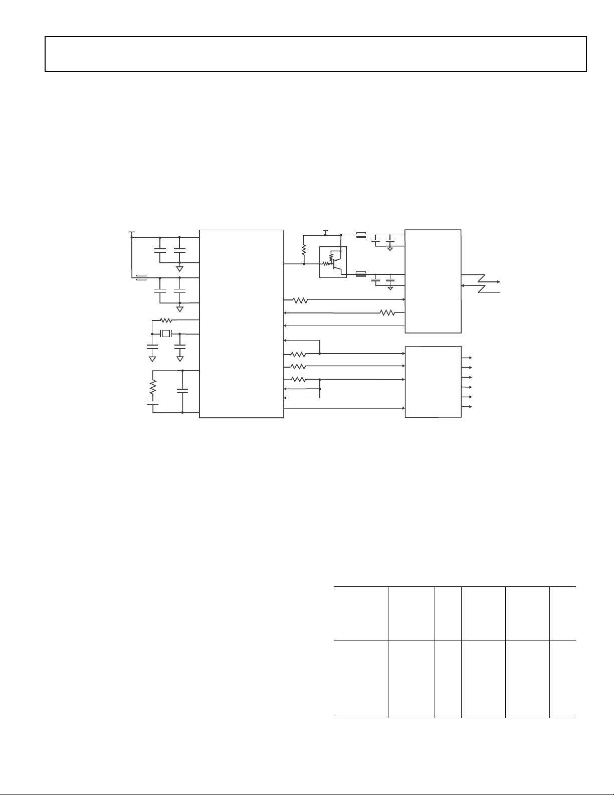
Figure 1. ADSP-BF549 Functional Block Diagram
Blackfin and the Blackfin logo are registered trademarks of Analog Devices, Inc.
Rev. D
Information furnished by Analog Devices is believed to be accurate and reliable.
However, no responsibility is assumed by Analog Devices for its use, nor for any
infringements of patents or other rights of third parties that may result from its use.
Specifications subject to change without notice. No license is granted by implication
or otherwise under any patent or patent rights of Analog Devices. Trademarks and
registered trademarks are the property of their respective owners.
One Technology Way, P.O.Box 9106, Norwood, MA 02062-9106 U.S.A.
Tel: 781.329.4700 www.analog.com
Fax: 781.461.3113 © 2011 Analog Devices, Inc. All rights reserved.

ADSP-BF542/ADSP-BF544/ADSP-BF547/ADSP-BF548/ADSP-BF549
TABLE OF CONTENTS
General Description ................................................. 3
Low Power Architecture ......................................... 4
System Integration ................................................ 4
Blackfin Processor Peripherals ................................. 4
Blackfin Processor Core .......................................... 4
Memory Architecture ............................................ 6
DMA Controllers .................................................. 9
Real-Time Clock ................................................. 10
Watchdog Timer ................................................ 10
Timers ............................................................. 10
Up/Down Counter and Thumbwheel Interface .......... 11
Serial Ports (SPORTs) .......................................... 11
Serial Peripheral Interface (SPI) Ports ...................... 11
UART Ports (UARTs) .......................................... 11
Controller Area Network (CAN) ............................ 12
TWI Controller Interface ...................................... 12
Ports ................................................................ 12
Pixel Compositor (PIXC) ...................................... 13
Enhanced Parallel Peripheral Interface (EPPI) ........... 13
USB On-the-Go Dual-Role Device Controller ............ 13
ATA/ATAPI-6 Interface ....................................... 14
Keypad Interface ................................................. 14
Secure Digital (SD)/SDIO Controller ....................... 14
Code Security ..................................................... 14
Media Transceiver MAC Layer (MXVR) ................... 14
Dynamic Power Management ................................ 15
Voltage Regulation .............................................. 16
Clock Signals ...................................................... 17
Booting Modes ................................................... 18
Instruction Set Description .................................... 21
Development Tools .............................................. 21
Designing an Emulator-Compatible Processor Board . . . 21
MXVR Board Layout Guidelines ............................. 21
Related Documents .............................................. 22
Related Signal Chains ........................................... 22
Lockbox Secure Technology Disclaimer .................... 22
Pin Descriptions .................................................... 23
Specifications ........................................................ 33
400-Ball CSP_BGA Package ...................................... 92
Outline Dimensions ................................................ 98
Surface-Mount Design .......................................... 98
Automotive Products .............................................. 99
Ordering Guide ..................................................... 99
REVISION HISTORY
5/11—Rev. C to Rev. D
Numerous small corrections and additions to document.
Major changes/additions include:
Added several extended temperature models. For more infor-
mation, see Ordering Guide ...................................... 99
Added new text for pin descriptions in Pin Descriptions .. 23
Added 400 MHz Junction Temperature to Parameter column of
the Operating Conditions table in Specifications ............ 33
Updated Table 15 to include information on extended tempera-
ture grade parts. See System Clock Requirements ........... 34
Data in the Nonautomotive 400 MHz column of Electrical
Characteristics also applies to extended temperature grade as
noted in footnote 1. See Electrical Characteristics .......... 35
Updated Table 23 to reflect RoHS compliant part is optional.
See Package Information ......................................... 40
Updated Table 31 to reflect extended temperature grade part.
See DDR SDRAM/Mobile DDR SDRAM Clock and Control
Cycle Timing ........................................................ 47
Added timer clock timing specification table (Table 47) and fig-
ure (Figure 41). See Timer Clock Timing ...................... 66
Updated package diagram to correct JEDEC specification and
outdated coplanarity number. See Outline Dimensions .... 98
To view product/process change notifications (PCNs) related to
this data sheet revision, please visit the processor's product page
on the www.analog.com website and use the View PCN link.
Rev. D | Page 2 of 100 | May 2011
ADSP-BF542/ADSP-BF544/ADSP-BF547/ADSP-BF548/ADSP-BF549
GENERAL DESCRIPTION
The ADSP-BF54x Blackfin® processors are members of the
Blackfin family of products, incorporating the Analog Devices/
Intel Micro Signal Architecture (MSA). Blackfin processors
combine a dual-MAC state-of-the-art signal processing engine,
the advantages of a clean, orthogonal RISC-like microprocessor
instruction set, and single-instruction, multiple-data (SIMD)
multimedia capabilities into a single instruction-set
architecture.
Specific performance, memory configurations, and features of
ADSP-BF54x Blackfin processors are shown in Table 1.
Table 1. ADSP-BF54x Processor Features
Processor
Features
ADSP-BF549
ADSP-BF548
ADSP-BF547
ADSP-BF544
ADSP-BF542
Lockbox® 1code security
128-bit AES/ ARC4 data encryption 11111
SD/SDIO controller 1 1 1 – 1
Pixel compositor 1 1 1 1 1
18- or 24-bit EPPI0 with LCD 1 1 1 1 –
16-bit EPPI1, 8-bit EPPI2 1 1 1 1 1
Host DMA port 1 1 1 1 –
NAND flash controller 1 1 1 1 1
ATAPI 111–1
High speed USB OTG 1 1 1 – 1
Keypad interface 1 1 1 – 1
MXVR 1 – – – –
CAN ports 2 2 – 2 1
TWI ports 22221
SPI ports 33322
UART ports 44433
SPORTs 44433
Up/down counter 11111
Timers 11 11 11 11 8
General-purpose I/O pins 152 152 152 152 152
Memory
Configura-
tions
(K Bytes)
Maximum core instruction rate (MHz) 533 533 600 533 600
1
Lockbox is a registered trademark of Analog Devices, Inc.
2
This ROM is not customer-configurable.
L1 Instruction SRAM/cache 16 16 16 16 16
L1 Instruction SRAM 48 48 48 48 48
L1 Data SRAM/cache 32 32 32 32 32
L1 Data SRAM 32 32 32 32 32
L1 Scratchpad SRAM 44444
2
L1 ROM
L2 128 128 128 64 –
L3 Boot ROM
2
11111
64 64 64 64 64
44444
Specific peripherals for ADSP-BF54x Blackfin processors are
shown in Table 2.
Table 2. Specific Peripherals for ADSP-BF54x Processors
Module
ADSP-BF549
ADSP-BF548
ADSP-BF547
ADSP-BF544
ADSP-BF542
EBIU (async) PPPPP
NAND flash controller PPPPP
ATAPI PPP–P
Host DMA port (HOSTDP) PPPP–
SD/SDIO controller P P P – P
EPPI0 PPPP–
EPPI1 PPPPP
EPPI2 PPPPP
SPORT0 PPP––
SPORT1 PPPPP
SPORT2 PPPPP
SPORT3 PPPPP
SPI0 PPPPP
SPI1 PPPPP
SPI2 PPP––
UART0 PPPPP
UART1 PPPPP
UART2 PPP––
UART3 PPPPP
High speed USB OTG PPP–P
CAN0 P P – P P
CAN1 P P – P –
TWI0 PPPPP
TWI1 PPPP–
Timer 0–7 PPPPP
Timer 8–10 PPPP–
Up/down counter PPPPP
Keypad interface P P P – P
MXVR P––––
GPIOs PPPPP
Rev. D | Page 3 of 100 | May 2011

ADSP-BF542/ADSP-BF544/ADSP-BF547/ADSP-BF548/ADSP-BF549
The ADSP-BF54x Blackfin processors are completely code- and
pin-compatible. They differ only with respect to their performance, on-chip memory, and selection of I/O peripherals.
Specific performance, memory, and feature configurations are
shown in Table 1.
By integrating a rich set of industry-leading system peripherals
and memory, Blackfin processors are the platform of choice for
next-generation applications that require RISC-like programmability, multimedia support, and leading-edge signal
processing in one integrated package.
LOW POWER ARCHITECTURE
Blackfin processors provide world-class power management
and performance. Blackfin processors are designed in a low
power and low voltage design methodology and feature on-chip
dynamic power management, the ability to vary both the voltage
and frequency of operation to significantly lower overall power
consumption. Reducing both voltage and frequency can result
in a substantial reduction in power consumption as compared
to reducing only the frequency of operation. This translates into
longer battery life for portable appliances.
SYSTEM INTEGRATION
The ADSP-BF54x Blackfin processors are highly integrated
system-on-a-chip solutions for the next generation of embedded network connected applications. By combining industrystandard interfaces with a high performance signal processing
core, users can develop cost-effective solutions quickly without
the need for costly external components. The system peripherals
include a high speed USB OTG (On-the-Go) controller with
integrated PHY, CAN 2.0B controllers, TWI controllers, UART
ports, SPI ports, serial ports (SPORTs), ATAPI controller,
SD/SDIO controller, a real-time clock, a watchdog timer, LCD
controller, and multiple enhanced parallel peripheral interfaces.
BLACKFIN PROCESSOR PERIPHERALS
The ADSP-BF54x processors contain a rich set of peripherals
connected to the core via several high bandwidth buses, providing flexibility in system configuration as well as excellent overall
system performance (see Figure 1 on Page 1). The generalpurpose peripherals include functions such as UARTs, SPI,
TWI, timers with pulse width modulation (PWM) and pulse
measurement capability, general-purpose I/O pins, a real-time
clock, and a watchdog timer. This set of functions satisfies a
wide variety of typical system support needs and is augmented
by the system expansion capabilities of the part. The ADSPBF54x processors contain dedicated network communication
modules and high speed serial and parallel ports, an interrupt
controller for flexible management of interrupts from the onchip peripherals or external sources, and power management
control functions to tailor the performance and power characteristics of the processor and system to many application
scenarios.
All of the peripherals, except for general-purpose I/O, CAN,
TWI, real-time clock, and timers, are supported by a flexible
DMA structure. There are also separate memory DMA channels
dedicated to data transfers between the processor's various
memory spaces, including external DDR (either standard or
mobile, depending on the device) and asynchronous memory.
Multiple on-chip buses running at up to 133 MHz provide
enough bandwidth to keep the processor core running along
with activity on all of the on-chip and external peripherals.
The ADSP-BF54x Blackfin processors include an on-chip voltage regulator in support of the dynamic power management
capability. The voltage regulator provides a range of core voltage levels when supplied from V
be bypassed at the user’s discretion.
. The voltage regulator can
DDEXT
BLACKFIN PROCESSOR CORE
As shown in Figure 2 on Page 5, the Blackfin processor core
contains two 16-bit multipliers, two 40-bit accumulators, two
40-bit ALUs, four video ALUs, and a 40-bit shifter. The computation units process 8-, 16-, or 32-bit data from the register file.
The compute register file contains eight 32-bit registers. When
performing compute operations on 16-bit operand data, the
register file operates as 16 independent 16-bit registers. All
operands for compute operations come from the multiported
register file and instruction constant fields.
Each MAC can perform a 16-bit by 16-bit multiply in each
cycle, accumulating the results into the 40-bit accumulators.
Signed and unsigned formats, rounding, and saturation are
supported.
The ALUs perform a traditional set of arithmetic and logical
operations on 16- or 32-bit data. In addition, many special
instructions are included to accelerate various signal processing
tasks. These include bit operations such as field extract and population count, modulo 2
and rounding, and sign/exponent detection. The set of video
instructions include byte alignment and packing operations,
16-bit and 8-bit adds with clipping, 8-bit average operations,
and 8-bit subtract/absolute value/accumulate (SAA) operations.
Also provided are the compare/select and vector search
instructions.
For certain instructions, two 16-bit ALU operations can be performed simultaneously on register pairs (a 16-bit high half and
16-bit low half of a compute register). By also using the second
ALU, quad 16-bit operations are possible.
The 40-bit shifter can perform shifts and rotates and is used to
support normalization, field extract, and field deposit
instructions.
The program sequencer controls the flow of instruction execution, including instruction alignment and decoding. For
program flow control, the sequencer supports PC relative and
indirect conditional jumps (with static branch prediction), and
subroutine calls. Hardware is provided to support zero-overhead looping. The architecture is fully interlocked, meaning that
the programmer need not manage the pipeline when executing
instructions with data dependencies.
The address arithmetic unit provides two addresses for simultaneous dual fetches from memory. It contains a multiported
register file consisting of four sets of 32-bit index, modify,
32
multiply, divide primitives, saturation
Rev. D | Page 4 of 100 | May 2011
ADSP-BF542/ADSP-BF544/ADSP-BF547/ADSP-BF548/ADSP-BF549
SEQUENCER
ALIGN
DECODE
LOOP BUFFER
16
16
8888
40 40
A0 A1
BARREL
SHIFTER
DATA ARITHMETIC UNIT
CONTROL
UNIT
R7.H
R6.H
R5.H
R4.H
R3.H
R2.H
R1.H
R0.H
R7.L
R6.L
R5.L
R4.L
R3.L
R2.L
R1.L
R0.L
ASTAT
40 40
32
32
32
32
32
32
32LD0
LD1
SD
DAG0
DAG1
ADDRESS ARITHMETIC UNIT
I3
I2
I1
I0
L3
L2
L1
L0
B3
B2
B1
B0
M3
M2
M1
M0
SP
FP
P5
P4
P3
P2
P1
P0
DA1
DA0
32
32
32
PREG
RAB
32
TO MEMORY
length, and base registers (for circular buffering), and eight
additional 32-bit pointer registers (for C-style indexed stack
manipulation).
Blackfin processors support a modified Harvard architecture in
combination with a hierarchical memory structure. Level 1 (L1)
memories are those that typically operate at the full processor
speed with little or no latency. At the L1 level, the instruction
memory holds instructions only. The two data memories hold
data, and a dedicated scratchpad data memory stores stack and
local variable information.
In addition, multiple L1 memory blocks are provided, offering a
configurable mix of SRAM and cache. The memory management unit (MMU) provides memory protection for individual
tasks that may be operating on the core and can protect system
registers from unintended access.
The architecture provides three modes of operation: user mode,
supervisor mode, and emulation mode. User mode has
restricted access to certain system resources, thus providing a
protected software environment, while supervisor mode has
unrestricted access to the system and core resources.
The Blackfin processor instruction set has been optimized so
that 16-bit opcodes represent the most frequently used instructions, resulting in excellent compiled code density. Complex
DSP instructions are encoded into 32-bit opcodes, representing
fully featured multifunction instructions. Blackfin processors
support a limited multi-issue capability, where a 32-bit instruction can be issued in parallel with two 16-bit instructions,
allowing the programmer to use many of the core resources in a
single instruction cycle.
The Blackfin processor assembly language uses an algebraic syntax for ease of coding and readability. The architecture has been
optimized for use in conjunction with the C/C++ compiler,
resulting in fast and efficient software implementations.
Figure 2. Blackfin Processor Core
Rev. D | Page 5 of 100 | May 2011

ADSP-BF542/ADSP-BF544/ADSP-BF547/ADSP-BF548/ADSP-BF549
RESERVED
CORE MMR REGISTERS (2M BYTES)
RESERVED
SCRATCHPAD SRAM (4K BYTES)
INSTRUCTION BANK B SRAM (16K BYTES)
SYSTEM MMR REGISTERS (2M BYTES)
RESERVED
RESERVED
DATA BANK B SRAM / CACHE (16K BYTES)
DATA BANK B SRAM (16K BYTES)
DATA BANK A SRAM / CACHE (16K BYTES)
ASYNC MEMORY BANK 3 (64M BYTES)
ASYNC MEMORY BANK 2 (64M BYTES)
ASYNC MEMORY BANK 1 (64M BYTES)
ASYNC MEMORY BANK 0 (64M BYTES)
DDR MEM BANK 0 (8M BYTES to 256M BYTES)
INSTRUCTION SRAM / CACHE (16K BYTES)
INTERNAL MEMORY MAPEXTERNAL MEMORY MAP
FFFF FFFF
FEB0 0000
FFB0 0000
FFA2 4000
FFA1 0000
FF90 8000
FF90 4000
FF80 8000
FF80 4000
3000 0000
2C00 0000
2800 0000
2400 0000
2000 0000
EF00 0000
0000 0000
FFC0 0000
FFB0 1000
FFA0 0000
DATA BANK A SRAM (16K BYTES)
FF90 0000
FF80 0000
RESERVED
RESERVED
C000
FFA0 8000
INSTRUCTION BANK A SRAM (32K BYTES)
RESERVED
BOOT ROM (4K BYTES)
EF00 1000
FFE0 0000
FEB2 0000
FFA1 4000
L1 ROM (64K BYTE)
L2 SRAM (128K BYTES)
DDR MEM BANK 1 (8M BYTES to 256M BYTES)
RESERVED
TOP OF LAST
DDR PAGE
RESERVED
FFA0
0x
0x
0x
0x
0x
0x
0x
0x
0x
0x
0x
0x
0x
0x
0x
0x
0x
0x
0
x
0x
0x
0x
0x
0x
0x
0x
0x
MEMORY ARCHITECTURE
The ADSP-BF54x processors view memory as a single unified
4G byte address space, using 32-bit addresses. All resources,
including internal memory, external memory, and I/O control
registers, occupy separate sections of this common address
space. The memory portions of this address space are arranged
in a hierarchical structure to provide a good cost/performance
balance of some very fast, low-latency on-chip memory as cache
or SRAM, and larger, lower-cost and performance off-chip
memory systems. See Figure 3 on Page 6.
The on-chip L1 memory system is the highest-performance
memory available to the Blackfin processor. The off-chip memory system, accessed through the external bus interface unit
(EBIU), provides expansion with flash memory, SRAM, and
double-rate SDRAM (standard or mobile DDR), optionally
accessing up to 768M bytes of physical memory.
Most of the ADSP-BF54x Blackfin processors also include an L2
SRAM memory array which provides up to 128K bytes of high
speed SRAM, operating at one half the frequency of the core and
with slightly longer latency than the L1 memory banks (for
information on L2 memory in each processor, see Table 1). The
L2 memory is a unified instruction and data memory and can
hold any mixture of code and data required by the system
design. The Blackfin cores share a dedicated low latency 64-bit
data path port into the L2 SRAM memory.
The memory DMA controllers (DMAC1 and DMAC0) provide
high-bandwidth data-movement capability. They can perform
block transfers of code or data between the internal memory
and the external memory spaces.
Internal (On-Chip) Memory
The ADSP-BF54x processors have several blocks of on-chip
memory providing high bandwidth access to the core.
The first block is the L1 instruction memory, consisting of
64K bytes of SRAM, of which 16K bytes can be configured as a
four-way set-associative cache or as SRAM. This memory is
accessed at full processor speed.
The second on-chip memory block is the L1 data memory, consisting of 64K bytes of SRAM, of which 32K bytes can be
configured as a two-way set-associative cache or as SRAM. This
memory block is accessed at full processor speed.
The third memory block is a 4K byte scratchpad SRAM, which
runs at the same speed as the L1 memories. It is only accessible
as data SRAM and cannot be configured as cache memory.
The fourth memory block is the factory programmed L1
instruction ROM, operating at full processor speed. This ROM
is not customer-configurable.
The fifth memory block is the L2 SRAM, providing up to 128K
bytes of unified instruction and data memory, operating at one
half the frequency of the core.
Finally, there is a 4K byte boot ROM connected as L3 memory.
It operates at full SCLK rate.
1
For ADSP-BF544 processors, L2 SRAM is 64K Bytes
(0xFEB0000–0xFEB0FFFF). For ADSP-BF542 processors, there is no L2
SRAM.
External (Off-Chip) Memory
Through the external bus interface unit (EBIU), the
ADSP-BF54x Blackfin processors provide glueless connectivity
to external 16-bit wide memories, such as DDR and mobile
DDR SDRAM, SRAM, NOR flash, NAND flash, and FIFO
devices. To provide the best performance, the bus system of the
DDR and mobile DDR interface is completely separate from the
other parallel interfaces. Furthermore, the DDR controller supports either standard DDR memory or mobile DDR memory.
See the Ordering Guide on Page 99 for details. Throughout this
document, references to “DDR” are intended to cover both the
standard and mobile DDR standards.
Rev. D | Page 6 of 100 | May 2011
Figure 3. ADSP-BF547/ADSP-BF548/ADSP-BF549
Internal/External Memory Map
1

ADSP-BF542/ADSP-BF544/ADSP-BF547/ADSP-BF548/ADSP-BF549
The DDR memory controller can gluelessly manage up to two
banks of double-rate synchronous dynamic memory (DDR and
mobile DDR SDRAM). The 16-bit interface operates at the
SCLK frequency, enabling a maximum throughput of 532M
bytes/s. The DDR and mobile DDR controller is augmented
with a queuing mechanism that performs efficient bursts into
the DDR and mobile DDR. The controller is an industry standard DDR and mobile DDR SDRAM controller with each bank
supporting from 64M bit to 512M bit device sizes and 4-, 8-, or
16-bit widths. The controller supports up to 256M bytes per
external bank. With 2 external banks, the controller supports up
to 512M bytes total. Each bank is independently programmable
and is contiguous with adjacent banks regardless of the sizes of
the different banks or their placement.
Traditional 16-bit asynchronous memories, such as SRAM,
EPROM, and flash devices, can be connected to one of the four
64M byte asynchronous memory banks, represented by four
memory select strobes. Alternatively, these strobes can function
as bank-specific read or write strobes preventing further glue
logic when connecting to asynchronous FIFO devices. See the
Ordering Guide on Page 99 for a list of specific products that
provide support for DDR memory.
In addition, the external bus can connect to advanced flash
device technologies, such as:
• Page-mode NOR flash devices
• Synchronous burst-mode NOR flash devices
•NAND flash devices
Customers should consult the Ordering Guide when selecting a
specific ADSP-BF54x component for the intended application.
Products that provide support for mobile DDR memory are
noted in the ordering guide footnotes.
NAND Flash Controller (NFC)
The ADSP-BF54x Blackfin processors provide a NAND Flash
Controller (NFC) as part of the external bus interface. NAND
flash devices provide high-density, low-cost memory. However,
NAND flash devices also have long random access times, invalid
blocks, and lower reliability over device lifetimes. Because of
this, NAND flash is often used for read-only code storage. In
this case, all DSP code can be stored in NAND flash and then
transferred to a faster memory (such as DDR or SRAM) before
execution. Another common use of NAND flash is for storage
of multimedia files or other large data segments. In this case, a
software file system may be used to manage reading and writing
of the NAND flash device. The file system selects memory segments for storage with the goal of avoiding bad blocks and
equally distributing memory accesses across all address locations. Hardware features of the NFC include:
• Support for page program, page read, and block erase of
NAND flash devices, with accesses aligned to page
boundaries.
• Error checking and correction (ECC) hardware that facilitates error detection and correction.
• A single 8-bit or 16-bit external bus interface for commands, addresses, and data.
• Support for SLC (single level cell) NAND flash devices
unlimited in size, with page sizes of 256 bytes and 512
bytes. Larger page sizes can be supported in software.
• The ability to release external bus interface pins during
long accesses.
• Support for internal bus requests of 16 bits or 32 bits.
• A DMA engine to transfer data between internal memory
and a NAND flash device.
One-Time-Programmable Memory
The ADSP-BF54x Blackfin processors have 64K bits of onetime-programmable (OTP) non-volatile memory that can be
programmed by the developer only one time. It includes the
array and logic to support read access and programming. Additionally, its pages can be write protected.
OTP enables developers to store both public and private data
on-chip. In addition to storing public and private key data for
applications requiring security, it also allows developers to store
completely user-definable data such as a customer ID, product
ID, or a MAC address. By using this feature, generic parts can be
shipped, which are then programmed and protected by the
developer within this non-volatile memory. The OTP memory
can be accessed through an API provided by the on-chip ROM.
I/O Memory Space
The ADSP-BF54x Blackfin processors do not define a separate
I/O space. All resources are mapped through the flat 32-bit
address space. On-chip I/O devices have their control registers
mapped into memory-mapped registers (MMRs) at addresses
near the top of the 4G byte address space. These are separated
into two smaller blocks, one containing the control MMRs for
all core functions and the other containing the registers needed
for setup and control of the on-chip peripherals outside of the
core. The MMRs are accessible only in supervisor mode and
appear as reserved space to on-chip peripherals.
Booting
The ADSP-BF54x Blackfin processors contain a small on-chip
boot kernel, which configures the appropriate peripheral for
booting. If the ADSP-BF54x Blackfin processors are configured
to boot from boot ROM memory space, the processor starts executing from the on-chip boot ROM. For more information, see
Booting Modes on Page 18.
Event Handling
The event controller on the ADSP-BF54x Blackfin processors
handles all asynchronous and synchronous events to the processors. The ADSP-BF54x Blackfin processors provide event
handling that supports both nesting and prioritization. Nesting
allows multiple event service routines to be active simultaneously. Prioritization ensures that servicing of a higher-priority
event takes precedence over servicing of a lower-priority event.
Rev. D | Page 7 of 100 | May 2011

ADSP-BF542/ADSP-BF544/ADSP-BF547/ADSP-BF548/ADSP-BF549
The controller provides support for five different types of
events:
• Emulation. An emulation event causes the processor to
enter emulation mode, allowing command and control of
the processor via the JTAG interface.
• Reset. This event resets the processor.
• Non-maskable interrupt (NMI). The NMI event can be
generated by the software watchdog timer or by the NMI
input signal to the processor. The NMI event is frequently
used as a power-down indicator to initiate an orderly shutdown of the system.
• Exceptions. Events that occur synchronously to program
flow (that is, the exception is taken before the instruction is
allowed to complete). Conditions such as data alignment
violations and undefined instructions cause exceptions.
• Interrupts. Events that occur asynchronously to program
flow. They are caused by input pins, timers, and other
peripherals, as well as by an explicit software instruction.
Each event type has an associated register to hold the return
address and an associated return-from-event instruction. When
an event is triggered, the state of the processor is saved on the
supervisor stack.
The ADSP-BF54x Blackfin processor event controller consists
of two stages, the core event controller (CEC) and the system
interrupt controller (SIC). The core event controller works with
the system interrupt controller to prioritize and control all system events. Conceptually, interrupts from the peripherals enter
into the SIC and are then routed directly into the general-purpose interrupts of the CEC.
Core Event Controller (CEC)
The CEC supports nine general-purpose interrupts (IVG15– 7),
in addition to the dedicated interrupt and exception events. Of
these general-purpose interrupts, the two lowest-priority interrupts (IVG15– 14) are recommended to be reserved for software
interrupt handlers, leaving seven prioritized interrupt inputs to
support the peripherals of the ADSP-BF54x Blackfin processors.
Table 3 describes the inputs to the CEC, identifies their names
in the event vector table (EVT), and lists their priorities.
System Interrupt Controller (SIC)
The system interrupt controller provides the mapping and routing of events from the many peripheral interrupt sources to the
prioritized general-purpose interrupt inputs of the CEC.
Although the ADSP-BF54x Blackfin processors provide a
default mapping, the user can alter the mappings and priorities
of interrupt events by writing the appropriate values into the
interrupt assignment registers (SIC_IARx). The ADSP-BF54x
Hardware Reference Manual, “System Interrupts” chapter
describes the inputs into the SIC and the default mappings into
the CEC.
Table 3. Core Event Controller (CEC)
Priority
(0 is Highest) Event Class EVT Entry
0Emulation/Test ControlEMU
1 Reset RST
2 Nonmaskable Interrupt NMI
3ExceptionEVX
4 Reserved —
5 Hardware Error IVHW
6 Core Timer IVTMR
7 General Interrupt 7 IVG7
8 General Interrupt 8 IVG8
9 General Interrupt 9 IVG9
10 General Interrupt 10 IVG10
11 General Interrupt 11 IVG11
12 General Interrupt 12 IVG12
13 General Interrupt 13 IVG13
14 General Interrupt 14 IVG14
15 General Interrupt 15 IVG15
Event Control
The ADSP-BF54x Blackfin processors provide the user with a
very flexible mechanism to control the processing of events. In
the CEC, three registers are used to coordinate and control
events. Each register is 16 bits wide:
• CEC interrupt latch register (ILAT). The ILAT register
indicates when events have been latched. The appropriate
bit is set when the processor has latched the event and
cleared when the event has been accepted into the system.
This register is updated automatically by the controller, but
it may be written only when its corresponding IMASK bit
is cleared.
• CEC interrupt mask register (IMASK). The IMASK register controls the masking and unmasking of individual
events. When a bit is set in the IMASK register, that event is
unmasked and is processed by the CEC when asserted. A
cleared bit in the IMASK register masks the event, preventing the processor from servicing the event even though the
event may be latched in the ILAT register. This register
may be read or written while in supervisor mode. Note that
general-purpose interrupts can be globally enabled and disabled with the STI and CLI instructions, respectively.
• CEC interrupt pending register (IPEND). The IPEND register keeps track of all nested events. A set bit in the IPEND
register indicates that the event is currently active or nested
at some level. This register is updated automatically by the
controller but may be read while in supervisor mode.
The SIC allows further control of event processing by providing
three 32-bit interrupt control and status registers. Each register
contains a bit corresponding to each of the peripheral interrupt
events shown in the ADSP-BF54x Hardware Reference Manual,
“System Interrupts” chapter.
Rev. D | Page 8 of 100 | May 2011

ADSP-BF542/ADSP-BF544/ADSP-BF547/ADSP-BF548/ADSP-BF549
• SIC interrupt mask registers (SIC_IMASKx). These registers control the masking and unmasking of each peripheral
interrupt event. When a bit is set in a register, that peripheral event is unmasked and is processed by the system
when asserted. A cleared bit in the register masks the
peripheral event, preventing the processor from servicing
the event.
• SIC interrupt status registers (SIC_ISRx). As multiple
peripherals can be mapped to a single event, these registers
allow the software to determine which peripheral event
source triggered the interrupt. A set bit indicates the
peripheral is asserting the interrupt, and a cleared bit indicates the peripheral is not asserting the event.
• SIC interrupt wakeup enable registers (SIC_IWRx). By
enabling the corresponding bit in this register, a peripheral
can be configured to wake up the processor, should the
core be idled or in Sleep mode when the event is generated.
(For more information, see Dynamic Power Management
on Page 15.)
Because multiple interrupt sources can map to a single generalpurpose interrupt, multiple pulse assertions can occur simultaneously, before or during interrupt processing for an interrupt
event already detected on this interrupt input. The IPEND register contents are monitored by the SIC as the interrupt
acknowledgement.
The appropriate ILAT register bit is set when an interrupt rising
edge is detected. (Detection requires two core clock cycles.) The
bit is cleared when the respective IPEND register bit is set. The
IPEND bit indicates that the event has entered into the processor pipeline. At this point the CEC recognizes and queues the
next rising edge event on the corresponding event input. The
minimum latency from the rising edge transition of the generalpurpose interrupt to the IPEND output asserted is three core
clock cycles; however, the latency can be much higher, depending on the activity within and the state of the processor.
DMA CONTROLLERS
ADSP-BF54x Blackfin processors have multiple, independent
DMA channels that support automated data transfers with minimal overhead for the processor core. DMA transfers can occur
between the ADSP-BF54x processors’ internal memories and
any of the DMA-capable peripherals. Additionally, DMA transfers can be accomplished between any of the DMA-capable
peripherals and external devices connected to the external
memory interfaces, including DDR and asynchronous memory
controllers.
While the USB controller and MXVR have their own dedicated
DMA controllers, the other on-chip peripherals are managed by
two centralized DMA controllers, called DMAC1 (32-bit) and
DMAC0 (16-bit). Both operate in the SC LK domain. Ea ch DMA
controller manages 12 independent peripheral DMA channels,
as well as two independent memory DMA streams. The
DMAC1 controller masters high-bandwidth peripherals over a
dedicated 32-bit DMA access bus (DAB32). Similarly, the
DMAC0 controller masters most serial interfaces over the 16-bit
DAB16 bus. Individual DMA channels have fixed access priority on the DAB buses. DMA priority of peripherals is managed
by a flexible peripheral-to-DMA channel assignment scheme.
All four DMA controllers use the same 32-bit DCB bus to
exchange data with L1 memory. This includes L1 ROM, but
excludes scratchpad memory. Fine granulation of L1 memory
and special DMA buffers minimize potential memory conflicts
when the L1 memory is accessed simultaneously by the core.
Similarly, there are dedicated DMA buses between the external
bus interface unit (EBIU) and the three DMA controllers
(DMAC1, DMAC0, and USB) that arbitrate DMA accesses to
external memories and the boot ROM.
The ADSP-BF54x Blackfin processors’ DMA controllers support both 1-dimensional (1D) and 2-dimensional (2D) DMA
transfers. DMA transfer initialization can be implemented from
registers or from sets of parameters called descriptor blocks.
The 2D DMA capability supports arbitrary row and column
sizes up to 64K elements by 64K elements, and arbitrary row
and column step sizes up to ±32K elements. Furthermore, the
column step size can be less than the row step size, allowing
implementation of interleaved data streams. This feature is
especially useful in video applications where data can be deinterleaved on the fly.
Examples of DMA types supported by the ADSP-BF54x Blackfin processors’ DMA controllers include:
• A single, linear buffer that stops upon completion
• A circular, auto-refreshing buffer that interrupts on each
full or fractionally full buffer
• 1D or 2D DMA using a linked list of descriptors
• 2D DMA using an array of descriptors, specifying only the
base DMA address within a common page
In addition to the dedicated peripheral DMA channels, the
DMAC1 and DMAC0 controllers each feature two memory
DMA channel pairs for transfers between the various memories
of the ADSP-BF54x Blackfin processors. This enables transfers
of blocks of data between any of the memories—including
external DDR, ROM, SRAM, and flash memory—with minimal
processor intervention. Like peripheral DMAs, memory DMA
transfers can be controlled by a very flexible descriptor-based
methodology or by a standard register-based autobuffer
mechanism.
The memory DMA channels of the DMAC1 controller
(MDMA2 and MDMA3) can be controlled optionally by the
external DMA request input pins. When used in conjunction
with the External Bus Interface Unit (EBIU), this handshaked
memory DMA (HMDMA) scheme can be used to efficiently
exchange data with block-buffered or FIFO-style devices connected externally. Users can select whether the DMA request
pins control the source or the destination side of the memory
DMA. It allows control of the number of data transfers for
memory DMA. The number of transfers per edge is programmable. This feature can be programmed to allow memory DMA
to have an increased priority on the external bus relative to the
core.
Rev. D | Page 9 of 100 | May 2011
ADSP-BF542/ADSP-BF544/ADSP-BF547/ADSP-BF548/ADSP-BF549
RTXO
C1 C2
X1
SUGGESTED COMP ONENTS:
ECLIPTEK EC38J (THROUGH-HOLE PACKAGE )
EPSON MC405 12 pF LOAD (SURFACE-MOUNT PACKAGE)
C1 = 22 pF
C2 = 22 pF
R1 = 10 MΩ
NOTE: C1 AND C2 ARE SPECIFIC TO CRYSTAL SPECIFIED FOR X1.
CONTACT CRYSTAL MANUFACTURER FOR DETAI LS. C1 AND C2
SPECIFICATIONS ASSUME BOARD TRACE C APACITANCE OF 3 pF.
RTXI
R1
Host DMA Port Interface
The host DMA port (HOSTDP) facilitates a host device external
to the ADSP-BF54x Blackfin processors to be a DMA master
and transfer data back and forth. The host device always masters
the transactions, and the processor is always a DMA slave
device.
The HOSTDP is enabled through the peripheral access bus.
Once the port has been enabled, the transactions are controlled
by the external host. The external host programs standard DMA
configuration words in order to send/receive data to any valid
internal or external memory location. The host DMA port controller includes the following features:
• Allows an external master to configure DMA read/write
data transfers and read port status
• Uses a flexible asynchronous memory protocol for its
external interface
• Allows an 8- or 16-bit external data interface to the host
device
• Supports half-duplex operation
• Supports little/big endian data transfers
• Acknowledge mode allows flow control on host
transactions
• Interrupt mode guarantees a burst of FIFO depth host
transactions
REAL-TIME CLOCK
The ADSP-BF54x Blackfin processors’ real-time clock (RTC)
provides a robust set of digital watch features, including current
time, stopwatch, and alarm. The RTC is clocked by a 32.768 kHz
crystal external to the ADSP-BF54x Blackfin processors. The
RTC peripheral has dedicated power supply pins so that it can
remain powered up and clocked even when the rest of the processor is in a low-power state. The RTC provides several
programmable interrupt options, including interrupt per second, minute, hour, or day clock ticks, interrupt on
programmable stopwatch countdown, or interrupt at a programmed alarm time.
The 32.768 kHz input clock frequency is divided down to a 1 Hz
signal by a prescaler. The counter function of the timer consists
of four counters: a 60-second counter, a 60-minute counter, a
24-hour counter, and a 32,768-day counter.
When enabled, the alarm function generates an interrupt when
the output of the timer matches the programmed value in the
alarm control register. There are two alarms. The first alarm is
for a time of day. The second alarm is for a day and time of
that day.
The stopwatch function counts down from a programmed value
with one-second resolution. When the stopwatch is enabled and
the counter underflows, an interrupt is generated.
Like the other peripherals, the RTC can wake up the
ADSP-BF54x processor from sleep mode upon generation of
any RTC wakeup event. Additionally, an RTC wakeup event can
wake up the ADSP-BF54x processors from deep sleep mode,
and it can wake up the on-chip internal voltage regulator from
the hibernate state.
Connect RTC pins RTXI and RTXO with external components
as shown in Figure 4.
WATCHDOG TIMER
The ADSP-BF54x processors include a 32-bit timer that can be
used to implement a software watchdog function. A software
watchdog can improve system reliability by forcing the processor to a known state through generation of a hardware reset,
non-maskable interrupt (NMI), or general-purpose interrupt if
the timer expires before being reset by software. The programmer initializes the count value of the timer, enables the
appropriate interrupt, and then enables the timer. Thereafter,
the software must reload the counter before it counts to zero
from the programmed value. This protects the system from
remaining in an unknown state where software, which would
normally reset the timer, has stopped running due to an external
noise condition or software error.
If configured to generate a hardware reset, the watchdog timer
resets both the core and the ADSP-BF54x processors’ peripherals. After a reset, software can determine if the watchdog was the
source of the hardware reset by interrogating a status bit in the
watchdog timer control register.
The timer is clocked by the system clock (SCLK) at a maximum
frequency of f
TIMERS
There are up to two timer units in the ADSP-BF54x Blackfin
processors. One unit provides eight general-purpose programmable timers, and the other unit provides three. Each timer has
an external pin that can be configured either as a pulse width
modulator (PWM) or timer output, as an input to clock the
timer, or as a mechanism for measuring pulse widths and periods of external events. These timers can be synchronized to an
external clock input on the TMRx pins, an external clock
TMRCLK input pin, or to the internal SCLK.
Rev. D | Page 10 of 100 | May 2011
Figure 4. External Components for RTC
.
SCLK

ADSP-BF542/ADSP-BF544/ADSP-BF547/ADSP-BF548/ADSP-BF549
SPI Clock Rate
f
SCLK
2 SPI_BAUD×
----------------------------------- -
=
The timer units can be used in conjunction with the four
UARTs and the CAN controllers to measure the width of the
pulses in the data stream to provide a software auto-baud detect
function for the respective serial channels.
The timers can generate interrupts to the processor core, providing periodic events for synchronization to either the system
clock or to a count of external signals.
In addition to the general-purpose programmable timers,
another timer is also provided by the processor core. This extra
timer is clocked by the internal processor clock and is typically
used as a system tick clock for generation of periodic operating
system interrupts.
UP/DOWN COUNTER AND THUMBWHEEL INTERFACE
A 32-bit up/down counter is provided that can sense the 2-bit
quadrature or binary codes typically emitted by industrial drives
or manual thumb wheels. The counter can also operate in
general-purpose up/down count modes. Then count direction is
either controlled by a level-sensitive input pin or by two edge
detectors.
A third input can provide flexible zero marker support and can
alternatively be used to input the push-button signal of thumb
wheels. All three pins have a programmable debouncing circuit.
An internal signal forwarded to the timer unit enables one timer
to measure the intervals between count events. Boundary registers enable auto-zero operation or simple system warning by
interrupts when programmable count values are exceeded.
SERIAL PORTS (SPORTS)
The ADSP-BF54x Blackfin processors incorporate up to four
dual-channel synchronous serial ports (SPORT0, SPORT1,
SPORT2, and SPORT3) for serial and multiprocessor communications. The SPORTs support the following features:
2
S capable operation.
•I
• Bidirectional operation. Each SPORT has two sets of independent transmit and receive pins, enabling up to eight
channels of I
• Buffered (8-deep) transmit and receive ports. Each port has
a data register for transferring data words to and from
other processor components and shift registers for shifting
data in and out of the data registers.
• Clocking. Each transmit and receive port can either use an
external serial clock or generate its own, in frequencies
ranging from (f
• Word length. Each SPORT supports serial data words from
3 to 32 bits in length, transferred most-significant-bit first
or least-significant-bit first.
• Framing. Each transmit and receive port can run with or
without frame sync signals for each data word. Frame sync
signals can be generated internally or externally, active high
or low, and with either of two pulse widths and early or late
frame sync.
2
S stereo audio.
/131,070) Hz to (f
SCLK
SCLK
/2) Hz.
• Companding in hardware. Each SPORT can perform
A-law or µ-law companding according to ITU recommendation G.711. Companding can be selected on the transmit
and/or receive channel of the SPORT without additional
latencies.
•DMA operations with single-cycle overhead. Each SPORT
can receive and transmit multiple buffers of memory data
automatically. The processor can link or chain sequences of
DMA transfers between a SPORT and memory.
• Interrupts. Each transmit and receive port generates an
interrupt upon completing the transfer of a data word or
after transferring an entire data buffer or buffers through
DMA.
• Multichannel capability. Each SPORT supports 128 channels out of a 1024-channel window and is compatible with
the H.100, H.110, MVIP-90, and HMVIP standards.
SERIAL PERIPHERAL INTERFACE (SPI) PORTS
The ADSP-BF54x Blackfin processors have up to three SPIcompatible ports that allow the processor to communicate with
multiple SPI-compatible devices.
Each SPI port uses three pins for transferring data: two data pins
(master output slave input, SPIxMOSI, and master input-slave
output, SPIxMISO) and a clock pin (serial clock, SPIxSCK). An
SPI chip select input pin (SPIxSS
the processor, and three SPI chip select output pins per SPI port
SPIxSELy
select pins are reconfigured general-purpose I/O pins. Using
these pins, the SPI ports provide a full-duplex, synchronous
serial interface, which supports both master/slave modes and
multimaster environments.
The SPI port’s baud rate and clock phase/polarities are programmable, and it has an integrated DMA controller,
configurable to support transmit or receive data streams. The
SPI’s DMA controller can only service unidirectional accesses at
any given time.
The SPI port’s clock rate is calculated as
Where the 16-bit SPI_BAUD register contains a value of
2 to 65,535.
During transfers, the SPI port transmits and receives simultaneously by serially shifting data in and out on its two serial data
lines. The serial clock line synchronizes the shifting and sampling of data on the two serial data lines.
let the processor select other SPI devices. The SPI
) lets other SPI devices select
UART PORTS (UARTS)
The ADSP-BF54x Blackfin processors provide up to four fullduplex universal asynchronous receiver/transmitter (UART)
ports. Each UART port provides a simplified UART interface to
other peripherals or hosts, supporting full-duplex, DMA-supported, asynchronous transfers of serial data. A UART port
Rev. D | Page 11 of 100 | May 2011

ADSP-BF542/ADSP-BF544/ADSP-BF547/ADSP-BF548/ADSP-BF549
UART Clock Rate
f
SCLK
16
1EDBO–()
UART_Divisor×
----------------------------------------------------------------------------- -
=
includes support for five to eight data bits, one or two stop bits,
and none, even, or odd parity. Each UART port supports two
modes of operation:
• PIO (programmed I/O). The processor sends or receives
data by writing or reading I/O-mapped UART registers.
The data is double-buffered on both transmit and receive.
• DMA (direct memory access). The DMA controller transfers both transmit and receive data. This reduces the
number and frequency of interrupts required to transfer
data to and from memory. Each UART has two dedicated
DMA channels, one for transmit and one for receive. These
DMA channels have lower default priority than most DMA
channels because of their relatively low service rates. Flexible interrupt timing options are available on the transmit
side.
Each UART port’s baud rate, serial data format, error code generation and status, and interrupts are programmable:
• Supporting bit rates ranging from (f
(f
) bits per second.
SCLK
• Supporting data formats from seven to 12 bits per frame.
• Both transmit and receive operations can be configured to
generate maskable interrupts to the processor.
The UART port’s clock rate is calculated as
/1,048,576) to
SCLK
The ADSP-BF54x Blackfin processors’ CAN controllers offer
the following features:
• 32 mailboxes (8 receive only, 8 transmit only, 16 configurable for receive or transmit).
• Dedicated acceptance masks for each mailbox.
• Additional data filtering on first two bytes.
• Support for both the standard (11-bit) and extended (29bit) identifier (ID) message formats.
• Support for remote frames.
• Active or passive network support.
• CAN wakeup from hibernation mode (lowest static power
consumption mode).
•Interrupts, including: TX complete, RX complete, error
and global.
The electrical characteristics of each network connection are
very demanding, so the CAN interface is typically divided into
two parts: a controller and a transceiver. This allows a single
controller to support different drivers and CAN networks. The
ADSP-BF54x Blackfin processors’ CAN module represents only
the controller part of the interface. The controller interface supports connection to 3.3 V high speed, fault-tolerant, single-wire
transceivers.
An additional crystal is not required to supply the CAN clock, as
the CAN clock is derived from the processor system clock
(SCLK) through a programmable divider.
Where the 16-bit UART divisor comes from the UARTx_DLH
register (most significant 8 bits) and UARTx_DLL register (least
significant eight bits), and the EDBO is a bit in the
UARTx_GCTL register.
In conjunction with the general-purpose timer functions, autobaud detection is supported.
UART1 and UART3 feature a pair of UARTxRTS
send) and UARTxCTS
purposes. The transmitter hardware is automatically prevented
from sending further data when the UARTxCTS
asserted. The receiver can automatically de-assert its
UARTxRTS
certain high-water level. The capabilities of the UARTs are further extended with support for the Infrared Data Association
(IrDA®) Serial Infrared Physical Layer Link Specification (SIR)
protocol.
output when the enhanced receive FIFO exceeds a
(clear to send) signals for hardware flow
(request to
input is de-
CONTROLLER AREA NETWORK (CAN)
The ADSP-BF54x Blackfin processors offer up to two CAN controllers that are communication controllers that implement the
controller area network (CAN) 2.0B (active) protocol. This protocol is an asynchronous communications protocol used in both
industrial and automotive control systems. The CAN protocol is
well suited for control applications due to its capability to communicate reliably over a network since the protocol
incorporates CRC checking, message error tracking, and fault
node confinement.
TWI CONTROLLER INTERFACE
The ADSP-BF54x Blackfin processors include up to two 2-wire
interface (TWI) modules for providing a simple exchange
method of control data between multiple devices. The modules
are compatible with the widely used I
modules offer the capabilities of simultaneous master and slave
operation and support for both 7-bit addressing and multimedia data arbitration. Each TWI interface uses two pins for
transferring clock (SCLx) and data (SDAx), and supports the
protocol at speeds up to 400K bits/sec. The TWI interface pins
are compatible with 5 V logic levels.
Additionally, the ADSP-BF54x Blackfin processors’ TWI modules are fully compatible with serial camera control bus (SCCB)
functionality for easier control of various CMOS camera sensor
devices.
2
C bus standard. The TWI
PORTS
Because of their rich set of peripherals, the ADSP-BF54x
Blackfin processors group the many peripheral signals to ten
ports—referred to as Port A to Port J. Most ports contain 16
pins, though some have fewer. Many of the associated pins are
shared by multiple signals. The ports function as multiplexer
controls. Every port has its own set of memory-mapped registers to control port muxing and GPIO functionality.
Rev. D | Page 12 of 100 | May 2011

ADSP-BF542/ADSP-BF544/ADSP-BF547/ADSP-BF548/ADSP-BF549
General-Purpose I/O (GPIO)
Every pin in Port A to Port J can function as a GPIO pin, resulting in a GPIO pin count up to 154. While it is unlikely that all
GPIO pins will be used in an application, as all pins have multiple functions, the richness of GPIO functionality guarantees
unrestrictive pin usage. Every pin that is not used by any function can be configured in GPIO mode on an individual basis.
After reset, all pins are in GPIO mode by default. Since neither
GPIO output nor input drivers are active by default, unused
pins can be left unconnected. GPIO data and direction control
registers provide flexible write-one-to-set and write-one-toclear mechanisms so that independent software threads do not
need to protect against each other because of expensive readmodify-write operations when accessing the same port.
Pin Interrupts
Every port pin on ADSP-BF54x Blackfin processors can request
interrupts in either an edge-sensitive or a level-sensitive manner
with programmable polarity. Interrupt functionality is decoupled from GPIO operation. Four system-level interrupt
channels (PINT0, PINT1, PINT2 and PINT3) are reserved for
this purpose. Each of these interrupt channels can manage up to
32 interrupt pins. The assignment from pin to interrupt is not
performed on a pin-by-pin basis. Rather, groups of eight pins
(half ports) can be flexibly assigned to interrupt channels.
Every pin interrupt channel features a special set of 32-bit memory-mapped registers that enables half-port assignment and
interrupt management. This not only includes masking, identification, and clearing of requests, it also enables access to the
respective pin states and use of the interrupt latches regardless
of whether the interrupt is masked or not. Most control registers
feature multiple MMR address entries to write-one-to-set or
write-one-to-clear them individually.
PIXEL COMPOSITOR (PIXC)
The pixel compositor (PIXC) provides image overlays with
transparent-color support, alpha blending, and color space conversion capabilities for output to TFT LCDs and NTSC/PAL
video encoders. It provides all of the control to allow two data
streams from two separate data buffers to be combined,
blended, and converted into appropriate forms for both LCD
panels and digital video outputs. The main image buffer provides the basic background image, which is presented in the
data stream. The overlay image buffer allows the user to add
multiple foreground text, graphics, or video objects on top of
the main image or video data stream.
ENHANCED PARALLEL PERIPHERAL INTERFACE (EPPI)
The ADSP-BF54x Blackfin processors provide up to three
enhanced parallel peripheral interfaces (EPPIs), supporting data
widths up to 24 bits. The EPPI supports direct connection to
TFT LCD panels, parallel analog-to-digital and digital-to-analog converters, video encoders and decoders, image sensor
modules and other general-purpose peripherals.
The following features are supported in the EPPI module:
• Programmable data length: 8 bits, 10 bits, 12 bits, 14 bits,
16 bits, 18 bits, and 24 bits per clock.
• Bidirectional and half-duplex port.
• Clock can be provided externally or can be generated
internally.
• Various framed and non-framed operating modes. Frame
syncs can be generated internally or can be supplied by an
external device.
•Various general-purpose modes with zero to three frame
syncs for both receive and transmit directions.
• ITU-656 status word error detection and correction for
ITU-656 receive modes.
• ITU-656 preamble and status word decode.
• Three different modes for ITU-656 receive modes: active
video only, vertical blanking only, and entire field mode.
• Horizontal and vertical windowing for GP 2 and 3 frame
sync modes.
• Optional packing and unpacking of data to/from 32 bits
from/to 8, 16 and 24 bits. If packing/unpacking is enabled,
endianness can be changed to change the order of packing/unpacking of bytes/words.
• Optional sign extension or zero fill for receive modes.
• During receive modes, alternate even or odd data samples
can be filtered out.
• Programmable clipping of data values for 8-bit transmit
modes.
• RGB888 can be converted to RGB666 or RGB565 for transmit modes.
• Various de-interleaving/interleaving modes for receiving/transmitting 4:2:2 YCrCb data.
• FIFO watermarks and urgent DMA features.
• Clock gating by an external device asserting the clock gating control signal.
•Configurable LCD data enable (DEN) output available on
Frame Sync 3.
USB ON-THE-GO DUAL-ROLE DEVICE CONTROLLER
The USB OTG dual-role device controller (USBDRC) provides
a low-cost connectivity solution for consumer mobile devices
such as cell phones, digital still cameras, and MP3 players,
allowing these devices to transfer data using a point-to-point
USB connection without the need for a PC host. The USBDRC
module can operate in a traditional USB peripheral-only mode
as well as the host mode presented in the On-the-Go (OTG)
supplement to the USB 2.0 specification. In host mode, the USB
module supports transfers at high speed (480 Mbps), full speed
(12 Mbps), and low speed (1.5 Mbps) rates. Peripheral-only
mode supports the high and full speed transfer rates.
Rev. D | Page 13 of 100 | May 2011

ADSP-BF542/ADSP-BF544/ADSP-BF547/ADSP-BF548/ADSP-BF549
The USB clock (USB_XI) is provided through a dedicated external crystal or crystal oscillator. See Table 62 for related timing
requirements. If using a fundamental mode crystal to provide
the USB clock, connect the crystal between USB_XI and
USB_XO with a circuit similar to that shown in Figure 7. Use a
parallel-resonant, fundamental mode, microprocessor-grade
crystal. If a third-overtone crystal is used, follow the circuit
guidelines outlined in Clock Signals on Page 17 for third-overtone crystals.
The USB On-the-Go dual-role device controller includes a
Phase Locked Loop with programmable multipliers to generate
the necessary internal clocking frequency for USB. The multiplier value should be programmed based on the USB_XI clock
frequency to achieve the necessary 480 MHz internal clock for
USB high speed operation. For example, for a USB_XI crystal
frequency of 24 MHz, the USB_PLLOSC_CTRL register should
be programmed with a multiplier value of 20 to generate a 480
MHz internal clock.
ATA/ATAPI-6 INTERFACE
The ATAPI interface connects to CD/DVD and HDD drives
and is ATAPI-6 compliant. The controller implements the
peripheral I/O mode, the multi-DMA mode, and the Ultra
DMA mode. The DMA modes enable faster data transfer and
reduced host management. The ATAPI controller supports
PIO, multi-DMA, and ultra DMA ATAPI accesses. Key features
include:
• Supports PIO modes 0, 1, 2, 3, 4
• Supports multiword DMA modes 0, 1, 2
• Supports ultra DMA modes 0, 1, 2, 3, 4, 5 (up to UDMA
100)
• Programmable timing for ATA interface unit
• Supports CompactFlash cards using true IDE mode
By default, the ATAPI_A0-2 address signals and the
ATAPI_D0-15 data signals are shared on the asynchronous
memory interface with the asynchronous memory and NAND
flash controllers. The data and address signals can be remapped
to GPIO ports F and G, respectively, by setting
PORTF_MUX[1:0] to b#01.
KEYPAD INTERFACE
The keypad interface is a 16-pin interface module that is used to
detect the key pressed in a 8 × 8 (maximum) keypad matrix. The
size of the input keypad matrix is programmable. The interface
is capable of filtering the bounce on the input pins, which is
common in keypad applications. The width of the filtered
bounce is programmable. The module is capable of generating
an interrupt request to the core once it identifies that any key
has been pressed.
The interface supports a press-release-press mode and infrastructure for a press-hold mode. The former mode identifies a
press, release and press of a key as two consecutive presses of the
same key, whereas the latter mode checks the input key’s state in
periodic intervals to determine the number of times the same
key is meant to be pressed. It is possible to detect when multiple
keys are pressed simultaneously and to provide limited key resolution capability when this happens.
SECURE DIGITAL (SD)/SDIO CONTROLLER
The SD/SDIO controller is a serial interface that stores data at a
data rate of up to 10M bytes per second using a 4-bit data line.
The SD/SDIO controller supports the SD memory mode only.
The interface supports all the power modes and performs error
checking by CRC.
CODE SECURITY
An OTP/security system, consisting of a blend of hardware and
software, provides customers with a flexible and rich set of code
security features with Lockbox
include:
• OTP memory
• Unique chip ID
• Code authentication
• Secure mode of operation
The security scheme is based upon the concept of authentication of digital signatures using standards-based algorithms and
provides a secure processing environment in which to execute
code and protect assets. See Lockbox Secure Technology Dis-
claimer on Page 22.
®
secure technology. Key features
MEDIA TRANSCEIVER MAC LAYER (MXVR)
The ADSP-BF549 Blackfin processors provide a media transceiver (MXVR) MAC layer, allowing the processor to be
connected directly to a MOST
Figure 5 on Page 15 for an example of a MXVR MOST
connection.
The MXVR is fully compatible with industry-standard standalone MOST controller devices, supporting 22.579 Mbps or
24.576 Mbps data transfer. It offers faster lock times, greater jitter immunity, and a sophisticated DMA scheme for data
transfers. The high speed internal interface to the core and L1
memory allows the full bandwidth of the network to be utilized.
The MXVR can operate as either the network master or as a network slave.
The MXVR supports synchronous data, asynchronous packets,
and control messages using dedicated DMA channels that operate autonomously from the processor core moving data to and
from L1 and/or L2 memory. Synchronous data is transferred to
or from the synchronous data physical channels on the MOST
bus through eight programmable DMA channels. The synchronous data DMA channels can operate in various modes
including modes that trigger DMA operation when data patterns are detected in the receive data stream. Furthermore, two
DMA channels support asynchronous traffic, and two others
support control message traffic.
1
MOST is a registered trademark of Standard Microsystems, Corp.
®
1 network through an FOT. See
Rev. D | Page 14 of 100 | May 2011
ADSP-BF542/ADSP-BF544/ADSP-BF547/ADSP-BF548/ADSP-BF549
Interrupts are generated when a user-defined amount of synchronous data has been sent or received by the processor or
when asynchronous packets or control messages have been sent
or received.
The MXVR peripheral can wake up the ADSP-BF549 Blackfin
processor from sleep mode when a wakeup preamble is received
over the network or based on any other MXVR interrupt event.
Additionally, detection of network activity by the MXVR can be
used to wake up the ADSP-BF549 Blackfin processor from the
hibernate state. These features allow the ADSP-BF549 processor
1.25V
R1
330 6
C1
0.047
2% PPS
600Z
0.01
1%
MF
MF
C2
330pF
2% PPS
0.1 MF
24.576MHz
VDDINT
GND
VDDMP
GNDMP
MXO
MXI
MLF_P
MLF_M
ADSP-BF549
PG11/MTXON
PH5/MTX
PH6/MRX
PH7/MRXON
PC4/RFS0
MFS
PC1/MMCLK
PC5/MBCLK
PC3/TSCLK0
PC7/RSCLK0
PC2/DT0PRI
10k 6
33
336
33 6
27 6
to operate in a low-power state when there is no network activity or when data is not currently being received or transmitted
by the MXVR.
The MXVR clock is provided through a dedicated external crystal or crystal oscillator. The frequency of the external crystal or
crystal oscillator can be 256 Fs, 384 Fs, 512 Fs, or 1024 Fs for
Fs = 38 kHz, 44.1 kHz, or 48 kHz. If using a crystal to provide
the MXVR clock, use a parallel-resonant, fundamental mode,
microprocessor-grade crystal.
5.0V
XN4114
6
600Z
600Z
MOST FOT
RXVCC
RXGND
MOST
TXVCC
TXGND
TX_DATA
0 6
RX_DATA
STATUS
AUDIO DAC
L/RCLK
MCLK
BCLK
SD ATA
NETWORK
AUDIO
CHANNELS
Figure 5. MXVR MOST Connection
DYNAMIC POWER MANAGEMENT
The ADSP-BF54x Blackfin processors provide five operating
modes, each with a different performance/power profile. In
addition, dynamic power management provides the control
functions to dynamically alter the processor core supply voltage,
further reducing power dissipation. Control of clocking to each
of the ADSP-BF54x Blackfin processors’ peripherals also
reduces power consumption. See Table 4 for a summary of the
power settings for each mode.
Full-On Operating Mode—Maximum Performance
In the full-on mode, the PLL is enabled and is not bypassed,
providing the capability to run at the maximum operational frequency. This is the power-up default execution state in which
maximum performance can be achieved. The processor core
and all enabled peripherals run at full speed.
Active Operating Mode—Moderate Power Savings
In the active mode, the PLL is enabled but bypassed. Because the
PLL is bypassed, the processor’s core clock (CCLK) and system
clock (SCLK) run at the input clock (CLKIN) frequency. DMA
access is available to appropriately configured L1 memories.
In the active mode, it is possible to disable the control input to
the PLL by setting the PLL_OFF bit in the PLL control register.
This register can be accessed with a user-callable routine in the
on-chip ROM called bfrom_SysControl(). For more information, see the “Dynamic Power Management” chapter in the
ADSP-BF54x Blackfin Processor Hardware Reference. If disabled, the PLL must be re-enabled before transitioning to the
full-on or sleep modes.
Table 4. Power Settings
Mode/State
PLL
PLL
Bypassed
Core
Clock
(CCLK)
System
Clock
(SCLK)
Core
Full On Enabled No Enabled Enabled On
Active Enabled/
Ye s E na bl ed E na bl e d O n
Disabled
Sleep Enabled - Disabled Enabled On
Deep Sleep Disabled - Disabled Disabled On
Hibernate Disabled - Disabled Disabled Off
Power
Rev. D | Page 15 of 100 | May 2011

ADSP-BF542/ADSP-BF544/ADSP-BF547/ADSP-BF548/ADSP-BF549
Sleep Operating Mode—High Dynamic Power Savings
The sleep mode reduces dynamic power dissipation by disabling
the clock to the processor core (CCLK). The PLL and system
clock (SCLK), however, continue to operate in this mode. Typically an external event or RTC activity will wake up the
processor. In the sleep mode, assertion of a wakeup event
enabled in the SIC_IWRx register causes the processor to sense
the value of the BYPASS bit in the PLL control register
(PLL_CTL). If BYPASS is disabled, the processor transitions to
the full on mode. If BYPASS is enabled, the processor transitions to the active mode.
In the sleep mode, system DMA access to L1 memory is not
supported.
Deep Sleep Operating Mode—Maximum Dynamic Power Savings
The deep sleep mode maximizes dynamic power savings by disabling the clocks to the processor core (CCLK) and to all
synchronous peripherals (SCLK). Asynchronous peripherals,
such as the RTC, may still be running but will not be able to
access internal resources or external memory. This
powered-down mode can only be exited by assertion of the reset
interrupt (RESET
) or by an asynchronous interrupt generated
by the RTC. In deep sleep mode, an asynchronous RTC interrupt causes the processor to transition to the active mode.
Assertion of RESET
while in deep sleep mode causes the proces-
sor to transition to the full on mode.
Hibernate State—Maximum Static Power Savings
The hibernate state maximizes static power savings by disabling
the voltage and clocks to the processor core (CCLK) and to all
the synchronous peripherals (SCLK). The internal voltage regulator for the processor can be shut off by using the
bfrom_SysControl() function in the on-chip ROM. This sets the
internal power supply voltage (V
) to 0 V to provide the
DDINT
greatest power savings mode. Any critical information stored
internally (memory contents, register contents, and so on) must
be written to a non-volatile storage device prior to removing
power if the processor state is to be preserved.
Since V
is still supplied in this mode, all of the external
DDEXT
pins three-state, unless otherwise specified. This allows other
devices that may be connected to the processor to have power
still applied without drawing unwanted current.
The internal supply regulator can be woken up by CAN, by the
MXVR, by the keypad, by the up/down counter, by the USB,
and by some GPIO pins. It can also be woken up by a real-time
clock wakeup event or by asserting the RESET
pin. Waking up
from hibernate state initiates the hardware reset sequence.
With the exception of the VR_CTL and the RTC registers, all
internal registers and memories lose their content in hibernate
state. State variables may be held in external SRAM or DDR
memory.
Power Domains
As shown in Table 5, the ADSP-BF54x Blackfin processors support different power domains. The use of multiple power
domains maximizes flexibility while maintaining compliance
with industry standards and conventions. By isolating the internal logic of the ADSP-BF54x Blackfin processors into its own
power domain separate from the RTC and other I/O, the processors can take advantage of dynamic power management
without affecting the RTC or other I/O devices. There are no
sequencing requirements for the various power domains.
Table 5. Power Domains
Power Domain VDD Range
All internal logic, except RTC, DDR, and USB V
RTC internal logic and crystal I/O V
DDR external memory supply V
USB internal logic and crystal I/O V
Internal voltage regulator V
MXVR PLL and logic V
All other I/O V
DDINT
DDRTC
DDDDR
DDUSB
DDVR
DDMP
DDEXT
VOLTAGE REGULATION
The ADSP-BF54x Blackfin processors provide an on-chip voltage regulator that can generate processor core voltage levels
from an external supply (see specifications in Operating Condi-
tions on Page 33). Figure 6 on Page 17 shows the typical
external components required to complete the power management system. The regulator controls the internal logic voltage
levels and is programmable with the voltage regulator control
register (VR_CTL) in increments of 50 mV. This register can be
accessed using the bfrom_SysControl() function in the on-chip
ROM. To reduce standby power consumption, the internal voltage regulator can be programmed to remove power to the
processor core while keeping I/O power supplied. While in
hibernate state, V
still be applied, eliminating the need for external buffers. The
voltage regulator can be activated from this power-down state
by assertion of the RESET
sequence. The regulator can also be disabled and bypassed at the
user’s discretion. For all 600 MHz speed grade models and all
automotive grade models, the internal voltage regulator must
not be used and V
information regarding design of the voltage regulator circuit,
see Switching Regulator Design Considerations for the ADSP-
BF533 Blackfin Processors (EE-228).
, V
DDEXT
DDRTC
pin, which then initiates a boot
must be tied to V
DDVR
, V
DDDDR
, V
DDUSB
. For additional
DDEXT
, and V
DDVR
can
Rev. D | Page 16 of 100 | May 2011
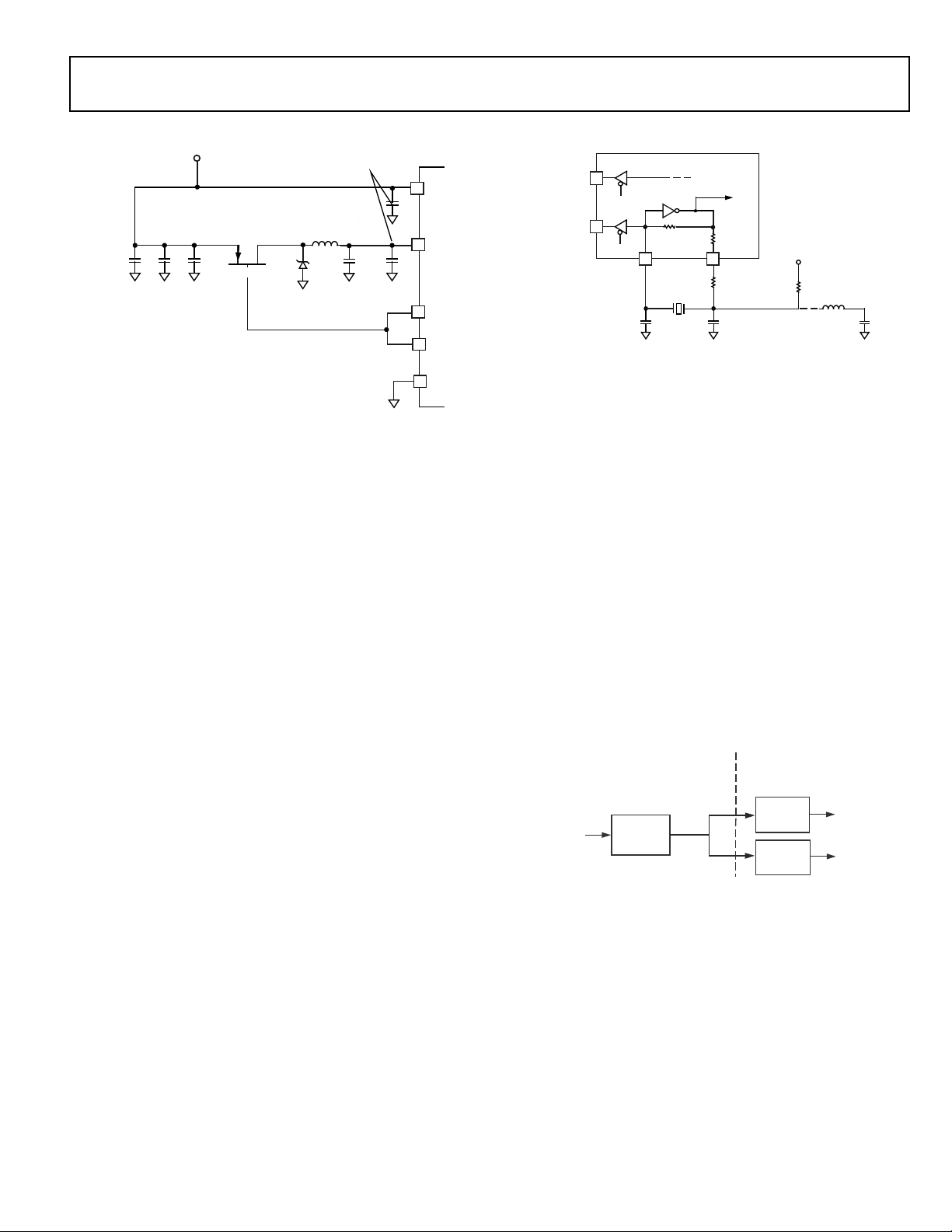
ADSP-BF542/ADSP-BF544/ADSP-BF547/ADSP-BF548/ADSP-BF549
V
DDVR
(LOW-INDUCTANCE)
V
DDINT
VR
OUT
100μF
VR
OUT
GND
SHORT AND LOW-
INDUCTANCE WIRE
V
DDVR
+
+
100μF
10μF
LOW ESR
100nF
SETOFDECOUPLING
CAPACITORS
FDS9431A
ZHCS1000
2.7V TO 3.6V
INPUT VOLTAGE
RANGE
NOTE: DESIGNER SHOULD MINIMIZE
TRACE LENGTH TO FDS9431A.
10μH
CLKIN
CLKOUT
XTAL
EN
CLKBUF
TO PLL CIRC UITRY
FROVERTONE
OPERAOTION ONLY
NOTE: VALUES MARKED WITH * MUST BE CUSTOMIZED
DEPENDING ON THE CRYSTAL AND LAYOUT. PLEASE
ANALYZE CAREFULLY.
18 pF*
EN
18 pF*
7000
BLACKFIN
0
*
V
DDEXT
1M
PLL
0.5x - 64x
1:15
1, 2, 4, 8
VCO
CLKIN
DYNAMIC MODIFICATION
REQUIRES PLL SEQUENCING
DYNAMIC MODIFICATION
ON-THE-FLY
CCLK
SCLK
Figure 7. External Crystal Connections
Figure 6. Voltage Regulator Circuit
CLOCK SIGNALS
The ADSP-BF54x Blackfin processors can be clocked by an
external crystal, a sine wave input, or a buffered, shaped clock
derived from an external clock oscillator.
If an external clock is used, it should be a TTL-compatible signal
and must not be halted, changed, or operated below the specified frequency during normal operation. This signal is
connected to the processor’s CLKIN pin. When an external
clock is used, the XTAL pin must be left unconnected.
Alternatively, because the ADSP-BF54x Blackfin processors
include an on-chip oscillator circuit, an external crystal may be
used. For fundamental frequency operation, use the circuit
shown in Figure 7. A parallel-resonant, fundamental frequency,
microprocessor-grade crystal is connected across the CLKIN
and XTAL pins. The on-chip resistance between CLKIN and the
XTAL pin is in the 500 k range. Typically, further parallel
resistors are not recommended. The two capacitors and the
series resistor shown in Figure 7 fine-tune phase and amplitude
of the sine frequency. The 1MOhm pull-up resistor on the
XTAL pin guarantees that the clock circuit is properly held inactive when the processor is in the hibernate state.
The capacitor and resistor values shown in Figure 7 are typical
values only. The capacitor values are dependent upon the crystal
manufacturers’ load capacitance recommendations and the PCB
physical layout. The resistor value depends on the drive level
specified by the crystal manufacturer. System designs should
verify the customized values based on careful investigations on
multiple devices over temperature range.
A third-overtone crystal can be used at frequencies above
25 MHz. The circuit is then modified to ensure crystal operation
only at the third overtone by adding a tuned inductor circuit as
shown in Figure 7. A design procedure for third-overtone operation is discussed in detail in an Application Note, Using Third
Overtone Crystals (EE-168).
The Blackfin core runs at a different clock rate than the on-chip
peripherals. As shown in Figure 8 on Page 17, the core clock
(CCLK) and system peripheral clock (SCLK) are derived from
Rev. D | Page 17 of 100 | May 2011
the input clock (CLKIN) signal. An on-chip PLL is capable of
multiplying the CLKIN signal by a programmable 0.5× to 64×
multiplication factor (bounded by specified minimum and maximum VCO frequencies). The default multiplier is 8×, but it can
be modified by a software instruction sequence. This sequence
is managed by the bfrom_SysControl() function in the on-chip
ROM.
On-the-fly CCLK and SCLK frequency changes can be applied
by using the bfrom_SysControl() function in the on-chip ROM.
Whereas the maximum allowed CCLK and SCLK rates depend
on the applied voltages V
DDINT
and V
, the VCO is always
DDEXT
permitted to run up to the frequency specified by the part’s
speed grade.
The CLKOUT pin reflects the SCLK frequency to the off-chip
world. It functions as a reference for many timing specifications.
While inactive by default, it can be enabled using the
EBIU_AMGCTL register.
Note: For CCLK and SCLK specifications, see Tab le 1 5.
Figure 8. Frequency Modification Methods
All on-chip peripherals are clocked by the system clock (SCLK).
The system clock frequency is programmable by means of the
SSEL3–0 bits of the PLL_DIV register. The values programmed
into the SSEL fields define a divide ratio between the PLL output
(VCO) and the system clock. SCLK divider values are 1 through
15. Table 6 illustrates typical system clock ratios. The default
ratio is 4.

ADSP-BF542/ADSP-BF544/ADSP-BF547/ADSP-BF548/ADSP-BF549
Table 6. Example System Clock Ratios
Example Frequency Ratios
Signal Name
SSEL3–0
0010 2:1 200 100
0110 6:1 300 50
1010 10:1 500 50
Divider Ratio
VCO/SCLK
VCO SCLK
(MHz)
Note that the divisor ratio must be chosen to limit the system
clock frequency to its maximum of f
. The SSEL value can be
SCLK
dynamically changed without any PLL lock latencies by writing
the appropriate values to the PLL divisor register (PLL_DIV)
using the bfrom_SysControl() function in the on-chip ROM.
The core clock (CCLK) frequency can also be dynamically
changed by means of the CSEL1–0 bits of the PLL_DIV register.
Supported CCLK divider ratios are 1, 2, 4, and 8, as shown in
Table 7. The default ratio is 1. This programmable core clock
capability is useful for fast core frequency modifications.
The maximum CCLK frequency not only depends on the part’s
speed grade, it also depends on the applied V
voltage. See
DDINT
Table 12 on Page 34 for details.
Table 7. Core Clock Ratios
Example Frequency Ratios
Signal Name
CSEL1–0
00 1:1 300 300
01 2:1 300 150
10 4:1 500 125
11 8:1 200 25
Divider Ratio
VCO/CCLK
VCO CCLK
(MHz)
BOOTING MODES
The ADSP-BF54x Blackfin processors have many mechanisms
(listed in Table 8) for automatically loading internal and external memory after a reset. The boot mode is specified by four
BMODE input pins dedicated to this purpose. There are two
categories of boot modes: master and slave. In master boot
modes, the processor actively loads data from parallel or serial
memories. In slave boot modes, the processor receives data
from an external host device.
Table 8. Booting Modes
BMODE3–0 Description
0000 Idle-no boot
0001 Boot from 8- or 16-bit external flash memory
0010 Boot from 16-bit asynchronous FIFO
0011 Boot from serial SPI memory (EEPROM or flash)
0100 Boot from SPI host device
0101 Boot from serial TWI memory (EEPROM or flash)
0110 Boot from TWI host
0111 Boot from UART host
Table 8. Booting Modes (Continued)
BMODE3–0 Description
1000 Reserved
1001 Reserved
1010 Boot from DDR SDRAM/Mobile DDR SDRAM
1011 Boot from OTP memory
1100 Reserved
1101 Boot from 8- or 16-bit NAND flash memory via NFC
1110 Boot from 16-bit host DMA
1111 Boot from 8-bit host DMA
The boot modes listed in Table 8 provide a number of mechanisms for automatically loading the processor’s internal and
external memories after a reset. By default, all boot modes use
the slowest allowed configuration settings. Default settings can
be altered via the initialization code feature at boot time or by
proper OTP programming at pre-boot time. Some boot modes
require a boot host wait (HWAIT) signal, which is a GPIO output signal that is driven and toggled by the boot kernel at boot
time. If pulled high through an external pull-up resistor, the
HWAIT signal behaves active high and will be driven low when
the processor is ready for data. Conversely, when pulled low,
HWAIT is driven high when the processor is ready for data.
When the boot sequence completes, the HWAIT pin can be
used for other purposes. By default, HWAIT functionality is on
GPIO port B (PB11). However, if PB11 is otherwise utilized in
the system, an alternate boot host wait (HWAITA) signal can be
enabled on GPIO port H (PH7) by programming the
OTP_ALTERNATE_HWAIT bit in the PBS00L OTP
memory page.
The BMODE pins of the reset configuration register, sampled
during power-on resets and software-initiated resets, implement the following modes:
• Idle-no boot mode (BMODE = 0x0)—In this mode, the
processor goes into the idle state. The idle boot mode helps
to recover from illegal operating modes, in case the OTP
memory is misconfigured.
• Boot from 8- or 16-bit external flash memory—
(BMODE = 0x1)—In this mode, the boot kernel loads the
first block header from address 0x2000 0000 and, depending on instructions contained in the header, the boot kernel
performs an 8- or 16-bit boot or starts program execution
at the address provided by the header. By default, all configuration settings are set for the slowest device possible (3cycle hold time; 15-cycle R/W access times; 4-cycle setup).
The ARDY pin is not enabled by default. It can, however,
be enabled by OTP programming. Similarly, all interface
behavior and timings can be customized through OTP programming. This includes activation of burst-mode or pagemode operation. In this mode, all asynchronous interface
signals are enabled at the port muxing level.
Rev. D | Page 18 of 100 | May 2011

ADSP-BF542/ADSP-BF544/ADSP-BF547/ADSP-BF548/ADSP-BF549
• Boot from 16-bit asynchronous FIFO (BMODE = 0x2)—In
this mode, the boot kernel starts booting from address
0x2030 0000. Every 16-bit word that the boot kernel has to
read from the FIFO must be requested by a low pulse on
the DMAR1 pin.
• Boot from serial SPI memory, EEPROM or flash
(BMODE = 0x3)—8-, 16-, 24- or 32-bit addressable devices
are supported. The processor uses the PE4 GPIO pin to
select a single SPI EEPROM or flash device and uses SPI0
to submit a read command and successive address bytes
(0x00) until a valid 8-, 16-, 24-, or 32-bit addressable device
is detected. Pull-up resistors are required on the SPI0SEL1
and SPI0MISO pins. By default, a value of 0x85 is written to
the SPI0_BAUD register.
• Boot from SPI host device (BMODE = 0x4)—The processor operates in SPI slave mode (using SPI0) and is
configured to receive the bytes of the .LDR file from an SPI
host (master) agent. The HWAIT signal must be interrogated by the host before every transmitted byte. A pull-up
resistor is required on the SPI0SS
input. A pull-down resistor on the serial clock (SPI0SCK) may improve signal
quality and booting robustness.
• Boot from serial TWI memory, EEPROM or flash
(BMODE = 0x5)—The processor operates in master mode
(using TWI0) and selects the TWI slave with the unique ID
0xA0. The processor submits successive read commands to
the memory device starting at two-byte internal address
0x0000 and begins clocking data into the processor. The
TWI memory device should comply with Philips I
2
C Bus
Specification version 2.1 and have the capability to autoincrement its internal address counter such that the contents of the memory device can be read sequentially. By
default, a prescale value of 0xA and CLKDIV value of
0x0811 is used. Unless altered by OTP settings, an I
2
C
memory that takes two address bytes is assumed. Development tools ensure that data that is booted to memories that
cannot be accessed by the Blackfin core is written to an
intermediate storage place and then copied to the final destination via memory DMA.
• Boot from TWI host (BMODE = 0x6)—The TWI host
agent selects the slave with the unique ID 0x5F. The processor (using TWI0) replies with an acknowledgement, and
the host can then download the boot stream. The TWI host
agent should comply with Philips I
sion 2.1. An I
2
C multiplexer can be used to select one
2
C Bus Specification ver-
processor at a time when booting multiple processors from
a single TWI.
• Boot from UART host (BMODE = 0x7)—In this mode, the
processor uses UART1 as the booting source. Using an
autobaud handshake sequence, a boot-stream-formatted
program is downloaded by the host. The host agent selects
a bit rate within the UART’s clocking capabilities.
When performing the autobaud, the UART expects an “@”
(0x40) character (eight data bits, one start bit, one stop bit,
no parity bit) on the UART1RX pin to determine the bit
rate. It then replies with an acknowledgement, which is
composed of four bytes (0xBF, the value of UART1_DLL,
the value of UART1_DLH, and finally 0x00). The host can
then download the boot stream. The processor deasserts
the UART1RTS
output to hold off the host; UART1CTS
functionality is not enabled at boot time.
• Boot from (DDR) SDRAM (BMODE = 0xA)—In this
mode, the boot kernel starts booting from address
0x0000 0010. This is a warm boot scenario only. The
SDRAM is expected to contain a valid boot stream and the
SDRAM controller must have been configured by the OTP
settings.
• Boot from 8-bit and 16-bit external NAND flash memory
(BMODE = 0xD)—In this mode, auto detection of the
NAND flash device is performed. The processor configures
PORTJ GPIO pins PJ1 and PJ2 to enable the ND_CE
ND_RB
signals, respectively. For correct device operation,
pull-up resistors are required on both ND_CE
ND_RB
(PJ2) signals. By default, a value of 0x0033 is writ-
and
(PJ1) and
ten to the NFC_CTL register. The booting procedure
always starts by booting from byte 0 of block 0 of the
NAND flash device. In this boot mode, the HWAIT signal
does not toggle. The respective GPIO pin remains in the
high-impedance state.
NAND flash boot supports the following features:
• Device auto detection
• Error detection and correction for maximum
reliability
• No boot stream size limitation
• Peripheral DMA via channel 22, providing efficient
transfer of all data (excluding the ECC parity data)
• Software-configurable boot mode for booting from
boot streams expanding multiple blocks, including
bad blocks
• Software-configurable boot mode for booting from
multiple copies of the boot stream allowing for handling of bad blocks and uncorrectable errors
• Configurable timing via OTP memory
Small page NAND flash devices must have a 512-byte page
size, 32 pages per block, a 16-byte spare area size and a bus
configuration of eight bits. By default, all read requests
from the NAND flash are followed by four address cycles.
If the NAND flash device requires only three address
cycles, then the device must be capable of ignoring the
additional address cycle.
The small page NAND flash device must comply with the
following command set:
Reset: 0xFF
Read lower half of page: 0x00
Read upper half of page: 0x01
Read spare area: 0x50
Rev. D | Page 19 of 100 | May 2011

ADSP-BF542/ADSP-BF544/ADSP-BF547/ADSP-BF548/ADSP-BF549
For large page NAND flash devices, the 4-byte electronic
signature is read in order to configure the kernel for booting. This allows support for multiple large page devices.
The fourth byte of the electronic signature must comply
with the specifications in Table 9.
Any configuration from Table 9 that also complies with the
command set listed below is directly supported by the boot
kernel. There are no restrictions on the page size or block
size as imposed by the small-page boot kernel.
Table 9. Byte 4 Electronic Signature Specification
Page Size (excluding
spare area)
Spare Area Size D2 0 8 bytes/512 bytes
Block Size (excluding
spare area)
Bus Width D6 0 x8
Not Used for
Configuration
D1:D0 00 1K bytes
01 2K bytes
10 4K bytes
11 8K bytes
1 16 bytes/512 bytes
D5:4 00 64K bytes
01 128K bytes
10 256K bytes
11 512K bytes
1x16
D3, D7
Large page devices must support the following command set:
Reset: 0xFF
Read Electronic Signature: 0x90
Read: 0x00, 0x30 (confirm command)
Large page devices must not support or react to NAND flash
command 0x50. This is a small page NAND flash command
used for device auto detection.
By default, the boot kernel will always issue five address cycles;
therefore, if a large page device requires only four cycles, the
device must be capable of ignoring the additional address cycle.
16-bit NAND flash memory devices must only support the issuing of command and address cycles via the lower eight bits of
the data bus. Devices that use the full 16-bit bus for command
and address cycles are not supported.
• Boot from OTP memory (BMODE = 0xB)—This provides
a standalone booting method. The boot stream is loaded
from on-chip OTP memory. By default, the boot stream is
expected to start from OTP page 0x40 and can occupy all
public OTP memory up to page 0xDF (2560 bytes). Since
the start page is programmable, the maximum size of the
boot stream can be extended to 3072 bytes.
• Boot from 16-bit host DMA (BMODE = 0xE)—In this
mode, the host DMA port is configured in 16-bit acknowledge mode with little endian data format. Unlike other
modes, the host is responsible for interpreting the boot
stream. It writes data blocks individually into the host
DMA port. Before configuring the DMA settings for each
block, the host may either poll the ALLOW_CONFIG bit in
HOST_STATUS or wait to be interrupted by the HWAIT
signal. When using HWAIT, the host must still check
ALLOW_CONFIG at least once before beginning to configure the host DMA port. After completing the
configuration, the host is required to poll the READY bit in
HOST_STATUS before beginning to transfer data. When
the host sends an HIRQ control command, the boot kernel
issues a CALL instruction to address 0xFFA0 0000. It is the
host’s responsibility to ensure valid code has been placed at
this address. The routine at address 0xFFA0 0000 can be a
simple initialization routine to configure internal
resources, such as the SDRAM controller, which then
returns using an RTS instruction. The routine may also be
the final application, which will never return to the boot
kernel.
• Boot from 8-bit host DMA (BMODE = 0xF)—In this
mode, the host DMA port is configured in 8-bit interrupt
mode with little endian data format. Unlike other modes,
the host is responsible for interpreting the boot stream. It
writes data blocks individually to the host DMA port.
Before configuring the DMA settings for each block, the
host may either poll the ALLOW_CONFIG bit in
HOST_STATUS or wait to be interrupted by the HWAIT
signal. When using HWAIT, the host must still check
ALLOW_CONFIG at least once before beginning to configure the host DMA port. The host will receive an
interrupt from the HOST_ACK signal every time it is
allowed to send the next FIFO depth’s worth (sixteen 32-bit
words) of information. When the host sends an HIRQ control command, the boot kernel issues a CALL instruction to
address 0xFFA0 0000. It is the host's responsibility to
ensure valid code has been placed at this address. The routine at address 0xFFA0 0000 can be a simple initialization
routine to configure internal resources, such as the
SDRAM controller, which then returns using an RTS
instruction. The routine may also be the final application,
which will never return to the boot kernel.
For each of the boot modes, a 16-byte header is first read from
an external memory device. The header specifies the number of
bytes to be transferred and the memory destination address.
Multiple memory blocks may be loaded by any boot sequence.
Once all blocks are loaded, program execution commences from
the address stored in the EVT1 register.
Prior to booting, the pre-boot routine interrogates the OTP
memory. Individual boot modes can be customized or disabled
based on OTP programming. External hardware, especially
booting hosts, may monitor the HWAIT signal to determine
Rev. D | Page 20 of 100 | May 2011

ADSP-BF542/ADSP-BF544/ADSP-BF547/ADSP-BF548/ADSP-BF549
when the pre-boot has finished and the boot kernel starts the
boot process. However, the HWAIT signal does not toggle in
NAND boot mode. By programming OTP memory, the user
can instruct the preboot routine to also customize the PLL, voltage regulator, DDR controller, and/or asynchronous memory
interface controller.
The boot kernel differentiates between a regular hardware reset
and a wakeup-from-hibernate event to speed up booting in the
later case. Bits 6-4 in the system reset configuration (SYSCR)
register can be used to bypass the pre-boot routine and/or boot
kernel in case of a software reset. They can also be used to simulate a wakeup-from-hibernate boot in the software reset case.
The boot process can be further customized by “initialization
code.” This is a piece of code that is loaded and executed prior to
the regular application boot. Typically, this is used to configure
the DDR controller or to speed up booting by managing PLL,
clock frequencies, wait states, and/or serial bit rates.
The boot ROM also features C-callable function entries that can
be called by the user application at run time. This enables second-stage boot or booting management schemes to be
implemented with ease.
INSTRUCTION SET DESCRIPTION
The Blackfin processor family assembly language instruction set
employs an algebraic syntax designed for ease of coding and
readability. The instructions have been specifically tuned to provide a flexible, densely encoded instruction set that compiles to
a very small final memory size. The instruction set also provides
fully featured multifunction instructions that allow the programmer to use many of the processor core resources in a single
instruction. Coupled with many features more often seen on
microcontrollers, this instruction set is very efficient when compiling C and C++ source code. In addition, the architecture
supports both user (algorithm/application code) and supervisor
(O/S kernel, device drivers, debuggers, ISRs) modes of operation, allowing multiple levels of access to core processor
resources.
The assembly language, which takes advantage of the processor’s unique architecture, offers the following advantages:
• Seamlessly integrated DSP/MCU features are optimized for
both 8-bit and 16-bit operations.
• A multi-issue load/store modified-Harvard architecture,
which supports two 16-bit MAC or four 8-bit ALU + two
load/store + two pointer updates per cycle.
• All registers, I/O, and memory are mapped into a unified
4G byte memory space, providing a simplified programming model.
• Microcontroller features, such as arbitrary bit and bit-field
manipulation, insertion, and extraction; integer operations
on 8-, 16-, and 32-bit data-types; and separate user and
supervisor stack pointers.
• Code density enhancements, which include intermixing of
16- and 32-bit instructions (no mode switching, no code
segregation). Frequently used instructions are encoded in
16 bits.
DEVELOPMENT TOOLS
The ADSP-BF54x Blackfin processors are supported with a
complete set of CROSSCORE® software and hardware development tools, including Analog Devices emulators and
VisualDSP++® development environment. The same emulator
hardware that supports other Blackfin processors also fully
emulates the ADSP-BF54x Blackfin processors.
EZ-KIT Lite Evaluation Board
For evaluation of ADSP-BF54x Blackfin processors, use the
ADSP-BF548 EZ-KIT Lite
Devices. Order part number ADZS-BF548-EZLITE. The board
comes with on-chip emulation capabilities and is equipped to
enable software development. Multiple daughter cards are
available.
®
board available from Analog
DESIGNING AN EMULATOR-COMPATIBLE PROCESSOR BOARD
The Analog Devices family of emulators are tools that every system developer needs to test and debug hardware and software
systems. Analog Devices has supplied an IEEE 1149.1 JTAG test
access port (TAP) on each JTAG processor. The emulator uses
the TAP to access the internal features of the processor, allowing the developer to load code, set breakpoints, observe
variables, observe memory, and examine registers. The processor must be halted to send data and commands, but once an
operation has been completed by the emulator, the processor is
set running at full speed with no impact on system timing.
To use these emulators, the target board must include a header
that connects the processor’s JTAG port to the emulator.
For details on target board design issues including mechanical
layout, single processor connections, multiprocessor scan
chains, signal buffering, signal termination, and emulator pod
logic, see Analog Devices JTAG Emulation Technical Reference
(EE-68) on the Analog Devices web site under
www.analog.com/ee-notes. This document is updated regularly
to keep pace with improvements to emulator support.
MXVR BOARD LAYOUT GUIDELINES
The MXVR Loop Filter RC network is connected between the
MLF_P and MLF_M pins in the following manner:
Capacitors:
• C1: 0.047 F (PPS type, 2% tolerance recommended)
• C2: 330 pF (PPS type, 2% tolerance recommended)
Resistor:
• R1: 330 (1% tolerance)
The RC network should be located physically close to the
MLF_P and MLF_M pins on the board.
The RC network should be shielded using GND
Avoid routing other switching signals near the RC network to
avoid crosstalk.
traces.
MP
Rev. D | Page 21 of 100 | May 2011

ADSP-BF542/ADSP-BF544/ADSP-BF547/ADSP-BF548/ADSP-BF549
MXI driven with external clock oscillator IC:
• MXI should be driven with the clock output of a clock
oscillator IC running at a frequency of 49.152 MHz or
45.1584 MHz.
• MXO should be left unconnected.
• Avoid routing other switching signals near the oscillator
and clock output trace to avoid crosstalk. When not possible, shield traces with ground.
MXI/MXO with external crystal:
• The crystal must be a fundamental mode crystal running at
a frequency of 49.152 MHz or 45.1584 MHz.
• The crystal and load capacitors should be placed physically
close to the MXI and MXO pins on the board.
• Board trace capacitance on each lead should not be more
than 3 pF.
• Trace capacitance plus load capacitance should equal the
load capacitance specification for the crystal.
• Avoid routing other switching signals near the crystal and
components to avoid crosstalk. When not possible, shield
traces and components with ground.
/GNDMP—MXVR PLL power domain:
V
DDMP
•Route V
and GNDMP with wide traces or as isolated
DDMP
power planes.
•Drive V
• Place a ferrite bead between the V
V
DDMP
• Locally bypass V
capacitors to GND
• Avoid routing switching signals near to V
to same level as V
DDMP
pin for noise isolation.
with 0.1 F and 0.01 F decoupling
DDMP
.
MP
.
DDINT
power plane and the
DDINT
DDMP
and GNDMP
traces to avoid crosstalk.
Fiber optic transceiver (FOT) connections:
• Keep the traces between the ADSP-BF549 processor and
the FOT as short as possible.
• The receive data trace connecting the FOT receive data
output pin to the ADSP-BF549 PH6/MRX input pin should
have a 0 series termination resistor placed close to the
FOT receive data output pin. Typically, the edge rate of the
FOT receive data signal driven by the FOT is very slow, and
further degradation of the edge rate is not desirable.
• The transmit data trace connecting the ADSP-BF549
PH5/MTX output pin to the FOT transmit data input pin
should have a 27 series termination resistor placed close
to the ADSP-BF549 PH5/MTX pin.
• The receive data trace and the transmit data trace between
the ADSP-BF549 processor and the FOT should not be
routed close to each other in parallel over long distances to
avoid crosstalk.
RELATED DOCUMENTS
The following publications that describe the ADSP-BF54x
Blackfin processors (and related processors) can be ordered
from any Analog Devices sales office or accessed electronically
on www.analog.com:
• ADSP-BF54x Blackfin Processor Hardware Reference, Vol-
ume 1 and Volume 2
• Blackfin Processor Programming Reference
• ADSP-BF542/BF544/BF547/BF548/BF549
Blackfin Anomaly List
RELATED SIGNAL CHAINS
A signal chain is a series of signal-conditioning electronic components that receive input (data acquired from sampling either
real-time phenomena or from stored data) in tandem, with the
output of one portion of the chain supplying input to the next.
Signal chains are often used in signal processing applications to
gather and process data or to apply system controls based on
analysis of real-time phenomena. For more information about
this term and related topics, see the "signal chain" entry in
Wikipedia or the Glossary of EE Terms on the Analog Devices
website.
Analog Devices eases signal processing system development by
providing signal processing components that are designed to
work together well. A tool for viewing relationships between
specific applications and related components is available on the
www.analog.com website.
The Application Signal Chains page in the Circuits from the
TM
site (http://www.analog.com/circuits) provides:
Lab
• Graphical circuit block diagram presentation of signal
chains for a variety of circuit types and applications
• Drill down links for components in each chain to selection
guides and application information
• Reference designs applying best practice design techniques
LOCKBOX SECURE TECHNOLOGY DISCLAIMER
Analog Devices products containing Lockbox Secure Technology are warranted by Analog Devices as detailed in the Analog
Devices Standard Terms and Conditions of Sale. To our knowledge, the Lockbox secure technology, when used in accordance
with the data sheet and hardware reference manual specifications, provides a secure method of implementing code and data
safeguards. However, Analog Devices does not guarantee that
this technology provides absolute security. ACCORDINGLY,
ANALOG DEVICES HEREBY DISCLAIMS ANY AND ALL
EXPRESS AND IMPLIED WARRANTIES THAT THE LOCKBOX SECURE TECHNOLOGY CANNOT BE BREACHED,
COMPROMISED, OR OTHERWISE CIRCUMVENTED AND
IN NO EVENT SHALL ANALOG DEVICES BE LIABLE FOR
ANY LOSS, DAMAGE, DESTRUCTION, OR RELEASE OF
DATA, INFORMATION, PHYSICAL PROPERTY, OR INTELLECTUAL PROPERTY.
Rev. D | Page 22 of 100 | May 2011

ADSP-BF542/ADSP-BF544/ADSP-BF547/ADSP-BF548/ADSP-BF549
PIN DESCRIPTIONS
The ADSP-BF54x processor pin multiplexing scheme is shown
in Table 10.
Table 10. Pin Multiplexing
Primary Pin
Func tion
(Number of
1, 2
Pins)
Port A
GPIO (16 pins) SPORT2 (8 pins) TMR4 (1 pin) TACI7 (1 pin)
Port B
GPIO (15 pins) TWI1 (2 pins)
Port C
GPIO (16 pins) SPORT0 (8 pins) MXVR MMCLK, MBCLK
Port D
GPIO (16 pins) PPI1 D0–15 (16 pins) Host D0–15 (16 pins) SPORT1 (8 pins) PPI0 D18– 23 (6 pins) Interrupts (8 pins)
First Peripheral
Func tion
SPORT3 (8 pins) TMR6 (1 pin)
UART2 or 3 CTL (2 pins)
UART2 (2 pins)
UART3 (2 pins)
SPI2 SEL1-3
SPI2 (3 pins) TMR3 (1 pin) HWAIT (1 pin)
SDH (6 pins) Interrupts (8 pins)
(3 pins) TMR0–2 (3 pins)
Second Peripheral
Func tion
TMR5 (1 pin)
TMR7 (1 pin)
(2 pins)
Third Peripheral
Func tion
TACLK7–0 (8 pins)
TACI2-3 (2 pins) Interrupts (15 pins)
Fourth Peripheral
Function Interrupt Capability
Interrupts (16 pins)
Interrupts (8 pins)
3
PPI2 D0–7 (8 pins) Keypad
Row 0–3
Col 0–3 (8 pins)
Port E
GPIO (16 pins) SPI0 (7 pins) Keypad
Row 4–6
Col 4–7 (7 pins)
UART0 TX (1 pin) Keypad R7 (1 pin)
UART0 RX (1 pin)
UART0 or 1 CTL (2 pins)
PPI1 CLK,FS (3 pins)
TWI0 (2 pins)
Port F
GPIO (16 pins) PPI0 D0–15 (16 pins) ATAPI D0-15A Interrupts (8 pins)
Port G
GPIO (16 pins) PPI0 CLK,FS (3 pins)
DATA 16–17 (2 pins)
SPI1 SEL1–3
SPI1 (4 pins) MXVR MTXON
CAN0 (2 pins)
CAN1 (2 pins)
(3 pins) Host CTL (3 pins) PPI2 CLK,FS (3 pins) CZM (1 pin)
TMRCLK (1 pin) Interrupts (8 pins)
ATAPI A0-2A
(1 pin) TACI4-5 (2 pins) Interrupts (8 pins)
TACI0 (1 pin) Interrupts (8 pins)
Interrupts (8 pins)
Interrupts (8 pins)
Interrupts (8 pins)
Rev. D | Page 23 of 100 | May 2011
ADSP-BF542/ADSP-BF544/ADSP-BF547/ADSP-BF548/ADSP-BF549
Table 10. Pin Multiplexing (Continued)
Primary Pin
Func tion
(Number of
1, 2
Pins)
First Peripheral
Func tion
Port H
GPIO (14 pins) UART1 (2 pins) PPI0-1_FS3 (2 pins) TACI1 (1 pin) Interrupts (8 pins)
ATAP I _R ES ET
(1 pin) TMR8 (1 pin) PPI2_FS3 (1 pin)
HOST_ADDR (1 pin) TMR9 (1 pin) Counter Down/Gate
HOST_ACK (1 pin) TMR10 (1 pin) Counter Up/Dir
MXVR MRX, MTX,
MRXON/GPW
4
(3 pins)
Port I
GPIO (16 pins) Async Addr10–25
(16 pins)
Port J
GPIO (14 pins) Async CTL and MISC Interrupts (8 pins)
1
Port connections may be inputs or outputs after power up depending on the model and boot mode chosen.
2
All port connections always power up as inputs for some period of time and require resistive termination to a safe condition if used as outputs in the system.
3
A total of 32 interrupts at once are available from ports C through J, configurable in byte-wide blocks.
4
GPW functionality available when MXVR is not present or unused.
Second Peripheral
Func tion
Third Peripheral
Func tion
Fourth Peripheral
Function Interrupt Capability
(1 pin)
(1 pin)
DMAR 0–1 (2 pins) TACI8–10 (3 pins)
TACLK8–10 (3 pins)
HWAITA
AMC Addr 4-9 (6 pins) Interrupts (6 pins)
Interrupts (8 pins)
Interrupts (8 pins)
Interrupts (6 pins)
Pin definitions for the ADSP-BF54x processors are listed in
Table 11. In order to maintain maximum function and reduce
package size and ball count, some balls have dual, multiplexed
functions. In cases where ball function is reconfigurable, the
default state is shown in plain text, while the alternate function
is shown in italics.
All pins are three-stated during and immediately after reset,
with the exception of the external memory interface, asynchronous and synchronous memory control, and the buffered XTAL
output pin (CLKBUF). On the external memory interface, the
control and address lines are driven high, with the exception of
CLKOUT, which toggles at the system clock rate. During hibernate, all outputs are three-stated unless otherwise noted in
Table 11.
All I/O pins have their input buffers disabled with the exception
of the pins that need pull-ups or pull-downs, as noted in
Table 11.
It is strongly advised to use the available IBIS models to ensure
that a given board design meets overshoot/undershoot and signal integrity requirements.
Additionally, adding a parallel termination to CLKOUT may
prove useful in further enhancing signal integrity. Be sure to
verify overshoot/undershoot and signal integrity specifications
on actual hardware.
Rev. D | Page 24 of 100 | May 2011

ADSP-BF542/ADSP-BF544/ADSP-BF547/ADSP-BF548/ADSP-BF549
Table 11. Pin Descriptions
Driver
Pin Name I/O1Function (First/ Second/Third/Fourth)
Port A: GPIO/SPORT2–3/TMR4–7
PA 0/ TFS2 I/O GPIO / SPORT2 Transmit Frame Sync C
PA 1/ DT 2SEC /TMR4 I/O GPIO / SPORT2 Transmit Data Secondary/Timer 4 C
PA 2/ DT 2PRI I/O GPIO / SPORT2 Transmit Data Primary C
PA 3/ TSCLK2 I/O GPIO / SPORT2 Transmit Serial Clock A
PA 4/ RFS2 I/O GPIO/SPORT2 Receive Frame Sync C
PA 5/ DR2SEC/TMR5 I/O GPIO / SPORT2 Receive Data Secondary/ Timer 5 C
PA 6/ DR2PRI I/O GPIO / SPORT2 Receive Data Primary C
PA 7/ RSCLK2 /TACLK0 I/O GPIO / SPORT2 Receive Serial Clock/Alternate Input Clock 0 A
PA 8/ TFS3 /TA CL K1 I/O GPIO / SPORT3 Transmit Frame Sync/Alternate Input Clock 1 C
PA 9/ DT 3SEC /TMR6 I/O GPIO / SPORT3 Transmit Data Secondary/Timer 6 C
PA 10 / DT3 PRI /TACLK2 I/O GPIO / SPORT3 Transmit Data Primary/Alternate Input Clock 2 C
PA 11 / TSCLK3/TAC LK 3 I/O GPIO/ SPORT3 Transmit Serial Clock /Alternate Input Clock 3 A
PA 12 / RFS3/TA CLK 4 I/O GPIO/SPORT3 Receive Frame Sync/Alternate Input Clock 4 C
PA 13 /
DR3SEC/TMR7/TACLK5 I/O GPIO/SPORT3 Receive Data Secondary/Timer 7 /Alternate Input Clock 5 C
PA 14 / DR3PRI /TAC LK 6 I/O GPIO / SPORT3 Receive Data Primary/ Alternate Input Clock 6 C
PA 15 / RSCLK3/TACLK7 and TACI7 I/O GPIO/SPORT3 Receive Serial Clock/Alt Input Clock 7 and Alt Capture Input 7 A
Port B: GPIO/TWI1/UART2–3/SPI2/TMR0–3
PB0/SCL1 I/O GPIO / TWI1 Serial Clock (Open-drain output: requires a pull-up resistor.) E
PB1/SDA1 I/O GPIO/TWI1 Serial Data (Open-drain output: requires a pull-up resistor.) E
PB2/UART3RTS
PB3/UART3CTS I/O GPIO/UART3 Clear to Send A
PB4/UART2TX I/O GPIO / UART2 Transmit A
PB5/UART2RX /TA CI2 I/O GPIO / UART2 Receive /Alternate Capture Input 2 A
PB6/UART3TX I/O GPIO / UART3 Transmit A
PB7/UART3RX /TA CI3 I/O GPIO / UART3 Receive /Alternate Capture Input 3 A
PB8/SPI2SS
PB9/SPI2SEL1
PB10 SPI2SEL2
PB11/SPI2SEL3
PB12/SPI2SCK I/O GPIO / SPI2 Clock A
PB13/SPI2MOSI I/O GPIO/SPI2 Master Out Slave In C
PB14/SPI2MISO I/O GPIO/SPI2 Master In Slave Out C
/TMR0 I/O GPIO / SPI2 Slave Select Input/ Timer 0 A
/TMR1 I/O GPIO /SPI2 Slave Select Enable 1/Timer 1 A
/TMR2 I/O GPIO / SPI2 Slave Select Enable 2/ Timer 2 A
/TMR3/ HWAIT I/O GPIO / SPI2 Slave Select Enable 3/Timer 3/Boot Host Wait A
I/O GPIO / UART3 Request to Send C
Typ e
2
Rev. D | Page 25 of 100 | May 2011

ADSP-BF542/ADSP-BF544/ADSP-BF547/ADSP-BF548/ADSP-BF549
Table 11. Pin Descriptions (Continued)
Pin Name I/O1Function (First/ Second/Third/Fourth)
Port C: GPIO/ SPORT0/SD Controller/MXVR (MOST)
PC0/TFS0 I/O GPIO/ SPORT0 Transmit Frame Sync C
PC1/DT0 SEC /MMCLK I/O GPIO/SPORT0 Transmit Data Secondary/MXVR Master Clock C
PC2/DT0 PRI I/O GPIO / SPORT0 Transmit Data Primary C
PC3/TSCLK0 I/O GPIO / SPORT0 Transmit Serial Clock A
PC4/RFS0 I/O GPIO / SPORT0 Receive Frame Sync C
PC5/DR0SEC/MBCLK I/O GPIO/SPORT0 Receive Data Secondary /MXVR Bit Clock C
PC6/DR0PRI I/O GPIO /SPORT0 Receive Data Primary C
PC7/RSCLK0 I/O GPIO/SPORT0 Receive Serial Clock C
PC8/SD_D0 I/O GPIO /SD Data Bus A
PC9/SD_D1 I/O GPIO /SD Data Bus A
PC10/SD_D2 I/O GPIO / SD Data Bus A
PC11/SD_D3 I/O GPIO / SD Data Bus A
PC12/SD_CLK I/O GPIO / SD Clock Output A
PC13/SD_CMD I/O GPIO / SD Command A
Port D: GPIO /PPI0–2/SPORT 1/Keypad/Host DMA
PD0/PPI1_D0/HOST_D8 / TFS1 /PPI0_D18
PD1/PPI1_D1/HOST_D9 / DT1SEC /PPI0_D19 I/O GPIO / PPI1 Data/Host DMA /SPORT1 Transmit Data Secondary/ PPI0 Data C
PD2/PPI1_D2/HOST_D10 / DT1PRI /PPI0_D20 I/O GPIO / PPI1 Data/Host DMA/SPORT1 Transmit Data Primary/PPI0 Data C
PD3/PPI1_D3/HOST_D11 / TSCLK1/PPI0_D21 I/O GPIO / PPI1 Data/Host DMA/SPORT1 Transmit Serial Clock/ PPI0 Data A
PD4/PPI1_D4/HOST_D12 /RFS1 /PPI0_D22 I/O GPIO / PPI1 Data/Host DMA/SPORT1 Receive Frame Sync/PPI0 Data C
PD5/PPI1_D5/HOST_D13/DR1SEC /PPI0_D23 I/O GPIO /PPI1 Data /Host DMA /SPORT1 Receive Data Secondary/PPI0 Data C
PD6/PPI1_D6/HOST_D14 /DR1PRI I/O GPIO /
PD7/PPI1_D7/HOST_D15 /RSCLK1 I/O GPIO/PPI1 Data /Host DMA /SPORT1 Receive Serial Clock A
PD8/PPI1_D8/HOST_D0 / PPI2_D0/KEY_ROW0 I/O GPIO/PPI1 Data /Host DMA/PPI2 Data/Keypad Row Input A
PD9/PPI1_D9/HOST_D1 /PPI2_D1 /KEY_ROW1 I/O GPIO/ PPI1 Data/ Host DMA /PPI2 Data /Keypad Row Input A
PD10/PPI1_D10/HOST_D2 /PPI2_D2/KEY_ROW2 I/O GPIO /PPI1 Data/Host DMA /PPI2 Data/Keypad Row Input A
PD11/PPI1_D11/HOST_D3 /PPI2_D3/KEY_ROW3 I/O GPIO /PPI1 Data/Host DMA /PPI2 Data/Keypad Row Input A
PD12/PPI1_D12/HOST_D4 /PPI2_D4/KEY_COL0 I/O GPIO/ PPI1 Data /Host DMA/ PPI2 Data
PD13/PPI1_D13/HOST_D5 /PPI2_D5/KEY_COL1 I/O GPIO/ PPI1 Data /Host DMA/ PPI2 Data/Keypad Column Output A
PD14/PPI1_D14/HOST_D6 /PPI2_D6/KEY_COL2 I/O GPIO/ PPI1 Data /Host DMA /PPI2 Data /Keypad Column Output A
PD15/PPI1_D15/HOST_D7 /PPI2_D7/KEY_COL3 I/O GPIO/ PPI1 Data /Host DMA /PPI2 Data /Keypad Column Output A
I/O GPIO / PPI1 Data/Host DMA/SPORT1 Transmit Frame Sync /PPI0 Data C
PPI1 Data/Host DMA/SPORT1 Receive Data Primary C
/Keypad Column Output A
Driver
Typ e
2
Rev. D | Page 26 of 100 | May 2011

ADSP-BF542/ADSP-BF544/ADSP-BF547/ADSP-BF548/ADSP-BF549
Table 11. Pin Descriptions (Continued)
Pin Name I/O1Function (First/ Second/Third/Fourth)
Port E: GPIO/SPI0/UART0-1/PPI1/TWI0/Keypad
PE0/SPI0SCK /KEY_COL7
PE1/SPI0MISO /KEY_ROW6
PE2/SPI0MOSI /KEY_COL6 I/O GPIO / SPI0 Master Out Slave In/ Keypad Column Output C
PE3/SPI0SS
/KEY_ROW5 I/O GPIO/ SPI0 Slave Select Input/Keypad Row Input A
PE4/SPI0SEL1 /KEY_COL
PE5/SPI0SEL2 /KEY_ROW4 I/O GPIO /SPI0 Slave Select Enable 2/Keypad Row Input A
PE6/SPI0SEL3
/KEY_COL4 I/O GPIO/SPI0 Slave Select Enable 3/Keypad Column Output A
PE7/UART0TX /KEY_ROW7 I/O GPIO / UART0 Transmit /Keypad Row Input A
PE8/UART0RX /TA CI 0 I/O GPIO /UART0 Receive /Alternate Capture Input 0 A
PE9/UART1RTS
PE10/UART1CTS I/O GPIO / UART1 Clear to Send A
PE11/PPI1_CLK I/O GPIO / PPI1 Clock A
PE12/PPI1_FS1 I/O GPIO/PPI1 Frame Sync 1 A
PE13/PPI1_FS2 I/O GPIO/PPI1 Frame Sync 2 A
PE14/SCL0 I/O GPIO / TWI0 Serial Clock (Open-drain output: requires a pull-up resistor.) E
PE15/SDA0 I/O GPIO/TWI0 Serial Data (Open-drain output: requires a pull-up resistor.) E
Port F: GPIO/PPI0/Alternate ATAPI Data
PF0/PPI0_D0/ATAPI_D0A I/O GPIO /PPI0 Data/Alternate ATAPI Data A
PF1/PPI0_D1/ATAPI_D1A I/O GPIO /PPI0 Data/Alternate ATAPI Data A
PF2/PPI0_D2/ATAPI_D2A I/O GPIO /PPI0 Data/Alternate ATAPI Data A
PF3/PPI0_D3/ATAPI_D3A I/O GPIO /PPI0 Data/Alternate ATAPI Data A
PF4/PPI0_D4/ATAPI_D4A I/O GPIO /PPI0 Data/Alternate ATAPI Data A
PF5/PPI0_D5/ATAPI_D5A I/O GPIO /PPI0 Data/Alternate ATAPI Data A
PF6/PPI0_D6/ATAPI_D6A I/O GPIO /PPI0 Data/Alternate ATAPI Data A
PF7/PPI0_D7/ATAPI_D7A I/O GPIO /PPI0 Data/Alternate ATAPI Data A
PF8/PPI0_D8/ATAPI_D8A I/O GPIO /PPI0 Data/Alternate ATAPI Data A
PF9/PPI0_D9/ATAPI_D9A I/O GPIO /PPI0 Data/Alternate ATAPI Data A
PF10/PPI0_D10/ATAPI_D10A I/O GPIO /
PF11/PPI0_D11/ATAPI_D11A I/O GPIO /PPI0 Data/Alternate ATAPI Data A
PF12/PPI0_D12/ATAPI_D12A I/O GPIO /PPI0 Data/Alternate ATAPI Data A
PF13/PPI0_D13/ATAPI_D13A I/O GPIO /PPI0 Data/Alternate ATAPI Data A
PF14/PPI0_D14/ATAPI_D14A I/O GPIO /PPI0 Data/Alternate ATAPI Data A
PF15/PPI0_D15/ATAPI_D15A I/O GPIO /PPI0 Data/Alternate ATAPI Data A
3
3
3
I/O GPIO / SPI0 Clock/Keypad Column Output A
I/O GPIO / SPI0 Master In Slave Out/ Keypad Row Input C
I/O GPIO / SPI0 Slave Select Enable 1/ Keypad Column Output A
I/O GPIO / UART1 Request to Send A
PPI0 Data/Alternate ATAPI Data A
Driver
Typ e
2
Rev. D | Page 27 of 100 | May 2011

ADSP-BF542/ADSP-BF544/ADSP-BF547/ADSP-BF548/ADSP-BF549
Table 11. Pin Descriptions (Continued)
Driver
Pin Name I/O1Function (First/ Second/Third/Fourth)
Port G: GPIO /PPI0/SPI1/PPI2/Up-Down
Counter/CAN0–1/Host DMA/MXVR (MOST)/ATAPI
PG0/PPI0_CLK/TMRCLK I/O GPIO / PPI0 Clock/External Timer Reference A
PG1/PPI0_FS1 I/O GPIO / PPI0 Frame Sync 1 A
PG2/PPI0_FS2/ATA PI _A0 A I/O GPIO /PPI0 Frame Sync 2/Alternate ATAPI Address A
PG3/PPI0_D16/ATAPI_A1A I/O GPIO /PPI0 Data/Alternate ATAPI Address A
PG4/PPI0_D17/ATAPI_A2A I/O GPIO /PPI0 Data/Alternate ATAPI Address A
PG5/SPI1SEL1
/HOST_CE /PPI2_FS2 /CZM I/O GPIO / SPI1 Slave Select/Host DMA Chip Enable / PPI2 Frame Sync 2 /Counter
Zero Marker
PG6/SPI1SEL2
PG7/SPI1SEL3
/HOST_RD /PPI2_FS1 I/O GPIO/SPI1 Slave Select/ Host DMA Read/ PPI2 Frame Sync 1A
/HOST_WR /PPI2_CLK I/O GPIO/SPI1 Slave Select/Host DMA Write/PPI2 Clock A
PG8/SPI1SCK I/O GPIO/SPI1 Clock C
PG9/SPI1MISO I/O GPIO / SPI1 Master In Slave Out C
PG10/SPI1MOSI I/O GPIO / SPI1 Master Out Slave In C
PG11/SPI1SS
/MTXON I/O GPIO / SPI1 Slave Select Input/ MXVR Transmit Phy On A
PG12/CAN0TX I/O GPIO /CAN0 Transmit A
PG13/CAN0RX /TA CI4 I/O GPIO /CAN0 Receive/ Alternate Capture Input 4 A
PG14/CAN1TX I/O GPIO /CAN1 Transmit A
PG15/CAN1RX /TA CI5 I/O GPIO /CAN1 Receive/ Alternate Capture Input 5 A
Port H:
GPIO/AMC /EXTDMA/ UART1 /PPI0–2/ATA PI/Up-
Down Counter/TMR8-10/ Host DMA/MXVR (MOST)
PH0/UART1TX /PPI1_FS3_DEN I/O GPIO/UART1 Transmit /PPI1 Frame Sync 3A
PH1/UART1RX /PPI0_FS3_DEN /TA CI1 I/O GPIO/UART 1 Receive/ PPI0 Frame Sync 3/Alternate Capture Input 1 A
PH2/ATA PI _RE SE T
/TMR8/PPI2_FS3_DEN I/O GPIO/ATAPI Interface Hard Reset Signal/Timer 8 /PPI2 Frame Sync 3A
PH3/HOST_ADDR /TMR9 /CDG I/O GPIO /HOST Address/ Timer 9/Count Down and Gate A
PH4/HOST_ACK /TMR10 /CUD I/O GPIO / HOST Acknowledge/Timer 10 /Count Up and Direction A
PH5/MTX /DMAR0 /TACI8 and TACLK8 I/O GPIO/MXVR Transmit Data/Ext. DMA Request /Alt Capt. In. 8 /Alt In. Clk 8 C
PH6/MRX /DMAR1 /TACI9 and TACLK9 I/O GPIO / MXVR Receive Data/Ext. DMA Request /Alt Capt. In. 9 /Alt In. Clk 9 A
PH7/MRXON
/GPW/TACI10 and TACLK10/HWAITA
4,5
I/O GPIO / MXVR Receive Phy On /Alt Capt. In. 10 /Alt In. Clk 10/Alternate Boot
Host Wait
6
PH8/A4
PH9/A5
PH10/A6
PH11/A7
PH12/A8
PH13/A9
6
6
6
6
6
I/O GPIO / Address Bus for Async Access A
I/O GPIO / Address Bus for Async Access A
I/O GPIO / Address Bus for Async Access A
I/O GPIO / Address Bus for Async Access A
I/O GPIO / Address Bus for Async Access A
I/O GPIO / Address Bus for Async Access A
Typ e
A
A
2
Rev. D | Page 28 of 100 | May 2011

ADSP-BF542/ADSP-BF544/ADSP-BF547/ADSP-BF548/ADSP-BF549
Table 11. Pin Descriptions (Continued)
Pin Name I/O1Function (First/ Second/Third/Fourth)
Port I: GPIO/AMC
PI0/A10
PI1/A11
PI2/A12
PI3/A13
PI4/A14
PI5/A15
PI6/A16
PI7/A17
PI8/A18
PI9/A19
PI10/A20
PI11/A21
PI12/A22
PI13/A23
PI14/A24
PI15/A25/NR_CLK
Port J: GPIO/AMC/ATAP I
PJ 0 / ARDY/ WA IT I/O GPIO/ Async Ready/NOR Wait A
PJ 1 / ND_CE
PJ 2 / ND_RB I/O GPIO / NAND Ready Busy A
PJ 3 / ATAP I_ DI OR I/O GPIO/ATAPI Rea d A
PJ 4 / ATAP I_ DI OW
PJ 5 / ATAP I_ CS 0
PJ 6 / ATAP I_ CS 1
PJ 7 / ATAP I_ DM ACK
PJ 8 / ATAP I_ DM AR Q
PJ 9 / ATAPI_INTRQ I/O GPIO / Interrupt Request from the Device A
PJ 10 / ATA PI _I OR DY
PJ 11 / BR
PJ 12 / BG
PJ 13 / BGH
6
6
6
6
6
6
6
6
6
6
6
6
6
6
6
6
7
I/O GPIO / Address Bus for Async Access A
I/O GPIO / Address Bus for Async Access A
I/O GPIO / Address Bus for Async Access A
I/O GPIO / Address Bus for Async Access A
I/O GPIO / Address Bus for Async Access A
I/O GPIO / Address Bus for Async Access A
I/O GPIO / Address Bus for Async Access A
I/O GPIO / Address Bus for Async Access A
I/O GPIO / Address Bus for Async Access A
I/O GPIO / Address Bus for Async Access A
I/O GPIO / Address Bus for Async Access A
I/O GPIO / Address Bus for Async Access A
I/O GPIO / Address Bus for Async Access A
I/O GPIO / Address Bus for Async Access A
I/O GPIO / Address Bus for Async Access A
I/O GPIO / Address Bus for Async Access/ NOR clock A
I/O GPIO / NAND Chip Enable A
I/O GPIO / ATAPI Wri te A
I/O GPIO / ATAPI Chip Select/Command Block A
I/O GPIO / ATAPI Chip Select A
I/O GPIO / ATAPI DMA Acknowledge A
I/O GPIO / ATAPI DMA Request A
I/O GPIO / ATAPI Ready Handshake A
8
6
6
I/O GPIO / Bus Request A
I/O GPIO / Bus Grant A
I/O GPIO / Bus Grant Hang A
Driver
Typ e
2
Rev. D | Page 29 of 100 | May 2011

ADSP-BF542/ADSP-BF544/ADSP-BF547/ADSP-BF548/ADSP-BF549
Table 11. Pin Descriptions (Continued)
Driver
Pin Name I/O1Function (First/ Second/Third/Fourth)
DDR Memory Interface
DA0–12 O DDR Address Bus D
DBA0–1 O DDR Bank Active Strobe D
DQ0–15 I/O DDR Data Bus D
DQS0–1 I/O DDR Data Strobe D
DQM0–1 O DDR Data Mask for Reads and Writes D
DCLK0–1 O DDR Output Clock D
DCLK0–1
O DDR Complementary Output Clock D
DCS0–1 ODDR Chip Selects D
9
DCLKE
O DDR Clock Enable (Requires a pull-down if hibernate with DDR self-
refresh is used.)
DRAS O DDR Row Address Strobe D
DCAS
O DDR Column Address Strobe D
DWE ODDR Write Enable D
DDR_VREF I DDR Voltage Reference
DDR_VSSR I DDR Voltage Reference Shield (Must be connected to GND.)
Asynchronous Memory Interface
A1-3 O Address Bus for Async and ATAPI Addresses A
D0-15/ND_D0-15/ATAPI_D0-15 I/O Data Bus for Async, NAND and ATAPI Accesses A
AMS0–3
O Bank Selects (Pull high with a resistor when used as chip select. Require
pull-ups if hibernate is used.)
ABE0 /ND_CLE O Byte Enables: Data Masks for Asynchronous Access/NAND Command
Latch Enable
ABE1/ND_ALE O Byte Enables: Data Masks for Asynchronous Access/ NAND Address Latch
Enable
/NR_ADV O Output Enable /NOR Address Data Valid A
AOE
ARE
AWE
ORead Enable/NOR Output Enable A
OWrite Enable A
ATAPI Controller Pins
ATAPI_PDIAG I Determines if an 80-pin cable is connected to the host. (Pull high or low
when unused.)
High Speed USB OTG Pins
USB_DP I/O USB D+ Pin (Pull low when unused.)
USB_DM I/O USB D- Pin (Pull low when unused.)
USB_XI C Clock XTAL Input (Pull high or low when unused.)
USB_XO C Clock XTAL Output (Leave unconnected when unused.)
10
USB_ID
I USB OTG ID Pin (Pull high when unused.)
Typ e
D
A
A
A
2
Rev. D | Page 30 of 100 | May 2011

ADSP-BF542/ADSP-BF544/ADSP-BF547/ADSP-BF548/ADSP-BF549
Table 11. Pin Descriptions (Continued)
Pin Name I/O1Function (First/ Second/Third/Fourth)
USB_VBUS
USB_VREF A USB Voltage Reference (Connect to GND through a 0.1 µF capacitor or
USB_RSET A USB Resistance Set (Connect to GND through an unpopulated
MXVR (MOST) Interface
MFS O MXVR Frame Sync (Leave unconnected when unused.) C
MLF_P A MXVR Loop Filter Plus (Leave unconnected when unused.)
MLF_M A MXVR Loop Filter Minus (Leave unconnected when unused.)
MXI C MXVR Crystal Input (Pull high or low when unused.)
MXO C MXVR Crystal Output (Pull high or low when unused.)
Mode Control Pins
BMODE0–3 I Boot Mode Strap 0–3
JTAG Port Pins
TDI I JTAG Serial Data In
TDO O JTAG Serial Data Out C
TRST
TMS I JTAG Mode Select
TCK I JTAG Clock
EMU
Voltage Regulator
VR
OUT
Real Time Clock
RTXO C RTC Crystal Output (Leave unconnected when unused. Does not three-
RTXI C RTC Crystal Input (Pull high or low when unused.)
Clock (PLL) Pins
CLKIN C Clock/Crystal Input
CLKOUT O Clock Output B
XTAL C Crystal Output (If CLKBUF is enabled, does not three-state during
CLKBUF O Buffered Oscillator Output (If enabled, does not three-state during
EXT_WAKE O External Wakeup from Hibernate Output (Does not three-state during
RESET
NMI
11
I/O USB VBUS Pin (Pull high or low when unused.)
leave unconnected when not used.)
resistor pad.)
I JTAG Reset (Pull low when unused.)
O Emulation Output C
0, VR
1 O External FET/BJT Drivers (Always connect together to reduce signal
OUT
impedance.)
state during hibernate.)
hibernate.)
hibernate.)
hibernate.)
I Reset
I Non-maskable Interrupt (Pull high when unused.)
Driver
Typ e
C
A
2
Rev. D | Page 31 of 100 | May 2011

ADSP-BF542/ADSP-BF544/ADSP-BF547/ADSP-BF548/ADSP-BF549
Table 11. Pin Descriptions (Continued)
Driver
Pin Name I/O1Function (First/ Second/Third/Fourth)
Supplies
V
DDINT
V
DDEXT
V
DDDDR
V
DDUSB
V
DDRTC
V
DDVR
12
12
12
12
13
P Internal Power Supply
P External Power Supply
P External DDR Power Supply
P External USB Power Supply
P RTC Clock Supply
P Internal Voltage Regulator Power Supply (Connect to V
DDEXT
when unused.)
GND G Ground
12
V
DDMP
GND
MP
12
P MXVR PLL Power Supply. (Must be driven to same level as V
to V
when unused or when MXVR is not present.)
DDINT
DDINT
. Connect
G MXVR PLL Ground (Connect to GND when unused or when MXVR is not
present.)
1
I = Input, O = Output, P =Power, G = Ground, C = Crystal, A = Analog.
2
Refer to Table 62 on Page 86 through Table 71 on Page 87 for driver types.
3
To use the SPI memory boot, SPI0SCK should have a pulldown, SPI0MISO should have a pullup, and SPI0SEL1 is used as the CS with a pullup.
4
HWAIT/HWAITA should be pulled high or low to configure polarity. See Booting Modes on Page 18.
5
GPW functionality is available when MXVR is not present or unused.
6
This pin should not be used as GPIO if booting in mode 1.
7
This pin should always be enabled as ND_CE in software and pulled high with a resistor when using NAND flash.
8
This pin should always be enabled as BR in software and pulled high to enable asynchronous access.
9
This pin must be pulled low through a 10kOhm resistor if self-refresh mode is desired during hibernate state or deep-sleep mode.
10
If the USB is used in device mode only, the USB_ID pin should be either pulled high or left unconnected.
11
This pin is an output only during initialization of USB OTG session request pulses in peripheral mode. Therefore, host mode or OTG type A mode requires that an external
voltage source of 5 V, at 8 mA or more per the OTG specification, be applied to this pin. Other OTG modes require that this external voltage be disabled.
12
To ensure proper operation, the power pins should be driven to their specified level even if the associated peripheral is not used in the application.
13
This pin must always be connected. If the internal voltage regulator is not being used, this pin may be connected to V
VDDVR specification. For automotive grade models, the internal voltage regulator must not be used and this pin must be tied to V
. Otherwise it should be powered according to the
DDEXT
DDEXT
.
Typ e
2
Rev. D | Page 32 of 100 | May 2011

ADSP-BF542/ADSP-BF544/ADSP-BF547/ADSP-BF548/ADSP-BF549
SPECIFICATIONS
OPERATING CONDITIONS
Parameter Conditions Min Nominal Max Unit
1, 2
V
DDINT
3
V
DDEXT
V
DDUSB
V
DDMP
V
DDRTC
V
DDDDR
4
V
DDVR
V
IH
V
IHDDR
12
V
IH5V
V
IHTWI
V
IHUSB
V
IL
V
IL5V
V
ILDDR
V
ILTWI
V
DDR_VREF
14
T
J
1
See Table 12 on Page 34 for frequency/voltage specifications.
2
V
maximum is 1.10 V during one-time-programmable (OTP) memory programming operations.
DDINT
3
V
minimum is 3.0 V and maximum is 3.6 V during OTP memory programming operations.
DDEXT
4
Use of the internal voltage regulator is not supported on 600 MHz speed grade models or on automotive grade models. An external voltage regulator must be used.
5
Bidirectional pins (D15–0, PA15–0, PB14–0, PC15–0, PD15–0, PE15–0, PF15–0, PG15–0, PH13–0, PI15–0, PJ14–0) and input pins (ATAPI_PDIAG, USB_ID, TCK, TDI,
TMS, TRST
compliance (on outputs, VOH) is limited by the V
6
Parameter value applies to all input and bidirectional pins except PB1-0, PE15-14, PG15–11, PH7-6, DQ0-15, and DQS0-1.
7
Parameter value applies to pins DQ0–15 and DQS0–1.
8
PB1-0, PE15-14, PG15-11, and PH7-6 are 5.0 V-tolerant (always accept up to 5.5 V maximum VIH when power is applied to V
) is limited by V
V
OH
Internal Supply Voltage Nonautomotive grade models 0.9 1.43 V
Internal Supply Voltage Automotive and extended temp
1.0 1.38 V
grade models
Internal Supply Voltage Mobile DDR SDRAM models 1.14 1.31 V
External Supply Voltage Nonautomotive 3.3 V I/O 2.7 3.3 3.6 V
External Supply Voltage Nonautomotive 2.5 V I/O 2.25 2.5 2.75 V
External Supply Voltage Automotive and extended temp
2.7 3.3 3.6 V
grade models
USB External Supply Voltage 3.0 3.3 3.6 V
MXVR PLL Supply Voltage Nonautomotive grade models 0.9 1.43 V
MXVR PLL Supply Voltage Automotive and extended temp
1.0 1.38 V
grade models
Real Time Clock Supply Voltage Nonautomotive grade models 2.25 3.6 V
Real Time Clock Supply Voltage Automotive and extended temp
2.7 3.3 3.6 V
grade models
DDR Memory Supply Voltage DDR SDRAM models 2.5 2.6 2.7 V
DDR Memory Supply Voltage Mobile DDR SDRAM models 1.8 1.875 1.95 V
Internal Voltage Regulator
2.7 3.3 3.6 V
Supply Voltage
High Level Input Voltage
High Level Input Voltage
High Level Input Voltage
High Level Input Voltage
High Level Input Voltage
High Level Input Voltage
Low Level Input Voltage5,
Low Level Input Voltage
Low Level Input Voltage
Low Level Input Voltage
Low Level Input Voltage
Low Level Input Voltage
DDR_VREF Pin Input Voltage 0.49 × V
Junction Temperature
(400/533 MHz)
Junction Temperature
(600 MHz)
Junction Temperature
(400 MHz)
, CLKIN, RESET, NMI, and BMODE3–0) of the ADSP-BF54x Blackfin processors are 3.3 V-tolerant (always accept up to 3.6 V maximum VIH). Voltage
supply voltage.
DDEXT
5, 6
7
7
8
9, 13
10
11
12
12
7
7
9, 13
V
=maximum 2.0 3.6 V
DDEXT
DDR SDRAM models V
Mobile DDR SDRAM models V
V
=maximum 2.0 5.5 V
DDEXT
V
=maximum 0.7 × V
DDEXT
V
= minimum –0.3 0.6 V
DDEXT
3.3 V I/O, V
2.5 V I/O, V
= minimum –0.3 0.8 V
DDEXT
= minimum –0.3 0.6 V
DDEXT
DDR SDRAM models –0.3 V
Mobile DDR SDRAM models –0.3 V
400-Ball CSP_BGA @T
–40ºC to +85ºC
400-Ball CSP_BGA @T
º
C to +70ºC
0
400-Ball CSP_BGA @T
º
C to +105ºC
–40
supply voltage. The regulator can generate V
DDEXT
AMBIENT
AMBIENT
AMBIENT
=
=
=
+ 0.15 V
DDR_VREF
+ 0.125 V
DDR_VREF
DDEXT
DDDDR
DDDDR
DDR_VREF
DDR_VREF
–0.3 0.3 × V
DDDDR
0.50 x
V
DDDDR
0.51 × V
–40 +105
0+90
–40 +125
at levels of 0.90 V to 1.30 V with -5% to +5% tolerance.
DDINT
pins). Voltage compliance (on output
DDEXT
+ 0.3 V
+ 0.3 V
5.5 V
5.25 V
– 0.15 V
– 0.125 V
DDEXT
DDDDR
V
V
º
C
º
C
º
C
Rev. D | Page 33 of 100 | May 2011

ADSP-BF542/ADSP-BF544/ADSP-BF547/ADSP-BF548/ADSP-BF549
9
SDA and SCL are 5.0V tolerant (always accept up to 5.5V maximum VIH). Voltage compliance on outputs (VOH) is limited by the
10
Parameter value applies to USB_DP, USB_DM, and USB_VBUS pins. See Absolute Maximum Ratings on Page 39.
11
Parameter value applies to all input and bidirectional pins, except PB1-0, PE15-14, PG15–11, and PH7-6.
12
Parameter value applies to pins PG15–11 and PH7-6.
13
Parameter value applies to pins PB1-0 and PE15-14. Consult the I2C specification version 2.1 for the proper resistor value and other open drain pin electrical parameters.
14
TJ must be in the range: 0°C < TJ < 55°C during OTP memory programming operations.
Table 12 and Table 15 describe the voltage/frequency require-
ments for the ADSP-BF54x Blackfin processors’ clocks. Take
care in selecting MSEL, SSEL, and CSEL ratios so as not to
exceed the maximum core clock and system clock. Table 14
describes the phase-locked loop operating conditions.
supply voltage.
VDDEXT
Table 12. Core Clock (CCLK) Requirements—533 MHz and 600 MHz Speed Grade
Parameter Min V
f
CCLK
Core Clock Frequency 1.30 V N/A
DDINT
Internal Regulator Setting
2
1
Max CCLK
2
Frequency Unit
600 MHz
1.188 V 1.25 V 533 MHz
1.14 V 1.20 V 500 MHz
1.045 V 1.10 V 444 MHz
0.95 V 1.00 V 400 MHz
0.90 V 0.95 V 333 MHz
1
See the Ordering Guide on Page 99.
2
Use of an internal voltage regulator is not supported on automotive grade and 600 MHz speed grade models. Internal regulator setting should be used as recommended nominal
V
for external regulator.
DDINT
Table 13. Core Clock (CCLK) Requirements—400 MHz Speed Grade
Parameter Min V
f
CCLK
Core Clock Frequency 1.14 V 1.20 V 400 MHz
DDINT
1
Internal Regulator Setting
Max CCLK
2
Frequency Unit
1.045 V 1.10 V 364 MHz
0.95 V 1.00 V 333 MHz
0.90 V 0.95 V 300 MHz
1
See Ordering Guide on Page 99.
2
Use of an internal voltage regulator is not supported on automotive grade models. Internal regulator setting should be used as recommended nominal V
regulator.
for external
DDINT
Table 14. Phase-Locked Loop Operating Conditions
Parameter Min Max Unit
f
VCO
Voltage Controlled Oscillator (VCO) Frequency 50 Maximum f
CCLK
MHz
Table 15. System Clock Requirements
DDR SDRAM Models Mobile DDR SDRAM Models
Parameter Condition
f
SCLK
f
SCLK
f
SCLK
1
f
must be less than or equal to f
SCLK
2
Rounded number. Actual test specification is SCLK period of 7.5 ns. See Table 25 on Page 42.
3
Rounded number. Actual test specification is SCLK period of 8.33 ns.
4
V
must be greater than or equal to 1.14 V for mobile DDR SDRAM models. See Operating Conditions on Page 33.
DDINT
V
≥ 1.14 V1, Non-extended temperature grades 133
DDINT
V
< 1.14 V1, Non-extended temperature grades 100 N/A
DDINT
V
≥ 1.0 V1, Extended temperature grade 100 N/A N/A MHz
DDINT
.
CCLK
Rev. D | Page 34 of 100 | May 2011
2
120
3
4
133
N/A
2
4
UnitMax Min Max
MHz
MHz

ADSP-BF542/ADSP-BF544/ADSP-BF547/ADSP-BF548/ADSP-BF549
ELECTRICAL CHARACTERISTICS
Nonautomotive 400 MHz
1
All Other Devices
2
Parameter Test Conditions Min Typ Max Min Typ Max Unit
High Level Output
V
OH
Voltage for 3.3 V I/O
High Level Output
Voltage for 2.5 V I/O
V
OHDDR
High Level Output
Voltage for DDR
4
SDRAM
High Level Output
Voltage for Mobile
DDR SDRAM
V
OL
Low Level Output
Voltage for 3.3 V I/O
Low Level Output
Voltage for 2.5 V I/O
V
OLDDR
Low Level Output
Voltage for DDR
4
SDRAM
Low Level Output
Voltage for Mobile
DDR SDRAM
I
IH
I
High Level Input
IHP
I
IHDDR_VREF
High Level Input
5
Current
6
Current
High Level Input
Current for DDR
7
SDRAM
High Level Input
Current for Mobile
DDR SDRAM
8
I
IL
Low Level Input
V
= 2.7 V,
DDEXT
3
= –0.5 mA
I
OH
V
= 2.25 V,
DDEXT
3
IOH = –0.5 mA
V
= 2.5 V,
DDDDR
IOH = –8.1 mA
V
= 1.8 V,
DDDDR
4
IOH = –0.1 mA
V
DDEXT
3
IOL = 2.0 mA
V
DDEXT
3
I
= 2.0 mA
OL
V
DDDDR
= 2.7 V,
= 2.25 V,
= 2.5 V,
IOL = 8.1 mA
V
= 1.8 V,
DDDDR
4
IOL = 0.1 mA
V
=3.6 V,
DDEXT
VIN = VIN Max
V
=3.6 V,
DDEXT
VIN=VINMax
V
=2.7 V,
DDDDR
VIN = 0.51 × V
V
DDDDR
7
VIN = 0.51 × V
V
DDEXT
DDDDR
=1.95 V,
DDDDR
=3.6 V, VIN = 0 V 10.0 10.0 µA
2.4 2.4 V
2.0 2.0 V
1.74 1.74 V
1.62 1.62 V
0.4 0.4 V
0.4 0.4 V
0.56 0.56 V
0.18 0.18 V
10.0 10.0 µA
50.0 50.0 µA
30.0 30.0 µA
30.0 30.0 µA
Current
9
I
I
C
OZH
OZL
IN
Three-State Leakage
10
11
Current
Three-State Leakage
10
Current
Input Capacitance12fIN = 1 MHz,
V
=3.6 V,
DDEXT
= VIN Max
V
IN
V
=3.6 V, VIN = 0 V 10.0 10.0 µA
DDEXT
12
4
= 25°C,
T
AMBIENT
10.0 10.0 µA
12
8
12
4
12
8
pF
VIN = 2.5 V
I
DDDEEPSLEEP
I
DDSLEEP
I
DD-IDLE
13
V
Current in Deep
DDINT
Sleep Mode
V
Current in Sleep
DDINT
Mode
V
Current in Idle V
DDINT
V
= 1.0 V,
DDINT
= 0 MHz,
f
CCLK
= 0 MHz,
f
SCLK
T
= 25°C, ASF = 0.00
J
V
= 1.0 V,
DDINT
f
= 25 MHz,
SCLK
=25°C
T
J
= 1.0 V,
DDINT
f
= 50 MHz,
CCLK
= 25°C,
T
J
22 37 mA
35 50 mA
44 59 mA
ASF = 0.47
Rev. D | Page 35 of 100 | May 2011

ADSP-BF542/ADSP-BF544/ADSP-BF547/ADSP-BF548/ADSP-BF549
Nonautomotive 400 MHz
1
All Other Devices
2
Parameter Test Conditions Min Typ Max Min Typ Max Unit
I
DD-TYP
V
Current V
DDINT
= 1.10 V,
DDINT
f
= 300 MHz,
CCLK
= 25 MHz,
f
SCLK
145 178 mA
TJ = 25°C,
ASF = 1.00
I
DD-TYP
Current V
DDINT
= 1.20 V,
DDINT
= 400 MHz,
f
CCLK
f
= 25 MHz,
SCLK
199 239 mA
V
TJ = 25°C,
ASF = 1.00
I
DD-TYP
V
Current V
DDINT
= 1.25 V,
DDINT
f
= 533 MHz,
CCLK
f
= 25 MHz,
SCLK
= 25°C,
T
J
301 mA
ASF = 1.00
I
DD-TYP
V
Current V
DDINT
= 1.35 V,
DDINT
f
= 600 MHz,
CCLK
f
= 25 MHz,
SCLK
= 25°C,
T
J
360 mA
ASF = 1.00
I
DDHIBERNATE
13, 14
Hibernate State
Current
V
= V
DDEXT
= 3.30 V,
= 2.5 V,
V
DDDDR
DDVR
= V
DDUSB
60 60 A
TJ = 25°C,
CLKIN= 0 MHz with
voltage regulator off
= 0 V)
(V
DDINT
V
I
DDRTC
I
DDUSB-FS
Current V
DDRTC
V
Current in
DDUSB
Full/Low Speed Mode
= 3.3 V, TJ = 25°C 20 20 A
DDRTC
V
DDUSB
= 3.3 V,
9 9 mA
TJ= 25°C, Full Speed
USB Transmit
I
DDUSB-HS
V
Current in High
DDUSB
Speed Mode
V
= 3.3 V,
DDUSB
=25°C, High Speed
T
J
25 25 mA
USB Transmit
13, 15
15, 17
13,
15V
Sleep Mode
V
Mode
V
Current in Deep
DDINT
Current in Sleep
DDINIT
Current f
DDINT
f
f
f
f
f
CCLK
SCLK
CCLK
SCLK
CCLK
SCLK
= 0 MHz
> 0 MHz
> 0 MHz
= 0 MHz,
= 0 MHz,
> 0 MHz,
DDDDR
DDDDR
= Maximum, VIN = V
= Maximum, VIN = 0V.
DDDDR
Maximum.
Tab le 1 6 Tab le 1 7 mA
I
DDDEEPSLEEP
+ (0.77 ×
V
f
I
DDSLEEP
(Tab le 1 9 ×
DDINT
SCLK
ASF)
I
DDDEEPSLEEP
+ (0.77 ×
×
16
)
+
V
DDINT
f
SCLK
I
DDSLEEP
×
16
)
+
(Tab le 1 9 ×
ASF)
mA
mA
I
DDDEEPSLEEP
I
DDSLEEP
I
DDINT
1
Applies to all nonautomotive 400 MHz speed grade models and all extended temperature grade models. See Ordering Guide.
2
Applies to all 533 MHz and 600 MHz speed grade models and automotive 400 MHz speed grade models. See Ordering Guide.
3
Applies to output and bidirectional pins, except USB_VBUS and the pins listed in table note 4.
4
Applies to pins DA0–12, DBA0–1, DQ0–15, DQS0–1, DQM0–1, DCLK1–2, DCLK1–2, DCS0–1, DCLKE, DRAS, DCAS, and DWE.
5
Applies to all input pins except JTAG inputs.
6
Applies to JTAG input pins (TCK, TDI, TMS, TRST).
7
Applies to DDR_VREF pin.
8
Absolute value.
9
For DDR pins (DQ0-15, DQS0-1), test conditions are V
10
Applies to three-statable pins.
11
For DDR pins (DQ0-15, DQS0-1), test conditions are V
12
Guaranteed, but not tested
16
Rev. D | Page 36 of 100 | May 2011

ADSP-BF542/ADSP-BF544/ADSP-BF547/ADSP-BF548/ADSP-BF549
13
See the ADSP-BF54x Blackfin Processor Hardware Reference Manual for definition of sleep, deep sleep, and hibernate operating modes.
14
Includes current on V
15
Guaranteed maximum specifications.
16
Unit for V
17
See Table 18 for the list of I
is V (volts). Unit for f
DDINT
DDEXT
, V
, V
DDUSB
DDVR
is MHz. Example: 1.2 V, 133 MHz would be 0.77 × 1.2 × 133 = 122.9 mA added to I
SCLK
power vectors covered.
DDINT
, and V
supplies. Clock inputs are tied high or low.
DDDDR
DDDEEPSLEEP
.
Total power dissipation has two components:
• Static, including leakage current
• Dynamic, due to transistor switching characteristics
Many operating conditions can also affect power dissipation,
including temperature, voltage, operating frequency, and processor activity. Electrical Characteristics on Page 35 shows the
current dissipation for internal circuitry (V
DDINT
). I
DDDEEPSLEEP
specifies static power dissipation as a function of voltage
) and temperature (see Table 16 and Table 17), and
(V
DDINT
specifies the total power specification for the listed test
I
DDINT
conditions, including the dynamic component as a function of
voltage (V
) and frequency (Table 19).
DDINT
There are two parts to the dynamic component. The first part is
due to transistor switching in the core clock (CCLK) domain.
This part is subject to an activity scaling factor (ASF) which represents application code running on the processor core and
L1/L2 memories (Table 18). The ASF is combined with the
CCLK frequency and V
dependent data in Table 19 to cal-
DDINT
culate this part. The second part is due to transistor switching in
the system clock (SCLK) domain, which is included in the I
specification equation.
Table 16. Static Current—Low Power Process (mA)1
Voltage (V
DDINT
2
)
TJ (°C)20.90 V 0.95 V 1.00 V 1.05 V 1.10 V 1.15 V 1.20 V 1.25 V 1.30 V 1.35 V 1.38 V 1.40 V 1.43 V
-40 11.9 13.5 15.5 17.7 20.3 23.3 26.8 30.6 35.0 39.9 43.2 45.5 49.5
0 20.1 22.3 24.7 27.8 31.1 34.9 39.3 44.2 49.6 55.7 59.8 62.5 67.2
25 31.2 34.2 37.5 41.3 45.6 50.3 55.7 61.7 68.2 75.4 80.3 83.6 88.6
45 47.0 51.0 55.5 60.6 66.0 72.0 78.8 86.1 94.2 102.9 108.9 112.8 118.2
55 58.6 63.1 68.3 74.1 80.3 87.1 94.9 103.0 112.0 122.0 128.4 132.8 140.0
70 80.7 86.6 93.0 100.2 108.1 116.7 125.9 136.0 146.8 158.7 166.4 171.6 179.5
85 107.0 114.3 122.5 131.5 141.2 151.7 163.1 175.3 188.5 202.7 211.8 218.0 226.7
100 153.9 163.0 173.3 184.8 197.0 210.0 224.1 239.0 255.1 272.4 283.4 290.8 300.6
105 171.7 181.5 192.7 205.1 218.3 232.4 247.5 263.6 280.9 299.3 308.7 314.9 325.7
115 210.1 221.4 234.2 248.6 263.7 279.9 297.3 311.0 331.1 352.5 366.3 N/A N/A
125 257.9 270.9 285.9 302.5 314.6 334.0 354.3 375.7 399.2 423.8 439.6 N/A N/A
1
Values are guaranteed maximum I
2
Valid temperature and voltage ranges are model-specific. See Operating Conditions on Page 33.
DDDEEPSLEEP
for 400 MHz speed-grade devices.
DDINT
Table 17. Static Current—Automotive 400 MHz and All 533 MHz/600 MHz Speed Grade Devices (mA)
DDINT
2
)
TJ (°C)
2
Voltage (V
0.90 V 0.95 V 1.00 V 1.05 V 1.10 V 1.15 V 1.20 V 1.25 V 1.30 V 1.35 V 1.38 V 1.40 V 1.43 V
1
-40 19.7 22.1 24.8 27.9 31.4 35.4 39.9 45.0 50.6 57.0 61.2 64.0 70.4
0 45.2 49.9 55.2 61.3 67.9 75.3 83.5 92.6 102.6 113.6 121.0 125.8 135.0
25 80.0 87.5 96.2 105.8 116.4 127.9 140.4 154.1 169.2 185.4 196.1 203.3 218.0
45 124.2 134.8 147.1 160.7 175.3 191.2 208.6 227.3 247.6 269.6 284.0 293.6 312.0
55 154.6 167.2 181.7 197.7 214.9 233.8 254.2 276.1 299.7 325.9 343.1 354.6 374.0
70 209.8 225.6 243.9 264.1 285.8 309.4 334.8 363.5 394.3 427.7 449.4 463.9 489.0
85 281.8 301.3 323.5 350.2 378.5 408.9 442.1 477.9 516.5 557.5 584.2 602.0 629.0
100 366.5 390.5 419.4 452.1 486.9 524.4 564.8 608.2 654.8 704.7 737.0 758.5 793.0
105 403.8 428.3 459.5 494.3 531.7 571.9 614.9 661.5 711.1 763.9 798.5 821.6 864.0
1
Values are guaranteed maximum I
2
Valid temperature and voltage ranges are model-specific. See Operating Conditions on Page 33.
DDDEEPSLEEP
for automotive 400 MHz and all 533 MHz and 600 MHz speed grade devices.
Rev. D | Page 37 of 100 | May 2011

ADSP-BF542/ADSP-BF544/ADSP-BF547/ADSP-BF548/ADSP-BF549
Table 18. Activity Scaling Factors1
I
Power Vector Activity Scaling Factor (ASF)
DDINT
I
DD-PEAK
I
DD-HIGH
I
DD-TYP
I
DD-APP
I
DD-NOP
I
DD-IDLE
1
See Estimating Power for ADSP-BF534/BF536/BF537 Blackfin Processors
(EE-297). The power vector information also applies to the ADSPBF542/ADSP-BF544/ADSP-BF547/ADSP-BF548/ADSP-BF549 processors.
1.29
1.24
1.00
0.87
0.74
0.47
Table 19. Dynamic Current in CCLK Domain (mA, with ASF = 1.0)
DDINT
2
)
f
CCLK
(MHz)
Voltage (V
2
0.90 V0.95 V1.00 V1.05 V1.10 V1.15 V1.20 V1.25 V1.30 V1.35 V1.38 V1.40 V1.43 V
1
100 29.7 31.6 33.9 35.7 37.9 40.5 42.9 45.5 48.2 50.8 52.0 53.5 54.6
200 55.3 58.9 62.5 66.0 70.0 74.0 78.3 82.5 86.7 91.3 93.3 95.6 97.6
300 80.8 85.8 91.0 96.0 101.3 107.0 112.8 118.7 124.6 130.9 133.8 137.0 140.0
400 N/A 112.2 119.4 125.5 132.4 139.6 146.9 154.6 162.3 170.0 173.8 177.8 181.6
500 N/A N/A N/A N/A N/A 171.9 180.6 189.9 199.1 205.7 210.3 213.0 217.6
533 N/A N/A N/A N/A N/A N/A 191.9 201.6 211.5 218.0 222.8 225.7 230.5
600 N/A N/A N/A N/A N/A N/A N/A N/A 233.1 241.4 246.7 252.7 258.1
1
The values are not guaranteed as stand-alone maximum specifications. They must be combined with static current per the equations of Electrical Characteristics on Page 35.
2
Valid frequency and voltage ranges are model-specific. See Operating Conditions on Page 33.
Rev. D | Page 38 of 100 | May 2011

ADSP-BF542/ADSP-BF544/ADSP-BF547/ADSP-BF548/ADSP-BF549
ABSOLUTE MAXIMUM RATINGS
Stresses greater than those listed in Table 20 may cause permanent damage to the device. These are stress ratings only.
Functional operation of the device at these or any other conditions greater than those indicated in the operational sections of
this specification is not implied. Exposure to absolute maximum
rating conditions for extended periods may affect device reliability. Table 21 details the maximum duty cycle for input
transient voltage.
Table 20. Absolute Maximum Ratings
Internal (Core) Supply Voltage (V
External (I/O) Supply Voltage (V
Input Voltage
1, 2, 3
Output Voltage Swing –0.5 V to V
Current per Single Pin
I
OH/IOL
I
Current per Pin Group
OH/IOL
4
4
Storage Temperature Range –65
Junction Temperature Underbias +125
1
Applies to all bidirectional and input only pins except PB1-0, PE15-14,
PG15–11, and PH7-6, where the absolute maximum input voltage range is
–0.5 V to +5.5 V.
2
Pins USB_DP, USB_DM, and USB_VBUS are 5 V-tolerant when VDDUSB is
powered according to the operating conditions table. If VDDUSB supply
voltage does not meet the specification in the operating conditions table, these
pins could suffer long-term damage when driven to +5 V. If this condition is
seen in the application, it can be corrected with additional circuitry to use the
external host to power only the V
detail and reliability information.
3
Applies only when V
specifications, the range is V
4
For more information, see description preceding Table 22.
DDEXT
DDUSB
is within specifications. When V
± 0.2 V.
DDEXT
Table 21. Maximum Duty Cycle for Input1 Transient
Voltage
VIN Max (V)
2
VIN Min (V) Maximum Duty Cycle
3.63 –0.33 100%
3.80 –0.50 48%
3.90 –0.60 30%
4.00 –0.70 20%
4.10 –0.80 10%
4.20 –0.90 8%
4.30 –1.00 5%
1
Does not apply to CLKIN. Absolute maximum for pins PB1-0, PE15-14, PG15-
11, and PH7-6 is +5.5V.
2
Only one of the listed options can apply to a particular design.
) –0.3 V to +1.43 V
DDINT
)–0.3 V to +3.8 V
DDEXT
–0.5 V to +3.6 V
+0.5 V
DDEXT
40 mA (max)
80 mA (max)
º
C to +150ºC
º
C
pins. Contact factory for application
is outside
DDEXT
the Total Current Pin Groups table. Note that the V
and VOH
OL
specifications have separate per-pin maximum current requirements, see the Electrical Characteristics table.
Table 22. Total Current Pin Groups
Group Pins in Group
1 PA0, PA1, PA2, PA3, PA4, PA5, PA6, PA7, PA8, PA9, PA10,
PA 11
2 PA12, PA13, PA14, PA15, PB8, PB9, PB10, PB11, PB12,
PB13, PB14
3 PB0, PB1, PB2, PB3, PB4, PB5, PB6, PB7, BMODE0,
BMODE1, BMODE2, BMODE3
4 TCK, TDI, TDO, TMS, TRST
, PD14, EMU
5 PD8, PD9, PD10, PD11, PD12, PD13, PD15
6 PD0, PD1, PD2, PD3, PD4, PD5, PD6, PD7
7 PE11, PE12, PE13, PF12, PF13, PF14, PF15, PG3, PG4
8 PF4, PF5, PF6, PF7, PF8, PF9, PF10, PF11
9 PF0, PF1, PF2, PF3, PG0, PG1, PG2
10 PC0, PC1, PC2, PC3, PC4, PC5, PC6, PC7
11 PH5, PH6, PH7
12 A1, A2, A3
13 PH8, PH9, PH10, PH11, PH12, PH13
14 PI0, PI1, PI2, PI3, PI4, PI5, PI6, PI7
15 PI8, PI9, PI10, PI11, PI12, PI13, PI14, PI15
16 AMS0
, AMS1, AMS2, AMS3, AOE, CLKBUF, NMI
17 CLKIN, XTAL, RESET, RTXI, RTXO, ARE, AWE
18 D0, D1, D2, D3, D4, D5, D6, D7
19 D8, D9, D10, D11, D12
20 D13, D14, D15, ABE0
, ABE1
21 EXT_WAKE, CLKOUT, PJ11, PJ12, PJ13
22 PJ0 , PJ1, PJ2, PJ3, PJ4, PJ5, PJ6, PJ7, ATA PI_PDIAG
23 PJ8, PJ9, PJ10, PE7, PG12, PG13
24 PE0, PE1, PE2, PE4, PE5, PE6, PE8, PE9, PE10, PH3, PH4
25 PH0, PH2, PE14, PE15, PG5, PG6, PG7, PG8, PG9, PG10,
PG11
26 PC8, PC9, PC10, PC11, PC12, PC13, PE3, PG14, PG15, PH1
The Absolute Maximum Ratings table specifies the maximum
total source/sink (I
) current for a group of pins. Perma-
OH/IOL
nent damage can occur if this value is exceeded. To understand
this specification, if pins PA4, PA3, PA2, PA1 and PA0 from
group 1 in the Total Current Pin Groups table were sourcing or
sinking 2 mA each, the total current for those pins would be
10 mA. This would allow up to 70 mA total that could be
sourced or sunk by the remaining pins in the group without
damaging the device. For a list of all groups and their pins, see
Rev. D | Page 39 of 100 | May 2011

ADSP-BF542/ADSP-BF544/ADSP-BF547/ADSP-BF548/ADSP-BF549
vvvvvv.x-q n.n
tppZ-cc
B
ADSP-BF54x(M)
a
# yywwcountry_of_origin
ESD SENSITIVITY
ESD (electrostatic discharge) sensitive device.
Charged devices and circuit boards can discharge
without detection. Although this product features
patented or proprietary protection circuitry, damage
may occur on devices subjected to high energy ESD.
Therefore, proper ESD precautions should be taken to
avoid performance degradation or loss of functionality.
PACKAGE INFORMATION
The information presented in Figure 9 and Table 23 provides
information related to specific product features. For a complete
listing of product offerings, see the Ordering Guide on Page 99.
Figure 9. Product Information on Package
Table 23. Package Information
Brand Key Description
BF54x x = 2, 4, 7, 8 or 9
(M) Mobile DDR Indicator (Optional)
t Temperature Range
pp Package Type
Z RoHS Compliant Part (Optional)
cc See Ordering Guide
vvvvvv.x-q Assembly Lot Code
n.n Silicon Revision
# RoHS Compliant Designation
yyww Date Code
Rev. D | Page 40 of 100 | May 2011

ADSP-BF542/ADSP-BF544/ADSP-BF547/ADSP-BF548/ADSP-BF549
CLKIN
t
WRST
t
CKIN
t
CKINL
t
CKINH
t
BUFDLAY
t
BUFDLAY
RESET
CLKBUF
HWAIT (A)
t
RHWFT
TIMING SPECIFICATIONS
Timing specifications are detailed in this section.
Clock and Reset Timing
Table 24 and Figure 10 describe Clock Input and Reset Timing.
Table 25 and Figure 11 describe Clock Out Timing.
Table 24. Clock Input and Reset Timing
Parameter Min Max Unit
Timing Requirements
t
CKIN
t
CKINL
t
CKINH
t
BUFDLAY
t
WRST
t
RHWFT
t
RHWFT
1
Combinations of the CLKIN frequency and the PLL clock multiplier must not exceed the allowed f
2
Applies to PLL bypass mode and PLL non-bypass mode.
3
CLKIN frequency and duty cycle must not change on the fly.
4
If the DF bit in the PLL_CTL register is set, then the maximum t
5
Applies after power-up sequence is complete. See Table 26 and Figure 12 for more information about power-up reset timing.
6
Maximum value not specified due to variation resulting from boot mode selection and OTP memory programming.
7
Values specified assume no invalidation preboot settings in OTP page PBS00L. Invalidating a PBS set will increase the value by 1875 t
8
Applies only to boot modes BMODE=1, 2, 4, 6, 7, 10, 11, 14, 15.
9
Use default t
10
When enabled by OTP_RESETOUT_HWAIT bit. If regular HWAIT is not required in an application, the OTP_RESETOUT_HWAIT bit in the same page instructs the
HWAIT or HWAITA to simulate reset output functionality. Then an external resistor is expected to pull the signal to the reset level, as the pin itself is in high performance
mode during reset.
11
Variances are mainly dominated by PLL programming instructions in PBS00L page and boot code differences between silicon revisions. The earlier is bypassed in boot
mode BMODE = 0. Maximum value assumes PLL programming instructions do not cause the SCLK frequency to decrease.
CLKIN Period
CLKIN Low Pulse
CLKIN High Pulse
CLKIN to CLKBUF Delay 10 ns
RESET Asserted Pulsewidth Low
RESET High to First HWAIT/HWAITA Transition (Boot Host Wait Mode)
RESET High to First HWAIT/HWAITA Transition (Reset Output Mode)
value unless PLL is reprogrammed during preboot. In case of PLL reprogramming use the new t
SCLK
1, 2, 3, 4
2
2
5
7, 10, 11
, f
VCO
CCLK
period is 50 ns.
CKIN
8.0 ns
8.0 ns
11 t
6, 7, 8, 9
, and f
CKIN
6100 t
6100 t
SCLK
SCLK
+ 7900 t
CKIN
CKIN
SCLK
7000 t
settings discussed in Table 15 and Table 12 o n Page 34.
(typically).
CKIN
value and add PLL_LOCKCNT settle time.
CKIN
ns
ns
ns
20.0 100.0 ns
Figure 10. Clock and Reset Timing
Rev. D | Page 41 of 100 | May 2011

ADSP-BF542/ADSP-BF544/ADSP-BF547/ADSP-BF548/ADSP-BF549
t
SCLKLtSCLKH
t
SCLK
CLKOUT
RESET
t
RST_IN_PWR
CLKIN
V
DD_SUPPLIES
Table 25. Clock Out Timing
Parameter Min Max Unit
Switching Characteristics
t
t
t
1
The t
2
The t
SCLK
SCLKH
SCLKL
value is the inverse of the f
SCLK
value does not account for the effects of jitter.
SCLK
CLKOUT Period
CLKOUT Width High 2.5 ns
CLKOUT Width Low 2.5 ns
Table 26. Power-Up Reset Timing
Parameter Min Max Unit
Timing Requirements
t
RST_IN_PWR
RESET Deasserted After the V
CLKIN Pins Are Stable and Within Specification
1, 2
specification. Reduced supply voltages affect the best-case value of 7.5 ns listed here.
SCLK
Figure 11. CLKOUT Interface Timing
, V
DDINT
, V
DDEXT
DDDDR,VDDUSB,VDDRTC,VDDVR,VDDMP
, and
3500 × t
7.5 ns
CKIN
ns
In Figure 12, V
, V
V
DDRTC
DDVR
DD_SUPPLIES
, and V
DDMP
is V
.
DDINT
, V
DDEXT
, V
DDDDR
, V
DDUSB
,
Figure 12. Power-Up Reset Timing
Rev. D | Page 42 of 100 | May 2011

ADSP-BF542/ADSP-BF544/ADSP-BF547/ADSP-BF548/ADSP-BF549
t
SARDY
t
HARDY
t
SARDY
t
HARDY
SETUP
2 CYCLES
PROGRAMMED READ
ACCESS 4 CYCLES
ACCESS EXTENDED
3 CYCLES
HOLD
1 CYCLE
t
DO
t
HO
t
DO
t
SDAT
t
HDAT
CLKOUT
AMSx
ABE1–0
ADDR19–1
AOE
ARE
ARDY
DATA 15–0
t
HO
Asynchronous Memory Read Cycle Timing
Table 27 and Table 28 on Page 44 and Figure 13 and Figure 14
on Page 44 describe asynchronous memory read cycle opera-
tions for synchronous and for asynchronous ARDY.
Table 27. Asynchronous Memory Read Cycle Timing with Synchronous ARDY
Parameter Min Max Unit
Timing Requirements
t
SDAT
t
HDAT
t
SARDY
t
HARDY
Switching Characteristics
t
DO
t
HO
1
Output pins include AMS3–0, ABE1–0, ADDR19–1, AOE, and ARE.
DATA15 –0 Setup Before CLKOUT 5.0 ns
DATA15– 0 Hold After CLKOUT 0.8 ns
ARDY Setup Before the Falling Edge of CLKOUT 5.0 ns
ARDY Hold After the Falling Edge of CLKOUT 0.0 ns
Output Delay After CLKOUT
Output Hold After CLKOUT
1
1
0.3 ns
6.0 ns
Figure 13. Asynchronous Memory Read Cycle Timing with Synchronous ARDY
Rev. D | Page 43 of 100 | May 2011

ADSP-BF542/ADSP-BF544/ADSP-BF547/ADSP-BF548/ADSP-BF549
SETUP
2 CYCLES
PROGRAMMED READ
ACCESS 4 CYCLES
ACCESS EXTENDED
3 CYCLES
HOLD
1 CYCLE
t
DO
t
HO
t
DO
t
DANR
t
SDAT
t
HDAT
CLKOUT
AMSx
ABE1–0
ADDR19–1
AOE
ARE
ARDY
DATA 15–0
t
HO
t
HAA
Table 28. Asynchronous Memory Read Cycle Timing with Asynchronous ARDY
Parameter Min Max Unit
Timing Requirements
t
SDAT
t
HDAT
t
DANR
t
HAA
Switching Characteristics
t
DO
t
HO
1
S = number of programmed setup cycles, RA = number of programmed read access cycles.
2
Output pins include AMS3–0, ABE1–0, ADDR19–1, AOE, and ARE.
DATA15 –0 Setup Before CLKOUT 5.0 ns
DATA15– 0 Hold After CLKOUT 0.8 ns
ARDY Negated Delay from AMSx Asserted
1
(S + RA – 2) × t
SCLK
ns
ARDY Asserted Hold After ARE Negated 0.0 ns
Output Delay After CLKOUT
Output Hold After CLKOUT
2
2
0.3 ns
6.0 ns
Figure 14. Asynchronous Memory Read Cycle Timing with Asynchronous ARDY
Rev. D | Page 44 of 100 | May 2011

ADSP-BF542/ADSP-BF544/ADSP-BF547/ADSP-BF548/ADSP-BF549
SETUP
2 CYCLES
PROGRAMMED
WRITE ACCESS
2 CYCLES
ACCESS
EXTEND
1 CYCLE
HOLD
1 CYCLE
t
DO
t
HO
CLKOUT
AMSx
ABE1–0
ADDR19–1
AWE
DATA 15–0
t
DO
t
SARDY
t
DDAT
t
ENDAT
t
HO
t
HARDY
t
HARDY
ARDY
t
SARDY
Asynchronous Memory Write Cycle Timing
Table 29 and Table 30 on Page 46 and Figure 15 and Figure 16
on Page 46 describe asynchronous memory write cycle opera-
tions for synchronous and for asynchronous ARDY.
Table 29. Asynchronous Memory Write Cycle Timing with Synchronous ARDY
Parameter Min Max Unit
Timing Requirements
t
SARDY
t
HARDY
Switching Characteristics
t
DDAT
t
ENDAT
t
DO
t
HO
1
Output pins include AMS3–0, ABE 1–0, ADDR19–1, and AWE.
ARDY Setup Before the Falling Edge of CLKOUT 5.0 ns
ARDY Hold After the Falling Edge of CLKOUT 0.0 ns
DATA15– 0 Disable After CLKOUT 6.0 ns
DATA15– 0 Enable After CLKOUT 0.0 ns
Output Delay After CLKOUT
Output Hold After CLKOUT
1
1
0.3 ns
6.0 ns
Figure 15. Asynchronous Memory Write Cycle Timing with Synchronous ARDY
Rev. D | Page 45 of 100 | May 2011

ADSP-BF542/ADSP-BF544/ADSP-BF547/ADSP-BF548/ADSP-BF549
SETUP
2 CYCLES
PROGRAMMED
WRITE ACCESS
2 CYCLES
ACCESS
EXTENDED
2 CYCLES
HOLD
1 CYCLE
t
DO
t
HO
CLKOUT
AMSx
ABE1–0
ADDR19–1
AWE
ARDY
DATA 15–0
t
DO
t
DDAT
t
ENDAT
t
HO
t
DANW
t
HAA
Table 30. Asynchronous Memory Write Cycle Timing with Asynchronous ARDY
Parameter Min Max Unit
Timing Requirements
t
DANW
t
HAA
ARDY Negated Delay from AMSx Asserted
ARDY Asserted Hold After AWE Negated 0.0 ns
Switching Characteristics
t
DDAT
t
ENDAT
t
DO
t
HO
1
S = number of programmed setup cycles, WA = number of programmed write access cycles.
2
Output pins include AMS3–0, ABE 1–0, ADDR19–1, AOE, and AWE.
DATA15– 0 Disable After CLKOUT 6.0 ns
DATA15– 0 Enable After CLKOUT 0.0 ns
Output Delay After CLKOUT
Output Hold After CLKOUT
2
2
1
(S + WA – 2) × t
SCLK
ns
6.0 ns
0.3 ns
Figure 16. Asynchronous Memory Write Cycle Timing with Asynchronous ARDY
Rev. D | Page 46 of 100 | May 2011

ADSP-BF542/ADSP-BF544/ADSP-BF547/ADSP-BF548/ADSP-BF549
NOTE: CONTROL = DCS0-1, DCLKE, DRAS, DCAS, AND DWE.
ADDRESS = DA0-12 AND DBA0-1.
DCK0-1
ADDRESS
CONTROL
t
AS
t
AH
t
CK
t
CH
t
CL
t
OPW
DDR SDRAM/Mobile DDR SDRAM Clock and Control Cycle Timing
Table 31 and Figure 17 describe DDR SDRAM/mobile DDR
SDRAM clock and control cycle timing.
Table 31. DDR SDRAM/Mobile DDR SDRAM Clock and Control Cycle Timing
DDR SDRAM Mobile DDR SDRAM
Switching Characteristics
1
t
CK
t
CH
t
CL
2, 3
t
AS
3
2,
t
AH
2, 3
t
OPW
1
The tCK specification does not account for the effects of jitter.
2
Address pins include DA0-12 and DBA0-1.
3
Control pins include DCS0-1, DCLKE, DRAS, DCAS, and DWE.
DCK0-1 Period, Non-Extended Temperature Grade Models 7.50 7.50 8.33 ns
DCK0-1 Period, Extended Temperature Grade Models 10.00 N/A N/A ns
DCK0-1 High Pulse Width 0.45 0.55 0.45 0.55 t
DCK0-1 Low Pulse Width 0.45 0.55 0.45 0.55 t
Address and Control Output SETUP Time Relative to CK 1.00 1.00 ns
Address and Control Output HOLD Time Relative to CK 1.00 1.00 ns
Address and Control Output Pulse Width 2.20 2.30 ns
UnitParameter Min Max Min Max
CK
CK
Figure 17. DDR SDRAM /Mobile DDR SDRAM Clock and Control Cycle Timing
Rev. D | Page 47 of 100 | May 2011

ADSP-BF542/ADSP-BF544/ADSP-BF547/ADSP-BF548/ADSP-BF549
DCK0-1
DQS0-1
t
DQSCK
t
AC
t
RPRE
t
DQSQ
t
QH
t
RPST
DQ0-15
Dn Dn+1 Dn+2 Dn+3
DCK0-1
DQS0-1
t
DQSCK
t
AC
t
DQSQ
DQ0-15
Dn Dn+1 Dn+2 Dn+3
t
RPRE
t
RPST
t
QH
DDR SDRAM/Mobile DDR SDRAM Timing
Table 32 and Figure 18/Figure 19 describe DDR
SDRAM/mobile DDR SDRAM read cycle timing.
Table 32. DDR SDRAM/Mobile DDR SDRAM Read Cycle Timing
DDR SDRAM Mobile DDR SDRAM
Parameter Min Max Min Max Unit
Timing Requirements
t
AC
t
DQSCK
t
DQSQ
t
QH
t
RPRE
t
RPST
1
For 7.50 ns ≤ tCK < 10 ns.
2
For tCK ≥ 10 ns.
Access Window of DQ0-15 to DCK0-1 –1.25 +1.25 0.0 6.00 ns
Access Window of DQS0-1 to DCK0-1 –1.25 +1.25 0.0 6.00 ns
DQS0-1 to DQ0-15 Skew, DQS0-1 to Last
0.90 0.85 ns
DQ0-15 Valid
DQ0-15 to DQS0-1 Hold, DQS0-1 to First
DQ0-15 to Go Invalid
tCK/2 – 1.25
tCK/2 – 1.75
1
2
tCK/2 – 1.25 ns
DQS0-1 Read Preamble 0.9 1.1 0.9 1.1 t
DQS0-1 Read Postamble 0.4 0.6 0.4 0.6 t
CK
CK
Figure 18. DDR SDRAM Controller Read Cycle Timing
Figure 19. Mobile DDR SDRAM Controller Read Cycle Timing
Rev. D | Page 48 of 100 | May 2011

ADSP-BF542/ADSP-BF544/ADSP-BF547/ADSP-BF548/ADSP-BF549
DCK0-1
DQS0-1
DQ0-15/DQM0-1
t
DQSS
t
DSH
t
DSS
t
DQSL
t
DQSH
t
WPST
t
WPRE
t
DStDH
t
DOPW
CONTROL
Write CMD
Dn Dn+1 Dn+2 Dn+3
NOTE: CONTROL = DCS0-1, DCLKE, DRAS, DCAS, AND DWE.
DDR SDRAM/Mobile DDR SDRAM Write Cycle Timing
Table 33 and Figure 20 describe DDR SDRAM/mobile DDR
SDRAM write cycle timing.
Table 33. DDR SDRAM/Mobile DDR SDRAM Write Cycle Timing
DDR SDRAM Mobile DDR SDRAM
Parameter Min Max Min Max Unit
Switching Characteristics
t
DQSS
t
DS
t
DH
t
DSS
t
DSH
t
DQSH
t
DQSL
t
WPRE
t
WPST
t
DOPW
Write CMD to First DQS0-1 0.75 1.25 0.75 1.25 t
DQ0-15/DQM0-1 Setup to DQS0-1 0.90 0.90 ns
DQ0-15/DQM0-1 Hold to DQS0-1 0.90 0.90 ns
DQS0-1 Falling to DCK0-1 Rising (DQS0-1 Setup) 0.20 0.20 t
DQS0-1 Falling from DCK0-1 Rising (DQS0-1 Hold) 0.20 0.20 t
DQS0-1 High Pulse Width 0.35 0.40 0.60 t
DQS0-1 Low Pulse Width 0.35 0.40 0.60 t
DQS0-1 Write Preamble 0.25 0.25 t
DQS0-1 Write Postamble 0.40 0.60 0.40 0.60 t
DQ0-15 and DQM0-1 Output Pulse Width (for Each) 1.75 1.75 ns
CK
CK
CK
CK
CK
CK
CK
Figure 20. DDR SDRAM /Mobile DDR SDRAM Controller Write Cycle Timing
Rev. D | Page 49 of 100 | May 2011

ADSP-BF542/ADSP-BF544/ADSP-BF547/ADSP-BF548/ADSP-BF549
AMSx
CLKOUT
BG
BGH
BR
ADDR 19-1
ABE1-0
t
BH
t
BS
t
SD
t
SE
t
SD
t
SD
t
SE
t
SE
t
EBG
t
DBG
t
EBH
t
DBH
AWE
ARE
External Port Bus Request and Grant Cycle Timing
Table 34 and Table 35 on Page 51 and Figure 21 and Figure 22
on Page 51 describe external port bus request and grant cycle
operations for synchronous and for asynchronous BR
.
Table 34. External Port Bus Request and Grant Cycle Timing with Synchronous BR
Parameter Min Max Unit
Timing Requirements
t
BS
t
BH
BR Asserted to CLKOUT Low Setup 5.0 ns
CLKOUT Low to BR Deasserted Hold Time 0.0 ns
Switching Characteristics
t
t
t
t
t
t
SD
SE
DBG
EBG
DBH
EBH
CLKOUT Low to AMSx, Address, and ARE/AWE Disable 5.0 ns
CLKOUT Low to AMSx, Address, and ARE/AWE Enable 5.0 ns
CLKOUT Low to BG Asserted Output Delay 4.0 ns
CLKOUT Low to BG Deasserted Output Hold 4.0 ns
CLKOUT Low to BGH Asserted Output Delay 3.6 ns
CLKOUT Low to BGH Deasserted Output Hold 3.6 ns
Figure 21. External Port Bus Request and Grant Cycle Timing with Synchronous BR
Rev. D | Page 50 of 100 | May 2011

ADSP-BF542/ADSP-BF544/ADSP-BF547/ADSP-BF548/ADSP-BF549
AMSx
CLKOUT
BG
BGH
BR
ADDR 19-1
ABE1-0
t
SD
t
SE
t
SD
t
SD
t
SE
t
SE
t
EBG
t
DBG
t
EBH
t
DBH
AWE
ARE
t
WBR
Table 35. External Port Bus Request and Grant Cycle Timing with Asynchronous BR
Parameter Min Max Unit
Timing Requirements
t
WBR
Switching Characteristics
t
SD
t
SE
t
DBG
t
EBG
t
DBH
t
EBH
BR Pulsewidth 2 x t
SCLK
CLKOUT Low to AMSx, Address, and ARE/AWE Disable 5.0 ns
CLKOUT Low to AMSx, Address, and ARE/AWE Enable 5.0 ns
CLKOUT Low to BG Asserted Output Delay 4.0 ns
CLKOUT Low to BG Deasserted Output Hold 4.0 ns
CLKOUT Low to BGH Asserted Output Delay 3.6 ns
CLKOUT Low to BGH Deasserted Output Hold 3.6 ns
ns
Figure 22. External Port Bus Request and Grant Cycle Timing with Asynchronous BR
Rev. D | Page 51 of 100 | May 2011

ADSP-BF542/ADSP-BF544/ADSP-BF547/ADSP-BF548/ADSP-BF549
NAND Flash Controller Interface Timing
Table 36 and Figure 23 on Page 53 through Figure 27 on
Page 55 describe NAND flash controller interface operations. In
the figures, ND_DATA is ND_D0–D15.
Table 36. NAND Flash Controller Interface Timing
Parameter Min Max Unit
Write Cycle
Switching Characteristics
t
CWL
t
CH
t
CLHWL
t
CLH
t
ALLWL
t
ALH
1
t
WP
t
WHWL
1
t
WC
1
t
DWS
t
DWH
Read Cycle
Switching Characteristics
t
CRL
t
CRH
1
t
RP
t
RHRL
1
t
RC
Timing Requirements
t
DRS
t
DRH
Write Followed by Read
Switching Characteristic
t
WHRL
1
WR_DLY and RD_DLY are defined in the NFC_CTL register.
ND_CE Setup Time to AWE Low 1.0 × t
ND_CE Hold Time from AWE High 3.0 × t
– 4 ns
SCLK
– 4 ns
SCLK
ND_CLE Setup Time High to AWE Low 0.0 ns
ND_CLE Hold Time from AWE High 2.5 × t
– 4 ns
SCLK
ND_ALE Setup Time Low to AWE Low 0.0 ns
ND_ALE Hold Time from AWE High 2.5 × t
AWE Low to AWE High (WR_DLY +1.0) × t
AWE High to AWE Low 4.0 × t
AWE Low to AWE Low (WR_DLY +5.0) × t
Data Setup Time for a Write Access (WR_DLY +1.5) × t
Data Hold Time for a Write Access 2.5 × t
ND_CE Setup Time to ARE Low 1.0 × t
ND_CE Hold Time from ARE High 3.0 × t
ARE Low to ARE High (RD_DLY +1.0) × t
ARE High to ARE Low 4.0 × t
ARE Low to ARE Low (RD_DLY + 5.0) × t
– 4 ns
SCLK
– 4 ns
SCLK
– 4 ns
SCLK
– 4 ns
SCLK
– 4 ns
SCLK
– 4 ns
SCLK
– 4 ns
SCLK
– 4 ns
SCLK
– 4 ns
SCLK
– 4 ns
SCLK
– 4 ns
SCLK
Data Setup Time for a Read Transaction 8.0 ns
Data Hold Time for a Read Transaction 0.0 ns
AWE High to ARE Low 5.0 × t
– 4 ns
SCLK
Rev. D | Page 52 of 100 | May 2011

ADSP-BF542/ADSP-BF544/ADSP-BF547/ADSP-BF548/ADSP-BF549
t
CLEWL
t
ALEWL
ND_DATA
t
CH
t
CWL
t
CLH
t
ALH
t
DWH
ND_CE
ND_CLE
ND_ALE
AWE
t
WP
t
DWS
ND_DATA
t
WP
t
WP
t
ALH
t
ALH
ND_CE
ND_CLE
ND_ALE
AWE
t
CWL
t
CLEWL
t
ALEWL
t
WHWL
t
WC
t
DWS
t
DWH
t
DWS
t
DWH
t
ALEWL
Figure 23. NAND Flash Controller Interface Timing—Command Wri Cycle
Figure 24. NAND Flash Controller Interface Timing—Address Write Cycle
Rev. D | Page 53 of 100 | May 2011

ADSP-BF542/ADSP-BF544/ADSP-BF547/ADSP-BF548/ADSP-BF549
ND_DATA
ND_CE
ND_CLE
ND_ALE
AWE
t
CWL
t
CLEWL
t
ALEWL
t
WC
t
DWS
t
DWH
t
DWS
t
DWH
t
WHWL
t
WP
t
WP
ND_DATA
t
RP
ND_CLE
ND_CE
ND_ALE
ARE
t
CRL
t
CRH
t
RP
t
RHRL
t
RC
t
DRS
t
DRH
t
DRS
t
DRH
Figure 25. NAND Flash Controller Interface Timing—Data Write Operation
Figure 26. NAND Flash Controller Interface Timing—Data Read Operation
Rev. D | Page 54 of 100 | May 2011

ADSP-BF542/ADSP-BF544/ADSP-BF547/ADSP-BF548/ADSP-BF549
ND_DATA
ND_CLE
t
CLWL
t
CLEWL
t
CLH
ARE
AWE
t
DWS
t
DWH
t
DRS
t
DRH
t
WHRL
t
WP
t
RP
ND_CE
Figure 27. NAND Flash Controller Interface Timing—Write Followed by Read Operation
Rev. D | Page 55 of 100 | May 2011

ADSP-BF542/ADSP-BF544/ADSP-BF547/ADSP-BF548/ADSP-BF549
t
NDO
t
NDO
t
NDO
t
NDO
t
NDO
t
NWS
t
NWH
t
NDO
t
NDO
t
NHO
t
NDH
t
NDH
t
NDS
t
NDS
t
NDO
t
NHO
Dn Dn+1 Dn+2 Dn+3
AMSx
NR_CLK
ABE1-0
ADDR19-1
DATA15-0
NR_ADV
NR_OE
WAIT
NOTE: NR_CLK dotted line represents a free running version of NR_CLK that is not visible on the NR_CLK pin.
Synchronous Burst AC Timing
Table 37 and Figure 28 on Page 56 describe Synchronous Burst
AC operations.
Table 37. Synchronous Burst AC Timing
Parameter Min Max Unit
Timing Requirements
t
NDS
t
NDH
t
NWS
t
NWH
Switching Characteristics
t
NDO
t
NHO
DATA15-0 Setup Before NR_CLK 4.0 ns
DATA15-0 Hold After NR_CLK 2.0 ns
WAIT Setup Before NR_CLK 8.0 ns
WAIT Hold After NR_CLK 0.0 ns
AMSx, ABE1-0, ADDR19-1, NR_ADV, NR_OE Output Delay After NR_CLK 6.0 ns
ABE1-0, ADDR19-1 Output Hold After NR_CLK –3.0 ns
Figure 28. Synchronous Burst AC Interface Timing
Rev. D | Page 56 of 100 | May 2011

ADSP-BF542/ADSP-BF544/ADSP-BF547/ADSP-BF548/ADSP-BF549
CLKOUT
t
DS
DMAR0/1
(ACTIVE LOW)
DMAR0/1
(ACTIVE HIGH)
t
DMARACT
t
DMARINACT
t
DH
External DMA Request Timing
Table 38 and Figure 29 describe the external DMA request tim-
ing operations.
Table 38. External DMA Request Timing
Parameter Min Max Unit
Timing Parameters
t
DR
t
DH
t
DMARACT
t
DMARINACT
DMARx Asserted to CLKOUT High Setup 6.0 ns
CLKOUT High to DMARx Deasserted Hold Time 0.0 ns
DMARx Active Pulse Width 1.0 × t
DMARx Inactive Pulse Width 1.75 × t
SCLK
SCLK
ns
ns
Figure 29. External DMA Request Timing
Rev. D | Page 57 of 100 | May 2011

ADSP-BF542/ADSP-BF544/ADSP-BF547/ADSP-BF548/ADSP-BF549
t
PCLK
t
SFSPE
DATA SAMPLED /
FRAME SYNC SAMPLED
DATA SAMPLED /
FRAME SYNC SAMPLED
PPI_DATA
PPI_CLK
PPI_FS1/2
t
HFSPE
t
HDRPE
t
SDRPE
t
PCLKW
t
HDTPE
t
SFSPE
DATA DRIVEN /
FRAME SYNC SAMPLED
PPI_DATA
PPI_CLK
PPI_FS1/2
t
HFSPE
t
DDTPE
t
PCLK
t
PCLKW
Enhanced Parallel Peripheral Interface Timing
Table 39 and Figure 32 on Page 59, Figure 30 on Page 58,
Figure 33 on Page 59, and Figure 31 on Page 58 describe
enhanced parallel peripheral interface timing operations.
Table 39. Enhanced Parallel Peripheral Interface Timing
Parameter Min Max Unit
Timing Requirements
t
PCLKW
t
PCLK
Timing Requirements—GP Input and Frame Capture Modes
t
SFSPE
t
HFSPE
t
SDRPE
t
HDRPE
Switching Characteristics—GP Output and Frame Capture Modes
t
DFSPE
t
HOFSPE
t
DDTPE
t
HDTPE
PPIx_CLK Width 6.0 ns
PPIx_CLK Period 13.3 ns
External Frame Sync Setup Before PPIx_CLK 0.9 ns
External Frame Sync Hold After PPIx_CLK 1.9 ns
Receive Data Setup Before PPIx_CLK 1.6 ns
Receive Data Hold After PPIx_CLK 1.5 ns
Internal Frame Sync Delay After PPIx_CLK 10.5 ns
Internal Frame Sync Hold After PPIx_CLK 2.4 ns
Transmit Data Delay After PPIx_CLK 9.9 ns
Transmit Data Hold After PPIx_CLK 2.4 ns
Figure 30. EPPI GP Rx Mode with External Frame Sync Timing
Figure 31. EPPI GP Tx Mode with External Frame Sync Timing
Rev. D | Page 58 of 100 | May 2011

ADSP-BF542/ADSP-BF544/ADSP-BF547/ADSP-BF548/ADSP-BF549
t
HDRPE
t
SDRPE
t
HOFSPE
FRAME SYNC
DRIVEN
DATA
SAMPLED
PPI_DATA
PPI_CLK
PPI_FS1/2
t
DFSPE
t
PCLK
t
PCLKW
t
HOFSPE
FRAME SYNC
DRIVEN
DATA
DRIVEN
PPI_DATA
PPI_CLK
PPI_FS1/2
t
DFSPE
t
DDTPE
t
HDTPE
t
PCLK
t
PCLKW
DATA
DRIVEN
Figure 32. EPPI GP Rx Mode with Internal Frame Sync Timing
Figure 33. EPPI GP Tx Mode with Internal Frame Sync Timing
Rev. D | Page 59 of 100 | May 2011

ADSP-BF542/ADSP-BF544/ADSP-BF547/ADSP-BF548/ADSP-BF549
Serial Ports Timing
Table 40 through Table 43 on Page 62 and Figure 34 on Page 61
through Figure 37 on Page 62 describe serial port operations.
Table 40. Serial Ports—External Clock
Parameter Min Max Unit
Timing Requirements
t
SFSE
t
HFSE
t
SDRE
t
HDRE
t
SCLKEW
t
SCLKE
t
RCLKE
t
SUDTE
t
SUDRE
TFSx/RFSx Setup Before TSCLKx/RSCLKx (Externally Generated TFSx/RFSx)
TFSx/RFSx Hold After TSCLKx/RSCLKx (Externally Generated TFSx/RFSx)
Receive Data Setup Before RSCLKx
Receive Data Hold After RSCLKx
1
1
TSCLKx/RSCLKx Width 4.5 ns
TSCLKx/RSCLKx Period 15.0 ns
RSCLKx Period
2
Start-Up Delay From SPORT Enable To First External TFSx 4 × t
Start-Up Delay From SPORT Enable To First External RFSx 4 × t
Switching Characteristics
t
DFSE
t
HOFSE
t
DDTE
t
HDTE
1
Referenced to sample edge.
2
For serial port receive with external clock and external frame sync only.
3
Referenced to drive edge.
TFSx/RFSx Delay After TSCLKx/RSCLKx (Internally Generated TFSx/RFSx)
TFSx/RFSx Hold After TSCLKx/RSCLKx (Internally Generated TFSx/RFSx)
Transmit Data Delay After TSCLKx
Transmit Data Hold After TSCLKx
3
3
1
1
3.0 ns
3.0 ns
3.0 ns
3.0 ns
11.1 ns
SCLKE
RCLKE
3
3
0.0 ns
10.0 ns
ns
ns
10.0 ns
0.0 ns
Table 41. Serial Ports—Internal Clock
Parameter Min Max Unit
Timing Requirements
t
t
t
t
SFSI
HFSI
SDRI
HDRI
TFSx/RFSx Setup Before TSCLKx/RSCLKx (Externally Generated TFSx/RFSx)
TFSx/RFSx Hold After TSCLKx/RSCLKx (Externally Generated TFSx/RFSx)
Receive Data Setup Before RSCLKx
Receive Data Hold After RSCLKx
1
1
1
1
10.0 ns
–1.5 ns
10.0 ns
–1.5 ns
Switching Characteristics
t
DFSI
t
HOFSI
t
DDTI
t
HDTI
t
SCLKIW
1
Referenced to sample edge.
2
Referenced to drive edge.
TFSx/RFSx Delay After TSCLKx/RSCLKx (Internally Generated TFSx/RFSx)
TFSx/RFSx Hold After TSCLKx/RSCLKx (Internally Generated TFSx/RFSx)
Transmit Data Delay After TSCLKx
Transmit Data Hold After TSCLKx
2
2
TSCLKx/RSCLKx Width 4.5 ns
2
2
–1.0 ns
3.0 ns
3.0 ns
–2.0 ns
Rev. D | Page 60 of 100 | May 2011

ADSP-BF542/ADSP-BF544/ADSP-BF547/ADSP-BF548/ADSP-BF549
TSCLKx
(INPUT)
TFSx
(INPUT)
RFSx
(INPUT)
RSCLKx
(INPUT)
t
SUDTE
t
SUDRE
FIRST
TSCLKx/RSCLKx
EDGE AFTER
SPORT ENABLED
t
SDRI
RSCLKx
DRx
DRIVE EDGE
t
HDRI
t
SFSI
t
HFSI
t
DFSI
t
H
OFSI
t
SCLKIW
DATA RECEIVE—INTERNAL CLOCK
t
SDRE
DATA RECEIVE—EXTERNAL CLOCK
RSCLKx
DRx
t
HDRE
t
SFSE
t
HFSE
t
DFSE
t
SCLKEW
t
HOFSE
t
DDTI
t
HDTI
TSCLKx
TFSx
(INPUT)
DTx
t
SFSI
t
HFSI
t
SCLKIW
t
DFSI
t
HOFSI
DATA TRANSMIT—INTERNAL CLOCK
t
DDTE
t
HDTE
TSCLKx
DTx
t
SFSE
t
DFSE
t
SCLKE W
t
HOFSE
DATA TR ANSMIT—E XTERNAL CLOCK
SAMPLE EDGE
DRIVE EDGE SAMPLE EDGE DRIVE EDGE SAMPLE EDGE
DRIVE EDGE SAMPLE EDGE
t
SCLKE
t
SCLKE
t
HFSE
TFSx
(OUTPUT)
TFSx
(INPUT)
TFSx
(OUTPUT)
RFSx
(INPUT)
RFSx
(OUTPUT)
RFSx
(INPUT)
RFSx
(OUTPUT)
Figure 34. Serial Port Start-Up with External Clock and Frame Sync
Figure 35. Serial Ports
Rev. D | Page 61 of 100 | May 2011

ADSP-BF542/ADSP-BF544/ADSP-BF547/ADSP-BF548/ADSP-BF549
TSCLKx
DTx
DRIVE EDGE
t
DDTTE/I
t
DTENE/I
DRIVE EDGE
RSCLKx
RFSx
DTx
DRIVE
EDGE
DRIVE
EDGE
SAMPLE
EDGE
EXTERNAL RFSx IN MULTI-CHANNEL MODE
1ST BIT
t
DTENLFSE
t
DDTLFSE
TSCLKx
TFSx
DTx
DRIVE
EDGE
DRIVE
EDGE
SAMPLE
EDGE
LATE EXTERNAL TFSx
1ST BIT
t
DDTLFSE
Table 42. Serial Ports—Enable and Three-State
Parameter Min Max Unit
Switching Characteristics
DDTE/I
and t
and t
1
1, 2
1
1, 2
.
DDTLFSE
apply; otherwise t
DTENE/I
DDTLFSE
1, 2
and t
DTENLFS
apply.
0ns
10.0 ns
–2.0 ns
3.0 ns
1, 2
10.0 ns
0ns
t
DTENE
t
DDTTE
t
DTENI
t
DDTTI
1
Referenced to drive edge.
2
Applicable to multichannel mode only.
Data Enable Delay from External TSCLKx
Data Disable Delay from External TSCLKx
Data Enable Delay from Internal TSCLKx
Data Disable Delay from Internal TSCLKx
Figure 36. Serial Ports—Enable and Three-State
Table 43. Serial Ports—External Late Frame Sync
Parameter Min Max Unit
Switching Characteristics
t
DDTLFSE
t
DTENLFSE
1
In multichannel mode, TFSx enable and TFSx valid follow t
2
If external RFS/TFS setup to RSCLK/TSCLK > t
Data Delay from Late External TFSx or External RFSx in multi-channel mode with MFD = 01
Data Enable from External RFSx in multi-channel mode with MFD = 0
DTENLFS
/2, then t
SCLKE
Figure 37. Serial Ports—External Late Frame Sync
Rev. D | Page 62 of 100 | May 2011

ADSP-BF542/ADSP-BF544/ADSP-BF547/ADSP-BF548/ADSP-BF549
t
SDSCIM
t
SPICLK
t
HDSM
t
SPITDM
t
SPICLM
t
SPICHM
t
HDSPIDM
t
HSPIDM
t
SSPIDM
SPIxSELy
(OUTPUT)
SPIxSCK
(OUTPUT)
SPIxMOSI
(OUTPUT)
SPIxMISO
(INPUT)
SPIxMOSI
(OUTPUT)
SPIxMISO
(INPUT)
CPHA = 1
CPHA = 0
t
DDSPIDM
t
HSPIDM
t
SSPIDM
t
HDSPIDM
t
DDSPIDM
Serial Peripheral Interface (SPI) Port—Master Timing
Table 44 and Figure 38 describe SPI port master operations.
Table 44. Serial Peripheral Interface (SPI) Port—Master Timing
Parameter Min Max Unit
Timing Requirements
t
SSPIDM
t
HSPIDM
Switching Characteristics
t
SDSCIM
t
SPICHM
t
SPICLM
t
SPICLK
t
HDSM
t
SPITDM
t
DDSPIDM
t
HDSPIDM
Data Input Valid to SPIxSCK Edge (Data Input Setup) 9.0 ns
SPIxSCK Sampling Edge to Data Input Invalid –1.5 ns
SPIxSELy Low to First SPIxSCK Edge 2t
SPIxSCK High Period 2t
SPIxSCK Low Period 2t
SPIxSCK Period 4t
Last SPIxSCK Edge to SPIxSELy High 2t
Sequential Transfer Delay 2t
–1.5 ns
SCLK
–1.5 ns
SCLK
–1.5 ns
SCLK
–1.5 ns
SCLK
–1.5 ns
SCLK
–1.5 ns
SCLK
SPIxSCK Edge to Data Out Valid (Data Out Delay) 6 ns
SPIxSCK Edge to Data Out Invalid (Data Out Hold) –1.0 ns
Figure 38. Serial Peripheral Interface (SPI) Port—Master Timing
Rev. D | Page 63 of 100 | May 2011

ADSP-BF542/ADSP-BF544/ADSP-BF547/ADSP-BF548/ADSP-BF549
t
SPICLK
t
HDS
t
SPITDS
t
SDSCI
t
SPICLS
t
SPICHS
t
DSOE
t
DDSPID
t
DDSPID
t
DSDHI
t
HDSPID
t
SSPID
t
DSDHI
t
HDSPID
t
DSOE
t
HSPID
t
SSPID
t
DDSPID
SPIxSS
(INPUT)
SPIxSCK
(INPUT)
SPIxMISO
(OUTPUT)
SPIxMOSI
(INPUT)
SPIxMISO
(OUTPUT)
SPIxMOSI
(INPUT)
CPHA = 1
CPHA = 0
t
HSPID
Serial Peripheral Interface (SPI) Port—Slave Timing
Table 45 and Figure 39 describe SPI port slave operations.
Table 45. Serial Peripheral Interface (SPI) Port—Slave Timing
Parameter Min Max Unit
Timing Requirements
t
SPICHS
t
SPICLS
t
SPICLK
t
HDS
t
SPITDS
t
SDSCI
t
SSPID
t
HSPID
Switching Characteristics
t
DSOE
t
DSDHI
t
DDSPID
t
HDSPID
SPIxSCK High Period 2t
SPIxSCK Low Period 2t
SPIxSCK Period 4t
Last SPIxSCK Edge to SPIxSS Not Asserted 2t
Sequential Transfer Delay 2t
SPIxSS Assertion to First SPIxSCK Edge 2t
–1.5 ns
SCLK
–1.5 ns
SCLK
SCLK
–1.5 ns
SCLK
–1.5 ns
SCLK
–1.5 ns
SCLK
ns
Data Input Valid to SPIxSCK Edge (Data Input Setup) 1.6 ns
SPIxSCK Sampling Edge to Data Input Invalid 1.6 ns
SPIxSS Assertion to Data Out Active 0 8 ns
SPIxSS Deassertion to Data High Impedance 0 8 ns
SPIxSCK Edge to Data Out Valid (Data Out Delay) 10 ns
SPIxSCK Edge to Data Out Invalid (Data Out Hold) 0 ns
Figure 39. Serial Peripheral Interface (SPI) Port—Slave Timing
Rev. D | Page 64 of 100 | May 2011

ADSP-BF542/ADSP-BF544/ADSP-BF547/ADSP-BF548/ADSP-BF549
CLKOUT
GPIO OUTPUT
GPIO INPUT
t
WFI
t
GPOD
Universal Asynchronous Receiver-Transmitter (UART) Ports—Receive and Transmit Timing
The UART ports have a maximum baud rate of SCLK/16. There
is some latency between the generation of internal UART interrupts and the external data operations. These latencies are
negligible at the data transmission rates for the UART. For more
information, see the ADSP-BF54x Blackfin Processor Hardware
Reference.
General-Purpose Port Timing
Table 46 and Figure 40 describe general-purpose
port operations.
Table 46. General-Purpose Port Timing
Parameter Min Max Unit
Timing Requirement
t
WFI
Switching Characteristics
t
GPOD
General-Purpose Port Pin Input Pulse Width t
+ 1 ns
SCLK
General-Purpose Port Pin Output Delay from CLKOUT Low –0.3 6 ns
Figure 40. General-Purpose Port Timing
Rev. D | Page 65 of 100 | May 2011

ADSP-BF542/ADSP-BF544/ADSP-BF547/ADSP-BF548/ADSP-BF549
PPI_CLK
TMRx OUTPUT
t
TODP
Timer Clock Timing
Table 47 and Figure 41 describe timer clock timing.
Table 47. Timer Clock Timing
Parameter Min Max Unit
Switching Characteristic
t
TODP
Timer Output Update Delay After PPI_CLK High 15 ns
Figure 41. Timer Clock Timing
Rev. D | Page 66 of 100 | May 2011

ADSP-BF542/ADSP-BF544/ADSP-BF547/ADSP-BF548/ADSP-BF549
CLKOUT
TMRx OUTPUT
TMRx INPUT
t
TIS
t
TIH
tWH,t
WL
t
TOD
t
HTO
Timer Cycle Timing
Table 48 and Figure 42 describe timer expired operations. The
input signal is asynchronous in “width capture mode” and
“external clock mode” and has an absolute maximum input frequency of (f
Table 48. Timer Cycle Timing
Parameter Min Max Unit
Timing Characteristics
t
WL
t
WH
t
TIS
t
TIH
Switching Characteristics
t
HTO
t
TOD
1
The minimum pulse widths apply for TMRx signals in width capture and external clock modes.
2
Either a valid setup and hold time or a valid pulse width is sufficient. There is no need to resynchronize timer flag inputs.
/2) MHz.
SCLK
Timer Pulse Width Input Low
Timer Pulse Width Input High
Timer Input Setup Time Before CLKOUT Low
Timer Input Hold Time After CLKOUT Low
Timer Pulse Width Output 1× t
1
1
2
2
t
+1 ns
SCLK
t
+1 ns
SCLK
6.5 ns
–1 ns
SCLK
(232 – 1) × t
Timer Output Delay After CLKOUT High 6 ns
SCLK
ns
Figure 42. Timer Cycle Timing
Rev. D | Page 67 of 100 | May 2011

ADSP-BF542/ADSP-BF544/ADSP-BF547/ADSP-BF548/ADSP-BF549
CLKOUT
CUD/CDG/CZM
t
CIS
t
CIH
t
WCOUNT
Up/Down Counter/Rotary Encoder Timing
Table 49 and Figure 43 describe up/down counter/rotary
encoder timing.
Table 49. Up/Down Counter/Rotary Encoder Timing
Parameter Min Max Unit
Timing Requirements
t
WCOUNT
t
CIS
t
CIH
1
Either a valid setup and hold time or a valid pulse width is sufficient. There is no need to resynchronize counter inputs.
CUD/CDG/CZM Input Pulse Width t
CUD/CDG/CZM Input Setup Time Before CLKOUT High
CUD/CDG/CZM Input Hold Time After CLKOUT High
1
1
+ 1 ns
SCLK
7.2 ns
0.0 ns
Figure 43. Up/Down Counter/Rotary Encoder Timing
Rev. D | Page 68 of 100 | May 2011

ADSP-BF542/ADSP-BF544/ADSP-BF547/ADSP-BF548/ADSP-BF549
SD_CLK
INPUT
OUTPUT
t
ISU
NOTES:
1 INPUT INCLUDES SD_Dx AND SD_CMD SIGNALS.
2 OUTPUT INCLUDES SD_Dx AND SD_CMD SIGNALS.
t
THL
t
TLH
t
WL
t
WH
t
PP
t
IH
t
ODLY
V
OH (MIN)
V
OL (MAX)
SD/SDIO Controller Timing
Table 50 and Figure 44 describe SD/SDIO controller timing.
Table 51 and Figure 45 describe SD/SDIO controller (high-
speed mode) timing.
Table 50. SD/SDIO Controller Timing
Parameter Min Max Unit
Timing Requirements
SD_Dx and SD_CMD Input Setup Time 7.2 ns
t
ISU
SD_Dx and SD_CMD Input Hold Time 2 ns
t
IH
Switching Characteristics
SD_CLK Frequency During Data Transfer Mode
f
PP
SD_CLK Frequency During Identification Mode 100
f
OD
t
SD_CLK Low Time 15 ns
WL
SD_CLK High Time 15 ns
t
WH
SD_CLK Rise Time 10 ns
t
TLH
t
SD_CLK Fall Time 10 ns
THL
SD_Dx and SD_CMD Output Delay Time During Data Transfer Mode –1 14 ns
t
ODLY
SD_Dx and SD_CMD Output Delay Time During Identification Mode –1 50 ns
t
ODLY
1
tPP=1/f
PP
2
Spec can be 0 kHz, meaning to stop the clock. The given minimum frequency range is for cases where a continuous clock is required.
1
020 MHz
2
400 kHz
Figure 44. SD/SDIO Controller Timing
Rev. D | Page 69 of 100 | May 2011

ADSP-BF542/ADSP-BF544/ADSP-BF547/ADSP-BF548/ADSP-BF549
SD_CLK
INPUT
OUTPUT
t
ISU
NOTES:
1 INPUT INCLUDES SD_Dx AND SD_CMD SIGNALS.
2 OUTPUT INCLUDES SD_Dx AND SD_CMD SIGNALS.
t
THL
t
TLH
t
WL
t
WH
t
PP
t
IH
t
ODLY
t
OH
V
OH (MIN)
V
OL (MAX)
Table 51. SD/SDIO Controller Timing (High Speed Mode)
Parameter Min Max Unit
Timing Requirements
t
ISU
t
IH
Switching Characteristics
f
PP
t
WL
t
WH
t
TLH
t
THL
t
ODLY
t
OH
1
tPP=1/f
PP
SD_Dx and SD_CMD Input Setup Time 7.2 ns
SD_Dx and SD_CMD Input Hold Time 2 ns
SD_CLK Frequency During Data Transfer Mode
1
040MHz
SD_CLK Low Time 9.5 ns
SD_CLK High Time 9.5 ns
SD_CLK Rise Time 3ns
SD_CLK Fall Time 3ns
SD_Dx and SD_CMD Output Delay Time During Data Transfer Mode 2 ns
SD_Dx and SD_CMD Output Hold Time 2.5 ns
Figure 45. SD/SDIO Controller Timing (High Speed Mode)
Rev. D | Page 70 of 100 | May 2011

ADSP-BF542/ADSP-BF544/ADSP-BF547/ADSP-BF548/ADSP-BF549
MXVR Timing
Table 52 and Table 53 describe the MXVR timing requirements.
Figure 5 illustrates the MOST connection.
Table 52. MXVR Timing—MXI Center Frequency Requirements
Parameter Fs = 38 kHz Fs = 44.1 kHz Fs = 48 kHz Unit
f
MXI_256
f
MXI_384
f
MXI_512
f
MXI_1024
Table 53. MXVR Timing— MXI Clock Requirements
Parameter Min Max Unit
Timing Requirements
FS
MXI
FT
MXI
DC
MXI
MXI Center Frequency (256 Fs) 9.728 11.2896 12.288 MHz
MXI Center Frequency (384 Fs) 14.592 16.9344 18.432 MHz
MXI Center Frequency (512 Fs) 19.456 22.5792 24.576 MHz
MXI Center Frequency (1024 Fs) 38.912 45.1584 49.152 MHz
MXI Clock Frequency Stability –50 +50 ppm
MXI Frequency Tolerance Over Temperature –300 +300 ppm
MXI Clock Duty Cycle +40 +60 %
Rev. D | Page 71 of 100 | May 2011

ADSP-BF542/ADSP-BF544/ADSP-BF547/ADSP-BF548/ADSP-BF549
HOST_RD
HOST_ACK
HOST_DATA
t
SADRDL
t
HADRDH
t
DRDHRDY
t
HDARWH
t
RDYPRD
t
DRDYRDL
t
SDATRDY
HOST_ADDR
HOST_CE
t
RDWL
t
RDWH
t
ACC
t
DDARWH
HOSTDP A/C Timing-Host Read Cycle
Table 54 and Figure 46 describe the HOSTDP A/C host read
cycle timing requirements.
Table 54. Host Read Cycle Timing Requirements
Parameter Min Max Units
Timing Requirements
t
SADRDL
t
HADRDH
t
RDWL
t
RDWL
t
RDWH
t
DRDHRDY
Switching Characteristics
t
SDATRDY
t
DRDYRDL
t
RDYPRD
t
DDARWH
t
ACC
t
HDARWH
1
NM (Not Measured) — This parameter is based on t
DMA FIFO status. This is system design dependent.
HOST_ADDR and HOST_CE Setup Before HOST_RD Falling Edge 4 ns
HOST_ADDR and HOST_CE Hold After HOST_RD Rising Edge 2.5 ns
HOST_RD Pulse Width Low (ACK Mode) t
HOST_RD Pulse Width Low (INT Mode) 1.5 × t
HOST_RD Pu ls e Wi dt h Hig h o r Ti me Bet we en H OS T_RD Rising Edge and
DRDYRDL
2 × t
+ t
SCLK
SCLK
+ t
RDYPRD
DRDHRDY
+ 8.7 ns
ns
ns
HOST_WR Falling Edge
HOST_RD Rising Edge Delay After HOST_ACK Rising Edge (ACK Mode) 0 ns
HOST_D15–0 Valid Prior HOST_ACK Rising Edge (ACK Mode) t
– 4.0 ns
SCLK
HOST_ACK Falling Edge After HOST_CE (ACK Mode) 11.25 ns
HOST_ACK Low Pulse-Width for Read Access (ACK Mode) NM
1
ns
HOST_D15–0 Disable After HOST_RD 8.0 ns
HOST_D15–0 Valid After HOST_RD Falling Edge (INT Mode) 1.5 × t
SCLK
ns
HOST_D15–0 Hold After HOST_RD Rising Edge 1.0 ns
. It is not measured because the number of SCLK cycles for which HOST_ACK remains low depends on the Host
SCLK
In Figure 46, HOST_DATA is HOST_D0–D15.
Figure 46. HOSTDP A/C—Host Read Cycle
Rev. D | Page 72 of 100 | May 2011

ADSP-BF542/ADSP-BF544/ADSP-BF547/ADSP-BF548/ADSP-BF549
HOST_WR
HOST_ACK
HOST_DATA
t
SADWRL
t
HADWRH
t
DWRHRDY
t
RDYPWR
t
DRDYWRL
t
SDATWH
HOST_ADDR
HOST_CE
t
WRWL
t
WRWH
t
HDATWH
HOSTDP A/C Timing-Host Write Cycle
Table 55 and Figure 47 describe the HOSTDP A/C host write
cycle timing requirements.
Table 55. Host Write Cycle Timing Requirements
Parameter Min Max Unit
Timing Requirements
t
SADWRL
t
HADWRH
t
WRWL
t
WRWH
t
DWRHRDY
t
HDATWH
t
SDATWH
Switching Characteristics
t
DRDYWRL
t
RDYPWR
1
NM (not measured)—This parameter is based on t
FIFO status. This is system design dependent.
HOST_ADDR/HOST_CE Setup Before HOST_WR Falling Edge 4 ns
HOST_ADDR/HOST_CE Hold After HOST_WR Rising Edge 2.5 ns
HOST_WR Pulse Width Low (ACK Mode) t
HOST_WR
Pulse Width Low (INT Mode) 1.5 × t
HOST_WR Pulse Width High or Time Between HOST_WR Rising Edge
and HOST_RD
Falling Edge
DRDYWRL
2 × t
+ t
SCLK
SCLK
RDYPRD
+ t
ns
DWRHRDY
+ 8.7 ns
ns
HOST_WR Rising Edge Delay After HOST_ACK Rising Edge (ACK Mode) 0 ns
HOST_D15–0 Hold After HOST_WR Rising Edge 2.5 ns
HOST_D15–0 Setup Before HOST_WR Rising Edge 3.5 ns
HOST_ACK Falling Edge After HOST_CE Asserted (ACK Mode) 11.25 ns
HOST_ACK Low Pulse-Width for Write Access (ACK Mode) NM
. It is not measured because the number of SCLK cycles for which HOST_ACK remains low depends on the Host DMA
SCLK
1
ns
In Figure 47, HOST_DATA is HOST_D0–D15.
Figure 47. HOSTDP A/C- Host Write Cycle
Rev. D | Page 73 of 100 | May 2011

ADSP-BF542/ADSP-BF544/ADSP-BF547/ADSP-BF548/ADSP-BF549
ATA/ATAPI-6 Interface Timing
The following tables and figures specify ATAPI timing parameters. For detailed parameter descriptions, refer to the ATAPI
specification (ANSI INCITS 361-2002). Table 58 to Table 61
include ATAPI timing parameter equations. System designers
should use these equations along with the parameters provided
Table 56. ATA/ATAPI-6 Timing Parameters
in Table 56 and Table 57. ATAPI timing control registers
should be programmed such that ANSI INCITS 361-2002 specifications are met for the desired transfer type and mode.
Parameter Min Max Unit
t
SK1
t
OD
t
SUD
t
SUI
t
SUDU
t
HDU
1
ATAPI output pins include ATAPI_CS0, ATAPI_CS1, A1-3, ATAPI_DIOR, ATAPI_DIOW, ATAPI_DMACK, ATAPI_D0-15, ATAPI_A0-2A, and ATAPI_D0-15A.
Difference in output delay after CLKOUT for ATAPI output pins
Output delay after CLKOUT for outputs
1
ATAPI_D0-15 or ATAPI_D0-15A Setup Before CLKOUT 6 ns
ATAPI_IORDY Setup Before CLKOUT 6 ns
ATAPI_D0-15 or ATAPI_D0-15A Setup Before ATAPI_IORDY (UDMA-in only) 2 ns
ATAPI_D0-15 or ATAPI_D0-15A Hold After ATAPI_IORDY (UDMA-in only) 2.6 ns
1
6ns
12 ns
Table 57. ATA/ATAPI-6 System Timing Parameters
Parameter Source
t
SK2
t
BD
t
SK3
Maximum difference in board propagation delay between any 2 ATAPI output pins
Maximum board propagation delay. System Design
Maximum difference in board propagation delay during a read between ATAPI_IORDY and ATAPI_D0-
1
System Design
System Design
15/ATAPI_D0-15A.
t
SK4
t
CDD
t
CDC
1
ATAPI output pins include ATAPI_CS0, ATAPI_CS1, A1-3, ATAPI_DIOR, ATAPI_DIOW, ATAPI_DMACK, ATAPI_D0-15, ATAPI_A0-2A, and ATAPI_D0-15A.
2
Output pin group A includes ATAPI_DIOR, ATAPI_DIOW, and ATAPI_DMACK. Output pin group B includes ATAPI_CS0, ATAPI_CS1, A1-3, ATAPI_D0-15,
ATAPI_A0-2A, and ATAPI_D0-15A.
Maximum difference in ATAPI cable propagation delay between output pin group A and output pin
2
group B
ATAPI Cable Specification
ATAPI cable propagation delay for ATAPI_D0-15 and ATAPI_D0- 15A sign als. ATAPI Cable Specific ation
ATAPI cable propagation delay for ATAPI_DIOR, ATAPI_DIOW, ATAPI_IORDY, and ATAPI_DMACK signals. ATAPI Cable Specification
Rev. D | Page 74 of 100 | May 2011

ADSP-BF542/ADSP-BF544/ADSP-BF547/ADSP-BF548/ADSP-BF549
ATAPI
ADDR
0
t
2
t
9
t
3
t
4
t
5
t
A
t
6
t
2i
t
1
ATAPI_DIOR/
ATAPI_DIOW
ATAPI_D0–15
ATAPI_IORDY
ATAPI_IORDY
ATAPI_D0–15
(WRITE)
(READ)
Register and PIO
Table 58 and Figure 48 describe the ATAPI register and the PIO
data transfer timing. The material in this figure is adapted from
ATAPI-6 (INCITS 361-2002[R2007] and is used with permission of the American National Standards Institute (ANSI) on
Table 58. ATAPI Register and PIO Data Transfer Timing
behalf of the Information Technology Industry Council
(“ITIC”). Copies of ATAPI-6 (INCITS 361-2002 [R2007] can be
purchased from ANSI.
ATAPI Parameter/Description
t
0
t
1
Cycle time T2_PIO, TEOC_PIO (T2_PIO + TEOC_PIO) × t
ATAPI_ADDR valid to
ATAPI_REG/PIO_TIM_x Timing Register
Setting
T1 T1 × t
1
Timing Equation
– (t
SK1
+ t
SCLK
SK2
+ t
SK4
SCLK
)
ATAP I _D IO R/ATAPI_DIOW setup
t
2
t
2i
t
3
t
4
t
5
t
6
t
9
ATAP I _D IO R/ATAPI_DIOW pulse width T2_PIO T2_PIO × t
SCLK
ATAP I _D IO R/ATAPI_DIOW recovery time TEOC_PIO TEOC_PIO × t
ATAP I _D IO W data setup T2_PIO T2_PIO × t
ATAP I _D IO W data hold T4 T4 × t
ATAP I _D IO R data setup N/A tOD + t
SCLK
– (t
SCLK
+ 2 × tBD + t
SUD
ATAP I _D IO R data hold N/A 0
ATAP I _D IO R/ATAPI_DIOW to ATAPI_ADDR
TEOC_PIO TEOC_PIO × t
SK1
SCLK
– (t
+ t
SCLK
SK1
– (t
SK2
+ t
SK1
+ t
CDD
SK2
+ t
SK4
+ t
+ t
)
SK2
CDC
SK4
+ t
)
)
SK4
valid hold
t
A
1
ATAPI timing register setting should be programmed with a value that guarantees parameter compliance with the ATA ANSI specification for the ATA device mode of
operation.
ATAPI_IORDY setup time T2_PIO T2_PIO × t
– (tOD + t
SCLK
SUI
+ 2 × t
+ 2 × tBD)
CDC
Note that in Figure 48 ATAPI_ADDR pins include A1-3,
ATAPI_CS0
, and ATAPI_CS1. Alternate ATAPI port
ATAPI_ADDR pins include ATAPI_A0A, ATAPI_A1A,
ATAPI_A2A, ATAPI_CS0
, and ATAPI_CS1. Note that an
alternate ATAPI_D0-15 port bus is ATAPI_D0-15A
t
Figure 48. REG and PIO Data Transfer Timing
Rev. D | Page 75 of 100 | May 2011

ADSP-BF542/ADSP-BF544/ADSP-BF547/ADSP-BF548/ADSP-BF549
ATAP I M u l t i w ord DMA Transfer Timing
Table 59 and Figure 49 through Figure 52 describe the ATAPI
multiword DMA transfer timing. The material in these figures is
adapted from ATAPI-6 (INCITS 361-2002[R2007] and is used
with permission of the American National Standards Institute
Table 59. ATAPI Multiword DMA Transfer Timing
ATAPI_MULTI_TIM_x Timing Register
ATAPI Parameter/Description
t
0
t
D
Cycle time TD, TK (TD + TK) × t
ATA PI _D I OR /ATAPI_DIOW asserted
1
Setting
TD TD × t
Pulse Width
t
F
t
G(write)
t
G(read)
t
H
t
I
ATA PI _D I OR data hold N/A 0
ATA PI _D I OW data setup TD TD × t
ATA PI _D I OR data setup TD tOD + t
ATA PI _D I OW data hold TK TK × t
ATA PI _D M AC K to
TM TM × t
ATA PI _D I OR /ATAPI_DIOW setup
t
J
ATA PI _D I OR /ATAPI_DIOW to
TK, TEOC_MDMA (TK + TEOC_MDMA) × t
ATA PI _D M AC K hold
t
KR
t
KW
t
LR
t
M
ATA PI _D I OR negated pulse width TKR TKR × t
ATA PI _D I OW negated pulse width TKW TKW × t
ATA PI _D I OR to ATAPI_DMARQ delay N/A (TD + TK) × t
ATA PI _C S 0- 1 valid to
TM TM × t
ATA PI _D I OR /ATAPI_DIOW
t
N
1
ATAPI timing register setting should be programmed with a value that guarantees parameter compliance with the ATA ANSI specification for an ATA device mode of
operation.
ATA PI _C S 0- 1 hold TK, TEOC_MDMA (TK + TEOC_MDMA) × t
(ANSI) on behalf of the Information Technology Industry
Council (“ITIC”). Copies of ATAPI-6 (INCITS 361-2002
[R2007] can be purchased from ANSI.
Timing Equation
SCLK
SCLK
– (t
+ t
+ t
SCLK
+ 2 × tBD + t
SUD
– (t
SCLK
– (t
SCLK
SCLK
SCLK
– (t
SCLK
SK1
+ t
SK1
+ t
SK1
– (tOD + 2 × tBD + 2 × t
SCLK
+ t
SK1
SK2
SK2
SK2
SK2
CDD
+ t
+ t
+ t
SK4
+ t
SK4
SCLK
SCLK
SK4
SK4
)
CDC
)
)
– (t
)
– (t
SK1
SK1
+ t
+ t
SK2
SK2
CDC
+ t
+ t
SK4
)
SK4
)
)
Rev. D | Page 76 of 100 | May 2011

ADSP-BF542/ADSP-BF544/ADSP-BF547/ADSP-BF548/ADSP-BF549
t
M
t
I
t
D
t
G
t
F
t
G
t
H
ATAPI_DMARQ
ATAPI_CS0
ATAPI_CS1
ATAPI_DMACK
ATAPI_DIOR
ATAPI_DIOW
ATAPI_D0–15
(READ)
ATAPI_D0–15
(WRITE)
ATAPI_DMARQ
ATAPI_D0–15
ATAPI_D0–15
ATAPI_CS0
ATAPI_CS1
ATAPI_DIOR
ATAPI_DIOW
t
0
t
D
t
G
t
F
t
G
t
H
t
G
t
H
t
G
t
F
t
K
(READ)
(WRITE)
ATAPI_DMACK
Note that in Figure 49 an alternate ATAPI_D0–15 port bus is
ATAPI_D0–15A.
Figure 49. Initiating a Multiword DMA Data Burst
Figure 50. Sustained Multiword DMA Data Burst
Rev. D | Page 77 of 100 | May 2011

ADSP-BF542/ADSP-BF544/ADSP-BF547/ADSP-BF548/ADSP-BF549
ATAPI_DMARQ
ATAPI_D0–15
ATAPI_D0–15
ATAPI_CS0
ATAPI_CS1
ATAPI_DMACK
ATAPI_DIOR
ATAPI_DIOW
t
N
t
0
t
D
t
J
t
G
t
F
t
LR
t
G
t
H
t
KR
t
KW
(READ)
(WRITE)
ATAPI_DMARQ
ATAPI_D0–15
ATAPI_D0–15
ATAPI_CS0
ATAPI_CS1
ATAPI_DMACK
ATAPI_DIOR
ATAPI_DIOW
t
0
t
N
t
KR
t
KW
t
D
t
J
t
G
t
F
t
G
t
H
(READ)
(WRITE)
Figure 51. Device Terminating a Multiword DMA Data Burst
Figure 52. Host Terminating a Multiword DMA Data Burst
Rev. D | Page 78 of 100 | May 2011

ADSP-BF542/ADSP-BF544/ADSP-BF547/ADSP-BF548/ADSP-BF549
ATAPI Ultra DMA Data-In Transfer Timing
Table 60 and Figure 53 through Figure 56 describe the ATAPI
ultra DMA data-in data transfer timing. The material in these
figures is adapted from ATAPI-6 (INCITS 361-2002[R2007]
and is used with permission of the American National Stan-
Table 60. ATAPI Ultra DMA Data-In Transfer Timing
dards Institute (ANSI) on behalf of the Information Technology
Industry Council (“ITIC”). Copies of ATAPI-6 (INCITS 3612002[R2007] can be purchased from ANSI.
ATAPI Parameter
t
DS
t
DH
t
CVS
t
CVH
t
LI
t
MLI
t
AZ
Data setup time at host N/A T
Data hold time at host N/A T
CRC word valid setup time at host TDVS TDVS × t
CRC word valid hold time at host TACK TACK × t
Limited interlock time N/A 2 × tBD + 2 × t
Interlock time with minimum TZAH, TCVS (TZAH + TCVS) × t
Maximum time allowed for output drivers to
ATAPI_ULTRA_TIM_x Timing
Register Setting
N/A 0
1
Timing Equation
+ t
SK3
SUDU
+ t
SK3
HDU
– (t
SCLK
SK1
– (t
SCLK
SK1
SCLK
+ t
)
SK2
+ t
)
SK2
+ t
OD
– (4 × tBD + 4 × t
SCLK
+ 2 × tOD)
SCLK
release
t
ZAH
t
ENV
t
RP
t
ACK
1
ATAPI Timing Register Setting should be programmed with a value that guarantees parameter compliance with the ATA ANSI specification for ATA device mode of operation.
2
This timing equation can be used to calculate both the minimum and maximum t
Minimum delay time required for output TZAH 2 × t
2
ATAP I _D MA CK to ATAPI_DIOR/DIOW TENV (TENV × t
ATAP I _D MA CK to ATAPI_DIOR/DIOW TRP TRP × t
Setup and hold times for ATAPI_DMACK TACK TACK × t
.
ENV
+ TZAH × t
SCLK
SCLK
– (t
SCLK
SCLK
) +/– (t
SK1
– (t
SK1
+ t
+ t
SCLK
SK1
SK2
SK2
+ t
+ t
+ t
SCLK
)
SK2
)
SK4
)
Rev. D | Page 79 of 100 | May 2011

ADSP-BF542/ADSP-BF544/ADSP-BF547/ADSP-BF548/ADSP-BF549
ATAPI_DMARQ
ATAPI_IORDY
ATAPI_D0–15
ATAPI ADDR
t
ENV
t
ACK
t
ENV
t
ACK
t
AZ
t
ACK
ATAPI_DMACK
ATAPI_DIOW
ATAPI_DIOR
ATAPI_IORDY
ATAPI_D0–15
t
DH
t
DH
t
DS
t
DH
t
DS
In Figure 53 and Figure 54 an alternate ATAPI_D0–15 port bus
is ATAPI_D0–15A.
Also note that ATAPI_ADDR pins include A1-3, ATAPI_CS0,
and ATAPI_CS1
. Alternate ATAPI port ATAPI _ADDR pins
include ATAPI_A0A, ATAPI_A1A, ATAPI_A2A, ATAPI_CS0
and ATAPI_CS1
.
,
Figure 53. Initiating an Ultra DMA Data-In Burst
Figure 54. Sustained Ultra DMA Data-In Burst
Rev. D | Page 80 of 100 | May 2011

ADSP-BF542/ADSP-BF544/ADSP-BF547/ADSP-BF548/ADSP-BF549
ATAPI_DMARQ
ATAPI_IORDY
ATAPI_D0–15
ATAPI ADDR
ATAPI_DMACK
ATAPI_DIOW
ATAPI_DIOR
t
MLI
t
ACK
t
ACK
t
LI
t
LI
t
LI
t
ZAH
t
AZ
t
CVS
t
CVH
t
ACK
ATAPI_DMARQ
ATAPI_IORDY
ATAPI_D0–15
ATAPI ADDR
ATAPI_DMACK
ATAPI_DIOW
ATAPI_DIOR
t
LI
t
MLI
t
ZAH
t
RP
t
ACK
t
ACK
t
ACK
t
LI
t
CVS
t
CVH
Figure 55. Device Terminating an Ultra DMA Data-In Burst
Figure 56. Host Terminating an Ultra DMA Data-In Burst
Rev. D | Page 81 of 100 | May 2011

ADSP-BF542/ADSP-BF544/ADSP-BF547/ADSP-BF548/ADSP-BF549
ATAPI Ultra DMA Data-Out Transfer Timing
Table 61 and Figure 57 through Figure 60 describes the ATAPI
ultra DMA data-out transfer timing. The material in these figures is adapted from ATAPI-6 (INCITS 361-2002[R2007] and is
used with permission of the American National Standards Insti-
Table 61. ATAPI Ultra DMA Data-Out Transfer Timing
tute (ANSI) on behalf of the Information Technology Industry
Council (“ITIC”). Copies of ATAPI-6 (INCITS 361-2002
[R2007] can be purchased from ANSI.
ATAPI Parameter
2
t
t
t
t
t
t
t
CYC
2CYC
DVS
DVH
CVS
CVH
DZFS
Cycle time TDVS, TCYC_TDVS (TDVS + TCYC_TDVS) × t
Two cycle time TDVS, TCYC_TDVS 2 × (TDVS + TCYC_TDVS) × t
Data valid setup time at sender TDVS TDVS × t
Data valid hold time at sender TCYC_TDVS TCYC_TDVS × t
CRC word valid setup time at host TDVS TDVS × t
CRC word valid hold time at host TACK TACK × t
Time from data output released-to-driving to first
ATAPI_ULTRA_TIM_x Timing
Register Setting
TDVS TDVS × t
1
Timing Equation
– (t
SCLK
SK1
SCLK
– (t
SCLK
SK1
– (t
SCLK
SK1
– (t
SCLK
SK1
+ t
– (t
+ t
+ t
+ t
SK2
SK2
SK2
SK2
SK1
)
)
)
)
SCLK
+ t
SCLK
SK2
)
strobe timing
t
LI
t
MLI
t
ENV
t
RFS
t
ACK
t
SS
1
ATAPI Timing Register Setting should be programmed with a value that guarantees parameter compliance with the ATA ANSI specification for ATA device mode of operation.
2
ATA/ATAPI-6 compliant functionality with limited speed.
3
This timing equation can be used to calculate both the minimum and maximum t
Limited interlock time N/A 2 × tBD + 2 × t
Interlock time with minimum TMLI TMLI × t
3
ATAP I _D MA CK to ATAPI_DIOR/DIOW TENV (TENV × t
Ready to final strobe time N/A 2 × tBD + 2 × t
Setup and Hold time for ATAPI_DMACK TAC K TACK × t
Time from STROBE edge to assertion of ATAPI_DIOW TSS TSS × t
.
ENV
SCLK
SCLK
SCLK
SCLK
– (t
SCLK
– (t
) +/– (t
SCLK
– (t
SK1
SK1
SK1
+ t
+ t
+ t
+ t
+ t
SK1
SK2
OD
OD
SK2
SK2
+ t
)
)
)
SK2
)
Rev. D | Page 82 of 100 | May 2011

ADSP-BF542/ADSP-BF544/ADSP-BF547/ADSP-BF548/ADSP-BF549
ATAPI_DMARQ
ATAPI_IORDY
ATAPI ADDR
ATAPI_D0–15
t
ENV
t
ACK
t
ACK
ATAPI_DMACK
ATAPI_DIOW
ATAPI_DIOR
t
LI
t
DVS
t
DVH
t
DZFS
ATAPI_D0–15
ATAPI_DIOR
t
2CYC
t
CYC
t
DVH
t
DVH
t
DVH
t
DVS
t
DVS
t
CYC
t
2CYC
In Figure 57 and Figure 58 an alternate ATAPI_D0–15 port bus
is ATAPI_D0–15A.
Figure 57. Initiating an Ultra DMA Data-Out Burst
Figure 58. Sustained Ultra DMA Data-Out Burst
Rev. D | Page 83 of 100 | May 2011

ADSP-BF542/ADSP-BF544/ADSP-BF547/ADSP-BF548/ADSP-BF549
ATAPI_DMARQ
ATAPI_IORDY
ATAPI ADDR
ATAPI_D0–15
ATAPI_DMACK
ATAPI_DIOW
ATAPI_DIOR
t
LI
t
LI
t
SS
t
MLI
t
LI
t
ACK
t
ACK
t
ACK
t
CVS
t
CVH
ATAPI_DMARQ
ATAPI_IORDY
ATAPI ADDR
ATAPI_D0–15
ATAPI_DMACK
ATAPI_DIOW
ATAPI_DIOR
t
LI
t
ACK
t
MLI
t
RFS
t
CVS
t
CVH
t
ACK
t
LI
t
ACK
t
MLI
Figure 59. Host terminating an Ultra DMA Data-Out Burst
Figure 60. Device Terminating an Ultra DMA Data-Out Burst
Rev. D | Page 84 of 100 | May 2011

ADSP-BF542/ADSP-BF544/ADSP-BF547/ADSP-BF548/ADSP-BF549
TCK
TMS
TDI
TDO
SYSTEM
INPUTS
SYSTEM
OUTPUTS
t
TCK
t
STAP
t
HTAP
t
DTDO
t
SSYS
t
HSYS
t
DSYS
USB On-The-Go-Dual-Role Device Controller Timing
Table 62 describes the USB On-The-Go Dual-Role Device Con-
troller timing requirements.
Table 62. USB On-The-Go Dual-Role Device Controller Timing Requirements
Parameter Min Max Unit
Timing Requirements
f
USB
FS
USB
JTAG Test And Emulation Port Timing
Table 63 and Figure 61 describe JTAG port operations.
Table 63. JTAG Port Timing
Parameter Min Max Unit
Timing Parameters
t
TCK
t
STAP
t
HTAP
t
SSYS
t
HSYS
t
TRSTW
Switching Characteristics
t
DTDO
t
DSYS
1
System inputs = PA15–0, PB14–0, PC13–0, PD15–0, PE15–0, PF15–0, PG15–0, PH13–0, PI15–0, PJ13–0, DQ15–0, DQS1–0, D15–0, ATAPI_PDIAG, RESET, NMI, and
BMODE3–0.
2
50 MHz Maximum
3
System outputs = PA15–0, PB14–0, PC13–0, PD15–0, PE15–0, PF15–0, PG15–0, PH13–0, PI15–0, PJ13–0, DQ15–0, DQS1–0, D15–0, DA12–0, DBA1–0, DQM1–0,
DCLK0-1, DCLK0–1, DCS1–0, DCLKE, DRAS, DCAS, DWE, AMS3–0, ABE1–0, AOE, ARE, AWE, CLKOUT, A3–1, and MFS.
USB_XI frequency 9 33.3 MHz
USB_XI Clock Frequency Stability –50 +50 ppm
TCK Period 20 ns
TDI, TMS Setup Before TCK High 4 ns
TDI, TMS Hold After TCK High 4 ns
System Inputs Setup Before TCK High
System Inputs Hold After TCK High
TRST Pulse-Width2 (measured in TCK cycles) 4 t
1
1
4ns
11 ns
TCK
TDO Delay from TCK Low 10 ns
System Outputs Delay After TCK Low
3
016.5ns
Figure 61. JTAG Port Timing
Rev. D | Page 85 of 100 | May 2011

ADSP-BF542/ADSP-BF544/ADSP-BF547/ADSP-BF548/ADSP-BF549
–100
–80
–60
–40
–20
0
20
40
60
80
100
0 0.5 1.0 1.5 2.0 2.5 3.0
SOURCE VOLTAGE (V)
SOURCE CURRENT (mA)
VOL
VOH
2.25V, +105°C
2.5V, +25°C
2.75V, –40°C
2.25V, +105°C
2.5V, +25°C
2.75V, –40°C
–150
–100
–50
0
50
100
150
0 0.5 1.0 1.5 2.0 2.5 3.0 3.5 4.0
SOURCE VOLTAGE (V)
SOURCE CURRENT (mA)
VOH
VOL
2.7V, +105°C
3.3V, +25°C
3.6V, –40°C
2.7V, +105°C
3.3V, +25°C
3.6V, –40°C
–150
–100
–50
0
50
100
150
0 0.5 1.0 1.5 2.0 2.5 3.0
SOURCE VOLTAGE (V)
SOURCE CURRENT (mA)
VOH
VOL
2.25V, +105°C
2.5V, +25°C
2.75V, –40°C
2.25V, +105°C
2.5V, +25°C
2.75V, –40°C
–80
–60
–40
–20
0
20
40
60
0 0.5 1.0 1.5 2.0 2.5 3.0
SOURCE VOLTAGE (V)
SOURCE CURRENT (mA)
VOH
VOL
2.25V, +105°C
2.5V, +25°C
2.75V, –40°C
2.25V, +105°C
2.5V, +25°C
2.75V, –40°C
–100
–80
–60
–40
–20
0
20
40
60
80
0 0.5 1.0 1.5 2.0 2.5 3.0 3.5 4.0
OUTPUT VOLTAGE (V)
OUTPUT CURRENT (mA)
VOH
VOL
2.7V, +105°C
3.3V, +25°C
3.6V, –40°C
2.7V, +105°C
3.3V, +25°C
3.6V, –40°C
OUTPUT DRIVE CURRENTS
Figure 62 through Figure 71 show typical current-voltage char-
acteristics for the output drivers of the ADSP-BF54x Blackfin
processors. The curves represent the current drive capability of
the output drivers as a function of output voltage.
Figure 62. Drive Current A (Low V
DDEXT
)
–100
SOURCE CURRENT (mA)
–150
–200
–250
200
150
100
–50
DDEXT
VOH
)
2.7V, +105°C
50
0
VOL
0
2.7V, +105°C
0.5 1.0 1.5 2.0 2.5 3.0 3.5 4.0
3.3V, +25°C
3.3V, +25°C
SOURCE VOLTAGE (V)
3.6V, –40°C
3.6V, –40°C
Figure 65. Drive Current B (High V
Figure 63. Drive Current A (High V
Figure 64. Drive Current B (Low V
DDEXT
DDEXT
)
)
Rev. D | Page 86 of 100 | May 2011
Figure 66. Drive Current C (Low V
Figure 67. Drive Current C (High V
DDEXT
DDEXT
)
)

ADSP-BF542/ADSP-BF544/ADSP-BF547/ADSP-BF548/ADSP-BF549
–50
–40
–30
–20
–10
0
10
20
30
40
50
0 0.5 1.0 1.5 2.0 2.5
0
SOURCE VOLTAGE (V)
SOURCE CURRENT (mA)
VOH
VOL
2.6V, +25°C
2.7V, –40°C
2.6V, +25°C
2.7V, –40°C
2.5V, +105°C
2.5V, –105°C
–50
–40
–30
–20
–10
0
10
20
30
40
50
0 0.25 0.5 0.75 1.0 1.25 2.0
SOURCE VOLTAGE (V)
SOURCE CURRENT (mA)
VOH
VOL
1.875V, +25°C
1.95V, –40°C
1.875V, +25°C
1.95V, –40°C
1.8V, +105°C
1.8V, +105°C
1.5 1.75
–60
–50
–40
–30
–20
–10
0
10
0 0.5 1.0 1.5 2.0 2.5 3.0
SOURCE VOLTAGE (V)
SOURCE CURRENT (mA)
VOL
2.25V, +105°C
2.5V, +25°C
2.75V, –40°C
–90
–80
–70
–60
–50
–40
–30
–20
–10
0
0 0.5 1.0 1.5 2.0 2.5 3.0 3.5 4.0
SOURCE VOLTAGE (V)
SOURCE CURRENT (mA)
VOL
2.7V, +105°C
3.3V, +25°C
3.6V, –40°C
3.
Figure 68. Drive Current D (DDR SDRAM)
Figure 69. Drive Current D (Mobile DDR SDRAM)
Figure 71. Drive Current E (High V
DDEXT
)
Figure 70. Drive Current E (Low V
DDEXT
)
Rev. D | Page 87 of 100 | May 2011

ADSP-BF542/ADSP-BF544/ADSP-BF547/ADSP-BF548/ADSP-BF549
INPUT
OR
OUTPUT
V
MEAS
V
MEAS
t
ENAtENA_MEASUREDtTRIP
–=
t
DECAY
CLVΔ()I
L
⁄=
REFERENCE
SIGNAL
t
DIS
OUTPUT STARTS DRIVING
V
OH
(MEASURED) V
V
OL
(MEASURED) + V
t
DIS_MEASURED
V
OH
(MEASURED)
V
OL
(MEASURED)
V
TRIP
(HIGH)
V
OH
(MEASURED
)
VOL(MEASURED)
HIGH IMPEDANCE STATE
OUTPUT STOPS DRIVING
t
ENA
t
DECAY
t
ENA_M EASURED
t
TRIP
V
TRIP
(LOW)
TEST CONDITIONS
All timing parameters appearing in this data sheet were measured under the conditions described in this section. Figure 72
shows the measurement point for AC measurements (except
output enable/disable). The measurement point V
V
/2 or V
DDEXT
Figure 72. Voltage Reference Levels for AC Measurements
/2, depending on the pin under test.
DDDDR
(Except Output Enable/Disable)
MEAS
is
Output Enable Time
Output pins are considered to be enabled when they have made
a transition from a high-impedance state to the point when they
start driving. The output enable time t
is the interval from
ENA
the point when a reference signal reaches a high or low voltage
level to the point when the output starts driving as shown in the
output enable/disable diagram (Figure 73). The time,
t
ENA_MEASURED
, is the interval from the point when the reference
signal switches to the point when the output voltage reaches
either 1.75 V (output high) or 1.25 V (output low). Time t
TRIP
is
the interval from when the output starts driving to when the
output reaches the 1.25 V or 1.75 V trip voltage. Time t
ENA
is
calculated as shown in the equation:
If multiple pins (such as the data bus) are enabled, the measurement value is that of the first pin to start driving.
Output Disable Time
Output pins are considered to be disabled when they stop driving, go into a high-impedance state, and start to decay from
their output high or low voltage. The time for the voltage on the
bus to decay by ΔV is dependent on the capacitive load, C
the load current, I
. This decay time can be approximated by the
L
and
L
equation:
Figure 73. Output Enable/Disable
Example System Hold Time Calculation
To determine the data output hold time in a particular system,
first calculate t
using the equation given above. Choose ΔV
DECAY
to be the difference between the ADSP-BF54x Blackfin processors’ output voltage and the input threshold for the device
requiring the hold time. A typical ΔV will be 0.4 V. C
bus capacitance (per data line), and I
is the total leakage or
L
three-state current (per data line). The hold time will be t
plus the minimum disable time (for example, t
L
for an asyn-
DDAT
is the total
DECAY
chronous memory write cycle).
CAPACITIVE LOADING
Output delays and holds are based on standard capacitive loads
of an average of 6 pF on all balls (see Figure 74).
is equal to V
V
LOAD
under test.
50Ω
V
LOAD
4pF
70Ω
50Ω
2pF
DDEXT
/2 or V
TESTER PIN ELECTRONICS
45Ω
0.5pF
/2, depending on the pin
DDDDR
ZO = 50Ω (impedance)
TD = 4.04 ± 1.18 ns
T1
DUT
OUTPUT
The output disable time t
t
DIS_MEASURED
t
DIS_MEASURED
switches to when the output voltage decays ΔV from the measured output high or output low voltage. The time t
calculated with test loads C
is the difference between
and t
DIS
as shown in Figure 73. The time
DECAY
is the interval from when the reference signal
and IL, and with ΔV equal to 0.25 V.
L
NOTES:
THE WORST-CASE TRANSMISSION LINE DELAY IS SHOWN AND CAN BE USED
is
DECAY
Rev. D | Page 88 of 100 | May 2011
FOR THE OUTPUT TIMING ANALYSIS TO REFELECT THE TRANSMISSION LINE
EFFECT AND MUST BE CONSIDERED. THE TRANSMISSION LINE (TD), IS FOR
LOAD ONLY AND DOES NOT AFFECT THE DATA SHEET TIMING SPECIFICATIONS.
ANALOG DEVICES RECOMMENDS USING THE IBIS MODEL TIMING FOR A GIVEN
SYSTEM REQUIREMENT. IF NECESSARY, A SYSTEM MAY INCORPORATE
EXTERNAL DRIVERS TO COMPENSATE FOR ANY TIMING DIFFERENCES.
Figure 74. Equivalent Device Loading for AC Measurements
400Ω
(Includes All Fixtures)

ADSP-BF542/ADSP-BF544/ADSP-BF547/ADSP-BF548/ADSP-BF549
LOAD CAPACITANCE (pF)
RISE TIME
RISE AND FALL TIME ns (10% to 90%)
14
12
10
8
6
4
2
0
0 50 100 150 200 250
FALL TIME
LOAD CAPACITANCE (pF)
RISE TIME
RISE AND FALL TIME ns (10% to 90%)
12
10
8
6
4
2
0
0 50 100 150 200 250
FALL TIME
LOAD CAPACITANCE (pF)
RISE TIME
RISE AND FALL TIME ns (10% to 90%)
12
10
8
6
4
2
0
0 50 100 150 200 250
FALL TIME
LOAD CAPACITANCE (pF)
RISE TIME
RISE AND FALL TIME ns (10% to 90%)
10
9
8
7
6
5
4
3
2
1
0
0 50 100 150 200 250
FALL TIME
TYPICAL RISE AND FALL TIMES
Figure 75 through Figure 86 on Page 91 show how output rise
time varies with capacitance. The delay and hold specifications
given should be derated by a factor derived from these figures.
The graphs in these figures may not be linear outside the ranges
shown.
Figure 75. Typical Rise and Fall Times (10% to 90%) vs. Load Capacitance for
Driver A at V
DDEXT
= 2.25 V
Figure 77. Typical Rise and Fall Times (10% to 90%) vs. Load Capacitance fo r
Driver B at V
DDEXT
= 2.25 V
Figure 76. Typical Rise and Fall Times (10% to 90%) vs. Load Capacitance for
Driver A at V
DDEXT
= 3.65 V
Figure 78. Typical Rise and Fall Times (10% to 90%) vs. Load Capacitance fo r
Rev. D | Page 89 of 100 | May 2011
Driver B at V
DDEXT
= 3.65 V

ADSP-BF542/ADSP-BF544/ADSP-BF547/ADSP-BF548/ADSP-BF549
LOAD CAPACITANCE (pF)
RISE TIME
RISE AND FALL TIME ns (10% to 90%)
25
30
20
15
10
5
0
0 50 100 150 200 250
FALL TIME
LOAD CAPACITANCE (pF)
RISE TIME
RISE AND FALL TIME ns (10% to 90%)
20
18
16
14
12
10
8
6
4
2
0
0 50 100 150 200 250
FALL TIME
LOAD CAPACITANCE (pF)
RISE/FALL TIME
RISE AND FALL TIME ns (10% to 90%)
5
6
4
3
2
1
0
010203040506070
LOAD CAPACITANCE (pF)
RISE/FALL TIME
RISE AND FALL TIME ns (10% to 90%)
5
6
4
3
2
1
0
010203040 7050 60
LOAD CAPACITANCE (pF)
RISE/FALL TIME
RISE AND FALL TIME ns (10% to 90%)
2.5
3
2
1.5
1
.5
0
010203040506070
3.5
4
LOAD CAPACITANCE (pF)
RISE/FALL TIME
RISE AND FALL TIME ns (10% to 90%)
2.5
3
2
1.5
1
.5
0
010203040506070
3.5
4
Figure 79. Typical Rise and Fall Times (10% to 90%) vs. Load Capacitance for
Driver C at V
DDEXT
= 2.25 V
Figure 80. Typical Rise and Fall Times (10% to 90%) vs. Load Capacitance for
Driver C at V
DDEXT
= 3.65 V
Figure 82. Typical Rise and Fall Times (10% to 90%) vs. Load Capacitance for
Driver D DDR SDRAM at V
DDDDR
= 2.7V
Figure 83. Typical Rise and Fall Times (10% to 90%) vs. Load Capacitance fo r
Driver D Mobile DDR SDRAM at V
DDDDR
= 1.8V
Figure 81. Typical Rise and Fall Times (10% to 90%) vs. Load Capacitance for
Driver D DDR SDRAM at V
DDDDR
= 2.5V
Rev. D | Page 90 of 100 | May 2011
Figure 84. Typical Rise and Fall Times (10% to 90%) vs. Load Capacitance fo r
Driver D Mobile DDR SDRAM at V
DDDDR
= 1.95V

ADSP-BF542/ADSP-BF544/ADSP-BF547/ADSP-BF548/ADSP-BF549
LOAD CAPACITANCE (pF)
FALL TIME ns (10% to 90%)
132
128
124
120
116
108
0 50 100 150 200 250
FALL TIME
112
LOAD CAPACITANCE (pF)
FALLTIME ns (10% to 90%)
124
120
116
112
108
100
0 50 100 150 200 250
FALLTIME
104
TJT
CASE
ΨJTPD×()+=
TJT
AθJAPD
×()+=
Figure 85. Typical Fall Time (10% to 90%) vs. Load Capacitance for
Driver E at V
Figure 86. Typical Fall Time (10% to 90%) vs. Load Capacitance for
Driver E at V
DDEXT
DDEXT
= 2.7 V
= 3.65 V
THERMAL CHARACTERISTICS
To determine the junction temperature on the application
printed circuit board use
where:
T
=junction temperature (°C)
J
= case temperature (°C) measured by customer at top cen-
T
CASE
ter of package.
= from Table 72
Ψ
JT
= power dissipation. (See Table 17 on Page 37 for a method
P
D
to calculate P
Values of θ
circuit board design considerations. θ
order approximation of T
where:
T
= ambient temperature (°C)
A
Table 64 lists values for θ
provided for package comparison and printed circuit board
design considerations. Airflow measurements in Table 64 comply with JEDEC standards JESD51-2 and JESD51-6, and the
junction-to-board measurement complies with JESD51-8. The
junction-to-case measurement complies with MIL-STD-883
(Method 1012.1). All measurements use a 2S2P JEDEC
testboard.
Table 64. Thermal Characteristics, 400-Ball CSP_BGA
.)
D
are provided for package comparison and printed
JA
by the equation
J
and θJB parameters. These values are
JC
can be used for a first
JA
Parameter Condition Typical Unit
θ
JA
θ
JB
θ
JC
ψ
JT
Rev. D | Page 91 of 100 | May 2011
0 linear m/s air flow 18.4 °C/W
1 linear m/s air flow 15.8 °C/W
2 linear m/s air flow 15.0 °C/W
9.75 °C/W
6.37 °C/W
0 linear m/s air flow 0.27 °C/W
1 linear m/s air flow 0.60 °C/W
2 linear m/s air flow 0.66 °C/W

ADSP-BF542/ADSP-BF544/ADSP-BF547/ADSP-BF548/ADSP-BF549
400-BALL CSP_BGA PACKAGE
Table 65 lists the CSP_BGA package by signal for the
ADSP-BF549. Table 66 on Page 95 lists the CSP_BGA package
by ball number.
Table 65. 400-Ball CSP_BGA Ball Assignment (Alphabetical by Signal)
Signal Ball No. Signal Ball No. Signal Ball No. Signal Ball No.
A1 B2 DA4 G16 DQS1 H18 GND L10
A2 A2 DA5 F19 DRAS
A3 B3 DA6 D20 DWE
ABE0
ABE1
AMS0
AMS1
AMS2
AMS3
AOE
ARE
ATAPI_PDIAG
AWE
BMODE0 W1 DCLK0 D16 GND F6 GND M14
BMODE1 W2 DCLK1 C18 GND F14 GND N6
BMODE2 W3 DCLK1
BMODE3 W4 DCLKE B18 GND G10 GND N8
CLKBUF D11 DCS0
CLKIN A11 DCS1
CLKOUT L16 DDR_VREF M20 GND H8 GND N11
D0 D13 DDR_VSSR N20 GND H9 GND N12
D1 C13 DQ0 L18 GND H10 GND N13
D2 B13 DQ1 M19 GND H11 GND N14
D3 B15 DQ2 L19 GND H12 GND P8
D4 A15 DQ3 L20 GND J7 GND P9
D5 B16 DQ4 L17 GND J8 GND P10
D6 A16 DQ5 K16 GND J9 GND P11
D7 B17 DQ6 K20 GND J10 GND P12
D8 C14 DQ7 K17 GND J11 GND P13
D9 C15 DQ8 K19 GND J12 GND R9
D10 A17 DQ9 J20 GND K7 GND R13
D11 D14 DQ10 K18 GND K8 GND R14
D12 D15 DQ11 H20 GND K9 GND R16
D13 E15 DQ12 J19 GND K10 GND U8
D14 E14 DQ13 J18 GND K11 GND V6
D15 D17 DQ14 J17 GND K12 GND Y1
DA0 G19 DQ15 J16 GND K13 GND Y20
DA1 G17 DQM0 G20 GND L7 GND
DA2 E20 DQM1 H19 GND L8 MFS E6
DA3 G18 DQS0 F20 GND L9 MLF_M F4
C17 DA7 C20 EMU R5 GND L13
C16 DA8 F18 EXT_WAKE M18 GND L14
A10 DA9 E19 GND A1 GND M6
D9 DA10 B20 GND A13 GND M7
B10 DA11 F17 GND A20 GND M8
D10 DA12 D19 GND B11 GND M9
C10 DBA0 H17 GND D1 GND M10
B12 DBA1 H16 GND D4 GND M11
P19 DCAS F16 GND E3 GND M12
D12 DCLK0 E16 GND F3 GND M13
D18 GND G9 GND N7
C19 GND G11 GND N9
B19 GND H7 GND N10
E17 GND L11
E18 GND L12
MP
E7
Rev. D | Page 92 of 100 | May 2011

ADSP-BF542/ADSP-BF544/ADSP-BF547/ADSP-BF548/ADSP-BF549
Table 65. 400-Ball CSP_BGA Ball Assignment (Alphabetical by Signal) (Continued)
Signal Ball No. Signal Ball No. Signal Ball No. Signal Ball No.
MLF_P E4 PC5 G1 PE15 W17 PH7 H4
MXI C2 PC6 J5 PF0 K3 PH8 D5
MXO C1 PC7 H3 PF1 J1 PH9 C4
NMI
PA0 U12 PC9 V13 PF3 K1 PH11 C5
PA1 V12 PC10 U13 PF4 L2 PH12 D7
PA2 W12 PC11 W14 PF5 L1 PH13 C6
PA3 Y12 PC12 Y15 PF6 L4 PI0 A3
PA4 W11 PC13 W15 PF7 K4 PI1 B4
PA5 V11 PD0 P3 PF8 L3 PI2 A4
PA6 Y11 PD1 P4 PF9 M1 PI3 B5
PA 7 U1 1 PD 2 R 1 P F1 0 M 2 P I 4 A 5
PA 8 U1 0 PD 3 R 2 P F1 1 M 3 P I 5 B 6
PA 9 Y1 0 P D 4 T 1 P F1 2 M 4 P I 6 A 6
PA 10 Y 9 P D5 R 3 P F 13 N 4 P I 7 B 7
PA11 V10 PD6 T2 PF14 N1 PI8 A7
PA 12 Y 8 P D7 R 4 P F 15 N 2 P I 9 C 8
PA13 W10 PD8 U1 PG0 J4 PI10 B8
PA14 Y7 PD9 U2 PG1 K5 PI11 A8
PA15 W9 PD10 T3 PG2 L5 PI12 A9
PB0 W5 PD11 V1 PG3 N3 PI13 C9
PB1 Y2 PD12 T4 PG4 P1 PI14 D8
PB2 T6 PD13 V2 PG5 V15 PI15 B9
PB3U6PD14U4PG6Y17PJ0R20
PB4 Y4 PD15 U3 PG7 W16 PJ1 N18
PB5 Y3 PE0 V19 PG8 V16 PJ2 M16
PB6 W6 PE1 T17 PG9 Y19 PJ3 T20
PB7 V7 PE2 U18 PG10 Y18 PJ4 N17
PB8 W8 PE3 V14 PG11 U15 PJ5 U20
PB9 V8 PE4 Y16 PG12 P16 PJ6 P18
PB10 U7 PE5 W20 PG13 R18 PJ7 N16
PB11 W7 PE6 W19 PG14 Y13 PJ8 R19
PB12 Y6 PE7 R17 PG15 W13 PJ9 P17
PB13 V9 PE8 V20 PH0 W18 PJ10 T19
PB14 Y5 PE9 U19 PH1 U14 PJ11 M17
PC0 H2 PE10 T18 PH2 V17 PJ12 P20
PC1 J3 PE11 P2 PH3 V18 PJ13 N19
PC2 J2 PE12 M5 PH4 U17 RESET
PC3 H1 PE13 P5 PH5 C3 RTXI A14
PC4 G2 PE14 U16 PH6 D6 RTXO B14
C11 PC8 Y14 PF2 K2 PH10 C7
C12
Rev. D | Page 93 of 100 | May 2011

ADSP-BF542/ADSP-BF544/ADSP-BF547/ADSP-BF548/ADSP-BF549
Table 65. 400-Ball CSP_BGA Ball Assignment (Alphabetical by Signal) (Continued)
Signal Ball No. Signal Ball No. Signal Ball No. Signal Ball No.
TCK V3 V
TDI V5 V
TDO V4 V
TMS U5 V
TRST
T5 V
USB_DM E2 V
USB_DP E1 V
USB_ID G3 V
USB_RSET D3 V
USB_VBUS D2 V
USB_VREF B1 V
USB_XI F1 V
USB_XO F2 V
V
DDDDR
V
DDDDR
V
DDDDR
V
DDDDR
V
DDDDR
V
DDDDR
V
DDDDR
F10 V
F11 V
F12 V
G15 V
H13 V
H14 V
H15 V
DDDDR
DDDDR
DDDDR
DDDDR
DDEXT
DDEXT
DDEXT
DDEXT
DDEXT
DDEXT
DDEXT
DDEXT
DDEXT
DDEXT
DDEXT
DDEXT
DDEXT
DDEXT
DDEXT
DDEXT
J14 V
J15 V
K14 V
K15 V
E5 V
E9 V
E10 V
E11 V
E12 V
F7 V
F8 V
F13 V
G5 V
G6 V
G7 V
G14 V
H5 V
H6 V
K6 V
M15 V
DDEXT
DDEXT
DDEXT
DDEXT
DDEXT
DDEXT
DDEXT
DDEXT
DDEXT
DDEXT
DDEXT
DDEXT
DDEXT
DDEXT
DDEXT
DDEXT
DDEXT
DDINT
DDINT
DDINT
N5 V
N15 V
P15 V
R6 V
R7 V
R8 V
R15 V
T7 V
T8 V
T9 V
T10 V
T11 V
T12 V
T13 V
T14 V
T15 V
T16 V
F9 VR
G8 VR
DDINT
DDINT
DDINT
DDINT
DDINT
DDINT
DDINT
DDINT
DDINT
DDINT
DDINT
DDINT
DDMP
DDRTC
DDUSB
DDUSB
DDVR
OUT0
OUT1
G13
J6
J13
L6
L15
P6
P7
P14
R10
R11
R12
U9
E8
E13
F5
G4
F15
A18
A19
G12 XTAL A12
Rev. D | Page 94 of 100 | May 2011

ADSP-BF542/ADSP-BF544/ADSP-BF547/ADSP-BF548/ADSP-BF549
Table 66 lists the CSP_BGA package by ball number for the
ADSP-BF549. Table 65 on Page 92 lists the CSP_BGA package
by signal.
Table 66. 400-Ball CSP_BGA Ball Assignment (Numerical by Ball Number)
Ball No. Signal Ball No. Signal Ball No. Signal Ball No. Signal
A1 GND C1 MXO E1 USB_DP G1 PC5
A2 A2 C2 MXI E2 USB_DM G2 PC4
A3 PI0 C3 PH5 E3 GND G3 USB_ID
A4 PI2 C4 PH9 E4 MLF_P G4 V
A5 PI4 C5 PH11 E5 V
DDEXT
G5 V
A6 PI6 C6 PH13 E6 MFS G6 V
A7 PI8 C7 PH10 E7 GND
A8 PI11 C8 PI9 E8 V
A9 PI12 C9 PI13 E9 V
A10 AMS0
A11 CLKIN C11 NMI
A12 XTAL C12 RESET
C10 AOE E10 V
E11 V
E12 V
A13 GND C13 D1 E13 V
DDMP
DDEXT
DDEXT
DDEXT
DDEXT
DDRTC
MP
G7 V
G8 V
G9 GND
G10 GND
G11 GND
G12 V
G13 V
A14 RTXI C14 D8 E14 D14 G14 V
A15 D4 C15 D9 E15 D13 G15 V
A16 D6 C16 ABE1 E16 DCLK0 G16 DA4
A17 D10 C17 ABE0
A18 VROUT
A19 VROUT
0
1
C18 DCLK1 E18 DWE G18 DA3
C19 DCS0 E19 DA9 G19 DA0
E17 DRAS G17 DA1
A20 GND C20 DA7 E20 DA2 G20 DQM0
B1 USB_VREF D1 GND F1 USB_XI H1 PC3
B2 A1 D2 USB_VBUS F2 USB_XO H2 PC0
B3 A3 D3 USB_RSET F3 GND H3 PC7
B4 PI1 D4 GND F4 MLF_M H4 PH7
B5 PI3 D5 PH8 F5 V
DDUSB
H5 V
B6 PI5 D6 PH6 F6 GND H6 V
B7 PI7 D7 PH12 F7 V
B8 PI10 D8 PI14 F8 V
B9 PI15 D9 AMS1
B10 AMS2
D10 AMS3 F10 V
F9 V
B11 GND D11 CLKBUF F11 V
B12 ARE
D12 AWE F12 V
B13 D2 D13 D0 F13 V
DDEXT
DDEXT
DDINT
DDDDR
DDDDR
DDDDR
DDEXT
H7 GND
H8 GND
H9 GND
H10 GND
H11 GND
H12 GND
H13 V
B14 RTXO D14 D11 F14 GND H14 V
B15 D3 D15 D12 F15 V
DDVR
H15 V
B16 D5 D16 DCLK0 F16 DCAS H16 DBA1
B17 D7 D17 D15 F17 DA11 H17 DBA0
B18 DCLKE D18 DCLK1
B19 DCS1
D19 DA12 F19 DA5 H19 DQM1
F18 DA8 H18 DQS1
B20 DA10 D20 DA6 F20 DQS0 H20 DQ11
DDUSB
DDEXT
DDEXT
DDEXT
DDINT
DDINT
DDINT
DDEXT
DDDDR
DDEXT
DDEXT
DDDDR
DDDDR
DDDDR
Rev. D | Page 95 of 100 | May 2011

ADSP-BF542/ADSP-BF544/ADSP-BF547/ADSP-BF548/ADSP-BF549
Table 66. 400-Ball CSP_BGA Ball Assignment (Numerical by Ball Number) (Continued)
Ball No. Signal Ball No. Signal Ball No. Signal Ball No. Signal
J1 PF1 L1 PF5 N1 PF14 R1 PD2
J2 PC2 L2 PF4 N2 PF15 R2 PD3
J3 PC1 L3 PF8 N3 PG3 R3 PD5
J4 PG0 L4 PF6 N4 PF13 R4 PD7
J5 PC6 L5 PG2 N5 V
J6 V
DDINT
L6 V
DDINT
N6 GND R6 V
DDEXT
J7 GND L7 GND N7 GND R7 V
J8 GND L8 GND N8 GND R8 V
J9 GND L9 GND N9 GND R9 GND
J10 GND L10 GND N10 GND R10 V
J11 GND L11 GND N11 GND R11 V
J12 GND L12 GND N12 GND R12 V
J13 V
J14 V
J15 V
DDINT
DDDDR
DDDDR
L13 GND N13 GND R13 GND
L14 GND N14 GND R14 GND
L15 V
DDINT
N15 V
DDEXT
J16 DQ15 L16 CLKOUT N16 PJ7 R16 GND
J17 DQ14 L17 DQ4 N17 PJ4 R17 PE7
J18 DQ13 L18 DQ0 N18 PJ1 R18 PG13
J19 DQ12 L19 DQ2 N19 PJ13 R19 PJ8
J20 DQ9 L20 DQ3 N20 DDR_VSSR R20 PJ0
K1 PF3 M1 PF9 P1 PG4 T1 PD4
K2 PF2 M2 PF10 P2 PE11 T2 PD6
K3 PF0 M3 PF11 P3 PD0 T3 PD10
K4 PF7 M4 PF12 P4 PD1 T4 PD12
K5 PG1 M5 PE12 P5 PE13 T5 TRST
K6 V
DDEXT
K7 GND M7 GND P7 V
M6 GND P6 V
DDINT
DDINT
K8 GND M8 GND P8 GND T8 V
K9 GND M9 GND P9 GND T9 V
K10 GND M10 GND P10 GND T10 V
K11 GND M11 GND P11 GND T11 V
K12 GND M12 GND P12 GND T12 V
K13 GND M13 GND P13 GND T13 V
K14 V
K15 V
DDDDR
DDDDR
M14 GND P14 V
M15 V
DDEXT
P15 V
DDINT
DDEXT
K16 DQ5 M16 PJ2 P16 PG12 T16 V
K17 DQ7 M17 PJ11 P17 PJ9 T17 PE1
K18 DQ10 M18 EXT_WAKE P18 PJ6 T18 PE10
K19 DQ8 M19 DQ1 P19 ATAPI_PDIAG
K20 DQ6 M20 DDR_VREF P20 PJ12 T20 PJ3
R5 EMU
DDEXT
DDEXT
DDEXT
DDINT
DDINT
DDINT
R15 V
DDEXT
T6 PB2
T7 V
T14 V
T15 V
DDEXT
DDEXT
DDEXT
DDEXT
DDEXT
DDEXT
DDEXT
DDEXT
DDEXT
DDEXT
T19 PJ10
Rev. D | Page 96 of 100 | May 2011

ADSP-BF542/ADSP-BF544/ADSP-BF547/ADSP-BF548/ADSP-BF549
A
B
C
D
E
F
G
H
J
K
L
M
N
P
1 2 3 4 5 6 7 8 9 1011 121314 161718192015
V
DDEXT
GND
V
DDINT
I/O SIGNALS
KEY:
REFERENCES: DDR_V
REF
,USB_V
REF
R
T
U
V
W
Y
NC
S
G
R
GROUNDS: GNDMP,DDR_V
SSR
SUPPLIES: V
DDDDR,VDDMP,VDDUSB,VDDRTC
VV
SG
R
S
G
R
SS
SSSS
SS
SS
S
S
S
V
DDVR
,
S
VR
OUT
V
Table 66. 400-Ball CSP_BGA Ball Assignment (Numerical by Ball Number) (Continued)
Ball No. Signal Ball No. Signal Ball No. Signal Ball No. Signal
U1 PD8 V1 PD11 W1 BMODE0 Y1 GND
U2 PD9 V2 PD13 W2 BMODE1 Y2 PB1
U3 PD15 V3 TCK W3 BMODE2 Y3 PB5
U4 PD14 V4 TDO W4 BMODE3 Y4 PB4
U5 TMS V5 TDI W5 PB0 Y5 PB14
U6 PB3 V6 GND W6 PB6 Y6 PB12
U7 PB10 V7 PB7 W7 PB11 Y7 PA14
U8 GND V8 PB9 W8 PB8 Y8 PA12
U9 V
DDINT
U10 PA8 V10 PA11 W10 PA13 Y10 PA9
U11 PA7 V11 PA5 W11 PA4 Y11 PA6
U12 PA0 V12 PA1 W12 PA2 Y12 PA3
U13 PC10 V13 PC9 W13 PG15 Y13 PG14
U14 PH1 V14 PE3 W14 PC11 Y14 PC8
U15 PG11 V15 PG5 W15 PC13 Y15 PC12
U16 PE14 V16 PG8 W16 PG7 Y16 PE4
U17 PH4 V17 PH2 W17 PE15 Y17 PG6
U18 PE2 V18 PH3 W18 PH0 Y18 PG10
U19 PE9 V19 PE0 W19 PE6 Y19 PG9
U20 PJ5 V20 PE8 W20 PE5 Y20 GND
V9 PB13 W9 PA15 Y9 PA10
Figure 87 shows the top view of the BGA ball configuration.
Figure 87. 400-Ball CSP_BGA Configuration (Top View)
Rev. D | Page 97 of 100 | May 2011

ADSP-BF542/ADSP-BF544/ADSP-BF547/ADSP-BF548/ADSP-BF549
Dimensions shown in millimeters.
COMPLIANT TO JEDEC STANDARDS MO-275-MMAB-1.
DETAIL A
TOP VIEW
DETAIL A
COPLANARITY
0.20
0.50
0.45
0.40
BALL DIAMETER
SEATING
PLANE
A1 BALL
CORNER
0.80
BSC
A
B
C
D
E
F
G
H
J
K
L
M
N
P
R
15171413121110987654321
BOTTOM VIEW
15.20
BSC SQ
161918
20
T
U
V
W
Y
0.25 MIN
0.65 MIN
1.70
MAX
17.20
17.00 SQ
16.80
OUTLINE DIMENSIONS
Dimensions for the 17 mm × 17 mm CSP_BGA package in
Figure 88 are shown in millimeters.
Figure 88. 400-Ball, 17 mm × 17 mm CSP_BGA (Chip Scale Package Ball Grid Array) (BC-400-1)
SURFACE-MOUNT DESIGN
Table 67 is provided as an aid to PCB design. For industry-stan-
dard design recommendations, refer to IPC-7351, Generic
Requirements for Surface-Mount Design and Land Pattern
Standard.
Table 67. BGA Data for Use with Surface-Mount Design
Package
400-Ball CSP_BGA (Chip Scale Package Ball Grid Array) BC-400-1 Solder Mask Defined 0.40 mm Diameter 0.50 mm Diameter
Package
Ball Attach Type
Rev. D | Page 98 of 100 | May 2011
Package
Solder Mask Opening
Package
Ball Pad Size

ADSP-BF542/ADSP-BF544/ADSP-BF547/ADSP-BF548/ADSP-BF549
AUTOMOTIVE PRODUCTS
The ADSP-BF542, ADSP-BF544, and the ADSP-BF549 models
are available with controlled manufacturing to support the quality and reliability requirements of automotive applications.
Note that these automotive models may have specifications that
differ from the commercial models and designers should review
the product Specifications section of this data sheet carefully.
Table 68. Automotive Products
Product Family1,
2
Temperature Range3 Speed Grade (Max) Package Description Package Option
ADBF542WBBCZ4xx –40°C to +85°C 400 MHz 400-Ball CSP_BGA BC-400-1
ADBF542WBBCZ5xx –40°C to +85°C 533 MHz 400-Ball CSP_BGA BC-400-1
ADBF544WBBCZ5xx –40°C to +85°C 533 MHz 400-Ball CSP_BGA BC-400-1
ADBF549WBBCZ5xx –40°C to +85°C 533 MHz 400-Ball CSP_BGA BC-400-1
ADBF549MWBBCZ5xx –40°C to +85°C 533 MHz 400-Ball CSP_BGA BC-400-1
1
Z = RoHS compliant part.
2
The use of xx designates silicon revision.
3
Referenced temperature is ambient temperature.
ORDERING GUIDE
Only the automotive grade products shown in Table 68 are
available for use in automotive applications. Contact your local
ADI account representative for specific product ordering information and to obtain the specific Automotive Reliability reports
for these models.
Model
1, 2, 3
Temperature Range
4, 5
Speed Grade (Max) Package Description Package Option
ADSP-BF542BBCZ-4A –40°C to +85°C 400 MHz 400-Ball CSP_BGA BC-400-1
ADSP-BF542BBCZ-5A –40°C to +85°C 533 MHz 400-Ball CSP_BGA BC-400-1
ADSP-BF542MBBCZ-5M –40°C to +85°C 533 MHz 400-Ball CSP_BGA BC-400-1
ADSP-BF542KBCZ-6A 0°C to +70°C 600 MHz 400-Ball CSP_BGA BC-400-1
ADSP-BF544BBCZ-4A –40°C to +85°C 400 MHz 400-Ball CSP_BGA BC-400-1
ADSP-BF544BBCZ-5A –40°C to +85°C 533 MHz 400-Ball CSP_BGA BC-400-1
ADSP-BF544MBBCZ-5M –40°C to +85°C 533 MHz 400-Ball CSP_BGA BC-400-1
ADSP-BF547BBCZ-5A –40°C to +85°C 533 MHz 400-Ball CSP_BGA BC-400-1
ADSP-BF547MBBCZ-5M –40°C to +85°C 533 MHz 400-Ball CSP_BGA BC-400-1
ADSP-BF547KBCZ-6A 0°C to +70°C 600 MHz 400-Ball CSP_BGA BC-400-1
ADSP-BF547YBC-4A –40°C to +105°C 400 MHz 400-Ball CSP_BGA BC-400-1
ADSP-BF547YBCZ-4A –40°C to +105°C 400 MHz 400-Ball CSP_BGA BC-400-1
ADSP-BF548MBBCZ-5M –40°C to +85°C 533 MHz 400-Ball CSP_BGA BC-400-1
ADSP-BF548BBCZ-5A –40°C to +85°C 533 MHz 400-Ball CSP_BGA BC-400-1
1
Each ADSP-BF54xM model contains a mobile DDR controller and does not support the use of standard DDR memory.
2
Z = RoHS compliant part.
3
The ADSP-BF549 is available for automotive use only. Please contact your local ADI product representative or authorized distributor for specific automotive product ordering
information.
4
Referenced temperature is ambient temperature.
5
Temperature range –40°C to +105°C is classified as extended temperature range.
Rev. D | Page 99 of 100 | May 2011

ADSP-BF542/ADSP-BF544/ADSP-BF547/ADSP-BF548/ADSP-BF549
©2011 Analog Devices, Inc. All rights reserved. Trademarks and
registered trademarks are the property of their respective owners.
D06512-0-5/11(D)
Rev. D | Page 100 of 100 | May 2011
 Loading...