

Blackfin
UART0
SPORT0-1
WATCHDOG
TIMER
RTC
SPI0
TIMER0-2
PPI
SPI1-2
SPORT2-3
UART1-2
GPIO
PORT
F
GPIO
PORT
D
GPIO
PORT
C
GPIO
PORT
E
EXTERNAL PORT
FLASH, SDRAM CONTROL
BOOT ROM
JTAG TEST AND EMULATION
VOLTAGE REGULATOR
DMA
CONTROLLER 0
L1 INSTRUCTION
MEMORY
L1 DATA
MEMORY
DMA
CONTROLLER1
INTERRUPT
CONTROLLER
PERIPHERAL ACCESS B US
D
MA
AC
CE
S
S
BU
S
0
DMA CORE BUS 0
DMA
EXTERNAL
BUS 1
P
E
R
IP
H
E
RA
LA
C
C
ES
S B
U
S
TWI0-1
CAN 2.0B
MXVR
8M BIT PARALLEL FLASH
(See Table 1)
D
M
A
A
C
CE
S
S
BU
S
1
DMA CORE
BUS 1
DMA
EXTERN AL
BUS 0
DMA CORE
BUS 2
16
B
Embedded Processor
ADSP-BF539/ADSP-BF539F
FEATURES
Up to 533 MHz high performance Blackfin processor
Two 16-bit MACs, two 40-bit ALUs, four 8-bit video ALUs,
40-bit shifter
RISC-like register and instruction model for ease of
programming and compiler friendly support
Advanced debug, trace, and performance monitoring
Wide range of operating voltages; see Operating Conditions
on Page 26
Qualified for automotive applications; see Automotive Prod-
ucts on Page 60
Programmable on-chip voltage regulator
316-ball Pb-free CSP_BGA package
MEMORY
148K bytes of on-chip memory
16K bytes of instruction SRAM/cache
64K bytes of instruction SRAM
32K bytes of data SRAM
32K bytes of data SRAM/cache
4K bytes of scratchpad SRAM
Optional 8M bit parallel flash with boot option
Memory management unit providing memory protection
External memory controller with glueless support
for SDRAM, SRAM, flash, and ROM
Flexible memory booting options from SPI and external
memory
PERIPHERALS
Parallel peripheral interface (PPI), supporting ITU-R 656
video data formats
4 dual-channel, full-duplex synchronous serial ports,
supporting 16 stereo I
2 DMA controllers supporting 26 peripheral DMAs
4 memory-to-memory DMAs
Controller area network (CAN) 2.0B controller
Media transceiver (MXVR) for connection
to a MOST network
3 SPI-compatible ports
Three 32-bit timer/counters with PWM support
3 UARTs with support for IrDA
2 TWI controllers compatible with I
Up to 38 general-purpose I/O pins (GPIO)
Up to 16 general-purpose flag pins (GPF)
Real-time clock, watchdog timer, and 32-bit core timer
On-chip PLL capable of frequency multiplication
Debug/JTAG interface
2
S channels
2
C industry standard
Blackfin and the Blackfin logo are registered trademarks of Analog Devices, Inc.
Rev. E
Information furnished by Analog Devices is believed to be accurate and reliable.
However, no responsibility is assumed by Analog Devices for its use, nor for any
infringements of patents or other rights of third parties that may result from its use.
Specifications subject to change without notice. No license is granted by implication
or otherwise under any patent or patent rights of Analog Devices. Trademarks and
registered trademarks are the property of their respective owners.
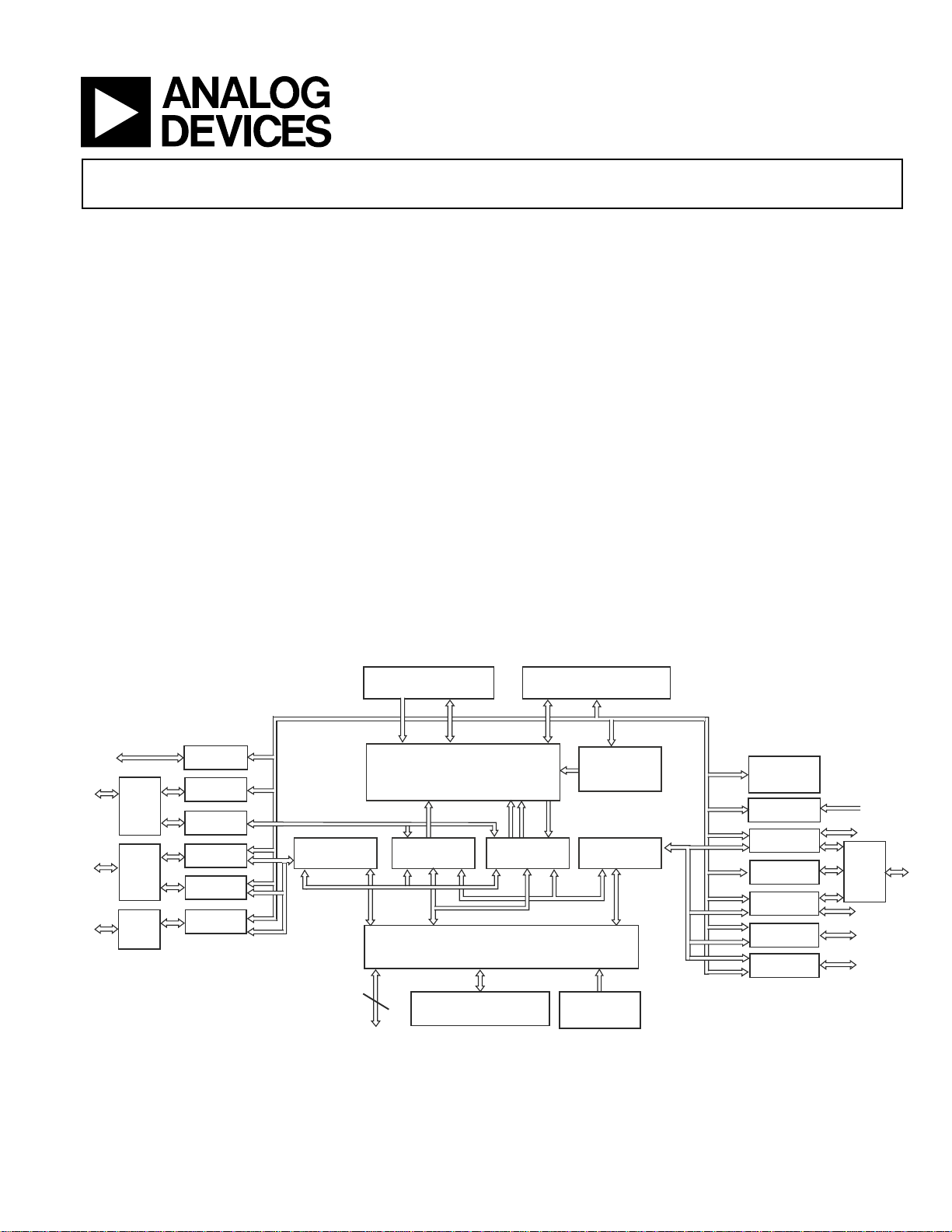
Figure 1. Functional Block Diagram
One Technology Way, P.O. Box 9106, Norwood, MA 02062-9106 U.S.A.
Tel: 781.329.4700 www.analog.com
Fax: 781.461.3113 ©2011 Analog Devices, Inc. All rights reserved.

ADSP-BF539/ADSP-BF539F
TABLE OF CONTENTS
Features ................................................................. 1
Memory ................................................................ 1
Peripherals ............................................................. 1
Revision History ...................................................... 2
General Description ................................................. 3
Low Power Architecture ......................................... 3
System Integration ................................................ 3
ADSP-BF539/ADSP-BF539F Processor Peripherals ....... 3
Blackfin Processor Core .......................................... 4
Memory Architecture ............................................ 5
DMA Controllers .................................................. 8
Real-Time Clock ................................................... 9
Watchdog Timer .................................................. 9
Timers ............................................................... 9
Serial Ports (SPORTs) .......................................... 10
Serial Peripheral Interface (SPI) Ports ...................... 10
2-Wire Interface ................................................. 10
UART Ports ...................................................... 10
Programmable I/O Pins ........................................ 11
Parallel Peripheral Interface ................................... 12
Controller Area Network (CAN) Interface ................ 12
Media Transceiver MAC layer (MXVR) ................... 13
Dynamic Power Management ................................ 13
Voltage Regulation .............................................. 15
Clock Signals ..................................................... 15
Booting Modes ................................................... 16
Instruction Set Description .................................... 17
Development Tools .............................................. 17
Designing an Emulator Compatible Processor Board ... 18
Example Connections and Layout Considerations ....... 18
MXVR Board Layout Guidelines ............................. 18
Voltage Regulator Layout Guidelines ....................... 19
Related Documents .............................................. 20
Related Signal Chains ........................................... 20
Pin Descriptions .................................................... 21
Specifications ........................................................ 26
Operating Conditions ........................................... 26
Electrical Characteristics ....................................... 27
Absolute Maximum Ratings ................................... 30
ESD Sensitivity ................................................... 30
Package Information ............................................ 30
Timing Specifications ........................................... 31
Output Drive Currents ......................................... 50
Test Conditions .................................................. 52
Thermal Characteristics ........................................ 55
316-Ball CSP_BGA Ball Assignment .. ......................... 56
Outline Dimensions ................................................ 59
Surface-Mount Design .......................................... 59
Automotive Products .............................................. 60
Ordering Guide ..................................................... 60
REVISION HISTORY
1/11—Rev. D to Rev. E
Revised package drawing by specifying package height maxi-
mum in Outline Dimensions .................................... 59
Rev. E | Page 2 of 60 | January 2011

GENERAL DESCRIPTION
ADSP-BF539/ADSP-BF539F
The ADSP-BF539/ADSP-BF539F processors are members of
the Blackfin
Devices, Inc./Intel Micro Signal Architecture (MSA). Blackfin
processors combine a dual-MAC, state-of-the-art signal processing engine, the advantages of a clean, orthogonal RISC-like
microprocessor instruction set, and single-instruction, multiple-data (SIMD) multimedia capabilities into a single
instruction set architecture.
The ADSP-BF539/ADSP-BF539F processors are completely
code compatible with other Blackfin processors, differing only
with respect to performance, peripherals, and on-chip memory.
These features are shown in Table 1.
By integrating a rich set of industry-leading system peripherals
and memory, Blackfin processors are the platform of choice for
next generation applications that require RISC-like programmability, multimedia support, and leading edge signal
processing in one integrated package.
Table 1. Processor Features
Feature ADSP-BF539 ADSP-BF539F8
SPORTs 4 4
UARTs 3 3
SPI 3 3
TWI 2 2
CAN 1 1
MXVR 1 1
PPI 1 1
Internal 8M bit
Parallel Flash
Instruction
SRAM/Cache
Instruction SRAM 64K bytes 64K bytes
Data SRAM/Cache 32K bytes 32K bytes
Data SRAM 32K bytes 32K bytes
Scratchpad 4K bytes 4K bytes
Maximum
Frequency
Package Option BC-316 BC-316
®
family of products, incorporating the Analog
—1
16K bytes 16K bytes
533 MHz
1066 MMACS
533 MHz
1066 MMACS
LOW POWER ARCHITECTURE
Blackfin processors provide world class power management and
performance. Blackfin processors are designed in a low power
and low voltage design methodology and feature dynamic
power management, the ability to vary both the voltage and frequency of operation to significantly lower overall power
consumption. Varying the voltage and frequency can result in a
substantial reduction in power consumption, compared with
simply varying the frequency of operation. This translates into
longer battery life and lower heat dissipation.
SYSTEM INTEGRATION
The ADSP-BF539/ADSP-BF539F processors are highly integrated system-on-a-chip solutions for the next generation of
industrial and automotive applications including audio and
video signal processing. By combining advanced memory configurations, such as on-chip flash memory, with industrystandard interfaces with a high performance signal processing
core, users can develop cost-effective solutions quickly without
the need for costly external components. The system peripherals
include a MOST Network Media Transceiver (MXVR), three
UART ports, three SPI ports, four serial ports (SPORT), one
CAN interface, two 2-wire interfaces (TWI), four general-purpose timers (three with PWM capability), a real-time clock, a
watchdog timer, a parallel peripheral interface, general-purpose
I/O, and general-purpose flag pins.
ADSP-BF539/ADSP-BF539F PROCESSOR PERIPHERALS
The ADSP-BF539/ADSP-BF539F processors contain a rich set
of peripherals connected to the core via several high bandwidth
buses, providing flexibility in system configuration as well as
excellent overall system performance (see Figure 1 on Page 1).
The general-purpose peripherals include functions such as
UART, timers with PWM (pulse-width modulation) and pulse
measurement capability, general-purpose flag I/O pins, a realtime clock, and a watchdog timer. This set of functions satisfies
a wide variety of typical system support needs and is augmented
by the system expansion capabilities of the device. In addition to
these general-purpose peripherals, the processors contain high
speed serial and parallel ports for interfacing to a variety of
audio, video, and modem codec functions. An MXVR transceiver transmits and receives audio and video data and control
information on a MOST automotive multimedia network. A
CAN 2.0B controller is provided for automotive control networks. An interrupt controller manages interrupts from the onchip peripherals or external sources. And power management
control functions tailor the performance and power characteristics of the processor and system to many application scenarios.
All of the peripherals, GPIO, CAN, TWI, real-time clock, and
timers, are supported by a flexible DMA structure. There are
also four separate memory DMA channels dedicated to data
transfers between the processor’s various memory spaces,
including external SDRAM and asynchronous memory. Multiple on-chip buses running at up to 133 MHz provide enough
bandwidth to keep the processor core running along with activity on all of the on-chip and external peripherals.
The ADSP-BF539/ADSP-BF539F processors include an on-chip
voltage regulator in support of the processor’s dynamic power
management capability. The voltage regulator provides a range
of core voltage levels from V
bypassed at the user's discretion.
. The voltage regulator can be
DDEXT
Rev. E | Page 3 of 60 | January 2011
ADSP-BF539/ADSP-BF539F
SEQUENCER
ALIGN
DECODE
LOOP BUFFER
16
16
8888
40 40
A0 A1
BARREL
SHIFTER
DATA ARITHMETIC UNIT
CONTROL
UNIT
R7.H
R6.H
R5.H
R4.H
R3.H
R2.H
R1.H
R0.H
R7.L
R6.L
R5.L
R4.L
R3.L
R2.L
R1.L
R0.L
AS TAT
40 40
32
32
32
32
32
32
32LD0
LD1
SD
DAG0
DAG1
ADDRESS ARITHMETIC UNIT
I3
I2
I1
I0
L3
L2
L1
L0
B3
B2
B1
B0
M3
M2
M1
M0
SP
FP
P5
P4
P3
P2
P1
P0
DA1
DA0
32
32
32
PREG
RAB
32
TO MEMORY
BLACKFIN PROCESSOR CORE
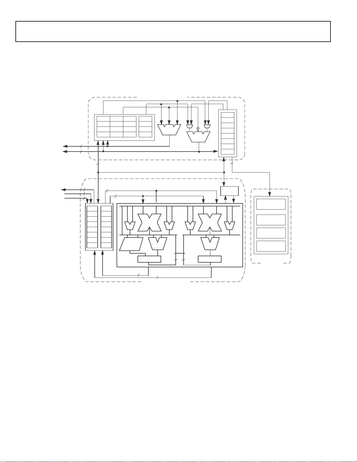
As shown in Figure 2, the Blackfin processor core contains two
16-bit multipliers, two 40-bit accumulators, two 40-bit ALUs,
four video ALUs, and a 40-bit shifter. The computation units
process 8-bit, 16-bit, or 32-bit data from the register file.
The compute register file contains eight 32-bit registers. When
performing compute operations on 16-bit operand data, the
register file operates as 16 independent 16-bit registers. All
operands for compute operations come from the multiported
register file and instruction constant fields.
Each MAC can perform a 16-bit by 16-bit multiply in each
cycle, accumulating the results into the 40-bit accumulators.
Signed and unsigned formats, rounding, and saturation are
supported.
The ALUs perform a traditional set of arithmetic and logical
operations on 16-bit or 32-bit data. In addition, many special
instructions are included to accelerate various signal processing
tasks. These include bit operations such as field extract and population count, modulo 2
and rounding, and sign/exponent detection. The set of video
instructions include byte alignment and packing operations, 16bit and 8-bit adds with clipping, 8-bit average operations, and 8bit subtract/absolute value/accumulate (SAA) operations. Also
provided are the compare/select and vector search instructions.
For certain instructions, two 16-bit ALU operations can be performed simultaneously on register pairs (a 16-bit high half and
16-bit low half of a compute register). By also using the second
ALU, quad 16-bit operations are possible.
32
multiply, divide primitives, saturation
Figure 2. Blackfin Processor Core
The 40-bit shifter can perform shifts and rotates and is used to
support normalization, field extract, and field deposit
instructions.
The program sequencer controls the flow of instruction execution, including instruction alignment and decoding. For
program flow control, the sequencer supports PC relative and
indirect conditional jumps (with static branch prediction), and
subroutine calls. Hardware is provided to support zero overhead looping. The architecture is fully interlocked, meaning that
the programmer need not manage the pipeline when executing
instructions with data dependencies.
The address arithmetic unit provides two addresses for simultaneous dual fetches from memory. It contains a multiported
register file consisting of four sets of 32-bit index, modify,
length, and base registers (for circular buffering), and eight
additional 32-bit pointer registers (for C-style indexed stack
manipulation).
Rev. E | Page 4 of 60 | January 2011
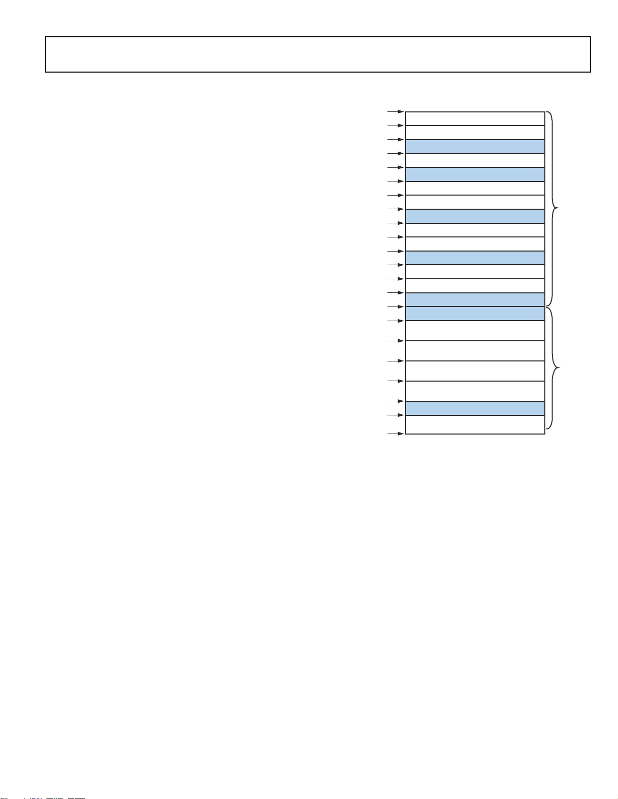
Blackfin processors support a modified Harvard architecture in
RESERVED
CORE MMR REGISTERS (2M BYTES)
RESERVED
SCRATCHPAD SRAM (4K BYTES)
INSTRUCTION SRAM (64K BYTES)
SYSTEM MMR REGISTERS (2M BYTES)
RESERVED
RESERVED
DATA BANK B SRAM / CACHE (16K BYTES)
DATA BANK B SRAM (16K BYTES)
DATA BANK A SRAM / CACHE (16K BYTES)
ASYNC MEMORY BANK 3 (1M BYTES) OR
ON-CHIP FLASH (ADSP-BF539F ONLY)
ASYNC MEMORY BANK 2 (1M BYTES) OR
ON-CHIP FLASH (ADSP-BF539F ONLY)
ASYNC MEMORY BANK 1 (1M BYTES) OR
ON-CHIP FLASH (ADSP-BF539F ONLY)
ASYNC MEMORY BANK 0 (1M
BYTES) OR
ON-CHIP FLASH (ADSP-BF539F ONLY)
SDRAM MEMORY
(16M BYTES TO 128M BYTES)
INSTRUCTION SRAM / CACHE (16K BYTES)
IN
T
E
RN
A
L
M
E
M
O
R
Y
M
A
P
E
XT
E
R
N
A
L
M
EM
OR
Y
M
A
P
0xFFFF FFFF
0xFFE0 0000
0xFFB0 0000
0xFFA1 4000
0xFFA1 0000
0xFF90 8000
0xFF90 4000
0xFF80 8000
0xFF80 4000
0xEF00 0000
0x2040 0000
0x2030 0000
0x2020 0000
0x2010 0000
0x2000 0000
0x0800 0000
0x0000 0000
0xFFC0 0000
0xFFB0 1000
0xFFA0 0000
RESERVED
RESERVED
DATA BANK A SRAM (16K BYTES)
0xFF90 0000
0xFF80 0000
RESERVED
combination with a hierarchical memory structure. Level 1 (L1)
memories are those that typically operate at the full processor
speed with little or no latency. At the L1 level, the instruction
memory holds instructions only. The two data memories hold
data, and a dedicated scratchpad data memory stores stack and
local variable information.
In addition, multiple L1 memory blocks are provided, offering a
configurable mix of SRAM and cache. The memory management Unit (MMU) provides memory protection for individual
tasks that can be operating on the core and can protect system
registers from unintended access.
The architecture provides three modes of operation: user mode,
supervisor mode, and emulation mode. User mode has
restricted access to certain system resources, thus providing a
protected software environment, while supervisor mode has
unrestricted access to the system and core resources.
The Blackfin processor instruction set has been optimized so
that 16-bit opcodes represent the most frequently used instructions, resulting in excellent compiled code density. Complex
DSP instructions are encoded into 32-bit opcodes, representing
fully featured multifunction instructions. Blackfin processors
support a limited multi-issue capability, where a 32-bit instruction can be issued in parallel with two 16-bit instructions,
allowing the programmer to use many of the core resources in a
single instruction cycle.
The Blackfin processor assembly language uses an algebraic syntax for ease of coding and readability. The architecture has been
optimized for use in conjunction with the C/C++ compiler,
resulting in fast and efficient software implementations.
ADSP-BF539/ADSP-BF539F
MEMORY ARCHITECTURE
The ADSP-BF539/ADSP-BF539F processors view memory as a
single unified 4G byte address space, using 32-bit addresses. All
resources, including internal memory, external memory, and
I/O control registers, occupy separate sections of this common
address space. The memory portions of this address space are
arranged in a hierarchical structure to provide a good cost/performance balance of some very fast, low latency on-chip
memory as cache or SRAM, and larger, lower cost and performance off-chip memory systems. See Figure 3.
The L1 memory system is the primary highest performance
memory available to the Blackfin processor. The off-chip memory system, accessed through the external bus interface unit
(EBIU), provides expansion with SDRAM, flash memory, and
SRAM, optionally accessing up to 132M bytes of physical
memory.
The memory DMA controller provides high bandwidth data
movement capability. It performs block transfers of code or data
between the internal memory and the external memory spaces.
Internal (On-Chip) Memory
The ADSP-BF539/ADSP-BF539F processor has three blocks of
on-chip memory, providing high bandwidth access to the core.
Rev. E | Page 5 of 60 | January 2011
Figure 3. ADSP-BF539/ADSP-BF539F Internal/External Memory Map
The first is the L1 instruction memory, consisting of 80K bytes
SRAM, of which 16K bytes can be configured as a four-way setassociative cache. This memory is accessed at full processor
speed.
The second on-chip memory block is the L1 data memory, consisting of two banks of up to 32K bytes each. Each memory bank
is configurable, offering both cache and SRAM functionality.
This memory block is accessed at full processor speed.
The third memory block is a 4K byte scratch pad SRAM, which
runs at the same speed as the L1 memories, but is only accessible
as data SRAM and cannot be configured as cache memory.
External (Off-Chip) Memory
External memory is accessed via the EBIU. This 16-bit interface
provides a glueless connection to a bank of synchronous DRAM
(SDRAM) as well as up to four banks of asynchronous memory
devices including flash, EPROM, ROM, SRAM, and memory
mapped I/O devices.
ADSP-BF539/ADSP-BF539F
VSS
FRESET
FCE
RESET
DATA15-0
GND
VDDEXT
ADDR19
-
ARE
AWE
GND
DATA15
-
0
ARDY
AWE
VCC
BYTE
RESET
CE
AMS3
-
0
RESET
ARE
ARDY
ADDR19
-
1
OE
WE
RY/BY
V
DDEXT
ADSP-BF539F
PACKAGE
B
S29AL008J
FLASH DIE
AMS3
-
0
DQ15-0
A18
-
0
WP
NC
The PC133-compliant SDRAM controller can be programmed
to interface to up to 128M bytes of SDRAM. The SDRAM controller allows one row to be open for each internal SDRAM
bank, for up to four internal SDRAM banks, improving overall
system performance.
The asynchronous memory controller can be programmed to
control up to four banks of devices with very flexible timing
parameters for a wide variety of devices. Each bank occupies a
1M byte segment regardless of the size of the devices used, so
that these banks will only be contiguous if each is fully populated with 1M byte of memory.
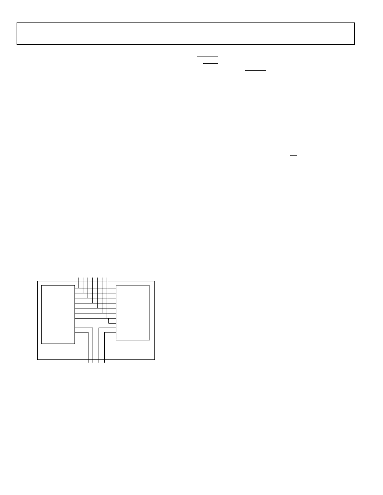
Flash Memory (ADSP-BF539F Only)
The ADSP-BF539F8 processor contains a separate flash die,
connected to the EBIU bus, within the package of the processor.
Figure 4 shows how the flash memory die and Blackfin proces-
sor die are connected.
The ADSP-BF539F8 contains an 8M bit (512K × 16-bit) bottom
boot sector Spansion S29AL008J known good die flash memory.
Additional information for this product can be found in the
Spansion data sheet at www.spansion.com. Features include the
following:
• Access times as fast as 70 ns (EBIU registers must be set
appropriately)
• Sector protection
• One million write cycles per sector
• 20 year data retention
The flash chip enable pin FCE
AMS3–1
to AMS0
through a printed circuit board trace. When connected
, the Blackfin processor can boot from the flash die.
When connected to AMS3–1
must be connected to AMS0 or
, the flash memory appears as nonvolatile memory in the processor memory map, shown in
Figure 3.
Flash Memory Programming
The ADSP-BF539F8 flash memory can be programmed before
or after mounting on the printed circuit board.
To program the flash prior to mounting on the printed circuit
board, use a hardware programming tool that can provide the
data, address, and control stimuli to the flash die through the
external pins on the package. During this programming, V
DDEXT
and GND must be provided to the package and the Blackfin
must be held in reset with bus request (BR
) asserted and a
CLKIN provided.
The VisualDSP++ tools can be used to program the flash memory after the device is mounted on a printed circuit board.
Flash Memory Sector Protection
To use the sector protection feature, a high voltage (+8.5 V to
+12.5 V) must be applied to the flash FRESET
pin. Refer to the
flash data sheet for details.
I/O Memory Space
Blackfin processors do not define a separate I/O space. All
resources are mapped through the flat 32-bit address space. Onchip I/O devices have their control registers mapped into memory mapped registers (MMRs) at addresses near the top of the
4G byte address space. These are separated into two smaller
blocks, one of which contains the control MMRs for all core
functions, and the other of which contains the registers needed
for setup and control of the on-chip peripherals outside of the
core. The MMRs are accessible only in supervisor mode and
appear as reserved space to on-chip peripherals.
Figure 4. Internal Connection of Flash Memory (ADSP-BF539F8)
The Blackfin processor connects to the flash memory die with
address, data, chip enable, write enable, and output enable controls as if it were an external memory device. Note that the
write-protect input pin to the flash is not connected and inaccessible, disabling this feature.
Booting
The ADSP-BF539/ADSP-BF539F processors contain a small
boot kernel, which configures the appropriate peripheral for
booting. If the processors are configured to boot from boot
ROM memory space, they start executing from the on-chip boot
ROM. For more information, see Booting Modes on Page 16.
Event Handling
The event controller handles all asynchronous and synchronous
events to the processor. The processors provide event handling
that supports both nesting and prioritization. Nesting allows
multiple event service routines to be active simultaneously. Prioritization ensures that servicing of a higher priority event takes
precedence over servicing of a lower priority event. The controller provides support for five different types of events:
• Emulation – An emulation event causes the processor to
enter emulation mode, allowing command and control of
the processor via the JTAG interface.
• Reset – This event resets the processor.
Rev. E | Page 6 of 60 | January 2011

ADSP-BF539/ADSP-BF539F
• Nonmaskable Interrupt (NMI) – The NMI event can be
generated by the software watchdog timer or by the NMI
input signal to the processor. The NMI event is frequently
used as a power-down indicator to initiate an orderly shutdown of the system.
• Exceptions – Events that occur synchronously to program
flow (i.e., the exception will be taken before the instruction
is allowed to complete). Conditions such as data alignment
violations and undefined instructions cause exceptions.
• Interrupts – Events that occur asynchronously to program
flow. They are caused by input pins, timers, and other
peripherals, as well as by an explicit software instruction.
Each event type has an associated register to hold the return
address and an associated return-from-event instruction. When
an event is triggered, the state of the processor is saved on the
supervisor stack.
The ADSP-BF539/ADSP-BF539F processor’s event controller
consists of two stages, the core event controller (CEC) and the
system interrupt controller (SIC). The core event controller
works with the system interrupt controller to prioritize and control all system events. Conceptually, interrupts from the
peripherals enter into the SIC and are then routed directly into
the general-purpose interrupts of the CEC.
Core Event Controller (CEC)
The CEC supports nine general-purpose interrupts (IVG15– 7),
in addition to the dedicated interrupt and exception events. Of
these general-purpose interrupts, the two lowest priority interrupts (IVG15–14) are recommended to be reserved for software
interrupt handlers, leaving seven prioritized interrupt inputs to
support the processor’s peripherals. Table 2 describes the inputs
to the CEC, identifies their names in the event vector table
(EVT), and lists their priorities.
System Interrupt Controller (SIC)
The system interrupt controller (SIC) provides the mapping and
routing of events from the many peripheral interrupt sources to
the prioritized general-purpose interrupt inputs of the CEC.
Although the ADSP-BF539/ADSP-BF539F processors provide a
default mapping, the user can alter the mappings and priorities
of interrupt events by writing the appropriate values into the
interrupt assignment registers (SIC_IARx). Table 3 describes
the inputs into the SIC and the default mappings into the CEC.
Event Control
The ADSP-BF539/ADSP-BF539F processors provide the user
with a very flexible mechanism to control the processing of
events. In the CEC, three registers are used to coordinate and
control events. Each register is 32 bits wide:
• CEC interrupt latch register (ILAT) – The ILAT register
indicates when events have been latched. The appropriate
bit is set when the processor has latched the event and is
cleared when the event has been accepted into the system.
This register is updated automatically by the controller, but
it can also be written to clear (cancel) latched events. This
register may be read while in supervisor mode and may
only be written while in supervisor mode when the corresponding IMASK bit is cleared.
• CEC interrupt mask register (IMASK) – The IMASK register controls the masking and unmasking of individual
events. When a bit is set in the IMASK register, that event is
unmasked and will be processed by the CEC when asserted.
A cleared bit in the IMASK register masks the event,
preventing the processor from servicing the event even
though the event can be latched in the ILAT register. This
register can be read or written while in supervisor mode.
General-purpose interrupts can be globally enabled and
disabled with the STI and CLI instructions, respectively.
• CEC interrupt pending register (IPEND) – The IPEND
register keeps track of all nested events. A set bit in the
IPEND register indicates whether the event is currently
active or nested at some level. This register is updated automatically by the controller but can be read while in
supervisor mode.
The SIC allows further control of event processing by providing
three 32-bit interrupt control and status registers. Each register
contains a bit corresponding to each of the peripheral interrupt
events shown in Table 3 on Page 8.
• SIC interrupt mask registers (SIC_IMASKx) – These registers control the masking and unmasking of each peripheral
interrupt event. When a bit is set in these registers, that
peripheral event is unmasked and will be processed by the
system when asserted. A cleared bit in these registers masks
the peripheral event, preventing the processor from servicing the event.
• SIC interrupt status registers (SIC_ISRx) – As multiple
peripherals can be mapped to a single event, these registers
allow the software to determine which peripheral event
source triggered the interrupt. A set bit indicates that the
peripheral is asserting the interrupt, and a cleared bit indicates that the peripheral is not asserting the event.
• SIC interrupt wake-up enable registers (SIC_IWRx) – By
enabling the corresponding bit in these registers, a peripheral can be configured to wake up the processor, should the
core be idled or in sleep mode when the event is generated.
(For more information, see Dynamic Power Management
on Page 13.)
Because multiple interrupt sources can map to a single generalpurpose interrupt, multiple pulse assertions can occur simultaneously, before or during interrupt processing for an interrupt
event already detected on this interrupt input. The IPEND register contents are monitored by the SIC as the interrupt
acknowledgement.
The appropriate ILAT register bit is set when an interrupt rising
edge is detected (detection requires two core clock cycles). The
bit is cleared when the respective IPEND register bit is set. The
IPEND bit indicates that the event has entered into the processor pipeline. At this point the CEC will recognize and queue the
next rising edge event on the corresponding event input. The
minimum latency from the rising edge transition of the
Rev. E | Page 7 of 60 | January 2011

ADSP-BF539/ADSP-BF539F
general-purpose interrupt to the IPEND output asserted is three
core clock cycles; however, the latency can be much higher,
depending on the activity within and the state of the processor.
Table 2. Core Event Controller (CEC)
Priority
(0 is Highest)
0Emulation/Test ControlEMU
1 Reset RST
2 Nonmaskable Interrupt NMI
3Exception EVX
4 Reserved —
5 Hardware Error IVHW
6 Core Timer IVTMR
7 General Interrupt 7 IVG7
8 General Interrupt 8 IVG8
9 General Interrupt 9 IVG9
10 General Interrupt 10 IVG10
11 General Interrupt 11 IVG11
12 General Interrupt 12 IVG12
13 General Interrupt 13 IVG13
14 General Interrupt 14 IVG14
15 General Interrupt 15 IVG15
Event Class EVT Entry
Table 3. System and Core Event Mapping
Core
Event Source
PLL Wake-Up Interrupt IVG7
DMA Controller 0 Error IVG7
DMA Controller 1 Error IVG7
PPI Error Interrupt IVG7
SPORT0 Error Interrupt IVG7
SPORT1 Error Interrupt IVG7
SPORT2 Error Interrupt IVG7
SPORT3 Error Interrupt IVG7
MXVR Synchronous Data Interrupt IVG7
SPI0 Error Interrupt IVG7
SPI1 Error Interrupt IVG7
SPI2 Error Interrupt IVG7
UART0 Error Interrupt IVG7
UART1 Error Interrupt IVG7
UART2 Error Interrupt IVG7
CAN Error Interrupt IVG7
Real-Time Clock Interrupt IVG8
DMA0 Interrupt (PPI) IVG8
DMA1 Interrupt (SPORT0 Rx) IVG9
DMA2 Interrupt (SPORT0 Tx) IVG9
Event Name
Table 3. System and Core Event Mapping (Continued)
Core
Event Source
DMA3 Interrupt (SPORT1 Rx) IVG9
DMA4 Interrupt (SPORT1 Tx) IVG9
DMA8 Interrupt (SPORT2 Rx) IVG9
DMA9 Interrupt (SPORT2 Tx) IVG9
DMA10 Interrupt (SPORT3 Rx) IVG9
DMA11 Interrupt (SPORT3 Tx) IVG9
DMA5 Interrupt (SPI0) IVG10
DMA14 Interrupt (SPI1) IVG10
DMA15 Interrupt (SPI2) IVG10
DMA6 Interrupt (UART0 Rx) IVG10
DMA7 Interrupt (UART0 Tx) IVG10
DMA16 Interrupt (UART1 Rx) IVG10
DMA17 Interrupt (UART1 Tx) IVG10
DMA18 Interrupt (UART2 Rx) IVG10
DMA19 Interrupt (UART2 Tx) IVG10
Timer0, Timer1, Timer2 Interrupts IVG11
TWI0 Interrupt IVG11
TWI1 Interrupt IVG11
CAN Receive Interrupt IVG11
CAN Transmit Interrupt IVG11
MXVR Status Interrupt IVG11
MXVR Control Message Interrupt IVG11
MXVR Asynchronous Packet Interrupt IVG11
Programmable Flags Interrupts IVG12
MDMA0 Stream 0 Interrupt IVG13
MDMA0 Stream 1 Interrupt IVG13
MDMA1 Stream 0 Interrupt IVG13
MDMA1 Stream 1 Interrupt IVG13
Software Watchdog Timer IVG13
Event Name
DMA CONTROLLERS
The processors have multiple, independent DMA controllers
that support automated data transfers with minimal overhead
for the processor core. DMA transfers can occur between the
ADSP-BF539/ADSP-BF539F processor internal memories and
any of its DMA capable peripherals. Additionally, DMA transfers can be accomplished between any of the DMA-capable
peripherals and external devices connected to the external
memory interfaces, including the SDRAM controller and the
asynchronous memory controller. DMA capable peripherals
include the SPORTs, SPI ports, UARTs, and PPI. Each individual DMA capable peripheral has at least one dedicated DMA
channel. In addition, the MXVR peripheral has its own dedicated DMA controller, which supports its own unique set of
operating modes.
Rev. E | Page 8 of 60 | January 2011
ADSP-BF539/ADSP-BF539F
RTXO
C1 C2
X1
SUGGESTED COMPONENTS:
ECLIPTEK EC38J (THROUGH-HOLE PACKAGE)
EPSON MC405 12 pF LOAD (SURFACE-MOUNT PACKAGE)
C1 = 22pF
C2 = 22pF
R1 = 10M:
NOTE: C1 AND C2 ARE SPECIFIC TO CRYSTAL SPECIFIED FOR X1.
CONTACT CRYSTAL MANUFACTURER FOR DETAILS. C1 AND C2
SPECIFICATIONS ASSUME BOARD TRACE CAPACITANCE OF 3pF.
RTXI
R1
The DMA controllers support both 1-dimensional (1-D) and 2dimensional (2-D) DMA transfers. DMA transfer initialization
can be implemented from registers or from sets of parameters
called descriptor blocks.
The 2-D DMA capability supports arbitrary row and column
sizes up to 64K elements by 64K elements and arbitrary row and
column step sizes up to ±32K elements. Furthermore, the column step size can be less than the row step size, allowing
implementation of interleaved data streams. This feature is
especially useful in video applications where data can be
deinterleaved on the fly.
Examples of DMA types supported by the processor’s DMA
controller include:
• A single, linear buffer that stops upon completion
• A circular, auto-refreshing buffer that interrupts on each
full or fractionally full buffer
• 1-D or 2-D DMA using a linked list of descriptors
•2-D DMA using an array of descriptors, specifying only the
base DMA address within a common page
In addition to the dedicated peripheral DMA channels, there are
four memory DMA channels provided for transfers between the
various memories of the ADSP-BF539/ADSP-BF539F processor
system. This enables transfers of blocks of data between any of
the memories—including external SDRAM, ROM, SRAM, and
flash memory—with minimal processor intervention. Memory
DMA transfers can be controlled by a very flexible descriptorbased methodology or by a standard register-based autobuffer
mechanism.
REAL-TIME CLOCK
The ADSP-BF539/ADSP-BF539F processor real-time clock
(RTC) provides a robust set of digital watch features, including
current time, stopwatch, and alarm. The RTC is clocked by a
32.768 kHz crystal external to the Blackfin processors. The RTC
peripheral has dedicated power supply pins so that it can remain
powered up and clocked even when the rest of the processor is
in a low power state. The RTC provides several programmable
interrupt options, including interrupt per second, minute, hour,
or day clock ticks, interrupt on programmable stopwatch countdown, or interrupt at a programmed alarm time.
The 32.768 kHz input clock frequency is divided down to a 1 Hz
signal by a prescaler. The counter function of the timer consists
of four counters: a 60-second counter, a 60-minute counter, a
24-hour counter, and an 32,768-day counter.
When enabled, the alarm function generates an interrupt when
the output of the timer matches the programmed value in the
alarm control register. There are two alarms: the first alarm is
for a time of day. The second alarm is for a day and time of
that day.
The stopwatch function counts down from a programmed
value, with one second resolution. When the stopwatch is
enabled and the counter underflows, an interrupt is generated.
Like the other peripherals, the RTC can wake up the processor
from sleep mode upon generation of any RTC wake-up event.
Additionally, an RTC wake-up event can wake up the processor
from deep sleep mode, and wake up the on-chip internal voltage
regulator from a powered down state.
Connect RTC pins RTXI and RTXO with external components
as shown in Figure 5.
Figure 5. External Components for RTC
WATCHDOG TIMER
The processors include a 32-bit timer that can be used to implement a software watchdog function. A software watchdog can
improve system availability by forcing the processor to a known
state through generation of a hardware reset, nonmaskable
interrupt (NMI), or general-purpose interrupt, if the timer
expires before being reset by software. Programs initialize the
count value of the timer, enable the appropriate interrupt, and
then enable the timer. Thereafter, the software must reload the
counter before it counts to zero from the programmed value.
This protects the system from remaining in an unknown state
where software, which would normally reset the timer, has
stopped running due to an external noise condition or software
error.
If configured to generate a hardware reset, the watchdog timer
resets both the core and the processor peripherals. After a reset,
software can determine if the watchdog was the source of the
hardware reset by interrogating a status bit in the watchdog
timer control register.
The timer is clocked by the system clock (SCLK), at a maximum
frequency of f
SCLK
.
TIMERS
There are four general-purpose programmable timer units in
the ADSP-BF539/ADSP-BF539F processors. Three timers have
an external pin that can be configured either as a pulse-width
modulator (PWM) or timer output, as an input to clock the
timer, or as a mechanism for measuring pulse widths and
periods of external events. These timers can be synchronized to
Rev. E | Page 9 of 60 | January 2011

ADSP-BF539/ADSP-BF539F
SPI Clock Rate
f
SCLK
2SPIx_BAUD×
------------------------------------
=
an external clock input to the PF1 pin (TACLK), an external
clock input to the PPI_CLK pin (TMRCLK), or to the internal
SCLK.
The timer units can be used in conjunction with UART0 to
measure the width of the pulses in the data stream to provide an
auto-baud detect function for a serial channel.
The timers can generate interrupts to the processor core providing periodic events for synchronization, either to the system
clock or to a count of external signals.
In addition to the three general-purpose programmable timers,
a fourth timer is also provided. This extra timer is clocked by the
internal processor clock and is typically used as a system tick
clock for generation of operating system periodic interrupts.
SERIAL PORTS (SPORTS)
The ADSP-BF539/ADSP-BF539F processors incorporate four
dual-channel synchronous serial ports for serial and multiprocessor communications. The SPORTs support the following
features:
2
•I
S capable operation.
• Bidirectional operation – Each SPORT has two sets of independent transmit and receive pins, enabling 16 channels of
2
I
S stereo audio.
• Buffered (8-deep) transmit and receive ports – Each port
has a data register for transferring data words to and from
other processor components and shift registers for shifting
data in and out of the data registers.
• Clocking – Each transmit and receive port can either use an
external serial clock or generate its own, in frequencies
ranging from (f
• Word length – Each SPORT supports serial data words
from 3 bits to 32 bits in length, transferred most significant
bit first or least significant bit first.
• Framing – Each transmit and receive port can run with or
without frame sync signals for each data word. Frame sync
signals can be generated internally or externally, active high
or low, and with either of two pulse widths and early or late
frame sync.
• Companding in hardware – Each SPORT can perform
A-law or μ-law companding according to ITU recommendation G.711. Companding can be selected on the transmit
and/or receive channel of the SPORT without additional
latencies.
• DMA operatio ns with single-cycle overhead – Each SPORT
can automatically receive and transmit multiple buffers of
memory data. The processor can link or chain sequences of
DMA transfers between a SPORT and memory.
• Interrupts – Each transmit and receive port generates an
interrupt upon completing the transfer of a data word or
after transferring an entire data buffer or buffers through
DMA.
• Multichannel capability – Each SPORT supports 128 channels out of a 1024-channel window and is compatible with
the H.100, H.110, MVIP-90, and HMVIP standards.
/131,070) Hz to (f
SCLK
SCLK
/2) Hz.
SERIAL PERIPHERAL INTERFACE (SPI) PORTS
The processors incorporate three SPI-compatible ports that
enable the processor to communicate with multiple SPI compatible devices.
The SPI interface uses three pins for transferring data: two data
pins (master output-slave input, MOSIx, and master input-slave
output, MISOx) and a clock pin (serial clock, SCKx). An SPI
chip select input pin (SPIxSS
) lets other SPI devices select the
processor. For SPI0, seven SPI chip select output pins
(SPI0SEL7–1
) let the processor select other SPI devices. SPI1
and SPI2 each have a single SPI chip select output pin
(SPI1SEL1
and SPI2SEL1) for SPI point-to-point communication. Each of the SPI select pins is a reconfigured GPIO pin.
Using these pins, the SPI ports provide a full-duplex, synchronous serial interface, which supports both master/slave modes
and multimaster environments.
The SPI ports’ baud rate and clock phase/polarities are programmable, and they each have an integrated DMA controller,
configurable to support transmit or receive data streams. Each
SPI DMA controller can only service unidirectional accesses at
any given time.
The SPI port clock rate is calculated as:
where the 16-bit SPIx_BAUD register contains a value of 2 to
65,535.
During transfers, the SPI port simultaneously transmits and
receives by serially shifting data in and out on its two serial data
lines. The serial clock line synchronizes the shifting and sampling of data on the two serial data lines.
2-WIRE INTERFACE
The processors incorporate two 2-wire interface (TWI) modules
that are compatible with the Philips Inter-IC bus standard. The
TWI modules offer the capabilities of simultaneous master and
slave operation, support for 7-bit addressing, and multimedia
data arbitration. The TWI also includes master clock synchronization and support for clock low extension.
The TWI interface uses two pins for transferring clock (SCLx)
and data (SDAx) and supports the protocol at speeds up to
400 kbps.
The TWI interface pins are compatible with 5 V logic levels.
UART PORTS
The processors incorporate three full-duplex universal asynchronous receiver/transmitter (UART) ports, which are fully
compatible with PC standard UARTs. The UART ports provide
a simplified UART interface to other peripherals or hosts, supporting full-duplex, DMA supported, asynchronous transfers of
serial data. The UART ports include support for 5 data bits to
8 data bits, 1 stop bit or 2 stop bits, and none, even, or odd parity. The UART ports support two modes of operation:
Rev. E | Page 10 of 60 | January 2011

ADSP-BF539/ADSP-BF539F
UART Clock Rate
f
SCLK
16 UART_Divisor×
--------------------------------------------
=
• PIO (programmed I/O) – The processor sends or receives
data by writing or reading I/O mapped UART registers.
The data is double buffered on both transmit and receive.
• DMA (direct memory access) – The DMA controller transfers both transmit and receive data. This reduces the
number and frequency of interrupts required to transfer
data to and from memory. Each UART has two dedicated
DMA channels, one for transmit and one for receive. These
DMA channels have lower default priority than most DMA
channels because of their relatively low service rates.
Each UART port’s baud rate, serial data format, error code generation and status, and interrupts are programmable:
• Supporting bit rates ranging from (f
/16) bits per second.
(f
SCLK
/1,048,576) to
SCLK
• Supporting data formats from 7 bits to 12 bits per frame.
• Both transmit and receive operations can be configured to
generate maskable interrupts to the processor.
Each UART port’s clock rate is calculated as:
where the 16-bit UART_Divisor comes from the UARTx_DLH
register (most significant 8 bits) and UARTx_DLL register (least
significant 8 bits).
In conjunction with the general-purpose timer functions, autobaud detection is supported on UART0.
The capabilities of the UARTs are further extended with support for the Infrared Data Association (IrDA
®
) Serial Infrared
Physical Layer Link Specification (SIR) protocol.
PROGRAMMABLE I/O PINS
The ADSP-BF539/ADSP-BF539F processor has numerous
peripherals that may not all be required for every application.
Therefore, many of the pins have a secondary function as programmable I/O pins. There are two types of programmable I/O
pins with slightly different functionality: programmable flags
and general-purpose I/O.
Programmable Flags (GPIO Port F)
There are 16 bidirectional, general-purpose programmable flag
(PF15 – 0) pins on GPIO Port F. Each programmable flag can be
individually controlled by manipulation of the flag control, status, and interrupt registers:
• Flag direction control register – Specifies the direction of
each individual PFx pin as input or output.
• Flag control and status registers – The processors employ a
“write one to modify” mechanism that allows any combination of individual flags to be modified in a single
instruction, without affecting the level of any other flags.
Four control registers are provided. One register is written
in order to set flag values, one register is written in order to
clear flag values, one register is written in order to toggle
flag values, and one register is written in order to specify a
flag value. Reading the flag status register allows software to
interrogate the sense of the flags.
• Flag interrupt mask registers – The two flag interrupt mask
registers allow each individual PFx pin to function as an
interrupt to the processor. Similar to the two flag control
registers that are used to set and clear individual flag values,
one flag interrupt mask register sets bits to enable interrupt
function, and the other flag interrupt mask register clears
bits to disable interrupt function. PFx pins defined as
inputs can be configured to generate hardware interrupts,
while output PFx pins can be triggered by software
interrupts.
• Flag interrupt sensitivity registers – The two flag interrupt
sensitivity registers specify whether individual PFx pins are
level- or edge-sensitive and specify—if edge-sensitive—
whether just the rising edge or both the rising and falling
edges of the signal are significant. One register selects the
type of sensitivity, and one register selects which edges are
significant for edge-sensitivity.
The PFx pins can also be used by the SPI0 and PPI ports as
shown in Table 4, depending on how the peripherals are configured. Care must be taken so that these pins are not used for
multiple purposes simultaneously.
General-Purpose I/O Ports C, D, and E
There are 38 general-purpose I/O pins that are multiplexed with
other peripherals. They are arranged into Ports C, D, and E as
shown in Table 4. The GPIO differ from the programmable
flags on Port F in that the GPIO pins cannot generate interrupts
to the processor.
Table 4. Programmable Flag/GPIO Ports
Alternate Programmable Flag/
Peripheral
PPI PF15–3
SPORT2 PE7–0
SPORT3 PE15–8
SPI0 PF7–0
SPI1 PD4–0
SPI2 PD9–5
UART1 PD11–10
UART2 PD13–12
CAN PC1–0
MXVR PC9–4
1
PC1 and PC4 are open-drain when configured as GPIO outputs.
GPIO Port Function
1
1
The general-purpose I/O pins can be individually controlled by
manipulation of the control and status registers. These pins will
not cause interrupts to be generated to the processor but can be
polled to determine their status.
• GPIO direction control register – Specifies the direction of
each individual GPIOx pin as input or output.
• GPIO control and status registers – The processors employ
a “write one to modify” mechanism that allows any combination of individual GPIO pins to be modified in a single
Rev. E | Page 11 of 60 | January 2011

ADSP-BF539/ADSP-BF539F
instruction, without affecting the level of any other GPIO
pin. Four control registers and a data register are provided
for each GPIO port. One register is written in order to set
GPIO pin values, one register is written in order to clear
GPIO pin values, one register is written in order to toggle
GPIO pin values, and one register is written in order to
specify a GPIO input or output. Reading the GPIO data
register allows software to determine the state of the input
GPIO pins.
Note that the GP pin is used to specify the status of the GPIO
pins PC9–PC4 at power up. If GP is tied high, then pins
PC9–PC4 are configured as GPIO after reset. The pins cannot
be reconfigured through software, and special care must be
taken with the MLF pin. If the GP pin is tied low, then the pins
are configured as MXVR pins after reset but can be reconfigured as GPIO pins through software.
PARALLEL PERIPHERAL INTERFACE
The ADSP-BF539/ADSP-BF539F processors provide a parallel
peripheral interface (PPI) that can connect directly to parallel
ADC and DAC converters, video encoders and decoders, and
other general-purpose peripherals. The PPI consists of a dedicated input clock pin, up to 3 frame synchronization pins, and
up to 16 data pins. The input clock supports parallel data rates
up to f
figured as either inputs or outputs.
The PPI supports a variety of general-purpose and ITU-R 656
modes of operation. In general-purpose mode, the PPI provides
half-duplex, bidirectional data transfer with up to 16 bits of
data. Up to 3 frame synchronization signals are also provided.
In ITU-R 656 mode, the PPI provides half-duplex, bidirectional
transfer of 8- or 10-bit video data. Additionally, on-chip decode
of embedded start-of-line (SOL) and start-of-field (SOF) preamble packets are supported.
General-Purpose Mode Descriptions
The general-purpose modes of the PPI are intended to suit a
wide variety of data capture and transmission applications.
Three distinct submodes are supported:
Input Mode
This mode is intended for ADC applications, as well as video
communication with hardware signaling. In its simplest form,
PPI_FS1 is an external frame sync input that controls when to
read data. The PPI_DELAY MMR allows for a delay (in
PPI_CLK cycles) between reception of this frame sync and the
initiation of data reads. The number of input data samples is
user programmable and defined by the contents of the
PPI_COUNT register. The PPI supports 8-bit, and 10-bit
through 16-bit data and are programmable in the
PPI_CONTROL register.
/2 MHz, and the synchronization signals can be con-
SCLK
• Input Mode – Frame syncs and data are inputs into the PPI.
• Frame Capture Mode – Frame syncs are outputs from the
PPI, but data are inputs.
• Output Mode – Frame syncs and data are outputs from
the PPI.
Frame Capture Mode
This mode allows the video source(s) to act as a slave (e.g., for
frame capture). The processors control when to read from the
video source(s). PPI_FS1 is an HSYNC output, and PPI_FS2 is a
VSYNC output.
Output Mode
This mode is used for transmitting video or other data with up
to three output frame syncs. Typically, a single frame sync is
appropriate for data converter applications, whereas two or
three frame syncs could be used for sending video with hardware signaling.
ITU-R 656 Mode Descriptions
The ITU-R 656 modes of the PPI are intended to suit a wide
variety of video capture, processing, and transmission applications. Three distinct submodes are supported:
•Active Video Only Mode
• Vertical Blanking Only Mode
• Entire Field Mode
Active Video Only Mode
This mode is used when only the active video portion of a field
is of interest and not any of the blanking intervals. The PPI will
not read in any data between the end of active video (EAV) and
start of active video (SAV) preamble symbols, or any data present during the vertical blanking intervals. In this mode, the
control byte sequences are not stored to memory; they are
filtered by the PPI. After synchronizing to the start of Field 1,
the PPI ignores incoming samples until it sees an SAV code. The
user specifies the number of active video lines per frame (in the
PPI_COUNT register).
Vertical Blanking Interval Mode
In this mode, the PPI only transfers vertical blanking interval
(VBI) data.
Entire Field Mode
In this mode, the entire incoming bit stream is read in through
the PPI. This includes active video, control preamble sequences,
and ancillary data that can be embedded in horizontal and vertical blanking intervals. Data transfer starts immediately after
synchronization to Field 1.
CONTROLLER AREA NETWORK (CAN) INTERFACE
The ADSP-BF539/ADSP-BF539F processors provide a CAN
controller that is a communication controller implementing the
controller area network (CAN) V2.0B protocol. This protocol is
an asynchronous communications protocol used in both industrial and automotive control systems. CAN is well suited for
control applications due to its ability to communicate reliably
over a network since the protocol incorporates CRC checking,
message error tracking, and fault node confinement.
Rev. E | Page 12 of 60 | January 2011

ADSP-BF539/ADSP-BF539F
The CAN controller is based on a 32-entry mailbox RAM and
supports both the standard and extended identifier (ID) message formats specified in the CAN protocol specification,
Revision 2.0, Part B.
Each mailbox consists of eight 16-bit data words. The data is
divided into fields, which includes a message identifier, a time
stamp, a byte count, up to 8 bytes of data, and several control
bits. Each node monitors the messages being passed on the network. If the identifier in the transmitted message matches an
identifier in one of its mailboxes, then the module knows that
the message was meant for it, passes the data into its appropriate
mailbox, and signals the processor of message arrival with an
interrupt.
The CAN controller can wake up the processor from sleep mode
upon generation of a wake-up event, such that the processor can
be maintained in a low power mode during idle conditions.
Additionally, a CAN wake-up event can wake up the on-chip
internal voltage regulator from the hibernate state.
The electrical characteristics of each network connection are
very stringent; therefore, the CAN interface is typically divided
into two parts: a controller and a transceiver. This allows a single controller to support different drivers and CAN networks.
The ADSP-BF539/ADSP-BF539F CAN module represents the
controller part of the interface. This module’s network I/O is a
single transmit output and a single receive input, which connect
to a line transceiver.
The CAN clock is derived from the processor system clock
(SCLK) through a programmable divider and therefore does not
require an additional crystal.
MEDIA TRANSCEIVER MAC LAYER (MXVR)
The ADSP-BF539/ADSP-BF539F processors provide a media
transceiver (MXVR) MAC layer, allowing the processor to be
connected directly to a MOST network through just an FOT or
electrical PHY.
The MXVR is fully compatible with industry standard
standalone MOST controller devices, supporting 22.579 Mbps
or 24.576 Mbps data transfer. It offers faster lock times, greater
jitter immunity, and a sophisticated DMA scheme for data
transfers. The high speed internal interface to the core and L1
memory allows the full bandwidth of the network to be utilized.
The MXVR can operate as either the network master or as a network slave.
Synchronous data is transferred to or from the synchronous
data channels through eight programmable DMA engines. The
synchronous data DMA engines can operate in various modes,
including modes that trigger DMA operation when data patterns are detected in the receive data stream. Furthermore, two
DMA engines support asynchronous traffic and control message traffic.
Interrupts are generated when a user-defined amount of synchronous data has been sent or received by the processor or
when asynchronous packets or control messages have been sent
or received.
The MXVR peripheral can wake up the processor from sleep
mode when a wake-up preamble is received over the network or
based on any other MXVR interrupt event. Additionally, detection of network activity by the MXVR can be used to wake up
the processor from sleep mode and wake up the on-chip internal voltage regulator from the powered-down hibernate state.
These features allow the processor to operate in a low-power
state when there is no network activity or when data is not currently being received or transmitted by the MXVR.
The MXVR clock is provided through a dedicated external crystal or crystal oscillator. For 44.1 kHz frame syncs, use a
45.1584 MHz crystal or oscillator; for 48 kHz frame syncs, use a
49.152 MHz crystal or oscillator. If using a crystal to provide the
MXVR clock, use a parallel-resonant, fundamental mode,
microprocessor-grade crystal.
DYNAMIC POWER MANAGEMENT
The ADSP-BF539/ADSP-BF539F processors provide four operating modes, each with a different performance/power profile.
In addition, dynamic power management provides the control
functions to dynamically alter the processor core supply voltage,
further reducing power dissipation. Control of clocking to each
of the ADSP-BF539/ADSP-BF539F processor peripherals also
reduces power consumption. See Table 5 for a summary of the
power settings for each mode.
Full-On Operating Mode—Maximum Performance
In the full-on mode, the PLL is enabled and is not bypassed,
providing capability for maximum operational frequency. This
is the power-up default execution state in which maximum performance can be achieved. The processor core and all enabled
peripherals run at full speed.
Active Operating Mode—Moderate Dynamic Power Savings
In the active mode, the PLL is enabled but bypassed. Because the
PLL is bypassed, the processor’s core clock (CCLK) and system
clock (SCLK) run at the input clock (CLKIN) frequency. DMA
access is available to appropriately configured L1 memories.
In the active mode, it is possible to disable the PLL through the
PLL Control register (PLL_CTL). If disabled, the PLL must be
re-enabled before transitioning to the full-on or sleep modes.
Table 5. Power Settings
Core
PLL
Mode/State PLL
Full-On Enabled No Enabled Enabled On
Active Enabled/
disabled
Sleep Enabled Disabled Enabled On
Deep Sleep Disabled Disabled Disabled On
Hibernate Disabled Disabled Disabled Off
Bypassed
Ye s E na bl ed E na bl ed On
Clock
(CCLK)
System
Clock
(SCLK)
Core
Power
Rev. E | Page 13 of 60 | January 2011

ADSP-BF539/ADSP-BF539F
Power Savings Factor
f
CCLKRED
f
CCLKNOM
--------------------
V
DDINTRED
V
DDINTNOM
------------------------
2
×
t
RED
t
NOM
----------
×
=
Sleep Operating Mode—High Dynamic Power Savings
The sleep mode reduces dynamic power dissipation by disabling
the clock to the processor core (CCLK). The PLL and system
clock (SCLK), however, continue to operate in this mode. Typically, an external event or RTC activity wakes up the processor.
When in the sleep mode, assertion of a wake-up event enabled
in the SIC_IWRx register causes the processor to sense the value
of the BYPASS bit in the PLL control register (PLL_CTL). If
BYPASS is disabled, the processor transitions to the full on
mode. If BYPASS is enabled, the processor will transition to the
active mode. When in the sleep mode, system DMA access to L1
memory is not supported.
Deep Sleep Operating Mode—Maximum Dynamic Power Savings
The deep sleep mode maximizes dynamic power savings by disabling the clocks to the processor core (CCLK) and to all
synchronous peripherals (SCLK). Asynchronous peripherals
such as the RTC may still be running but will not be able to
access internal resources or external memory. This powereddown mode can only be exited by assertion of the reset interrupt
(RESET
) or by an asynchronous interrupt generated by the
RTC. When in deep sleep mode, an RTC asynchronous
interrupt causes the processor to transition to the active mode.
Assertion of RESET
while in deep sleep mode causes the proces-
sor to transition to the full-on mode.
Hibernate State—Maximum Static Power Savings
The hibernate state maximizes static power savings by disabling
the voltage and clocks to the processor core (CCLK) and to all
the synchronous peripherals (SCLK). The internal voltage regulator for the processor can be shut off by writing b#00 to the
FREQ bits of the VR_CTL register. This sets the internal power
supply voltage (V
) to 0 V to provide the lowest static power
DDINT
dissipation. Any critical information stored internally (memory
contents, register contents, etc.) must be written to a nonvolatile
storage device prior to removing power if the processor state is
to be preserved. Since V
can still be supplied in this mode,
DDEXT
all of the external pins three-state, unless otherwise specified.
This allows other devices that may be connected to the processor to still have power applied without drawing unwanted
current. The internal supply regulator can be woken up either
by a real-time clock wake-up, by CAN bus traffic, by asserting
the RESET
pin, or by an external source via the GPW pin.
Power Savings
As shown in Table 6, the ADSP-BF539/ADSP-BF539F processors support five different power domains. The use of multiple
power domains maximizes flexibility, while maintaining compliance with industry standards and conventions:
• The 3.3 V VDDRTC power domain supplies the RTC I/O
and logic so that the RTC can remain functional when the
rest of the chip is powered off.
• The 3.3 V MXEVDD power domain supplies the MXVR
crystal and is separate to provide noise isolation.
• The 1.25 V MPIVDD power domain supplies the MXVR
PLL and is separate to provide noise isolation.
• The 1.25 V VDDINT power domain supplies all internal
logic except for the RTC logic and the MXVR PLL.
• The 3.3 V VDDEXT power domain supplies all I/O except
for the RTC and MXVR crystals.
There are no sequencing requirements for the various power
domains.
Table 6. Power Domains
Power Domain VDD Range
RTC Crystal I/O and Logic VDDRTC
MXVR Crystal I/O MXEVDD
MXVR PLL Analog and Logic MPIVDD
All Internal Logic Except RTC and MXVR PLL VDDINT
All I/O Except RTC and MXVR Crystals VDDEXT
The V
should either be connected to an isolated supply
DDRTC
such as a battery (if the RTC is to operate while the rest of the
chip is powered down) or should be connected to the V
plane on the board. The V
should remain powered when
DDRTC
DDEXT
the processor is in hibernate state and should also remain powered even if the RTC functionality is not being used in an
application. The MXEVDD should be connected to the V
DDEXT
plane on the board at a single location with local bypass capacitors. The MXEVDD should remain powered when the
processor is in hibernate state and should also remain powered
even when the MXVR functionality is not being used in an
application. The MPIVDD should be connected to the V
DDINT
plane on the board at a single location through a ferrite bead
with local bypass capacitors.
The power dissipated by a processor is largely a function of the
clock frequency of the processor and the square of the operating
voltage. For example, reducing the clock frequency by 25%
results in a 25% reduction in dynamic power dissipation, while
reducing the voltage by 25% reduces dynamic power dissipation
by more than 40%. Further, these power savings are additive in
that, if the clock frequency and supply voltage are both reduced,
the power savings can be dramatic.
The dynamic power management feature of the
ADSP-BF539/ADSP-BF539F processors allow both the processor input voltage (V
) and clock frequency (f
DDINT
CCLK
) to be
dynamically controlled.
The savings in power dissipation can be modeled using the
power savings factor and % power savings calculations.
The power savings factor is calculated as
where:
f
f
V
is the nominal core clock frequency.
CCLKNOM
is the reduced core clock frequency.
CCLKRED
DDINTNOM
is the nominal internal supply voltage.
Rev. E | Page 14 of 60 | January 2011
ADSP-BF539/ADSP-BF539F
% Power Savings 1 Power Savings Factor–()100%×=
V
DDEXT
(LOW-INDUCTANCE)
V
DDINT
VR
OUT
100μF
VR
OUT
GND
SHORT AND LOW-
INDUCTANCE WIRE
V
DDEXT
+
+
+
100μF
100μF
10μF
LOW ESR
100n F
SET OF DECOUPLING
CAPACITORS
FDS9431A
ZHCS1000
NOTE: DESIGNER SHOULD MINIMIZE
TRACE LENGTH TO FDS9431A.
10μH
CLKIN
CLKOUT
XTAL
EN
18pF* 18pF*
FOR OVERTONE
OPERATION ONLY
V
DDEXT
TO PLL CIRCUITRY
NOTE: VALUES MARKED WITH * MUST BE CUSTOMIZED
DEPENDING ON THE CRYSTAL AND LAYOUT. PLEASE
ANALYZE CAREFULLY.
Blackfin
700:
0: *
1M:
V
t
t
NOM
RED
is the reduced internal supply voltage.
DDINTRED
is the duration running at f
is the duration running at f
CCLKNOM
CCLKRED
.
.
The Power Savings Factor is calculated as
VOLTAGE REGULATION
The Blackfin processors provide an on-chip voltage regulator
that can generate appropriate V
V
supply. See Operating Conditions on Page 26 for regula-
DDEXT
tor tolerances and acceptable V
The regulator controls the internal logic voltage levels and is
programmable with the voltage regulator control register
(VR_CTL) in increments of 50 mV. To reduce standby power
consumption, the internal voltage regulator can be programmed
to remove power to the processor core while I/O power
(VDDRTC, MXEVDD, VDDEXT) is still supplied. While in the
hibernate state, I/O power is still being applied, eliminating the
need for external buffers. The voltage regulator can be activated
from this power-down state through an RTC wake-up, a CAN
wake-up, an MXVR wake-up, a general-purpose wake-up, or by
asserting RESET
, all of which will then initiate a boot sequence.
The regulator can also be disabled and bypassed at the user’s
discretion.
voltage levels from the
DDINT
ranges for specific models.†
DDEXT
If an external clock is used, it should be a TTL-compatible signal
and must not be halted, changed, or operated below the specified frequency during normal operation. This signal is
connected to the processor’s CLKIN pin. When an external
clock is used, the XTAL pin must be left unconnected.
Alternatively, because the processors include an on-chip oscillator circuit, an external crystal can be used. For fundamental
frequency operation, use the circuit shown in Figure 7. A parallel-resonant, fundamental frequency, microprocessor-grade
crystal is connected across the CLKIN and XTAL pins. The onchip resistance between CLKIN and the XTAL pin is in the 500
kW range. Further parallel resistors are typically not recommended. The two capacitors and the series resistor, shown in
Figure 7, fine tune the phase and amplitude of the sine fre-
quency. The capacitor and resistor values, shown in Figure 7,
are typical values only. The capacitor values are dependent upon
the crystal manufacturer’s load capacitance recommendations
and the physical PCB layout. The resistor value depends on the
drive level specified by the crystal manufacturer. System designs
should verify the customized values based on careful investigation on multiple devices over the allowed temperature range.
A third-overtone crystal can be used at frequencies above
25 MHz. The circuit is then modified to ensure crystal operation
only at the third overtone, by adding a tuned inductor circuit as
shown in Figure 7.
As shown in Figure 8 on Page 16, the core clock (CCLK) and
system peripheral clock (SCLK) are derived from the input
clock (CLKIN) signal. An on-chip PLL is capable of multiplying
the CLKIN signal by a user programmable 0.5× to 64× multiplication factor (bounded by specified minimum and maximum
VCO frequencies). The default multiplier is 10×, but it can be
modified by a software instruction sequence. On-the-fly frequency changes can be effected by simply writing to the
PLL_DIV register.
CLOCK SIGNALS
The ADSP-BF539/ADSP-BF539F processors can be clocked by
Figure 6. Voltage Regulator Circuit
an external crystal, a sine wave input, or a buffered, shaped
clock derived from an external clock oscillator.
†
See Switching Regulator Design Considerations for ADSP-BF533 Blackfin
Processors (EE-228).
Rev. E | Page 15 of 60 | January 2011
Figure 7. External Crystal Connections
ADSP-BF539/ADSP-BF539F
PLL
0.5u
TO 64u
÷1:15
÷1,2,4,8
VCO
SCLK d
CCLK
SCLK d
133MHz
CLKIN
“FINE” ADJUSTMENT
REQUIRES PLL SEQUENCING
“COARSE” ADJUSTMENT
ON-THE- FLY
CCLK
SCLK
All on-chip peripherals are clocked by the system clock (SCLK).
The system clock frequency is programmable by means of the
SSEL3–0 bits of the PLL_DIV register. The values programmed
into the SSEL fields define a divide ratio between the PLL output
(VCO) and the system clock. SCLK divider values are 1 through
15. Table 7 illustrates typical system clock ratios.
Table 7. Example System Clock Ratios
Signal Name
SSEL3–0
0001 1:1 100 100
0110 6:1 300 50
1010 10:1 500 50
The maximum frequency of the system clock is f
the divisor ratio must be chosen to limit the system clock frequency to its maximum of f
dynamically without any PLL lock latencies by writing the
appropriate values to the PLL divisor register (PLL_DIV).
Note that when the SSEL value is changed, it will affect all the
peripherals that derive their clock signals from the SCLK signal.
The core clock (CCLK) frequency can also be dynamically
changed by means of the CSEL1–0 bits of the PLL_DIV register.
Supported CCLK divider ratios are 1, 2, 4, and 8, as shown in
Table 8. This programmable core clock capability is useful for
fast core frequency modifications.
Table 8. Core Clock Ratios
Signal Name
CSEL1–0
00 1:1 300 300
01 2:1 300 150
10 4:1 500 125
11 8:1 200 25
Figure 8. Frequency Modification Methods
Divider Ratio
VCO/SCLK
Divider Ratio
VCO/CCLK
Example Frequency Ratios (MHz)
VCO SCLK
. The SSEL value can be changed
SCLK
Example Frequency Ratios
VCO CCLK
BOOTING MODES
The ADSP-BF539/ADSP-BF539F processors have three mechanisms (listed in Table 9) for automatically loading internal L1
instruction memory after a reset. A fourth mode is provided to
execute from external memory, bypassing the boot sequence.
Table 9. Booting Modes
BMODE1–0 Description
00 Execute from 16-bit external memory
01 Boot from 8-bit or 16-bit flash or boot from on-chip
10 Boot from SPI serial master connected to SPI0
11 Boot from SPI serial slave EEPROM/flash
The BMODE pins of the reset configuration register, sampled
during power-on resets and software initiated resets, implement
the following modes:
• Execute from 16-bit external memory – Execution starts
from address 0x2000 0000 with 16-bit packing. The boot
ROM is bypassed in this mode. All configuration settings
are set for the slowest device possible (3-cycle hold time;
15-cycle R/W access times; 4-cycle setup).
• Boot from 8-bit or 16-bit external flash memory – The 8-bit
flash boot routine located in boot ROM memory space is
. Note that
SCLK
Rev. E | Page 16 of 60 | January 2011
set up using asynchronous memory bank 0. For
ADSP-BF539F processors, if FCE
then the on-chip flash is booted. All configuration settings
are set for the slowest device possible (3-cycle hold time;
15-cycle R/W access times; 4-cycle setup).
• Boot from SPI serial EEPROM/flash (8-, 16-, or 24-bit
addressable, or Atmel AT45DB041, AT45DB081, or
AT45DB161) connected to SPI0 – The SPI0 port uses the
PF2 output pin to select a single SPI EEPROM/flash device,
submits a read command and successive address bytes
(0x00) until a valid 8-, 16-, or 24-bit, or Atmel addressable
device is detected, and begins clocking data into the beginning of the L1 instruction memory.
• Boot from SPI host device connected to SPI0 – The Blackfin processor operates in SPI slave mode and is configured
to receive the bytes of the .LDR file from an SPI host (master) agent. To hold off the host device from transmitting
while the boot ROM is busy, the Blackfin processor asserts
a GPIO pin, called host wait (HWAIT), to signal the host
device not to send any more bytes until the flag is deasserted. The flag is chosen by the user and this information
is transferred to the Blackfin processor via bits 10:5 of the
FLAG header in the .LDR image.
For each of the boot modes, a 10-byte header is first read from
an external memory device. The header specifies the number of
bytes to be transferred and the memory destination address.
(bypass boot ROM)
flash (ADSP-BF539F only)
(8-,16-, or 24-bit address range, or Atmel
AT45DB041, AT45DB081, or AT45DB161serial flash)
connected to SPI0
is connected to AMS0,

ADSP-BF539/ADSP-BF539F
Multiple memory blocks can be loaded by any boot sequence.
Once all blocks are loaded, program execution commences from
the start of L1 instruction SRAM.
In addition, Bit 4 of the reset configuration register can be set by
application code to bypass the normal boot sequence during a
software reset. For this case, the processor jumps directly to the
beginning of L1 instruction memory.
To augment the boot modes, a secondary software loader is provided that adds additional booting mechanisms. This secondary
loader provides the ability to boot from 16-bit flash memory,
fast flash, variable baud rate, and other sources. In all boot
modes except bypass, program execution starts from on-chip L1
memory address 0xFFA0 0000.
INSTRUCTION SET DESCRIPTION
The Blackfin processor family assembly language instruction set
employs an algebraic syntax designed for ease of coding and
readability. The instructions have been specifically tuned to provide a flexible, densely encoded instruction set that compiles to
a very small final memory size. The instruction set also provides
fully featured multifunction instructions that allow the programmer to use many of the processor core resources in a single
instruction. Coupled with many features more often seen on
microcontrollers, this instruction set is very efficient when compiling C and C++ source code. In addition, the architecture
supports both user (algorithm/application code) and supervisor
(O/S kernel, device drivers, debuggers, ISRs) modes of operation, allowing multiple levels of access to core processor
resources.
The assembly language, which takes advantage of the processor’s unique architecture, offers the following advantages:
• Seamlessly integrated DSP/CPU features are optimized for
both 8-bit and 16-bit operations.
• A multi-issue load/store modified Harvard architecture,
which supports two 16-bit MAC or four 8-bit ALU plus
two load/store plus two pointer updates per cycle.
• All registers, I/O, and memory are mapped into a unified
4G byte memory space, providing a simplified programming model.
• Microcontroller features, such as arbitrary bit and bit-field
manipulation, insertion, and extraction; integer operations
on 8-, 16-, and 32-bit data types; and separate user and
supervisor stack pointers.
• Code density enhancements, which include intermixing of
16-bit and 32-bit instructions (no mode switching, no code
segregation). Frequently used instructions are encoded in
16 bits.
DEVELOPMENT TOOLS
The ADSP-BF539/ADSP-BF539F processors are supported by a
complete set of CROSSCORE
ment tools, including Analog Devices emulators and
VisualDSP++ development environment. The same emulator
hardware that supports other Blackfin processors also fully
emulates the ADSP-BF539/ADSP-BF539F processor.
®
software and hardware develop-
The VisualDSP++ project management environment lets programmers develop and debug an application. This environment
includes an easy to use assembler (which is based on an algebraic syntax), an archiver (librarian/library builder), a linker, a
loader, a cycle-accurate instruction-level simulator, a C/C++
compiler, and a C/C++ runtime library that includes DSP and
mathematical functions. A key point for these tools is C/C++
code efficiency. The compiler has been developed for efficient
translation of C/C++ code to processor assembly. The processor
has architectural features that improve the efficiency of compiled C/C++ code.
The VisualDSP++ debugger has a number of important features. Data visualization is enhanced by a plotting package that
offers a significant level of flexibility. This graphical representation of user data enables the programmer to quickly determine
the performance of an algorithm. As algorithms grow in complexity, this capability can have increasing significance on the
designer’s development schedule, increasing productivity. Statistical profiling enables the programmer to nonintrusively poll
the processor as it is running the program. This feature, unique
to VisualDSP++, enables the software developer to passively
gather important code execution metrics without interrupting
the real-time characteristics of the program. Essentially, the
developer can identify bottlenecks in software quickly and
efficiently. By using the profiler, the programmer can focus on
those areas in the program that impact performance and take
corrective action.
Debugging both C/C++ and assembly programs with the
VisualDSP++ debugger, programmers can
• View mixed C/C++ and assembly code (interleaved source
and object information).
• Insert breakpoints.
• Set conditional breakpoints on registers, memory,
and stacks.
• Trace instruction execution.
• Perform linear or statistical profiling of program execution.
• Fill, dump, and graphically plot the contents of memory.
• Perform source level debugging.
• Create custom debugger windows.
The VisualDSP++ IDDE lets programmers define and manage
software development. Its dialog boxes and property pages let
programmers configure and manage all of the Blackfin development tools, including the color syntax highlighting in the
VisualDSP++ editor. This capability permits programmers to
• Control how the development tools process inputs and
generate outputs.
• Maintain a one-to-one correspondence with the tool’s
command line switches.
The VisualDSP++ Kernel (VDK) incorporates scheduling and
resource management tailored specifically to address the memory and timing constraints of DSP programming. These
capabilities enable engineers to develop code more effectively,
eliminating the need to start from the very beginning, when
Rev. E | Page 17 of 60 | January 2011

ADSP-BF539/ADSP-BF539F
developing new application code. The VDK features include
threads, critical and unscheduled regions, semaphores, events,
and device flags. The VDK also supports priority-based, preemptive, cooperative, and time-sliced scheduling approaches. In
addition, the VDK was designed to be scalable. If the application
does not use a specific feature, the support code for that feature
is excluded from the target system.
Because the VDK is a library, a developer can decide whether to
use it or not. The VDK is integrated into the VisualDSP++
development environment, but can also be used via standard
command line tools. When the VDK is used, the development
environment assists the developer with many error prone tasks
and assists in managing system resources, automating the generation of various VDK-based objects, and visualizing the
system state, when debugging an application that uses the VDK.
Use the Expert Linker to visually manipulate the placement of
code and data on the embedded system. View memory utilization in a color-coded graphical form, easily move code and data
to different areas of the processor or external memory with the
drag of the mouse and examine run-time stack and heap usage.
The Expert Linker is fully compatible with existing Linker Definition File (LDF), allowing the developer to move between the
graphical and textual environments.
Analog Devices emulators use the IEEE 1149.1 JTAG Test
Access Port of the ADSP-BF539/ADSP-BF539F processors to
monitor and control the target board processor during emulation. The emulator provides full-speed emulation, allowing
inspection and modification of memory, registers, and processor stacks. Nonintrusive in-circuit emulation is assured by the
use of the processor’s JTAG interface—the emulator does not
affect target system loading or timing.
In addition to the software and hardware development tools
available from Analog Devices third parties provide a wide
range of tools supporting the Blackfin processor family. Hardware tools include Blackfin processor PC plug-in cards. Third
party software tools include DSP libraries, real-time operating
systems, and block diagram design tools.
DESIGNING AN EMULATOR COMPATIBLE PROCESSOR BOARD
The Analog Devices family of emulators are tools that every system developer needs to test and debug hardware and software
systems. Analog Devices has supplied an IEEE 1149.1 JTAG
Test Access Port (TAP) on each JTAG processor. The emulator
uses the TAP to access the internal features of the processor,
allowing the developer to load code, set breakpoints, observe
variables, observe memory, and examine registers. The processor must be halted to send data and commands, but once an
operation has been completed by the emulator, the processor
system is set running at full speed with no impact on
system timing.
To use these emulators, the target board must include a header
that connects the processor’s JTAG port to the emulator.
For details on target board design issues including mechanical
layout, single processor connections, multiprocessor scan
chains, signal buffering, signal termination, and emulator pod
logic, see Analog Devices JTAG Emulation Technical Reference
(EE-68) on the Analog Devices web site (www.analog.com)—
use site search on “EE-68.” This document is updated regularly
to keep pace with improvements to emulator support.
EXAMPLE CONNECTIONS AND LAYOUT CONSIDERATIONS
Figure 9 shows an example circuit connection of the
ADSP-BF539/ADSP-BF539F to a MOST network. This diagram
is intended as an example, and exact connections and recommended circuit values should be obtained from Analog Devices.
MXVR BOARD LAYOUT GUIDELINES
MLF pin
•Capacitors:
C1: 0.1 μF (PPS type, 2% tolerance recommended)
C2: 0.01 μF (PPS type, 2% tolerance recommended)
•Resistor:
R1: 220 Ω (1% tolerance)
• The RC network connected to the MLF pin should be
located physically close to the MLF pin on the board.
• The RC network should be wired up and connected to the
MLF pin using wide traces.
• The capacitors in the RC network should be grounded to
MXEGND.
• The RC network should be shielded using MXEGND
traces.
• Avoid routing other switching signals near the RC network
to avoid crosstalk.
MXI driven with external clock oscillator IC (recommended)
• MXI should be driven with the clock output of a
49.152 MHz or 45.1584 MHz clock oscillator IC.
• MXO should be left unconnected.
• Avoid routing other switching signals near the oscillator
and clock output trace to avoid crosstalk. When not possible, shield traces with ground.
MXI/MXO with external crystal
• The crystal must be a 49.152 MHz or 45.1584 MHz fundamental mode crystal.
• The crystal and load capacitors should be placed physically
close to the MXI and MXO pins on the board.
• The load capacitors should be grounded to MXEGND.
• The crystal and load capacitors should be wired up using
wide traces.
• Board trace capacitance on each lead should not be more
than 3 pF.
Rev. E | Page 18 of 60 | January 2011

ADSP-BF539/ADSP-BF539F
FB
CLKO
MXEGND
MOST
NETWORK
AUDIO
CHANNELS
MXEGND
MPIVDD
POWER GATING CIRCUIT
MOST FOT
Rx_Vdd
Tx_Vdd
TX_Data
RX_Data
Status
AUDIO DAC
27:
R1
220:
C1
0.1PF
0.1PF
0.01PF
C2
0.01PF
F
49.152MHz OSCILLATOR
ADSP-BF539F
MXI
MXO
MLF
MTXON
MTX
MRX
MRXON
MMCLK
MFS
MBCLK
TSCLK0
RSCLK0
RFS0
DT0PRI
SD ATA
L/RCLK
BCLK
MCLK
33:
33:
33:
VDDINT (1.25V)
5
V
5 V
B
Figure 9. Example Connections of ADSP-BF539/ADSP-BF539F to MOST Network
• Trace capacitance plus load capacitance should equal the
• Avoid routing other switching signals near the crystal and
MXEGND–MXVR crystal oscillator and MXVR PLL ground
• Should be routed with wide traces or as ground plane.
•Should be tied together to other board grounds at only one
• Avoid routing other switching signals near to MXEGND to
MXEVDD–MXVR crystal oscillator 3.3 V power
• Should be routed with wide traces or as power plane.
• Locally bypass MXEVDD with 0.1 μF and 0.01 μF decou-
• Avoid routing other switching signals near to MXEVDD to
MPIVDD–MXVR PLL 1.25 V power
• Should be routed with wide traces or as power plane.
• A ferrite bead should be placed between the 1.25 V
• Locally bypass MPIVDD with 0.1 μF and 0.01 μF decou-
• Avoid routing other switching signals near to MPIVDD to
load capacitance specification for the crystal.
components to avoid crosstalk. When not possible, shield
traces and components with ground.
point on the board.
avoid crosstalk.
pling capacitors to MXEGND.
avoid crosstalk.
VDDINT power plane and the MPIVDD pin for noise
isolation.
pling capacitors to MXEGND.
avoid crosstalk.
Rev. E | Page 19 of 60 | January 2011
Fiber optic transceiver (FOT) connections
• The traces between the ADSP-BF539/ADSP-BF539F processor and the FOT should be kept as short as possible.
• The receive data trace connecting the FOT receive data
output pin to the ADSP-BF539/ADSP-BF539F MRX input
pin should not have a series termination resistor. The edge
rate of the FOT receive data signal driven by the FOT is
typically very slow, and further degradation of the edge rate
is not desirable.
• The transmit data trace connecting the processor’s MTX
output pin to the FOT Transmit Data input pin should
have a 27 W series termination resistor placed close to the
ADSP-BF539/ADSP-BF539F MTX pin.
• The receive data trace and the transmit data trace between
the processor and the FOT should not be routed close to
each other in parallel over long distances to avoid crosstalk.
VOLTAGE REGULATOR LAYOUT GUIDELINES
Regulator external component placement, board routing, and
bypass capacitors all have a significant effect on noise injected
into the other analog circuits on-chip. The VROUT1-0 traces
and voltage regulator external components should be considered as noise sources when doing board layout and should not
be routed or placed near sensitive circuits or components on the
board. All internal and I/O power supplies should be well
bypassed with bypass capacitors placed as close to the
ADSP-BF539/ADSP-BF539F as possible.
For further details on the on-chip voltage regulator and related
board design guidelines, see the Switching Regulator Design
Considerations for ADSP-BF533 Blackfin Processors (EE-228)
applications note on the Analog Devices website
(www.analog.com)—use site search on “EE-228”.

ADSP-BF539/ADSP-BF539F
RELATED DOCUMENTS
The following publications that describe the ADSP-BF539/
ADSP-BF539F processors (and related processors) can be
ordered from any Analog Devices sales office or accessed electronically on our website:
• Getting Started with Blackfin Processors
• ADSP-BF539 Blackfin Processor Hardware Reference
• ADSP-BF53x/ADSP-BF56x Blackfin Processor Program-
ming Reference
• ADSP-BF539 Blackfin Processor Anomaly List
RELATED SIGNAL CHAINS
A signal chain is a series of signal-conditioning electronic components that receive input (data acquired from sampling either
real-time phenomena or from stored data) in tandem, with the
output of one portion of the chain supplying input to the next.
Signal chains are often used in signal processing applications to
gather and process data or to apply system controls based on
analysis of real-time phenomena. For more information about
this term and related topics, see the "signal chain" entry in
Wikipedia or the Glossary of EE Terms on the Analog Devices
website.
Analog Devices eases signal processing system development by
providing signal processing components that are designed to
work together well. A tool for viewing relationships between
specific applications and related components is available on the
www.analog.com website.
The Application Signal Chains page in the Circuits from the
TM
Lab
site (http://www.analog.com/signalchains) provides:
• Graphical circuit block diagram presentation of signal
chains for a variety of circuit types and applications
• Drill down links for components in each chain to selection
guides and application information
• Reference designs applying best practice design techniques
Rev. E | Page 20 of 60 | January 2011

PIN DESCRIPTIONS
ADSP-BF539/ADSP-BF539F
ADSP-BF539/ADSP-BF539F processor pin definitions are listed
in Table 10.
All pins are three-stated during and immediately after reset,
except the memory interface, asynchronous memory control,
and synchronous memory control pins. These pins are all
driven high, with the exception of CLKOUT, which toggles at
the system clock rate. If BR
is active (whether or not RESET is
asserted), the memory pins are also three-stated. All unused I/O
pins that need pull-ups or pull-downs, as noted in the table.
During hibernate, all outputs are three-stated unless otherwise
noted in Table 10.
In order to maintain maximum functionality and reduce package size and pin count, some pins have dual, multiplexed
functionality. In cases where pin functionality is reconfigurable,
the default state is shown in plain text, while alternate functionality is shown in italics.
pins have their input buffers disabled with the exception of the
Table 10. Pin Descriptions
Driver
Pin Name Type Description
Memory Interface
ADDR19–1 O Address Bus for Async/Sync Access A
DATA15–0 I/O Data Bus for Async/Sync Access A
ABE1–0
/SDQM1–0 O Byte Enables/Data Masks for Async/Sync Access A
BR
BG
BGH
Asynchronous Memory Control
AMS3–0
ARDY I Hardware Ready Control (This pin should always be pulled low when not used.)
AOE
ARE
AWE
Flash Control
FCE
FRESET
Synchronous Memory Control
SRAS
SCAS
SWE OWrite Enable A
SCKE O Clock Enable (This pin must be pulled low through a 10 kΩ resistor if hibernate state
CLKOUT O Clock Output B
SA10 O A10 Pin A
SMS
Timers
TMR0 I/O Timer 0 C
TMR1/PPI_FS1 I/O Timer 1/PPI Frame Sync1 C
TMR2/PPI_FS2 I/O Timer 2/PPI Frame Sync2 C
I Bus Request (This pin should be pulled high when not used.)
OBus Grant A
O Bus Grant Hang A
O Bank Select A
O Output Enable A
ORead Enable A
OWrite Enable A
I Flash Enable (This pin is internally connected to GND on the ADSP-BF539.)
I Flash Reset (This pin is internally connected to GND on the ADSP-BF539.)
O Row Address Strobe A
O Column Address Strobe A
is used and SDRAM contents need to be preserved during hibernate.)
O Bank Select A
Typ e
A
1
Rev. E | Page 21 of 60 | January 2011

ADSP-BF539/ADSP-BF539F
Table 10. Pin Descriptions (Continued)
Pin Name Type Description
Parallel Peripheral Inter face Port/GPIO
PF0/SPI0SS
PF1/SPI0SEL1
/TACLK I/O Programmable Flag 1/SPI0 Slave Select Enable 1/Timer Alternate Clock C
PF2/SPI0SEL2
PF3/SPI0SEL3
PF4/SPI0SEL4
/PPI_FS3 I/O Programmable Flag 3/SPI0 Slave Select Enable 3/PPI Frame Sync 3 C
/PPI15 I/O Programmable Flag 4/SPI0 Slave Select Enable 4/PPI 15 C
PF5/SPI0SEL5/PPI14 I/O Programmable Flag 5/SPI0 Slave Select Enable 5/PPI 14 C
PF6/SPI0SEL6
PF7/SPI0SEL7
/PPI13 I/O Programmable Flag 6/SPI0 Slave Select Enable 6/PPI 13 C
/PPI12 I/O Programmable Flag 7/SPI0 Slave Select Enable 7/PPI 12 C
PF8/PPI11 I/O Programmable Flag 8/PPI 11 C
PF9/PPI10 I/O Programmable Flag 9/PPI 10 C
PF10/PPI9 I/O Programmable Flag 10/PPI 9 C
PF11/PPI8 I/O Programmable Flag 11/PPI 8 C
PF12/PPI7 I/O Programmable Flag 12/PPI 7 C
PF13/PPI6 I/O Programmable Flag 13/PPI 6 C
PF14/PPI5 I/O Programmable Flag 14/PPI 5 C
PF15/PPI4 I/O Programmable Flag 15/PPI 4 C
PPI3–0 I/O PPI3–0 C
PPI_CLK/TMRCLK I PPI Clock/External Timer Reference
Controller Area Network
CANTX/PC0 I/O 5 V CAN Transmit/GPIO C
CANRX/PC1 I/OD
Media Transceiver (MXVR)/General-Purpose I/O
MTX/PC5 I/O MXVR Transmit Data/GPIO C
MTXON
/PC9 I/O MXVR Transmit FOT On/GPIO C
MRX/PC4 I/OD 5 V MXVR Receive Data/GPIO (This pin should be pulled low when not used.) C
MRXON I 5 V MXVR FOT Receive On (This pin should be pulled high when not used.) C
MXI I MXVR Crystal Input (This pin should be pulled low when not used.)
MXO O MXVR Crystal Output (This pin should be left unconnected when not used.)
MLF A I/O MXVR Loop Filter (This pin should be pulled low when not used.)
MMCLK/PC6 I/O MXVR Master Clock/GPIO C
MBCLK/PC7 I/O MXVR Bit Clock/GPIO C
MFS/PC8 I/O MXVR Frame Sync/GPIO C
GP I GPIO PC4–9 Enable (This pin should be pulled low when MXVR is used.)
I/O Programmable Flag 0/SPI0 Slave Select Input C
I/O Programmable Flag 2/SPI0 Slave Select Enable 2 C
CAN Receive/GPIO C
5 V
Driver
Typ e
2
2
1
Rev. E | Page 22 of 60 | January 2011

ADSP-BF539/ADSP-BF539F
Table 10. Pin Descriptions (Continued)
Pin Name Type Description
2-Wire Interface Ports
These pins are open-drain and require a pull-up resistor. See version 2.1 of the I
SDA0 I/O 5 V TWI0 Serial Data E
SCL0 I/O 5 V TWI0 Serial Clock E
SDA1 I/O 5 V TWI1 Serial Data E
SCL1 I/O 5 V TWI1 Serial Clock E
Serial Port0
RSCLK0 I/O SPORT0 Receive Serial Clock D
RFS0 I/O SPORT0 Receive Frame Sync C
DR0PRI I SPORT0 Receive Data Primary
DR0SEC I SPORT0 Receive Data Secondary
TSCLK0 I/O SPORT0 Transmit Serial Clock D
TFS0 I/O SPORT0 Transmit Frame Sync C
DT0PRI O SPORT0 Transmit Data Primary C
DT0SEC O SPORT0 Transmit Data Secondary C
Serial Port1
RSCLK1 I/O SPORT1 Receive Serial Clock D
RFS1 I/O SPORT1 Receive Frame Sync C
DR1PRI I SPORT1 Receive Data Primary
DR1SEC I SPORT1 Receive Data Secondary
TSCLK1 I/O SPORT1 Transmit Serial Clock D
TFS1 I/O SPORT1 Transmit Frame Sync C
DT1PRI O SPORT1 Transmit Data Primary C
DT1SEC O SPORT1 Transmit Data Secondary C
Serial Port2
RSCLK2/PE0 I/O SPORT2 Receive Serial Clock/GPIO D
RFS2/PE1 I/O SPORT2 Receive Frame Sync/GPIO C
DR2PRI/PE2 I/O SPORT2 Receive Data Primary/GPIO C
DR2SEC/PE3 I/O SPORT2 Receive Data Secondary/GPIO C
TSCLK2/PE4 I/O SPORT2 Transmit Serial Clock/GPIO D
TFS2/PE5 I/O SPORT2 Transmit Frame Sync/GPIO C
DT2PRI /PE6 I/O SPORT2 Transmit Data Primary/GPIO C
DT2SEC/PE7 I/O SPORT2 Transmit Data Secondary/GPIO C
2
C specification for proper resistor values.
Driver
Typ e
1
Rev. E | Page 23 of 60 | January 2011

ADSP-BF539/ADSP-BF539F
Table 10. Pin Descriptions (Continued)
Pin Name Type Description
Serial Port3
RSCLK3/PE8 I/O SPORT3 Receive Serial Clock/GPIO D
RFS3/PE9 I/O SPORT3 Receive Frame Sync/GPIO C
DR3PRI/PE10 I/O SPORT3 Receive Data Primary/GPIO C
DR3SEC/PE11 I/O SPORT3 Receive Data Secondary/GPIO C
TSCLK3/PE12 I/O SPORT3 Transmit Serial Clock/GPIO D
TFS3/PE13 I/O SPORT3 Transmit Frame Sync/GPIO C
DT3PRI /PE14 I/O SPORT3 Transmit Data Primary/GPIO C
DT3SEC/PE15 I/O SPORT3 Transmit Data Secondary/GPIO C
SPI0 Port
MOSI0 I/O SPI0 Master Out Slave In C
MISO0 I/O SPI0 Master In Slave Out (This pin should always be pulled high through a 4.7 kΩ
resistor if booting via the SPI port.)
SCK0 I/O SPI0 Clock D
SPI1 Port
MOSI1/PD0 I/O SPI1 Master Out Slave In/GPIO C
MISO1/PD1 I/O SPI1 Master In Slave Out/GPIO C
SCK1/PD2 I/O SPI1 Clock/GPIO D
SPI1SS
/PD3 I/O SPI1 Slave Select Input/GPIO D
SPI1SEL1
SPI2 Port
MOSI2 /PD5 I/O SPI2 Master Out Slave In/GPIO C
MISO2/PD6 I/O SPI2 Master In Slave Out/GPIO C
SCK2/PD7 I/O SPI2 Clock/GPIO D
SPI2SS
SPI2SEL1
UART0 Port
RX0 I UART Receive
TX0 O UART Transmit C
UART1 Port
RX1/PD10 I/O UART1 Receive/GPIO D
TX1/PD11 I/O UART1 Transmit/GPIO D
UART2 Port
RX2 /PD12 I/O UART2 Receive/GPIO D
TX2/PD13 I/O UART2 Transmit/GPIO D
Real-Time Clock
RTXI I RTC Crystal Input (This pin should be pulled low when not used.)
RTXO O RTC Crystal Output (Does not three-state in hibernate.)
/PD4 I/O SPI1 Slave Select Enable/GPIO D
/PD8 I/O SPI2 Slave Select Input/GPIO D
/PD9 I/O SPI2 Slave Select Enable/GPIO D
Driver
Typ e
C
1
Rev. E | Page 24 of 60 | January 2011

ADSP-BF539/ADSP-BF539F
Table 10. Pin Descriptions (Continued)
Driver
Pin Name Type Description
JTAG Port
TCK I JTAG Clock
TDO O JTAG Serial Data Out C
TDI I JTAG Serial Data In
TMS I JTAG Mode Select
TRST
I JTAG Reset (This pin should be pulled low if the JTAG port will not be used.)
EMU O Emulation Output C
Clock
CLKIN I Clock/Crystal Input
XTAL O Crystal Output
Mode Controls
RESET
I Reset
NMI I Nonmaskable Interrupt (This pin should be pulled high when not used.)
BMODE1–0 I Boot Mode Strap ( These pins must be pulled to the state required for the desired boot
mode.)
Voltage Regulator
VROUT1–0 O External FET Drive 0 (These pins should be left unconnected when not used.)
Supplies
V
V
V
DDEXT
DDINT
DDRTC
PI/O Power Supply
P Internal Power Supply
P Real-Time Clock Power Supply (This pin should be connected to V
when not used
DDEXT
and should remain powered at all times.)
MPIVDD P MXVR Internal Power Supply
MXEVDD P MXVR External Power Supply
MXEGND G MXVR Ground
GND G Ground
1
Refer to Figure 33 on Page 50 to Figure 42 on Page 51.
2
This pin is 5 V-tolerant when configured as an input and an open-drain when configured as an output; therefore, only the VOL curves in Figure 37 on Page 50 and Figure 38
on Page 51 and the fall time curves in Figure 50 on Page 53 and Figure 51 on Page 53 apply when configured as an output.
Typ e
1
Rev. E | Page 25 of 60 | January 2011

ADSP-BF539/ADSP-BF539F
SPECIFICATIONS
Component specifications are subject to change
without notice.
OPERATING CONDITIONS
Parameter Conditions Min Nom Max Unit
V
V
V
Internal Supply Voltage1,
DDINT
External Supply Voltage
DDEXT
Real-Time Clock Power Supply
DDRTC
2
3
0.95 1.25 1.375 V
2.7 3.3 3.6 V
2.7 3.3 3.6 V
Voltage
V
V
V
V
V
T
1
2
3
4
5
6
7
High Level Input Voltage
IH
High Level Input Voltage
IH5V
High Level Input Voltage
IHCLKIN
Low Level Input Voltage
IL
Low Level Input Voltage
IL5V
Junction Temperature 316-Ball Chip Scale Ball Grid Array Package (CSP_BGA)
J
Parameter value applies also to MPIVDD.
The regulator can generate V
Parameter value applies also to MXEVDD.
The 3.3 V tolerant pins are capable of accepting up to 3.6 V maximum VIH The following bidirectional pins are 3.3 V tolerant: DATA15–0, SCK2–0, MISO2–0, MOSI2–0,
PF15–0, PPI3–0, MTXON, MMCLK, MBCLK, MFS, MTX, SPI1SS, SPI1SEL1, SPI2SS, SPI2SEL1, RX2–1, TX2–1, DT2PRI, DT2SEC, TSCLK3–0, DR2PRI, DR2SEC, DT3PRI,
DT3SEC, RSCLK3–0, TFS3–0, RFS3–0, DR3PRI, DR3SEC, and TMR2–0. The following input-only pins are 3.3 V tolerant: RESET, RX0, TCK, TDI, TMS, TRST, ARDY,
BMODE1–0, BR, DR0PRI, DR0SEC, DR1PRI, DR1SEC, NMI, PPI_CLK, RTXI, and GP.
The 5 V tolerant pins are capable of accepting up to 5.5 V maximum VIH. The following bidirectional pins are 5 V tolerant: SCL0, SCL1, SDA0, SDA1, and CANTX. The
following input-only pins are 5 V tolerant: CANRX, MRX, MRXON.
Parameter value applies to the CLKIN and MXI input pins.
Parameter value applies to all input and bidirectional pins.
DDINT
The following tables describe the voltage/frequency requirements for the ADSP-BF538/ADSP-BF538F processor clocks.
Take care in selecting MSEL, SSEL, and CSEL ratios so as not to
4
V
= Maximum 2.0 V
DDEXT
5
V
= Maximum 2.0 V
DDEXT
6
V
= Maximum 2.2 V
DDEXT
4, 7
V
= Minimum +0.6 V
DDEXT
5
V
= Minimum +0.8 V
DDEXT
–40 +110 °C
533 MHz @ T
at levels of 1.0 V to 1.2 V with –5% to +10% tolerance and 1.25 V with –4% to +10% tolerance.
= –40°C to +85°C
AMBIENT
exceed the maximum core clock (Table 11) and system clock
(Table 13) specifications. Table 12 describes phase-locked loop
operating conditions.
Table 11. Core Clock (CCLK) Requirements
Internal Regulator
Parameter
f
CCLK
f
CCLK
f
CCLK
f
CCLK
CLK Frequency (V
CLK Frequency (V
CLK Frequency (V
CLK Frequency (V
= 1.2 V Minimum) 1.25 V 533 MHz
DDINT
= 1.14 V Minimum) 1.20 V 500 MHz
DDINT
= 1.045 V Minimum) 1.10 V 444 MHz
DDINT
= 0.95 V Minimum) 1.00 V 400 MHz
DDINT
Setting
Max Unit
Table 12. Phase-Locked Loop Operating Conditions
Parameter Min Max Unit
f
VCO
Voltage Controlled Oscillator (VCO) Frequency 50 Max f
CCLK
MHz
Table 13. System Clock (SCLK) Requirements
Parameter
f
SCLK
f
SCLK
1
t
SCLK
2
Guaranteed to t
1
CLKOUT/SCLK Frequency (V
CLKOUT/SCLK Frequency (V
(= 1/f
) must be greater than or equal to t
SCLK
= 7.5 ns. See Table 26 on Page 36.
SCLK
Max Unit
≥ 1.14 V) 133
DDINT
< 1.14 V) 100 MHz
DDINT
CCLK
Rev. E | Page 26 of 60 | January 2011
2
MHz

ELECTRICAL CHARACTERISTICS
ADSP-BF539/ADSP-BF539F
8
8
V
8
9
1
High Level Output Voltage
Low Level Output Voltage
High Level Input Current
High Level Input Current JTAG
Low Level Input Current
Three-State Leakage Current
Three-State Leakage Current
Input Capacitance6,
V
Current in Deep Sleep Mode V
DDINT
V
Current in Sleep Mode V
DDINT
V
Current V
DDINT
V
Current V
DDINT
V
Current V
DDINT
Current in Hibernate State V
DDEXT
V
Current V
DDRTC
V
Current in Deep Sleep Mode f
DDINT
V
Current f
DDINT
power vectors covered by various activity scaling factors (ASF).
DDINT
7
Test Conditions Min Typ Max Unit
2
2
3
3
V
= +3.0 V, IOH = –0.5 mA 2.4 V
DDEXT
V
= 3.0 V, IOL = 2.0 mA 0.4 V
DDEXT
V
= Maximum, VIN = VDD Maximum 10.0 μA
DDEXT
4
V
= Maximum, VIN = VDD Maximum 50.0 μA
DDEXT
V
= Maximum, VIN = 0 V 10.0 μA
5
5
DDEXT
V
= Maximum, VIN = VDD Maximum 10.0 μA
DDEXT
V
= Maximum, VIN = 0 V 10.0 μA
DDEXT
f
= 1 MHz, T
CCLK
= 1.0 V, f
DDINT
= 0.8 V, T
DDINT
= 1.14 V, f
DDINT
= 1.2 V, f
DDINT
= 1.2 V, f
DDINT
= 3.6 V, CLKIN = 0 MHz, T
DDEXT
voltage regulator off (V
= 3.3 V, T
DDRTC
= 0 MHz 6 Ta ble 14 mA
CCLK
> 0 MHz I
CCLK
= 25°C, VIN = 2.5 V 4 8 pF
AMBIENT
= 0 MHz, T
CCLK
= 25°C, SCLK = 25 MHz 10 mA
J
= 400 MHz, TJ = 25°C 130 mA
CCLK
= 500 MHz, TJ = 25°C 168 mA
CCLK
= 533 MHz, TJ = 25°C 180 mA
CCLK
= 25°C 20 μA
J
= 25°C, ASF = 0.00 7.5 mA
J
DDINT
= 0 V)
= Maximum,
J
50 100 μA
Parameter
V
OH
V
OL
I
IH
I
IHP
I
IL
I
OZH
I
OZL
C
IN
I
DDDEEPSLEEP
I
DDSLEEP
I
DD-TYP
I
DD-TYP
I
DD-TYP
I
DDHIBERNATE
I
DDRTC
I
DDDEEPSLEEP
I
DDINT
1
Specifications subject to change without notice.
2
Applies to output and bidirectional pins.
3
Applies to input pins except JTAG inputs.
4
Applies to JTAG input pins (TCK, TDI, TMS, TRST).
5
Applies to three-statable pins.
6
Applies to all signal pins.
7
Guaranteed, but not tested.
8
See the ADSP-BF539 Blackfin Processor Hardware Reference Manual for definitions of sleep, deep sleep, and hibernate operating modes.
9
See Table 15 for the list of I
DDDEEPSLEEP
+
(Ta ble 1 6 × ASF)
mA
Rev. E | Page 27 of 60 | January 2011

ADSP-BF539/ADSP-BF539F
System designers should refer to Estimating Power for the
ADSP-BF538/BF539 Blackfin Processors (EE-298), which pro-
vides detailed information for optimizing designs for lowest
power. All topics discussed in this section are described in detail
in EE-298. Total power dissipation has two components:
1. Static, including leakage current
2. Dynamic, due to transistor switching characteristics
Many operating conditions can also affect power dissipation,
including temperature, voltage, operating frequency, and pro-
current dissipation for internal circuitry (V
fies static power dissipation as a function of voltage (V
temperature (see Table 14), and I
specifies the total power
DDINT
DDINT
). I
DDDEEPSLEEP
DDINT
speci-
) and
specification for the listed test conditions, including the
dynamic component as a function of voltage (V
DDINT
) and fre-
quency (Table 16).
The dynamic component is also subject to an Activity Scaling
Factor (ASF) which represents application code running on the
processor (Table 15).
cessor activity. Electrical Characteristics on Page 27 shows the
Table 14. Static Current (mA)
1
V
(V)
DDINT
TJ (°C) 0.80 V 0.85 V 0.90 V 0.95 V 1.00 V 1.05 V 1.10 V 1.15 V 1.20 V 1.25 V 1.30 V 1.32 V 1.375 V
-40 6.4 7.7 8.8 10.4 12.0 14.0 16.1 18.9 21.9 25.2 28.7 30.6 35.9
-25 9.2 10.9 12.5 14.5 16.7 19.3 22.1 25.6 29.5 33.7 38.1 40.5 47.2
0 16.818.921.524.427.731.735.840.545.851.658.261.069.8
25 32.9 37.2 41.4 46.2 51.8 57.4 64.2 72.3 80.0 89.3 98.9 103.3 116.4
40 48.4 54.8 60.5 67.1 74.7 82.9 91.6 101.5 112.4 123.2 136.2 142.0 158.7
55 71.2 78.6 86.5 95.8 104.9 115.7 127.1 139.8 153.6 168.0 183.7 191.0 211.8
70 102.3 112.2 122.1 133.5 146.1 159.2 173.9 189.8 206.7 225.5 245.6 254.1 279.6
85 140.7 153.0 167.0 182.5 198.0 216.0 234.3 254.0 276.0 299.1 324.3 334.8 366.6
100 190.6 207.1 224.6 244.0 265.6 285.7 309.0 333.7 360.0 387.8 417.3 431.1 469.3
105 210.2 228.1 245.1 265.6 285.8 309.2 334.0 360.1 385.6 417.2 448.0 461.5 501.1
1
Values are guaranteed maximum I
DDDEEPSLEEP
specifications.
Table 15. Activity Scaling Factors
I
Power Vector
DDINT
I
DD-PEAK-MXVR
I
DD-HIGH-MXVR
I
DD-PEAK
I
DD-HIGH
I
DD-TYP-MXVR
I
DD-TYP
I
DD-APP-MXVR
I
DD-APP
I
DD-NOP-MXVR
I
DD-NOP
I
DD-IDLE-MXVR
I
DD-IDLE
1
See EE-298 for power vector definitions.
2
All ASF values determined using a 10:1 CCLK:SCLK ratio.
1
Activity Scaling Factor (ASF)
1.36
1.32
1.30
1.28
1.07
1.00
0.92
0.88
0.76
0.74
0.50
0.48
2
Rev. E | Page 28 of 60 | January 2011

ADSP-BF539/ADSP-BF539F
Table 16. Dynamic Current (mA, with ASF = 1.0)
Frequency
(MHz)
0.95 V 1.00 V 1.05 V 1.10 V 1.15 V 1.20 V 1.25 V 1.30 V 1.32 V 1.375 V
1
V
DDINT
50 17.5 19.1 20.5 22.0 23.5 25.4 27.1 29.1 29.7 31.6
100 30.1 32.3 34.4 37.0 39.2 41.7 44.3 46.4 47.6 50.3
200 54.8 58.4 61.8 65.6 69.7 74.3 76.2 82.2 83.4 87.8
250 66.8 71.2 75.7 79.9 84.5 89.8 94.2 99.4 101.2 106.5
300 79.3 84.5 89.0 94.7 100.0 105.5 111.6 116.8 119.3 125.5
375 97.9 103.9 109.9 116.5 122.2 129.7 136.0 142.9 145.9 153.6
400 103.8 110.3 116.9 123.7 130.0 137.5 144.2 151.2 154.5 162.4
425 N/A 116.6 123.7 130.9 137.2 144.7 152.7 159.9 163.3 171.8
475 N/A N/A N/A 145.0 151.8 161.4 169.4 177.8 181.1 190.4
500 N/A N/A N/A N/A 159.9 168.9 177.8 186.3 190.0 199.6
533 N/A N/A N/A N/A N/A 179.8 188.9 198.8 202.2 212.5
1
The values are not guaranteed as standalone maximum specifications, they must be combined with static current per the equations of Electrical Characteristics on Page 27.
Rev. E | Page 29 of 60 | January 2011

ADSP-BF539/ADSP-BF539F
ESD
(electrostatic discharge) sensitive device.
Charged devices and circuit boards can discharge
without detection. Although this product features
patented or proprietary protection circuitry, damage
may occur on devices subjected to high energy ESD.
Therefore, proper ESD precautions should be taken to
avoid
performance degradation or loss of functionality.
vvvvvv .x n. n
tppZccc
ADSP-BF539
a
yyww country_of_origin
B
ABSOLUTE MAXIMUM RATINGS
Stresses greater than those listed in Table 17 may cause permanent damage to the device. These are stress ratings only.
Functional operation of the device at these or any other conditions greater than those indicated in the operational sections of
this specification is not implied. Exposure to absolute maximum
rating conditions for extended periods may affect device
reliability.
Table 17. Absolute Maximum Ratings
Parameter Rating
Internal (Core) Supply Voltage (V
External (I/O) Supply Voltage (V
Input Voltage
Input Voltage
3, 4
4, 5
Output Voltage Swing – 0.5 V to V
Junction Temperature While Biased +125°C
Storage Temperature Range –65°C to +150°C
1
Parameter value applies also to MPIVDD.
2
Parameter value applies also to MXEVDD and VDDRTC.
3
Applies to 100% transient duty cycle. For other duty cycles, see Table 18.
4
Applies only when V
fications, the range is V
5
Applies to pins designated as 5 V tolerant only.
is within specifications. When V
DDEXT
± 0.2 V.
DDEXT
Table 18. Maximum Duty Cycle for Input Transient Voltage
VIN Min (V)
2
VIN Max (V)
2
–0.50 +3.80 100%
–0.70 +4.00 40%
–0.80 +4.10 25%
–0.90 +4.20 15%
–1.00 +4.30 10%
1
Applies to all signal pins with the exception of CLKIN, MXI, MXO, MLF,
VROUT1–0, XTAL, RTXI, and RTXO.
2
The individual values cannot be combined for analysis of a single instance of
overshoot or undershoot. The worst case observed value must fall within one of
the voltages specified and the total duration of the overshoot or undershoot
(exceeding the 100% case) must be less than or equal to the corresponding duty
cycle.
3
Duty cycle refers to the percentage of time the signal exceeds the value for the
100% case. The is equivalent to the measured duration of a single instance of
overshoot or undershoot as a percentage of the period of occurrence.
1
)
DDINT
DDEXT
–0.3 V to +1.4 V
2
)
–0.3 V to +3.8 V
–0.5 V to +3.8 V
–0.5 V to +5.5 V
DDEXT
Maximum Duty Cycle
+ 0.5 V
DDEXT
is outside speci-
3
ESD SENSITIVITY
PACKAGE INFORMATION
The information presented in Figure 10 and Table 19 provides
information about how to read the package brand and relate it
to specific product features. For a complete listing of product
offerings, see the Ordering Guide on Page 60.
1
Table 19. Package Brand Information
Brand Key Field Description
tTemperature Range
pp Package Type
Z RoHS Compliant Part
ccc See Ordering Guide
vvvvvv.xw Assembly Lot Code
n.n Silicon Revision
# RoHS Compliant Designation
yyww Date Code
1
Non Automotive only. For branding information specific to Automotive
products, contact Analog Devices Inc.
Figure 10. Product Information on Package
1
Rev. E | Page 30 of 60 | January 2011

ADSP-BF539/ADSP-BF539F
CLKIN
t
WRST
t
CKIN
t
CKINL
t
CKINH
RESET
t
NOBOOT
RESET
t
RST_IN_PWR
CLKIN
V
DD_SUPPLIES
TIMING SPECIFICATIONS
Component specifications are subject to change
with PCN notice.
Clock and Reset Timing
Table 20 and Figure 11 describe clock and reset operations. Per
Absolute Maximum Ratings on Page 30, combinations of
CLKIN and clock multipliers must not select core/peripheral
clocks that exceed maximum operating conditions.
Table 20. Clock and Reset Timing
Parameter Min Max Unit
Timing Requirements
f
CKIN
t
CKINL
t
CKINH
t
WRST
t
NOBOOT
1
Applies to PLL bypass mode and PLL nonbypass mode.
2
Combinations of the CLKIN frequency and the PLL clock multiplier must not exceed the allowed f
Table 16 on Page 29.
3
The t
period (see Figure 11) equals 1/f
CKIN
4
If the DF bit in the PLL_CTL register is set, the minimum f
5
Applies after power-up sequence is complete. See Table 21 and Figure 12 for power-up reset timing.
6
Applies when processor is configured in No Boot Mode (BMODE2-0 = b#000).
CLKIN Frequency (Commercial/ Industrial Models)
CLKIN Frequency (Automotive Models)
CLKIN Low Pulse
CLKIN High Pulse
1
1
RESET Asserted Pulse Width Low
1, 2, 3, 4
5
RESET Deassertion to First External Access Delay
.
CKIN
specification is 24 MHz for commercial/industrial models and 28 MHz for automotive models.
CKIN
1, 2, 3, 4
10 50 MHz
10 50 MHz
8ns
8ns
11 × t
3 × t
CKIN
VCO
CKIN
5 × t
CKIN
, f
, and f
CCLK
settings discussed in Table 12 on Page 26 through
SCLK
6
ns
ns
Figure 11. Clock and Reset Timing
Table 21. Power-Up Reset Timing
Parameter Min Max Unit
Timing Requirements
t
RST_IN_PWR
RESET Deasserted after the V
DDINT
, V
DDEXT
, V
, MPIVDD, MXEVDD, and CLKIN
DDRTC
3500 × t
CKIN
ns
Pins are Stable and Within Specification
In Figure 12, V
DD_SUPPLIES
Rev. E | Page 31 of 60 | January 2011
is V
DDINT
, V
DDEXT
, V
Figure 12. Power-Up Reset Timing
, MPIVDD, MXEVDD
DDRTC

ADSP-BF539/ADSP-BF539F
t
SARDY
t
HARDY
t
SARDY
t
HARDY
SETUP
2 CYCLES
PROGRAMMED READ
ACCESS 4 CYCLES
ACCESS EXTENDED
3 CYCLES
HOLD
1 CYCLE
t
DO
t
HO
t
DO
t
SDAT
t
HDAT
CLKOUT
AMSx
ABE1–0
ADDR19–1
AOE
ARE
ARDY
DATA 15–0
t
HO
Asynchronous Memory Read Cycle Timing
Table 22 and Table 23 on Page 33 and Figure 13 and Figure 14
on Page 33 describe asynchronous memory read cycle opera-
tions for synchronous and for asynchronous ARDY.
Table 22. Asynchronous Memory Read Cycle Timing with Synchronous ARDY
Parameter Min Max Unit
Timing Requirements
t
SDAT
t
HDAT
t
SARDY
t
HARDY
Switching Characteristics
t
DO
t
HO
1
Output pins include AMS3– 0, ABE1–0, ADDR19 –1, AOE, ARE.
DATA15 –0 Setup Before CLKOUT 2.1 ns
DATA15– 0 Hold After CLKOUT 0.8 ns
ARDY Setup Before the Falling Edge of CLKOUT 4.0 ns
ARDY Hold After the Falling Edge of CLKOUT 0.0 ns
Output Delay After CLKOUT
Output Hold After CLKOUT
1
1
0.8 ns
6.0 ns
Figure 13. Asynchronous Memory Read Cycle Timing with Synchronous ARDY
Rev. E | Page 32 of 60 | January 2011

ADSP-BF539/ADSP-BF539F
SETUP
2 CYCLES
PROGRAMMED READ
ACCESS 4 CYCLES
ACCESS EXTENDED
3 CYCLES
HOLD
1 CYCLE
t
DO
t
HO
t
DO
t
DANR
t
SDAT
t
HDAT
CLKOUT
AMSx
ABE1–0
ADDR19–1
AOE
ARE
ARDY
DATA 15–0
t
HO
t
HAA
Table 23. Asynchronous Memory Read Cycle Timing with Asynchronous ARDY
Parameter Min Max Unit
Timing Requirements
t
SDAT
t
HDAT
t
DANR
t
HAA
Switching Characteristics
t
DO
t
HO
1
S = number of programmed setup cycles, RA = number of programmed read access cycles.
2
Output pins include AMS3– 0, ABE1–0, ADDR19 –1, AOE, ARE.
DATA15 –0 Setup Before CLKOUT 2.1 ns
DATA15– 0 Hold After CLKOUT 0.8 ns
ARDY Negated Delay from AMSx Asserted
1
(S + RA – 2) × t
SCLK
ARDY Asserted Hold After ARE Negated 0.0 ns
Output Delay After CLKOUT
Output Hold After CLKOUT
2
2
0.8 ns
6.0 ns
ns
Figure 14. Asynchronous Memory Read Cycle Timing with Asynchronous ARDY
Rev. E | Page 33 of 60 | January 2011

ADSP-BF539/ADSP-BF539F
SETUP
2 CYCLES
PROGRAMMED
WRITE ACCESS
2 CYCLES
ACCESS
EXTEND
1 CYCLE
HOLD
1 CYCLE
t
DO
t
HO
CLKOUT
AMSx
ABE1–0
ADDR19–1
AWE
DATA 15–0
t
DO
t
SARDY
t
DDAT
t
ENDAT
t
HO
t
HARDY
t
HARDY
ARDY
t
SARDY
Asynchronous Memory Write Cycle Timing
Table 24 and Table 25 and Figure 15 and Figure 16 describe
asynchronous memory write cycle operations for synchronous
and for asynchronous ARDY.
Table 24. Asynchronous Memory Write Cycle Timing with Synchronous ARDY
Parameter Min Max Unit
Timing Requirements
t
SARDY
t
HARDY
Switching Characteristics
t
DDAT
t
ENDAT
t
DO
t
HO
1
Output pins include AMS3– 0, ABE1–0, ADDR19 –1, DATA15–0, AOE, AWE.
ARDY Setup Before the Falling Edge of CLKOUT 4.0 ns
ARDY Hold After the Falling Edge of CLKOUT 0.0 ns
DATA15– 0 Disable After CLKOUT 6.0 ns
DATA15– 0 Enable After CLKOUT 1.0 ns
Output Delay After CLKOUT
Output Hold After CLKOUT
1
1
0.8 ns
6.0 ns
Figure 15. Asynchronous Memory Write Cycle Timing with Synchronous ARDY
Rev. E | Page 34 of 60 | January 2011

ADSP-BF539/ADSP-BF539F
SETUP
2 CYCLES
PROGRAMMED
WRITE ACCESS
2 CYCLES
ACCESS
EXTENDED
2 CYCLES
HOLD
1 CYCLE
t
DO
t
HO
CLKOUT
AMSx
ABE1–0
ADDR19–1
AWE
ARDY
DATA 15–0
t
DO
t
DDAT
t
ENDAT
t
HO
t
DANW
t
HAA
Table 25. Asynchronous Memory Write Cycle Timing with Asynchronous ARDY
Parameter Min Max Unit
Timing Requirements
t
DANR
t
HAA
ARDY Negated Delay from AMSx Asserted
ARDY Asserted Hold After ARE Negated 0.0 ns
Switching Characteristics
t
DDAT
t
ENDAT
t
DO
t
HO
1
S = Number of programmed setup cycles, WA = Number of programmed write access cycles.
2
Output pins include AMS3– 0, ABE1–0, ADDR19 –1, DATA15–0, AOE, AWE.
DATA15– 0 Disable After CLKOUT 6.0 ns
DATA15– 0 Enable After CLKOUT 1.0 ns
Output Delay After CLKOUT
Output Hold After CLKOUT
2
2
1
(S + WA – 2) × t
SCLK
ns
6.0 ns
0.8 ns
Figure 16. Asynchronous Memory Write Cycle Timing with Asynchronous ARDY
Rev. E | Page 35 of 60 | January 2011

ADSP-BF539/ADSP-BF539F
t
SCLK
CLKOUT
t
SCLKL
t
SCLKH
t
SSDAT
t
HSDAT
t
ENSDAT
t
DCAD
t
DSDAT
t
HCAD
t
DCAD
t
HCAD
DATA (IN)
DATA (OUT)
COMMAND,
ADDRESS
(OUT)
NOTE: COMMAND = SRAS, SCAS, SWE, SDQM, SMS, SA10, SCKE.
SDRAM Interface Timing
Table 26. SDRAM Interface Timing
Parameter Min Max Unit
Timing Requirements
t
SSDAT
t
HSDAT
Switching Characteristics
t
SCLK
t
SCLKH
t
SCLKL
t
DCAD
t
HCAD
t
DSDAT
t
ENSDAT
1
SDRAM timing for T
°C is limited to 100 MHz.
2
Command pins include: SRAS, SCAS, SWE, SDQM, SMS, SA10, SCKE.
DATA Setup Before CLKOUT 2.1 ns
DATA Hold After CLKOUT 0.8 ns
CLKOUT Period
1
7.5 ns
CLKOUT Width High 2.5 ns
CLKOUT Width Low 2.5 ns
Command, ADDR, Data Delay After CLKOUT
Command, ADDR, Data Hold After CLKOUT
2
2
0.8 ns
6.0 ns
Data Disable After CLKOUT 6.0 ns
Data Enable After CLKOUT 1.0 ns
= 125
JUNCTION
Figure 17. SDRAM Interface Timing
Rev. E | Page 36 of 60 | January 2011

ADSP-BF539/ADSP-BF539F
AMSx
CLKOUT
BG
BGH
BR
ADDR 19-1
ABE1-0
t
BH
t
BS
t
SD
t
SE
t
SD
t
SD
t
SE
t
SE
t
EBG
t
DBG
t
EBH
t
DBH
AWE
ARE
External Port Bus Request and Grant Cycle Timing
Table 27 and Table 28 and Figure 18 and Figure 19 describe
external port bus request and grant cycle operations for synchronous and for asynchronous BR
Table 27. External Port Bus Request and Grant Cycle Timing with Synchronous BR
Parameter Min Max Unit
Timing Requirements
t
BS
t
BH
BR Setup to Falling Edge of CLKOUT 4.6 ns
Falling Edge of CLKOUT to BR Deasserted Hold Time 1.0 ns
Switching Characteristics
t
t
t
t
t
t
SD
SE
DBG
EBG
DBH
EBH
CLKOUT Low to AMSx, Address, and ARE/AWE Disable 4.5 ns
CLKOUT Low to AMSx, Address, and ARE/AWE Enable 4.5 ns
CLKOUT High to BG High Setup 4.0 ns
CLKOUT High to BG Deasserted Hold Time 4.0 ns
CLKOUT High to BGH High Setup 4.0 ns
CLKOUT High to BGH Deasserted Hold Time 4.0 ns
.
Figure 18. External Port Bus Request and Grant Cycle Timing with Synchronous BR
Rev. E | Page 37 of 60 | January 2011

ADSP-BF539/ADSP-BF539F
AMSx
CLKOUT
BG
BGH
BR
ADDR 19-1
ABE1-0
t
SD
t
SE
t
SD
t
SD
t
SE
t
SE
t
EBG
t
DBG
t
EBH
t
DBH
AWE
ARE
t
WBR
Table 28. External Port Bus Request and Grant Cycle Timing with Asynchronous BR
Parameter Min Max Unit
Timing Requirement
t
WBR
Switching Characteristics
t
SD
t
SE
t
DBG
t
EBG
t
DBH
t
EBH
BR Pulse Width 2 × t
SCLK
ns
CLKOUT Low to AMSx, Address, and ARE/AWE Disable 4.5 ns
CLKOUT Low to AMSx, Address, and ARE/AWE Enable 4.5 ns
CLKOUT High to BG High Setup 3.6 ns
CLKOUT High to BG Deasserted Hold Time 3.6 ns
CLKOUT High to BGH High Setup 3.6 ns
CLKOUT High to BGH Deasserted Hold Time 3.6 ns
Figure 19. External Port Bus Request and Grant Cycle Timing with Asynchronous BR
Rev. E | Page 38 of 60 | January 2011

ADSP-BF539/ADSP-BF539F
t
HDRPE
t
SDRPE
t
HOFSPE
FRAME SYNC
DRIVEN
DATA
SAMPLED
PPI_DATA
PPI_CLK
PPI_FS1/2
t
DFSPE
t
PCLK
t
PCLKW
t
PCLK
t
SFSPE
DATA SAMPLED /
FRAME SYNC SAMPLED
DATA SAMPLED /
FRAME SYNC SAMPLED
PPI_DATA
PPI_CLK
PPI_FS1/2
t
HFSPE
t
HDRPE
t
SDRPE
t
PCLKW
Parallel Peripheral Interface Timing
Table 29 and Figure 20, Figure 21, Figure 22, and Figure 23
describe Parallel Peripheral Interface operations.
Table 29. Parallel Peripheral Interface Timing
Parameter Min Max Unit
Timing Requirements
t
PCLKW
t
PCLK
t
SFSPE
t
HFSPE
t
SDRPE
t
HDRPE
Switching Characteristics—GP Output and Frame Capture Modes
t
DFSPE
t
HOFSPE
t
DDTPE
t
HDTPE
1
PPI_CLK frequency cannot exceed f
PPI_CLK Width 6.0 ns
PPI_CLK Period
1
15.0 ns
External Frame Sync Setup Before PPI_CLK 5.0 ns
External Frame Sync Hold After PPI_CLK 1.0 ns
Receive Data Setup Before PPI_CLK 2.0 ns
Receive Data Hold After PPI_CLK 4.0 ns
Internal Frame Sync Delay After PPI_CLK 10.0 ns
Internal Frame Sync Hold After PPI_CLK 0.0 ns
Transmit Data Delay After PPI_CLK 10.0 ns
Transmit Data Hold After PPI_CLK 0.0 ns
/2
SCLK
Figure 20. PPI GP Rx Mode with Internal Frame Sync Timing
Figure 21. PPI GP Rx Mode with External Frame Sync Timing
Rev. E | Page 39 of 60 | January 2011

ADSP-BF539/ADSP-BF539F
t
HDTPE
t
SFSPE
DATA DRIVEN /
FRAME SYNC SAMPLED
PPI_DATA
PPI_CLK
PPI_FS1/2
t
HFSPE
t
DDTPE
t
PCLK
t
PCLKW
t
HOFSPE
FRAME SYNC
DRIVEN
DATA
DRIVEN
PPI_DATA
PPI_CLK
PPI_FS1/2
t
DFSPE
t
DDTPE
t
HDTPE
t
PCLK
t
PCLKW
DATA
DRIVEN
Figure 22. PPI GP Tx Mode with External Frame Sync Timing
Figure 23. PPI GP Tx Mode with Internal Frame Sync Timing
Rev. E | Page 40 of 60 | January 2011

ADSP-BF539/ADSP-BF539F
Serial Ports Timing
Table 30 through Table 33 and Figure 24 through Figure 27
describe Serial Port operations.
Table 30. Serial Ports—External Clock
Parameter Min Max Unit
Timing Requirements
t
SFSE
t
HFSE
t
SDRE
t
HDRE
t
SCLKEW
t
SCLKE
t
SUDTE
t
SUDRE
TFSx/RFSx Setup Before TSCLKx/RSCLKx (Externally Generated TFSx/RFSx)
TFSx/RFSx Hold After TSCLKx/RSCLKx (Externally Generated TFSx/RFSx)
Receive Data Setup Before RSCLKx
Receive Data Hold After RSCLKx
1
1
TSCLKx/RSCLKx Width 4.5 ns
TSCLKx/RSCLKx Period 15.0 ns
Start-Up Delay From SPORT Enable To First External TFSx
Start-Up Delay From SPORT Enable To First External RFSx
2
2
Switching Characteristics
t
DFSE
t
HOFSE
t
DDTE
t
HDTE
1
Referenced to sample edge.
2
Verified in design but untested. After being enabled, the serial port requires external clock pulses—before the first external frame sync edge—to initialize the serial port.
3
Referenced to drive edge.
TFSx/RFSx Delay After TSCLKx/RSCLKx (Internally Generated TFSx/RFSx)
TFSx/RFSx Hold After TSCLKx/RSCLKx (Internally Generated TFSx/RFSx)
Transmit Data Delay After TSCLKx
Transmit Data Hold After TSCLKx
3
3
1
1
3.0 ns
3.0 ns
3.0 ns
3.0 ns
4.0 × t
SCLKE
4.0 × t
SCLKE
3
3
0.0 ns
10.0 ns
ns
ns
10.0 ns
0.0 ns
Table 31. Serial Ports—Internal Clock
Parameter Min Max Unit
Timing Requirements
t
t
t
t
SFSI
HFSI
SDRI
HDRI
TFSx/RFSx Setup Before TSCLKx/RSCLKx (Externally Generated TFSx/RFSx)
TFSx/RFSx Hold After TSCLKx/RSCLKx (Externally Generated TFSx/RFSx)
Receive Data Setup Before RSCLKx
Receive Data Hold After RSCLKx
1
1
1
1
9.0 ns
–1.5 ns
9.0 ns
–1.5 ns
Switching Characteristics
t
DFSI
t
HOFSI
t
DDTI
t
HDTI
t
SCLKIW
1
Referenced to sample edge.
2
Referenced to drive edge.
TFSx/RFSx Delay After TSCLKx/RSCLKx (Internally Generated TFSx/RFSx)
TFSx/RFSx Hold After TSCLKx/RSCLKx (Internally Generated TFSx/RFSx)
Transmit Data Delay After TSCLKx
Transmit Data Hold After TSCLKx
2
2
TSCLKx/RSCLKx Width 4.5 ns
2
2
–1.0 ns
3.5 ns
3.0 ns
–2.0 ns
Rev. E | Page 41 of 60 | January 2011

ADSP-BF539/ADSP-BF539F
t
SDRI
RSCLKx
DRx
DRIVE EDGE
t
HDRI
t
SFSI
t
HFSI
t
DFSI
t
H
OFSI
t
SCLKIW
DATA RECEIVE—INTERNAL CLOCK
t
SDRE
DATA RECEIVE—EXTERNAL CLOCK
RSCLKx
DRx
t
HDRE
t
SFSE
t
HFSE
t
DFSE
t
SCLKEW
t
HOFSE
t
DDTI
t
HDTI
TSCLKx
TFSx
(INPUT)
DTx
t
SFSI
t
HFSI
t
SCLKIW
t
DFSI
t
HOFSI
DATA TRANSMIT—INTERNAL CLOCK
t
DDTE
t
HDTE
TSCLKx
DTx
t
SFSE
t
DFSE
t
SCLKE W
t
HOFSE
DATA TR ANSMIT—E XTERNAL CLOCK
SAMPLE EDGE
DRIVE EDGE SAMPLE EDGE DRIVE EDGE SAMPLE EDGE
DRIVE EDGE SAMPLE EDGE
t
SCLKE
t
SCLKE
t
HFSE
TFSx
(OUTPUT)
TFSx
(INPUT)
TFSx
(OUTPUT)
RFSx
(INPUT)
RFSx
(OUTPUT)
RFSx
(INPUT)
RFSx
(OUTPUT)
TSCLKx
(INPUT)
TFSx
(INPUT)
RFSx
(INPUT)
RSCLKx
(INPUT)
t
SUDTE
t
SUDRE
FIRST
TSCLKx/RSCLKx
EDGE AFTER
SPORT ENABLED
Figure 24. Serial Ports
Figure 25. Serial Port Start Up with External Clock and Frame Sync
Rev. E | Page 42 of 60 | January 2011

ADSP-BF539/ADSP-BF539F
TSCLKx
DTx
DRIVE EDGE
t
DDTTE/I
t
DTENE/I
DRIVE EDGE
Table 32. Serial Ports—Enable and Three-State
Parameter Min Max Unit
Switching Characteristics
t
DTENE
t
DDTTE
t
DTENI
t
DDTTI
1
Referenced to drive edge.
Data Enable Delay from External TSCLKx
Data Disable Delay from External TSCLKx
Data Enable Delay from Internal TSCLKx
Data Disable Delay from Internal TSCLKx
Table 33. External Late Frame Sync
1
1
1
1
Figure 26. Enable and Three-State
0ns
10.0 ns
–2.0 ns
3.0 ns
Parameter Min Max Unit
Switching Characteristics
DTENLFS
1, 2
10.0 ns
0ns
apply.
t
DDTLFSE
t
DTENLFS
1
In multichannel mode, TFSx enable and TFSx valid follow t
2
If external RFSx/TFSx setup to RSCLKx/TSCLKx > t
Data Delay from Late External TFSx or External RFSx in multichannel mode, MFD = 0
Data Enable from Late FS or multichannel mode, MFD = 0
SCLKE
DTENLFS
/2, then t
and t
DDTTE/I
DDTLFSE
and t
.
apply; otherwise t
DTENE/I
1, 2
DDTLFSE
and t
Rev. E | Page 43 of 60 | January 2011

ADSP-BF539/ADSP-BF539F
RSCLKx
RFSx
DTx
DRIVE
EDGE
DRIVE
EDGE
SAMPLE
EDGE
EXTERNAL RFSx IN MULTI-CHANNEL MODE
1ST BIT
t
DTENLFSE
t
DDTLFSE
TSCLKx
TFSx
DTx
DRIVE
EDGE
DRIVE
EDGE
SAMPLE
EDGE
LATE EXTERNAL TFSx
1ST BIT
t
DDTLFSE
Figure 27. External Late Frame Sync
Rev. E | Page 44 of 60 | January 2011

ADSP-BF539/ADSP-BF539F
t
SDSCIM
t
SPICLK
t
HDSM
t
SPITDM
t
SPICLM
t
SPICHM
t
HDSPIDM
t
HSPIDM
t
SSPIDM
SPIxSELy
(OUTPUT)
SPIxSCK
(OUTPUT)
SPIxMOSI
(OUTPUT)
SPIxMISO
(INPUT)
SPIxMOSI
(OUTPUT)
SPIxMISO
(INPUT)
CPHA = 1
CPHA = 0
t
DDSPIDM
t
HSPIDM
t
SSPIDM
t
HDSPIDM
t
DDSPIDM
Serial Peripheral Interface Ports—Master Timing
Table 34 and Figure 28 describe SPI ports master operations.
Table 34. Serial Peripheral Interface (SPI) Ports—Master Timing
Parameter Min Max Unit
Timing Requirements
t
SSPIDM
t
HSPIDM
Switching Characteristics
t
SDSCIM
t
SPICHM
t
SPICLM
t
SPICLK
t
HDSM
t
SPITDM
t
DDSPIDM
t
HDSPIDM
Data Input Valid to SCKx Edge (Data Input Setup) 9.0 ns
SCKx Sampling Edge to Data Input Invalid –1.5 ns
SPIxSELy Low to First SCKx edge 2t
Serial Clock High Period 2t
Serial Clock Low Period 2t
Serial Clock Period 4t
Last SCKx Edge to SPIxSELy High 2t
Sequential Transfer Delay 2t
–1.5 ns
SCLK
–1.5 ns
SCLK
–1.5 ns
SCLK
–1.5 ns
SCLK
–1.5 ns
SCLK
–1.5 ns
SCLK
SCKx Edge to Data Out Valid (Data Out Delay) 5 ns
SCKx Edge to Data Out Invalid (Data Out Hold) –1.0 ns
Figure 28. Serial Peripheral Interface (SPI) Ports—Master Timing
Rev. E | Page 45 of 60 | January 2011

ADSP-BF539/ADSP-BF539F
t
SPICLK
t
HDS
t
SPITDS
t
SDSCI
t
SPICLS
t
SPICHS
t
DSOE
t
DDSPID
t
DDSPID
t
DSDHI
t
HDSPID
t
SSPID
t
DSDHI
t
HDSPID
t
DSOE
t
HSPID
t
SSPID
t
DDSPID
SPIxSS
(INPUT)
SPIxSCK
(INPUT)
SPIxMISO
(OUTPUT)
SPIxMOSI
(INPUT)
SPIxMISO
(OUTPUT)
SPIxMOSI
(INPUT)
CPHA = 1
CPHA = 0
t
HSPID
Serial Peripheral Interface Ports—Slave Timing
Table 35 and Figure 29 describe SPI ports slave operations.
Table 35. Serial Peripheral Interface (SPI) Ports—Slave Timing
Parameter Min Max Unit
Timing Requirements
t
SPICHS
t
SPICLS
t
SPICLK
t
HDS
t
SPITDS
t
SDSCI
t
SSPID
t
HSPID
Switching Characteristics
t
DSOE
t
DSDHI
t
DDSPID
t
HDSPID
Serial Clock High Period 2t
Serial Clock Low Period 2t
Serial Clock Period 4t
Last SCKx Edge to SPIxSS Not Asserted 2t
Sequential Transfer Delay 2t
SPIxSS Assertion to First SCKx Edge 2t
–1.5 ns
SCLK
–1.5 ns
SCLK
SCLK
–1.5 ns
SCLK
–1.5 ns
SCLK
–1.5 ns
SCLK
ns
Data Input Valid to SCKx Edge (Data Input Setup) 2.0 ns
SCKx Sampling Edge to Data Input Invalid 2.0 ns
SPIxSS Assertion to Data Out Active 0 8 ns
SPIxSS Deassertion to Data High impedance 0 8 ns
SCKx Edge to Data Out Valid (Data Out Delay) 10 ns
SCKx Edge to Data Out Invalid (Data Out Hold) 0 ns
Figure 29. Serial Peripheral Interface (SPI) Ports—Slave Timing
Rev. E | Page 46 of 60 | January 2011

ADSP-BF539/ADSP-BF539F
CLKOUT
GPIO OUTPUT
GPIO INPUT
t
WFI
t
GPOD
General-Purpose Port Timing
Table 36 and Figure 30 describe general-purpose operations.
Table 36. General-Purpose Port Timing
Parameter Min Max Unit
Timing Requirement
t
WFI
Switching Characteristic
t
GPOD
GP Port Pin Input Pulse Width t
+ 1 ns
SCLK
GP Port Pin Output Delay from CLKOUT Low 6 ns
Figure 30. General-Purpose Port Cycle Timing
Universal Asynchronous Receiver-Transmitter (UART) Ports—Receive and Transmit Timing
For information on the UART port receive and transmit operations, see the ADSP-BF539 Hardware Reference Manual.
MXVR Timing
Table 37 and Table 38 describe the MXVR timing requirements.
Table 37. MXVR Timing—MXI Center Frequency Requirements
Parameter fS = 38 kHz fS = 44.1 kHz fS = 48 kHz Unit
f
MXI
MXI Center Frequency 38.912 45.1584 49.152 MHz
Table 38. MXVR Timing— MXI Clock Requirements
Parameter Min Max Unit
Timing Requirements
FS
FT
DC
MXI
MXI
MXI
MXI Clock Frequency Stability –50 +50 ppm
MXI Frequency Tolerance Over Temperature –300 +300 ppm
MXI Clock Duty Cycle 40 60 %
Rev. E | Page 47 of 60 | January 2011

ADSP-BF539/ADSP-BF539F
CLKOUT
TMRx OUTPUT
TMRx INPUT
t
TIS
t
TIH
tWH,t
WL
t
TOD
t
HTO
Timer Cycle Timing
Table 39 and Figure 31 describe timer expired operations. The
input signal is asynchronous in “width capture mode” and
“external clock mode” and has an absolute maximum input frequency of f
Table 39. Timer Cycle Timing
Parameter Min Max Unit
Timing Characteristics
t
WL
t
WH
Switching Characteristic
t
HTO
1
The minimum pulse widths apply for TMRx input pins in width capture and external clock modes. They also apply to the PF1 or PPI_CLK input pins in PWM output mode.
SCLK
/2 MHz.
Timer Pulse Width Input Low1 (Measured in SCLK Cycles) 1 SCLK
Timer Pulse Width Input High1 (Measured in SCLK Cycles) 1 SCLK
Timer Pulse width Output (measured in SCLK Cycles) 1 (232 – 1) SCLK
Figure 31. Timer PWM_OUT Cycle Timing
Rev. E | Page 48 of 60 | January 2011

ADSP-BF539/ADSP-BF539F
TCK
TMS
TDI
TDO
SYSTEM
INPUTS
SYSTEM
OUTPUTS
t
TCK
t
STAP
t
HTAP
t
DTDO
t
SSYS
t
HSYS
t
DSYS
JTAG Test and Emulation Port Timing
Table 40 and Figure 32 describe JTAG port operations.
Table 40. JTAG Port Timing
Parameter Min Max Unit
Timing Requirements
t
TCK
t
STAP
t
HTAP
t
SSYS
t
HSYS
t
TRSTW
Switching Characteristics
t
DTDO
t
DSYS
1
System Inputs = ARDY, BMODE1–0, BR, DATA15–0, NMI, PF15–0, PPI_CLK, PPI3–0, SCL1–0, SDA1–0, MTXON, MRXON, MMCLK, MBCLK, MFS, MTX, MRX, SPI1SS,
SPI1SEL1, SCK2–0, MISO2–0, MOSI2–0, SPI2SS, SPI2SEL1, RX2–0, TX2–1, DR0PRI, DR0SEC, DR1PRI, DR1SEC, DT2PRI, DT2SEC, DR2PRI, DR2SEC, TSCLK3–0,
RSCLK3–0, TFS3–0, RFS3–0, DT3PRI, DT3SEC, DR3PRI, DR3SEC, CANTX, CANRX, RESET, and TMR2–0.
2
50 MHz maximum
3
System Outputs = AMS, AOE, ARE, AWE, ABE, BG, DATA15–0, PF15–0, PPI3–0, MTXON, MMCLK, MBCLK, MFS, MTX, SPI1SS, SPI1SEL1, SCK2–0,
MISO2–0, MOSI2–0, SPI2SS, SPI2SEL1, RX2–1, TX2–0, DT2PRI, DT2SEC, DR2PRI, DR2SEC, DT3PRI, DT3SEC, DR3PRI, DR3SEC, TSCLK3–0, TFS3–0, RSCLK3–0,
RFS3–0, CLKOUT, CANTX, SA10, SCAS, SCKE, SMS, SRAS, SWE, and TMR2–0.
TCK Period 20 ns
TDI, TMS Setup Before TCK High 4 ns
TDI, TMS Hold After TCK High 4 ns
System Inputs Setup Before TCK High
System Inputs Hold After TCK High
1
1
4ns
6ns
TRST Pulse Width2 (Measured in TCK Cycles) 4 TCK
TDO Delay from TCK Low 10 ns
System Outputs Delay After TCK Low
3
012ns
Figure 32. JTAG Port Timing
Rev. E | Page 49 of 60 | January 2011

ADSP-BF539/ADSP-BF539F
0
S
O
U
R
C
E
C
U
R
R
EN
T
(
m
A
)
SOURCE VOLTAGE (V)
0
0.5 1.0 1.5 2.0 2.5
3.0
100
60
40
-
80
-
60
-
40
-
20
120
20
80
-
100
V
DDEXT
= 2.75V
V
OH
V
OL
0
S
OU
R
C
E
C
U
R
R
E
N
T
(
m
A
)
SOURCE VOLTAGE (V)
0 0.5 1.0 1.5 2.0 2.5 3.0 3.5
150
100
50
-
150
-
100
-
50
V
OL
V
OH
4.0
V
DDEXT
=3.0V
V
DDEXT
=3.3V
V
DDEXT
=3.6V
0
S
O
U
RC
E
C
U
R
RE
N
T
(m
A
)
SOURCE VOLTAGE (V)
0 0.5 1.0 1.5 2.0 2.5 3.0
150
100
-
150
V
OL
V
OH
-
100
-
50
50
V
DDEXT
=2.75V
0
S
O
U
RC
E
C
U
R
R
E
N
T
(m
A
)
SOURCE VOLTAGE (V)
0 0.5 1.0 1.5 2.0 2.5 3.0 3.5
150
100
50
-
200
-
150
V
OL
V
OH
4.0
-
100
-
50
200
V
DDEXT
=3.0V
V
DDEXT
=3.3V
V
DDEXT
=3.6V
0
S
O
UR
C
E
C
U
R
RE
N
T
(m
A
)
SOURCE VOLTAGE (V)
0 0.5 1.0 1.5 2.0 2.5 3.0
80
60
-
60
V
OL
V
OH
-
40
-
20
40
20
V
DDEXT
=2.75V
OUTPUT DRIVE CURRENTS
The following figures show typical current-voltage characteristics for the output drivers of the ADSP-BF539/ADSP-BF539F
processor. The curves represent the current drive capability of
the output drivers as a function of output voltage.
Figure 33. Drive Current A (Low V
Figure 34. Drive Current A (High V
DDEXT
DDEXT
Figure 35. Drive Current B (Low V
DDEXT
)
)
Figure 36. Drive Current B (High V
DDEXT
)
)
Rev. E | Page 50 of 60 | January 2011
Figure 37. Drive Current C (Low V
DDEXT
)

ADSP-BF539/ADSP-BF539F
0
S
O
U
RC
E
C
U
R
R
E
N
T
(m
A
)
SOURCE VOLTAGE (V)
0 0.5 1.0 1.5 2.0 2.5 3.0 3.5
80
60
40
-
80
-
60
V
OL
V
OH
4.0
-
40
-
20
100
20
V
DDEXT
=3.0V
V
DDEXT
=3.3V
V
DDEXT
=3.6V
0
SO
U
R
C
E
CU
R
R
E
NT
(m
A)
SOURCE VOLTAGE (V)
0 0.5 1.0 1.5 2.0 2.5
3.0
80
60
40
-
80
-
60
V
OL
V
OH
-
40
-
20
100
20
V
DDEXT
=2.75V
0
S
O
U
R
C
E
C
UR
R
E
N
T
(m
A
)
SOURCE VOLTAGE (V)
0 0.5 1.0 1.5 2.0 2.5 3.0 3.5
100
50
-
150
V
OL
V
OH
4.0
-
100
-
50
150
V
DDEXT
=3.0V
V
DDEXT
=3.3V
V
DDEXT
=3.6V
-
40
SO
U
R
C
E
C
U
R
R
E
N
T
(
m
A)
SOURCE VOLTAGE (V)
0 0.5 1.0 1.5 2.0 2.5 3.0
-
60
0
-
10
V
OL
-
20
-
30
-
50
V
DDEXT
=2.75V
-
40
S
O
U
RC
E
C
U
R
R
E
N
T
(m
A
)
SOURCE VOLTAGE (V)
0 0.5 1.0 1.5 2.0 2.5 3.0 3.5
0
-
10
-
20
-
80
-
70
V
OL
4.0
-
60
-
50
-
30
V
DDEXT
=3.0V
V
DDEXT
=3.3V
V
DDEXT
=3.6V
Figure 38. Drive Current C (High V
Figure 39. Drive Current D (Low V
DDEXT
DDEXT
)
)
Figure 41. Drive Current E (Low V
Figure 42. Drive Current E (High V
DDEXT
DDEXT
)
)
Figure 40. Drive Current D (High V
DDEXT
)
Rev. E | Page 51 of 60 | January 2011

ADSP-BF539/ADSP-BF539F
INPUT
OR
OUTPUT
V
MEAS
V
MEAS
t
ENAtENA_MEASUREDtTRIP
–=
t
DIStDIS_MEASUREDtDECAY
–=
t
DECAY
CLVΔ()I
L
⁄=
REFERENCE
SIGNAL
t
DIS
OUTPUT STARTS DRIVING
V
OH
(MEASURED) ⴚ ⌬V
V
OL
(MEASURED) + ⌬V
t
DIS_MEASURED
V
OH
(MEASURED)
V
OL
(MEASURED)
V
TRIP
(HIGH)
V
OH
(MEASURED
)
VOL(MEASURED)
HIGH IMPEDANCE STATE
OUTPUT STOPS DRIVING
t
ENA
t
DECAY
t
ENA_M EASURED
t
TRIP
V
TRIP
(LOW)
T1
ZO = 50:(impedance)
TD = 4.04 r 1.18 ns
2pF
TESTER PIN ELECTRONICS
50:
0.5pF
70:
400:
45:
4pF
NOTES:
THE WORST CASE TRANSMISSION LINE DELAY IS SHOWN AND CAN BE USED
FOR THE OUTPUT TIMING ANALYSIS TO REFELECT THE TRANSMISSION LINE
EFFECT AND MUST BE CONSIDERED. THE TRANSMISSION LINE (TD) IS FOR
ANALOG DEVICES RECOMMENDS USING THE IBIS MODEL TIMING FOR A GIVEN
SYSTEM REQUIREMENT. IF NECESSARY, A SYSTEM MAY INCORPORATE
V
LOAD
DUT
OUTPUT
50:
TEST CONDITIONS
All timing parameters appearing in this data sheet were measured under the conditions described in this section. Figure 43
shows the measurement point for ac measurements (except output enable/disable). The measurement point V
V
(nominal) = 3.3 V.
DDEXT
Figure 43. Voltage Reference Levels for AC
Measurements (Except Output Enable/Disable)
Output Enable Time Measurement
Output pins are considered to be enabled when they have made
a transition from a high impedance state to the point when they
start driving.
The output enable time t
is the interval from the point when
ENA
a reference signal reaches a high or low voltage level to the point
when the output starts driving as shown on the right side of
Figure 44 on Page 52.
The time t
ENA_MEASURED
is the interval, from when the reference
signal switches, to when the output voltage reaches V
or V
(low). V
TRIP
V
(nominal) = 3.3 V. Time t
DDEXT
(high) is 2.0 V and V
TRIP
TRIP
is the interval from when
TRIP
the output starts driving to when the output reaches the
V
TRIP
Time t
(high) or V
is calculated as shown in the equation:
ENA
(low) trip voltage.
TRIP
If multiple pins (such as the data bus) are enabled, the measurement value is that of the first pin to start driving.
Output Disable Time Measurement
Output pins are considered to be disabled when they stop driving, go into a high impedance state, and start to decay from their
output high or low voltage. The output disable time t
difference between t
DIS_MEASURED
and t
as shown on the left
DECAY
side of Figure 44.
is 1.5 V for
MEAS
(high)
TRIP
(low) is 1.0 V for
is the
DIS
Figure 44. Output Enable/Disable
Example System Hold Time Calculation
To determine the data output hold time in a particular system,
first calculate t
using the equation given above. Choose ΔV
DECAY
to be the difference between the ADSP-BF539/ADSP-BF539F
processor output voltage and the input threshold for the device
requiring the hold time. C
line), and I
is the total leakage or three-state current (per data
L
line). The hold time is t
is the total bus capacitance (per data
L
plus the various output disable
DECAY
times as specified in the Timing Specifications on Page 31 (for
example, t
for an SDRAM write cycle as shown in Table 26
DSDAT
on Page 36).
Capacitive Loading
Output delays and holds are based on standard capacitive loads:
30 pF on all pins (see Figure 45). V
is 1.5 V for V
LOAD
DDEXT
(nominal) = 3.3 V. Figure 46 on Page 53 through Figure 55 on
Page 54 show how output rise and fall times vary with capaci-
tance. The delay and hold specifications given should be derated by a factor derived from these figures. The graphs in these
figures may not be linear outside the ranges shown.
The time for the voltage on the bus to decay by ΔV is dependent
on the capacitive load C
and the load current IL. This decay
L
time can be approximated by the equation:
The time t
ΔV equal to 0.5 V for V
The time t
signal switches, to when the output voltage decays ΔV from the
measured output high or output low voltage.
is calculated with test loads CL and IL, and with
DECAY
DIS+_MEASURED
(nominal) = 3.3 V.
DDEXT
is the interval from when the reference
LOAD ONLY AND DOES NOT AFFECT THE DATA SHEET TIMING SPECIFICATIONS.
EXTERNAL DRIVERS TO COMPENSATE FOR ANY TIMING DIFFERENCES.
Figure 45. Equivalent Device Loading for AC Measurements
Rev. E | Page 52 of 60 | January 2011
(Includes All Fixtures)

ADSP-BF539/ADSP-BF539F
LOAD CAPACITANCE (pF)
RISE TIME
RISE AND FALL TIME ns (10%
to 90%)
14
12
10
8
6
4
2
0
0 50 100 150 200 250
FALLTIME
LOAD CAPACITANCE (pF)
RISE TIME
RISE AND FALL TIME ns (10% to
90%)
12
10
8
6
4
2
0
0 50 100 150 200 250
FALL TIME
LOAD CAPACITANCE (pF)
RISE TIME
RISE AND FALL TIME ns (10% to 90%)
12
10
8
6
4
2
0
0 50 100 150 200 250
FALL TIME
LOAD CAPACITANCE (pF)
RISE TIME
RISE AND FALL TIME ns (10% to 90%)
10
9
8
7
6
5
4
3
2
1
0
0 50 100 150 200 250
FALL TIME
LOAD CAPACITANCE (pF)
RISE TIME
RISE AND FALL TIME ns (10% to 90%)
25
30
20
15
10
5
0
0 50 100 150 200 250
FALL TIME
LOAD CAPACITANCE (pF)
RISE TIME
RISE AND FALL TIME ns (10% to 90%)
20
18
16
14
12
10
8
6
4
2
0
0 50 100 150 200 250
FALL TIME
Figure 46. Typical Rise and Fall Times (10% to 90%) vs. Load Ca pacitance for
Driver A at V
= 2.7 V (Min)
DDEXT
Figure 47. Typical Rise and Fall Times (10% to 90%) vs. Load Ca pacitance for
Driver A at V
= 3.65 V (Max)
DDEXT
Figure 49. Typical Rise and Fall Times (10% to 90%) vs. Load Capacitance fo r
Driver B at V
= 3.65 V (Max)
DDEXT
Figure 50. Typical Rise and Fall Times (10% to 90%) vs. Load Capacitance fo r
Driver C at V
= 2.7 V (Min)
DDEXT
Figure 48. Typical Rise and Fall Times (10% to 90%) vs. Load Ca pacitance for
Driver B at V
DDEXT
= 2.7 V (Min)
Figure 51. Typical Rise and Fall Times (10% to 90%) vs. Load Capacitance fo r
Rev. E | Page 53 of 60 | January 2011
Driver C at V
= 3.65 V (Max)
DDEXT

ADSP-BF539/ADSP-BF539F
LOAD CAPACITANCE (pF)
RISE TIME
RISE AND FALL TIME ns (10% to 90%)
18
16
14
12
10
8
6
4
2
0
0 50 100 150 200 250
FALL TIME
LOAD CAPACITANCE (pF)
RISE TIME
RISE AND FALL TIME ns (10% to
90%)
14
12
10
8
6
4
2
0
0 50 100 150 200 250
FALL TIME
LOAD CAPACITANCE (pF)
FALL TIME ns (10% to 90%)
124
120
116
112
108
100
0 50 100 150 200 250
FALL TIME
104
Figure 52. Typical Rise and Fall Times (10% to 90%) vs. Load Ca pacitance for
Driver D at V
= 2.7 V (Min)
DDEXT
Figure 55. Typical Fall Time (10% to 90%) vs. Load Capacitance for Driver E
= 3.65 V (Max)
at V
DDEXT
Figure 53. Typical Rise and Fall Times (10% to 90%) vs. Load Ca pacitance for
Driver D at V
132
128
124
120
116
FALL TIME ns (10% to 90%)
112
108
0 50 100 150 200 250
LOAD CAPACITANCE (pF)
Figure 54. Typical Fall Time (10% to 90%) vs. Load Capacitance for Driver E
at V
DDEXT
= 2.7 V (Min)
DDEXT
= 3.65 V (Max)
FALL TIME
Rev. E | Page 54 of 60 | January 2011

THERMAL CHARACTERISTICS
TJT
CASE
ΨJTP
D
×()+=
TJTAθJAP
D
×()+=
To determine the junction temperature on the application
printed circuit board use
where:
T
= junction temperature (°C)
J
T
= case temperature (°C) measured by customer at top cen-
CASE
ter of package.
Ψ
= from Table 41 or Table 42
JT
P
= power dissipation (see Electrical Characteristics on Page 27
D
for the method to calculate P
Values of θ
are provided for package comparison and printed
JA
circuit board design considerations. θ
order approximation of T
where:
= ambient temperature (°C)
T
A
Values of θ
are provided for package comparison and printed
JC
circuit board design considerations when an external heatsink is
required.
Values of θ
are provided for package comparison and printed
JB
circuit board design considerations.
In Table 41 and Table 42, airflow measurements comply with
JEDEC standards JESD51-2 and JESD51-6, and the junction-toboard measurement complies with JESD51-8. The junction-tocase measurement complies with MIL-STD-883 (Method
1012.1). All measurements use a 2S2P JEDEC test board.
)
D
can be used for a first
by the equation:
J
JA
ADSP-BF539/ADSP-BF539F
Table 41. Thermal Characteristics BC-316 Without Flash
Parameter Condition Typical Unit
θ
JA
θ
JMA
θ
JMA
θ
JC
Ψ
JT
Ψ
JT
Ψ
JT
0 linear m/s air flow 25.4 °C/W
1 linear m/s air flow 22.8 °C/W
2 linear m/s air flow 22.0 °C/W
6.7 °C/W
0 linear m/s air flow 0.18 °C/W
1 linear m/s air flow 0.38 °C/W
2 linear m/s air flow 0.40 °C/W
Table 42. Thermal Characteristics BC-316 With Flash
Parameter Condition Typical Unit
θ
JA
θ
JMA
θ
JMA
θ
JC
Ψ
JT
Ψ
JT
Ψ
JT
0 linear m/s air flow 24.3 °C/W
1 linear m/s air flow 21.8 °C/W
2 linear m/s air flow 21.0 °C/W
6.3 °C/W
0 linear m/s air flow 0.17 °C/W
1 linear m/s air flow 0.36 °C/W
2 linear m/s air flow 0.38 °C/W
Rev. E | Page 55 of 60 | January 2011

ADSP-BF539/ADSP-BF539F
A
B
C
D
E
F
G
H
J
K
L
M
N
P
R
U
V
W
Y
T
201918171514131211109
8
765432
1
16
A1 BALL
VDDINT
VDDEXT
GND
I/O
VDDRTC
VROUTx
NC
Note: H18 and Y14 are NC for ADSP-BF539
and I/O (FCE and FRESET) for ADSP-BF539F
VDDINT
VDDEXT
GND
I/O
VDDRTC
VROUTx
NC
A
B
C
D
E
F
G
H
J
K
L
M
N
P
R
U
V
W
Y
T
20191817 15141312111098765432116
A1 BALL
Note: H18 and Y14 are NC for ADSP-BF539
and I/O (FCE and FRESET) for ADSP-BF539F
316-BALL CSP_BGA BALL ASSIGNMENT
Figure 56 lists the top view of the CSP_BGA ball assignment.
Figure 57 lists the bottom view of the CSP_BGA ball
assignment.
Table 43 on Page 57 lists the CSP_BGA ball assignment by ball
number. Table 44 on Page 58 lists the CSP_BGA ball assign-
ment by signal.
Figure 56. 316-Ball CSP_BGA Ball Assignment (Top View)
Rev. E | Page 56 of 60 | January 2011
Figure 57. 316-Ball CSP_BGA Ball Assignment (Bottom View)

ADSP-BF539/ADSP-BF539F
Table 43. 316-Ball CSP_BGA Ball Assignment (Numerically by Ball Number)
Ball No. Signal Ball No. Signal Ball No. Signal Ball No. Signal Ball No. Signal Ball No. Signal Ball No. Signal
A1 GND C7 SPI2SEL1 F8 GND J12 GND M19 ABE0 T3 GND W1 TCK
A2 PF10 C8 SPI2SS
A3 PF11 C9 MOSI2 F10 GND J14 GND N1 TFS0 T8 V
A4 PPI_CLK C10 MISO2 F11 GND J18 AMS0
A5 PPI0 C11 SCK2 F12 GND J19 AMS2 N3 GND T10 V
A6 PPI2 C12 MPIVDD F13 GND J20 SA10 N7 V
A7 PF15 C13 SPI1SEL1
A8 PF13 C14 MISO1 F18 DT3PRI K2 TMR2 N9 GND T13 V
A9 V
DDRTC
C15 SPI1SS F19 MRX K3 GP N10 GND T14 V
F9 GND J13 GND M20 ABE1 T7 V
N2 DR0PRI T9 V
DDEXT
T11 V
F14 GND K1 RFS1 N8 GND T12 V
DDEXT
DDEXT
DDEXT
DDEXT
DDEXT
DDINT
DDINT
DDINT
A10 RTXO C16 MOSI1 F20 MFS K7 GND N11 GND T18 RFS3 W10 DATA1
A11 RTXI C17 SCK1 G1 SCK0 K8 GND N12 GND T19 ADDR7 W11 RSCLK2
A12 GND C18 GND G2 MOSI0 K9 GND N13 GND T20 ADDR8 W12 DR2PRI
A13 CLKIN C19 MMCLK G3 DT0SEC K10 GND N14 V
DDINT
U1 TRST W13 DT2PRI
A14 XTAL C20 SCKE G7 GND K11 GND N18 DT3SEC U2 TMS W14 RX2
A15 MLF D1 PF4 G8 GND K12 GND N19 ADDR1 U3 GND W15 TX2
A16 MXO D2 PF5 G9 GND K13 GND N20 ADDR2 U7 V
A17 MXI D3 DT1SEC G10 GND K14 GND P1 TSCLK0 U8 V
A18 MRXON
A19 VROUT1 D8 GND G12 GND K19 AMS1
A20 GND D9 GND G13 GND K20 AOE P7 V
D7 GND G11 GND K18 AMS3 P2 RFS0 U9 V
P3 GND U10 V
DDEXT
U11 V
B1 PF8 D10 GND G14 GND L1 RSCLK1 P8 GND U12 V
B2 GND D11 GND G18 BR
L2 TMR1 P9 GND U13 V
B3 PF9 D12 GND G19 CLKOUT L3 GND P10 GND U14 V
B4 PF3 D13 GND G20 SRAS
L7 GND P11 GND U18 RSCLK3 Y4 DATA12
DDEXT
DDEXT
DDEXT
DDEXT
DDEXT
DDINT
DDINT
DDINT
B5 PPI1 D14 GND H1 DT1PRI L8 GND P12 GND U19 ADDR9 Y5 DATA10
B6 PPI3 D18 GND H2 TSCLK1 L9 GND P13 GND U20 ADDR10 Y6 DATA8
B7 PF14 D19 MBCLK H3 DR1SEC L10 GND P14 V
B8 PF12 D20 SMS
H7 GND L11 GND P18 DR3SEC V2 GND Y8 DATA4
DDINT
V1 TDI Y7 DATA6
B9 SCL0 E1 PF1 H8 GND L12 GND P19 ADDR3 V3 GND Y9 DATA2
B10 SDA0 E2 PF2 H9 GND L13 GND P20 ADDR4 V4 BMODE1 Y10 DATA0
B11 CANRX E3 GND H10 GND L14 GND R1 TX0 V5 BMODE0 Y11 RFS2
B12 CANTX E7 GND H11 GND L18 TSCLK3 R2 RSCLK0 V6 GND Y12 TSCLK2
B13 NMI
B14 RESET
B15 MXEVDD E10 GND H14 GND M1 DT0PRI R8 GND V9 V
B16 MXEGND E11 GND H18 FCE
B17 MTXON
B18 GND E13 GND H20 SWE M7 V
E8 GNDH12GNDL19 ARE R3 GND V7 V
E9 GNDH13GNDL20 AWE R7 V
DDEXT
V8 V
M2 TMR0 R9 GND V10 V
E12 GND H19 SCAS M3 GND R10 GND V11 V
DDEXT
R11 GND V12 V
DDEXT
DDEXT
DDEXT
DDEXT
DDEXT
DDINT
B19 GND E14 GND J1 TFS1 M8 GND R12 GND V13 DR2SEC Y19 ADDR16
B20 VROUT0 E18 GND J2 DR1PRI M9 GND R13 GND V14 BG
C1 PF6 E19 MTX J3 DR0SEC M10 GND R14 V
DDINT
V15 BGH
C2 PF7 E20 ARDY J7 GND M11 GND R18 DR3PRI V16 DT2SEC
C3 GND F1 PF0 J8 GND M12 GND R19 ADDR5 V17 GND
C4 GND F2 MISO0 J9 GND M13 GND R20 ADDR6 V18 GND
C5 RX1 F3 GND J10 GND M14 V
DDINT
C6 TX1 F7 GND J11 GND M18 TFS3 T2 EMU
T1 RX0 V19 ADDR11
V20 ADDR12
W2 GND
W3 DATA15
W4 DATA13
W5 DATA11
W6 DATA9
W7 DATA7
W8 DATA5
W9 DATA3
W16 ADDR18
W17 ADDR15
W18 ADDR13
W19 GND
W20 ADDR14
Y1 GND
Y2 TDO
Y3 DATA14
Y13 TFS2
Y14 FRESET
Y15 SCL1
Y16 SDA1
Y17 ADDR19
Y18 ADDR17
Y20 GND
Rev. E | Page 57 of 60 | January 2011

ADSP-BF539/ADSP-BF539F
Table 44. 316-Ball CSP_BGA Ball Assignment (Alphabetically by Signal)
Signal Ball No. Signal Ball No. Signal Ball No. Signal Ball No. Signal Ball No. Signal Ball No. Signal Ball No.
ABE0 M19 DATA8 Y6 GND E7 GND K11 GND V17 PPI2 A6 TSCLK1 H2
ABE1
ADDR1 N19 DATA10 Y5 GND E9 GND K13 GND W2 RESET
ADDR2 N20 DATA11 W5 GND F8 GND L13 GND W19 RFS0 P2 TX0 R1
ADDR3 P19 DATA12 Y4 GND F9 GND L14 GND Y1 RFS1 K1 TX1 C6
ADDR4 P20 DATA13 W4 GND F10 GND M3 GND Y20 RFS2 Y11 TX2 W15
ADDR5 R19 DATA14 Y3 GND F11 GND M8 GP K3 RFS3 T18 V
ADDR6 R20 DATA15 W3 GND F12 GND M9 MBCLK D19 RSCLK0 R2 V
ADDR7 T19 DR0PRI N2 GND F13 GND M10 MFS F20 RSCLK1 L1 V
ADDR8 T20 DR0SEC J3 GND F14 GND M11 MISO0 F2 RSCLK2 W11 V
ADDR9 U19 DR1PRI J2 GND G7 GND M12 MISO1 C14 RSCLK3 U18 V
ADDR10 U20 DR1SEC H3 GND G8 GND M13 MISO2 C10 RTXI A11 V
ADDR11 V19 DR2PRI W12 GND G9 GND N3 MLF A15 RTXO A10 V
ADDR12 V20 DR2SEC V13 GND E10 GND K14 MMCLK C19 RX0 T1 V
ADDR13 W18 DR3PRI R18 GND E11 GND L3 MOSI0 G2 RX1 C5 V
ADDR14 W20 DR3SEC P18 GND E12 GND L7 MOSI1 C16 RX2 W14 V
ADDR15 W17 DT0PRI M1 GND E13 GND L8 MOSI2 C9 SA10 J20 V
ADDR16 Y19 DT0SEC G3 GND E14 GND L9 MPIVDD C12 SCAS
ADDR17 Y18 DT1PRI H1 GND E18 GND L10 MRXON
ADDR18 W16 DT1SEC D3 GND F3 GND L11 MRX F19 SCK1 C17 V
ADDR19 Y17 DT2PRI W13 GND F7 GND L12 MTX E19 SCK2 C11 V
AMS0
AMS1 K19 DT3PRI F18 GND G11 GND N9 MXEGND B16 SCL0 B9 V
AMS2
AMS3
AOE K20 FCE H18 GND G14 GND N12 MXO A16 SDA1 Y16 V
ARDY E20 FRESET
ARE
AWE L20 GND A12 GND H9 GND P8 PF1 E1 SPI1SS C15 V
BG
BGH
BMODE0 V5 GND B18 GND H12 GND P11 PF4 D1 SRAS
BMODE1 V4 GND B19 GND H13 GND P12 PF5 D2 SWE
BR
CANRX B11 GND C4 GND J7 GND R3 PF7 C2 TDI V1 V
CANTX B12 GND C18 GND J8 GND R8 PF8 B1 TDO Y2 V
CLKIN A13 GND D7 GND J9 GND R9 PF9 B3 TFS0 N1 V
CLKOUT G19 GND D8 GND J10 GND R10 PF10 A2 TFS1 J1 VROUT0 B20
DATA0 Y10 GND D9 GND J11 GND R11 PF11 A3 TFS2 Y13 VROUT1 A19
DATA1 W10 GND D10 GND J12 GND R12 PF12 B8 TFS3 M18 XTAL A14
DATA2 Y9 GND D11 GND J13 GND R13 PF13 A8 TMR0 M2
DATA3 W9 GND D12 GND J14 GND T3 PF14 B7 TMR1 L2
DATA4 Y8 GND D13 GND K7 GND U3 PF15 A7 TMR2 K2
DATA5 W8 GND D14 GND K8 GND V2 PPI_CLK A4 TMS U2
DATA6 Y7 GND D18 GND K9 GND V3 PPI0 A5 TRST
DATA7 W7 GND E3 GND K10 GND V6 PPI1 B5 TSCLK0 P1
M20 DATA9 W6 GND E8 GND K12 GND V18 PPI3 B6 TSCLK2 Y12
B14 TSCLK3 L18
T8
T9
T10
T11
U7
U8
U9
U10
U11
V7
M7
N7
P7
R7
T7
V8
V9
V10
V11
M14
N14
P14
R14
T12
T13
T14
U12
U13
U14
V12
A9
H19 V
A18 SCK0 G1 V
J18 DT2SEC V16 GND G10 GND N8 MTXON B17 SCKE C20 V
J19 DT3SEC N18 GND G12 GND N10 MXEVDD B15 SCL1 Y15 V
K18 EMU T2 GND G13 GND N11 MXI A17 SDA0 B10 V
Y14 GND H7 GND N13 NMI B13 SMS D20 V
L19 GND A1 GND H8 GND P3 PF0 F1 SPI1SEL1 C13 V
V14 GND A20 GND H10 GND P9 PF2 E2 SPI2SEL1 C7 V
V15 GND B2 GNDH11 GNDP10 PF3 B4 SPI2SSC8 V
G20 V
H20 V
G18 GND C3 GND H14 GND P13 PF6 C1 TCK W1 V
DDEXT
DDEXT
DDEXT
DDEXT
DDEXT
DDEXT
DDEXT
DDEXT
DDEXT
DDEXT
DDEXT
DDEXT
DDEXT
DDEXT
DDEXT
DDEXT
DDEXT
DDEXT
DDEXT
DDINT
DDINT
DDINT
DDINT
DDINT
DDINT
DDINT
DDINT
DDINT
DDINT
DDINT
DDRTC
U1
Rev. E | Page 58 of 60 | January 2011

OUTLINE DIMENSIONS
COMPLIANT TO JEDEC STANDARDS MO-275-MMAB-1.
WITH EXCEPTION TO BALL DIAMETER.
0.80
BSC
A
B
C
D
E
F
G
H
J
K
L
M
N
P
R
T
V
W
U
Y
1514131211109
8
7
6
5
4
3
2
1
161718
19
20
15.20
BSC SQ
0.50
0.45
0.40
0.35 NOM
0.30 MIN
17.10
17.00 SQ
16.90
COPLANARITY
0.20
BOTTOM VIEW
DETAIL A
TOP VIEW
BALL DIAMETER
SEATING
PLANE
1.70 MAX
A1 BALL
CORNER
A1 BALL
CORNER
DETAIL A
1.08
1.01
0.94
Dimensions in the outline dimensions figures are shown in
millimeters.
ADSP-BF539/ADSP-BF539F
Figure 58. 316-Ball Chip Scale Package Ball Grid Array [CSP_BGA]
(BC-316-2)
Dimensions shown in millimeters
SURFACE-MOUNT DESIGN
Table 45 is provided as an aid to PCB design. For industry-
standard design recommendations, refer to IPC-7351,
Generic Requirements for Surface Mount Design and Land Pattern Standard.
Table 45. BGA Data for Use with Surface-Mount Design
Package
316-Ball CSP_BGA (BC-316-2) Solder Mask Defined 0.40 mm diameter 0.50 mm diameter
Package Ball Attach
Typ e
Package Solder Mask
Opening
Package Ball Pad
Size
Rev. E | Page 59 of 60 | January 2011

ADSP-BF539/ADSP-BF539F
AUTOMOTIVE PRODUCTS
The ADBF539W model is available with controlled manufacturing to support the quality and reliability requirements of
automotive applications. Note that these automotive models
may have specifications that differ from the commercial models
and designers should review the Specifications section of this
Table 46. Automotive Products
data sheet carefully. Only the automotive grade products shown
in Table 46 are available for use in Automotive applications.
Contact your local ADI account representative for specific
product ordering information and to obtain the specific
Automotive Reliability reports for these models.
Product Family
1,2
Temperature
Range3
Instruction
Rate (Max)
Flash
Memory Package Description
Package
Option
ADBF539WBBCZ5xx –40°C to +85°C 533 MHz N/A 316-Ball CSP_BGA BC-316-2
ADBF539WBBCZ5F8xx –40°C to +85°C 533 MHz 8M bit 316-Ball CSP_BGA BC-316-2
1
Z = RoHS compliant part.
2
x denotes silicon revision.
3
Referenced temperature is ambient temperature. The ambient temperature is not a specification. Please see Operating Conditions on Page 26 for junction temperature (TJ)
specification which is the only temperature specification.
ORDERING GUIDE
Temperature
2
Range
Model
1
ADSP-BF539BBCZ-5A –40°C to +85°C 533 MHz N/A 316-Ball CSP_BGA BC-316-2
ADSP-BF539BBCZ-5F8 –40°C to +85°C 533 MHz 8M bit 316-Ball CSP_BGA BC-316-2
1
Z = RoHS compliant part.
2
Referenced temperature is ambient temperature. The ambient temperature is not a specification. Please see Operating Conditions on Page 26 for junction temperature (TJ)
specification which is the only temperature specification.
Instruction
Rate (Max)
Flash
Memory Package Description
Package
Option
©2011 Analog Devices, Inc. All rights reserved. Trademarks and
registered trademarks are the property of their respective owners.
D06699-0-1/11(E)
Rev. E | Page 60 of 60 | January 2011
 Loading...