

Page 1

ADSP-BF535 EZ-KIT Lite
®
Evaluation System Manual
Analog Devices, Inc.
One Technology Way
Norwood, Mass. 02062-9106
Revision 3.1, April 2006
Part Number
85-000603-01
a
Page 2

Copyright Information
©2006 Analog Devices, Inc., ALL RIGHTS RESERVED. This document
may not be reproduced in any form without prior, express written consent
from Analog Devices, Inc.
Printed in the USA.
Limited Warranty
The EZ-KIT Lite evaluation system is warranted against defects in materials and workmanship for a period of one year from the date of purchase
from Analog Devices or from an authorized dealer.
Disclaimer
Analog Devices, Inc. reserves the right to change this product without
prior notice. Information furnished by Analog Devices is believed to be
accurate and reliable. However, no responsibility is assumed by Analog
Devices for its use; nor for any infringement of patents or other rights of
third parties which may result from its use. No license is granted by implication or otherwise under the patent rights of Analog Devices, Inc.
Trademark and Service Mark Notice
The Analog Devices logo, VisualDSP++, the VisualDSP++ logo, Blackfin,
CROSSCORE, the CROSSCORE logo, EZ-KIT Lite, and EZ-Extender
are registered trademarks of Analog Devices, Inc.
All other brand and product names are trademarks or service marks of
their respective owners.
Page 3

Regulatory Compliance
The ADSP-BF535 EZ-KIT Lite evaluation system has been certified to
comply with the essential requirements of the European EMC directive
89/336/EEC (inclusive 93/68/EEC) and, therefore, carries the “CE”
mark.
The ADSP-BF535 EZ-KIT Lite evaluation system had been appended to
Analog Devices Development Tools Technical Construction File referenced “DSPTOOLS1” dated December 21, 1997 and was awarded CE
Certification by an appointed European Competent Body and is on file.
The EZ-KIT Lite evaluation system contains ESD
(electrostatic discharge) sensitive devices. Electrostatic charges readily accumulate on the human
body and equipment and can discharge without
detection. Permanent damage may occur on devices
subjected to high-energy discharges. Proper ESD
precautions are recommended to avoid performance
degradation or loss of functionality. Store unused
EZ-KIT Lite boards in the protective shipping
package.
Page 4

Page 5

CONTENTS
PREFACE
Purpose of This Manual ................................................................. xiv
Intended Audience ......................................................................... xiv
Manual Contents ........................................................................... xvi
What’s New in This Manual .......................................................... xvii
Technical or Customer Support ..................................................... xvii
Supported Processors .................................................................... xviii
Product Information .................................................................... xviii
MyAnalog.com ......................................................................... xix
Processor Product Information ................................................... xx
Related Documents ................................................................... xx
Online Technical Documentation ............................................ xxii
Accessing Documentation From VisualDSP++ ..................... xxv
Accessing Documentation From Windows ........................... xxv
Accessing Documentation From Web ................................. xxvi
Printed Manuals ..................................................................... xxvi
VisualDSP++ Documentation Set ...................................... xxvii
Hardware Tools Manuals ................................................... xxvii
Processor Manuals ............................................................. xxvii
ADSP-BF535 EZ-KIT Lite Evaluation System Manual v
Page 6

CONTENTS
Data Sheets ..................................................................... xxviii
Notation Conventions ............................................................... xxviii
USING ADSP-BF535 EZ-KIT LITE
Package Contents ......................................................................... 1-2
Default Configuration .................................................................. 1-3
Installation and Session Startup ..................................................... 1-5
Evaluation License Restrictions ..................................................... 1-7
Memory Map ............................................................................... 1-7
SDRAM Interface ......................................................................... 1-8
Flash Memory .............................................................................. 1-9
Programmable Flag Pins .............................................................. 1-11
Power Management ............................................................... 1-12
Example Programs ...................................................................... 1-13
Flash Programmer Utility ............................................................ 1-13
Background Telemetry Channel .................................................. 1-13
ADSP-BF535 EZ-KIT LITE HARDWARE REFERENCE
System Architecture ...................................................................... 2-2
External Bus Interface ............................................................. 2-3
SPORT0 Audio Interface ........................................................ 2-3
Expansion Interface ................................................................. 2-4
JTAG Emulation Port ............................................................. 2-5
Jumper and Switch Settings ........................................................... 2-5
Audio Input Select Jumper (JP1) ............................................. 2-5
vi ADSP-BF535 EZ-KIT Lite Evaluation System Manual
Page 7

CONTENTS
Audio Codec Disable Jumper (JP2) .......................................... 2-6
Boot Mode Select Switch (SW1) .............................................. 2-7
Processor PLL Setup Switch (SW2) .......................................... 2-7
LEDs and Push Buttons ................................................................ 2-9
Programmable Flag LEDs (LED1–4) ........................................ 2-9
USB Monitor LED (LED5) ................................................... 2-10
Power LED (LED6) ............................................................... 2-10
Reset LEDs (LED7 and LED8) .............................................. 2-10
Non-Maskable Interrupt Push Button (SW3) ......................... 2-11
Programmable Flag Push Buttons (SW4–7) ............................ 2-11
Reset Push Button (SW8) ...................................................... 2-11
Connectors ................................................................................. 2-12
Expansion Interface (P1–3) .................................................... 2-12
FlashLINK (P4) .................................................................... 2-13
Audio (P5 and P6) ................................................................. 2-13
USB (P7) .............................................................................. 2-14
JTAG (P8) ............................................................................ 2-14
SPORT0 (P9) ........................................................................ 2-15
Power Connector (P10) ......................................................... 2-15
Specifications .............................................................................. 2-15
Power Supply ........................................................................ 2-16
Board Current Measurements ................................................ 2-16
Mechanical Dimensions ......................................................... 2-17
ADSP-BF535 EZ-KIT Lite Evaluation System Manual vii
Page 8

CONTENTS
ADSP-BF535 EZ-KIT LITE BILL OF MATERIALS
ADSP-BF535 EZ-KIT LITE SCHEMATIC
Title Page ..................................................................................... B-1
ADSP-BF535 Processor ................................................................ B-2
Memory ....................................................................................... B-3
Audio Codec ................................................................................ B-4
Configuration ............................................................................... B-5
Reset/PB/LED .............................................................................. B-6
Connectors ................................................................................... B-7
Power1 ......................................................................................... B-8
Power 2 ........................................................................................ B-9
Bypass Caps ................................................................................ B-10
USB Interface ............................................................................. B-11
INDEX
viii ADSP-BF535 EZ-KIT Lite Evaluation System Manual
Page 9

PREFACE
Thank you for purchasing the ADSP-BF535 EZ-KIT Lite®, Analog
Devices, Inc. evaluation system for Blackfin
The Blackfin processors are embedded processors that support a Media
Instruction Set Computing (MISC) architecture. This architecture is the
natural merging of RISC, media functions, and digital signal processing
(DSP) characteristics towards delivering signal processing performance in
a microprocessor-like environment.
The evaluation board is designed to be used in conjunction with the VisualDSP++
ADSP-BF535 (formerly ADSP-21535) Blackfin processors. The VisualDSP++ development environment gives you the ability to perform
advanced application code development and debug, such as:
®
development environment to test the capabilities of the
• Create, compile, assemble, and link application programs written
in C++, C and ADSP-BF535 assembly
• Load, run, step, halt, and set breakpoints in application program
• Read and write data and program memory
• Read and write core and peripheral registers
®
processors.
• Plot memory
Access to the ADSP-BF535 processor from a personal computer (PC) is
achieved through a USB port or an optional JTAG emulator. The USB
interface gives unrestricted access to the ADSP-BF535 processor and the
evaluation board peripherals. Analog Devices JTAG emulators offer faster
ADSP-BF535 EZ-KIT Lite Evaluation System Manual ix
Page 10

communication between the host PC and target hardware. Analog Devices
carries a wide range of in-circuit emulation products. To learn more about
Analog Devices emulators and processor development tools, go to
http://www.analog.com/dsp/tools/.
ADSP-BF535 EZ-KIT Lite provides example programs to demonstrate the capabilities of the evaluation board.
L
The board’s features include:
The ADSP-BF535 EZ-KIT Lite installation is part of the VisualDSP++ installation. The EZ-KIT Lite is a licensed product that offers an unrestricted evaluation license for the first 90 days. For details about evaluation license restrictions after the 90 days, refer to “Evaluation License Restrictions” on page 1-7 and the Visu- alDSP++ Installation Quick Reference Card.
• Analog Devices ADSP-BF535 processor
D 300 MHz core clock speed (default) D Switch-configurable core clock speed D Switch-configurable boot mode
• USB debugging interface
This is not the processor’s USB interface.
L
• Analog Devices AD1885 48 kHz AC’97 SoundMAX
D Jumper-selectable line-in or mic-in 3.5 mm stereo jack D Line-out 3.5 mm stereo jack
®
codec
• Synchronous dynamic random access memory (SDRAM)
D 4 M x 32-bit
• Flash memory
D 272 K x 16
x ADSP-BF535 EZ-KIT Lite Evaluation System Manual
Page 11

Preface
• Interface connectors
D 14-pin emulator connector for JTAG interface D SPORT0 connector D FlashLINK™ connector (for flash memory programming) D Expansion interface connectors (not populated)
• General-purpose IO
D 4 push buttons connected to processor programmable flags D 1 push button connected to processor non-maskable
interrupt
D 4 LEDs connected to processor programmable flags
• Real-time clock
• Analog Devices ADP3331, ADP3338, ADP3339, and ADP3088
voltage regulators
The EZ-KIT Lite board has a flash memory device that can be used to store user-specific boot code. By configuring the boot mode switch (
SW1)
and by programming the flash memory, the board can run as a stand-alone
unit. For information about the flash memory, see “Flash Memory” on
page 1-9.
SPORT0 interfaces with an audio codec to aid development of audio signal
processing applications.
SPORT0 also connects to an off-board connector
for communication with other serial devices. For information about
SPORT0, see “SPORT0 Audio Interface” on page 2-3.
Additionally, the EZ-KIT Lite board provides access to most peripheral
ports of the processor. Access is provided in the form of uninstalled expansion interface connectors. The processor’s USB pins are brought to the
P3
connector but require additional circuitry to function as a USB port. The
PCI bus of the processor is not available at any connector of the EZ-KIT
Lite. For information about the expansion interface, see “Expansion Inter-
face” on page 2-4.
ADSP-BF535 EZ-KIT Lite Evaluation System Manual xi
Page 12

Purpose of This Manual
Purpose of This Manual
The ADSP-BF535 EZ-KIT Lite Evaluation System Manual provides instructions for installing the product hardware (board). The text describes the operation and configuration of the board components and provides guidelines for running your own code on the ADSP-BF535 EZ-KIT Lite. Finally, a schematic and a bill of materials are provided as a reference for future designs.
The product software installation is detailed in the VisualDSP++ Installa- tion Quick Reference Card.
Intended Audience
The primary audience for this manual is a programmer who is familiar with Analog Devices processors. This manual assumes that the audience has a working knowledge of the appropriate processor architecture and instruction set. Programmers who are unfamiliar with Analog Devices processors can use this manual but should supplement it with other texts (such as the ADSP-BF535 Processor Hardware Reference and the Blackfin Processor Instruction Set Reference) that describe your target architecture.
Programmers who are unfamiliar with VisualDSP++ should refer to the VisualDSP++ online Help and user’s or getting started guides. For the locations of these documents, see “Printed Manuals”.
xii ADSP-BF535 EZ-KIT Lite Evaluation System Manual
Page 13

Manual Contents
The manual consists of:
• Chapter 1, “Using ADSP-BF535 EZ-KIT Lite” on page 1-1 Describes the EZ-KIT Lite functionality from a programmer’s perspective and provides an easy-to-access memory map.
• Chapter 2, “ADSP-BF535 EZ-KIT Lite Hardware Reference” on
page 2-1
Provides information on the EZ-KIT Lite hardware components.
• Appendix A, “ADSP-BF535 EZ-KIT Lite Bill Of Materials” on
page A-1
Provides a list of components used to manufacture the EZ-KIT
Lite board.
• Appendix B, “ADSP-BF535 EZ-KIT Lite Schematic” on page B-1 Provides the resources to allow EZ-KIT Lite board-level debugging or to use as a reference design. Appendix B now is part of the online Help. The PDF version of the ADSP-BF535 EZ-KIT Lite Evaluation System Manual located is in the Alternatively, the schematics can be found on the Analog Devices Web site,
Docs\EZ-KIT Lite Manuals folder on the installation CD.
www.analog.com/processors.
Preface
What’s New in This Manual
This revision of the ADSP-BF535 EZ-KIT Lite Evaluation System Manual has been updated for VisualDSP++ 4.5.
ADSP-BF535 EZ-KIT Lite Evaluation System Manual xiii
Page 14

Technical or Customer Support
Technical or Customer Support
You can reach Analog Devices, Inc. Customer Support in the following ways:
• Visit the Embedded Processing and DSP products Web site at
http://www.analog.com/processors/technicalSupport
• E-mail tools questions to
processor.tools.support@analog.com
• E-mail processor questions to
processor.support@analog.com (World wide support)
processor.europe@analog.com (Europe support)
processor.china@analog.com (China support)
• Phone questions to 1-800-ANALOGD
• Contact your Analog Devices, Inc. local sales office or authorized
distributor
• Send questions by mail to:
Analog Devices, Inc. One Technology Way P.O. Box 9106 Norwood, MA 02062-9106 USA
Supported Processors
This EZ-KIT Lite evaluation system supports the Analog Devices ADSP-BF535 (formerly ADSP-21535) Blackfin processors.
xiv ADSP-BF535 EZ-KIT Lite Evaluation System Manual
Page 15

Product Information
You can obtain product information from the Analog Devices Web site, from the product CD-ROM, or from the printed publications (manuals).
Preface
Analog Devices is online at
mation about a broad range of products—analog integrated circuits,
amplifiers, converters, and digital signal processors.
www.analog.com. Our Web site provides infor-
MyAnalog.com
MyAnalog.com is a free feature of the Analog Devices Web site that allows
customization of a Web page to display only the latest information on
products you are interested in. You can also choose to receive weekly
e-mail notifications containing updates to the Web pages that meet your
interests. MyAnalog.com provides access to books, application notes, data
sheets, code examples, and more.
Registration:
Visit
www.myanalog.com to sign up. Click Register to use MyAnalog.com.
Registration takes about five minutes and serves as means for you to select
the information you want to receive.
If you are already a registered user, just log on. Your user name is your e-mail address.
Processor Product Information
For information on embedded processors and DSPs, visit our Web site at
www.analog.com/processors, which provides access to technical publica-
tions, data sheets, application notes, product overviews, and product
announcements.
ADSP-BF535 EZ-KIT Lite Evaluation System Manual xv
Page 16

Product Information
You may also obtain additional information about Analog Devices and its products in any of the following ways.
• E-mail questions or requests for information to
processor.support@analog.com (World wide support)
processor.europe@analog.com (Europe support)
processor.china@analog.com (China support)
• Fax questions or requests for information to
1-781-461-3010 (North America) +49-89-76903-157 (Europe)
Related Documents
For information on product related development software, see the following publications.
Table 1. Related Processor Publications
Title Description
ADSP-BF535 Embedded Processor Datasheet
ADSP-BF535 Blackfin Processor Hardware Reference
Blackfin Processor Instruction Set Reference Description of all allowed processor assembly
General functional description, pinout, and timing
Description of internal processor architecture and all register functions
instructions
Table 2. Related VisualDSP++ Publications
Title Description
VisualDSP++ User’s Guide Description of VisualDSP++ features and usage
VisualDSP++ Assembler and Preprocessor Manual
VisualDSP++ C/C++ Complier and Library Manual for Blackfin Processors
Description of the assembler function and commands
Description of the complier function and commands for Blackfin processors
xvi ADSP-BF535 EZ-KIT Lite Evaluation System Manual
Page 17

Preface
Table 2. Related VisualDSP++ Publications (Cont’d)
Title Description
VisualDSP++ Linker and Utilities Manual Description of the linker function and commands
VisualDSP++ Loader and Utilities Manual Description of the loader/splitter function and com-
mands
L
JTAG emulator, also refer to the documentation that accompanies
the emulator.
All documentation is available online. Most documentation is available in printed form.
Visit the Technical Library Web site to access all processor and tools manuals and data sheets:
If you plan to use the EZ-KIT Lite board in conjunction with a
http://www.analog.com/processors/resources/technicalLibrary.
Online Technical Documentation
Online documentation comprises the VisualDSP++ Help system, software
tools manuals, hardware tools manuals, processor manuals, the Dinkum
Abridged C++ library, and Flexible License Manager (FlexLM) network
license manager software documentation. You can easily search across the
entire VisualDSP++ documentation set for any topic of interest. For easy
printing, supplementary
Docs folder on the VisualDSP++ installation CD.
.pdf files of most manuals are provided in the
ADSP-BF535 EZ-KIT Lite Evaluation System Manual xvii
Page 18

Product Information
Each documentation file type is described as follows.
File Description
.chm Help system files and manuals in Help format
.htm or .html
.pdf VisualDSP++ and processor manuals in Portable Documentation Format (PDF).
Dinkum Abridged C++ library and FlexLM network license manager software documentation. Viewing and printing the
Internet Explorer 5.01 (or higher).
Viewing and printing the
Reader (4.0 or higher).
.pdf files requires a PDF reader, such as Adobe Acrobat
.html files requires a browser, such as
If documentation is not installed on your system as part of the software
installation, you can add it from the VisualDSP++ CD at any time by running the Tools installation. Access the online documentation from the
VisualDSP++ environment, Windows
®
Explorer, or the Analog Devices
Web site.
Accessing Documentation From VisualDSP++
To view VisualDSP++ Help, click on the Help menu item or go to the Windows task bar and navigate to the VisualDSP++ documentation via the Start menu.
To view ADSP-BF535 EZ-KIT Lite Help, which is part of the VisualDSP++ Help system, use the Contents or Search tab of the Help window.
Accessing Documentation From Windows
In addition to any shortcuts you may have constructed, there are many
ways to open VisualDSP++ online Help or the supplementary documentation from Windows.
xviii ADSP-BF535 EZ-KIT Lite Evaluation System Manual
Page 19

Preface
Help system files (
located in the
.chm) are located in the Help folder, and .pdf files are
Docs folder of your VisualDSP++ installation CD. The Docs
folder also contains the Dinkum Abridged C++ library and the FlexLM
network license manager software documentation.
Your software installation kit includes online Help as part of the Win-
®
dows
interface. These help files provide information about VisualDSP++
and the ADSP-BF535 EZ-KIT Lite evaluation system.
Accessing Documentation From Web
Download manuals at the following Web site:
http://www.analog.com/processors/resources/technicalLibrary/manuals
.
Select a processor family and book title. Download archive (.zip) files, one for each manual. Use any archive management software, such as WinZip, to decompress downloaded files.
Printed Manuals
For general questions regarding literature ordering, call the Literature Center at 1-800-ANALOGD (1-800-262-5643) and follow the prompts.
VisualDSP++ Documentation Set
To purchase VisualDSP++ manuals, call 1-603-883-2430. The manuals may be purchased only as a kit.
If you do not have an account with Analog Devices, you are referred to Analog Devices distributors. For information on our distributors, log onto
http://www.analog.com/salesdir/continent.asp.
ADSP-BF535 EZ-KIT Lite Evaluation System Manual xix
Page 20

Notation Conventions
Hardware Tools Manuals
To purchase EZ-KIT Lite and in-circuit emulator (ICE) manuals, call 1-603-883-2430. The manuals may be ordered by title or by product number located on the back cover of each manual.
Processor Manuals
Hardware reference and instruction set reference manuals may be ordered through the Literature Center at 1-800-ANALOGD (1-800-262-5643), or downloaded from the Analog Devices Web site. Manuals may be ordered by title or by product number located on the back cover of each manual.
Data Sheets
All data sheets (preliminary and production) may be downloaded from the Analog Devices Web site. Only production (final) data sheets (Rev. 0, A, B, C, and so on) can be obtained from the Literature Center at 1-800-ANALOGD (1-800-262-5643); they also can be downloaded from the Web site.
To have a data sheet faxed to you, call the Analog Devices Faxback System at 1-800-446-6212. Follow the prompts and a list of data sheet code numbers will be faxed to you. If the data sheet you want is not listed, check for it on the Web site.
Notation Conventions
Text conventions used in this manual are identified and described as follows.
L
xx ADSP-BF535 EZ-KIT Lite Evaluation System Manual
Additional conventions, which apply only to specific chapters, may appear throughout this document.
Page 21

Example Description
Preface
Close command (File menu)
{this | that} Alternative required items in syntax descriptions appear within curly
[this | that] Optional items in syntax descriptions appear within brackets and sepa-
[this,…] Optional item lists in syntax descriptions appear within brackets
.SECTION Commands, directives, keywords, and feature names are in text with
filename Non-keyword placeholders appear in text with italic style format.
L
a
Titles in reference sections indicate the location of an item within the VisualDSP++ environment’s menu system (for example, the Close command appears on the File menu).
brackets and separated by vertical bars; read the example as
that. One or the other is required.
rated by vertical bars; read the example as an optional
delimited by commas and terminated with an ellipse; read the example
as an optional comma-separated list of
letter gothic font.
Note: For correct operation, ... A Note provides supplementary information on a related topic. In the online version of this book, the word Note appears instead of this symbol.
Caution: Incorrect device operation may result if ... Caution: Device damage may result if ...
A Caution identifies conditions or inappropriate usage of the product that could lead to undesirable results or product damage. In the online version of this book, the word Caution appears instead of this symbol.
this.
this or
this or that.
Warn in g: Injury to device users may result if ... A Warning identifies conditions or inappropriate usage of the product
[
that could lead to conditions that are potentially hazardous for the devices users. In the online version of this book, the word Wa rn in g appears instead of this symbol.
ADSP-BF535 EZ-KIT Lite Evaluation System Manual xxi
Page 22

Notation Conventions
xxii ADSP-BF535 EZ-KIT Lite Evaluation System Manual
Page 23

1 USING ADSP-BF535 EZ-KIT
LITE
This chapter provides specific information to assist you with development of programs for the ADSP-BF535 EZ-KIT Lite evaluation system.
• “Package Contents” on page 1-2
Lists the items contained in your ADSP-BF535 EZ-KIT Lite
package.
• “Default Configuration” on page 1-3
Shows the default configuration of the ADSP-BF535 EZ-KIT Lite.
• “Installation and Session Startup” on page 1-5
Instructs how to start a new or open an existing ADSP-BF535
EZ-KIT Lite session using VisualDSP++.
• “Evaluation License Restrictions” on page 1-7
Describes the restrictions of the VisualDSP++ demo license
shipped with the EZ-KIT Lite.
• “Memory Map” on page 1-7
Defines the ADSP-BF535 EZ-KIT Lite’s memory map.
• “SDRAM Interface” on page 1-8·
Defines the register values to configure the on-board SDRAM.
• “Flash Memory” on page 1-9
Describes how to program and use the on-board flash memory.
• “Programmable Flag Pins” on page 1-11
Describes the function and use of the programmable flag pins of
the EZ-KIT Lite evaluation system.
ADSP-BF535 EZ-KIT Lite Evaluation System Manual 1-1
Page 24

Package Contents
• “Example Programs” on page 1-13
Provides information about the example programs included in the
ADSP-BF535 EZ-KIT Lite evaluation system.
• “Flash Programmer Utility” on page 1-13
Provides information on the Flash Programmer utility included
with the EZ-KIT Lite software.
• “Background Telemetry Channel” on page 1-13
Highlights the advantages of the Background Telemetry Channel.
For information on the graphical user interface, including the boot loading, target options, and other facilities of the EZ-KIT Lite system, refer to
the online Help.
For more detailed information about programming the ADSP-BF535 Blackfin processor, see the documents referred to as “Related
Documents”.
Package Contents
Your ADSP-BF535 EZ-KIT Lite evaluation system package contains the following items.
• ADSP-BF535 EZ-KIT Lite board
• VisualDSP++ Installation Quick Reference Card
• CD containing:
D VisualDSP++ software D ADSP-BF535 EZ-KIT Lite software D USB driver files D Example programs D ADSP-BF535 EZ-KIT Lite Evaluation System Manual (this
document)
1-2 ADSP-BF535 EZ-KIT Lite Evaluation System Manual
Page 25

Using ADSP-BF535 EZ-KIT Lite
• Universal 7.5V DC power supply
• USB 2.0 cable
• Registration card (please fill out and return)
If any item is missing, contact the vendor where you purchased your EZ-KIT Lite or contact Analog Devices, Inc.
Default Configuration
The EZ-KIT Lite evaluation system contains ESD
(electrostatic discharge) sensitive devices. Electrostatic charges readily accumulate on the human
body and equipment and can discharge without
detection. Permanent damage may occur on devices
subjected to high-energy discharges. Proper ESD
precautions are recommended to avoid performance
degradation or loss of functionality. Store unused
EZ-KIT Lite boards in the protective shipping
package.
The ADSP-BF535 EZ-KIT Lite board is designed to run outside your personal computer as a stand-alone unit. You do not have to open your
computer case.
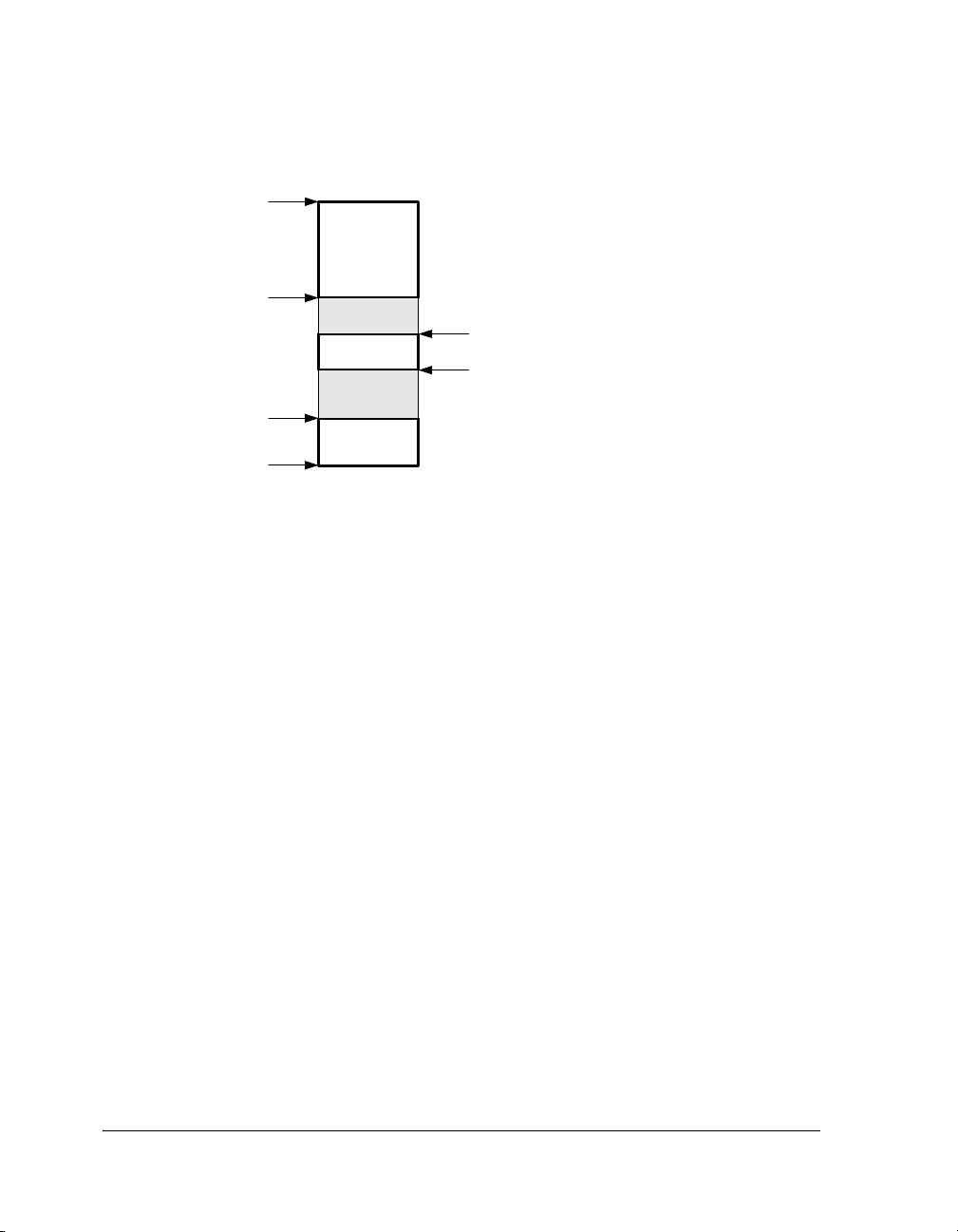
When removing the EZ-KIT Lite board from the package, handle the board carefully to avoid the discharge of static electricity, which may damage the board components. Figure 1-1 shows the default jumper settings, switches, connector locations, and LEDs used in installation. Confirm that your board is set up in the default configuration before powering the board.
ADSP-BF535 EZ-KIT Lite Evaluation System Manual 1-3
Page 26

Default Configuration
Figure 1-1. EZ-KIT Lite Hardware Setup
1-4 ADSP-BF535 EZ-KIT Lite Evaluation System Manual
Page 27

Using ADSP-BF535 EZ-KIT Lite
Installation and Session Startup
L
For correct operation, install the software and hardware in the order presented in the VisualDSP++ Installation Quick Reference Card.
1. Verify that the yellow USB monitor LED ( USB connector) is lit. This signifies that the board is communicating properly with the host PC and is ready to run VisualDSP++.
2. If you are running VisualDSP++ for the first time, navigate to the VisualDSP++ environment via the Start –> Programs menu. The main window appears. Note that VisualDSP++ does not connect to any session. Skip the rest of this step to step 3.
If you have run VisualDSP++ previously, the last opened session appears on the screen. You can override the default behavior and force VisualDSP++ to start a new session by pressing and holding down the Ctrl key while starting VisualDSP++. Do not release the Ctrl key until the Session Wizard appears on the screen. Go to step 4.
3. To connect to a new EZ-KIT Lite session, start Session Wizard by selecting one of the following.
LED5, located near the
• From the Session menu, New Session.
• From the Session menu, Session List. Then click New Ses- sion from the Session List dialog box.
• From the Session menu, Connect to Target. Then click New Session from the Session List dialog box.
4. The Select Processor page of the wizard appears on the screen. Ensure Blackfin is selected in Processor family. In Choose a target processor, select ADSP-BF535. Click Next.
ADSP-BF535 EZ-KIT Lite Evaluation System Manual 1-5
Page 28

Installation and Session Startup
5. The Select Connection Type page of the wizard appears on the screen. Select EZ-KIT Lite and click Next.
6. The Select Platform page of the wizard appears on the screen. In the Select your platform list, select ADSP-BF535 EZ-KIT Lite via Debug Agent. In Session name, highlight or specify the session name.
The session name can be a string of any length; although, the box
displays approximately 32 characters. The session name can
include space characters. If you do not specify a session name,
VisualDSP++ creates a session name by combining the name of the
selected platform with the selected processor. The only way to
change a session name later is to delete the session and to open a
new session.
Click Next.
7. The Finish page of the wizard appears on the screen. The page dis- plays your selections. If you are satisfied, click Finish. If not, click Back to make changes.
L
1-6 ADSP-BF535 EZ-KIT Lite Evaluation System Manual
To disconnect from a session, click the disconnect button
or select Session –> Disconnect from Target.
To delete a session, select Session –> Session List. Select the ses- sion name from the list and click Delete. Click OK.
Page 29

Using ADSP-BF535 EZ-KIT Lite
Evaluation License Restrictions
The ADSP-BF535 EZ-KIT Lite installation is part of the VisualDSP++
installation. The EZ-KIT Lite is a licensed product that offers an unrestricted evaluation license for the first 90 days. Once the initial
unrestricted 90-day evaluation license expires:
• VisualDSP++ allows a connection to the ADSP-BF535 EZ-KIT
Lite via the USB Debug Agent interface only. Connections to simulators and emulation products are no longer allowed.
• The linker restricts a users program to 176 KB of internal memory
for code space with no restrictions for data space.
L
Refer to the VisualDSP++ Installation Quick Reference Card for details.
The EZ-KIT Lite hardware must be connected and powered up in order to use VisualDSP++ with a valid temporary or demo license.
Memory Map
The ADSP-BF535 processor has internal SRAM that can be used for instruction or data storage. The configuration of internal SRAM is detailed in the ADSP-BF535 Processor Hardware Reference.
The ADSP-BF535 EZ-KIT Lite board contains 272K x 16 bits of external
flash memory. This memory connects to the
the processor. The external memory also connects to 4M x 32-bit SDRAM
memory. This memory connects to the
~AMS0 memory select pin of
~SMS0 pin of the processor.
ADSP-BF535 EZ-KIT Lite Evaluation System Manual 1-7
Page 30

SDRAM Interface
Table 1-1. EZ-KIT Lite Evaluation Board Memory Map
Start Address End Address Content
External Memory
Internal Memory
0x0000 0000 0x00FF FFFF SDRAM bank 0 (SDRAM)
See “SDRAM Interface” on page 1-8.
0x2000 0000 0x2009 FFFF ASYNC memory bank 0 (flash memory)
See “Flash Memory” on page 1-9.
All other locations Not used
0xF000 0000 0xF003 FFFF L2 SRAM 256 KB
0xFF80 0000 0xFF80 3FFF Data bank A 16 KB
0xFF90 0000 0xFF90 3FFF
0xFFA0 0000 0xFFA0 3FFF
0xFFB0 0000 0xFFB0 0FFF
0xFFC0 0000 0xFFDF FFFF
0xFFE0 0000 0xFFFF FFFF Core MMRs 2 MB
All other locations Reserved
Data bank B 16 KB
Instruction SRAM 16 KB
Scratch pad SRAM 4 KB
System MMRs 2 MB
SDRAM Interface
In order to use the 4M x 32 bits (16 MB) of SDRAM memory, the three SDRAM control registers must be initialized. Table 1-2 shows the standard configuration for these registers when using the EZ-KIT Lite in the default configuration. These numbers were derived using the M48LC4M16ATG-75 with a system clock frequency of 120 MHz.
If you are in an EZ-Kit Lite or emulator session, the SDRAM registers are set to the values in Table 1-2 automatically when a reset operation is per- formed. Clearing the Use XML reset values check box on the Target Options dialog box, which is accessible through the Settings pull-down menu, disables this feature. For more information see the online Help.
1-8 ADSP-BF535 EZ-KIT Lite Evaluation System Manual
Page 31

Table 1-2. SDRAM Default Settings
Register Value Function
EBIU_SDRRC 0x0000074A
RDIV
Using ADSP-BF535 EZ-KIT Lite
= 1866 clock cycles
EBIU_SDBCTL 0x00000001
EBIU_SDGCTL 0x0091998F
Bank 0 enabled
Bank 0 size = 16 MB
Bank 0 column address width = 8 bits
32-bit data path External buffering timing disabled
= 2 SCLK cycles
t
WR
= 3 SCLK cycles
t
RCD
= 3 SCLK cycles
t
RP
t
= 6 SCLK cycles
RAS
pre-fetch disabled
CAS latency = 3
SCLK1 disabled
SCLK cycles
An example program is included in the EZ-KIT installation directory to demonstrate the SDRAM interface setup.
Flash Memory
The DSM2150 Flash/PLD chip provides a total of 272K x 16 bits of external flash memory, arranged into two independent flash arrays (boot and main). The chip also has a series of configuration registers to control IO and PLD. The chip is initially configured with the memory sectors mapped to the processor, as shown in Figure 1-2.
Use PSDsoft Express™ to modify the default settings of the flash memory. The DSM project must be modified and the flash memory must be
reprogrammed using FlashLINK. The default project files can be found in
…\Blackfin\EZ-KITs\ADSP-BF535\PSDConfigFiles. Analog Devices does
not provide any support for setting up the DSM2150 with PSDsoft
Express or programming it using FlashLINK. E-mail STMicroelectronics
at
apps.psd@st.com for technical assistance.
ADSP-BF535 EZ-KIT Lite Evaluation System Manual 1-9
Page 32
Flash Memory
0x200A 0000
Main Flash
Array
0x2002 0000
0x2000 8000
0x2000 0000
Empty
0x2001 00FF
Config
0x2001 0000
Empty
Boot Flash
Array
Figure 1-2. Flash Memory Map
To program the flash memory with your boot code, first create a loader file from your processor code. Set up the loader in VisualDSP++ depending on how you plan to boot the flash memory. The two possibilities are to boot the processor in 16-bit external execution mode or in 8-bit boot mode. See “Boot Mode Select Switch (SW1)” on page 2-7 for the boot mode settings.
Next, the loader file must be programmed into the flash memory. This can be done through the processor using the VisualDSP++ Flash Programmer utility (see “Flash Programmer Utility” on page 1-13) or by using the FlashLink programmer.
The DSM2150 can be re-programmed using the FlashLINK JTAG programming cable available from STMicroelectronics (
www.st.com/psd) for
approximately $59. FlashLINK plugs into any PC parallel port. The software development tool, PSDsoft Express, is required to modify the
DSM2150 configuration and to operate the FlashLINK cable. PSDsoft
Express can be downloaded at no charge from at
www.st.com/psd.
1-10 ADSP-BF535 EZ-KIT Lite Evaluation System Manual
Page 33

Using ADSP-BF535 EZ-KIT Lite
Programmable Flag Pins
The ADSP-BF535 processor has 16 asynchronous programmable flag (PF) IO pins. During reset, processor. They are not valid until 120 us after reset. Table 1-3 describes how the PFs can be used after reset.
Table 1-3. Programmable Flag Pin Summary
Flag Connects To Description
PF0 LED4 PF3-0 connect to the LEDs. These can be used to light an LED
PF1 LED1
PF2 LED2
PF3 LED3
PF9-0 function as inputs to the internal PLL of the
when a routine completes.
PF4 SW4 PF7-4
PF5 SW5
PF6 SW6
PF7 SW7
PF8
PF9 Not used
PF10 Not used
PF11 Not used
PF12 PMGMT0 These are used to change the internal voltage of the processor.
PF13 PMGMT1
PF14 PMGMT2
PF15 U7.11
connect to the push buttons on the EZ-KIT Lite board
and are for user input. Your routine can monitor and execute
specific code when a push button is pressed.
Not used
Refer to “Power Management” on page 1-12 for more information.
Connects to the reset signal of the AD1885 codec (U7). This signal must be output as a high (
1) to enable the AD1885 codec.
ADSP-BF535 EZ-KIT Lite Evaluation System Manual 1-11
Page 34

Programmable Flag Pins
After a processor reset, all of the PF pins are initialized as inputs. The
direction of the PF is configured by the
(MMR). The PFs are set high (
using the
FIO_FLAG_C MMRs. For more information on configuring the
1) using the FIO_FLAG_S and cleared (0)
FIO_DIR memory mapped register
PF pins, see the ADSP-BF535 Processor Hardware Reference Manual.
All of the PFs can are brought out to the expansion connector
P2. The
location of the PF nets can be found in “ADSP-BF535 EZ-KIT Lite Sche-
matic” on page B-1.
Power Management
The PF14–12 pins allow you to program the core voltage of the processor. The default core voltage is 1.5V. Table 1-4 shows the voltage values and corresponding states of the
Table 1-4. Power Settings
PF14 Pin PF13 Pin PF12 Pin VDD_INT Pin
0 0 0 0.9V
0 0 1 1.0V
0 1 0 1.1V
0 1 1 1.2V
1 0 0 1.3V
1 0 1 1.4V
1
1
10 1.5V
PF14–12 pins.
1 1 1 1.6V
1 Default settings
When lowering the core voltage of the processor, the frequency of the processor must also be taken into consideration. As you lower the core
voltage, the frequency at which the core is running must be decreased.
1-12 ADSP-BF535 EZ-KIT Lite Evaluation System Manual
Page 35

Using ADSP-BF535 EZ-KIT Lite
Example Programs
Example programs are provided with the ADSP-BF535 EZ-KIT Lite to demonstrate various capabilities of the evaluation board. These programs are installed with the EZ-KIT Lite software and can be found in the
…\Blackfin\Examples\ADSP-BF535 EZ-KIT Lite subdirectory of the Visu-
alDSP++ installation directory. Please refer to the readme file provided
with each example for more information.
Flash Programmer Utility
The ADSP-BF535 EZ-KIT Lite evaluation system includes a Flash Programmer utility. The utility allows you to program the flash memory on the EZ-KIT Lite. The Flash Programmer is installed with VisualDSP++. Once the utility is installed, it is accessible from the Tools pull-down menu.
For more information on the Flash Programmer utility, refer to online Help.
Background Telemetry Channel
The ADSP-BF535 USB debug agent supports the background telemetry channel (BTC), which facilitates data exchange between VisualDSP++ and the processor without interrupting processor execution.
The BTC allows the user to view a variable as it is updated or changed, all
while the processor continues to execute. For increased performance of the
BTC, including faster reading and writing, please check out our latest line
of processor emulators at
http://www.analog.com/processors/resources/crosscore/emulators/index.html
ADSP-BF535 EZ-KIT Lite Evaluation System Manual 1-13
.
Page 36

Background Telemetry Channel
For more information about the background telemetry channel, see the VisualDSP++ User’s Guide or online Help.
1-14 ADSP-BF535 EZ-KIT Lite Evaluation System Manual
Page 37

2 ADSP-BF535 EZ-KIT LITE
HARDWARE REFERENCE
This chapter describes the hardware design of the ADSP-BF535 EZ-KIT Lite board. The following topics are covered.
• “System Architecture” on page 2-2
Describes the configuration of the ADSP-BF535 (formerly
ADSP-21535) processor and explains how the board components
interface with the processor.
• “Jumper and Switch Settings” on page 2-5
Shows the location and describes the function of the configuration
jumpers and switches.
• “LEDs and Push Buttons” on page 2-9
Shows the location and describes the function of the LEDs and
push buttons.
• “Connectors” on page 2-12
Shows the location and gives the part number for all of the connectors on the board. Also, the manufacturer and part number
information is given for the mating parts.
• “Specifications” on page 2-15
Gives the requirements for powering the board.
ADSP-BF535 EZ-KIT Lite Evaluation System Manual 2-1
Page 38

System Architecture
System Architecture
This section describes the processor’s configuration on the EZ-KIT Lite board.
SPI 1:0
UART1 :0
Timer2:0
SPORT1
USB
PF15:0SPORT0
4M X 32bit
SDRAM
(U5, U6)
SPORT0
Connector
Stereo LINE IN/
MIC and
LINEOUT
Connectors
Expansion
Connectors
(P1, P2, P3)
LEDs, PBs
and Clock
Logic
USB Connector
+7.5V
Connector
SRAM
Oscillator
32.768KHz
Power
Management
5V
A5V 3.3V
Power
Regulation
JTAG Header
EZ USB FX
20MHz
Crystal
3.3V
544KB Flash
(U4)
External Bus Interface
Unit
JTAG Port
ADSP-BF535
RTC
processor
(U1)
CLK_IN
VDD_INT
VDD_EXT
AD1885
Codec
(U7)
Figure 2-1. System Architecture
This EZ-KIT Lite has been designed to demonstrate the capabilities of the ADSP-BF535 Blackfin processor. The processor has a default core voltage of 1.5V. Refer to “Power Management” on page 1-12 for more information about changing the core voltage without halting the processor. The voltage of the processor’s peripheral interface is 3.3V.
A 20 MHz oscillator supplies the input clock to the processor. The speed
at which the core and peripherals operate is determined by the configuration of the multiplier select switch (
SW2) at reset (see “Processor PLL Setup
2-2 ADSP-BF535 EZ-KIT Lite Evaluation System Manual
Page 39

ADSP-BF535 EZ-KIT Lite Hardware Reference
Switch (SW2)” on page 2-7). By default, the processor core runs at
300 MHz, and the peripheral interface runs at 120 MHz. A 32.768 kHz
crystal supplies the real-time clock (RTC) inputs of the processor.
The EZ-KIT Lite board can be configured to boot in all possible ADSP-BF535 boot modes. For information about configuring the boot mode, see “Boot Mode Select Switch (SW1)” on page 2-7.
External Bus Interface
The external bus interface unit (EBIU) connects to 4M x 32 bits of
SDRAM (16 MB). The SDRAM memory connects to the synchronous
memory select 0 (
for information about configuring the SDRAM.
The EBIU also connects to 272K x 16 bits of flash memory. The flash memory connects to the asynchronous memory select ( processor can use this memory for both booting and storing information during normal operation. Refer to “Flash Memory” on page 1-9 for information about using the flash memory.
~SMS0) pin. Refer to “SDRAM Interface” on page 1-8
~AMS0) pin. The
All of the address, data, and control signals are available externally via the extender connectors (
P1-3). The pinout of these connectors can be found
in “ADSP-BF535 EZ-KIT Lite Schematic” on page B-1.
SPORT0 Audio Interface
SPORT0 connects to the AD1885 SoundMAX codec (U7). Two 3.5 mm ste-
reo jacks (P5 and P6) allow audio to be input and output. You can supply
an audio input to the codec microphone input channel (
stereo input channel (
channel driven by the input jack (
LINE_IN). The JP1 settings determine the codec
P5). See “Audio Input Select Jumper
(JP1)” on page 2-5.
ADSP-BF535 EZ-KIT Lite Evaluation System Manual 2-3
MIC1) or to the
Page 40

System Architecture
SPORT0 is routed also to an off-board connector (P9). When using the
off-board connector, the codec must be held in reset not to drive any of
the
SPORT0 signals. The codec can be held in reset by driving PF15 low or
by setting
page 2-6).
JP2 as described in “Audio Codec Disable Jumper (JP2)” on
PF15 must be pulled high (1) for the codec to function.
[
TCLK0 and RCLK0 pins are shorted together using R114 and R118.
Expansion Interface
The expansion interface consists of the footprints for three connectors.
Table 2-1 lists the interfaces each connector provides. For the exact pinout
of the connectors, refer to “ADSP-BF535 EZ-KIT Lite Schematic” on
page B-1. Analog Devices does not populate the expansion connectors or
provide any additional support for the interface. The mechanical locations
of the expansion connectors can be found in “Mechanical Dimensions” on
page 2-17.
Table 2-1. Expansion Connector Interfaces
Connector Interfaces
P1 5V, GND, address, data
P2 3.3V, GND, EBUI control signals, PF15-0, SPI1-0, SPORT1, UART1-0,
TMR2-0, NMI
P3 1.5V, GND, reset, USB, CLKOUT, SLEEP
Limits to the current and to the interface speed must be taken into consideration when using the expansion interface. The maximum current limit is
dependent on the capabilities of the used regulator. Additional circuitry
can also add extra loading to signals, decreasing their maximum effective
speed.
[
effects of additional circuitry.
2-4 ADSP-BF535 EZ-KIT Lite Evaluation System Manual
Analog Devices does not support and is not responsible for the
Page 41

ADSP-BF535 EZ-KIT Lite Hardware Reference
JTAG Emulation Port
The JTAG emulation port allows an emulator to access the processor’s internal and external memories through a 6-pin interface. The JTAG emulation port of the processor also connects to the USB debugging interface. (Note that this is not the processor’s USB interface.) When an emulator connects to the board at abled. See “JTAG (P8)” on page 2-14 for more information.
To learn more about available emulators, contact Analog Devices (see
“Product Information”).
P8, the USB debugging interface is dis-
Jumper and Switch Settings
This section describes the function of the board’s jumpers and switches.
Figure 2-2 on page 2-6 shows the location of the jumpers and switches.
Figure 2-2. Jumper Locations
ADSP-BF535 EZ-KIT Lite Evaluation System Manual 2-5
Page 42

Jumper and Switch Settings
Audio Input Select Jumper (JP1)
The audio input jack (P5) can connect to the MIC1 and LINE_IN input channels of the AD1885 codec ( and 3 and pins 2 and 4,
P5 connects to the mono MIC1 codec channel.
When the jumpers connect pins 3 and 5 and pins 4 and 6,
the stereo
LINE_IN codec channel. These jumper settings are illustrated in
Figure 2-2 on page 2-6. The words
reference.
Table 2-2. Audio Input Jumper Settings (JP1)
Stereo LINE_IN (Default) Mono MIC1
U7). When the JP1 jumpers connect pins 1
P5 connects to
MIC and LINE_IN are on the board as a
JP1
MIC
2
1
LINE
6
5
JP1
MIC
2
1
LINE
6
5
Audio Codec Disable Jumper (JP2)
Placing a jumper between pins 1 and 2 of JP2 holds the AD1885 codec in reset, preventing it from driving signals to the serial port. When a jumper is between pins 2 and 3 of
PF15 is set to an output and is asserted. These positions are labeled on the
board as
DIS and ENA 1885.
JP2, the AD1885 codec is held in reset until
Boot Mode Select Switch (SW1)
The boot mode select switch (SW1) determines how the processor boots.
Table 2-3 shows the switch settings.
SPI ROM is not available on the EZ-KIT Lite.
L
2-6 ADSP-BF535 EZ-KIT Lite Evaluation System Manual
Page 43

ADSP-BF535 EZ-KIT Lite Hardware Reference
Table 2-3. Boot Mode Select Switch
BMODE0
Pin 1
On On On Execute from 16 bit external memory (no-boot)
1
Off
On Off On Boot from SPI0 ROM (8-bit addresses)
Off Off On Boot from SPI0 ROM (16-bit addresses)
– – Off All others reserved
1 Default settings
BMODE1
Pin 2
On On Boot from 8-bit EPROM
BMODE2
Pin 3
Description
Processor PLL Setup Switch (SW2)
The phase lock loop (PLL) of the processor multiplies the 20 MHz input
clock by a multiplication factor to set the core clock speed of the processor. Internal to the processor programmable flag pins
multiplexed with the PLL setup signals
During reset, the function of the
time, the signals are attached to the
external clock speeds of the processor. The
SSEL1-0, DF, and MSEL6-0.
PF9-0 pins is to setup the PLL. At this
SW2 switch to determine the core and
SW2 switch drives the processor
pins during reset and, for approximately 120 ms, after reset. Once this
time has elapsed, the PFs no longer connect to
SW2 but connect to the gen-
eral-purpose IO (LEDs, push buttons) on the board. This is done with an
external 2-to-1 multiplexer to add flexibility to the EZ-KIT Lite.
PF9-0 are
The following table shows each switch position and corresponding processor pin.
ADSP-BF535 EZ-KIT Lite Evaluation System Manual 2-7
Page 44
Jumper and Switch Settings
Table 2-4. PLL Setup Switch (SW2) Functions
Processor Pin Switch Position Processor Pin Switch Position
MSEL0 1 MSEL6 7
MSEL1 2 DF 8
MSEL2 3 SSEL0 9
MSEL3 4 SSEL1 10
MSEL4 5None11
MSEL5 6Bypass12
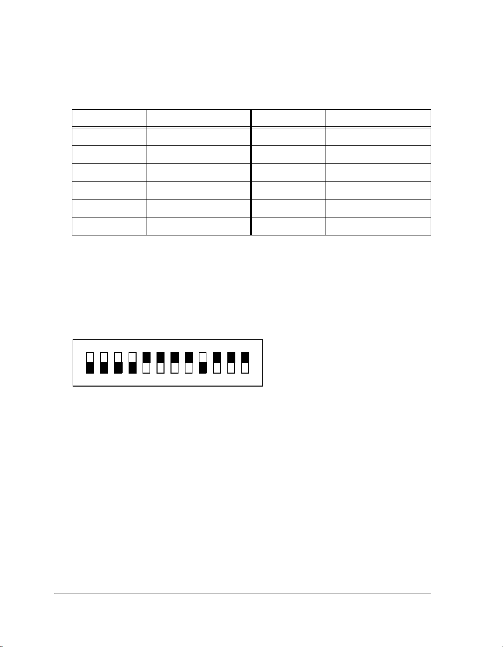
Figure 2-3 shows the default setting of the
SW2 switch. The setting pro-
duces a 300 MHz core clock speed and a 120 MHz peripheral interface
speed. For more information about setting up the multiplication factors,
refer to “Managing DSP Clocks” section of the ADSP-BF535 Processor
Hardware Reference.
ON
1 2 3 4 5 6 7 8 9 10 11 12
Figure 2-3. Default PLL Setup Switch Setting (SW2)
A switch setting of ON supplies a logic low (0) on the corresponding
L
processor pin.
2-8 ADSP-BF535 EZ-KIT Lite Evaluation System Manual
Page 45

ADSP-BF535 EZ-KIT Lite Hardware Reference
LEDs and Push Buttons
This section describes the functionality of the LEDs and push buttons.
Figure 2-4 shows the locations of the LEDs and push buttons.
Figure 2-4. LED and Push Button Locations
Programmable Flag LEDs (LED1–4)
Four LEDs connect to four programmable flag (PF) pins, PF3-0, of the processor. These LEDs are active high and are lit by an output of the processor. Refer to “Programmable Flag Pins” on page 1-11 for information about PF programming.
ADSP-BF535 EZ-KIT Lite Evaluation System Manual 2-9
1 from
Page 46

LEDs and Push Buttons
Table 2-5. Programmable Flag LEDs
LED Reference Designator Processor Programmable Flag Pin
LED4 PF0
LED1 PF1
LED2 PF2
LED3 PF3
USB Monitor LED (LED5)
The USB monitor LED (LED5) indicates that USB communication has been initialized successfully, and you can connect to the processor using a VisualDSP++ EZ-KIT Lite session. This takes approximately 15 seconds. If the LED does not light, try cycling power on the board and/or reinstalling the USB driver (see the VisualDSP++ Installation Quick Reference Card).
L
Lite target board, the LED can flicker, indicating communications
handshake.
Power LED (LED6)
When VisualDSP++ is communicating actively with the EZ-KIT
When LED6 is lit (green), it indicates that power is being supplied to the board properly.
Reset LEDs (LED7 and LED8)
When LED8 is lit, it indicates that master reset of all the major ICs is active. When USB chips reset only on power-up, or if USB communication has not been initialized.
2-10 ADSP-BF535 EZ-KIT Lite Evaluation System Manual
LED7 is lit, the USB interface chip (U11) is being reset. The
Page 47

ADSP-BF535 EZ-KIT Lite Hardware Reference
Non-Maskable Interrupt Push Button (SW3)
The SW3 button connects to the non-maskable interrupt (NMI) pin of the
processor. When pressed, the processor vectors to the NMI vector.
Programmable Flag Push Buttons (SW4–7)
Four push buttons are provided for general-purpose user input. SW4–7 connect to the processor’s programmable flag pins tons are active high and, when pressed, send a high ( Refer to “Programmable Flag Pins” on page 1-11 for information about PF programming. Table 2-6 lists each push button and corresponding programmable flag pin.
Table 2-6. Programmable Flag Switches
Push Button Reference Designator Processor Programmable Flag Pin
PF7-4. The push but-
1) to the processor.
SW4 PF4
SW5 PF5
SW6 PF6
SW7 PF7
Reset Push Button (SW8)
The RESET push button resets all of the ICs on the board. This reset does not affect the USB interface chip ( been initialized with a PC. After USB communication has been initialized, the only way to reset the USB is by powering down the board.
ADSP-BF535 EZ-KIT Lite Evaluation System Manual 2-11
U11) unless communication has not
Page 48

Connectors
Connectors
This section describes the connector functionality and provides information about mating connectors. The connector locations are shown in
Figure 2-5.
Figure 2-5. Connector Locations
Expansion Interface (P1–3)
Three board-to-board connector footprints provide signals for most
peripheral interfaces of the processor. Analog Devices does not populate
the expansion connectors and does not provide any additional support for
the interface. For more information, see “Expansion Interface” on
page 2-4. Contact Samtec for the connector availability and pricing.
2-12 ADSP-BF535 EZ-KIT Lite Evaluation System Manual
Page 49

ADSP-BF535 EZ-KIT Lite Hardware Reference
Part Description Manufacturer Part Number
90-position 0.05” spacing (P1,
P2, P3)
90-position 0.05” spacing (through hole)
90-position 0.05” spacing (surface mount)
90-position 0.05” spacing (low cost)
SAMTEC SFM-145-01-S-D
Mating Connectors
SAMTEC TFM-145-x1 series
SAMTEC TFM-145-x2 series
SAMTEC TFC-145 series
FlashLINK (P4)
The FlashLINK connector allows you to configure and program the STMicroelectronics DSM2150 flash/PLD chip. See “Flash Memory” on
page 1-9 for more information.
Part Description Manufacturer Part Number
Right-angle 7X2 shrouded 0.1” spacing
TYCO 2-767004-2
Mating Assembly
FlashLINK JTAG programmer ST MICRO L-101B
ADSP-BF535 EZ-KIT Lite Evaluation System Manual 2-13
Page 50

Connectors
Audio (P5 and P6)
There are two 3.5 mm stereo audio jacks: one input and one output.
Part Description Manufacturer Part Number
3.5 mm stereo jack (P5, P6) SHOGYO SJ-0359AM-5
Mating Cable
3.5 mm stereo plug to 3.5 mm stereo cable
RADIO SHACK 42-2387A
USB (P7)
The USB connector is a standard type B USB receptacle. The connector is used to debug the processor and is not connected to the processor’s USB interface.
Part Description Manufacturer Part Number
Type B USB receptacle (
USB cable (provided with kit) ASSMANN AK672-5
P7) MILL-MAX 897-30-004-90-000
DIGI-KEY ED90003-ND
Mating Connector
DIGI-KEY AK672-5ND
2-14 ADSP-BF535 EZ-KIT Lite Evaluation System Manual
Page 51

ADSP-BF535 EZ-KIT Lite Hardware Reference
JTAG (P8)
The JTAG header is the connecting point for a JTAG in-circuit emulator pod. When an emulator connects to the JTAG header, the USB debug interface is disabled.
L
should have a plug.
When using an emulator with the EZ-KIT Lite board, follow the
Pin 3 is missing to provide keying. Pin 3 in the mating connector
L
connection instructions provided with the emulator.
SPORT0 (P9)
SPORT0 connects to a 20-pin connector. The pinout of the connector can
be found in “ADSP-BF535 EZ-KIT Lite Schematic” on page B-1. Contact AMP for the connector availability and pricing.
Part Description Manufacturer Part Number
20-position AMPMODU system 50 receptacle (
20-position AMPMODU ribbon cable connector
P9)
AMP 104069-1
Mating Connector
AMP 111196-4
Power Connector (P10)
The power connector provides all of the power necessary to operate the EZ-KIT Lite board.
Part Description Manufacturer Part Number
2.5 mm power jack (
P10) SWITCHCRAFT RAPC712
DIGI-KEY SC1152-ND
ADSP-BF535 EZ-KIT Lite Evaluation System Manual 2-15
Page 52

Specifications
Part Description Manufacturer Part Number
Mating Power Supply (shipped with EZ-KIT Lite)
7.5V power supply GLOBTEK TR9CC2000LCP-Y
Specifications
This section provides the requirements for powering the board and the mechanical dimensions of the board.
Power Supply
The power connector supplies DC power to the EZ-KIT Lite board.
Table 2-7 shows the connector pinout.
Table 2-7. Power Connectors
Terminal Connection
Center pin +7.5 VDC@2amps
Outer ring GND
Board Current Measurements
The ADSP-BF535 EZ-KIT Lite board provides eight zero-ohm resistors that can be removed to measure current draw. Table 2-8 lists and describes each resistor and the voltage plane on the board.
Table 2-8. Current Resistor Measurements
Resistor Voltage Plane Description
R2 VDD_RTC Processor real-time clock supply
R3 VDD_EXT Processor external interface supply
2-16 ADSP-BF535 EZ-KIT Lite Evaluation System Manual
Page 53

ADSP-BF535 EZ-KIT Lite Hardware Reference
Table 2-8. Current Resistor Measurements (Cont’d)
Resistor Voltage Plane Description
R6 VDD_INT Processor internal interface supply
R7 VDD_PCIEXT Processor PCI interface supply
R8 VDD_PLL Processor phase lock loop supply
R110 5V 5V supply
R111 3V 3V supply to all non processor-related components
R113 3V_DSP 3V to processor-related components
Mechanical Dimensions
Figure 2-6 shows the location of the mounting holes and PIN1 of each
expansion connector.
5.000
4.750
3.875
2.500
1.125
0.250
0.000
3.750
1.300
0.000
0.250
0.625
3.250
3.600
P1
P2
1.400
P3
6.375
6.750
6.200
7.000
Figure 2-6. Mechanical Drawing
ADSP-BF535 EZ-KIT Lite Evaluation System Manual 2-17
Page 54

Specifications
2-18 ADSP-BF535 EZ-KIT Lite Evaluation System Manual
Page 55

A ADSP-BF535 EZ-KIT LITE BILL
OF MATERIALS
The bill of materials corresponds to “ADSP-BF535 EZ-KIT Lite Sche-
matic” on page B-1. Please check the latest schematic on the Analog
Devices Web site:
http://www.analog.com/Processors/Processors/DevelopmentTools/tec
hnicalLibrary/manuals/DevToolsIndex.html#Evaluation%20Kit%20Manuals
.
Ref. Qty. Description Reference
Designator
2 3 74LVC14A SOIC14
HEX-INVER-SCHMITT
-TRIGGER
3 1 IDT74FCT3244APY
SSOP20
3.3V-OCTAL-BUFFER
4 1 24.576MHZ SMT
OSC005
CRYSTAL
5 1 CY7C64603-128
PQFP128
USB-TX/RX MICROCONTROLLER
6 1 MMBT4401 SOT-23
NPN TRANSISTOR
200MA
7 1 74LVC00AD SOIC14
U9-10, U19 TI 74LVC14AD
U24 IDT IDT74FCT3244APY
Y2 EPSON MA505 24.576M-C2
U11 CYPRESS CY7C64603-128NC
Q1 FAIRCHILD MMBT4401
U13 PHILIPS 74LVC00AD
Manufacturer Part Number
ADSP-BF535 EZ-KIT Lite Evaluation System Manual A-1
Page 56

Ref. Qty. Description Reference
Designator
Manufacturer Part Number
8 1 24LC00-SN SOIC8
128 BIT SERIAL
EEPROM
9 1 ADP3331ART SOT23-6
ADJ 200MA REGULATOR
10 3 BSS123 SOT23D
NMOS FET
11 1 CY7C1019BV33-15VC
SOJ32
128K X 8 SRAM
12 1 SN74AHC1G02
SOT23-5
SINGLE-2 INPUT-NOR
13 1 SN74LV164A SOIC14
8-BIT-PARALLEL-SERIAL
14 1 CY7C4201V-15AC
TQFP32
64-BYTE-FIFO
15 1 12.0MHZ THR OSC006
CRYSTAL
U25 MICROCHIP 24LC00-SN
VR3 ANALOG
ADP3331ART
DEVICES
M1-3 FAIRCHILD BSS123
U12 CYPRESS CY7C1019BV33-
12VC
U16 TI SN74AHC1G02
DBVR
U17 TI SN74LV164AD
U18 CYPRESS CY7C4201V-15AC
Y3 DIG01 300-6027-ND
16 2 MT48LC4M16 TSOP54
4MX16-SDRAM-133M
U5-6 MICRON MT48LC4M16A2
TG-75
HZ
17 1 32.768kHz TH OSC007
Y1 ECPLITEK EC38T
CRYSTAL
18 1 SN74AHC1G00
SOT23-5 SINGLE-2-
U26 TI SN74AHC1G00
DBVR
INPUT-NAND
19 1 21535 DSM2150F5V
U4 ST MICRO DSM2150F5V
“U4”
A-2 ADSP-BF535 EZ-KIT Lite Evaluation System Manual
Page 57

ADSP-BF535 EZ-KIT Lite Bill Of Materials
Ref. Qty. Description Reference
Designator
20 2 1000pF 50V 5% 1206
C25-26 AVX 12065A102JAT2A
CERM
21 2 0.1uF 50V 10% 1206
C8-9 PHILIPS 12062R104K9BB2
CERM
22 1 ADM708SAR SOIC8
U23 ANALOG
VOLTAGE-SUPERVISOR
23 1 AD1885JST LQFP48
U7 ANALOG
AC97 STEREO CODEC
24 2 ADP3338AKC-33
VR1-2 ANALOG
SOT-223
3.3V-1.0AMP REGULATOR
25 1 ADP3339AKC-5
VR4 ANALOG
SOT-223
5V-1.5A REGULATOR
26 1 ADP3088 MSOP8
VR5 ANALOG
500MA-BUCK-REGULATOR
27 1 ADSP-21535PKB-300
U1 ANALOG
PBGA260
308KBYTES-BLACKFIN
Manufacturer Part Number
ADM708SAR
DEVICES
AD1885JST
DEVICES
ADP3338AKC-3.3
DEVICES
ADP3339AKC-5-
DEVICES
REEL
ADP3088ARM-REEL
DEVICES
ADSP-21535PKB-300
DEVICES
28 5 RUBBER FEET BLACK
29 1 PWR 2.5MM_JACK
CON005 RA
30 1 USB 4PIN CON009
USB
31 1 .05 10X2 CON014
MH1-5 MOUSER 517-SJ-5018BK
P10 SWITCH-
SC1152-ND12
CRAFT
P7 MILL-MAX 897-30-004-90-
000000
P9 AMP 104069-1
RA
32 6 SPST-MOMENTARY
SW3-8 PANASONIC EVQ-PAD04M
SWT013 6MM
33 1 DIP12 SWT014
SW2 DIGI-KEY CKN3063-ND
ADSP-BF535 EZ-KIT Lite Evaluation System Manual A-3
Page 58

Ref. Qty. Description Reference
Manufacturer Part Number
Designator
34 1 DIP3 SWT015 SW1 DIGI-KEY CKN3055-ND
35 1 IDC 7X2
IDC7X2SRDRA
RIGHT ANGLE
SHROUDED
36 23 0.00 1/8W 5% 1206
37 2 220uF 10V 20% E
ELEC
38 5 AMBER-SMT LED001
GULL-WING
39 2 22pF 50V 5% 805
CERM
40 79 0.01uF 100V 10% 805
CERM
41 1 0.22uF 25V 10% 805
CERM
42 5 0.1uF 50V 10% 805
CERM
43 4 10uF 16V 10% C
TANT
P4 MOLEX 70247-1401
R2-3, R6-12,
R21,R63-64,
R77, R97,
R111-118, R127
CT7-8 SPRAGUE 293D227X9010E2T
LED1-5 PANASONIC LN1461C-TR
C5-C6 AVX 08055A220JAT
C19, C30-92,
C94, C96-97,
C99-109, C116
C114 AVX 08053C224FAT
C3, C24, C27-29 AVX 08055C104KAT
CT15-18 SPRAGUE 293D106X9025C2T
YAGEO 0.0ECT-ND
AVX 08051C103KAT2A
44 44 10K 100MW 5% 805
45 44 10K 100MW 5% 805 R83-84, R87-88,
R1, R13-19,
R31-32, R37,
R44-45, R47-54,
R57, R59-61,
R66, R68,
R78-81
R90-93, R105,
R120-122, R125
AVX CR21-103J-T
DALE CRCW0805-103JRT1
A-4 ADSP-BF535 EZ-KIT Lite Evaluation System Manual
Page 59

ADSP-BF535 EZ-KIT Lite Bill Of Materials
Ref. Qty. Description Reference
Manufacturer Part Number
Designator
46 4 33 100MW 5% 805 R4-5, R46, R119 AVX CR21-330JTR
47 5 4.7K 100MW 5% 805 R55-56, R58,
R62, R107
48 1 1M 100MW 5% 805
R41 AVX CR21-1004F-T
AVX CR21-4701F-T
49 1 1.5K 100MW 5% 805 R43 AVX CR21-1501F-T
50 1 22uF 16V 10% D
CT1 DIG01 PCT3226CT-ND
TANT
51 3 2.21K 1/8W 1% 1206
52 4 10uF 16V 10% B
R30, R35, R40 AVX CR32-2211F-T
CT4, CT19-21 AVX TAJB106K016R
TANT
53 1 1A HSM160J
DO-214AA
D4 MICRO-
SEMI
HSM160J
SCHOTTKY
54 5 100 100MW 5% 805
55 1 1000 100MHZ 1.5A
R67, R82,
R85-86, R89
FER9 MURATA PLM250S40T1
AVX CR21-101J-T
FER002
0.06 CHOKE
56 3 2A S2A_RECT
DO-214AA
D1-3 GENER-
ALSEMI
S2A
SILICON RECTIFIER
57 8 600 100MHZ 500MA
FER1-8 DIGIKEY 240-1019-1-ND
1206 0.70 BEAD
58 1 0.047UF 16V 10% 1206
C10 AVX 12065C473JATME
59 2 270PF 50V 10% 805 C11, C13 KEMET C1206C271J5GA
C210
60 6 1UF 16V 10% 805
X7R
61 6 470PF 100V 10% 1206
CERM
C4, C22,
C110-113
C12, C14-16,
C20-21
MURATA GRM40X7R105
K016AL
AVX 12061A471JAT2A
ADSP-BF535 EZ-KIT Lite Evaluation System Manual A-5
Page 60

Ref. Qty. Description Reference
Manufacturer Part Number
Designator
62 2 30PF 100V 5% 1206 C17-18 AVX 12061A300JAT2A
63 3 10UF 25V +80-20%
1210 Y5V
64 1 0.47UF 20V 10% A
TANT
65 1 16K 1/8W5% 1206
66 1 53.6K 1/10W 1% 805
67 1 165K 1/10W 1% 805
68 1 316K 1/10W 1% 805
69 1 332K 1/10W 1% 805
70 1 665K 1/10W 1% 805
71 1 10UH 47+/-20 IND001
72 1 243.0K 1/10W 1% 805
73 1 1.00M 1/4W 1% 1210
C93, C95, C98 MURATA GRM235Y.5V106
Z025
CT14 KEMET T491A474K025AS
R65 DALE CRCW1206-163JRT1
R95 PHILIPS 9C08052A5362
FKRT/R
R102 PHILIPS 9C08052A1653
FKRT/R
R103 PHILIPS 9C08052A3163
FKRT/R
R101 PHILIPS 9C08052A3323
FKRT/R
R100 PHILIPS 9C08052A6653
FKRT/R
L1 TDK SLF7045T-
100M1R1-2
R106 PHILIPS 9C08052A2433
FKRT/R
R108 PANASONIC
ERJ-14NF1004U
ECG
74 3 10K 31MW 5% RNET8
75 2 39PF 50V 5% 805
RN6-8 CTS 746X101103J
C1-C2 PANASONIC ECJ-2VC1H390J
NPO
76 5 10K 100MW 2%
RN1-5 CTS 767-161-103G
RNET16 BUSSED
77 1 1K 1/8W 5% 1206
R38 AVX CR32-102J-T
78 6 10K 1/8W 5% 1206 R23-27, R33 DALE CRCW1206-
1002FRT1
A-6 ADSP-BF535 EZ-KIT Lite Evaluation System Manual
Page 61

ADSP-BF535 EZ-KIT Lite Bill Of Materials
Ref. Qty. Description Reference
Manufacturer Part Number
Designator
79 1 100K 1/8W 5% 1206 R109 DALE CR1206-1003FTR1
80 1 20.0K 1/8W 1% 1206 R104 DALE CRCW1206-
2002FRT1
81 3 22 1/8W 5% 1206
R36, R39, R126 DALE CR1206-22R0JTR
82 7 270 1/8W 5% 1206 R69-73, R75-76 AVX CR32-271J-T
83 4 4.7K 1/8W 5% 1206 R20, R22,
R28-29
84 1 680 1/8W 5% 1206
R74 AVX CR32-681J-T
AVX CR32-472J-T
85 1 20MHZ 1/2 OSC001 U2 ECLIPTEK EC1100HS-
20.000MHZ
86 2 RED-SMT LED001
LED7-8 PANASONIC LN1261C
GULL-WING
87 1 GREEN-SMT LED001
LED6 PANASONIC LN1361C
GULL-WING
88 5 1uF 25V 20% A
CT9-13 PANASONIC ECS-T1EY105R
TANT -55+125
89 5 QS3257Q QSOP16
QUICKSWITCH-257
U14-15, U20-22 ANALOG
DEVICES
ADG774ABRQ
90 1 IDC 3X1 IDC3X1
91 1 IDC 3X2 IDC3X2
JP2 BERG 54101-T08-03
JP1 BERG 54102-T08-03
92 1 IDC 7X2 IDC7X2 P8 BERG 54102-T08-07
93 3 IDC 2PIN_JUMPER
SJ1-3 MOLEX 15-38-1024
0.1
94 1 2.5A RESETABLE
FUS001
95 2 3.5MM STEREO_JACK
CON001
F1 RAYCHEM
CORP.
P5-6 A/D ELEC-
TONICS
SMD250-2
ST-323-5
ADSP-BF535 EZ-KIT Lite Evaluation System Manual A-7
Page 62

A-8 ADSP-BF535 EZ-KIT Lite Evaluation System Manual
Page 63

A B C D
1
1
2
2
ADSP-BF535 EZ-KIT LITE
3
ANALOG
4
DEVICES
20 Cotton Road
Nashua, NH 03063
PH: 1-800-ANALOGD
3
4
Approvals Date
Title
ADSP-BF535 EZ-KIT LITE - TITLE
Drawn
Checked
Engineering
A B C D
Size Board No.
C
Date Sheet of
3-12-2003_15:48
A0162-2000
Rev
1.6
1 12
Page 64

A B C D
3V_DSP
R2
0.00
1206
VDD_RTC
PWR_MGT_OUT VDD_INT
R6
0.00
1206
3.3V
FOR RTC
VDD_EXT
R3
1
0.00
1206
R7
0.00
1206
R34
DNP
1206
VDD_PCIEXT
1.5V VDD_PLL
R8
0.00
1206
0 OHM RESISTORS TO MEASURE DSP CURRENT
R1
10K
805
U2
1 5
OE OUT
20MHZ
OSC001
R4
33
805
CLKIN
XTALI XTALO
Y1
XXMHZ
32.768KHZ
OSC007
C2
39PF
805
C1
39PF
805
ARDY
PCI_RST
PCI_CBE0
PCI_CBE1
PCI_CBE2
PCI_CBE3
PCI_GNT
RN1
1
R1
3
R3
4
R4
5
R5
6
R6
7
R7
8 9
R8 R9
10K
RNET16
COM
R15R2
R14
R13
R12
R11
R10
16
152
14
13
12
11
10
3V_DSP
PCI_IRDY
PCI_PAR
PCI_FRAME
PCI_INTD
PCI_INTC
PCI_INTB
PCI_INTAPCI_DEVSEL
PCI_TRDY
PCI_SERR
PCI_PERR
PCI_LOCK
PCI_STOP
PCI_AD31
PCI_AD28
PCI_AD25
RN2
1
R1
2 15
3
R3
4
R4
5
R5
6
R6
7
R7
R8 R9
10K
RNET16
COM
R15R2
R14
R13
R12
R11
R10
16
14
13
12
11
10
98
3V_DSP
PCI_AD21
PCI_AD17
PCI_AD16
PCI_AD11
PCI_AD2
R9
0.00
1206
R10
0.00
1206
R11
0.00
1206
R12
0.00
1206
R77
0.00
1206
R127
0.00
1206
USB_CLK
USB_XVER_DATA
USB_DPLS
USB_DMNS
PCI_CLK
PCI_IDSEL
1
U1
A[25:2]
2
A2
A3
A4
A5
A6
A7
A8
A9
A10
A11
A12
A13
A14
A15
A16
A17
A18
A19
A20
A21
A22
A23
A24
A25
A06
B06
D06
C06
A05
B05
A04
C05
D05
B04
A01
C04
D04
A03
B03
A02
C03
D03
B02
C02
E03
C01
F03
D02
A2
A3
A4
A5
A6
A7
A8
A9
A10
A11
A12
A13
A14
A15
A16
A17
A18
A19
A20
A21
A22
A23
A24
A25
3
R10
XTALI
XTALO
VDD_RTC
VDD_PLL
BYPASS
CLKIN TCK
BMODE0
BMODE1
BMODE2
NMI
SLEEP
RESET
XTALI
T10
XTALO
U10
VDD_RTC
V11
VSS_RTC
G09
VDD_PLL
A10
VSS_PLL
C12
BYPASS
D09
CLKIN1
B14
BMODE0
A14
BMODE1
B13
BMODE2
B11
NMI
D12
SLEEP
B09
RESET
ADSP-BF535PKB-300
PBGA260
D0
D1
D2
D3
D4
D5
D6
D7
D8
D9
D10
D11
D12
D13
D14
D15
D16
D17
D18
D19
D20
D21
D22
D23
D24
D25
D26
D27
D28
D29
D30
D31
TCK
TDI
TDO
TMS
TRST
EMU
N02
M03
T01
P02
N03
R02
P03
U01
U02
T02
V02
V03
R04
U03
T03
T04
U04
V04
V05
R05
T05
U05
V06
R06
U06
T06
V07
V08
U07
R07
T07
V09
D10
C11
D11
A12
B12
A13
D0
D1
D2
D3
D4
D5
D6
D7
D8
D9
D10
D11
D12
D13
D14
D15
D16
D17
D18
D19
D20
D21
D22
D23
D24
D25
D26
D27
D28
D29
D30
D31
TDI
TDO
TMS
TRST
EMU
D[31:0]
SCLK0
CLKOUT
RX0
TX0
RX1
TX1
TMR0
TMR1
TMR2
ARDY
AOE
ARE
AWE
AMS0
AMS1
AMS2
AMS3
~ABE0/SDQM0
~ABE1/SDQM1
~ABE2/SDQM2
~ABE3/SDQM3
SRAS
SCAS
SWE
SMS0
SMS1
SMS2
SMS3
SA10
SCKE
R119
33
805
R5
33
805
U1
A07
RX0
A08
TX0
B08
RX1
C08
TX1
B07
TMR0
C07
TMR1
D07
TMR2
R01
ARDY
E01
AOE
F01
ARE
G01
AWE
F02
AMS0
D01
AMS1
H03
AMS2
G02
AMS3
E02
~ABE0/SDQM0
B01
~ABE1/SDQM1
G03
~ABE2/SDQM2
H07
~ABE3/SDQM3
L02
SRAS
L03
SCAS
J03
SWE
M02
SMS0
P01
SMS1
N01
SMS2
K03
SMS3
M01
SA10
L01
SCKE
K01
SCLK0
H01
CLKOUT/SCLK1
ADSP-BF535PKB-300
PBGA260
RSCLK0
RFS0
DR0
TSCLK0
TFS0
DT0
RSCLK1
RFS1
DR1
TSCLK1
TFS1
DT1
MOSI0
MISO0
SCK0
MOSI1
MISO1
SCK1
MSEL0/PF0
MSEL1/PF1
MSEL2/PF2
MSEL3/PF3
MSEL4/PF4
MSEL5/PF5
MSEL6/PF6
DF/PF7
SSEL0/PF8
SSEL1/PF9
PF10
PF11
PF12
PF13
PF14
PF15
R13
U13
V14
V15
T14
R14
U14
V16
U15
T15
R15
V17
U16
T16
U17
T17
U18
R16
U08
R08
T08
V10
U09
R09
T09
R11
T11
U11
V12
T12
R12
U12
V13
T13
MS_PF0
MS_PF1
MS_PF2
MS_PF3
MS_PF4
MS_PF5
MS_PF6
RCLK0
RFS0
DR0
TCLK0
TFS0
DT0
RCLK1
RFS1
DR1
TCLK1
TFS1
DT1
MOSI0
MISO0
SCK0
MOSI1
MISO1
SCK1
MS_PF[6:0]
DF_PF7
SSEL0_PF8
SSEL1_PF9
PF10
PF11
PF12
PF13
PF14
PF15
PCI_AD0
PCI_AD1
PCI_AD2
PCI_AD3
PCI_AD4
PCI_AD5
PCI_AD6
PCI_AD7
PCI_AD8
PCI_AD9
PCI_AD10
PCI_AD11
PCI_AD12
PCI_AD13
PCI_AD14
PCI_AD15
PCI_AD16
PCI_AD17
PCI_AD18
PCI_AD19
PCI_AD20
PCI_AD21
PCI_AD22
PCI_AD23
PCI_AD24
PCI_AD25
PCI_AD26
PCI_AD27
PCI_AD28
PCI_AD29
PCI_AD30
PCI_AD31
4
U1
E17
PCI_AD0
E18
PCI_AD1
G16
PCI_AD2
F17
PCI_AD3
F18
PCI_AD4
G18
PCI_AD5
G17
PCI_AD6
H18
PCI_AD7
J18
PCI_AD8
H17
PCI_AD9
K18
PCI_AD10
H16
PCI_AD11
L18
PCI_AD12
J17
PCI_AD13
M18
PCI_AD14
K17
PCI_AD15
J16
PCI_AD16
K16
PCI_AD17
N18
PCI_AD18
P18
PCI_AD19
L17
PCI_AD20
L16
PCI_AD21
R18
PCI_AD22
T18
PCI_AD23
M17
PCI_AD24
M16
PCI_AD25
N17
PCI_AD26
P17
PCI_AD27
P15
PCI_AD28
N16
PCI_AD29
R17
PCI_AD30
P16
PCI_AD31
ADSP-BF535PKB-300
PBGA260
PCI_CLK
PCI_RST
PCI_CBE0
PCI_CBE1
PCI_CBE2
PCI_CBE3
PCI_REQ
PCI_GNT
PCI_DEVSEL
PCI_IDSEL
PCI_INTA
PCI_INTB
PCI_INTC
PCI_INTD
PCI_FRAME
PCI_PAR
PCI_IRDY
PCI_TRDY
PCI_SERR
PCI_PERR
PCI_LOCK
PCI_STOP
USB_CLK
XVER_DATA
DPLS
DMNS
TXDPLS
TXDMNS
TXEN
SUSPEND
D14
D18
F16
F15
E16
D17
D16
C18
C16
B18
C14
B15
A15
D13
C17
C15
E15
B17
B16
D15
A16
A17
G07
A09
C09
D08
B10
G10
C10
A11
PCI_CLK
PCI_RST
PCI_CBE0
PCI_CBE1
PCI_CBE2
PCI_CBE3
PCI_GNT
PCI_DEVSEL
PCI_IDSEL
PCI_INTA
PCI_INTB
PCI_INTC
PCI_INTD
PCI_FRAME
PCI_PAR
PCI_IRDY
PCI_TRDY
PCI_SERR
PCI_PERR
PCI_LOCK
PCI_STOP
USB_CLK
USB_XVER_DATA
USB_DPLS
USB_DMNS
USB_TXDLPLS
USB_TXDMNS
USB_TXEN
USB_SUSPEND
ANALOG
DEVICES
3V_DSP
5
10
5
10
5
10
20 Cotton Road
Nashua, NH 03063
PH: 1-800-ANALOGD
RN8
COM1
COM2
10K
RNET8
RN7
COM1
COM2
10K
RNET8
RN6
COM1
COM2
10K
RNET8
R1
R2
R3
R4
R5
R6
R7
R8
R1
R2
R3
R4
R5
R6
R7
R8
R1
R2
R3
R4
R5
R6
R7
R8
1
PCI_AD0
2
PCI_AD1
3
PCI_AD3
4
PCI_AD4
6
PCI_AD9
7
PCI_AD7
8
PCI_AD5
9
PCI_AD6
1
PCI_AD13
2
PCI_AD8
3
PCI_AD10
4
PCI_AD15
6
PCI_AD14
7
PCI_AD24
8
PCI_AD20
9
PCI_AD12
2
3
1
PCI_AD29
2
PCI_AD18
3
PCI_AD26
4
PCI_AD19
6
PCI_AD30
7
PCI_AD23
8
PCI_AD22
9
PCI_AD27
4
Approvals Date
Title
ADSP-BF535 EZ-KIT LITE - DSP
Drawn
Checked
Engineering
A B C D
Size Board No.
C
Date Sheet of
3-25-2003_9:50
A0162-2000
Rev
1.6
2 12
Page 65

A B C D
3.3V 3.3V
1
RN3
R15R2
R14
R13
R12
R11
R10
16
152
14
13
12
11
10
PD0PB1
PD1
PD3
PA0
PA1
PA2
PA3
PA4PB4
PA5
PA6
PA7
PB0
PB2
PB3
PB5
PB6
PB7
1
R1
3
R3
4
R4
5
R5
6
R6
7
R7
8 9
R8 R9
10K
RNET16
2
R13
10K
805
3.3V
3
P4
1
3
5
7
9
11
13
7X2
IDC7X2SRDRA
2
4
6
8
10
12
14
RN4
1
R1COM
3
R3
4
R4
5
R5
6
R6
7
R7
8 9
R8 R9
10K
RNET16
R14
10K 10K
805
COM
R15R2
R14
R13
R12
R11
R10
3.3V
R15 R16
805
16
152
14
13
12
11
10
10K
805
RESET
10K
805
PC7
PE6
PE7
R18R17
10K
805
~ABE0/SDQM0
~ABE3/SDQM3
R19
10K
805
12
13
74LVC00AD
SOIC14
A[21:2]
~ABE1/SDQM1
U13
11
AMS0
PC7
AWE
AOE
PE6
PE7
3 4
74LVC14A
SOIC14
U9
512 KB MAIN FLASH
32KB SECONDARY FLASH
U4
A2
A3
A4
A5
A6
A7
A8
A9
A10
A11
A12
A13
A14
A15
A16
A17
A18
A19
A20
A21
3
AD0
4
AD1
5
AD2
6
AD3
7
AD4
10
AD5
11
AD6
12
AD7
13
AD8
14
AD9
15
AD10
16
AD11
17
AD12
18
AD13
19
AD14
20
AD15
41
PC0
42
PC1
43
PC2
44
PC3
45
PC4
46
PC5
47
PC6
48
PC7
59
CNTL0/~WR
40
CNTL2
71
PE0/TMS
72
PE1/TCK
73
PE2/TDI
74
PE3/TDO
75
PE4/TSTAT
76
PE5/~TERR
78
PE7
39
RESET
DSM2150F5V-12T6
TQFP80
PF0
PF1
PF2
PF3
PF4
PF5
PF6
PF7
PG0
PG1
PG2
PG3
PG4
PG5
PG6
PG7
PA0
PA1
PA2
PA3
PA4
PA5
PA6
PA7
PB0CNTL1/~RD
PB1
PB2
PB3
PB4
PB5
PB6
PB7
PD0PE6
PD1
PD2
PD3
31
D0
32
D1
33
D2
34
D3
35
D4
36
D5
37
D6
38
D7
21
D8
22
D9
23
D10
24
D11
25
D12
26
D13
27
D14
28
D15
51
52
53
54
55
56
57
58
6160
62
63
64
65
66
67
68
7977
80
1
2
PA0
PA1
PA2
PA3
PA4
PA5
PA6
PA7
PB0
PB1
PB2
PB3
PB4
PB5
PB6
PB7
PD0
PD1
SLEEP
PD3
D[15:0]
D[31:0]
A[19:2]
SA10
SWE
SCAS
SRAS
~ABE0/SDQM0
~ABE1/SDQM1
~ABE2/SDQM2
~ABE3/SDQM3
SCLK0
SCKE
SMS0
4M X 16 4M X 16
U5
23
A2
A0
24
A3
A1
25
A4
A2
26
A5
A3
29
A6
A4
30
A7
A5
31
A8
A6
32
A9
A7
33
A10
A8
34
A11
A9
22
A10
35
A13
A11
21
A19
BA1
20
A18
BA0
16
WE
17 19
CAS CS
18
RAS
15
DQML
39
DQMH
MT48LC4M16
TSOP54
DQ0
DQ1
DQ2
DQ3
DQ4
DQ5
DQ6
DQ7
DQ8
DQ9
DQ10
DQ11
DQ12
DQ13
DQ14
DQ15
CKE
CLK
SDRAMSDRAM
U6
2
D0 D16
4
D1
5
D2
7
D3
8
D4
10
D5
11
D6
13
D7
42
D8
44
D9
45
D10
47
D11
48
D12
50
D13
51
D14
53
37
38
A2
23
A0
A3
24
A1
A4
25
A2
A5
26
A3
A6
29
A4
A7
30
A5
A8
31
A6
A9
32
A7
A10
33
A8
A11
34
A9
22
A10
A13
35
A11
A19
21
BA1
A18
20
BA0
16
WE
17 19
CAS CS
18
RAS
15
DQML
39
DQMH
MT48LC4M16
TSOP54
DQ10
DQ11
DQ12
DQ13
DQ14
DQ15
DQ0
DQ1
DQ2
DQ3
DQ4
DQ5
DQ6
DQ7
DQ8
DQ9
CKE
CLK
2
4
D17
5
D18
7
D19
8
D20
10
D21
11
D22
13
D23
42
D24
44
D25
45
D26
47
D27
48
D28
50
D29
51
D30
53
D31D15
37
38
1
2
3
C4C3
0.1UF
805
PSD JTAG HEADER
1UF
805
ANALOG
20 Cotton Road
Nashua, NH 03063
4
Approvals Date
Title
DEVICES
PH: 1-800-ANALOGD
4
ADSP-BF535 EZ-KIT LITE - DSP MEMORY
Drawn
Checked
Engineering
Size Board No.
C
A0162-2000
Date Sheet of
A B C D
Rev
1.6
1233-12-2003_15:48
Page 66

A B C D
SJ2
SHORTING
JUMPER
SJ1
DEFAULT=4 & 6
SHORTING
JUMPER
DEFAULT=3 & 5
JP1 SETTINGS
*
VC0805
40A
805
INPUT SOURCE
SJ2SJ1
2 & 4
4 & 6
D6D5
VC0805
40A
805
MIC IN
LINE IN
FER2
600
1206
FER3
1206
600
1 & 3
3 & 5
* Denotes Default Setting
AGND
AGND
C15
470PF
1206
C14
470PF
1206
CT4
10UF
B
C8
POPULATE TO COMPLY WITH PC99
C113
1UF
805
C112
1UF
805
C114
0.22UF
805
TP1
TP2
AGND
TP3
R21
0.00
1206
ALT_VAL=1K
C7
0.01UF
1206
DNP
AGND
R29
4.7K
1206
R22
4.7K
1206
5631
JP1
2
4
AGND
R28
4.7K
1206
R20
4.7K
1206
AGND
R30
2.21K
1206
0.1UF
1206
C11
270PF
805
C13
270PF
805
C110
1UF
805
C111
1UF
805
C10
0.047UF
1206
C9
0.1UF
1206
25
38
43
26
40
44
27
28
30
29
32
31
33
34
22
21
24
23
36
35
37
41
39
1
2
CON001
P5
LINE IN/MIC
2
3
4
5
1
AGND
AUDIO CODEC
AD1885
U7
AVDD1
AVDD2
AVDD3
AVSS1
AVSS2
AVSS3
VREF
VREFOUT
AFILT2
AFILT1
FILT_L
FILT_R
RX3D
CX3D
MIC2
MIC1
LINE_IN_R
LINE_IN_L
LINE_OUT_R
LINE_OUT_L
MONO_OUT
HP_OUT_R
HP_OUT_L
AD1885JST
LQFP48
Digital SignalsAnalog Signals
XTL_OUT
SDATA_IN
SDATA_OUT
PC_BEEP
PHONE_IN
VIDEO_L
VIDEO_R
CD_GND_REF
VDD1
VDD2
VSS1
VSS2
XTAL_IN
BIT_CLK
SYNC
RESET
ID1
ID0
JS1
JS0
AUX_L
AUX_R
CD_L
CD_R
1
3.3VA5V
1
9
4
7
Y2
2
3
8
5
6
10
11
46
45
48
47
12
13
14
15
16
17
18
20
19
R26
10K
1206
R25
10K
1206
DR0
DT0
RFS0
R23
10K
1206
R24
10K
1206
R114
0.00
1206
R118
0.00
1206
TCLK0
RCLK0
*
XXMHZ
24.576MHZ
OSC005
C6
22PF
805
JP2: 1885 DISABLE
1 & 2
DISABLE AD1885
2 & 3
NORMAL OPERATION
* DENOTES DEFAULT SETTING
C5
22PF
805
2
SHGND
JP2
3
HEAD PHONE OUT
P6
CON001
2
3
4
5
1
AGND
D7
VC0805
40A 40A
805
D8
VC0805
805
FER1
600
1206
FER4
600
1206
C12
470PF
1206
AGND AGND
C16
470PF
1206
R27
10K
1206
R33
10K
1206
CT7
220UF
E
CT8
220UF
E
W1
COPPER
R112
0.00
1206
DNP
AGND
PF15
R32
10K
805
R31
10K
805
2
3
IDC3X1
SJ31
SHORTING
JUMPER
DEFAULT=1 & 2
3
AGND AGND
ANALOG
20 Cotton Road
Nashua, NH 03063
4
SHGND
Approvals Date
Title
DEVICES
PH: 1-800-ANALOGD
4
ADSP-BF535 EZ-KIT LITE - AUDIO CODEC
Drawn
Checked
Engineering
Size Board No.
C
A0162-2000
Date Sheet of
A B C D
Rev
1.6
1243-21-2003_12:05
Page 67
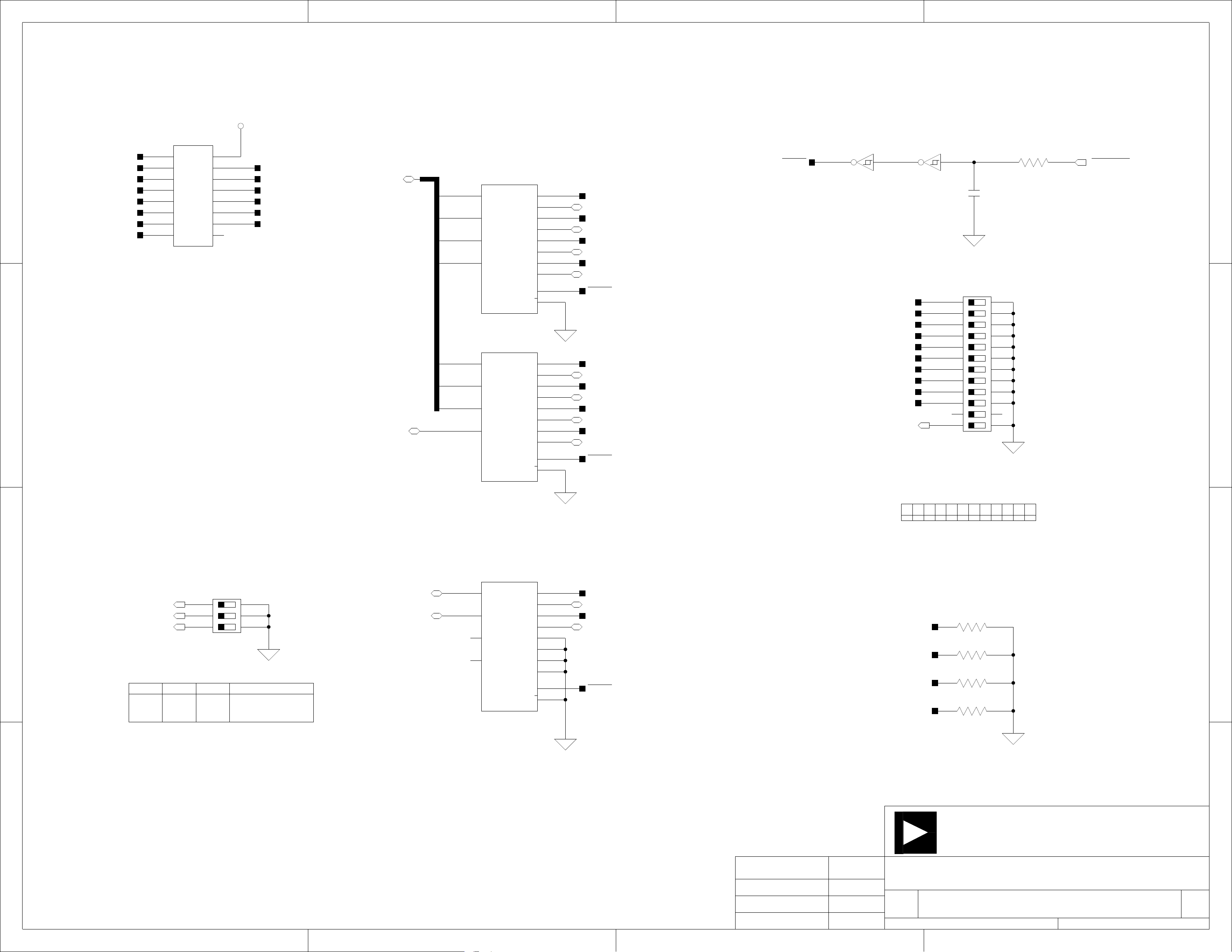
A B C D
3.3V
1
BMODE0
BMODE1
BMODE2
MS0
MS1
MS2
MS3
MS4
2
RN5
1
R1
3
R3
4
R4
5
R5
6
R6
7
R7
8 9
R8 R9
10K
RNET16
COM
R15R2
R14
R13
R12
R11
R10
DF
U9
74LVC14A
SOIC14
56
C19
0.01UF
805
SW2
1 2 4 5 6 7
3 8 9 10 11 12
SWT014
DIP12
ON
24
23
22
21
20
19
18
17
16
15
14
13
1
2
3
4
5
6
7
8
9
10
11
12
16
152
14
13
12
11
10
MS5
MS6
DF
SSEL0
SSEL1
BYPASS
MS_PF[0:6]
DF_PF7
MS_PF0
MS_PF1
MS_PF2
MS_PF3
MS_PF4
MS_PF5
MS_PF6
U20
4
YA
7
YB
9
YC
12
YD
ADG774A
QSOP16
U21
4
YA
7
YB
9
YC
12
YD
I0A
I1A
I0B
I1B
I0C
I1C
I0D
I1D
I0A
I1A
I0B
I1B
I0C
I1C
I0D
I1D
2
3
5
6
11
10
14
13
1
S
15
E
2
3
5
6
11
10
14
13
MS0
PF0
MS1
PF1
MS2
PF2
MS3
PF3
MUL_SEL
MS4
PF4
MS5
PF5
MS6
PF6
DF
PF7
U9
74LVC14A
SOIC14
98
MS0
MS1
MS2
MS3
MS4
MS5
MS6
SSEL0
SSEL1
BYPASS
R65
16K
1206
1
DSP_RESET_1MUL_SEL
2
1
S
15
E
QS3257Q
QSOP16
U22
4
SW1
3
BMODE0
BMODE1
BMODE2
SW1 SETTINGS: BOOT MODE SELECTION
ON
ON
*
ON
ON
OFF
* = DEFAULT
ON
ON
OFF
OFF
1
2
3
BMODE0BMODE1BMODE2 BOOT MODE
ON
OFF
ON
OFF
ON
1 2
3
SWT015
DIP3
-- ALL OTHERS RESERVED
6
5
4
EXECUTE 16-BIT EXTERNAL
8-BITS ROM
SPI0 ROM (8-BIT ADDRESS)
SPI0 ROM (16-BIT ADDRESS)
SSEL0_PF8
SSEL1_PF9
YA
7
YB
9
YC
12
YD
QS3257Q
QSOP16
I0A
I1A
I0B
I1B
I0C
I1C
I0D
I1D
2
3
5
6
11
10
14
13
1
S
15
E
MUL_SEL
SSEL0
PF8
SSEL1
PF9
MUL_SEL
SW2: CLOCK MULTIPLIER SELECT SWITCH
1 32 4ON5ON6ON7
OFFOFF ONONON
OFFOFF
DEFAULT SETTINGS:
Internal Clock - 15:1 - 300MHZ
External Clock - 2.5:1 - 120MHZ
REFER TO DSP HARDWARE REFERENCE FOR
DETAILED SETTING INFOMATION
PF0
PF1
PF2
PF3
8 9 10 11 12
ON
R66
10K
805
R120
10K
805
R121
10K
805
R122
10K
805
OFF
3
ANALOG
20 Cotton Road
Nashua, NH 03063
4
Approvals Date
Title
DEVICES
PH: 1-800-ANALOGD
4
ADSP-BF535 EZ-KIT LITE - CONFIG
Drawn
Checked
Engineering
Size Board No.
C
A0162-2000
Date Sheet of
A B C D
Rev
1.6
1253-12-2003_15:48
Page 68

A B C D
3.3V
R83
10K
805
PF4
1
SW4
SWT013
SPST-MOMENTARY
R82
100
805
CT9
1UF
A
U10
74LVC14A
SOIC14
89
R63
0.00
1206
PF4
3.3V
1
3.3V
R90
3.3V
3.3V
USB_CONFIGURED
R84
10K
805
PF5
SW5
SWT013
SPST-MOMENTARY
2
R85
100
805
CT10
1UF
A
U10
5 6
74LVC14A
SOIC14
R64
0.00
1206
PF5
SW8
SWT013
SPST-MOMENTARY
SOFT_RESET
R68
10K
805
U23
4
PFI
ADM708SAR
SOIC8
RESETMR
RESET
PFO
81
7
5
10K
805
RESET
9
10
74LVC00AD
SOIC14
U13
8
U24
2
1A1
4
1A2
6
1A3
8
1A4
PF[0:3]
PF0
PF1
PF2
PF3
11
2A1
13
2A2
15
2A3
17
2A4
1
OE1
19
OE2
IDT74FCT3244APY
SSOP20
USB_RESET
18
1Y1
16
1Y2
14
1Y3
12
1Y4
9
2Y1
7
2Y2
5
2Y3
3
2Y4
DSP_RESET_1
PF3 PF2 PF1 PF0
AMBER-SMT
LED001
LED2LED3
AMBER-SMT
LED001
LED7
RED-SMT
LED001
R76 R75
270
1206
LED1
AMBER-SMT
LED001
RESETUSB RESET
LED8
RED-SMT
LED001
270
1206
LED4
AMBER-SMT
LED001
5V
POWER
LED6
GREEN-SMT
LED001
2
3.3V
R72R71
1206
3.3V
U10
21
U13
4
5
74LVC00AD
SOIC14
R70R69
1206
6
270
1206
R88
10K
805
PF6
SW6
SWT013
3
SPST-MOMENTARY
R89
100
805
3.3V
CT12
1UF
A
U10
74LVC14A
SOIC14
R115
0.00
1011
1206
PF6
3.3V
U13
1
2
74LVC00AD
SOIC14
U9
74LVC14A
SOIC14
U9
74LVC14A
SOIC14
3
3.3V
21
R78
10K
805
1213
R79
10K
805
270270
1206
R80
10K
805
74LVC14A
SOIC14
R74
680270
1206
R81
10K
805
U10
3 4
74LVC14A
SOIC14
3
R91
R87
10K
805
PF7
SW7
SWT013
SPST-MOMENTARY
4
R86
100
805
13 12
CT11
1UF
A
U10
74LVC14A
SOIC14
R116
0.00
1206
PF7
NMI
SW3
SWT013
SPST-MOMENTARY
R67
100
805
10K
805
11 10
CT13
1UF
A
U9
74LVC14A
SOIC14
R117
0.00
1206
NMI
Approvals Date
Title
ANALOG
DEVICES
20 Cotton Road
Nashua, NH 03063
PH: 1-800-ANALOGD
4
ADSP-BF535 EZ-KIT LITE - RESET/PB/LED
Drawn
Checked
Engineering
Size Board No.
C
A0162-2000
Date Sheet of
A B C D
Rev
1.6
1263-13-2003_19:50
Page 69

D[0:31]
A B C D
A[2:25]
1
5V
3.3V
1.5V
3.3V
1
DSP JTAG HEADER
P2
CON017
45X2
1
3
5
78
9
1112
1314
1516
1718
19
2122
2324
2526
2728
29
3132
3334
3536
3738
39
4142
4344
4546
4748
49
51
53
55
57
59
61
63
65
67
69
71
73
75
77
79
81
83
85
87
SWE
SA10
~ABE0/SDQM0
~ABE1/SDQM1
~ABE2/SDQM2
~ABE3/SDQM3
AWE
ARE
AOE
~ABE0/SDQM0
~ABE1/SDQM1
~ABE2/SDQM2
~ABE3/SDQM3
PF0
PF6
TCLK1
TFS1
DT1
SCK1
MOSI1
MISO1
RX1
TX1
TMR2
PA0
PA1
PA2
PA3
PA4
PA5
PA6
PA7
RESET
RESET
P1
CON017
45X2
1
3
5
78
9
1112
1314
1516
1718
19
2122
2324
2526
2728
29
3132
3334
3536
3738
39
4142
4344
4546
4748
49
51
53
55
57
59
61
63
65
67
69
71
73
75
77
79
81
83
85
87
A2
A4
A6
A8
A10
A12
A14
A16
A18
A20
A22
D0
D2
D4
D6
D8
D10
D12
D14
D16
D18
D20
D22
D24
D26
D28
~ABE0/SDQM0~ABE3/SDQM3
SCLK0
SCAS
SRAS
SCKE
SMS0
SMS1
SMS2
SMS3
ARDY
AMS0
AMS1
AMS2
AMS3
PF1
PF3 PF2
PF5 PF4
PF7
PF9 PF8
PF11 PF10
PF13 PF12
PF15 PF14
RCLK1
RFS1
DR1
SCK0
MOSI0
MISO0
RX0
TX0
TMR1 TMR0
NMI
2
4
6
A3
A5
A7
A9
A11
A13
A15
A17
A19
A21
A23
A25 A24
10
20
30
2
D1
D3
D5
D7
D9
D11
D13
D15
D17
D19
D21
D23
D25
D27
D29
D31 D30
3
40
50
52
54
56
58
60
62
64
66
68
70
72
74
76
78
80
82
84
86
88
90 89
2
4
6
10
20
30
40
50
52
54
56
58
60
62
64
66
68
70
72
74
76
78
80
82
84
86
88
90 89
P3
CON017
45X2
1
3
5
78
9
1112
1314
1516
1718
19
2122
2324
2526
2728
29
3132
3334
3536
3738
39
4142
4344
4546
4748
49
51
53
55
57
59
61
63
65
67
69
71
73
75
77
79
81
83
85
87
2
4
6
10
20
30
40
50
52
54
56
58
60
62
64
66
68
70
72
74
76
78
80
82
84
86
88
90 89
USB_CLK
USB_XVER_DATA
USB_DPLS
USB_DMNS
USB_TXDLPLS
USB_TXDMNS
USB_TXEN
USB_SUSPEND
SLEEP
CLKOUT
DT0
TFS0
TCLK0
R57
10K
805
P8
1
3
5
7
9
11
13
IDC7X2
SPORT0
2
4
6
8
10
12
14
P9
1
3
5
7
9
11
13
15
17
19
CON014
10X2
HEADER_SELECT
HEADER_EMU
HEADER_TMS
HEADER_TCK
HEADER_TRST
HEADER_TDI
HEADER_TDO
2
4
6
8
10
12
14
16
18
20
2
RCLK0
3
RFS0
DR0
ANALOG
20 Cotton Road
Nashua, NH 03063
4
Approvals Date
Title
DEVICES
PH: 1-800-ANALOGD
4
ADSP-BF535 EZ-KIT LITE - CONNECTORS
Drawn
Checked
Engineering
Size Board No.
C
A0162-2000
Date Sheet of
A B C D
Rev
1.6
1273-13-2003_19:50
Page 70

A B C D
1
1 1 1
1 1 0
1 0 1
1 0 0
0 1 1
10
0
00
* = DEFAULT
WAIT 100uS FOR VOLTAGE TO SETTLE
AFTER CHANGING PF11-9
UNREG_IN
L1
10UH
IND001
VR5
1
2
IN1
2
IN2
SW
DRV
8
7
PWR_MGT_OUT
R95
53.6K
805
C21
470PF
1206
0
10
0
VDD_INTPF14 PF13 PF12
1.6V
1.5V *
1.4V
1.3V
1.2V
1.1V
1.0V
0.9V
3V_DSP
1
2
3
GND1 GND2
4
C22
1UF
805
C20
470PF
1206
3
R104
20.0K
1206
COMP
ADP3088
MSOP8
R96
DNP
1206
C23
DNP
805
FB
6
5
D4
1A
DO-214AA
R97
0.00
1206
R98
DNP
1206
M3
BSS123
SOT23D
3
2
R100
665K
805
1
M2
SOT23D
3
2
R101
332K
805
1BSS123
M1
BSS123
SOT23D
3
2
R102
165K
805
1
R99
DNP
1206
R103
316K
805
10K
805
R93R92
10K
805
R94
DNP
805
PF14
PF13
PF12
3
DNP
805
R124R123
DNP
805
ANALOG
R125
10K
805
20 Cotton Road
Nashua, NH 03063
4
DEVICES
PH: 1-800-ANALOGD
4
Approvals Date
Title
ADSP-BF535 EZ-KIT LITE - POWER 1
Drawn
Checked
Engineering
A B C D
Size Board No.
C
A0162-2000
Date Sheet of
Rev
1.6
1283-12-2003_15:48
Page 71

A B C D
1
5V
P10
1
7.5V_POWER
CON005
3
2
C25
1000PF
1206
C26
1000PF
1206
F1
2.5A
FUS001
D3
2A
DO-214AA
FER9
CHOKE_COIL
FER002
4
1
D2
2A
3
2
DO-214AA
R109
100K
1206
UNREG_IN
CT16
10UF
C
C27
0.1UF
805
VR4
3
INPUT OUTPUT
GND
1
ADP3339AKC-5
SOT-223
2
CT17
10UF
C
R110
0.00
RC05
C28
0.1UF
805
5V
FER6
600
1206
A5V
1
2
SHGND
5V
VR2
3
INPUT OUTPUT
5V
GND
1
2
ADP3338AKC-33
SOT-223
CT18
10UF
C
R113
0.00
1206
3V_DSP
C29
805
VDD_INT
D1
2A
DO-214AA
5V
VR1
3
INPUT OUTPUT
GND
1
ADP3338AKC-33
SOT-223
3.3V
R111
0.00
CT15
10UF
C
1206
C24
0.1UF0.1UF
805
2
FER7
600
1206
FER8
600
1206
SHGND
2
3
MH5MH4MH1 MH3MH2
R105
10K
805
VR3
2
INPUT
6 1
SD
OUTPUT
GND
4
ADP3331ART
SOT23-6
ERR
FB
1.5V
R126
3
5
R106
243.0K
R128
34.8K
805
805
R108
1.00M
1210
CT14
0.47UF
A
0.00
1206
CT1
22UF
D
ANALOG
SHGND
20 Cotton Road
3
Nashua, NH 03063
4
DEVICES
PH: 1-800-ANALOGD
4
Approvals Date
Title
ADSP-BF535 EZ-KIT LITE - POWER 2
Drawn
Checked
Engineering
A B C D
Size Board No.
C
Date Sheet of
3-25-2003_9:02 9 12
A0162-2000
Rev
1.6
Page 72

A B C D
3.3V
3.3V 3.3V
1
C48
805
C93
10UF
1210
C47
0.01UF
805 805
C95
10UF
1210
C44
0.01UF0.01UF
MT48LC4M16 (U5) MT48LC4M16 (U6)
C98
10UF
1210
C45
0.01UF
805
C82
0.01UF
805
C81
805
C46
805805
C50
0.01UF
C78
0.01UF0.01UF
C49
0.01UF 0.01UF
805
C79
0.01UF
805805
C80
805
C54
0.01UF 0.01UF
805
C83
805
C55
0.01UF
C84
0.01UF0.01UF
C53
805 805
C85
805805
C52
0.01UF
C86
0.01UF0.01UF
C51
0.01UF
805
C87
0.01UF
805805
C56
0.01UF
805805
C77
0.01UF0.01UF
C57
805
C76
805805
C102
0.01UF
805
C75
0.01UF0.01UF
805
C43
0.01UF
805
PSD4135 (U4)
C71
805
VDD_EXTVDD_INT
C69
0.01UF0.01UF
805
C42
0.01UF0.01UF
805
C70
0.01UF 0.01UF
805
C68
805 805
C72
0.01UF 0.01UF
C73
805 805
C74
0.01UF
C63
0.01UF
805
1
VDD_RTCVDD_PLL
C64
0.01UF
805
2
CT21
10UF
B
C107
0.01UF 0.01UF
805
C106
805
C38
0.01UF 0.01UF
C32
805
CYC64603-128 (U11)
ADSP-21535 INTERNAL (U1)
C39
805805
C97
0.01UF0.01UF
C103
805805
C104
0.01UF0.01UF
C105
0.01UF
805805
C61
0.01UF
805 805
C58
0.01UF
QS3257 (U14, U15, U20, U21, U22) ADSP-21535 PCI (U1) IDT74FCT3244APY (U24)
3.3V
C59
0.01UF
805 805
C60
0.01UF
805
C62
0.01UF
ADSP-21535 EXTERNAL (U1)
C88
0.01UF
C89
805805
VDD_PCIEXT
C91
0.01UF
C90
0.01UF0.01UF
805
C92
0.01UF
805805
ADSP-21535 PLL (U1) ADSP-21535 RTC (U1)
3.3V3.3V 3.3V
C36
0.01UF
805
C37
0.01UF
805
C108
0.01UF
805
74LVC14A (U9, U10, U19)
C34
0.01UF
805
C35
0.01UF
805
2
3
3.3V
CT19
10UF
B
AD1885JST DIGITAL (U7) AD1885JST ANALOG (U7)
C40
0.01UF
805
C41
0.01UF
805
CT20
10UF
B
C65
805
A5V
AGND
C66
0.01UF
805
C67
0.01UF0.01UF
805
3.3V3.3V
C96
C31
0.01UF
805
CY7C1019V33-15VC (U12) ADP3088 (VR5)CY7C4201V-15AC (U18)
C30
0.01UF
805
SN74LV164A (U17)
0.01UF
C109
0.01UF
805
SN74AHC1G00 (U26)SN74AHC1G02 (U16)
C116
0.01UF
805
C94
0.01UF
805805
C100
805
ADM708SAR (U23)
ANALOG
C101
0.01UF
805
20 Cotton Road
3.3V3.3V3.3V 3.3V3.3V 3.3V3.3V
C99
0.01UF0.01UF
805
24LC00-SN (U25) 74LVC00AD (U13)
C33
0.01UF
805
3
Nashua, NH 03063
4
DEVICES
PH: 1-800-ANALOGD
4
Approvals Date
Title
ADSP-BF535 EZ-KIT LITE - BYPASS CAPS
Drawn
Checked
Engineering
A B C D
Size Board No.
C
A0162-2000
Date Sheet of
Rev
1.6
12103-12-2003_15:48
Page 73

A B C D
1
1
All USB interface circuitry is considered proprietary
and has been omitted from this schematic
2
2
When designing your JTAG interface please refer to
the Engineer to Engineer Note EE-68 which can be found at
http://www.analog.com
3
ANALOG
4
DEVICES
20 Cotton Road
Nashua, NH 03063
PH: 1-800-ANALOGD
3
4
Approvals Date
Title
ADSP-BF535 EZ-KIT LITE - USB INTERFACE
Drawn
Checked
Engineering
A B C D
Size Board No.
C
Date Sheet of
A0162-2000
Rev
1.6
12113-25-2003_11:11
Page 74

IINDEX
A
AD1885 audio codecs, -xi, 1-11, 2-3, 2-5, 2-6
~AMS0 asynchronous memory select pin, 1-7,
2-3
architecture, of this EZ-KIT Lite, 2-2
ASYNC memory bank 0, 1-8
audio
codec disable jumper (JP2), 2-6
input jack (P5), 2-3, 2-5, 2-13
input select jumper (JP1), 2-5
interface, See SPORT0
output jack (P6), 2-3, 2-13
B
background telemetry channel (BTC), 1-13
bill of materials, A-1
BMODE2-0 (boot mode select) pins, 2-7
board schematic, B-1
boot
modes, 1-10
mode select switch (SW1), -xiii, 2-7
C
configuration, of this EZ-KIT Lite, 1-3
connectors
diagram of locations, 1-3, 2-12
P10 (power), 2-15
P1 (expansion), 2-3, 2-4, 2-12
P2 (expansion), 1-12, 2-3, 2-4, 2-12
P3 (expansion), -xiv, 2-3, 2-4, 2-12
P4 (FlashLINK devices), 2-13
P5 (audio in), 2-3, 2-5, 2-13
P6 (audio out), 2-3, 2-13
P7 (USB), 2-14
P8 (JTAG), 2-5, 2-14
P9 (SPORT0), 2-4, 2-15
contents, of this EZ-KIT Lite package, 1-2
core
clocks, 2-7
voltage, 1-12, 2-2
customer support, -xvii
D
default configuration, of this EZ-KIT Lite, 1-3,
1-8
DF pin, 2-7
DF signal, 2-8
E
EBIU_SDBCTL register, 1-9
EBIU_SDGCTL register, 1-9
EBIU_SDRRC register, 1-9
EBUI control signals, 2-4
example programs, 1-13
expansion interface, 2-3, 2-4, 2-12, 2-17
ADSP-BF535 EZ-KIT Lite Evaluation System Manual I-1
Page 75

INDEX
external bus interface unit, See EBIU
external memory, 2-16
See also flash memory
address map, 1-8
connections, 2-5
power supply, 2-16
F
features, of this EZ-KIT Lite, -xi
FIO_DIR register, 1-12
FIO_FLAG_S/C registers, 1-12
flags, See programmable flags (PFs)
FlashLINK devices, 1-9, 2-13
flash memory
connections, 2-3
devices, 1-9
FlashLINK connector (P4), 2-13
memory map, 1-7
programming/configuring, 1-9
frequency, 1-12
G
general-purpose IO pins, 1-11, 2-7, 2-11
H
Help, online, -xxvi
I
input clock, 2-2, 2-7
installation, of this EZ-KIT Lite, 1-5
interfaces, See expansion, SPORT0, EBIU, PCI
internal memory
core MMRs, 1-8
data banks A, B, 1-8
instruction SRAM, 1-8
L2 SRAM, 1-7, 1-8
reserved, 1-8
scratch pad, 1-8
system MMRs, 1-8
via JTAG, 2-5
J
JTAG
connector (P8), 2-5, 2-14
emulation port, 2-5
jumpers
settings, 1-3, 2-5
JP1 (audio input select), 2-3, 2-5
JP2 (AD1885 disable), 2-4, 2-6
L
LEDs
diagram of locations, 1-3, 2-9
LED1-4 (PF3-0), 1-11
LED5 (USB monitor), 1-5, 2-10
LED6 (power), 2-10
LED7 (USB reset), 2-10
LED8 (processor reset), 2-10
LINE_IN stereo input channel, 2-3, 2-5
M
measurements, of this EZ-KIT Lite, 2-16
mechanical dimensions, of this EZ-KIT Lite,
2-17
memory
map, of this EZ-KIT Lite, 1-7
select pins, See ~AMS0, ~SMS0
memory mapped register (MMR), 1-12
MIC1 mono input channel, 2-3, 2-5
I-2 ADSP-BF535 EZ-KIT Lite Evaluation System Manual
Page 76

INDEX
MSEL6-0 pins, 2-7, 2-8
N
NMI (non-maskable interrupt) push button
(SW3), 2-11
notation conventions, -xxviii
P
package contents, of this EZ-KIT Lite, 1-2
PCI interface, 2-16
peripheral interface
connectors, -xiv, 2-12
speed, 2-8
voltage, 2-2
phase lock loop, See PLL
PLL
power supply, 2-16
setup signals, 2-7, 2-8
setup switch (SW2), 2-2, 2-7
PMGMT2-0 pins, 1-11
power
connector (P10), 2-15
LED (LED6), 2-10
management, 1-11, 1-12
specifications, 2-15
supplies, 2-16
programmable flags (PFs)
PF0-3 (LED1-4), 1-11, 2-9, 2-10
PF12-14 (core voltage), 1-11, 1-12
PF15 (AD1885 reset), 1-11, 2-4, 2-6
PF4-7 (SW4-7), 1-11, 2-11
PF8-11 (general-purpose IO), 1-11
push buttons
See also switches by name (SWx)
diagram of locations, 2-9
R
RCLK0 pin, 2-4
real-time clock (RTC), 2-3, 2-16
registration, of this product, 1-3
regulatory compliance, -iii
reset
AD1885 codec, 2-4, 2-6
LEDs (LED7-8), 2-10
processor, 1-11, 2-2, 2-7
push button (SW8), 2-11
restrictions, of the license, 1-7
RTC pin, 2-3
S
schematic, of this EZ-KIT Lite, B-1
SDRAM
connections, 1-7, 2-3
control registers, 1-8
default settings, 1-9
memory map, 1-8
setup, of this EZ-KIT Lite, 1-3
~SMS0 synchronous memory select pin, 1-7,
2-3
specifications, of this EZ-KIT Lite, 2-15
SPORT0
audio interface, -xiii, 2-3
connector (P9), 2-15
SSEL1-0 pins, 2-7, 2-8
startup, of this EZ-KIT Lite, 1-5
stereo input channels, 2-3, 2-5
SW1 (boot mode select) switch, 2-7
SW2 (PLL setup) switch, 2-2, 2-7
SW3 (NMI) push button, 2-11
SW4-7 (general-purpose IO) push buttons,
1-11, 2-11
SW8 (reset) push button, 2-11
switches
See also switches by name (SWx)
diagram of locations, 1-3
synchronous dynamic random access memory,
See SDRAM
ADSP-BF535 EZ-KIT Lite Evaluation System Manual I-3
Page 77

INDEX
system architecture, of the EZ-KIT Lite board,
2-2
T
Target Options dialog box, 1-8
TCLK0 pin, 2-4
U
USB
cable, 1-3
connector (P7), 2-14
interface, 2-5, 2-11
monitor LED (LED5), 1-5, 2-10
port, -xiv
reset LED (LED7), 2-10
V
VDD_INT signal, 1-12
VisualDSP++
documentation, -xxvii
environment, 1-5
online Help, -xxvi
voltage regulators, -xiii, 2-16
I-4 ADSP-BF535 EZ-KIT Lite Evaluation System Manual
 Loading...