

Blackfin
®
Embedded Processor
Preliminary Technical Data
FEATURES
Up to 500 MHz High-Performance Blackfin Processor
Two 16-Bit MACs, Two 40-Bit ALUs, Four 8-Bit Video
ALUs, 40-Bit Shifter
RISC-Like Register and Instruction Model for Ease of
Programming and Compiler-Friendly Support
Advanced Debug, Trace, and Performance-Monitoring
0.8V to 1.2V Core V
2.5 V and 3.3 V-Tolerant I/O with Specific 5 V-Tolerant Pins
182-Ball MBGA and 208-Ball Sparse MBGA Packages
Lead Bearing and Lead Free Package Choices
MEMORY
132K Bytes of On-Chip Memory:
16K Bytes of Instruction SRAM/Cache
48K Bytes of Instruction SRAM
32K Bytes of Data SRAM/Cache
32K Bytes of Data SRAM
4K Bytes of Scratchpad SRAM
External Memory Controller with Glueless Support for
SDRAM and Asynchronous 8/16-Bit Memories
Flexible Booting Options from External Flash, SPI and TWI
Memory or from SPI, TWI, and UART Host Devices
with On-chip Voltage Regulation
DD
ADSP-BF534
Two Dual-Channel Memory DMA Controllers
Memory Management Unit Providing Memory Protection
PERIPHERALS
Controller Area Network (CAN) 2.0B Interface
Parallel Peripheral Interface (PPI), Supporting ITU-R 656
Video Data Formats
Two Dual-Channel, Full-Duplex Synchronous Serial Ports
(SPORTs), Supporting Eight Stereo I
12 Peripheral DMAs
Two Memory-to-Memory DMAs With External Request Lines
Event Handler With 32 Interrupt Inputs
Serial Peripheral Interface (SPI)-Compatible
Two UARTs with IrDA® Support
Two-Wire Interface (TWI) Controller
Eight 32-Bit Timer/Counters with PWM Support
Real-Time Clock (RTC) and Watchdog Timer
32-Bit Core Timer
48 General-Purpose I/Os (GPIOs), 8 with High Current Drivers
On-Chip PLL Capable of 1x to 63x Frequency Multiplication
Debug/JTAG Interface
2
S Channels
JTAG TEST AND
EMULATION
VOLTAGE
REGULATOR
INSTRUCTION
MEMORY
CORE / SYSTEM BUS INTERFACE
Blackfin and the Blackfin logo are registered trademarks of Analog Devices, Inc.
Rev. PrD
Information furnished by Analog Devices is believed to be accurate and reliable.
However, no responsibility is assumed by Analog Devices for its use, nor for any
infringements of patents or other rights of third parties that may result from its use.
Specifications subject to change without notice. No license is granted by implication
or otherwise under any patent or patent rights of Analog Devices. Trademarks and
registered trademarks are the property of their respective owners.
EVENT
CONTROLLER/
CORE TIMER
B
L1
MMU
CONTROLLER
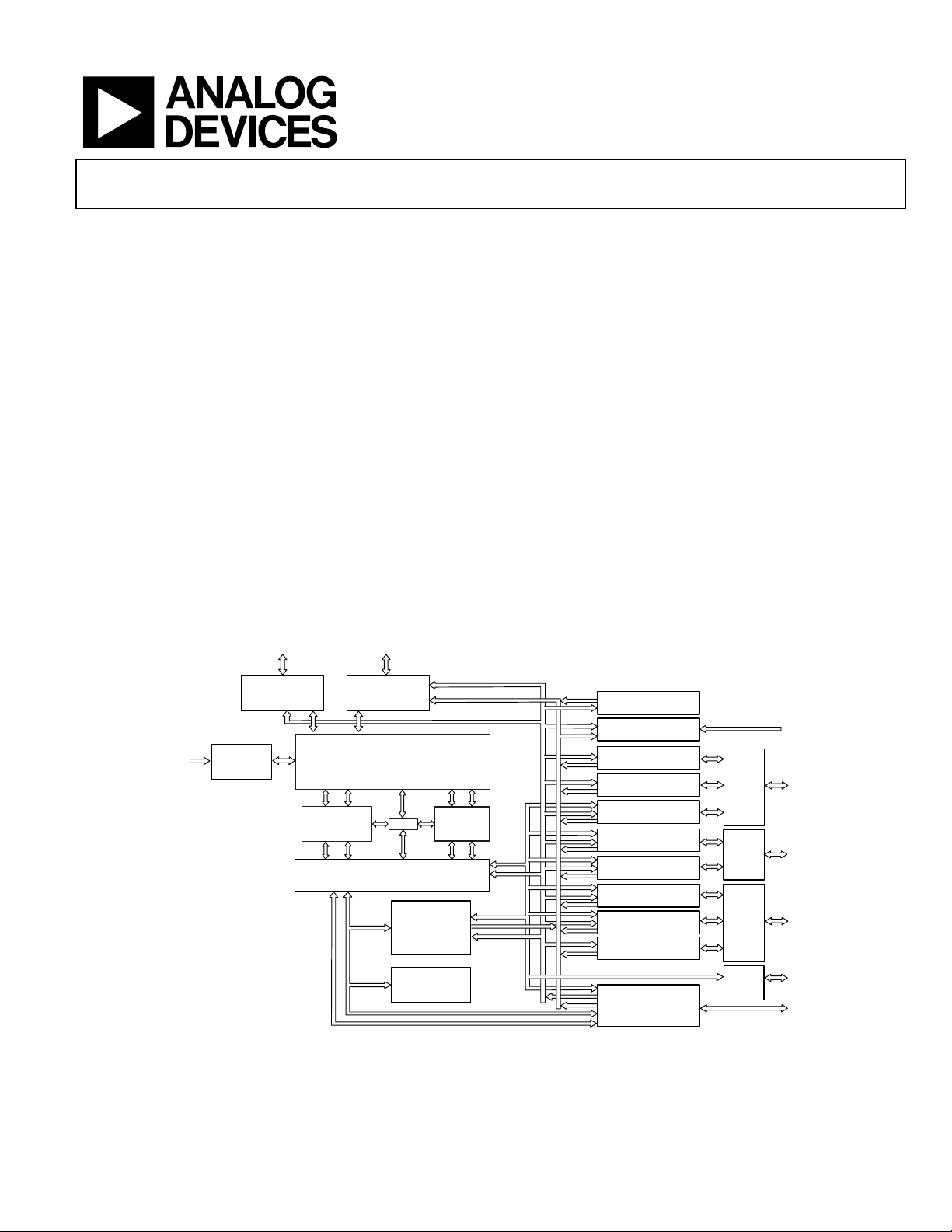
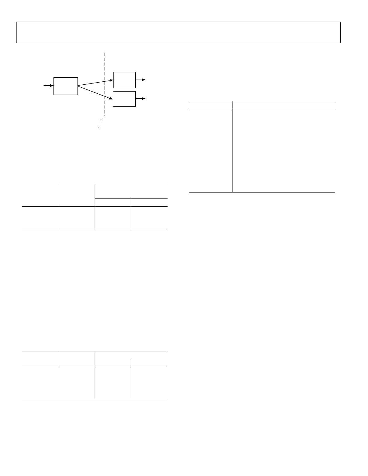
Figure 1. Functional Block Diagram
MEMORY
DMA
BOOT ROM
DATA
WATCHDOG TIMER
RTC
CAN
TWI
L1
One Technology Way, P.O.Box 9106, Norwood, MA 02062-9106 U.S.A.
Tel:781/329-4700 www.analog.com
Fax:781/326-8703 © 2005 Analog Devices, Inc. All rights reserved.
SPORT0
SPORT1
PPI
UART 0-1
SPI
TIMERS 0-7
EXTERNAL PORT
FLASH, SDRAM
CONTROL
PORT
J
GPIO
PORT
G
GPIO
PORT
F
GPIO
PORT
H

ADSP-BF534 Preliminary Technical Data
TABLE OF CONTENTS
General Description ................................................. 3
Portable Low-Power Architecture ............................. 3
System Integration ................................................ 3
ADSP-BF534 Processor Peripherals ... ........................ 3
Blackfin Processor Core .......................................... 4
Memory Architecture ............................................ 4
Internal (On-chip) Memory ................................. 4
External (Off-Chip) Memory ................................ 5
I/O Memory Space ............................................. 5
Booting ........................................................... 5
Event Handling ................................................. 5
Core Event Controller (CEC) ................................ 6
System Interrupt Controller (SIC) .......................... 6
Event Control ................................................... 6
DMA Controllers .................................................. 8
Real-Time Clock (RTC) .......................................... 8
Watchdog Timer .................................................. 9
Timers ............................................................... 9
Serial Ports (SPORTs) ............................................ 9
Serial Peripheral Interface (SPI) Port ......................... 9
UART Ports (UARTs) .......................................... 10
Controller Area Network (CAN) ............................ 10
TWI Controller Interface ...................................... 10
Ports ................................................................ 11
General-Purpose I/O (GPIO) .............................. 11
Parallel Peripheral Interface (PPI) ........................... 11
Dynamic Power Management ................................ 11
Full-On Operating Mode – Maximum Performance . 12
Active Operating Mode – Moderate Power Savings .. 12
Sleep Operating Mode – High Dynamic Power
Savings ....................................................... 12
Deep Sleep Operating Mode – Maximum Dynamic
Power Savings .............................................. 12
Hibernate Operating Mode – Maximum Static Power
Savings ....................................................... 12
Power Savings ................................................. 12
Voltage Regulation .............................................. 13
Clock Signals ..................................................... 13
Booting Modes ................................................... 14
Instruction Set Description ................................... 15
Development Tools ............................................. 15
Designing an Emulator-Compatible Processor
Board(Target) ................................................. 15
Related Documents .............................................. 16
Pin Descriptions .................................................... 17
Specifications ........................................................ 20
Recommended Operating Conditions ...................... 20
Absolute Maximum Ratings ................................... 22
ESD Sensitivity ................................................... 22
Timing Specifications ........................................... 23
Asynchronous Memory Read Cycle Timing ............ 25
Asynchronous Memory Write Cycle Timing ........... 26
SDRAM Interface Timing .................................. 27
External Port Bus Request and Grant Cycle Timing . . 28
External DMA Request Timing ............................ 29
Parallel Peripheral Interface Timing ...................... 30
Serial Ports ..................................................... 31
Serial Peripheral Interface (SPI) Port—Master
Timing ....................................................... 36
Serial Peripheral Interface (SPI) Port—Slave Timing . 37
Universal Asynchronous Receiver-Transmitter
(UART) Ports—Receive and Transmit Timing ..... 38
General-Purpose Port Timing ............................. 39
Timer Cycle Timing .......................................... 40
JTAG Test And Emulation Port Timing ................. 41
TWI Controller Timing ..................................... 42
Output Drive Currents ......................................... 46
Test Conditions .................................................. 49
Output Enable Time ......................................... 49
Output Disable Time ......................................... 50
Example System Hold Time Calculation ................ 50
Environmental Conditions .................................... 51
182-Ball Mini-BGA Pinout ....................................... 52
208-Ball Sparse Mini-BGA Pinout .............................. 55
Outline Dimensions ................................................ 58
Ordering Guide ..................................................... 60
Rev. PrD | Page 2 of 60 | January 2005

REVISION HISTORY
Revision PrD: Corrections to PrC because of changes to Ordering Guide, addition of driver type to Table 9, other minor
corrections.
Changes to:
Features ................................................................. 1
Figure 5 ................................................................ 13
Booting Modes ....................................................... 14
Table 9 ................................................................. 17
GENERAL DESCRIPTION
ADSP-BF534Preliminary Technical Data
Absolute Maximum Ratings ...................................... 22
Figure 8 ............................................................... 22
Figure 13 .............................................................. 28
Output Drive Currents ............................................ 46
Table 44 title ......................................................... 55
Table 45 title ......................................................... 56
Figure 47 title .........................................................59
Ordering Guide ..................................................... 60
The ADSP-BF534 processor is a member of the Blackfin family
of products, incorporating the Analog Devices/Intel Micro Signal Architecture (MSA). Blackfin processors combine a dualMAC state-of-the-art signal processing engine, the advantages
of a clean, orthogonal RISC-like microprocessor instruction set,
and single-instruction, multiple-data (SIMD) multimedia capabilities into a single instruction-set architecture.
Specific performance and memory configuration is shown in
Table 1.
Table 1. Processor Comparison
ADSP-BF534
Maximum performance 500 MHz
Instruction SRAM/Cache 16K bytes
Instruction SRAM 48K bytes
Data SRAM/Cache 32K bytes
Data SRAM 32K bytes
Scratchpad 4K bytes
By integrating a rich set of industry-leading system peripherals
and memory, Blackfin processors are the platform of choice for
next-generation applications that require RISC-like programmability, multimedia support and leading-edge signal
processing in one integrated package.
PORTABLE LOW-POWER ARCHITECTURE
Blackfin processors provide world-class power management
and performance. Blackfin processors are designed in a low
power and low voltage design methodology and feature on-chip
Dynamic Power Management, the ability to vary both the voltage and frequency of operation to significantly lower overall
power consumption. Varying the voltage and frequency can
result in a substantial reduction in power consumption, compared with just varying the frequency of operation. This
translates into longer battery life for portable appliances.
SYSTEM INTEGRATION
The ADSP-BF534 processor is a highly integrated system-on-achip solutions for the next generation of embedded network
connected applications. By combining industry-standard interfaces with a high performance signal processing core, users can
develop cost-effective solutions quickly without the need for
costly external components. The system peripherals include a
CAN 2.0B controller, a TWI controller, two UART ports, an SPI
port, two serial ports (SPORTs), nine general purpose 32-bit
timers (eight with PWM capability), a real-time clock, a watchdog timer, and a Parallel Peripheral Interface.
ADSP-BF534 PROCESSOR PERIPHERALS
The ADSP-BF534 processor contains a rich set of peripherals
connected to the core via several high bandwidth buses, providing flexibility in system configuration as well as excellent overall
system performance (see the block diagram on page 1). The
general-purpose peripherals include functions such as UARTs,
SPI, TWI, Timers with PWM (Pulse Width Modulation) and
pulse measurement capability, general purpose I/O pins, a RealTime Clock, and a Watchdog Timer. This set of functions satisfies a wide variety of typical system support needs and is
augmented by the system expansion capabilities of the part. The
ADSP-BF534 processor contains dedicated network communication modules and high-speed serial and parallel ports, an
interrupt controller for flexible management of interrupts from
the on-chip peripherals or external sources, and power management control functions to tailor the performance and power
characteristics of the processor and system to many application
scenarios.
All of the peripherals, except for general-purpose I/O, CAN,
TWI, Real-Time Clock, and timers, are supported by a flexible
DMA structure. There are also separate memory DMA channels
dedicated to data transfers between the processor's various
memory spaces, including external SDRAM and asynchronous
memory. Multiple on-chip buses running at up to 133 MHz
provide enough bandwidth to keep the processor core running
along with activity on all of the on-chip and external
peripherals.
The ADSP-BF534 processor includes an on-chip voltage regulator in support of the ADSP-BF534 processor Dynamic Power
Management capability. The voltage regulator provides a range
of core voltage levels when supplied from a single 2.25 V to
3.6 V input. The voltage regulator can be bypassed at the user's
discretion.
Rev. PrD | Page 3 of 60 | January 2005

ADSP-BF534 Preliminary Technical Data
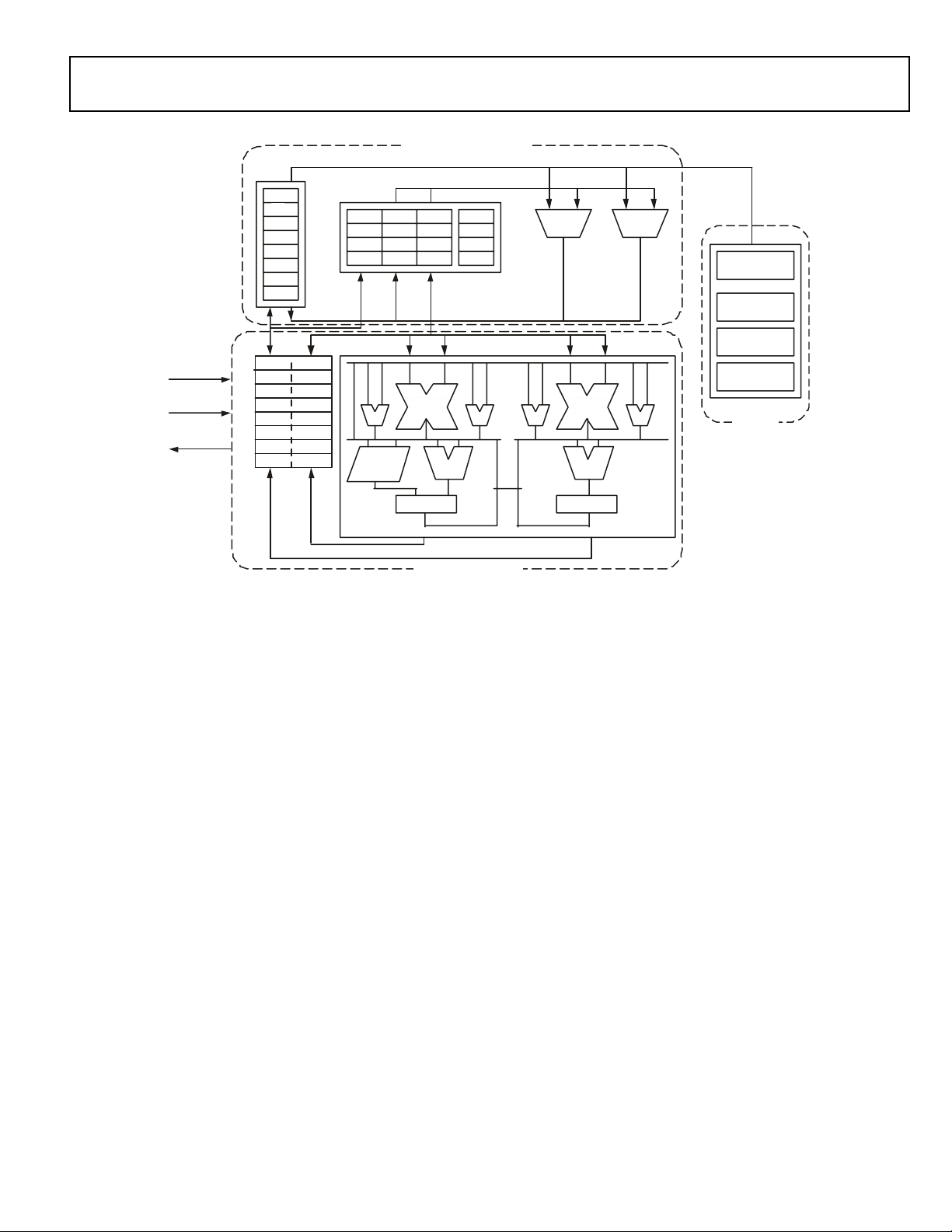
BLACKFIN PROCESSOR CORE
As shown in Figure 2 on page 5, the Blackfin processor core
contains two 16-bit multipliers, two 40-bit accumulators, two
40-bit ALUs, four video ALUs, and a 40-bit shifter. The computation units process 8-bit, 16-bit, or 32-bit data from the register
file.
The compute register file contains eight 32-bit registers. When
performing compute operations on 16-bit operand data, the
register file operates as 16 independent 16-bit registers. All
operands for compute operations come from the multiported
register file and instruction constant fields.
Each MAC can perform a 16-bit by 16-bit multiply in each
cycle, accumulating the results into the 40-bit accumulators.
Signed and unsigned formats, rounding, and saturation are
supported.
The ALUs perform a traditional set of arithmetic and logical
operations on 16-bit or 32-bit data. In addition, many special
instructions are included to accelerate various signal processing
tasks. These include bit operations such as field extract and population count, modulo 2
and rounding, and sign/exponent detection. The set of video
instructions include byte alignment and packing operations, 16bit and 8-bit adds with clipping, 8-bit average operations, and 8bit subtract/absolute value/accumulate (SAA) operations. Also
provided are the compare/select and vector search instructions.
For certain instructions, two 16-bit ALU operations can be performed simultaneously on register pairs (a 16-bit high half and
16-bit low half of a compute register). By also using the second
ALU, quad 16-bit operations are possible.
The 40-bit shifter can perform shifts and rotates and is used to
support normalization, field extract, and field deposit
instructions.
The program sequencer controls the flow of instruction execution, including instruction alignment and decoding. For
program flow control, the sequencer supports PC relative and
indirect conditional jumps (with static branch prediction), and
subroutine calls. Hardware is provided to support zero-overhead looping. The architecture is fully interlocked, meaning that
the programmer need not manage the pipeline when executing
instructions with data dependencies.
The address arithmetic unit provides two addresses for simultaneous dual fetches from memory. It contains a multiported
register file consisting of four sets of 32-bit Index, Modify,
Length, and Base registers (for circular buffering), and eight
additional 32-bit pointer registers (for C-style indexed stack
manipulation).
Blackfin processors support a modified Harvard architecture in
combination with a hierarchical memory structure. Level 1 (L1)
memories are those that typically operate at the full processor
speed with little or no latency. At the L1 level, the instruction
memory holds instructions only. The two data memories hold
data, and a dedicated scratchpad data memory stores stack and
local variable information.
32
multiply, divide primitives, saturation
In addition, multiple L1 memory blocks are provided, offering a
configurable mix of SRAM and cache. The Memory Management Unit (MMU) provides memory protection for individual
tasks that may be operating on the core and can protect system
registers from unintended access.
The architecture provides three modes of operation: User mode,
Supervisor mode, and Emulation mode. User mode has
restricted access to certain system resources, thus providing a
protected software environment, while Supervisor mode has
unrestricted access to the system and core resources.
The Blackfin processor instruction set has been optimized so
that 16-bit opcodes represent the most frequently used instructions, resulting in excellent compiled code density. Complex
DSP instructions are encoded into 32-bit opcodes, representing
fully featured multifunction instructions. Blackfin processors
support a limited multi-issue capability, where a 32-bit instruction can be issued in parallel with two 16-bit instructions,
allowing the programmer to use many of the core resources in a
single instruction cycle.
The Blackfin processor assembly language uses an algebraic syntax for ease of coding and readability. The architecture has been
optimized for use in conjunction with the C/C++ compiler,
resulting in fast and efficient software implementations.
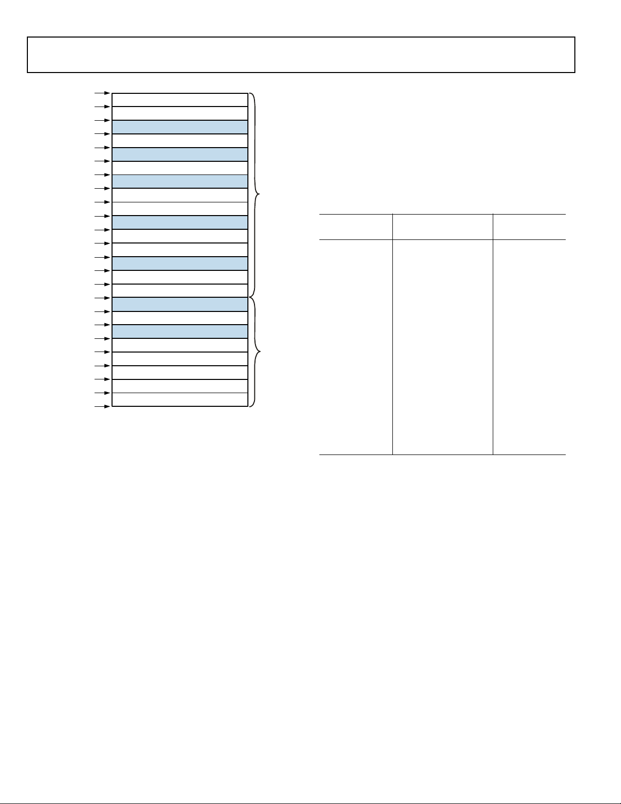
MEMORY ARCHITECTURE
The ADSP-BF534 processor views memory as a single unified
4G byte address space, using 32-bit addresses. All resources,
including internal memory, external memory, and I/O control
registers, occupy separate sections of this common address
space. The memory portions of this address space are arranged
in a hierarchical structure to provide a good cost/performance
balance of some very fast, low-latency on-chip memory as cache
or SRAM, and larger, lower-cost and performance off-chip
memory systems. See Figure 3 on page 6.
The on-chip L1 memory system is the highest-performance
memory available to the Blackfin processor. The off-chip memory system, accessed through the External Bus Interface Unit
(EBIU), provides expansion with SDRAM, flash memory, and
SRAM, optionally accessing up to 516M bytes of physical
memory.
The memory DMA controller provides high-bandwidth datamovement capability. It can perform block transfers of code or
data between the internal memory and the external memory
spaces.
Internal (On-chip) Memory
The ADSP-BF534 processor has three blocks of on-chip memory providing high-bandwidth access to the core.
The first block is the L1 instruction memory, consisting of
64K bytes SRAM, of which 16K bytes can be configured as a
four-way set-associative cache. This memory is accessed at full
processor speed.
The second on-chip memory block is the L1 data memory, consisting of two banks of 32K bytes each. Each memory bank is
configurable, offering both Cache and SRAM functionality. This
memory block is accessed at full processor speed.
Rev. PrD | Page 4 of 60 | January 2005
LD032BITS
LD132BITS
SD 3 2 BI TS
R7
R6
R5
R4
R3
R2
R1
R0
R7 .H
R6 .H
R5 .H
R4 .H
R3 .H
R2 .H
R1 .H
R0 .H
ADSP-BF534Preliminary Technical Data
ADDRE SS ARITHMETIC UNIT
SP
FP
P5
P4
P3
P2
P1
P0
R7.L
R6.L
R5.L
R4.L
R3.L
R2.L
R1.L
R0.L
I3
I2
I1
I0
BARREL
SHIF TER
L3
B3
L2
L1
L0
16
A0 A1
M3
B2
M2
B1
M1
B0
M0
88 8 8
40 40
DAG0 DA G 1
16
SEQUENCER
ALIGN
DECODE
LOOP BUF FER
CONTROL
UN IT
DATA ARITHMETIC UNI T
Figure 2. Blackfin Processor Core
The third memory block is a 4K byte scratchpad SRAM which
runs at the same speed as the L1 memories, but is only accessible
as data SRAM and cannot be configured as cache memory.
External (Off-Chip) Memory
External memory is accessed via the EBIU. This 16-bit interface
provides a glueless connection to a bank of synchronous DRAM
(SDRAM) as well as up to four banks of asynchronous memory
devices including flash, EPROM, ROM, SRAM, and memory
mapped I/O devices.
The PC133-compliant SDRAM controller can be programmed
to interface to up to 512M bytes of SDRAM. A separate row can
be open for each SDRAM internal bank and the SDRAM controller supports up to 4 internal SDRAM banks, improving
overall performance.
The asynchronous memory controller can be programmed to
control up to four banks of devices with very flexible timing
parameters for a wide variety of devices. Each bank occupies a
1M byte segment regardless of the size of the devices used, so
that these banks will only be contiguous if each is fully populated with 1M byte of memory.
I/O Memory Space
The ADSP-BF534 processor does not define a separate I/O
space. All resources are mapped through the flat 32-bit address
space. On-chip I/O devices have their control registers mapped
into memory-mapped registers (MMRs) at addresses near the
top of the 4G byte address space. These are separated into two
smaller blocks, one which contains the control MMRs for all
core functions, and the other which contains the registers
needed for setup and control of the on-chip peripherals outside
of the core. The MMRs are accessible only in supervisor mode
and appear as reserved space to on-chip peripherals.
Booting
The ADSP-BF534 processor contains a small on-chip boot kernel, which configures the appropriate peripheral for booting. If
the ADSP-BF534 processor is configured to boot from boot
ROM memory space, the processor starts executing from the
on-chip boot ROM. For more information, see Booting Modes
on page 14.
Event Handling
The event controller on the ADSP-BF534 processor handles all
asynchronous and synchronous events to the processor. The
ADSP-BF534 processor provides event handling that supports
both nesting and prioritization. Nesting allows multiple event
service routines to be active simultaneously. Prioritization
ensures that servicing of a higher-priority event takes precedence over servicing of a lower-priority event. The controller
provides support for five different types of events:
• Emulation – An emulation event causes the processor to
enter emulation mode, allowing command and control of
the processor via the JTAG interface.
• Reset – This event resets the processor.
Rev. PrD | Page 5 of 60 | January 2005
ADSP-BF534 Preliminary Technical Data
0xFFFF FFFF
0xFFE0 0000
0xFFC0 0000
0xFFB0 1000
0xFFB0 0000
0xFFA1 4000
0xFFA1 0000
0xFFA0 C000
0xFFA0 8000
0xFFA0 0000
0xFF90 8000
0xFF90 4000
0xFF90 0000
0xFF80 8000
0xFF80 4000
0xFF80 0000
0xEF00 0800
0xEF00 0000
0x2040 0000
0x2030 0000
0x2020 0000
0x2010 0000
0x2000 0000
0x0000 0000
CORE MMR REGISTERS (2M BYTE)
SYSTEM MMR RE GISTERS (2M BYTE)
RESERVED
SCRATCHPAD SRAM (4K BYTE)
RESERVED
INSTRUCTION SRAM / CACHE (16K BYTE)
RESERVED
INSTRUCTION BANK B SRAM (16K BYTE)
INSTRUCTION BANK A SRAM (32K BYTE)
RESERVED
DATA BANK B SRAM / CACHE (16K BYTE)
DATA BANK B SRAM (16K BYTE)
RESERVED
DATA BANK A SRAM / CACHE (16K BYTE)
DATA BANK A SRAM (16K BYTE)
RESERVED
BOOT ROM (2K BYTE)
RESERVED
ASYNC MEMORY BANK 3 (1M BYTE)
ASYNC MEMORY BANK 2 (1M BYTE)
ASYNC MEMORY BANK 1 (1M BYTE)
ASYNC MEMORY BANK 0 (1M BYTE)
SDRAM MEMORY (16M BYTE - 512M BYTE)
P
A
M
Y
R
O
M
E
M
L
A
N
R
E
T
N
I
P
A
M
Y
R
O
M
E
M
L
A
N
R
E
T
X
E
Figure 3. ADSP-BF534 Internal/External Memory Map
• Non-Maskable Interrupt (NMI) – The NMI event can be
generated by the software watchdog timer or by the NMI
input signal to the processor. The NMI event is frequently
used as a power-down indicator to initiate an orderly shutdown of the system.
• Exceptions – Events that occur synchronously to program
flow (i.e., the exception will be taken before the instruction
is allowed to complete). Conditions such as data alignment
violations and undefined instructions cause exceptions.
• Interrupts – Events that occur asynchronously to program
flow. They are caused by input pins, timers, and other
peripherals, as well as by an explicit software instruction.
Each event type has an associated register to hold the return
address and an associated return-from-event instruction. When
an event is triggered, the state of the processor is saved on the
supervisor stack.
The ADSP-BF534 processor Event Controller consists of two
stages, the Core Event Controller (CEC) and the System Interrupt Controller (SIC). The Core Event Controller works with
the System Interrupt Controller to prioritize and control all system events. Conceptually, interrupts from the peripherals enter
into the SIC, and are then routed directly into the general-purpose interrupts of the CEC.
Core Event Controller (CEC)
The CEC supports nine general-purpose interrupts (IVG15– 7),
in addition to the dedicated interrupt and exception events. Of
these general-purpose interrupts, the two lowest-priority interrupts (IVG15–14) are recommended to be reserved for software
interrupt handlers, leaving seven prioritized interrupt inputs to
support the peripherals of the ADSP-BF534 processor. Table 2
describes the inputs to the CEC, identifies their names in the
Event Vector Table (EVT), and lists their priorities.
Table 2. Core Event Controller (CEC)
Priority
Event Class EVT Entry
(0 is Highest)
0Emulation/Test ControlEMU
1 Reset RST
2 Non-Maskable Interrupt NMI
3ExceptionEVX
4 Reserved —
5 Hardware Error IVHW
6 Core Timer IVTMR
7 General Interrupt 7 IVG7
8 General Interrupt 8 IVG8
9 General Interrupt 9 IVG9
10 General Interrupt 10 IVG10
11 General Interrupt 11 IVG11
12 General Interrupt 12 IVG12
13 General Interrupt 13 IVG13
14 General Interrupt 14 IVG14
15 General Interrupt 15 IVG15
System Interrupt Controller (SIC)
The System Interrupt Controller provides the mapping and
routing of events from the many peripheral interrupt sources to
the prioritized general-purpose interrupt inputs of the CEC.
Although the ADSP-BF534 processor provides a default mapping, the user can alter the mappings and priorities of interrupt
events by writing the appropriate values into the Interrupt
Assignment Registers (IAR). Table 3 describes the inputs into
the SIC and the default mappings into the CEC.
Event Control
The ADSP-BF534 processor provides the user with a very flexible mechanism to control the processing of events. In the CEC,
three registers are used to coordinate and control events. Each
register is 16 bits wide:
• CEC Interrupt Latch Register (ILAT) – The ILAT register
indicates when events have been latched. The appropriate
bit is set when the processor has latched the event and
cleared when the event has been accepted into the system.
Rev. PrD | Page 6 of 60 | January 2005

ADSP-BF534Preliminary Technical Data
Table 3. System Interrupt Controller (SIC)
Peripheral Interrupt Event Default
Mapping
PLL Wakeup IVG7 0
DMA Error (generic) IVG7 1
DMAR0 Block Interrupt IVG7 1
DMAR1 Block Interrupt IVG7 1
DMAR0 Overflow Error IVG7 1
DMAR1 Overflow Error IVG7 1
CAN Error IVG7 2
SPORT 0 Error IVG7 2
SPORT 1 Error IVG7 2
PPI Error IVG7 2
SPI Error IVG7 2
UART0 Error IVG7 2
UART1 Error IVG7 2
Real-Time Clock IVG8 3
DMA Channel 0 (PPI) IVG8 4
DMA Channel 3 (SPORT 0 RX) IVG9 5
DMA Channel 4 (SPORT 0 TX) IVG9 6
DMA Channel 5 (SPORT 1 RX) IVG9 7
DMA Channel 6 (SPORT 1 TX) IVG9 8
TWI IVG10 9
DMA Channel 7 (SPI) IVG10 10
DMA Channel 8 (UART0 RX) IVG10 11
DMA Channel 9 (UART0 TX) IVG10 12
DMA Channel 10 (UART1 RX) IVG10 13
DMA Channel 11 (UART1 TX) IVG10 14
CAN RX IVG11 15
CAN TX IVG11 16
DMA Channel 1 IVG11 17
Port H Interrupt A IVG11 17
DMA Channel 2 IVG11 18
Peripheral
Interrupt ID
Table 3. System Interrupt Controller (SIC) (Continued)
Peripheral Interrupt Event Default
Mapping
Port H Interrupt B IVG11 18
Timer 0 IVG12 19
Timer 1 IVG12 20
Timer 2 IVG12 21
Timer 3 IVG12 22
Timer 4 IVG12 23
Timer 5 IVG12 24
Timer 6 IVG12 25
Timer 7 IVG12 26
Port F, G Interrupt A IVG12 27
Port G Interrupt B IVG12 28
DMA Channels 12 and 13
(Memory DMA Stream 0)
DMA Channels 14 and 15
(Memory DMA Stream 1)
Software Watchdog Timer IVG13 31
Port F Interrupt B IVG13 31
IVG13 29
IVG13 30
Peripheral
Interrupt ID
This register is updated automatically by the controller, but
it may be written only when its corresponding IMASK bit
is cleared.
• CEC Interrupt Mask Register (IMASK) – The IMASK register controls the masking and unmasking of individual
events. When a bit is set in the IMASK register, that event is
unmasked and will be processed by the CEC when asserted.
A cleared bit in the IMASK register masks the event, preventing the processor from servicing the event even though
the event may be latched in the ILAT register. This register
may be read or written while in supervisor mode. (Note
that general-purpose interrupts can be globally enabled and
disabled with the STI and CLI instructions, respectively.)
• CEC Interrupt Pending Register (IPEND) – The IPEND
register keeps track of all nested events. A set bit in the
IPEND register indicates the event is currently active or
nested at some level. This register is updated automatically
by the controller but may be read while in supervisor mode.
The SIC allows further control of event processing by providing
three 32-bit interrupt control and status registers. Each register
contains a bit corresponding to each of the peripheral interrupt
events shown in Table 3 on page 7.
• SIC Interrupt Mask Register (SIC_IMASK)– This register
controls the masking and unmasking of each peripheral
interrupt event. When a bit is set in the register, that
peripheral event is unmasked and will be processed by the
system when asserted. A cleared bit in the register masks
the peripheral event, preventing the processor from servicing the event.
• SIC Interrupt Status Register (SIC_ISR) – As multiple
peripherals can be mapped to a single event, this register
allows the software to determine which peripheral event
Rev. PrD | Page 7 of 60 | January 2005

ADSP-BF534 Preliminary Technical Data
source triggered the interrupt. A set bit indicates the
peripheral is asserting the interrupt, and a cleared bit indicates the peripheral is not asserting the event.
• SIC Interrupt Wakeup Enable Register (SIC_IWR) – By
enabling the corresponding bit in this register, a peripheral
can be configured to wake up the processor, should the
core be idled when the event is generated. (For more infor-
mation, see Dynamic Power Management on page 11.)
Because multiple interrupt sources can map to a single generalpurpose interrupt, multiple pulse assertions can occur simultaneously, before or during interrupt processing for an interrupt
event already detected on this interrupt input. The IPEND register contents are monitored by the SIC as the interrupt
acknowledgement.
The appropriate ILAT register bit is set when an interrupt rising
edge is detected (detection requires two core clock cycles). The
bit is cleared when the respective IPEND register bit is set. The
IPEND bit indicates that the event has entered into the processor pipeline. At this point the CEC will recognize and queue the
next rising edge event on the corresponding event input. The
minimum latency from the rising edge transition of the generalpurpose interrupt to the IPEND output asserted is three core
clock cycles; however, the latency can be much higher, depending on the activity within and the state of the processor.
DMA CONTROLLERS
The ADSP-BF534 processor has multiple, independent DMA
controllers that support automated data transfers with minimal
overhead for the processor core. DMA transfers can occur
between the ADSP-BF534 processor's internal memories and
any of its DMA-capable peripherals. Additionally, DMA transfers can be accomplished between any of the DMA-capable
peripherals and external devices connected to the external
memory interfaces, including the SDRAM controller and the
asynchronous memory controller. DMA-capable peripherals
include the SPORTs, SPI port, UARTs, and PPI. Each individual
DMA-capable peripheral has at least one dedicated DMA
channel.
The ADSP-BF534 processor DMA controller supports both 1dimensional (1D) and 2-dimensional (2D) DMA transfers.
DMA transfer initialization can be implemented from registers
or from sets of parameters called descriptor blocks.
The 2D DMA capability supports arbitrary row and column
sizes up to 64K elements by 64K elements, and arbitrary row
and column step sizes up to ±32K elements. Furthermore, the
column step size can be less than the row step size, allowing
implementation of interleaved data streams. This feature is
especially useful in video applications where data can be deinterleaved on the fly.
Examples of DMA types supported by the ADSP-BF534 processor DMA controller include:
• A single, linear buffer that stops upon completion
• A circular, auto-refreshing buffer that interrupts on each
full or fractionally full buffer
• 1-D or 2-D DMA using a linked list of descriptors
• 2-D DMA using an array of descriptors, specifying only the
base DMA address within a common page
In addition to the dedicated peripheral DMA channels, there are
two memory DMA channels provided for transfers between the
various memories of the ADSP-BF534 processor system. This
enables transfers of blocks of data between any of the memories—including external SDRAM, ROM, SRAM, and flash
memory—with minimal processor intervention. Memory DMA
transfers can be controlled by a very flexible descriptor-based
methodology or by a standard register-based autobuffer
mechanism.
The ADSP-BF534 processor also includes an external DMA
controller capability via dual external DMA request pins when
used in conjunction with the External Bus Interface Unit
(EBIU). This functionality can be used when a high speed interface is required for external FIFOs and high bandwidth
communications peripherals such as USB 2.0. It allows control
of the number of data transfers for memDMA. The number of
transfers per edge is programmable. This feature can be programmed to allow memDMA to have an increased priority on
the external bus relative to the core.
REAL-TIME CLOCK (RTC)
The ADSP-BF534 processor Real-Time Clock (RTC) provides a
robust set of digital watch features, including current time, stopwatch, and alarm. The RTC is clocked by a 32.768 KHz crystal
external to the ADSP-BF534 processor. The RTC peripheral has
dedicated power supply pins so that it can remain powered up
and clocked even when the rest of the processor is in a lowpower state. The RTC provides several programmable interrupt
options, including interrupt per second, minute, hour, or day
clock ticks, interrupt on programmable stopwatch countdown,
or interrupt at a programmed alarm time.
The 32.768 KHz input clock frequency is divided down to a
1 Hz signal by a prescaler. The counter function of the timer
consists of four counters: a 60-second counter, a 60-minute
counter, a 24-hour counter, and an 32,768-day counter.
When enabled, the alarm function generates an interrupt when
the output of the timer matches the programmed value in the
alarm control register. There are two alarms: The first alarm is
for a time of day. The second alarm is for a day and time of that
day.
The stopwatch function counts down from a programmed
value, with one-second resolution. When the stopwatch is
enabled and the counter underflows, an interrupt is generated.
Like the other peripherals, the RTC can wake up the ADSPBF534 processor from Sleep mode upon generation of any RTC
wakeup event. Additionally, an RTC wakeup event can wake up
the ADSP-BF534 processor from Deep Sleep mode, and wake
up the on-chip internal voltage regulator from the Hibernate
operating mode.
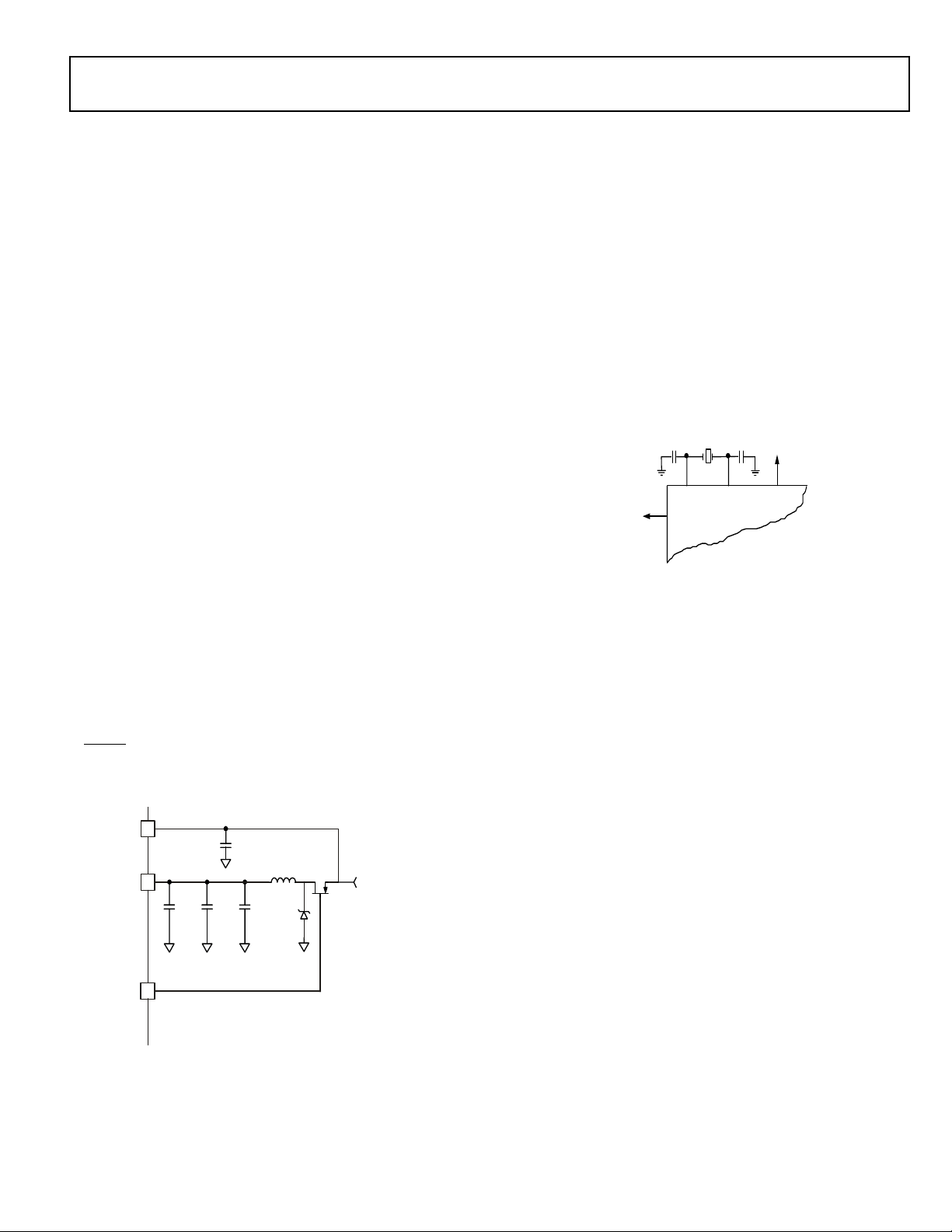
Connect RTC pins RTXI and RTXO with external components
as shown in Figure 4.
Rev. PrD | Page 8 of 60 | January 2005

ADSP-BF534Preliminary Technical Data
RTXI
R1
X1
C1 C2
SUGGESTED COMPONENTS:
ECLIPTEK EC38J (THROUGH-HOLE PACKAGE)
EPSON MC405 12 PF LOAD (SURFACE MOUNT PACKAGE)
C1 = 22 PF
C2 = 22 PF
⍀
R1 = 10 M
NOTE: C1 AND C2 ARE SPECIFIC TO CRYSTAL SPECIFIED FOR X1.
CONTACT CRYSTAL MANUFACTURER FOR DETAILS. C1 AND C2
SPECIFICATIONS ASSUME BOARD TRACE CAPACITANCE OF 3 PF.
Figure 4. External Components for RTC
RTXO
WATCHDOG TIMER
The ADSP-BF534 processor includes a 32-bit timer that can be
used to implement a software watchdog function. A software
watchdog can improve system availability by forcing the processor to a known state through generation of a hardware reset,
non-maskable interrupt (NMI), or general-purpose interrupt, if
the timer expires before being reset by software. The programmer initializes the count value of the timer, enables the
appropriate interrupt, then enables the timer. Thereafter, the
software must reload the counter before it counts to zero from
the programmed value. This protects the system from remaining in an unknown state where software, which would normally
reset the timer, has stopped running due to an external noise
condition or software error.
If configured to generate a hardware reset, the watchdog timer
resets both the core and the ADSP-BF534 processor peripherals.
After a reset, software can determine if the watchdog was the
source of the hardware reset by interrogating a status bit in the
watchdog timer control register.
The timer is clocked by the system clock (SCLK), at a maximum
frequency of f
SCLK
.
TIMERS
There are nine general-purpose programmable timer units in
the ADSP-BF534 processor. Eight timers have an external pin
that can be configured either as a Pulse Width Modulator
(PWM) or timer output, as an input to clock the timer, or as a
mechanism for measuring pulse widths and periods of external
events. These timers can be synchronized to an external clock
input to the several other associated PF pins, an external clock
input to the PPI_CLK input pin, or to the internal SCLK.
The timer units can be used in conjunction with the two UARTs
and the CAN controller to measure the width of the pulses in
the data stream to provide a software auto-baud detect function
for the respective serial channels.
The timers can generate interrupts to the processor core providing periodic events for synchronization, either to the system
clock or to a count of external signals.
In addition to the eight general-purpose programmable timers,
a ninth timer is also provided. This extra timer is clocked by the
internal processor clock and is typically used as a system tick
clock for generation of operating system periodic interrupts.
SERIAL PORTS (SPORTS)
The ADSP-BF534 processor incorporates two dual-channel
synchronous serial ports (SPORT0 and SPORT1) for serial and
multiprocessor communications. The SPORTs support the following features:
2
S capable operation.
•I
• Bidirectional operation – Each SPORT has two sets of independent transmit and receive pins, enabling eight channels
2
of I
S stereo audio.
• Buffered (8-deep) transmit and receive ports – Each port
has a data register for transferring data words to and from
other processor components and shift registers for shifting
data in and out of the data registers.
• Clocking – Each transmit and receive port can either use an
external serial clock or generate its own, in frequencies
ranging from (f
/131,070) Hz to (f
SCLK
SCLK
/2) Hz.
• Word length – Each SPORT supports serial data words
from 3 to 32 bits in length, transferred most-significant-bit
first or least-significant-bit first.
• Framing – Each transmit and receive port can run with or
without frame sync signals for each data word. Frame sync
signals can be generated internally or externally, active high
or low, and with either of two pulsewidths and early or late
frame sync.
• Companding in hardware – Each SPORT can perform
A-law or µ-law companding according to ITU recommendation G.711. Companding can be selected on the transmit
and/or receive channel of the SPORT without additional
latencies.
• DMA operatio ns with single-cyc le overhead – Each SPORT
can automatically receive and transmit multiple buffers of
memory data. The processor can link or chain sequences of
DMA transfers between a SPORT and memory.
• Interrupts – Each transmit and receive port generates an
interrupt upon completing the transfer of a data word or
after transferring an entire data buffer or buffers through
DMA.
• Multichannel capability – Each SPORT supports 128 channels out of a 1024-channel window and is compatible with
the H.100, H.110, MVIP-90, and HMVIP standards.
SERIAL PERIPHERAL INTERFACE (SPI) PORT
The ADSP-BF534 processor has an SPI-compatible port that
enables the processor to communicate with multiple SPI-compatible devices.
The SPI interface uses three pins for transferring data: two data
pins (Master Output-Slave Input, MOSI, and Master InputSlave Output, MISO) and a clock pin (Serial Clock, SCK). An
SPI chip select input pin (SPISS
) lets other SPI devices select the
Rev. PrD | Page 9 of 60 | January 2005

ADSP-BF534 Preliminary Technical Data
processor, and seven SPI chip select output pins (SPISEL7–1) let
the processor select other SPI devices. The SPI select pins are
reconfigured Programmable Flag pins. Using these pins, the SPI
port provides a full-duplex, synchronous serial interface, which
supports both master/slave modes and multimaster
environments.
The SPI port’s baud rate and clock phase/polarities are programmable, and it has an integrated DMA controller,
configurable to support transmit or receive data streams. The
SPI’s DMA controller can only service unidirectional accesses at
any given time.
The SPI port’s clock rate is calculated as:
f
SPI Clock Rate
Where the 16-bit SPI_Baud register contains a value of 2 to
65,535.
During transfers, the SPI port simultaneously transmits and
receives by serially shifting data in and out on its two serial data
lines. The serial clock line synchronizes the shifting and sampling of data on the two serial data lines.
---------------------------------=
2 SPI_Baud×
SCLK
UART PORTS (UARTS)
The ADSP-BF534 processor provides two full-duplex Universal
Asynchronous Receiver/Transmitter (UART) ports, which are
fully compatible with PC-standard UARTs. Each UART port
provides a simplified UART interface to other peripherals or
hosts, supporting full-duplex, DMA-supported, asynchronous
transfers of serial data. A UART port includes support for 5 to
8 data bits, 1 or 2 stop bits, and none, even, or odd parity. Each
UART port supports two modes of operation:
• PIO (Programmed I/O) – The processor sends or receives
data by writing or reading I/O-mapped UART registers.
The data is double-buffered on both transmit and receive.
• DMA (Direct Memory Access) – The DMA controller
transfers both transmit and receive data. This reduces the
number and frequency of interrupts required to transfer
data to and from memory. The UART has two dedicated
DMA channels, one for transmit and one for receive. These
DMA channels have lower default priority than most DMA
channels because of their relatively low service rates.
Each UART port's baud rate, serial data format, error code generation and status, and interrupts are programmable:
• Supporting bit rates ranging from (f
/16) bits per second.
(f
SCLK
• Supporting data formats from 7 to12 bits per frame.
• Both transmit and receive operations can be configured to
generate maskable interrupts to the processor.
The UART port’s clock rate is calculated as:
UART Clock Rate
------------------------------------------------=
16 UART_Divisor×
/ 1,048,576) to
SCLK
f
SCLK
Where the 16-bit UART_Divisor comes from the DLH register
(most significant 8 bits) and DLL register (least significant
8bits).
In conjunction with the general-purpose timer functions, autobaud detection is supported.
The capabilities of the UARTs are further extended with support for the Infrared Data Association (IrDA®) Serial Infrared
Physical Layer Link Specification (SIR) protocol.
CONTROLLER AREA NETWORK (CAN)
The ADSP-BF534 processor offers a CAN controller that is a
communication controller implementing the Controller Area
Network (CAN) 2.0B (active) protocol. This protocol is an asynchronous communications protocol used in both industrial and
automotive control systems. The CAN protocol is well suited for
control applications due to its capability to communicate reliably over a network since the protocol incorporates CRC
checking message error tracking, and fault node confinement.
The ADSP-BF534 CAN controller offers the following features:
• 32 mailboxes (8 receive only, 8 transmit only, 16 configurable for receive or transmit).
• Dedicated acceptance masks for each mailbox.
• Additional data filtering on first two bytes.
• Support for both the standard (11-bit) and extended (29bit) identifier (ID) message formats.
• Support for remote frames.
• Active or passive network support.
• CAN wakeup from Hibernation Mode (lowest static power
consumption mode).
• Interrupts, including: TX Complete, RX Complete, Error,
Global.
The electrical characteristics of each network connection are
very demanding so the CAN interface is typically divided into
two parts: a controller and a transceiver. This allows a single
controller to support different drivers and CAN networks. The
ADSP-BF534 CAN module represents only the controller part
of the interface. The controller interface supports connection to
3.3V high-speed, fault-tolerant, single-wire transceivers.
TWI CONTROLLER INTERFACE
The ADSP-BF534 processor includes a Two Wire Interface
(TWI) module for providing a simple exchange method of control data between multiple devices. The TWI is compatible with
the widely used I
capabilities of simultaneous Master and Slave operation, support for both 7-bit addressing and multimedia data arbitration.
The TWI interface utilizes two pins for transferring clock (SCL)
and data (SDA) and supports the protocol at speeds up to 400k
bits/sec. The TWI interface pins are compatible with 5 V logic
levels.
Additionally, the ADSP-BF534 processor’s TWI module is fully
compatible with Serial Camera Control Bus (SCCB) functionality for easier control of various CMOS camera sensor devices.
2
C bus standard. The TWI module offers the
Rev. PrD | Page 10 of 60 | January 2005

ADSP-BF534Preliminary Technical Data
PORTS
Because of the rich set of peripherals, the ADSP-BF534 processor groups the many peripheral signals to four ports—Port F,
Port G, Port H, and Port J. Most of the associated pins are
shared by multiple signals. The ports function as multiplexer
controls. Eight of the pins (Port F7–0) offer high source/high
sink current capabilities.
General-Purpose I/O (GPIO)
The ADSP-BF534 processor has 48 bi-directional, general-purpose I/O (GPIO) pins
modules
with Port F, Port G, and Port H, respectively. Port J does not
provide GPIO functionality. Each GPIO-capable pin shares
functionality with other ADSP-BF534 processor peripherals via
a multiplexing scheme; however, the GPIO functionality is the
default state of the device upon power-up. Neither GPIO output
or input drivers are active by default. Each general-purpose port
pin can be individually controlled by manipulation of the port
control, status, and interrupt registers:
—PORTFIO, PORTGIO, and PORTHIO, associated
• GPIO Direction Control Register – Specifies the direction
of each individual GPIO pin as input or output.
• GPIO Control and Status Registers – The ADSP-BF534
processor employs a “write one to modify” mechanism that
allows any combination of individual GPIO pins to be
modified in a single instruction, without affecting the level
of any other GPIO pins. Four control registers are provided. One register is written in order to set pin values, one
register is written in order to clear pin values, one register is
written in order to toggle pin values, and one register is
written in order to specify a pin value. Reading the GPIO
status register allows software to interrogate the sense of
the pins.
• GPIO Interrupt Mask Registers – The two GPIO Interrupt
Mask registers allow each individual GPIO pin to function
as an interrupt to the processor. Similar to the two GPIO
Control Registers that are used to set and clear individual
pin values, one GPIO Interrupt Mask Register sets bits to
enable interrupt function, and the other GPIO Interrupt
Mask register clears bits to disable interrupt function.
GPIO pins defined as inputs can be configured to generate
hardware interrupts, while output pins can be triggered by
software interrupts.
• GPIO Interrupt Sensitivity Registers – The two GPIO
Interrupt Sensitivity Registers specify whether individual
pins are level- or edge-sensitive and specify—if edge-sensitive—whether just the rising edge or both the rising and
falling edges of the signal are significant. One register
selects the type of sensitivity, and one register selects which
edges are significant for edge-sensitivity.
allocated across three separate GPIO
PARALLEL PERIPHERAL INTERFACE (PPI)
The ADSP-BF534 processor provides a Parallel Peripheral
Interface (PPI) that can connect directly to parallel A/D and
D/A converters, ITU-R-601/656 video encoders and decoders,
and other general-purpose peripherals. The PPI consists of a
dedicated input clock pin, up to 3 frame synchronization pins,
and up to 16 data pins.
In ITU-R-656 modes, the PPI receives and parses a data stream
of 8-bit or 10-bit data elements. On-chip decode of embedded
preamble control and synchronization information is
supported.
Three distinct ITU-R-656 modes are supported:
•Active Video Only Mode—The PPI does not read in any
data between the End of Active Video (EAV) and Start of
Active Video (SAV) preamble symbols, or any data present
during the vertical blanking intervals. In this mode, the
control byte sequences are not stored to memory; they are
filtered by the PPI.
• Vertical Blanking Only Mode—The PPI only transfers Vertical Blanking Interval (VBI) data, as well as horizontal
blanking information and control byte sequences on VBI
lines.
• Entire Field Mode—The entire incoming bitstream is read
in through the PPI. This includes active video, control preamble sequences, and ancillary data that may be embedded
in horizontal and vertical blanking intervals.
Though not explicitly supported, ITU-R-656 output functionality can be achieved by setting up the entire frame structure
(including active video, blanking, and control information) in
memory and streaming the data out the PPI in a frame sync-less
mode. The processor’s 2D DMA features facilitate this transfer
by allowing the static frame buffer (blanking and control codes)
to be placed in memory once, and simply updating the active
video information on a per-frame basis.
The general-purpose modes of the PPI are intended to suit a
wide variety of data capture and transmission applications. The
modes are divided into four main categories, each allowing up
to 16 bits of data transfer per PPI_CLK cycle:
• Data Receive with Internally Generated Frame Syncs.
• Data Receive with Externally Generated Frame Syncs.
• Data Transmit with Internally Generated Frame Syncs
• Data Transmit with Externally Generated Frame Syncs
These modes support ADC/DAC connections, as well as video
communication with hardware signalling. Many of the modes
support more than one level of frame synchronization. If
desired, a programmable delay can be inserted between assertion of a frame sync and reception/transmission of data.
DYNAMIC POWER MANAGEMENT
The ADSP-BF534 processor provides five operating modes,
each with a different performance/power profile. In addition,
Dynamic Power Management provides the control functions to
dynamically alter the processor core supply voltage, further
reducing power dissipation. Control of clocking to each of the
ADSP-BF534 processor peripherals also reduces power consumption. See Table 4 for a summary of the power settings for
each mode.
Rev. PrD | Page 11 of 60 | January 2005

ADSP-BF534 Preliminary Technical Data
Full-On Operating Mode – Maximum Performance
In the Full-On mode, the PLL is enabled and is not bypassed,
providing capability for maximum operational frequency. This
is the power-up default execution state in which maximum performance can be achieved. The processor core and all enabled
peripherals run at full speed.
Active Operating Mode – Moderate Power Savings
In the Active mode, the PLL is enabled but bypassed. Because
the PLL is bypassed, the processor’s core clock (CCLK) and system clock (SCLK) run at the input clock (CLKIN) frequency. In
this mode, the CLKIN to CCLK multiplier ratio can be changed,
although the changes are not realized until the Full-On mode is
entered. DMA access is available to appropriately configured L1
memories.
In the Active mode, it is possible to disable the PLL through the
PLL Control register (PLL_CTL). If disabled, the PLL must be
re-enabled before transitioning to the Full-On or Sleep modes.
Table 4. Power Settings
Mode
Full On Enabled No Enabled Enabled On
Active Enabled/
Sleep Enabled - Disabled Enabled On
Deep Sleep Disabled - Disabled Disabled On
Hibernate Disabled - Disabled Disabled Off
PLL
Disabled
PLL
Bypassed
Core
Clock
(CCLK)
System
Clock
(SCLK)
Ye s E na bl ed E na b le d On
Core
Sleep Operating Mode – High Dynamic Power Savings
The Sleep mode reduces dynamic power dissipation by disabling the clock to the processor core (CCLK). The PLL and
system clock (SCLK), however, continue to operate in this
mode. Typically an external event or RTC activity will wake up
the processor. When in the Sleep mode, assertion of wakeup will
cause the processor to sense the value of the BYPASS bit in the
PLL Control register (PLL_CTL). If BYPASS is disabled, the
processor will transition to the Full On mode. If BYPASS is
enabled, the processor will transition to the Active mode.
When in the Sleep mode, system DMA access to L1 memory is
not supported.
Deep Sleep Operating Mode – Maximum Dynamic Power
Savings
The Deep Sleep mode maximizes dynamic power savings by
disabling the clocks to the processor core (CCLK) and to all synchronous peripherals (SCLK). Asynchronous peripherals, such
as the RTC, may still be running but will not be able to access
internal resources or external memory. This powered-down
mode can only be exited by assertion of the reset interrupt
(RESET
) or by an asynchronous interrupt generated by the
RTC. When in Deep Sleep mode, an RTC asynchronous inter-
rupt causes the processor to transition to the Active mode.
Assertion of RESET
while in Deep Sleep mode causes the pro-
cessor to transition to the Full On mode.
Hibernate Operating Mode – Maximum Static Power
Savings
The hibernate mode maximizes static power savings by disabling the voltage and clocks to the processor core (CCLK) and
to all the synchronous peripherals (SCLK). The internal voltage
regulator for the processor can be shut off by writing b#00 to the
FREQ bits of the VR_CTL register. This disables both CCLK
and SCLK. Furthermore, it sets the internal power supply voltage (V
) to 0V to provide the greatest power savings mode.
DDINT
Any critical information stored internally (memory contents,
register contents, etc.) must be written to a non-volatile storage
device prior to removing power if the processor state is to be
preserved.
Since V
is still supplied in this mode, all of the external
DDEXT
pins tri-state, unless otherwise specified. This allows other
devices that may be connected to the processor to have power
still applied without drawing unwanted current.
The internal supply regulator can be woken up by CAN. It can
also be woken up by a Real-Time Clock wakeup event or by
Power
asserting the RESET
reset sequence.
pin, both of which initiate the hardware
Power Savings
As shown in Table 5, the ADSP-BF534 processor supports three
different power domains. The use of multiple power domains
maximizes flexibility, while maintaining compliance with
industry standards and conventions. By isolating the internal
logic of the ADSP-BF534 processor into its own power domain,
separate from the RTC and other I/O, the processor can take
advantage of Dynamic Power Management, without affecting
the RTC or other I/O devices. There are no sequencing requirements for the various power domains.
Table 5. Power Domains
Power Domain VDD Range
All internal logic, except RTC V
RTC internal logic and crystal I/O V
All other I/O V
DDINT
DDRTC
DDEXT
The power dissipated by a processor is largely a function of the
clock frequency of the processor and the square of the operating
voltage. For example, reducing the clock frequency by 25%
results in a 25% reduction in power dissipation, while reducing
the voltage by 25% reduces power dissipation by more than
40%. Further, these power savings are additive, in that if the
clock frequency and supply voltage are both reduced, the power
savings can be dramatic.
The Dynamic Power Management feature of the ADSP-BF534
processor allows both the processor’s input voltage (V
clock frequency (f
) to be dynamically controlled.
CCLK
DDINT
) and
Rev. PrD | Page 12 of 60 | January 2005
ADSP-BF534Preliminary Technical Data
As explained above, the savings in power dissipation can be
modeled by the following equations:
Power Savings Factor
f
CCLKRED
--------------------------------
=
f
CCLKNOM
V
DDINTRED
--------------------------------------
×
V
DDINTNOM
2
T
×
RED
------------------
T
NOM
% Power Savings 1 Power Savings Factor–()100%×=
where the variables in the equations are:
•f
•f
•V
•V
•T
•T
is the nominal core clock frequency
CCLKNOM
is the reduced core clock frequency
CCLKRED
DDINTNOM
DDINTRED
NOM
RED
is the nominal internal supply voltage
is the reduced internal supply voltage
is the duration running at f
is the duration running at f
CCLKNOM
CCLKRED
VOLTAGE REGULATION
The ADSP-BF534 processor provides an on-chip voltage regulator that can generate processor core voltage levels (0.85V to
1.2V guaranteed from -5% to 10%) from an external 2.25 V to
3.6 V supply. Figure 5 shows the typical external components
required to complete the power management system. The regulator controls the internal logic voltage levels and is
programmable with the Voltage Regulator Control Register
(VR_CTL) in increments of 50 mV. To reduce standby power
consumption, the internal voltage regulator can be programmed
to remove power to the processor core while keeping I/O power
supplied. While in Hibernate mode, V
eliminating the need for external buffers. The voltage regulator
can be activated from this power down state by assertion of the
RESET
pin, which will then initiate a boot sequence. The regula-
tor can also be disabled and bypassed at the user’s discretion.
V
DDEXT
100 µF
10 µH
0.1 µF
ZHCS1000
EXTERNAL COMPONEN TS
VR
V
DDINT
OUT
100 µF
1µF
1-0
NOTE: VR
AND DESIG NER SHOULD MI NIMIZE TRACE L ENGTH TO FDS943 1A.
1-0 S HOULD BE TIED T OGETHER EXTERNALLY
OUT
can still be applied,
DDEXT
2.25V - 3.6V
INPU T VOLTA GE
RANGE
FDS9431A
CLOCK SIGNALS
The ADSP-BF534 processor can be clocked by an external crystal, a sine wave input, or a buffered, shaped clock derived from
an external clock oscillator.
If an external clock is used, it should be a TTL compatible signal
and must not be halted, changed, or operated below the specified frequency during normal operation. This signal is
connected to the processor’s CLKIN pin. When an external
clock is used, the XTAL pin must be left unconnected.
Alternatively, because the ADSP-BF534 processor includes an
on-chip oscillator circuit, an external crystal may be used. The
crystal should be connected across the CLKIN and XTAL pins,
with two capacitors connected as shown in Figure 6. Capacitor
values are dependent on crystal type and should be specified by
the crystal manufacturer. A parallel-resonant, fundamental frequency, microprocessor-grade crystal should be used.
CLKI N
CLKBUF
Figure 6. External Crystal Connections
PROCESSOR
The CLKBUF pin is an output pin, and is a buffer version of the
input clock. The Blackfin core is running at a different clock rate
than the on-chip peripherals. As shown in Figure 7 on page 14,
the core clock (CCLK) and system peripheral clock (SCLK) are
derived from the input clock (CLKIN) signal. An on-chip PLL is
capable of multiplying the CLKIN signal by a user programmable 1x to 63x multiplication factor (bounded by specified
minimum and maximum VCO frequencies). The default multiplier is 10x, but it can be modified by a software instruction
sequence. On-the-fly frequency changes can be effected by simply writing to the PLL_DIV register.
On-the-fly CCLK and SCLK frequency changes can be effected
by simply writing to the PLL_DIV register. Whereas the maximum allowed CCLK and SCLK rates depend on the applied
voltages V
DDINT
and V
, the VCO is always permitted to run
DDEXT
up to the frequency specified by the part’s speed grade. The
CLKOUT pin reflects the SCLK frequency to the off-chip world.
It belongs to the SDRAM interface, but it functions as reference
signal in other timing specifications as well. While active by
default, it can be disabled by the EBIU_SDGCTL and
EBIU_AMGCTL registers.
All on-chip peripherals are clocked by the system clock (SCLK).
The system clock frequency is programmable by means of the
SSEL3–0 bits of the PLL_DIV register. The values programmed
CLKOUTXTAL
Figure 5. Voltage Regulator Circuit
Rev. PrD | Page 13 of 60 | January 2005
ADSP-BF534 Preliminary Technical Data
DYNAMIC MODIFICATION
RE QUIRES PL L SEQU ENC ING
CLKI N
PLL
.5x - 64x
Figure 7. Frequency Modification Methods
SCLK CC LK
SCLK 133MHZ
DYNAM IC MODIFICATIO N
+ 1 , 2, 4, 8
VCO
ON-THE-FLY
+ 1:15
CCLK
SCLK
into the SSEL fields define a divide ratio between the PLL output
(VCO) and the system clock. SCLK divider values are 1 through
15. Table 6 illustrates typical system clock ratios:
Table 6. Example System Clock Ratios
Signal Name
SSEL3–0
Divider Ratio
VCO/SCLK
Example Frequency Ratios
(MHz)
VCO SCLK
0001 1:1 100 100
0110 6:1 300 50
1010 10:1 500 50
Note that the divisor ratio must be chosen to limit the system
clock frequency to its maximum of f
. The SSEL value can be
SCLK
changed dynamically without any PLL lock latencies by writing
the appropriate values to the PLL divisor register (PLL_DIV).
The core clock (CCLK) frequency can also be dynamically
changed by means of the CSEL1–0 bits of the PLL_DIV register.
Supported CCLK divider ratios are 1, 2, 4, and 8, as shown in
Table 7. This programmable core clock capability is useful for
fast core frequency modifications.
The maximum CCLK frequency not only depends on the part's
speed grade (see page 60), it also depends on the applied V
DDINT
voltage. See Table 10 - Table 11 for details. The maximal system
clock rate (SCLK) depends on the chip package and the applied
V
voltage (see Table 13).
DDEXT
Table 7. Core Clock Ratios
Signal Name
CSEL1–0
Divider Ratio
VCO/CCLK
Example Frequency Ratios
VCO CCLK
00 1:1 300 300
01 2:1 300 150
10 4:1 500 125
11 8:1 200 25
BOOTING MODES
The ADSP-BF534 processor has six mechanisms (listed in
Table 8) for automatically loading internal and external mem-
ory after a reset. A seventh mode is provided to execute from
external memory, bypassing the boot sequence.
Table 8. Booting Modes
BMODE2–0 Description
000 Execute from 16-bit external memory
(Bypass Boot ROM)
001 Boot from 8-bit or 16-bit memory
(EPROM/flash)
010 Reserved
011 Boot from serial SPI memory (EEPROM/flash)
100 Boot from SPI host (slave mode)
101 Boot from serial TWI memory
(EEPROM/flash)
110 Boot from TWI host (slave mode)
111 Boot from UART host (slave mode)
The BMODE pins of the Reset Configuration Register, sampled
during power-on resets and software-initiated resets, implement the following modes:
• Execute from 16-bit external memory – Execution starts
from address 0x2000 0000 with 16-bit packing. The boot
ROM is bypassed in this mode. All configuration settings
are set for the slowest device possible (3-cycle hold time;
15-cycle R/W access times; 4-cycle setup).
• Boot from 8-bit and 16-bit external flash memory – The
8-bit or 16-bit flash boot routine located in boot ROM
memory space is set up using Asynchronous Memory Bank
0. All configuration settings are set for the slowest device
possible (3-cycle hold time; 15-cycle R/W access times;
4-cycle setup). The boot ROM evaluates the first byte of the
boot stream at address 0x2000 0000. If it is 0x40, 8-bit boot
is performed. A 0x60 byte is required for 16-bit boot.
• Boot from serial SPI memory (EEPROM or flash). Eight-,
16-, or 24-bit addressable devices are supported as well as
AT45DB041, AT45DB081, and AT45DB161 data flash
devices from Atmel. The SPI uses the PF10/SPI SSEL1 output pin to select a single SPI EEPROM/flash device,
submits a read command and successive address bytes
(0x00) until a valid 8-, 16-, or 24-bit, or Atmel addressable
device is detected, and begins clocking data into the
processor.
• Boot from SPI host device – The Blackfin processor operates in SPI slave mode and is configured to receive the bytes
of the .LDR file from an SPI host (master) agent. To hold
off the host device from transmitting while the boot ROM
is busy, the Blackfin processor will assert a flag pin to signal
the host device not to send any more bytes until the flag is
de-asserted. The flag is chosen by the user and this information will be transferred to the Blackfin processor via bits
8:5 of the FLAG header.
Rev. PrD | Page 14 of 60 | January 2005

ADSP-BF534Preliminary Technical Data
• Boot from UART – Using an autobaud handshake
sequence, a boot-stream-formatted program is downloaded
by the Host. The Host agent selects a baud rate within the
UART’s clocking capabilities. When performing the autobaud, the UART expects a “@” (boot stream) character
(eight bits data, one start bit, one stop bit, no parity bit) on
the RXD pin to determine the bit rate. It then replies with
an acknowledgement which is composed of 4 bytes: 0xBF,
the value of UART_DLL, the value of UART_DLH, 0x00.
The Host can then download the boot stream. When the
processor needs to hold off the Host, it de-asserts CTS.
Therefore, the Host must monitor this signal.
• Boot from serial TWI memory (EEPROM/flash) – The
Blackfin processor operates in master mode and selects the
TWI slave with the unique id 0xA0. It submits successive
read commands to the memory device starting at two byte
internal address 0x0000 and begins clocking data into the
processor. The TWI memory device should comply with
Philips I
bility to auto-increment its internal address counter such
that the contents of the memory device can be read
sequentially.
• Boot from TWI Host – The TWI Host agent selects the
slave with the unique id 0x5F. The processor replies with an
acknowledgement and the Host can then download the
boot stream. The TWI Host agent should comply with
Philips I
plexer can be used to select one processor at a time when
booting multiple processors from a single TWI.
For each of the boot modes, a 10-byte header is first brought in
from an external device. The header specifies the number of
bytes to be transferred and the memory destination address.
Multiple memory blocks may be loaded by any boot sequence.
Once all blocks are loaded, program execution commences from
the start of L1 instruction SRAM.
In addition, bit 4 of the Reset Configuration Register can be set
by application code to bypass the normal boot sequence during
a software reset. For this case, the processor jumps directly to
the beginning of L1 instruction memory.
To augment the boot modes, a secondary software loader can be
added to provide additional booting mechanisms. This secondary loader could provide the capability to boot from flash,
variable baud rate, and other sources. In all boot modes except
Bypass, program execution starts from on-chip L1 memory
address 0xFFA0 0000.
2
C Bus Specification version 2.1 and have the capa-
2
C Bus Specification version 2.1. An I2C multi-
INSTRUCTION SET DESCRIPTION
The Blackfin processor family assembly language instruction set
employs an algebraic syntax designed for ease of coding and
readability. The instructions have been specifically tuned to provide a flexible, densely encoded instruction set that compiles to
a very small final memory size. The instruction set also provides
fully featured multifunction instructions that allow the programmer to use many of the processor core resources in a single
instruction. Coupled with many features more often seen on
microcontrollers, this instruction set is very efficient when compiling C and C++ source code. In addition, the architecture
supports both user (algorithm/application code) and supervisor
(O/S kernel, device drivers, debuggers, ISRs) modes of operation, allowing multiple levels of access to core processor
resources.
The assembly language, which takes advantage of the processor’s unique architecture, offers the following advantages:
• Seamlessly integrated DSP/MCU features are optimized for
both 8-bit and 16-bit operations.
• A multi-issue load/store modified-Harvard architecture,
which supports two 16-bit MAC or four 8-bit ALU + two
load/store + two pointer updates per cycle.
• All registers, I/O, and memory are mapped into a unified
4G byte memory space, providing a simplified programming model.
• Microcontroller features, such as arbitrary bit and bit-field
manipulation, insertion, and extraction; integer operations
on 8-, 16-, and 32-bit data-types; and separate user and
supervisor stack pointers.
• Code density enhancements, which include intermixing of
16- and 32-bit instructions (no mode switching, no code
segregation). Frequently used instructions are encoded in
16 bits.
DEVELOPMENT TOOLS
The ADSP-BF534 processor is supported with a complete set of
CROSSCORE® software and hardware development tools,
including Analog Devices emulators and VisualDSP++® development environment. The same emulator hardware that
supports other Blackfin processors also fully emulates the
ADSP-BF534 processor.
DESIGNING AN EMULATOR-COMPATIBLE PROCESSOR BOARD (TARGET)
The Analog Devices family of emulators are tools that every system developer needs to test and debug hardware and software
systems. Analog Devices has supplied an IEEE 1149.1 JTAG
Test Access Port (TAP) on each JTAG processor. The emulator
uses the TAP to access the internal features of the processor,
allowing the developer to load code, set breakpoints, observe
variables, observe memory, and examine registers. The processor must be halted to send data and commands, but once an
operation has been completed by the emulator, the processor
system is set running at full speed with no impact on system
timing.
To use these emulators, the target board must include a header
that connects the processor’s JTAG port to the emulator.
For details on target board design issues including mechanical
layout, single processor connections, multiprocessor scan
chains, signal buffering, signal termination, and emulator pod
logic, see Analog Devices JTAG Emulation Technical Reference
(EE-68) on the Analog Devices web site under
www.analog.com/ee-notes. This document is updated regularly
to keep pace with improvements to emulator support.
Rev. PrD | Page 15 of 60 | January 2005

ADSP-BF534 Preliminary Technical Data
RELATED DOCUMENTS
The following publications that describe the ADSP-BF534 processors (and related processors) can be ordered from any
Analog Devices sales office or accessed electronically on our
web site:
• ADSP-BF537 Blackfin Processor Hardware Reference
• Blackfin Processor Programming Reference
• ADSP-BF534 Blackfin Processor Anomaly List
Rev. PrD | Page 16 of 60 | January 2005

PIN DESCRIPTIONS
ADSP-BF534Preliminary Technical Data
ADSP-BF534 processor pin definitions are listed in Table 9. In
order to maintain maximum functionality and reduce package
size and pin count, some pins have dual, multiplexed functionality. In cases where pin functionality is reconfigurable, the
default state is shown in plain text, while alternate functionality
is shown in italics. Pins shown with an asterisk after their name
(*) offer high source/high sink current capabilities.
All pins are tristated during and immediately after reset with the
exception of the external memory interface. On the external
memory interface, the control and address lines are driven high
during reset unless the BR
pin is asserted.
All I/O pins have their input buffers disabled with the exception
of the pins noted in the data sheet that need pullups or pulldowns if unused.
Table 9. Pin Descriptions
Pin Name I/O Function Driver Type
Memory Interface
ADDR19–1 O Address Bus for Async Access A
DATA15–0 I/O Data Bus for Async/Sync Access A
ABE1–0
/SDQM1–0 O Byte Enables/Data Masks for Async/Sync Access A
2
BR
BG
BGH
Asynchronous Memory Control
AMS
3–0 O Bank Select A
ARDY I Hardware Ready Control
AOE
ARE
AWE
Synchronous Memory Control
SRAS
SCAS
SWE
SCKE O Clock Enable A
CLKOUT O Clock Output B
SA10 O A10 Pin A
SMS
Port F: GPIO/UART1–0/Timer7–0/External DMA Request (* = High Source/High Sink Pin)
PF0* - GPIO/UART0 TX/DMAR0 I/O GPIO/UART0 Transmit/DMA Request 0 C
PF1*- GPIO/UART0 RX/DMAR1/TAC I1 I/O GPIO/UART0 Receive/DMA Request 1/Timer1 Alternate Input Capture C
PF2* - GPIO/UART1 TX/TMR7 I/O GPIO/UART1 Transmit/Timer7 C
PF3* - GPIO/UART1 RX/TMR6/TA CI6 I/O GPIO/UART1 Receive/Timer6/Timer6 Alternate Input Capture C
PF4* - GPIO/TMR5/SPI SSEL6 I/O GPIO/Timer5/SPI Slave Select Enable 6 C
PF5* - GPIO/TMR4/SPI SSEL5 I/O GPIO/Timer4/SPI Slave Select Enable 5 C
PF6* - GPIO/TMR3/SPI SSEL4 I/O GPIO/Timer3/SPI Slave Select Enable 4 C
PF7* - GPIO/TMR2/PPI FS3 I/O GPIO/Timer2/PPI Frame Sync 3 C
PF8 - GPIO/TMR1/PPI FS2 I/O GPIO/Timer1/PPI Frame Sync 2 D
PF9 - GPIO/TMR0/PPI FS1 I/O GPIO/Timer0/PPI Frame Sync 1 D
PF10 - GPIO/SPI SSEL1 I/O GPIO/SPI Slave Select Enable 1 D
PF11 - GPIO/SPI MOSI I/O GPIO/SPI Master Out Slave In D
IBus Request
OBus Grant A
O Bus Grant Hang A
O Output Enable A
ORead Enable A
OWrite Enable A
O Row Address Strobe A
O Column Address Strobe A
OWrite Enable A
O Bank Select A
1
Rev. PrD | Page 17 of 60 | January 2005

ADSP-BF534 Preliminary Technical Data
Table 9. Pin Descriptions (Continued)
Pin Name I/O Function Driver Type
Port F: GPIO/UART1–0/Timer7–0/External DMA Request (* = High Source/High Sink Pin), continued
PF12 - GPIO/SPI MISO
PF13 - GPIO/SPI SCK I/O GPIO/SPI Clock D
PF14 - GPIO/SPI SS/TACLK0 I/O GPIO/SPI Slave Select/Alternate Timer0 Clock Input D
PF15 - GPIO/PPI CLK/TMRCLK I/O GPIO/PPI Clock/External Timer Reference D
Port G: GPIO/PPI/SPORT1
PG0 - GPIO/PPI D0 I/O GPIO/PPI Data 0 D
PG1 - GPIO/PPI D1 I/O GPIO/PPI Data 1 D
PG2 - GPIO/PPI D2 I/O GPIO/PPI Data 2 D
PG3 - GPIO/PPI D3 I/O GPIO/PPI Data 3 D
PG4 - GPIO/PPI D4 I/O GPIO/PPI Data 4 D
PG5 - GPIO/PPI D5 I/O GPIO/PPI Data 5 D
PG6 - GPIO/PPI D6 I/O GPIO/PPI Data 6 D
PG7 - GPIO/PPI D7 I/O GPIO/PPI Data 7 D
PG8 - GPIO/PPI D8/DR1SEC I/O GPIO/PPI Data 8/SPORT1 Receive Data Secondary D
PG9 - GPIO/PPI D9/DT1SEC I/O GPIO/PPI Data 9/SPORT1 Transmit Data Secondary D
PG10 - GPIO/PPI D10/RSCLK1 I/O GPIO/PPI Data 10/SPORT1 Receive Serial Clock D
PG11 - GPIO/PPI D11/RFS1 I/O GPIO/PPI Data 11/SPORT1 Receive Frame Sync D
PG12 - GPIO/PPI D12/DR1PRI I/O GPIO/PPI Data 12/SPORT1 Receive Data Primary D
PG13 - GPIO/PPI D13/TSCLK1 I/O GPIO/PPI Data 13/SPORT1 Transmit Serial Clock D
PG14 - GPIO/PPI D14/TFS1 I/O GPIO/PPI Data 14/SPORT1 Transmit Frame Sync D
PG15 - GPIO/PPI D15/DT1PRI I/O GPIO/PPI Data 15/SPORT1 Transmit Data Primary D
Port H: GPIO
PH0 - GPIO I/O GPIO D
PH1 - GPIO I/O GPIO D
PH2 - GPIO I/O GPIO D
PH3 - GPIO I/O GPIO D
PH4 - GPIO I/O GPIO D
PH5 - GPIO I/O GPIO D
PH6 - GPIO I/O GPIO D
PH7 - GPIO I/O GPIO D
PH8 - GPIO I/O GPIO D
PH9 - GPIO I/O GPIO D
PH10 - GPIO I/O GPIO D
PH11 - GPIO I/O GPIO D
PH12 - GPIO I/O GPIO D
PH13 - GPIO I/O GPIO D
PH14 - GPIO I/O GPIO D
PH15 - GPIO I/O GPIO D
3
I/O GPIO/SPI Master In Slave Out D
1
Rev. PrD | Page 18 of 60 | January 2005

ADSP-BF534Preliminary Technical Data
Table 9. Pin Descriptions (Continued)
Pin Name I/O Function Driver Type
Port J:SPORT0/TWI/SPI Select/CAN
PJ0 - No connect No Connect
PJ1 - Connect to GND G Connect to GND
PJ2 - SCL I/O TWI Serial Clock D
PJ3 - SDA I/O TWI Serial Data D
PJ4 - DR0SEC/CANRX/TA CI 0 I SPORT0 Receive Data Secondary/CAN Receive/Timer0 Alternate Input
Capture
PJ5 - DT0SEC/CANTX/SPI SSEL7 O SPORT0 Transmit Data Secondary/CAN Transmit/SPI Slave Select
Enable 7
PJ6 - RS CLK0/TACLK2 I/O SPORT0 Receive Serial Clock/Alternate Timer2 Clock Input E
PJ7 - RFS0/TACLK3 I/O SPORT0 Receive Frame Sync/Alternate Timer3 Clock Input D
PJ8 - DR0PRI/TACLK4 I SPORT0 Receive Data Primary/Alternate Timer4 Clock Input
PJ9 - TS CLK0/TACLK1 I/O SPORT0 Transmit Serial Clock/Alternate Timer1 Clock Input E
PJ10 - TFS0/SPI SSEL3 I/O SPORT0 Transmit Frame Sync/SPI Slave Select Enable 3 D
PJ11 - DT0PRI/SPI SSEL2 O SPORT0 Transmit Data Primary/SPI Slave Select Enable 2 D
Real Time Clock
4
RTXI
I RTC Crystal Input
RTXO O RTC Crystal Output
JTAG Port
TCK I JTAG Clock
TDO O JTAG Serial Data Out D
TDI I JTAG Serial Data In
TMS I JTAG Mode Select
5
TRST
EMU
IJTAG Reset
O Emulation Output D
Clock
CLKIN I Clock/Crystal Input
XTAL O Crystal Output
CLKBUF O Buffered CLKIN Output
Mode Controls
RESET
NMI
6
I Reset
I Non-maskable Interrupt
BMODE2–0 I Boot Mode Strap 2-0
Voltage Regulator
VROUT0 O External FET Drive
VROUT1 O External FET Drive
Supplies
V
V
V
DDEXT
DDINT
DDRTC
PI/O Power Supply
P Internal Power Supply (regulated from 2.25V to 3.6V)
P Real Time Clock Power Supply
GND G External Ground
1
See “Output Drive Currents” on page 46 for more information about each driver types.
2
This pin should be pulled HIGH when not used.
3
This pin should always be pulled HIGH through a 4.7 K Ohms resistor if booting via the SPI port.
4
This pin should always be pulled LOW when not used.
5
This pin should be pulled LOW if the JTAG port will not be used.
6
This pin should always be pulled HIGH when not used.
D
1
Rev. PrD | Page 19 of 60 | January 2005

ADSP-BF534 Preliminary Technical Data
SPECIFICATIONS
Note that component specifications are subject to change
without notice.
RECOMMENDED OPERATING CONDITIONS
Parameter
V
DDINT
V
DDEXT
V
DDRTC
V
IH
V
IHCLKIN
V
IH5V
V
IL
V
IL5V
T
A
1
Specifications subject to change without notice.
2
Voltage regulator output is guaranteed from -5% to 10% of specified values.
3
The ADSP-BF534 processor is 3.3 V tolerant (always accepts up to 3.6 V maximum VIH), but voltage compliance (on outputs, VOH) depends on the input V
(maximum) approximately equals V
RFS0) and input only pins (BR
4
Parameter value applies to all input and bi-directional pins except CLKIN, SDA, and SCL.
5
Parameter value applies to CLKIN pin only.
6
Certain ADSP-BF534 processor pins are 5.0 V tolerant (always accept up to 5.5 V maximum VIH), but voltage compliance (on outputs, VOH) depends on the input V
because V
therefore require a pullup resistor. Consult the I
7
Parameter value applies to all input and bi-directional pins except SDA and SCL.
1
Internal Supply Voltage
External Supply Voltage 2.25 2.5 or 3.3 3.6 V
Real Time Clock Power Supply Voltage 2.25 3.6 V
High Level Input Voltage
High Level Input Voltage5, @ V
High Level Input Voltage6, @ V
Low Level Input Voltage
Low Level Input Voltage6, @ V
Ambient Operating Temperature
Automotive –40 105 ºC
Industrial –40 85 ºC
(maximum). This 3.3 V tolerance applies to bi-directional pins (DATA15–0, PF15–0, PG15–0, PH15–0, TFS0, TCLK0, RSCLK0,
DDEXT
, ARDY, DR0PRI, DR0SEC, RTXI, TCK, TDI, TMS, TRST, CLKIN, RESET, NMI, and BMODE2–0).
(maximum) approximately equals V
OH
2
3, 4
, @ V
3, 7
, @ V
(maximum). This 5.0 V tolerance applies to SDA and SCL pins only. The SDA and SCL pins are open drain and
DDEXT
2
C specification version 2.1 for the proper resistor value.
=maximum
DDEXT
=maximum
DDEXT
=maximum
DDEXT
=minimum
DDEXT
=minimum –0.3 0.8 V
DDEXT
0.8 1.2 1.32 V
2.0 3.6 V
2.2 3.6 V
2.0 5.0 V
–0.3 0.6 V
Minimum Nominal Maximum Unit
, because VOH
DDEXT
DDEXT
,
Rev. PrD | Page 20 of 60 | January 2005

ADSP-BF534Preliminary Technical Data
ELECTRICAL CHARACTERISTICS
Parameter
V
OH
Port F7–0 @ V
Port F15–8, Port G, Port H I
Max Combined for Port F7–0 TBD V
Max Total for all Port F, Port G,
and Port H Pins
V
OL
Port F7–0 @ V
Port F15–8, Port G, Port H I
Max Combined for Port F7–0 TBD V
Max Total for all Port F, Port G,
and Port H Pins
I
IH
I
IL
I
OZH
I
OZL
Max Total Current for all Port F,
Port G, and Port H Pins
C
IN
1
Specifications subject to change without notice.
2
Applies to output and bidirectional pins.
3
Applies to input pins.
4
Applies to three-statable pins.
5
Applies to all signal pins.
6
Guaranteed, but not tested.
1
Test Conditions Min Max Unit
High Level Output Voltage2
= 3.3V +/- 10%, IOH = –10 mA
DDEXT
@ V
OH
= 2.5V +/- 10%, IOH = –6 mA
DDEXT
= –1 mA V
– 0.5V
V
DDEXT
V
– 0.5V
DDEXT
– 0.5V V
DDEXT
TBD V
Low Level Output Voltage
2
= 3.3V +/- 10%, IOL = 10 mA
DDEXT
@ V
OL
= 2.5V +/- 10%, IOL = 6 mA
DDEXT
= 2 mA 0.5V V
0.5V
0.5V
TBD V
High Level Input Current
Low Level Input Current4@ V
Three-State Leakage
4
Current
Three-State Leakage
5
Current
3
@ V
@ V
@ V
=maximum, VIN = VDD maximum TBD µA
DDEXT
=maximum, VIN = 0 V TBD µA
DDEXT
= maximum, VIN = VDD maximum TBD µA
DDEXT
= maximum, VIN = 0 V TBD µA
DDEXT
TBD mA
Input Capacitance
5, 6
fIN = 1 MHz, T
= 25°C, VIN = 2.5 V TBD pF
A
MBIENT
V
V
V
V
Rev. PrD | Page 21 of 60 | January 2005

ADSP-BF534 Preliminary Technical Data
ABSOLUTE MAXIMUM RATINGS
Internal (Core) Supply Voltage1 (V
External (I/O) Supply Voltage
Input Voltage
1
Output Voltage Swing
Load Capacitance
1,2
Storage Temperature Range
1
1
1
Junction Temperature Underbias
1
Stresses greater than those listed above may cause permanent damage to the device. These
are stress ratings only. Functional operation of the device at these or any other conditions
greater than those indicated in the operational sections of this specification is not implied.
Exposure to absolute maximum rating conditions for extended periods may affect device
reliability.
2
For proper SDRAM controller operation, the maximum load capacitance is 50 pF (at 3.3V)
or 30 pF (at 2.5V) for ADDR19–1, DATA15–0, ABE1–0
SA10, SRAS
, SCAS, SWE, and SMS.
)
DDINT
(V
)–0.3 V to +3.8 V
DDEXT
–0.3 V to + 1.4 V
–0.5 V to +3.6 V
–0.5 V to V
200 pF
–65ºC to +150ºC
1
+125ºC
/SDQM1–0, CLKOUT, SCKE,
DDEXT
a
PRODUCT
+0.5 V
LOT NUMBER
DATE CODE
Figure 8. Product Information on Package
ESD SENSITIVITY
CAUTION
ESD (electrostatic discharge) sensitive device. Electrostatic charges as high as 4000V readily
accumulate on the human body and test equipment and can discharge without detection. Although
the ADSP-BF534 processor features proprietary ESD protection circuitry, permanent damage may
occur on devices subjected to high-energy electrostatic discharges. Therefore, proper ESD precautions are recommended to avoid performance degradation or loss of functionality.
ADSP-BF534
SBBC 2Z 500X
367334.1 0.2
0440 SINGAPORE
B
S = INTERNAL VOLTAGE
B = TEMP RANGE
BC2Z = PACKAGE
500 = SPEED GRADE
X = X-GRADE PART
SILICON REVISION
ASSEMBLY
Rev. PrD | Page 22 of 60 | January 2005

TIMING SPECIFICATIONS
Table 10 and Table 11 describe the timing requirements for the
ADSP-BF534 processor clocks. Take care in selecting MSEL,
SSEL, and CSEL ratios so as not to exceed the maximum core
clock and system clock. Table 12 describes Phase-Locked Loop
operating conditions.
ADSP-BF534Preliminary Technical Data
Table 10. Core Clock Requirements—500 MHz Speed Grade
1
Parameter Minimum Maximum Unit
f
CCLK
f
CCLK
f
CCLK
f
CCLK
f
CCLK
1
The speed grade of a given part is printed on the chip’s package as shown in Figure 8 on page 22 and can also be seen on the “Ordering Guide” on page 60. It stands for the
Maximum allowed CCLK frequency at VDDINT = 1.2V and the maximum allowed VCO frequency at any supply voltage.
Table 11. Core Clock Requirements—400 MHz Speed Grade
Core Clock Frequency (V
Core Clock Frequency (V
Core Clock Frequency (V
Core Clock Frequency (V
Core Clock Frequency (V
=1.2 V–5%) 500 MHz
DDINT
=1.1 V–5%) TBD MHz
DDINT
=1.0 V–5%) TBD MHz
DDINT
=0.9 V–5%) TBD MHz
DDINT
=0.8 V) TBD MHz
DDINT
1
Parameter Minimum Maximum Unit
f
CCLK
f
CCLK
f
CCLK
f
CCLK
f
CCLK
1
The speed grade of a given part is printed on the chip’s package as shown in Figure 8 on page 22 and can also be seen on the “Ordering Guide” on page 60. It stands for the
Maximum allowed CCLK frequency at VDDINT = 1.2V and the maximum allowed VCO frequency at any supply voltage.
Core Clock Frequency (V
Core Clock Frequency (V
Core Clock Frequency (V
Core Clock Frequency (V
Core Clock Frequency (V
=1.2 V–5%) 400 MHz
DDINT
=1.1 V–5%) TBD MHz
DDINT
=1.0 V–5%) TBD MHz
DDINT
=0.9 V–5%) TBD MHz
DDINT
=0.8 V) TBD MHz
DDINT
Table 12. Phase-Locked Loop Operating Conditions
Parameter Minimum Maximum Unit
f
VCO
1
The speed grade of a given part is printed on the chip’s package as shown in Figure 8 on page 22 and can also be seen on the “Ordering Guide” on page 60. It stands for the
Maximum allowed CCLK frequency at VDDINT = 1.2V and the maximum allowed VCO frequency at any supply voltage.
Voltage Controlled Oscillator (VCO) Frequency 50 Speed Grade1MHz
Table 13. System Clock Requirements
Parameter Condition Minimum Maximum Unit
182 MBGA
f
f
f
f
SCLK
SCLK
SCLK
SCLK
V
V
V
V
DDEXT
DDEXT
DDEXT
DDEXT
= 3.3 V, V
= 3.3 V, V
= 2.5 V, V
= 2.5 V, V
>= TBD V TBD MHz
DDINT
< TBD V TBD MHz
DDINT
>= TBD V TBD MHz
DDINT
< TBD V TBD MHz
DDINT
208 MBGA
f
f
f
f
SCLK
SCLK
SCLK
SCLK
V
V
V
V
DDEXT
DDEXT
DDEXT
DDEXT
= 3.3 V, V
= 3.3 V, V
= 2.5 V, V
= 2.5 V, V
>= TBD V TBD MHz
DDINT
< TBD V TBD MHz
DDINT
>= TBD V TBD MHz
DDINT
< TBD V TBD MHz
DDINT
Rev. PrD | Page 23 of 60 | January 2005

ADSP-BF534 Preliminary Technical Data
Table 14. Clock Input and Reset Timing
Parameter Minimum Maximum Unit
Timing Requirements
t
CKIN
t
CKINL
t
CKINH
t
BUFDLAY
t
WRST
1
Combinations of the CLKIN frequency and the PLL clock multiplier must not exceed the allowed f
default the PLL is multiplying the CLKIN frequency by 10, 400MHz speed grade parts can not use the full CLKIN period range.
2
Applies to bypass mode and non-bypass mode.
3
Applies after power-up sequence is complete. At power-up, the processor’s internal phase-locked loop requires no more than 2000 CLKIN cycles, while RESET is asserted,
assuming stable power supplies and CLKIN (not including start-up time of external clock oscillator).
CLKIN Period
CLKIN Low Pulse
CLKIN High Pulse
CLKIN to CLKBUF delay TBD ns
RESET Asserted Pulsewidth Low
CLKIN
1
2
2
3
, f
t
CKIN
VCO
CCLK
, and f
settings discussed in Table 10 and Table 11. Since by
SCLK
20.0 100.0 ns
10.0 ns
10.0 ns
11 t
CKIN
ns
CLKBUF
RESET
t
CKINL
t
CKINH
t
WRST
Figure 9. Clock and Reset Timing
t
BUFDLAY
t
BUFDLAY
Rev. PrD | Page 24 of 60 | January 2005

ADSP-BF534Preliminary Technical Data
Asynchronous Memory Read Cycle Timing
Table 15. Asynchronous Memory Read Cycle Timing
Parameter Minimum Maximum Unit
Timing Requirements
t
SDAT
t
HDAT
t
SARDY
t
HARDY
Switching Characteristic
t
DO
t
HO
1
Output pins include AMS3– 0, ABE1–0, ADDR19 –1, AOE, ARE.
CLKOUT
DATA15– 0 Setup Before CLKOUT 2.1 ns
DATA15–0 Hold After CLKOUT 0.8 ns
ARDY Setup Before CLKOUT 4.0 ns
ARDY Hold After CLKOUT 0.0 ns
Output Delay After CLKOUT
Output Hold After CLKOUT
SETUP
2CYCLES
1
1
PROGRAMMED READ ACCESS
4CYCLES
ACCESS EXTENDED
3CYCLES
6.0 ns
0.8 ns
HOLD
1CYCLE
AMSx
ABE1–0
ADDR19–1
AOE
ARE
ARDY
DATA15–0
t
DO
BE, ADDRESS
t
DO
t
t
SARDY
HARDY
t
SARDY
t
HO
t
SDAT
READ
t
HARDY
t
HDAT
t
HO
Figure 10. Asynchronous Memory Read Cycle Timing
Rev. PrD | Page 25 of 60 | January 2005
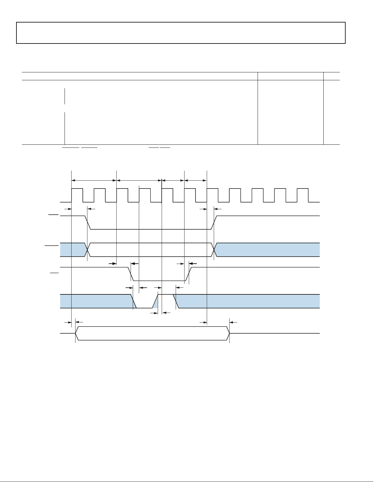
ADSP-BF534 Preliminary Technical Data
Asynchronous Memory Write Cycle Timing
Table 16. Asynchronous Memory Write Cycle Timing
Parameter Minimum Maximum Unit
Timing Requirements
t
SARDY
t
HARDY
Switching Characteristic
t
DDAT
t
ENDAT
t
DO
t
HO
1
Output pins include AMS3– 0, ABE1–0, ADDR19 –1, DATA15–0, AOE, AWE.
ARDY Setup Before CLKOUT 4.0 ns
ARDY Hold After CLKOUT 0.0 ns
DATA15– 0 Disable After CLKOUT 6.0 ns
DATA15 – 0 Enable After CLKOUT 1.0 ns
Output Delay After CLKOUT
Output Hold After CLKOUT
1
1
0.8 ns
6.0 ns
CLKOUT
AMSx
ABE1–0
ADDR19–1
AWE
ARDY
DATA15–0
SETUP
2CYCLES
t
t
ENDA T
DO
t
DO
PROGRAMMED WRITE
ACCESS 2 CYCLES
BE, ADDRESS
t
SARDY
WRITE DATA
t
SARDY
ACCESS
EXTENDED
1CYCLE
t
HO
HOLD
1CYCLE
t
HARDY
t
HO
t
DDAT
Figure 11. Asynchronous Memory Write Cycle Timing
Rev. PrD | Page 26 of 60 | January 2005

SDRAM Interface Timing
ADSP-BF534Preliminary Technical Data
Table 17. SDRAM Interface Timing (VDD
=1.2 V)
INT
Parameter Minimum Maximum Unit
Timing Requirement
t
SSDAT
t
HSDAT
DATA Setup Before CLKOUT 2.1 ns
DATA Hold After CLKOUT 0.8 ns
Switching Characteristic
t
SCLK
t
SCLKH
t
SCLKL
t
DCAD
t
HCAD
t
DSDAT
t
ENSDAT
1
The t
value is the inverse of the f
SCLK
2
Command pins include: SRAS, SCAS, SWE, SDQM, SMS, SA10, SCKE.
CLKOUT Period
CLKOUT Width High 2.5 ns
CLKOUT Width Low 2.5 ns
Command, ADDR, Data Delay After CLKOUT
Command, ADDR, Data Hold After CLKOUT
Data Disable After CLKOUT 6.0 ns
Data Enable After CLKOUT 1.0 ns
CLKOUT
DATA (IN)
1
2
2
specification discussed in Table 13. Package type and reduced supply voltages affect the best-case value of 7.5ns listed here.
SCLK
t
SCLK
t
SSDAT
t
HSDAT
t
SCLKL
7.5 ns
6.0 ns
0.8 ns
t
SCLKH
DATA(OUT)
CMND ADDR
(OUT)
t
DCAD
t
ENSDAT
t
DCAD
t
HCAD
NOTE: COMMAND = SRAS, SCAS, SWE,SDQM,SM S, SA10, SCKE.
Figure 12. SDRAM Interface Timing
t
DSDAT
t
HCAD
Rev. PrD | Page 27 of 60 | January 2005

ADSP-BF534 Preliminary Technical Data
External Port Bus Request and Grant Cycle Timing
Table 18 and Figure 13 describe external port bus request and
bus grant operations.
Table 18. External Port Bus Request and Grant Cycle Timing
Parameter
Timing Requirements
t
BS
t
BH
Switching Characteristics
t
SD
t
SE
t
DBG
t
EBG
t
DBH
t
EBH
1
These are preliminary timing parameters that are based on worst-case operating conditions.
2
The pad loads for these timing parameters are 20 pF.
1, 2
Minimum Maximum Unit
BR asserted to CLKOUT high setup 4.6 ns
CLKOUT high to BR de-asserted hold time 0.0 ns
CLKOUT low to xMS, address, and RD/WR disable 4.5 ns
CLKOUT low to xMS, address, and RD/WR enable 4.5 ns
CLKOUT high to BG asserted setup 3.6 ns
CLKOUT high to BG de-asserted hold time 3.6 ns
CLKOUT high to BGH asserted setup 3.6 ns
CLKOUT high to BGH de-asserted hold time 3.6 ns
CLKOUT
BR
AMSx
ADDR19-1
ABE1-0
AWE
ARE
BG
BGH
t
BS
t
BH
t
SD
t
SD
t
SD
t
t
DBG
DBH
t
t
EBG
EBH
t
SE
t
SE
t
SE
Figure 13. External Port Bus Request and Grant Cycle Timing
Rev. PrD | Page 28 of 60 | January 2005

ADSP-BF534Preliminary Technical Data
External DMA Request Timing
Table 19 and Figure 14 describe the External DMA Request
operations.
Table 19. External DMA Request Timing
Parameter Minimum Maximum Unit
Timing Parameters
t
DR
t
DH
Switching Characteristics
t
DO
t
HO
1
System Outputs=DATA15–0, ADDR19–1, ABE1–0 , AOE, ARE, AWE, AMS3–0, SRAS, SCAS, SWE, SCKE, CLKOUT, SA10, SMS, SCL, SDA, TSCLK0, TFS0, RFS0, RSCLK0,
DT0PRI, DT0SEC, PF15–0, PG15–0, PH15–0, RTX0, TD0, EMU
DMARx asserted to CLKOUT high setup TBD TBD ns
CLKOUT high to DMARx de-asserted hold time TBD TBD ns
Output delay after CLKOUT
Output hold after CLKOUT
CLKOUT
1
1
, XTAL, VROUT.
TBD TBD ns
TBD TBD ns
DMAR0/1
AMSx
t
DR
t
DO
t
DH
t
HO
Figure 14. External DMA Request Timing
Rev. PrD | Page 29 of 60 | January 2005

ADSP-BF534 Preliminary Technical Data
Parallel Peripheral Interface Timing
Table 20 and Figure 15 on page 30, Figure 16 on page 33, and
Figure 17 on page 34 describe Parallel Peripheral Interface
operations.
Table 20. Parallel Peripheral Interface Timing
Parameter Minimum Maximum Unit
Timing Requirements
t
PCLKW
t
PCLK
PPI_CLK Width
PPI_CLK Period
Timing Requirements - GP Input and Frame Capture Modes
t
SFSPE
t
HFSPE
t
SDRPE
t
HDRPE
External Frame Sync Setup Before PPI_CLK 3.0 ns
External Frame Sync Hold After PPI_CLK 3.0 ns
Receive Data Setup Before PPI_CLK 2.0 ns
Receive Data Hold After PPI_CLK 4.0 ns
Switching Characteristics - GP Output and Frame Capture Modes
t
DFSPE
t
HOFSPE
t
DDTPE
t
HDTPE
1
PPI_CLK frequency cannot exceed f
Internal Frame Sync Delay After PPI_CLK 10.0 ns
Internal Frame Sync Hold After PPI_CLK 0.0 ns
Transmit Data Delay After PPI_CLK 10.0 ns
Transmit Data Hold After PPI_CLK 0.0 ns
SCLK
1
1
6.0 ns
15.0 ns
/2
PPI_CLK
PPI_FS1
PPI_FS2
PPIx
t
HOFSPE
t
HDTPE
DRIVE
EDGE
t
DFSPE
t
DDTPE
t
PCLKW
t
SFSPE
t
SDRPE
SAMPLE
EDGE
Figure 15. Parallel Peripheral Interface Timing
t
HFSPE
t
HDRPE
Rev. PrD | Page 30 of 60 | January 2005

ADSP-BF534Preliminary Technical Data
Serial Ports
Table 21 through Table 26 on page 32 and Figure 16 on page 33
through Figure 18 on page 35 describe Serial Port operations.
Table 21. Serial Ports—External Clock
Parameter Minimum Maximum Unit
Timing Requirements
t
SFSE
t
HFSE
t
SDRE
t
HDRE
t
SCLKEW
t
SCLKE
1
Referenced to sample edge.
TFS/RFS Setup Before TSCLK/RSCLK
TFS/RFS Hold After TSCLK/RSCLK
Receive Data Setup Before RSCLK
Receive Data Hold After RSCLK
TSCLK/RSCLK Width 4.5 ns
TSCLK/RSCLK Period 15.0 ns
Table 22. Serial Ports—Internal Clock
Parameter Minimum Maximum Unit
Timing Requirements
t
SFSI
t
HFSI
t
SDRI
t
HDRI
t
SCLKEW
t
SCLKE
1
Referenced to sample edge.
TFS/RFS Setup Before TSCLK/RSCLK
TFS/RFS Hold After TSCLK/RSCLK
Receive Data Setup Before RSCLK
Receive Data Hold After RSCLK
TSCLK/RSCLK Width 4.5 ns
TSCLK/RSCLK Period 15.0 ns
1
1
1
1
1
1
1
1
3.0 ns
3.0 ns
3.0 ns
3.0 ns
8.0 ns
–2.0 ns
6.0 ns
0.0 ns
Table 23. Serial Ports—External Clock
Parameter Minimum Maximum Unit
Switching Characteristics
t
DFSE
t
HOFSE
t
DDTE
t
HDTE
1
Referenced to drive edge.
TFS/RFS Delay After TSCLK/RSCLK (Internally Generated TFS/RFS)
TFS/RFS Hold After TSCLK/RSCLK (Internally Generated TFS/RFS)
Transmit Data Delay After TSCLK
Transmit Data Hold After TSCLK
1
1
1
1
0.0 ns
10.0 ns
10.0 ns
0.0 ns
Table 24. Serial Ports—Internal Clock
Parameter Minimum Maximum Unit
Switching Characteristics
t
DFS
I
t
HOFS
I
t
DDT
I
t
HDT
I
t
SCLKIW
1
Referenced to drive edge.
TFS/RFS Delay After TSCLK/RSCLK (Internally Generated TFS/RFS)
TFS/RFS Hold After TSCLK/RSCLK (Internally Generated TFS/RFS)
Transmit Data Delay After TSCLK
Transmit Data Hold After TSCLK
1
1
TSCLK/RSCLK Width 4.5 ns
1
1
−1.0 ns
3.0 ns
3.0 ns
−2.0 ns
Rev. PrD | Page 31 of 60 | January 2005

ADSP-BF534 Preliminary Technical Data
Table 25. Serial Ports—Enable and Three-State
Parameter Minimum Maximum Unit
Switching Characteristics
t
DTENE
t
DDTTE
t
DTENI
t
DDTTI
1
Referenced to drive edge.
Data Enable Delay from External TSCLK
Data Disable Delay from External TSCLK
Data Enable Delay from Internal TSCLK
Data Disable Delay from Internal TSCLK
Table 26. External Late Frame Sync
Parameter Minimum Maximum Unit
Switching Characteristics
t
DDTLFSE
t
DTENL FSE
1
MCE = 1, TFS enable and TFS valid follow t
2
If external RFS/TFS setup to RSCLK/TSCLK > t
Data Delay from Late External TFS or External RFS with MCE = 1, MFD = 0
Data Enable from late FS or MCE = 1, MFD = 0
and t
DDTENFS
SCLKE
DDTLFSE
/2 then t
DDTLSCK
1
1
1
1
1,2
1,2
.
and t
apply, otherwise t
DTENLSCK
DDTLFSE
and t
DTENLFS
apply.
0.0 ns
10.0 ns
–2.0 ns
3.0 ns
10.0 ns
0.0 ns
Rev. PrD | Page 32 of 60 | January 2005

ADSP-BF534Preliminary Technical Data
DATA RECEIVE- INTERNAL CLOCK
RSCLK
TSCLK
DRIVE
EDGE
t
DFSE
t
HOFSE
RFS
DR
NOTE: EITHER THE RISING EDGE OR FALLING EDGE OF RCLK, TCLK CAN BE USED AS THE ACTIVE SAMPLING EDGE.
DATA TRANSMIT- INTERNAL CLOCK
DRIVE
EDGE
t
DFSI
t
HOFSI
TFS
t
t
HDTI
DT
DDTI
t
SCLKIW
t
SCLKIW
t
SFSI
t
SDRI
t
SFSI
SAMPLE
EDGE
SAMPLE
EDGE
t
t
HFSI
HDRI
t
HFSI
DATA RECEIVE- EXTERNAL CLOCK
DRIVE
EDGE
RSCLK
t
HOFSE
RFS
DR
DATA TRANSMIT- EXTERNAL CLOCK
DRIVE
EDGE
TSCLK
t
HOFSE
TFS
t
HDTE
DT
t
t
DFSE
DFSE
t
DDTE
t
SCLKEW
t
SCLKEW
t
SFSE
t
SDRE
t
SFSE
SAMPLE
EDGE
SAMPLE
EDGE
t
HFSE
t
HDRE
t
HFSE
TSCLK (EXT)
TFS ("LATE", EXT.)
DT
TSCLK (INT)
TFS ("LATE", INT.)
DT
NOTE: EITHER THE RISING EDGE OR FALLING EDGE OF RCLK OR TCLK CAN BE USED AS THE ACTIVE SAMPLING EDGE.
DRIVE
EDGE
DRIVE
EDGE
t
t
DDTENI
TSCLK / RSCLK
DDTENE
TSCLK / RSCLK
DRIVE
EDGE
DRIVE
EDGE
t
DDTTI
t
DDTTE
Figure 16. Serial Ports
Rev. PrD | Page 33 of 60 | January 2005

ADSP-BF534 Preliminary Technical Data
EXTERNAL RFS WITHMCE = 1, MFD = 0
DRIVE DRIVESAMPLE
RSCLK
RFS
DT
LATE EXTERNAL TFS
DRIVE DRIVESAMPLE
TSCLK
TFS
DT
t
SFSE/I
t
SFSE/I
t
DTENLFSE
t
DDTLFSE
t
DTENLFSE
t
DDTLFSE
t
HDTE/I
t
HDTE/I
t
HOFSE/I
t
DDTE/I
t
DDTE/I
t
HOFSE/I
2ND BIT1ST B IT
2ND BIT1ST B IT
Figure 17. External Late Frame Sync (Frame Sync Setup < t
SCLKE
/2)
Rev. PrD | Page 34 of 60 | January 2005

EXTERNAL RFS WITH MCE=1, MFD=0
ADSP-BF534Preliminary Technical Data
DRIVE SAMPLE
RSCLK
RFS
DT
LATE EXTERNAL TFS
DRIVE SAMPLE
TSCLK
TFS
t
SFSE/ I
t
DDTLSCK
t
SFSE/I
t
DTENLSCK
t
DTENLSCK
1ST BIT
DRIVE
DRIVE
t
HOFSE/I
t
t
HDTE/I
t
HOFSE/I
t
t
HDTE/I
DDTE/I
2ND BIT
DDTE/I
DT
1ST BIT 2ND BIT
t
DDTLSCK
Figure 18. External Late Frame Sync (Frame Sync Setup > t
SCLKE
/2)
Rev. PrD | Page 35 of 60 | January 2005

ADSP-BF534 Preliminary Technical Data
Serial Peripheral Interface (SPI) Port—Master Timing
Table 27 and Figure 19 describe SPI port master operations.
Table 27. Serial Peripheral Interface (SPI) Port—Master Timing
Parameter Minimum Maximum Unit
Timing Requirements
t
SSPIDM
t
HSPIDM
Switching Characteristics
t
SDSCIM
t
SPICHM
t
SPICLM
t
SPICLK
t
HDSM
t
SPITDM
t
DDSPIDM
t
HDSPIDM
Data input valid to SCK edge (data input setup) 7.5 ns
SCK sampling edge to data input invalid –1.5 ns
SPISELx low to first SCK edge (x=0 or 1) 2t
Serial clock high period 2t
Serial clock low period 2t
Serial clock period 4t
Last SCK edge to SPISELx high (x=0 or 1) 2t
Sequential transfer delay 2t
–1.5 ns
SCLK
–1.5 ns
SCLK
–1.5 ns
SCLK
–1.5 ns
SCLK
–1.5 ns
SCLK
–1.5 ns
SCLK
SCK edge to data out valid (data out delay) 0 6 ns
SCK edge to data out invalid (data out hold) –1.0 4.0 ns
SPISELx
(OUTPUT)
CPHA=1
CPHA=0
SCK
(CPOL = 0)
(OUTPUT)
SCK
(CPOL = 1)
(OUTPUT)
MOSI
(OUTPUT)
MISO
(INPUT)
MOSI
(OUTPUT)
MISO
(INPUT)
t
SSPIDM
t
SDSCIM
MSB VALID
t
SSPIDM
t
t
t
SPICHMtSPICLM
t
MSB VALID
t
HSPIDM
t
SPICHM
DDSPIDM
t
HSPIDM
SPICLM
t
DDSPIDM
SPICLK
t
HDSPIDM
t
SSPIDM
LSB VALID
LSB VALID
t
HDSPIDM
LSBMSB
Figure 19. Serial Peripheral Interface (SPI) Port—Master Timing
t
HDSM
LSBMSB
t
HSPIDM
t
SPITDM
Rev. PrD | Page 36 of 60 | January 2005

ADSP-BF534Preliminary Technical Data
Serial Peripheral Interface (SPI) Port—Slave Timing
Table 28 and Figure 20 describe SPI port slave operations.
Table 28. Serial Peripheral Interface (SPI) Port—Slave Timing
Parameter Minimum Maximum Unit
Timing Requirements
t
SPICHS
t
SPICLS
t
SPICLK
t
HDS
t
SPITDS
t
SDSCI
t
SSPID
t
HSPID
Switching Characteristics
t
DSOE
t
DSDHI
t
DDSPID
t
HDSPID
Serial clock high period 2t
Serial clock low period 2t
Serial clock period 4t
Last SCK edge to SPISS not asserted 2t
Sequential Transfer Delay 2t
SPISS assertion to first SCK edge 2t
–1.5 ns
SCLK
–1.5 ns
SCLK
–1.5 ns
SCLK
–1.5 ns
SCLK
–1.5 ns
SCLK
–1.5 ns
SCLK
Data input valid to SCK edge (data input setup) 1.6 ns
SCK sampling edge to data input invalid 1.6 ns
SPISS assertion to data out active 0 8 ns
SPISS deassertion to data high impedance 0 8 ns
SCK edge to data out valid (data out delay) 0 10 ns
SCK edge to data out invalid (data out hold) 0 10 ns
CPHA=1
CPHA=0
SPISS
(INPUT)
SCK
(CPOL = 0)
(INPUT)
SCK
(CPOL = 1)
(INPUT)
MISO
(OUTPUT )
MOSI
(INPUT)
MISO
(OUTPUT )
MOSI
(INPUT)
t
DSOE
t
DSOE
t
SDSCI
t
SPICHStSPICLS
t
SPICLS
t
DDSPID
t
SSPID
MSB VALID
t
MSB VALID
DDSPID
MSB
t
SPICHS
t
HDSPID
t
HSPID
t
SSPID
t
SPICL K
t
DDSPID
t
SSPID
LSB VALID
LSB VALID
LSB
t
HSPID
t
HDS
t
LSBMSB
t
DSDHI
DSDHI
t
HSPID
t
SPITDS
Figure 20. Serial Peripheral Interface (SPI) Port—Slave Timing
Rev. PrD | Page 37 of 60 | January 2005

ADSP-BF534 Preliminary Technical Data
Universal Asynchronous Receiver-Transmitter
(UART) Ports—Receive and Transmit Timing
Figure 21 describes the UART ports receive and transmit opera-
tions. The maximum baud rate is SCLK/16. As shown in
Figure 21 there is some latency between the generation of
CLKOUT
(SAMPLE CLOCK)
internal UART interrupts and the external data operations.
These latencies are negligible at the data transmission rates for
the UART.
UARTX RX
RECEIVE
UART RECEIVE
UARTX TX
TRANSMIT
UART TRANSMIT
INTERNAL
INTERRUPT
INTERNAL
INTERRUPT
DATA(5–8)
START
DATA(5–8)
Figure 21. UART Ports—Receive and Transmit Timing
STOP
STOP (1–2)
UART RECEIVE BIT SET BY DATA STOP;
CLEARED BY FIFO READ
UART TRANSMIT BIT SET BY PROGRAM;
CLEARED BY WRITE TO TRANSMIT
Rev. PrD | Page 38 of 60 | January 2005

ADSP-BF534Preliminary Technical Data
General-Purpose Port Timing
Table 29 and Figure 22 describe general-purpose port
operations.
Table 29. General-Purpose Port Timing
Parameter Minimum Maximum Unit
Timing Requirement
t
WFI
t
GPPIS
t
GPPIH
Switching Characteristic
t
GPOD
General-purpose port pin input pulsewidth t
+ 1 ns
SCLK
General-purpose port pin input setup TBD ns
General-purpose port pin input hold TBD ns
General-purpose port pin output delay from CLKOUT low 0 6 ns
CLKOUT
t
GPOD
GPP OUTPUT
GPP INPUT
t
GPPIS
t
GPPIH
t
WFI
Figure 22. General-Purpose Port Timing
Rev. PrD | Page 39 of 60 | January 2005

ADSP-BF534 Preliminary Technical Data
Timer Cycle Timing
Table 30 and Figure 23 describe timer expired operations. The
input signal is asynchronous in “width capture mode” and
“external clock mode” and has an absolute maximum input frequency of f
Table 30. Timer Cycle Timing
Parameter Minimum Maximum Unit
Timing Characteristics
t
WL
t
WH
t
TIS
t
TIH
Switching Characteristic
t
HTO
t
TOD
1
The minimum pulsewidths apply for TMRx signals in width capture and external clock modes. They also apply to the PF15 or PPI_CLK signals in PWM output mode.
2
The minimum time for t
SCLK
/2 MHz.
Timer pulsewidth input low1 (measured in SCLK cycles) 1 SCLK
Timer pulsewidth input high1 (measured in SCLK cycles) 1 SCLK
Timer input setup time before CLKOUT low TBD ns
Timer input hold time after CLKOUT low TBD ns
Timer pulsewidth output2 (measured in SCLK cycles) 1 (232–1) SCLK
Timer output update delay after CLKOUT low 0 TBD ns
is one cycle, and the maximum time for t
HTO
equals (232–1) cycles.
HTO
CLKOUT
TIMER OUTPUT
TIMER INPUT
t
TOD
t
TIS
t
TIH
Figure 23. Timer Cycle Timing
Rev. PrD | Page 40 of 60 | January 2005

ADSP-BF534Preliminary Technical Data
JTAG Test And Emulation Port Timing
Table 31 and Figure 24 describe JTAG port operations.
Table 31. JTAG Port Timing
Parameter Minimum Maximum Unit
Timing Parameters
t
TCK
t
STAP
t
HTAP
t
SSYS
t
HSYS
t
TRSTW
Switching Characteristics
t
DTDO
t
DSYS
1
System Inputs=DATA15–0, BR, ARDY, SCL, SDA, TFS0, TSCLK0, RSCLK0, RFS0, DR0PRI, DR0SEC, PF15–0, PG15–0, PH15–0, RTXI, TCK, TD1, TMS, TRST, CLKIN,
RESET, NMI, BMODE2–0.
2
50 MHz Maximum
3
System Outputs=DATA15–0, ADDR19–1, ABE1–0 , AOE, ARE, AWE, AMS3–0, SRAS, SCAS, SWE, SCKE, CLKOUT, SA10, SMS, SCL, SDA, TSCLK0, TFS0, RFS0, RSCLK0,
DT0PRI, DT0SEC, PF15–0, PG15–0, PH15–0, RTX0, TD0, EMU
TCK Period 20 ns
TDI, TMS Setup Before TCK High 4 ns
TDI, TMS Hold After TCK High 4 ns
System Inputs Setup Before TCK High
System Inputs Hold After TCK High
1
1
4ns
5ns
TRST Pulsewidth2 (measured in TCK cycles) 4 TCK
TDO Delay from TCK Low 10 ns
System Outputs Delay After TCK Low
3
, XTAL, VROUT.
012ns
TCK
TMS
TDI
TDO
SYSTEM
INPUTS
SYSTEM
OUTPUTS
t
DSYS
t
DTDO
t
SSYS
t
STAP
t
TCK
t
HTAP
t
HSYS
Figure 24. JTAG Port Timing
Rev. PrD | Page 41 of 60 | January 2005

ADSP-BF534 Preliminary Technical Data
TWI Controller Timing
Table 32 through Table 39 and Figure 25 through Figure 28
describe the TWI Controller operations.
Table 32. TWI Controller Timing: Bus Start/Stop Bits, Slave Mode, 100 kHz
Parameter Minimum Maximum Unit
t
SU:STA
t
HD:STA
t
SU:STO
t
HD:STO
Table 33. TWI Controller Timing: Bus Start/Stop Bits, Slave Mode, 400 kHz
Parameter Minimum Maximum Unit
t
SU:STA
t
HD:STA
t
SU:STO
t
HD:STO
Table 34. TWI Controller Timing: Bus Data Requirements, Slave Mode, 100 kHz
Parameter Minimum Maximum Unit
t
HIGH
t
LOW
t
R
t
F
t
SU:STA
t
HD:STA
t
HD:DAT
t
SU:DAT
t
SU:STO
t
TAA
t
BUF
C
B
1
As a transmitter, the device must provide this internal minimum delay time to bridge the undefined region (min. TBD ns) of the falling edge of SCL to avoid unintended
generation of START or STOP conditions.
2
A Fast mode TWI bus device can be used in a Standard mode TWI bus system, but the requirement T
the device does not stretch the LOW period of the SCL signal. If such a device does stretch the LOW period of the SCL signal, it must output the next data bit to the SDA
line. Before the SCL line is released, T
Start condition setup time TBD - ns
Start condition hold time TBD - ns
Stop condition setup time TBD - ns
Stop condition hold time TBD - ns
Start condition setup time TBD - ns
Start condition hold time TBD - ns
Stop condition setup time TBD - ns
Stop condition hold time TBD - ns
Clock high time TBD - µs
Clock low time TBD - µs
SDA and SCL rise time - TBD ns
SDA and SCL fall time - TBD ns
Start condition setup time TBD - µs
Start condition hold time TBD - µs
Data input hold time TBD - ns
Data input setup time
1
TBD - ns
Stop condition setup time TBD - µs
Output valid from clock
2
-TBDns
Bus free time TBD - µs
Bus capacitive loading - TBD pF
>= 250 ns must then be met. This will automatically be the case if
SU:DAT
max. + T
R
= 1000 + 250 = 1250 ns (according to the Standard mode I2C bus specification).
SU:DAT
Rev. PrD | Page 42 of 60 | January 2005

ADSP-BF534Preliminary Technical Data
Table 35. TWI Controller Timing: Bus Data Requirements, Slave Mode, 400 kHz
Parameter Minimum Maximum Unit
t
HIGH
t
LOW
t
R
t
F
t
SU:STA
t
HD:STA
t
HD:DAT
t
SU:DAT
t
SU:STO
t
TAA
t
BUF
C
B
1
As a transmitter, the device must provide this internal minimum delay time to bridge the undefined region (min. TBD ns) of the falling edge of SCL to avoid unintended
generation of START or STOP conditions.
Table 36. TWI Controller Timing: Bus Start/Stop Bits, Master Mode, 100 kHz
Parameter Minimum Maximum Unit
t
SU:STA
t
HD:STA
t
SU:STO
t
HD:STO
Clock high time TBD - µs
Clock low time TBD - µs
SDA and SCL rise time TBD TBD ns
SDA and SCL fall time TBD TBD ns
Start condition setup time TBD - µs
Start condition hold time TBD - µs
Data input hold time TBD TBD µs
Data input setup time
1
TBD - ns
Stop condition setup time TBD - µs
Output valid from clock - - ns
Bus free time TBD - µs
Bus capacitive loading - TBD pF
Start condition setup time TBD - ns
Start condition hold time TBD - ns
Stop condition setup time TBD - ns
Stop condition hold time TBD - ns
Table 37. TWI Controller Timing: Bus Start/Stop Bits, Master Mode, 400 kHz
Parameter Minimum Maximum Unit
t
SU:STA
t
HD:STA
t
SU:STO
t
HD:STO
Start condition setup time TBD - ns
Start condition hold time TBD - ns
Stop condition setup time TBD - ns
Stop condition hold time TBD - ns
Table 38. TWI Controller Timing: Bus Data Requirements, Master Mode, 100 kHz
Parameter Minimum Maximum Unit
t
HIGH
t
LOW
t
R
t
F
t
SU:STA
t
HD:STA
t
HD:DAT
t
SU:DAT
t
SU:STO
t
TAA
t
BUF
C
B
1
A Fast mode TWI bus device can be used in a Standard mode TWI bus system, but the requirement T
the device does not stretch the LOW period of the SCL signal. If such a device does stretch the LOW period of the SCL signal, it must output the next data bit to the SDA
line. Before the SCL line is released, T
Clock high time TBD - ms
Clock low time TBD - ms
SDA and SCL rise time - TBD ns
SDA and SCL fall time - TBD ns
Start condition setup time TBD - ms
Start condition hold time TBD - ms
Data input hold time TBD - ns
Data input setup time
1
TBD - ns
Stop condition setup time TBD - ms
Output valid from clock - TBD ns
Bus free time TBD - ms
Bus capacitive loading - TBD pF
>= 250 ns must then be met. This will automatically be the case if
SU:DAT
max. + T
R
= 1000 + 250 = 1250 ns (according to the Standard mode I2C bus specification).
SU:DAT
Rev. PrD | Page 43 of 60 | January 2005

ADSP-BF534 Preliminary Technical Data
Table 39. TWI Controller Timing: Bus Data Requirements, Master Mode, 400 kHz
Parameter Minimum Maximum Unit
t
HIGH
t
LOW
t
R
t
F
t
SU:STA
t
HD:STA
t
HD:DAT
t
SU:DAT
t
SU:STO
t
TAA
t
BUF
C
B
1
A Fast mode TWI bus device can be used in a Standard mode TWI bus system, but the requirement T
the device does not stretch the LOW period of the SCL signal. If such a device does stretch the LOW period of the SCL signal, it must output the next data bit to the SDA
line. Before the SCL line is released, T
Clock high time TBD - ms
Clock low time TBD - ms
SDA and SCL rise time TBD TBD ns
SDA and SCL fall time TBD TBD ns
Start condition setup time TBD - ms
Start condition hold time TBD - ms
Data input hold time TBD TBD ns
Data input setup time
1
TBD - ns
Stop condition setup time TBD - ms
Output valid from clock - - ns
Bus free time TBD - ms
Bus capacitive loading - TBD pF
>= 250 ns must then be met. This will automatically be the case if
SU:DAT
max. + T
R
= 1000 + 250 = 1250 ns (according to the Standard mode I2C bus specification).
SU:DAT
SCL
SDA
(I N)
SDA
(OUT)
SCL
SDA
t
SU:S TA
t
SU:STA
HD:STA
START
t
SU:STO
STOP
t
Figure 25. TWI Controller Timing: Bus Start/Stop Bits, Slave Mode
t
F
t
HD:STA
t
AA
t
HIGH
t
HD:DAT
t
LO W
t
SU:DAT
t
AA
t
t
Figure 26. TWI Controller Timing: Bus Data, Slave Mode
R
SU:STO
t
HD:STO
t
BUF
Rev. PrD | Page 44 of 60 | January 2005

SCL
SDA
t
SU:STA
t
HD:STA
t
SU:STO
t
HD:STO
ADSP-BF534Preliminary Technical Data
SCL
SDA
(I N)
SDA
(OUT)
t
SU:S TA
START
STOP
Figure 27. TWI Controller Timing: Bus Start/Stop Bits, Master Mode
t
F
t
HD:STA
t
AA
t
HIGH
t
HD:DAT
t
LO W
t
SU:DAT
t
AA
t
R
t
SU:STO
Figure 28. TWI Controller Timing: Bus Data, Master Mode
t
BUF
Rev. PrD | Page 45 of 60 | January 2005

ADSP-BF534 Preliminary Technical Data
OUTPUT DRIVE CURRENTS
Figure 29 through Figure 38 show typical current-voltage char-
acteristics for the output drivers of the ADSP-BF534 processor.
The curves represent the current drive capability of the output
drivers as a function of output voltage. See Table 9 on page 17
for information about which driver type corresponds to a particular pin.
150
100
50
0
TBD
150
100
–50
SOURCE CURRENT (mA)
–100
–50
SOURCE CURRENT (mA)
–100
–150
150
100
–50
SOURCE CURRENT (mA)
–100
50
0
TBD
0
0.5 1.0 1.5 2.0 2.5 3.0
SOURCE VOLTAGE (V)
Figure 29. Drive Current A (Low V
DDEXT
)
–150
150
100
0
50
0
0.5 1.0 1.5 2.0 2.5 3.0
SOURCE VOLTAGE (V)
Figure 31. Drive Current B (Low V
DDEXT
)
TBD
–50
SOURCE CURRENT (mA)
–100
50
0
TBD
–150
0
0.5 1.0 1.5 2.0 2.5 3.0
Figure 32. Drive Current B (High V
SOURCE VOLTAGE (V)
DDEXT
)
–150
0
0.5 1.0 1.5 2.0 2.5 3.0
Figure 30. Drive Current A (High V
SOURCE VOLTAGE (V)
)
DDEXT
Rev. PrD | Page 46 of 60 | January 2005

ADSP-BF534Preliminary Technical Data
150
100
–50
SOURCE CURRENT (mA)
–100
–150
150
100
150
100
50
0
TBD
0
50
0.5 1.0 1.5 2.0 2.5 3.0
SOURCE VOLTAGE (V)
Figure 33. Drive Current C (Low V
DDEXT
)
–50
SOURCE CURRENT (mA)
–100
–150
150
100
50
0
TBD
0
50
0.5 1.0 1.5 2.0 2.5 3.0
SOURCE VOLTAGE (V)
Figure 35. Drive Current D (Low V
DDEXT
)
–50
SOURCE CURRENT (mA)
–100
–150
0
TBD
0
0.5 1.0 1.5 2.0 2.5 3.0
SOURCE VOLTAGE (V)
Figure 34. Drive Current C (High V
DDEXT
)
–50
SOURCE CURRENT (mA)
–100
–150
0
TBD
0
0.5 1.0 1.5 2.0 2.5 3.0
Figure 36. Drive Current D (High V
SOURCE VOLTAGE (V)
DDEXT
)
Rev. PrD | Page 47 of 60 | January 2005

ADSP-BF534 Preliminary Technical Data
150
100
50
0
TBD
–50
SOURCE CURRENT (mA)
–100
–150
0
0.5 1.0 1.5 2.0 2.5 3.0
SOURCE VOLTAGE (V)
150
100
–50
SOURCE CURRENT (mA)
–100
–150
Figure 37. Drive Current E (Low V
50
0
DDEXT
)
TBD
0
0.5 1.0 1.5 2.0 2.5 3.0
SOURCE VOLTAGE (V)
Figure 38. Drive Current E (High V
DDEXT
)
Rev. PrD | Page 48 of 60 | January 2005

ADSP-BF534Preliminary Technical Data
POWER DISSIPATION
Total power dissipation has two components: one due to internal circuitry (P
output drivers (P
internal circuitry (V
dent on the instruction execution sequence and the data
operands involved.
The external component of total power dissipation is caused by
the switching of output pins. Its magnitude depends on:
• Maximum frequency (f
switch during each cycle
• Load capacitance (C
• Their voltage swing (V
The external component is calculated using:
Table 40. Internal Power Dissipation
Parameter f
2
I
DDTYP
3
I
DDEFR
45
I
DDSLEEP
I
DDDEEPSLEEP
I
DDHIBERNATE
Parameter f
2
I
DDTYP
3
I
DDEFR
45
I
DDSLEEP
I
DDDEEPSLEEP
I
DDHIBERNATE
1
IDD data is specified for typical process parameters. All data at 25ºC.
2
Processor executing 75% dual Mac, 25% ADD with moderate data bus activity.
3
Implementation of Enhanced Full Rate (EFR) GSM algorithm.
4
See the ADSP-BF534 Blackfin Processor Hardware Reference Manual for defini-
tions of Sleep and Deep Sleep operating modes.
5
I
DDHIBERNATE
) and one due to the switching of external
INT
). Table 40 shows the power dissipation for
EXT
). Internal power dissipation is depen-
DDINT
) at which all output pins can
0
) of all switching output pins
0
)
DDEXT
P
EXT
V
DDEXT
2
C0f0⋅
×=
∑
Test Conditions1
=
CCLK
50 MHz
V
=
DDINT
0.8 V
=
f
CCLK
150 MHz
V
=
DDINT
0.9 V
=
f
CCLK
250 MHz
V
=
DDINT
1.0 V
=
f
CCLK
400 MHz
V
=
DDINT
1.2 V
TBDTBDTBDTBDmA
TBDTBDTBDTBDmA
TBDTBDTBDTBDmA
4
TBDTBDTBDTBDmA
5
50 50 50 50 µA
=
CCLK
200 MHz
=
V
DDINT
0.9 V
f
CCLK
400 MHz
V
DDINT
1.0 V
=
=
f
=
CCLK
500 MHz
=
V
DDINT
1.2 V
- TBD TBD TBD mA
- TBD TBD TBD mA
- TBD TBD TBD mA
4
- TBD TBD TBD mA
5
-505050µA
is measured @ V
= 3.65 V with VR off (V
DDEXT
DDCORE
=0V).
Unit
Unit
The frequency f includes driving the load high and then back
low. For example: DATA15–0 pins can drive high and low at a
maximum rate of 1/(2ⴛ t
) while in SDRAM burst mode.
SCLK
A typical power consumption can now be calculated for these
conditions by adding a typical internal power dissipation:
P
TOTALPEXTIDDVDDINT
Note that the conditions causing a worst-case P
those causing a worst-case P
. Maximum P
INT
×()+=
INT
differ from
EXT
cannot occur
while 100% of the output pins are switching from all ones (1s) to
all zeros (0s). Note, as well, that it is not common for an application to have 100% or even 50% of the outputs switching
simultaneously.
TEST CONDITIONS
All timing parameters appearing in this data sheet were measured under the conditions described in this section.
Output Enable Time
Output pins are considered to be enabled when they have made
a transition from a high impedance state to the point when they
start driving. The output enable time t
the point when a reference signal reaches a high or low voltage
level to the point when the output starts driving as shown in the
Output Enable/Disable diagram (Figure 39). The time
t
ENA_MEASURED
is the interval from when the reference signal
switches to when the output voltage reaches 2.0 V (output high)
or 1.0 V (output low). Time t
is the interval from when the
TRIP
output starts driving to when the output reaches the 1.0 V or
2.0 V trip voltage. Time t
is calculated as shown in the
ENA
equation:
t
ENAtENA_MEASUREDtTRIP
If multiple pins (such as the data bus) are enabled, the measurement value is that of the first pin to start driving.
is the interval from
ENA
–=
Rev. PrD | Page 49 of 60 | January 2005

ADSP-BF534 Preliminary Technical Data
Output Disable Time
Output pins are considered to be disabled when they stop driving, go into a high impedance state, and start to decay from their
output high or low voltage. The time for the voltage on the bus
to decay by ∆V is dependent on the capacitive load, C
load current, I
. This decay time can be approximated by the
L
and the
L
equation:
t
DECAY
The output disable time t
t
DIS_MEASURED
t
DIS_MEASURED
and t
is the interval from when the reference signal
as shown in Figure 39. The time
DECAY
CLV∆()IL⁄=
is the difference between
DIS
switches to when the output voltage decays ∆V from the measured output high or output low voltage. The time t
calculated with test loads C
REFERENCE
t
t
DIS
V
OH
(MEASURED)
V
OL
(MEASURED)
VOH(MEASURED) ⴚ⌬V
and IL, and with ∆V equal to 0.5 V.
L
SIGNAL
DIS_MEASURED
VOL(MEASURED) + ⌬V
t
DECAY
t
ENA
t
ENA-MEASURED
2.0V
1.0V
t
DECAY
V
OH
(MEASURED)
V
OL
(MEASURED)
TRIP
is
Example System Hold Time Calculation
To determine the data output hold time in a particular system,
first calculate t
using the equation given above. Choose ∆V
DECAY
to be the difference between the ADSP-BF534 processor’s output voltage and the input threshold for the device requiring the
hold time. A typical ∆V will be 0.4 V. C
tance (per data line), and I
is the total leakage or three-state
L
current (per data line). The hold time will be t
minimum disable time (for example, t
is the total bus capaci-
L
plus the
DECAY
for an SDRAM write
DSDAT
cycle).
TO
OUTPUT
PIN
30pF
Figure 40. Equivalent Device Loading for AC Measurements
(Includes All Fixtures)
INPUT
1.5V 1.5V
OR
OUTPUT
Figure 41. Voltage Reference Levels for AC
Measurements (Except Output Enable/Disable)
50⍀
1.5V
OUTPUT STOPS DRIVING
VOLTAGE TO BE APPROXIMATELY 1.5V.
Figure 39. Output Enable/Disable
OUTPUT STARTS DRIVING
HIGH IMPEDANCE STATE.
TEST CONDITIONS CAUSE THIS
Rev. PrD | Page 50 of 60 | January 2005

ENVIRONMENTAL CONDITIONS
To determine the junction temperature on the application
printed circuit board use:
ADSP-BF534Preliminary Technical Data
TJT
CASEΨJTPD
×()+=
where:
T
= Junction temperature (ⴗC)
J
= Case temperature (ⴗC) measured by customer at top
T
CASE
center of package.
= From Table 41
Ψ
JT
= Power dissipation (see Power Dissipation on page 49 for
P
D
the method to calculate P
Values of θ
are provided for package comparison and printed
JA
circuit board design considerations. θ
order approximation of T
)
D
by the equation:
J
TJT
can be used for a first
JA
θ
A
×()+=
JAPD
where:
T
= Ambient temperature (ⴗC)
A
Values of θ
are provided for package comparison and printed
JC
circuit board design considerations when an external heatsink is
required.
Values of θ
are provided for package comparison and printed
JB
circuit board design considerations.
In Table 41, airflow measurements comply with JEDEC standards JESD51-2 and JESD51-6, and the junction-to-board
measurement complies with JESD51-8. The junction-to-case
measurement complies with MIL-STD-883 (Method 1012.1).
All measurements use a 2S2P JEDEC test board.
Table 41. Thermal Characteristics
Parameter Condition Typical Unit
θ
JA
θ
JMA
θ
JMA
θ
JB
θ
JC
Ψ
JT
0 linear m/s air flow ⴗC/W
1 linear m/s air flow ⴗC/W
2 linear m/s air flow ⴗC/W
ⴗC/W
ⴗC/W
0 linear m/s air flow ⴗC/W
Rev. PrD | Page 51 of 60 | January 2005

ADSP-BF534 Preliminary Technical Data
182-BALL MINI-BGA PINOUT
Table 42 lists the mini-BGA pinout by signal mnemonic.
Table 43 on page 53 lists the mini-BGA pinout by ball number.
Table 42. 182-Ball Mini-BGA Ball Assignment (Alphabetically by Signal Mnemonic)
Mnemonic Ball no. Mnemonic Ball no. Mnemonic Ball no. Mnemonic Ball no. Mnemonic Ball no.
ABE0
ABE1
ADDR1 J14 DATA1 N9 GND L10 PH0 C2 TCK P2
ADDR10 M13 DATA10 N6 GND M4 PH1 C3 TDI M3
ADDR11 M14 DATA11 P6 GND M10 PH10 B6 TDO N3
ADDR12 N14 DATA12 M5 GND P14 PH11 A2 TMS N2
ADDR13 N13 DATA13 N5 NMI
ADDR14 N12 DATA14 P5 PF0 M1 PH13 A4 VDDEXT A1
ADDR15 M11 DATA15 P4 PF1 L1 PH14 A5 VDDEXT C12
ADDR16 N11 DATA2 P9 PF10 J2 PH15 A6 VDDEXT E6
ADDR17 P13 DATA3 M8 PF11 J3 PH2 C4 VDDEXT E11
ADDR18 P12 DATA4 N8 PF12 H1 PH3 C5 VDDEXT F4
ADDR19 P11 DATA5 P8 PF13 H2 PH4 C6 VDDEXT F12
ADDR2 K14 DATA6 M7 PF14 H3 PH5 B1 VDDEXT H5
ADDR3 L14 DATA7 N7 PF15 H4 PH6 B2 VDDEXT H10
ADDR4 J13 DATA8 P7 PF2 L2 PH7 B3 VDDEXT J11
ADDR5 K13 DATA9 M6 PF3 L3 PH8 B4 VDDEXT J12
ADDR6 L13 EMU
ADDR7 K12 GND A10 PF5 K1 PJ0 C7 VDDEXT K9
ADDR8 L12 GND A14 PF6 K2 PJ1 B7 VDDEXT L7
ADDR9 M12 GND D4 PF7 K3 PJ10 D10 VDDEXT L9
AMS0
AMS1
AMS2
AMS3
AOE
ARDY E13 GND F11 PG11 D2 PJ6 C8 VDDINT G10
ARE
AWE
BG
BGH
BMODE0 N4 GND J4 PG2 G3 RTXO A8 VROUT0 A13
BMODE1 P3 GND J5 PG3 F1 RTXI A9 VROUT1 B12
BMODE2 L5 GND J9 PG4 F2 SA10 E12 XTAL A11
BR
CLKBUF A7 GND K6 PG6 E1 SCKE B13
CLKIN A12 GND K11 PG7 E2 SMS C13
H13 CLKOUT B14 GND L6 PG8 E3 SRAS D13
H12 DATA0 M9 GND L8 PG9 E4 SWE D12
B10 PH12 A3 TRST N1
M2 PF4 L4 PH9 B5 VDDEXT K7
E14 GND E7 PF8 K4 PJ11 D11 VDDEXT L11
F14 GND E9 PF9 J1 PJ2 B11 VDDEXT P1
F13 GND F5 PG0 G1 PJ3 C11 VDDINT E5
G12 GND F6 PG1 G2 PJ4 D7 VDDINT E8
G13 GND F10 PG10 D1 PJ5 D8 VDDINT E10
G14 GND G4 PG12 D3 PJ7 B8 VDDINT K5
H14 GND G5 PG13 D5 PJ8 D9 VDDINT K8
P10 GND G11 PG14 D6 PJ9 C9 VDDINT K10
N10 GND H11 PG15 C1 RESET C10 VDDRTC B9
D14 GND J10 PG5 F3 SCAS C14
Rev. PrD | Page 52 of 60 | January 2005

ADSP-BF534Preliminary Technical Data
Table 43 lists the mini-BGA pinout by ball number. Table 42 on
page 52 lists the mini-BGA pinout by signal mnemonic.
Table 43. 182-Ball Mini-BGA Ball Assignment (Numerically by Ball Number)
Ball no. Mnemonic Ball no. Mnemonic Ball no. Mnemonic Ball no. Mnemonic Ball no. Mnemonic
A1 VDDEXT C10 RESET
A2 PH11 C11 PJ3 F6 GND K1 PF5 M10 GND
A3 PH12 C12 VDDEXT F10 GND K2 PF6 M11 ADDR15
A4 PH13 C13 SMS
A5 PH14 C14 SCAS
A6 PH15 D1 PG10 F13 AMS2
A7 CLKBUF D2 PG11 F14 AMS1
A8 RTXO D3 PG12 G1 PG0 K7 VDDEXT N2 TMS
A9 RTXI D4 GND G2 PG1 K8 VDDINT N3 TDO
A10 GND D5 PG13 G3 PG2 K9 VDDEXT N4 BMODE0
A11 XTAL D6 PG14 G4 GND K10 VDDINT N5 DATA13
A12 CLKIN D7 PJ4 G5 GND K11 GND N6 DATA10
A13 VROUT0 D8 PJ5 G10 VDDINT K12 ADDR7 N7 DATA7
A14 GND D9 PJ8 G11 GND K13 ADDR5 N8 DATA4
B1 PH5 D10 PJ10 G12 AMS3
B2 PH6 D11 PJ11 G13 AOE
B3 PH7 D12 SWE G14 ARE L2 PF2 N11 ADDR16
B4 PH8 D13 SRAS
B5 PH9 D14 BR
B6 PH10 E1 PG6 H3 PF14 L5 BMODE2 N14 ADDR12
B7 PJ1 E2 PG7 H4 PF15 L6 GND P1 VDDEXT
B8 PJ7 E3 PG8 H5 VDDEXT L7 VDDEXT P2 TCK
B9 VDDRTC E4 PG9 H10 VDDEXT L8 GND P3 BMODE1
B10 NMI
B11 PJ2 E6 VDDEXT H12 ABE1
B12 VROUT1 E7 GND H13 ABE0
B13 SCKE E8 VDDINT H14 AWE
B14 CLKOUT E9 GND J1 PF9 L13 ADDR6 P8 DATA5
C1 PG15 E10 VDDINT J2 PF10 L14 ADDR3 P9 DATA2
C2 PH0 E11 VDDEXT J3 PF11 M1 PF0 P10 BG
C3 PH1 E12 SA10 J4 GND M2 EMU P11 ADDR19
C4 PH2 E13 ARDY J5 GND M3 TDI P12 ADDR18
C5 PH3 E14 AMS0
C6 PH4 F1 PG3 J10 GND M5 DATA12 P14 GND
C7 PJ0 F2 PG4 J11 VDDEXT M6 DATA9
C8 PJ6 F3 PG5 J12 VDDEXT M7 DATA6
C9 PJ 9 F 4 V D DE XT J 13 A DD R4 M8 DATA 3
E5 VDDINT H11 GND L9 VDDEXT P4 DATA15
F5 GND J14 ADDR1 M9 DATA0
F11 GND K3 PF7 M12 ADDR9
F12 VDDEXT K4 PF8 M13 ADDR10
K5 VDDINT M14 ADDR11
K6 GND N1 TRST
K14 ADDR2 N9 DATA1
L1 PF1 N10 BGH
H1 PF12 L3 PF3 N12 ADDR14
H2 PF13 L4 PF4 N13 ADDR13
L10 GND P5 DATA14
L11 VDDEXT P6 DATA11
L12 ADDR8 P7 DATA8
J9 GND M4 GND P13 ADDR17
Rev. PrD | Page 53 of 60 | January 2005

ADSP-BF534 Preliminary Technical Data
Figure 42 shows the top view of the mini-BGA ball configura-
tion. Figure 43 shows the bottom view of the mini-BGA ball
configuration.
1234567891011121314
A
B
C
D
E
F
G
H
J
K
L
M
N
P
KEY:
V
V
DDINT
DDEXT
GND
I/O
V
DDRTC
V
ROUT
NC
Figure 42. 182-Ball Mini-BGA Ball Configuration (Top View)
1234567891011121314
A
B
C
D
E
F
G
H
J
K
L
M
N
P
KEY:
V
V
DDINT
DDEXT
GND
I/O
V
V
DDRTC
ROUT
NC
Figure 43. 182-Ball Mini-BGA Ball Configuration (Bottom View)
Rev. PrD | Page 54 of 60 | January 2005
ADSP-BF534Preliminary Technical Data
208-BALL SPARSE MINI-BGA PINOUT
Table 44 lists the sparse mini-BGA pinout by signal mnemonic.
Table 45 on page 56 lists the sparse mini-BGA pinout by ball
number.
Table 44. 208-Ball Sparse Mini-BGA Ball Assignment (Alphabetically by Signal Mnemonic)
Mnemonic Ball no. Mnemonic Ball no. Mnemonic Ball no. Mnemonic Ball no. Mnemonic Ball no.
ABE0
ABE1
ADDR1 R19 DATA14 Y3 GND N11 PG8 D2 TMS U2
ADDR10 W18 DATA15 W3 GND N12 PG9 C1 TRST
ADDR11 Y18 DATA2 Y9 GND N13 PH0 B4 VDDEXT G7
ADDR12 W17 DATA3 W9 GND P11 PH1 A5 VDDEXT G8
ADDR13 Y17 DATA4 Y8 GND V2 PH10 B9 VDDEXT G9
ADDR14 W16 DATA5 W8 GND Y1 PH11 A10 VDDEXT G10
ADDR15 Y16 DATA6 Y7 GND Y20 PH12 B10 VDDEXT H7
ADDR16 W15 DATA7 W7 NC B2 PH13 A11 VDDEXT H8
ADDR17 Y15 DATA8 Y6 NC W2 PH14 B11 VDDEXT J7
ADDR18 W14 DATA9 W6 NC W19 PH15 A12 VDDEXT J8
ADDR19 Y14 EMU
ADDR2 T20 GND A1 NMI
ADDR3 T19 GND A13 PF0 T2 PH4 B6 VDDEXT L7
ADDR4 U20 GND A20 PF1 R1 PH5 A7 VDDEXT L8
ADDR5 U19 GND G11 PF10 L2 PH6 B7 VDDEXT M7
ADDR6 V20 GND H9 PF11 K1 PH7 A8 VDDEXT M8
ADDR7 V19 GND H10 PF12 K2 PH8 B8 VDDEXT N7
ADDR8 W20 GND H11 PF13 J1 PH9 A9 VDDEXT N8
ADDR9 Y19 GND H12 PF14 J2 PJ0 B12 VDDEXT P7
AMS0
AMS1
AMS2
AMS3
AOE
ARDY J19 GND J13 PF6 N2 PJ4 B18 VDDINT G14
ARE
AWE
BG
BGH
BMODE0 W13 GND K13 PG1 G1 PJ9 B20 VDDINT M14
BMODE1 W12 GND L9 PG10 C2 RESET
BMODE2 W11 GND L10 PG11 B1 RTXO A15 VDDINT P12
BR
CLKBUF B14 GND L12 PG13 A3 SA10 L20 VDDINT P14
CLKIN A18 GND L13 PG14 B3 SCAS
CLKOUT H19 GND M9 PG15 A4 SCKE H20 VROUT0 E20
DATA0 Y10 GND M10 PG2 G2 SMS
DATA1 W10 GND M11 PG3 F1 SRAS
DATA10 Y5 GND M12 PG4 F2 SWE
DATA11 W5 GND M13 PG5 E1 TCK W1
P19 DATA12 Y4 GND N9 PG6 E2 TDI V1
P20 DATA13 W4 GND N10 PG7 D1 TDO Y2
U1
T1 NC Y13 PH2 B5 VDDEXT K7
C20 PH3 A6 VDDEXT K8
M20 GND H13 PF15 H1 PJ1 B13 VDDEXT P8
M19 GND J9 PF2 R2 PJ10 B19 VDDEXT P9
G20 GND J10 PF3 P1 PJ11 C19 VDDEXT P10
G19 GND J11 PF4 P2 PJ2 D19 VDDINT G12
N20 GND J12 PF5 N1 PJ3 E19 VDDINT G13
N19 GND K9 PF7 M1 PJ5 A19 VDDINT H14
R20 GND K10 PF8 M2 PJ6 B15 VDDINT J14
Y11GNDK11PF9L1 PJ7 B16VDDINTK14
Y12GNDK12PG0H2 PJ8 B17VDDINTL14
D20 VDDINT N14
F19 GND L11 PG12 A2 RTXI A14 VDDINT P13
K20 VDDRTC A16
J20 VROUT1 F20
K19 XTAL A17
L19
Rev. PrD | Page 55 of 60 | January 2005

ADSP-BF534 Preliminary Technical Data
Table 45 lists the sparse mini-BGA pinout by ball number.
Table 44 on page 55 lists the sparse mini-BGA pinout by signal
mnemonic.
Table 45. 208-Ball Sparse Mini-BGA Ball Assignment (Numerically by Ball Number)
Ball no. Mnemonic Ball no. Mnemonic Ball no. Mnemonic Ball no. Mnemonic Ball no. Mnemonic
A1 GND C19 PJ11 J9 GND M19 AMS1
A2 PG12 C20 NMI
A3 PG13 D1 PG7 J11 GND N1 PF5 W3 DATA15
A4 PG15 D2 PG8 J12 GND N2 PF6 W4 DATA13
A5 PH1 D19 PJ2 J13 GND N7 VDDEXT W5 DATA11
A6 PH3 D20 RESET
A7 PH5 E1 PG5 J19 ARDY N9 GND W7 DATA7
A8 PH7 E2 PG6 J20 SMS
A9 PH9 E19 PJ3 K1 PF11 N11 GND W9 DATA3
A10 PH11 E20 VROUT0 K2 PF12 N12 GND W10 DATA1
A11 PH13 F1 PG3 K7 VDDEXT N13 GND W11 BMODE2
A12 PH15 F2 PG4 K8 VDDEXT N14 VDDINT W12 BMODE1
A13 GND F19 BR
A14 RTXI F20 VROUT1 K10 GND N20 AOE
A15 RTXO G1 PG1 K11 GND P1 PF3 W15 ADDR16
A16 VDDRTC G2 PG2 K12 GND P2 PF4 W16 ADDR14
A17 XTAL G7 VDDEXT K13 GND P7 VDDEXT W17 ADDR12
A18 CLKIN G8 VDDEXT K14 VDDINT P8 VDDEXT W18 ADDR10
A19 PJ5 G9 VDDEXT K19 SRAS
A20 GND G10 VDDEXT K20 SCAS
B1 PG11 G11 GND L1 PF9 P11 GND Y1 GND
B2 NC G12 VDDINT L2 PF10 P12 VDDINT Y2 TDO
B3 PG14 G13 VDDINT L7 VDDEXT P13 VDDINT Y3 DATA14
B4 PH0 G14 VDDINT L8 VDDEXT P14 VDDINT Y4 DATA12
B5 PH2 G19 AMS3
B6 PH4 G20 AMS2
B7 PH6 H1 PF15 L11 GND R1 PF1 Y7 DATA6
B8 PH8 H2 PG0 L12 GND R2 PF2 Y8 DATA4
B9 PH10 H7 VDDEXT L13 GND R19 ADDR1 Y9 DATA2
B10 PH12 H8 VDDEXT L14 VDDINT R20 AWE
B11 PH14 H9 GND L19 SWE
B12 PJ0 H10 GND L20 SA10 T2 PF0 Y12 BGH
B13 PJ1 H11 GND M1 PF7 T19 ADDR3 Y13 NC
B14 CLKBUF H12 GND M2 PF8 T20 ADDR2 Y14 ADDR19
B15 PJ6 H13 GND M7 VDDEXT U1 T
B16 PJ7 H14 VDDINT M8 VDDEXT U2 TMS Y16 ADDR15
B17 PJ8 H19 CLKOUT M9 GND U19 ADDR5 Y17 ADDR13
B18 PJ4 H20 SCKE M10 GND U20 ADDR4 Y18 ADDR11
B19PJ10J1 PF13M11GNDV1 TDI Y19ADDR9
B20 PJ9 J2 PF14 M12 GND V2 GND Y20 GND
C1 PG9 J7 VDDEXT M13 GND V19 ADDR7
C2 PG10 J8 VDDEXT M14 VDDINT V20 ADDR6
J10 GND M20 AMS0 W2 NC
J14 VDDINT N8 VDDEXT W6 DATA9
N10 GND W8 DATA5
K9 GND N19 ARE W13 BMODE0
P9 VDDEXT W19 NC
P10 VDDEXT W20 ADDR8
L9 GND P19 ABE0 Y5 DATA10
L10 GND P20 ABE1 Y6 DATA8
T1 EMU Y11 BG
RST Y15 ADDR17
W1 TCK
W14 ADDR18
Y10 DATA0
Rev. PrD | Page 56 of 60 | January 2005

Figure 44 shows the top view of the sparse mini-BGA ball con-
figuration. Figure 45 shows the bottom view of the sparse miniBGA ball configuration.
1234567891011121314 161718192015
ADSP-BF534Preliminary Technical Data
A
B
C
D
E
F
G
H
J
K
L
M
N
P
R
T
U
V
W
Y
KEY:
V
DDINT
V
DDEXT
GND
I/O
V
DDRTC
V
ROUT
NC
Figure 44. 208-Ball Mini-BGA Ball Configuration (Top View)
20 19 18 17 16 15 14 13 12 11 10 9 8 7 5 4 3 2 16
KEY:
V
V
DDINT
DDEXT
GND
I/O
V
DDRTC
V
ROUT
NC
Figure 45. 208-Ball Mini-BGA Ball Configuration (Bottom View)
A
B
C
D
E
F
G
H
J
K
L
M
N
P
R
T
U
V
W
Y
Rev. PrD | Page 57 of 60 | January 2005

ADSP-BF534 Preliminary Technical Data
OUTLINE DIMENSIONS
Dimensions in Figure 46—182-Ball Mini-BGA and Figure 47—
208-Ball Sparse Mini-BGA are shown in millimeters.
Figure 46. 182-Ball Mini-BGA
Rev. PrD | Page 58 of 60 | January 2005

ADSP-BF534Preliminary Technical Data
Figure 47. 208-Ball Sparse Mini-BGA
Rev. PrD | Page 59 of 60 | January 2005

ADSP-BF534 Preliminary Technical Data
ORDERING GUIDE
Part numbers that include “BC1” are 182-Ball mini-BGA. Part numbers that include “BC2” are 208-Ball Sparse mini-BGA. Part numbers
that include “Z” are lead free. See Figure 8 on page 22 for more information about product information on the package.
Part Number Temperature Range (Ambient) Speed Grade (Max) Operating Voltage
ADSP-BF534SBBC1400 –40ºC to 85ºC 400 MHz 1.2 V internal, 2.5 V or 3.3 V I/O
ADSPBF534SBBC1Z400 –40ºC to 85ºC 400 MHz 1.2 V internal, 2.5 V or 3.3 V I/O
ADSPBF534SBBC2Z400 –40ºC to 85ºC 400 MHz 1.2 V internal, 2.5 V or 3.3 V I/O
ADSP-BF534SBBC1500 –40ºC to 85ºC 500 MHz 1.2 V internal, 2.5 V or 3.3 V I/O
ADSPBF534SBBC1Z500 –40ºC to 85ºC 500 MHz 1.2 V internal, 2.5 V or 3.3 V I/O
ADSPBF534SBBC2Z500 –40ºC to 85ºC 500 MHz 1.2 V internal, 2.5 V or 3.3 V I/O
The ADSP-BF534 processor is also available with a –40ºC to 105ºC ambient extended industrial temperature range in the 208-Ball Sparse
MBGA package. Please contact your local authorized ADI sales representative for ordering information.
© 2005 Analog Devices, Inc. All rights reserved. Trademarks and
registered trademarks are the property of their respective owners.
P
R05317-0-01/05(PrD)
Rev. PrD | Page 60 of 60 | January 2005
a
www.analog.com
 Loading...