

Page 1

ADSP-BF527 EZ-KIT Lite
®
Evaluation System Manual
Analog Devices, Inc.
One Technology Way
Norwood, Mass. 02062-9106
Revision 1.1, November 2007
Part Number
82-000208-01
a
Page 2

Copyright Information
©2007 Analog Devices, Inc., ALL RIGHTS RESERVED. This document
may not be reproduced in any form without prior, express written consent
from Analog Devices, Inc.
Printed in the USA.
Limited Warranty
The EZ-KIT Lite evaluation system is warranted against defects in materials and workmanship for a period of one year from the date of purchase
from Analog Devices or from an authorized dealer.
Disclaimer
Analog Devices, Inc. reserves the right to change this product without
prior notice. Information furnished by Analog Devices is believed to be
accurate and reliable. However, no responsibility is assumed by Analog
Devices for its use; nor for any infringement of patents or other rights of
third parties which may result from its use. No license is granted by implication or otherwise under the patent rights of Analog Devices, Inc.
Trademark and Service Mark Notice
The Analog Devices icon bar and logo, VisualDSP++, the VisualDSP++
logo, Blackfin, the Blackfin logo, the CROSSCORE logo, EZ-KIT Lite,
and EZ-Extender are registered trademarks of Analog Devices, Inc.
All other brand and product names are trademarks or service marks of
their respective owners.
Page 3

Regulatory Compliance
The ADSP-BF527 EZ-KIT Lite is designed to be used solely in a laboratory environment. The board is not intended for use as a consumer end
product or as a portion of a consumer end product. The board is an open
system design which does not include a shielded enclosure and therefore
may cause interference to other electrical devices in close proximity. This
board should not be used in or near any medical equipment or RF devices.
The ADSP-BF527 EZ-KIT Lite is currently being processed for certification that it complies with the essential requirements of the European
EMC directive 89/336/EEC amended by 93/68/EEC and therefore carries
the “CE” mark.
The EZ-KIT Lite evaluation system contains ESD (electrostatic discharge)
sensitive devices. Electrostatic charges readily accumulate on the human
body and equipment and can discharge without detection. Permanent
damage may occur on devices subjected to high-energy discharges. Proper
ESD precautions are recommended to avoid performance degradation or
loss of functionality. Store unused EZ-KIT Lite boards in the protective
shipping package.
Page 4

iv ADSP-BF527 EZ-KIT Lite Evaluation System Manual
Page 5

CONTENTS
PREFACE
Purpose of This Manual .................................................................. xv
Intended Audience .......................................................................... xv
Manual Contents ........................................................................... xvi
What’s New in This Manual .......................................................... xvii
Technical or Customer Support ..................................................... xvii
Supported Processors .................................................................... xviii
Product Information .................................................................... xviii
MyAnalog.com ....................................................................... xviii
Processor Product Information .................................................. xix
Related Documents ................................................................... xx
Online Technical Documentation ............................................. xxi
Printed Manuals .................................................................... xxiii
Notation Conventions .................................................................. xxiv
USING ADSP-BF527 EZ-KIT LITE
Package Contents .......................................................................... 1-3
Default Configuration ................................................................... 1-4
Installation and Session Startup ..................................................... 1-5
ADSP-BF527 EZ-KIT Lite Evaluation System Manual v
Page 6

CONTENTS
Evaluation License Restrictions ...................................................... 1-7
Memory Map ................................................................................ 1-7
SDRAM Interface ......................................................................... 1-9
Parallel Flash Memory Interface ................................................... 1-11
NAND Flash Interface ................................................................ 1-12
SPI Interface ............................................................................... 1-13
PPI Interface ............................................................................... 1-14
LCD Module Interface ................................................................ 1-15
Touchscreen and Keypad Interface ............................................... 1-16
Rotary Encoder Interface ............................................................. 1-17
Ethernet Interface ....................................................................... 1-18
Audio Interface ........................................................................... 1-19
USB OTG Interface .................................................................... 1-20
UART Interface .......................................................................... 1-21
RTC Interface ............................................................................. 1-22
LEDs and Push Buttons .............................................................. 1-23
JTAG Interface ........................................................................... 1-24
Expansion Interface ..................................................................... 1-24
Power Measurements ................................................................... 1-25
Power-On-Self Test ..................................................................... 1-25
Example Programs ...................................................................... 1-26
Background Telemetry Channel ................................................... 1-26
Design Reference Information ..................................................... 1-27
ADSP-BF527 EZ-KIT Lite Evaluation System Manual vi
Page 7

CONTENTS
ADSP-BF527 EZ-KIT LITE HARDWARE REFERENCE
System Architecture ...................................................................... 2-2
Programmable Flags ...................................................................... 2-3
Push Button and Switch Settings ................................................... 2-9
ETH Enable Switch (SW1) ..................................................... 2-9
Boot Mode Select Switch (SW2) ............................................ 2-11
Rotary Encoder with Momentary Switch (SW3) .................... 2-12
MIC Gain Switch (SW4) ....................................................... 2-12
Keypad LCD Enable Switch (SW5) ....................................... 2-13
Flash Enable Switch (SW7) ................................................... 2-13
Mic/HP LPBK Audio Mode Switch (SW8) ............................ 2-14
ETH Mode Flash CS Switch (SW9) ...................................... 2-15
UART Enable Switch (SW10) ............................................... 2-15
Rotary NAND Enable Switch (SW11) ................................... 2-16
GPIO Enable Switch (SW13) ................................................ 2-16
Programmable Flag Push Buttons (SW14–15) ........................ 2-18
Reset Push Button (SW16) .................................................... 2-18
SPORT0A ENBL Switches (SW17 and SW20) ...................... 2-19
KEY/PEN CS Switch (SW18) ............................................... 2-19
SPI/TWI Switch (SW19) ...................................................... 2-19
TFS0A/HOSTCE Enable Switch (SW21) .............................. 2-19
Jumpers ...................................................................................... 2-20
HWAIT Enable Jumper (JP1) ................................................ 2-20
LCD PPI Jumper (JP2) ......................................................... 2-21
vii ADSP-BF527 EZ-KIT Lite Evaluation System Manual
Page 8

STAMP Enable Jumper (JP3) ................................................ 2-21
UART1 Loopback Jumper (JP5) ............................................ 2-22
MIC Select Jumper (JP6) ...................................................... 2-22
VDDINT Power Jumper (P14) .............................................. 2-22
VDDEXT Power Jumper (P15) ............................................. 2-22
VDDMEM Power Jumper (P16) ........................................... 2-23
LEDs ......................................................................................... 2-23
User LEDs (LED1–3) ........................................................... 2-24
Power LED (LED4) .............................................................. 2-24
Reset LED (LED5) ............................................................... 2-24
Ethernet LEDs (LED6–7) ..................................................... 2-24
Connectors ................................................................................. 2-25
Expansion Interface Connectors (J1–3) .................................. 2-26
RS-232 Connector (J4) ......................................................... 2-27
Battery Holder (J5) ............................................................... 2-27
Power Connector (J6) ........................................................... 2-27
Dual Audio Connectors (J7–8) .............................................. 2-28
Ethernet Connector (J9) ....................................................... 2-28
USB OTG Connector (P1) .................................................... 2-28
Keypad Connector (P2) ......................................................... 2-29
VPP Board Connector (P4) ................................................... 2-29
UART0 Connector (P5) ........................................................ 2-29
SPORT0 Connector (P6) ...................................................... 2-30
SPORT1 Connector (P7) ...................................................... 2-30
viii ADSP-BF527 EZ-KIT Lite Evaluation System Manual
Page 9

PPI Connector (P8) ............................................................... 2-30
SPI Connector (P9) ............................................................... 2-31
Two-Wire Interface Connector (P10) ..................................... 2-31
TIMERS Connector (P11) .................................................... 2-31
LCD Data Connector (P12) .................................................. 2-32
Host Interface Connector (P13) ............................................. 2-32
CPLD JTAG Connector (P17) ............................................... 2-32
LCD Touchscreen Connector (P18) ....................................... 2-33
LCD Backlight Connector (P19) ........................................... 2-33
USB Debug Agent Connector (ZJ1) ....................................... 2-33
JTAG Connector (ZP4) ......................................................... 2-33
ADSP-BF527 EZ-KIT LITE BILL OF MATERIALS
ADSP-BF527 EZ-KIT LITE SCHEMATIC
Title Page .................................................................................... B-1
Processor EBIU and Control ........................................................ B-2
Processor Power ........................................................................... B-3
Memory ....................................................................................... B-4
Processor USB OTG .................................................................... B-5
Internal Audio Codec ................................................................... B-6
PMII PHY ................................................................................... B-7
LCD ............................................................................................ B-8
Rotary Switch, RS-232 ................................................................. B-9
LEDs, Push Buttons, Reset, Host Port ........................................ B-10
ADSP-BF527 EZ-KIT Lite Evaluation System Manual ix
Page 10

Expansion Interface and JTAG .................................................... B-11
STAMP Connectors .................................................................... B-12
Power ......................................................................................... B-13
INDEX
x ADSP-BF527 EZ-KIT Lite Evaluation System Manual
Page 11

PREFACE
Thank you for purchasing the ADSP-BF527 EZ-KIT Lite®, Analog
Devices, Inc. evaluation system for Blackfin® processors.
Blackfin processor family embodies a new type of embedded processor
designed specifically to meet the computational demands and power constraints of today’s embedded audio, video, and communications
applications. They deliver breakthrough signal-processing performance
and power efficiency within a reduced instruction set computing (RISC)
programming model.
Blackfin processors support a media instruction set computing (MISC)
architecture. This architecture is the natural merging of RISC, media
functions, and digital signal processing (DSP) characteristics. Blackfin
processors deliver signal-processing performance in a microprocessor-like
environment.
Based on the Micro Signal Architecture (MSA), Blackfin processors combine a 32-bit RISC instruction set, dual 16-bit multiply accumulate
(MAC) DSP functionality, and eight-bit video processing performance
that had previously been the exclusive domain of very-long instruction
word (VLIW) media processors.
ADSP-BF527 EZ-KIT Lite Evaluation System Manual xi
Page 12

The evaluation board is designed to be used in conjunction with the VisualDSP++
ADSP-BF527 Blackfin processors. The VisualDSP++ development environment aids advanced application code development and debug, such as:
Access to the ADSP-BF527 processor from a personal computer (PC) is
achieved through a USB port or an optional JTAG emulator. The USB
interface gives unrestricted access to the ADSP-BF527 processor and the
evaluation board peripherals. Analog Devices JTAG emulators offer faster
communication between the host PC and target hardware. Analog Devices
carries a wide range of in-circuit emulation products. To learn more about
Analog Devices emulators and processor development tools, go to
http://www.analog.com/dsp/tools/.
®
development environment to test the capabilities of the
• Create, compile, assemble, and link application programs written
in C++, C, and ADSP-BF527 assembly
• Load, run, step, halt, and set breakpoints in application programs
• Read and write data and program memory
• Read and write core and peripheral registers
• Plot memory
The ADSP-BF527 EZ-KIT Lite provides example programs to demonstrate the capabilities of the evaluation board.
L
xii ADSP-BF527 EZ-KIT Lite Evaluation System Manual
The ADSP-BF527 EZ-KIT Lite installation is part of the VisualDSP++ installation. The EZ-KIT Lite is a licensed product that
offers an unrestricted evaluation license for the first 90 days. For
details about evaluation license restrictions after the 90 days, refer
to “Evaluation License Restrictions” on page 1-7 and the Visu-
alDSP++ Installation Quick Reference Card.
Page 13

The board features:
• Analog Devices ADSP-BF527 Blackfin processor
D Core performance up to 600 MHz
D External bus performance up to 133 MHz
D 289-pin mini-BGA package
D 25 MHz crystal
• Synchronous dynamic random access memory (SDRAM)
D Micron MT48LC32M16A2TG – 64 MB (8M x 16-bits x 4
banks)
• Parallel flash memory
D ST Micro M29W320EB – 32 Mb (2M x 16-bits)
• NAND flash memory
Preface
D ST Micro NAND04 – 4 Gb
• SPI flash memory
D ST Micro M25P16 – 16 Mb
• Analog audio interface
D Low-power audio codec]
D 1 stereo LINE OUT jack
D 1 input MIC jack
D 1 input stereo LINE IN jack
• TFT LCD display with touchscreen
D Varitronix VLGT-6272-01 – 320 x 240, 3.5” touchscreen
LCD
D Maxim MAX1233 – touchscreen and keypad controller
ADSP-BF527 EZ-KIT Lite Evaluation System Manual xiii
Page 14

• Ethernet interface
D SMSC LAN8700 PHY device
D 10-BaseT and 100-BaseTX Ethernet controller
D Auto-MDIX
•Keypad
D ACT components– 4 x 4 keypad assembly
• Thumbwheel
D CTS Corp rotary encoder
• Universal asynchronous receiver/transmitter (UART)
D ADM3202 RS-232 line driver/receiver
D DB9 female connector
•LEDs
D Eight LEDs: one power (green), one board reset (red), three
general-purpose (amber), and one USB monitor (amber),
PHY link (amber), PHY activity (green).
• Push buttons
D Three push buttons: one reset, two programmable flags with
debounce logic
• Expansion interface: all ADSP-BF527 processor signals
xiv ADSP-BF527 EZ-KIT Lite Evaluation System Manual
Page 15

• Other features
D JTAG ICE 14-pin header
D USB OTG connector
D HOST interface connector
D Blackfin power measurement jumpers
D PPI IDC connector
D SPORT0 and SPORT1 IDC connectors
D TWI, SPI, timers, UART0 IDC connectors
For information about the hardware components of the EZ-KIT Lite,
refer to “ADSP-BF527 EZ-KIT Lite Hardware Reference” on page 2-1.
Purpose of This Manual
Preface
The ADSP-BF527 EZ-KIT Lite Evaluation System Manual provides
instructions for installing the product hardware (board). The text
describes the operation and configuration of the board components and
provides guidelines for running your own code on the ADSP-BF527
EZ-KIT Lite. Finally, a schematic and a bill of materials are provided as a
reference for future designs.
The product software installation is detailed in the VisualDSP++ Installa-
tion Quick Reference Card.
Intended Audience
The primary audience for this manual is a programmer who is familiar
with Analog Devices processors. This manual assumes that the audience
has a working knowledge of the appropriate processor architecture and
instruction set. Programmers who are unfamiliar with Analog Devices
processors can use this manual but should supplement it with other texts
ADSP-BF527 EZ-KIT Lite Evaluation System Manual xv
Page 16

Manual Contents
(such as the ADSP-BF52x Blackfin Processor Hardware Reference and
Blackfin Processor Instruction Set Reference) that describe your target
architecture.
Programmers who are unfamiliar with VisualDSP++ should refer to the
VisualDSP++ online Help and user’s or getting started guides. For the
locations of these documents, see “Related Documents”.
Manual Contents
The manual consists of:
• Chapter 1, “Using ADSP-BF527 EZ-KIT Lite” on page 1-1
Describes EZ-KIT Lite functionality from a programmer’s perspective and provides an easy-to-access memory map.
• Chapter 2, “ADSP-BF527 EZ-KIT Lite Hardware Reference” on
page 2-1
Provides information on the EZ-KIT Lite hardware components.
• Appendix A, “ADSP-BF527 EZ-KIT Lite Bill Of Materials” on
page A-1
Provides a list of components used to manufacture the EZ-KIT
Lite board.
• Appendix B, “ADSP-BF527 EZ-KIT Lite Schematic” on page B-1
Provides the resources to allow EZ-KIT Lite board-level debugging
or to use as a reference design.
L
xvi ADSP-BF527 EZ-KIT Lite Evaluation System Manual
Appendix B is part of the online Help. The PDF version of the
ADSP-BF527 EZ-KIT Lite Evaluation System Manual is located in
the Docs\EZ-KIT Lite Manuals folder on the installation CD.
Page 17

What’s New in This Manual
This is the first edition of the ADSP-BF527 EZ-KIT Lite Evaluation System Manual.
Technical or Customer Support
You can reach Analog Devices, Inc. Customer Support in the following
ways:
• Visit the Embedded Processing and DSP products Web site at
http://www.analog.com/processors/technicalSupport
• E-mail tools questions to
processor.tools.support@analog.com
Preface
• E-mail processor questions to
processor.support@analog.com (World wide support)
processor.europe@analog.com (Europe support)
processor.china@analog.com (China support)
• Phone questions to 1-800-ANALOGD
• Contact your Analog Devices, Inc. local sales office or authorized
distributor
• Send questions by mail to:
Analog Devices, Inc.
One Technology Way
P.O. Box 9106
Norwood, MA 02062-9106
USA
ADSP-BF527 EZ-KIT Lite Evaluation System Manual xvii
Page 18

Supported Processors
Supported Processors
This evaluation system supports Analog Devices ADSP-BF527 Blackfin
embedded processors.
Product Information
You can obtain product information from the Analog Devices Web site,
from the product CD-ROM, or from printed publications (manuals).
Analog Devices is online at www.analog.com. Our Web site provides information about a broad range of products—analog integrated circuits,
amplifiers, converters, and digital signal processors.
MyAnalog.com
MyAnalog.com is a free feature of the Analog Devices Web site that allows
customization of a Web page to display only the latest information on
products you are interested in. You can choose to receive weekly e-mail
notifications containing updates to the Web pages that meet your interests, including documentation errata against all manuals. You can also
choose to receive weekly e-mail notifications containing updates to the
Web pages that meet your interests.
books, application notes, data sheets, code examples, and more.
Registration:
Visit www.myanalog.com to sign up. Click Register to use MyAnalog.com.
Registration takes about five minutes and serves as means for you to select
the information you want to receive.
If you are already a registered user, just log on. Your user name is your
e-mail address.
xviii ADSP-BF527 EZ-KIT Lite Evaluation System Manual
MyAnalog.com provides access to
Page 19

Preface
Processor Product Information
For information on embedded processors and DSPs, visit our Web site at
www.analog.com/processors, which provides access to technical publica-
tions, data sheets, application notes, product overviews, and product
announcements.
You may also obtain additional information about Analog Devices and its
products in any of the following ways.
• E-mail questions or requests for information to
processor.support@analog.com (World wide support)
processor.europe@analog.com (Europe support)
processor.china@analog.com (China support)
• Fax questions or requests for information to
1-781-461-3010 (North America)
+49-89-76903-157 (Europe)
ADSP-BF527 EZ-KIT Lite Evaluation System Manual xix
Page 20

Product Information
Related Documents
For information on product related development software, see the following publications.
Table 1. Related Processor Publications
Title Description
ADSP-BF522/ADSP-BF525/ADSP-BF527
Blackfin Embedded Processor Data Sheet
ADSP-BF2x Blackfin Processor Hardware Reference Description of internal processor architec-
Blackfin Processor Programming Reference Description of all allowed processor assem-
General functional description, pinout, and
timing.
ture and all register functions.
bly instructions.
Table 2. Related VisualDSP++ Publications
Title Description
ADSP-BF527 EZ-KIT Lite Evaluation System
Manual
VisualDSP++ User’s Guide Description of VisualDSP++ features and
VisualDSP++ Assembler and Preprocessor Manuals Description of the assembler function and
VisualDSP++ C/C++ Complier and Library Manual for Blackfin Processors
VisualDSP++ Linker and Utilities Manual Description of the linker function and com-
Description of the hardware capabilities of
the evaluation system; description of how to
access these capabilities in the VisualDSP++
environment.
usage.
commands.
Description of the complier function and
commands for Blackfin processors.
mands.
VisualDSP++ Loader and Utilities Manual Description of the loader/splitter function
and commands.
VisualDSP++ Device Drivers and System Services
Manual for Blackfin Processors
Description of the device drivers’ and system
services’ functions and commands
xx ADSP-BF527 EZ-KIT Lite Evaluation System Manual
Page 21

Preface
L
JTAG emulator, also refer to the documentation that accompanies
the emulator.
All documentation is available online. Most documentation is available in
printed form.
Visit the Technical Library Web site to access all processor and tools manuals and data sheets:
If you plan to use the EZ-KIT Lite board in conjunction with a
http://www.analog.com/processors/technicalSupport/technicalLibrary/
.
Online Technical Documentation
Online documentation comprises the VisualDSP++ Help system, software
tools manuals, hardware tools manuals, processor manuals, the Dinkum
Abridged C++ library, and Flexible License Manager (FlexLM) network
license manager software documentation. You can easily search across the
entire VisualDSP++ documentation set for any topic of interest. For easy
printing, supplementary .pdf files of most manuals are provided in the
Docs folder on the VisualDSP++ installation CD.
Each documentation file type is described as follows.
File Description
.chm Help system files and manuals in Help format
.htm or
.html
.pdf VisualDSP++ and processor manuals in Portable Documentation Format (PDF).
Dinkum Abridged C++ library and FlexLM network license manager software documentation. Viewing and printing the .html files requires a browser, such as
Internet Explorer 6.0 (or higher).
Viewing and printing the
Reader (4.0 or higher).
.pdf files requires a PDF reader, such as Adobe Acrobat
ADSP-BF527 EZ-KIT Lite Evaluation System Manual xxi
Page 22

Product Information
If documentation is not installed on your system as part of the software
installation, you can add it from the VisualDSP++ CD at any time by running the Tools installation. Access the online documentation from the
VisualDSP++ environment, Windows
®
Explorer, or the Analog Devices
Web site.
Accessing Documentation From VisualDSP++
To view VisualDSP++ Help, click on the Help menu item or go to the
Windows task bar and navigate to the VisualDSP++ documentation via
the Start menu.
To view ADSP-BF527 EZ-KIT Lite Help, which is part of the VisualDSP++ Help system, use the Contents or Search tab of the Help
window.
Accessing Documentation From Windows
In addition to any shortcuts you may have constructed, there are many
ways to open VisualDSP++ online Help or the supplementary documentation from Windows.
Help system files (.chm) are located in the Help folder, and .pdf files are
located in the Docs folder of your VisualDSP++ installation CD-ROM.
The Docs folder also contains the Dinkum Abridged C++ library and the
FlexLM network license manager software documentation.
Your software installation kit includes online Help as part of the Windows
interface. These help files provide information about VisualDSP++ and
the ADSP-BF527 EZ-KIT Lite evaluation system.
Accessing Documentation From Web
Download manuals at the following Web site:
http://www.analog.com/processors/technicalSupport/technicalLibrary/
.
xxii ADSP-BF527 EZ-KIT Lite Evaluation System Manual
Page 23

Preface
Select a processor family and book title. Download archive (
.zip) files,
one for each manual. Use any archive management software, such as WinZip, to decompress downloaded files.
Printed Manuals
For general questions regarding literature ordering, call the Literature
Center at 1-800-ANALOGD (1-800-262-5643) and follow the prompts.
Processor Manuals
Hardware reference and instruction set reference manuals may be ordered
through the Literature Center at 1-800-ANALOGD (1-800-262-5643),
or downloaded from the Analog Devices Web site. Manuals may be
ordered by title or by product number located on the back cover of each
manual.
Data Sheets
All data sheets (preliminary and production) may be downloaded from the
Analog Devices Web site. Only production (final) data sheets (Rev. 0, A,
B, C, and so on) can be obtained from the Literature Center at
1-800-ANALOGD (1-800-262-5643); they also can be downloaded from
the Web site.
To have a data sheet faxed to you, call the Analog Devices Faxback System
at 1-800-446-6212. Follow the prompts and a list of data sheet code
numbers will be faxed to you. If the data sheet you want is not listed,
check for it on the Web site.
ADSP-BF527 EZ-KIT Lite Evaluation System Manual xxiii
Page 24

Notation Conventions
Notation Conventions
Text conventions used in this manual are identified and described as
follows.
Example Description
Close command
(File menu)
{this | that} Alternative required items in syntax descriptions appear within curly
[this | that] Optional items in syntax descriptions appear within brackets and sepa-
[this,…] Optional item lists in syntax descriptions appear within brackets delim-
.SECTION Commands, directives, keywords, and feature names are in text with
filename Non-keyword placeholders appear in text with italic style format.
L
a
Titles in reference sections indicate the location of an item within the
VisualDSP++ environment’s menu system (for example, the Close command appears on the File menu).
brackets and separated by vertical bars; read the example as this or
that. One or the other is required.
rated by vertical bars; read the example as an optional
ited by commas and terminated with an ellipse; read the example as an
optional comma-separated list of this.
letter gothic font.
Note: For correct operation, ...
A Note provides supplementary information on a related topic. In the
online version of this book, the word Note appears instead of this
symbol.
Caution: Incorrect device operation may result if ...
Caution: Device damage may result if ...
A Caution identifies conditions or inappropriate usage of the product
that could lead to undesirable results or product damage. In the online
version of this book, the word Caution appears instead of this symbol.
this or that.
Warn in g: Injury to device users may result if ...
A Warning identifies conditions or inappropriate usage of the product
[
that could lead to conditions that are potentially hazardous for the
devices users. In the online version of this book, the word Wa rn in g
appears instead of this symbol.
xxiv ADSP-BF527 EZ-KIT Lite Evaluation System Manual
Page 25

1 USING ADSP-BF527 EZ-KIT
LITE
This chapter provides specific information to assist you with development
of programs for the ADSP-BF527 EZ-KIT Lite evaluation system.
The following topics are covered.
• “Package Contents” on page 1-3
• “Default Configuration” on page 1-4
• “Installation and Session Startup” on page 1-5
• “Evaluation License Restrictions” on page 1-7
• “Memory Map” on page 1-7
• “SDRAM Interface” on page 1-9
• “Parallel Flash Memory Interface” on page 1-11
• “NAND Flash Interface” on page 1-12
• “SPI Interface” on page 1-13
• “PPI Interface” on page 1-14
• “LCD Module Interface” on page 1-15
• “Touchscreen and Keypad Interface” on page 1-16
• “Rotary Encoder Interface” on page 1-17
• “Ethernet Interface” on page 1-18
ADSP-BF527 EZ-KIT Lite Evaluation System Manual 1-1
Page 26

• “Audio Interface” on page 1-19
• “USB OTG Interface” on page 1-20
• “UART Interface” on page 1-21
• “RTC Interface” on page 1-22
• “LEDs and Push Buttons” on page 1-23
• “JTAG Interface” on page 1-24
• “Expansion Interface” on page 1-24
• “Power Measurements” on page 1-25
• “Power-On-Self Test” on page 1-25
• “Example Programs” on page 1-26
• “Background Telemetry Channel” on page 1-26
• “Design Reference Information” on page 1-27
For information about VisualDSP++, including the boot loading, target
options, and other facilities of the EZ-Kit Lite system, refer to the online
Help.
For more detailed information about the ADSP-BF527 Blackfin processor, see documents referred to as “Related Documents”.
1-2 ADSP-BF527 EZ-KIT Lite Evaluation System Manual
Page 27

Using ADSP-BF527 EZ-KIT Lite
Package Contents
Your ADSP-BF527 EZ-KIT Lite evaluation system package contains the
following items.
• ADSP-BF527 EZ-KIT Lite board
• VisualDSP++ Installation Quick Reference Card
• CD containing:
D VisualDSP++ software
D ADSP-BF527 EZ-KIT Lite debug software
D USB driver files
D Example programs
D ADSP-BF527 EZ-KIT Lite Evaluation System Manual
• Universal 7.0V DC power supply
• 7-foot Ethernet patch cable
• Three 6-foot 3.5 mm male-to-male audio cables
• 3.5 mm headphones
• 10-foot USB A-B male cable for USB debug agent
• 5-in-1cable and connectors for USB on-the-go (OTG) applications
• Ethernet loopback connector
If any item is missing, contact the vendor where you purchased your
EZ-KIT Lite or contact Analog Devices, Inc.
ADSP-BF527 EZ-KIT Lite Evaluation System Manual 1-3
Page 28
Default Configuration
Default Configuration
The ADSP-BF527 EZ-KIT Lite board is designed to run outside your personal computer as a stand-alone unit. You do not have to open your
computer case.
The EZ-KIT Lite evaluation system contains ESD (electrostatic discharge)
sensitive devices. Electrostatic charges readily accumulate on the human body
and equipment and can discharge without detection. Permanent damage may
occur on devices subjected to high-energy discharges. Proper ESD precautions
are recommended to avoid performance degradation or loss of functionality.
Store unused EZ-KIT Lite boards in the protective shipping package.
When removing the EZ-KIT Lite board from the package, handle the
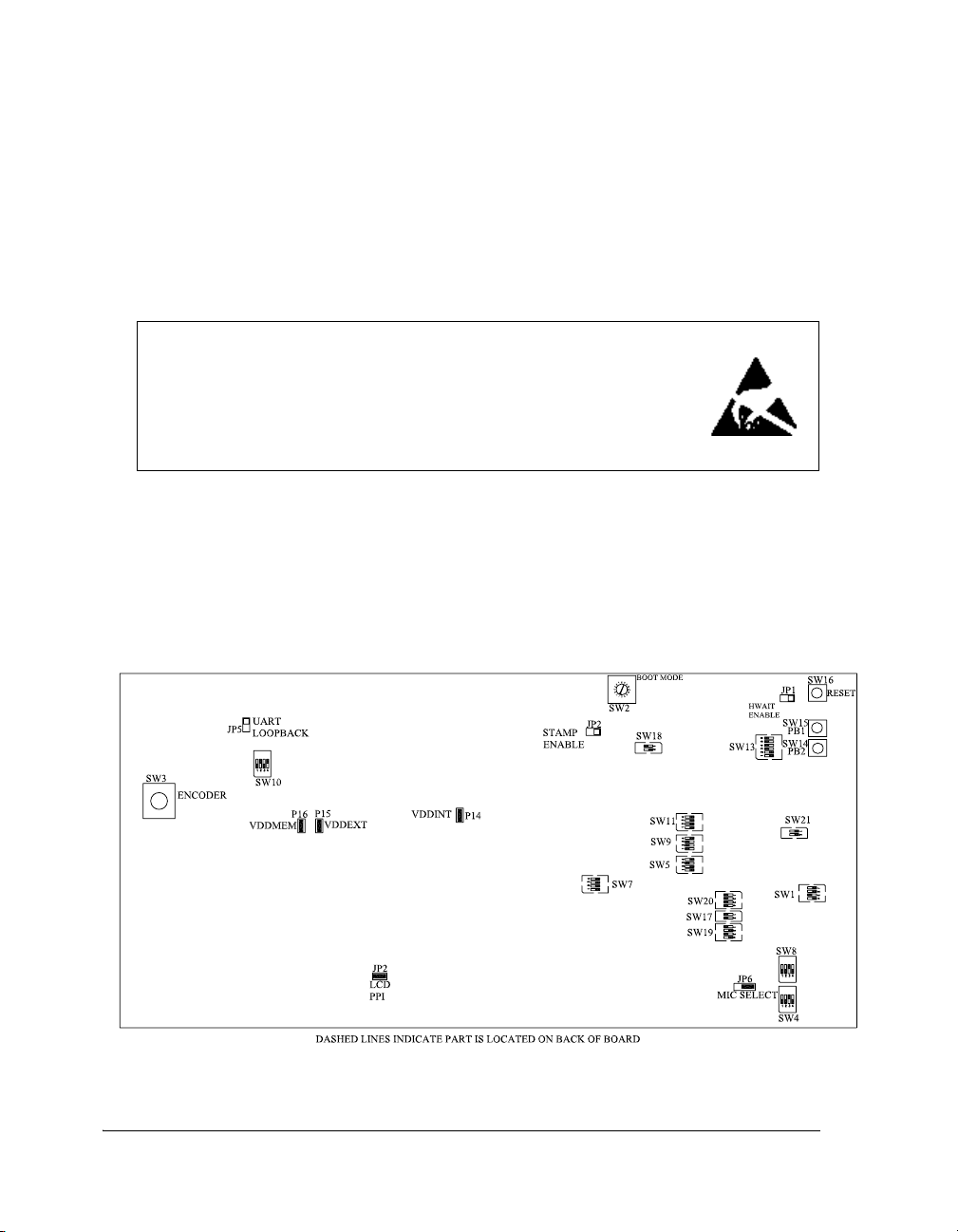
board carefully to avoid the discharge of static electricity, which can damage some components. Figure 1-1 shows the default jumper settings,
switches, connector locations, and LEDs used in installation. Confirm
that your board is in the default configuration before using the board.
Figure 1-1. EZ-KIT Lite Hardware Setup
1-4 ADSP-BF527 EZ-KIT Lite Evaluation System Manual
Page 29

Using ADSP-BF527 EZ-KIT Lite
Installation and Session Startup
For correct operation, install the software and hardware in the order presented in the VisualDSP++ Installation Quick Reference Card.
L
There are two USB interfaces on the ADSP-BF527 EZ-KIT Lite.
Be sure to use the debugger’s interface (ZJ1) when connecting your
computer to the board with provided USB cable. The other USB
interface (labelled USB-OTG, P1) is for applications use.
1. Verify that the yellow USB monitor LED (ZLED3, located near the
USB connector) is lit. This signifies that the board is communicating properly with the host PC and is ready to run VisualDSP++.
2. If you are running VisualDSP++ for the first time, navigate to the
VisualDSP++ environment via the Start–>Programs menu. The
main window appears. Note that VisualDSP++ does not connect to
any session. Skip the rest of this step to step 3.
If you have run VisualDSP++ previously, the last opened session
appears on the screen. You can override the default behavior and
force VisualDSP++ to start a new session by pressing and holding
down the Ctrl key while starting VisualDSP++. Do not release the
Ctrl key until the Session Wizard appears on the screen. Go to
step 4.
3. To connect to a new EZ-KIT Lite session, start Session Wizard by
selecting one of the following.
• From the Session menu, New Session.
• From the Session menu, Session List. Then click New Ses-
sion from the Session List dialog box.
• From the Session menu, Connect to Target.
ADSP-BF527 EZ-KIT Lite Evaluation System Manual 1-5
Page 30

Installation and Session Startup
4. The Select Processor page of the wizard appears on the screen.
Ensure Blackfin is selected in Processor family. In Choose a target
processor, select ADSP-BF527. Click Next.
5. The Select Connection Type page of the wizard appears on the
screen. Select EZ-KIT Lite and click Next.
6. The Select Platform page of the wizard appears on the screen.
Ensure that the selected platform is ADSP-BF527 EZ-KIT Lite via
Debug Agent. Specify your own Session name for the session or
accept the default name.
The session name can be a string of any length; although, the box
displays approximately 32 characters. The session name can
include space characters. If you do not specify a session name,
VisualDSP++ creates a session name by combining the name of the
selected platform with the selected processor. The only way to
change a session name later is to delete the session and to open a
new session.
Click Next.
7. The Finish page of the wizard appears on the screen. The page dis-
plays your selections. Check the selections. If you are not satisfied,
click Back to make changes; otherwise, click Finish. VisualDSP++
creates the new session and connects to the EZ-KIT Lite. Once
connected, the main window’s title is changed to include the session name set in step 6.
L
1-6 ADSP-BF527 EZ-KIT Lite Evaluation System Manual
To disconnect from a session, click the disconnect button
or select Session–>Disconnect from Target.
To delete a session, select Session –> Session List. Select the ses-
sion name from the list and click Delete. Click OK.
Page 31

Using ADSP-BF527 EZ-KIT Lite
Evaluation License Restrictions
The ADSP-BF527 EZ-KIT Lite installation is part of the VisualDSP++
installation. The EZ-KIT Lite is a licensed product that offers an unrestricted evaluation license for the first 90 days. Once the initial
unrestricted 90-day evaluation license expires:
• VisualDSP++ restricts a connection to the ADSP-BF527 EZ-KIT
Lite via the USB debug agent interface only. Connections to simulators and emulation products are no longer allowed.
• The linker restricts a user’s program to 20 KB of memory for code
space with no restrictions for data space.
• The EZ-KIT Lite hardware must be connected and powered up to
use VisualDSP++ with a valid evaluation or permanent license.
Refer to the VisualDSP++ Installation Quick Reference Card for details.
Memory Map
The ADSP-BF527 processor has internal static random access memory
(SRAM) used for instructions or data storage. See Table 1-1. The internal
memory details can be found in the ADSP-BF2x Blackfin Processor Hard-
ware Reference.
The ADSP-BF527 EZ-KIT Lite board includes four types of external
memory: synchronous dynamic random access memory (SDRAM), serial
peripheral interconnect (SPI), parallel flash, and NAND flash. See
Table 1-2. For more information about a specific memory type, go the
respective section in this chapter.
ADSP-BF527 EZ-KIT Lite Evaluation System Manual 1-7
Page 32

Memory Map
Table 1-1. EZ-KIT Lite Internal Memory Map
Start Address Content
0xEF00 0000 BOOT ROM (32K BYTE)
0xEF00 8000
0xFEB0 0000
0xFEB2 0000
0xFF40 0000
0xFF40 4000
0xFF40 8000
0xFF50 0000
0xFF50 4000
0xFF50 8000
0xFF60 0000
0xFF60 4000
0xFF60 8000
0xFF60 C000
0xFF61 0000
0xFF61 4000
0xFF70 0000
0xFF70 1000
Reserved
0xFF80 0000 L1 DATA BANKA SRAM (16K BYTE)
0xFF80 4000 L1 DATA BANKA SRAM/CACHE (16K BYTE)
0xFF80 8000 Reserved
0xFF90 0000 L1 DATA BANKB SRAM (16K BYTE)
0xFF90 4000 L1 DATA BANKB SRAM/CACHE (16K BYTE)
0xFF90 8000 Reserved
0xFFA0 0000 L1 INSTRUCTION BANKA LOWER SRAM (16K BYTE)
0xFFA0 4000 L1 INSTRUCTION BANKA UPPER SRAM (16K BYTE)
0xFFA0 8000 L1 INSTRUCTION BANKB LOWER SRAM (16 BYTE)
0xFFA0 C000 Reserved
0xFFA1 0000 L1 INSTRUCTION SRAM/CACHE (16K BYTE)
1-8 ADSP-BF527 EZ-KIT Lite Evaluation System Manual
Page 33

Using ADSP-BF527 EZ-KIT Lite
Table 1-1. EZ-KIT Lite Internal Memory Map (Cont’d)
Start Address Content
0xFFA1 4000
0xFFA1 8000
0xFFA1 C000
0xFFA2 0000
0xFFA2 4000
0xFFB0 0000 L1 SCRATCHPAD SRAM (4K BYTE)
0xFFB0 1000 Reserved
0xFFC0 0000 SYSTEM MMR REGISTERS
0xFFE0 0000 CORE MMR REGISTERS
Reserved
Table 1-2. EZ-KIT Lite External Memory Map
Start Address End Address Content
0x0000 0000 0x03FF FFFF SDRAM bank 0 (SDRAM)
0x2000 0000 0x200F FFFF ASYNC memory bank 0 (flash)
0x2010 0000 0x201F FFFF ASYNC memory bank 1 (flash)
0x2020 0000 0x202F FFFF ASYNC memory bank 2 (flash)
0x2030 0000 0x203F FFFF ASYNC memory bank 3 (flash)
0x2040 0000 0xEEFF FFFF Reserved
SDRAM Interface
The ADSP-BF527 processor connects to a 64 MB Micron
MT48LC32M16A2TG-75 chip through the external bus interface unit
(EBIU). The SDRAM chip can operate at a maximum clock frequency of
133 MHz.
With a VisualDSP++ session running and connected to the EZ-KIT Lite
board via the USB debug agent, the SDRAM registers are configured
automatically with values listed in Table 1-3 each time the processor is
ADSP-BF527 EZ-KIT Lite Evaluation System Manual 1-9
Page 34

SDRAM Interface
reset. The values are used whenever SDRAM is accessed through the
debugger (for example, when viewing memory windows or loading a
program).
To disable the automatic setting of the SDRAM registers, select Target
Options from the Settings menu in VisualDSP++ and uncheck Use XML
reset values. For more information on changing the reset values, refer to
the online Help.
Table 1-3. SDRAM Default Settings with a 133 MHz SCLK
Register Value Function
pEBIU_SDRRC 0x0407 Calculated with SCLK = 133 MHz
fSCLK = 133 MHz
tREF = 64 ms
NRA = 8192 row addresses
tRAS = 6 clock cycles
tRP = 2 clock cycles
RDIV = 0x407
pEBIU_SDBCTL 0x0025 EBCAW = 10 bits
EBSZ = 64M byte
EBE = enabled
pEBIU_SDGCTL 0x0091998d TSCSR = 45 degrees C
EMREN = disabled
FBBRW = disabled
PSSE = enables SDRAM powerup sequence on next SDRAM
access
PSM = precharge, 8 BCBR refresh cycles, mode register set
PUPSD = no extra delay added before first precharge command
TWR = 2 cycles
TRCD = 3 cycles
TRP = 3 cycles
TRAS = 6 cycles
PASR = all 4 banks refreshed
CL = CAS latency 3 cycles
SCTLE = CLOUT disabled
1-10 ADSP-BF527 EZ-KIT Lite Evaluation System Manual
Page 35

Using ADSP-BF527 EZ-KIT Lite
Table 1-4 shows the configuration for the PLL registers using a 400 MHz
CCLK and 133 MHz SCLK. The PLL_CTL and PLL_DIV registers are initial-
ized in the user code to achieve maximum performance.
Table 1-4. PLL Register Settings
Register SCLK = 133 MHz
CCLK = 400 MHz
PLL_CTL 16
PLL_DIV 3
An example program is included in the EZ-KIT Lite installation directory
to demonstrate how to setup and access the SDRAM interface. For more
information on how to initialize the registers after a reset, search the VisualDSP++ online Help for “reset values”.
Parallel Flash Memory Interface
The parallel flash memory interface of the ADSP-BF527 EZ-KIT Lite
contains a 4 MB (2M x 16 bits) ST Micro M29W320EB chip. Flash
memory connects to the 16-bit data bus and address lines 1 through 19.
Chip enable is decoded by using AMS0–3 select lines through NAND and
AND gates. The address range for flash memory is
0x203F FFFF.
Flash memory is pre-loaded with boot code for the blink, LCD images,
and power-on-self test (POST) programs. For more information, refer to
“Power-On-Self Test” on page 1-25.
By default, the EZ-KIT Lite boots from the 16-bit parallel flash memory.
The processor boots from flash memory if the boot mode select switch
SW2) is set to a position of 1 (see “Boot Mode Select Switch (SW2)” on
(
page 2-11).
ADSP-BF527 EZ-KIT Lite Evaluation System Manual 1-11
0x2000 0000 to
Page 36

NAND Flash Interface
Flash memory code can be modified. For instructions, refer to the online
Help and example program included in the EZ-KIT Lite installation
directory.
NAND Flash Interface
The ADSP-BF527 processor is equipped with an internal NAND flash
controller, which allows the 4 Gbit ST Micro’s NAND04 device to be
attached gluelessly to the processor. NAND flash is attached via the processor’s specific NAND flash control and data lines. NAND flash shares
pins with the Ethernet PHY, host connector, and expansion interface.
The NAND chip enable signal (NDCE#_HOSTD10) can be disconnected from
NAND flash by turning OFF SW11.4 (switch 11 position 4). This ensures
that the NAND will not be driving data when HOSTD10 changes state. See
“Rotary NAND Enable Switch (SW11)” on page 2-16 for more
information.
The Ethernet PHY (U14) must be disabled in order for NAND flash to
function properly. This is accomplished by setting SW1 to OFF, OFF, ON,
OFF.
For more information about the NAND04 device, refer to the ST Microelectronics Web site at:
http://www.st.com/stonline/products/families/memories/memory/index.htm
.
An example program is included in the EZ-KIT Lite installation directory
to demonstrate how to setup and access the NAND flash interface.
1-12 ADSP-BF527 EZ-KIT Lite Evaluation System Manual
Page 37

Using ADSP-BF527 EZ-KIT Lite
SPI Interface
The ADSP-BF527 processor has one serial peripheral interface (SPI) port
with multiple chip select lines. The SPI port connects directly to serial
flash memory, MAX1233 touchscreen and keypad controller, audio codec,
and expansion interface.
Serial flash memory is a 16 Mb ST Micro M25P16 device, which is
selected using the SPISEL1 line of the processor. SPI flash memory is
pre-loaded with boot code for the blink and POST programs. For more
information, refer to “Power-On-Self Test” on page 1-25. By default, the
EZ-KIT Lite boots from the 16-bit flash parallel memory. SPI flash can be
selected as the boot source by setting the boot mode select switch (SW2) to
position 3 (see “Boot Mode Select Switch (SW2)” on page 2-11).
SPI flash code can be modified. For instructions, refer to the VisualDSP++
online Help and example program included in the EZ-KIT Lite installation directory.
By default, the EZ-KIT Lite is set to use the SPISEL2 pin as the chip select
for the MAX1233 touchscreen and keypad controller (see “KEY/PEN CS
Switch (SW18)” on page 2-19). SPISEL2 is shared with the CDG signal,
which is connected to the rotary encoder. It is important not to use the
rotary encoder while trying to access the MAX1233 controller. Shutting
OFF SW11.2 disables the rotary encoder. See “Rotary Encoder Interface” on
page 1-17 for more information. There are also provisions to use the
SPISEL4 signal as the MAX1233 chip select by setting SW18 to OFF, ON.
SPISEL4 signal is shared with the ERXD1_HOSTD8 signal. Using signal
SPISEL4 will interfere with the ability to use Ethernet, but will allow the
use of rotary, keypad, and touchscreen, all at the same time. The appropriate port function needs to be set up to use programmable flag (PF)
the processor as
SPISEL4 (refer to the hardware reference manual for
PH8 of
details). For more information, refer to “Touchscreen and Keypad Inter-
face” on page 1-16.
ADSP-BF527 EZ-KIT Lite Evaluation System Manual 1-13
Page 38

PPI Interface
By default, the audio codec is setup to use the
SPISEL5 signal as the SPI
chip select when configuring the codec. The chip select is shared with the
HOSTD9 signal. For more information, refer to see “Audio Interface” on
page 1-19.
PPI Interface
The ADSP-BF527 processor provides a parallel peripheral interface (PPI),
supporting data widths up to 16 bits. The PPI interface provides three
multiplexed frame syncs, a dedicated clock input, and 16 data lines. The
EZ-KIT Lite uses an eight-bit data connection to the TFT LCD module.
The full PPI port is accessible on the PPI connector P8 and expansion
interface.
The PPI interface can be disconnected from the LCD module by removing jumper on JP2. The JP2 jumper enables the U31 and U32 buffer ICs.
For more information on the LCD module, refer to “LCD Module Inter-
face” on page 1-15. For information on how to enable the PPI connection
to the LCD module, see “LCD PPI Jumper (JP2)” on page 2-21.
The PPI signals connect to multi-function pins; the upper eight data bit
signals are configured for the rotary, SPI, UART1, and LED0 interfaces. See
“Touchscreen and Keypad Interface” on page 1-16 for more information.
The PPI interface has a dedicated clock, generated from an on-board oscillator (default) or the expansion interface. The source of the PPI clock can
be configured by software via the PPI_SEL signal. The signal connects to
the processor’s flag pin PG12 by setting SW13 position 4 ON. Flag pin PG12 is
shared with the
HOSTACK and LED2 are not available. The PPISEL signal does not need to be
driven if the default on-board oscillator is used;
HOSTACK_LED2 signal. When the clock select line is used,
PPISEL is driven when the
expansion interface is used as the clocking source. Refer to “GPIO Enable
Switch (SW13)” on page 2-16 for more information.
1-14 ADSP-BF527 EZ-KIT Lite Evaluation System Manual
Page 39

Using ADSP-BF527 EZ-KIT Lite
LCD Module Interface
The EZ-KIT Lite features a Varitronix VL_PS_COG_T350MCQB TFT
LCD module with touchscreen overlay. This is a 3.5” landscape display
with a resolution of 320 x 240 and a color depth of 24 bits. The interface
is an RGB-888 serial parallel interface, eight bits of red, followed by eight
bits of green, and then eight bits of blue.
To configure the PPI interface, refer to the LCD software example located
in the…\Blackfin\Examples\ADSP-BF527 EZ-KIT Lite\POST subdirectory
of the VisualDSP++ installation directory. The values are obtained from
the timing characteristics section of the VL_PS_COG_T350MCQB
datasheet.
The interface is set to control frame sync 1 and 2 (PPIFS1, PPIFS2)
natively from the ADSP-BF527 processor. The LCD data enable (DEN) is
controlled by a Xilinx CPLD XC9536XL. You do not need to change
CPLD code, which should work for the VL_PS_COG_T350MCQB display. The verilog source code for the CPLD can be found in the reference
resource zip file at:
http://www.analog.com/en/epHSProd/0,,BF527-HARDWARE,00.html.
The LCD module can be disconnected from PPI by removing the jumper
on JP2. Refer to “LCD PPI Jumper (JP2)” on page 2-21 for more
information.
ADSP-BF527 EZ-KIT Lite Evaluation System Manual 1-15
Page 40

Touchscreen and Keypad Interface
Touchscreen and Keypad Interface
The MAX1233 touchscreen and keypad controller connects to the SPI
interface of the ADSP-BF527 processor and uses the SPISEL2 signal. The
controller provides the X and Y positions, as well as a measurement for the
pressure applied to the touchscreen. The touchscreen can be used with
either a stylus or a finger.
Two interrupt signals connect to the device:
• The key interrupt (KEYIRQ#) signal is mapped to PF9 and used to
notify the processor that a key on the keypad has been pressed.
• The pen interrupt (PENIRQ#) signal is mapped to PF10 and used to
notify the processor that the screen has been touched. The PENIRQ#
signal is shared with UART1RTS.
SW5 positions 1 and 2 are ON by default and allow the MAX1233 controller
to be disconnected from PF pins PF9 and PF10 of the processor.
SW5 positions 3 and 4 are (OFF, ON) by default and select the board reset as
the reset input to the LCD module. The GPIO function of PF PG11 also
can be used to control the LCD reset (SW5 positions 3 and 4 ON and OFF);
however, PG11 is used to control LED1 by default.
The EZ-KIT Lite features a 4 x 4 keypad assembly connected to the
MAX1233 touchscreen controller (U16). The keypad interface connects to
the EZ-KIT Lite via a nine-pin connector (
P2). The ADSP-BF527 proces-
sor receives input from the keypad through the SPI interface after a
KEYIRQ# interrupt. The row/column pull-ups and pull-downs are handled
internally by the MAX1233 controller.
For more options on the MAX1233 controller, refer to “Keypad LCD
Enable Switch (SW5)” on page 2-13.
An example program is included in the EZ-KIT Lite installation directory
to demonstrate how to setup and access the touchscreen and keypad
interface.
1-16 ADSP-BF527 EZ-KIT Lite Evaluation System Manual
Page 41

Using ADSP-BF527 EZ-KIT Lite
Rotary Encoder Interface
The ADSP-BF527 processor has a built-in, up-down counter with support
for a rotary encoder. The three-wire rotary encoder interface connects to
the rotary switch (SW3) and expansion interface connector. The rotary
encoder can be turned clockwise for the up function, counter clockwise
for the down function, or can be used as a push button for clearing the
counter.
The rotary switch is a two-bit quadrature (Gray code) counter with
detent, meaning that both the down signal (CDG) and up signal (CUD) will
toggle when the count register increases on a rotation to the right. Upon
rotating to the left, both CDG and CUD will toggle, and the over all count
decreases.
If the processor pins are needed for the expansion interface, disconnect the
rotary encoder switch via the four-position rotary NAND enable switch
(SW11). For more information, see “Rotary NAND Enable Switch
(SW11)” on page 2-16.
The CDG signal is shared with the SPISEL2 signal; care must be taken not to
rotate the switch while issuing SPI commands to the keypad and touchscreen controller. To ensure that there is no interference from the rotary
encoder on SPISEL2, turn SW1 position 2 OFF. Shutting off connection to
CDG causes the rotary switch not to operate correctly. Both CDG and CUD are
necessary for the switch to output accurate counts.
An example program is included in the EZ-KIT Lite installation directory
to demonstrate how to setup and access the rotary encoder interface.
ADSP-BF527 EZ-KIT Lite Evaluation System Manual 1-17
Page 42

Ethernet Interface
Ethernet Interface
The ADSP-BF527 processor has an integrated Ethernet MAC with media
independent interface (MII) and reduced media independent interface
(RMII), which connects to an external PHY. The EZ-KIT Lite provides a
SMSC LAN8700 RMII Ethernet PHY with Auto-MDIX, fully compliant
with IEEE 802.2/802.2u standards. The SMSC LAN8700 chip supports
10BASE-T and 100BASE-TX operations. The part is attached gluelessly
to the processor.
The Ethernet signals are shared with NAND flash, and the Ethernet is by
default turned off (SW1 OFF, OFF, ON, OFF). See “ETH Enable Switch
(SW1)” on page 2-9 for more information. It is important not to run code
that accesses the NAND while using the Ethernet interface.
The Ethernet mode is set by the SW9 switch and defaults to all capable,
auto negotiation with settings OFF, OFF, OFF, ON. See “ETH Mode Flash CS
Switch (SW9)” on page 2-15 for more information.
The Ethernet chip is pre-loaded with a MAC address for the EZ-KIT Lite.
The MAC address is stored in the public one-time programmable (OTP)
memory of the processor and can be found on a sticker on the bottom side
of the EZ-KIT Lite.
The PHY portion of the Ethernet chip connects to a Pulse HX1188 (U26)
magnetics, then to a standard RJ-45 Ethernet connector (
information, see “Ethernet Connector (J9)” on page 2-28.
Example programs are included in the EZ-KIT Lite installation directory
to demonstrate how to use the Ethernet interface.
1-18 ADSP-BF527 EZ-KIT Lite Evaluation System Manual
J9). For more
Page 43

Using ADSP-BF527 EZ-KIT Lite
Audio Interface
The audio interface of the EZ-KIT Lite consists of a low-power stereo
codec with integrated headphone driver and its associated passive components. There are two inputs, stereo line in, and mono microphone as well
as two outputs, headphone, and stereo line out. The codec has integrated
stereo analog-to-digital converters (ADCs) and digital-to-analog converters (DACs) and requires minimal external circuitry.
The codec connects to the ADSP-BF527 processor via the processor’s
serial port 0A (alternate). The SPORT0A port is disconnected from the
codec by turning SW17 and SW20. This allows SPORT0A to be used on the
expansion interface.
The TFS0A signal is shared with the Ethernet and host connectors, as well
as the RMIIMDINT# and HOSTCE# signals. SW21 allows this signal to be disconnected from the host connector by setting position 1 OFF, and STAMP
connectors position 2 OFF. To connect signal TFSOA_RMIIMDINT#_HOSTCE#
to either interface, turn the corresponding switch position ON. Refer to
“TFS0A/HOSTCE Enable Switch (SW21)” on page 2-19 for more
information.
The control interface for the codec is selectable by the SW8 and SW19
switches between the two-wire interface (TWI) and SPI. The board
default is SPI mode, set by the
SW8 switch positions 3 ON and 4 OFF. To select TWI mode, turn SW8
positions 3
OFF and 4 ON, as well as SW19 (OFF, ON, OFF, ON). Refer to
SW19 switch (ON, OFF, ON, OFF) and by the
“Mic/HP LPBK Audio Mode Switch (SW8)” on page 2-14 and “SPI/TWI
Switch (SW19)” on page 2-19 for more information.
Mic gain is selectable through the
or –6 dB, by turning
must be
OFF to achieve the desired gain. Refer to “MIC Gain Switch
ON position 1, 2, or 3 respectively. All other positions
SW4 switch, with values of 14 dB, 0 dB,
(SW4)” on page 2-12 for more information.
ADSP-BF527 EZ-KIT Lite Evaluation System Manual 1-19
Page 44

USB OTG Interface
Microphone bias is provided through a low-noise reference voltage. A
jumper on position 2 and 3 of
JP6 connects the MICBIAS to the audio jack.
Placing the jumper on positions 1 and 2 of JP6 connects the bias directly
to the mic signal. Refer to “MIC Select Jumper (JP6)” on page 2-22 for
more information.
J7 and J8 are 3.5 mm connectors for the audio portion of the board. J7
connects the mic on the top portion and line-in on the bottom. J8 connects the headphone on the top portion and line-out on the bottom. If
there is no 3.5 mm cable plugged into the bottom of J7 or J8, the signals
are looped back inside the connector.
For testing purposes, SW8 positions 1 and 2 allow the MICIN signal to be
connected to either the left or right headphone. Do not connect both left
and right to the MICIN signal at the same time—only position 1 or 2 of SW8
should be ON at the same time. Refer to “Mic/HP LPBK Audio Mode
Switch (SW8)” on page 2-14 for more information.
For more information, see “Dual Audio Connectors (J7–8)” on page 2-28.
The EZ-KIT Lite is shipped with a headphone and multiple 3.5 mm
cables, which allow you to run the example programs provided in the
EZ-KIT Lite installation directory and learn about the audio interface.
USB OTG Interface
The ADSP-BF527 processor has a built-in, high-speed USB on-the-go
(OTG) interface and integrated PHY. The interface connects to a
24 MHz clock (
or device. When in device mode, the USB 5V regulator (
switch (U28) are turned OFF. When in host mode, the USB 5V regulator
and FET are turned
1-20 ADSP-BF527 EZ-KIT Lite Evaluation System Manual
U12), has surge protection, and can be configured as a host
VR3) and FET
ON and can supply 5V at 500 mA.
Page 45

Using ADSP-BF527 EZ-KIT Lite
The control mechanism to turn the two devices on and off are via the
flag pin of the processor and must be connected on the board to signal
USB_VRSEL through switch SW13. By default, USB_VRSEL is held low or a
logic 0 via a pull-down resistor, and both devices are turned off. To use
host mode and provide 5V to a device, SW13 position 2 needs to be turned
OFF and position 6 ON. This disables push button 2. Note that signal
USB_VRSEL is shared with HOSTADDR. The default for positions 2 and 6 of
SW13 are ON and OFF, which shuts off the VR3 regulator and U28 FET. For
more information, see “GPIO Enable Switch (SW13)” on page 2-16.
The USB OTG interface has a mini-AB connector (P1); cables that plug
into P1 are shipped with the EZ-KIT Lite.
Use the example programs in the EZ-KIT Lite installation directory to
learn about the ADSP-BF527 processor’s device and host modes. For
more information about the USB interface, refer to the ADSP-BF52x
Blackfin Processor Hardware Reference.
UART Interface
The ADSP-BF527 processor has two built-in universal asynchronous
receiver transmitters (UARTs). UART1—0 share the processor pins with
other peripherals on the EZ-KIT Lite.
PG13
UART1 has full RS-232 functionality via the Analog Devices 3.3V
ADM3202 (U25) line driver and receiver. The UART can be disconnected
from the ADM3202 by turning
OFF all positions of SW10. See “UART
Enable Switch (SW10)” on page 2-15. When using UART1, jumpers JP5
should not be installed.
JP5 is a UART loopback jumper and should be
installed only when running the POST program. If signals RTS and CTS are
needed for flow control, the
figured as a GPIO for
RTS. The HWAIT port pin PG0 can be used for CTS by
UART1RTS_PENIRQ# port pin PF10 can be con-
setting up the pin accordingly. See “UART1 Loopback Jumper (JP5)” on
page 2-22 and “UART Enable Switch (SW10)” on page 2-15 for more
information.
ADSP-BF527 EZ-KIT Lite Evaluation System Manual 1-21
Page 46

RTC Interface
UART0 and UART1 are connected to the expansion interface. UART0 of the
processor also is available via a STAMP connector (P5). See “UART0
Connector (P5)” on page 2-29.
Example programs are included in the EZ-KIT Lite installation directory
to demonstrate UART and RS-232 operations.
For more information on the UART interface, refer to the ADSP-BF52x
Blackfin Processor Hardware Reference.
RTC Interface
The ADSP-BF527 processor has a real-time clock (RTC) and a watchlog
timer. Typically the RTC interface is used to implement a real-time
watchlog or life counter of the time elapsed since the last system reset. The
EZ-KIT Lite is equipped with a Sanyo (CR2430) lithium coin 3V battery
supplying 280 mAh. The 3V battery and the 3.3V supply of the board
connect to the RTC power pin of the processor. When the EZ-KIT Lite is
powered, the RTC circuit uses the board power to supply voltage to the
RTC pin. When the EZ-KIT Lite is not powered, the RTC circuit uses the
lithium battery to maintain the power to the RTC pin. After removing the
mylar, the battery will last for about 1 year with the EZ-KIT Lite
unpowered.
Example programs are included in the EZ-KIT Lite installation directory
to demonstrate the RTC features.
L
For more information on the RTC and watchdog timer, refer to the
ADSP-BF52x Blackfin Processor Hardware Reference.
1-22 ADSP-BF527 EZ-KIT Lite Evaluation System Manual
The EZ-KIT Lite is shipped with a protective Mylar sheet placed
between the coin battery and the positive pin of the battery holder.
Please remember to remove the Mylar sheet before trying to use
RTC functionality of the processor.
Page 47

Using ADSP-BF527 EZ-KIT Lite
LEDs and Push Buttons
The EZ-KIT Lite provides two push buttons and three LEDs for general-purpose I/O.
The three LEDs, labeled LED1 through LED3, are accessed via the PF8, PG11,
and PG12 pins of the processor respectively. For information on how to
program the pins, refer to the ADSP-BF52x Blackfin Processor Hardware
Reference.
LED1 is shared with signal HOSTWR#, while LED2 is shared with signal HOSTACK
. The LED1 signal can be used for the LCD reset by turning SW5
positions 3 ON and 4 OFF. LED2 is shared with PPI_SEL; turn SW13
position 4 OFF to use the LED.
The two general-purpose push buttons are labeled PB1 and PB2. The status
of each individual button can be read through programmable flag inputs,
PG0 and PG13. The flag reads 1 when a corresponding switch is being
pressed. When the switch is released, the flag reads 0. A connection
between the push button and processor input is established through the
SW13 DIP switch. Push button 1 is shared with HWAIT and alternatively can
be connected to signal keypad_busy by setting SW13 position 1 OFF and
position 5 ON. Push button 2 is shared with HOSTADDR and also can be connected to USB_VRSEL by setting SW13 position 2 OFF and position 6 ON.
USB_VRSEL allows the USB OTG to power an external USB device with
5V. See “USB OTG Interface” on page 1-20 and “GPIO Enable Switch
(SW13)” on page 2-16 for more information.
An example program is included in the EZ-KIT Lite installation directory
to demonstrate functionality of the LEDs and push buttons.
ADSP-BF527 EZ-KIT Lite Evaluation System Manual 1-23
Page 48

JTAG Interface
JTAG Interface
The JTAG emulation port allows an emulator to access the processor’s
internal and external memory through a six-pin interface. The JTAG emulator port of the processor can be accessed via the on-board USB debug
agent or with an external emulator via the JTAG connector (ZP4). When
an external emulator connects to the board, the on-board USB debug
agent is disabled. See “JTAG Connector (ZP4)” on page 2-33 for more
information.
For more information about emulators, contact Analog Devices or go to:
http://www.analog.com/processors/blackfin/evaluationDevelop
ment/crosscore/.
Expansion Interface
The expansion interface consists of three 90-pin connectors (J1—3). These
connectors contain a majority of the ADSP-BF527 processor’s signals. For
the pinout of the connectors, go to “ADSP-BF527 EZ-KIT Lite Sche-
matic” on page B-1. The expansion interface allows an EZ-Extender or a
custom-design daughter board to be tested across various hardware platforms. The mechanical dimensions of the expansion connectors can be
obtained by contacting Technical or Customer Support.
Analog Devices offers many EZ-Extender products. For more information
about EZ-Extenders, visit the Analog Devices Web site at:
http://www.analog.com/processors/blackfin/evaluationDevelopment/crosscore/
Limits to current and interface speed must be taken into consideration
when using the expansion interface. Because current for the expansion
interface is sourced from the EZ-KIT Lite, the current should be limited
to 1A for both the 5V and 3.3V planes. If more current is required, then a
1-24 ADSP-BF527 EZ-KIT Lite Evaluation System Manual
.
Page 49

Using ADSP-BF527 EZ-KIT Lite
separate power connector and a regulator must be designed on a daughter
card. Additional circuitry can add extra loading to signals, decreasing their
maximum effective speed.
L
Analog Devices does not support and is not responsible for the
effects of additional circuitry.
Power Measurements
Several locations are provided for measuring the current draw from various power planes. Precision 0.05 ohm shunt resistors are available on the
VDDINT, VDDEXT, and VDDMEM pins. For the current draw measuments, the
associated jumper (P14, P15, or P16) should be removed. Once the jumper
is removed, the voltage across the resistor can be measured using an oscilloscope. Once the voltage is measured, the current can be calculated by
dividing the voltage by 0.05. For the highest accuracy, a differential probe
should be used for measuring the voltage across the resistor.
For more information, see “VDDINT Power Jumper (P14)”, “VDDEXT
Power Jumper (P15)”, and “VDDMEM Power Jumper (P16)” on
page 2-23.
Power-On-Self Test
Once assembled, each EZ-KIT Lite is fully tested for an extended period
of time with a power-on-self test (POST). The POST tests all EZ-KIT
Lite peripherals and validates functionality as well as connectivity to the
processor. The POST is loaded into the parallel flash memory (
SPI flash memory (
pressing the associated push button(s). The POST also can be used as a
reference for a custom software design or hardware troubleshooting.
ADSP-BF527 EZ-KIT Lite Evaluation System Manual 1-25
U8), which can be activated by resetting the board and
U5) and
Page 50

Example Programs
When running the POST, you may need to place switches and jumpers in
specific test modes. In some instances, such as Ethernet, you may need to
plug in an Ethernet loopback connector (provided with the EZ-KIT Lite)
to run the POST. The user LEDs (
cific tests have passed or failed.
The POST program is included in the EZ-KIT Lite installation directory.
For more information, refer to the readme file in the POST directory.
LED1–3) will convey whether the spe-
Example Programs
Example programs are provided with the ADSP-BF527 EZ-KIT Lite to
demonstrate various capabilities of the evaluation board. These programs
are installed with the EZ-KIT Lite software and can be found in the
…\Blackfin\Examples\ADSP-BF527 EZ-KIT Lite subdirectory of the Visu-
alDSP++ installation directory. Refer to the readme file provided with
each example for more information.
Background Telemetry Channel
The ADSP-BF527 USB debug agent supports the background telemetry
channel (BTC), which facilitates data exchange between VisualDSP++ and
the processor without interrupting processor execution.
The BTC allows you to view a variable as it is updated or changed, all
while the processor continues to execute. For increased performance of the
BTC, including faster reading and writing, please check our latest line of
processor emulators at:
http://www.analog.com/processors/blackfin/evaluationDevelopment/crosscore/. For more information about the background telemetry
channel, see the online Help.
1-26 ADSP-BF527 EZ-KIT Lite Evaluation System Manual
Page 51

Using ADSP-BF527 EZ-KIT Lite
Design Reference Information
A design reference info package is available for download on the Analog
Devices Web site. The package provides information on the design, layout, fabrication, and assembly of the EZ-KIT Lite.
The information can be found at:
http://www.analog.com/en/epHSProd/0,,BF527-HARDWARE,00.html.
ADSP-BF527 EZ-KIT Lite Evaluation System Manual 1-27
Page 52

Design Reference Information
1-28 ADSP-BF527 EZ-KIT Lite Evaluation System Manual
Page 53

2 ADSP-BF527 EZ-KIT LITE
HARDWARE REFERENCE
This chapter describes the hardware design of the ADSP-BF527 EZ-KIT
Lite board.
The following topics are covered.
• “System Architecture” on page 2-2
Describes the configuration of the ADSP-BF527 EZ-KIT Lite
board and explains how the board components interface with the
processor.
• “Programmable Flags” on page 2-3
Shows the location and describes the function of the programming
flags (PFs).
• “Push Button and Switch Settings” on page 2-9
Shows the location and describes the function of the push buttons
and switches.
• “Jumpers” on page 2-20
Shows the location and describes the function of the configuration
jumpers.
• “LEDs” on page 2-23
Shows the location and describes the function of the LEDs.
• “Connectors” on page 2-25
Shows the location and provides the part number for all of the connectors on the board. Also, the manufacturer and part number
information is provided for the mating parts.
ADSP-BF527 EZ-KIT Lite Evaluation System Manual 2-1
Page 54

System Architecture
System Architecture
This section describes the processor’s configuration on the EZ-KIT Lite
board (Figure 2-1).
JTAG
Header
USB
Conn
USB
OTG
Conn
RJ11
16 Mb
SPI Flash
+7V
Connector
Debug
24 MHz
Oscillator
Ethernet Phy
Agent
RMII
32.768 KHz
Oscillator
IDC
Conn
Power
Regulation
25 MHz
Oscillator
+3.0 LI-ION
RTC Battery
RTC
Port
JTAG
CLKIN
64 MB
SDRAM
(32M x 16)
EBIU
ADSP-BF527
DSP
600 MHz
LFBGA-SS2, 12mmX12mm/0.5 pitch
MAC USB
UARTs
ADM3202
RS-232
TX/RX
RS-232
Female
289, 4L, (A02)
SPI
SPI
IDC
Conn
MAX1233 keypad/
touch screen Controller
4X4 Keypad
And
SPORTs PPI
Conn
IDC
PPI
Audio
Codec
Internal
Stacked
Die
IDC
Conn
(2)
4 MB
Flash
(2M x 16 )
NAND
TWI
IDC
Conn
12 MHz
Oscillator
4 Gb
NAND Flash
(512M x 8 )
CNTR
UP/DOWN
HOST
PORT
Expansion
Connectors
(3)
Rotary
LEDs (3)
PBs (2)
IDC
Conn
LCD (8Bit max)
QVGA Landscape
Figure 2-1. System Architecture
This EZ-KIT Lite is designed to demonstrate the capabilities of the
ADSP-BF527 Blackfin processors. The processor has an I/O voltage of
3.3V. The core voltage of the processor is controlled by the internal voltage regulator.
2-2 ADSP-BF527 EZ-KIT Lite Evaluation System Manual
Page 55

ADSP-BF527 EZ-KIT Lite Hardware Reference
The core voltage and clock rate can be set on the fly by the processor. The
input clock is 25 MHz. A 32.768 kHz crystal supplies the real-time clock
(RTC) inputs of the processor. The default boot mode for the processor is
external parallel flash boot. See “Boot Mode Select Switch (SW2)” on
page 2-11 for information on how to change the default boot mode.
Programmable Flags
The processor has 50 general-purpose input/output (GPIO) signals spread
across four ports (PF, PG, PH, and PJ). The pins are multi-functional and
depend on the ADSP-BF527 processor setup. The following tables show
how the programmable flag pins are used on the EZ-KIT Lite.
• PF programmable flag pins – Table 2-1
• PG programmable flag pins – Table 2-2
• PH programmable flag pins – Table 2-3
• PJ programmable flag pins – Table 2-4
Table 2-1. PF Port Programmable Flag Connections
Processor Pin Other Processor Function EZ-KIT Lite Function
PF0 PPID0/DR0PRI/ND_D0A Default: LCD via U31 buffer.
Expansion interface
PF1 PPID1/RFS0/ND_D1A Default: LCD via U31 buffer.
Expansion interface J1.73, PPI connector P8.9.
PF2 PPID2/RSCLK0/ND_D2 Default: LCD via U31 buffer.
Expansion interface
PF3 PPID3/DT0PRI/ND_D3A Default: LCD via U31 buffer.
Expansion interface
PF4 PPID4/TFS0/ND_D4A/TAC
LK0
Default: LCD via U31 buffer.
Expansion interface
J1.72, PPI connector P8.8.
J1.74, PPI connector P8.10.
J1.75, PPI connector P8.11.
J2.43, PPI connector P8.12.
ADSP-BF527 EZ-KIT Lite Evaluation System Manual 2-3
Page 56

Programmable Flags
Table 2-1. PF Port Programmable Flag Connections (Cont’d)
Processor Pin Other Processor Function EZ-KIT Lite Function
PF5 PPID5/TSCLK0/ND_D5A/T
ACLK1
PF6 PPID6/DT0SEC/ND_D6A/T
ACI0
PF7 PPID7/DR0SEC/ND_D7A/T
ACI1
PF8 PPID8/DR1PRI Default: LED0.
Default: LCD via U31 buffer.
Expansion interface J2.44, PPI connector P8.13.
Default: LCD via U31 buffer.
Expansion interface J2.45, PPI connector P8.14.
Default: LCD via U31 buffer.
Expansion interface
J2.46, PPI connector P8.15.
Expansion interface J1.79, J2.29, J2.47, via quick
switch U34 to the following connectors: VPP board
P4.2, SPORT0 P6.25, SPORT1 P7.8, SPI P9.14,
TWI P10.10, and PPI P8.24.
PF9 PPID9/RSCLK1/SPISEL6# Default: KEYIRQ (U16) via SW5.2.
Expansion interface J2.48, J2.33, SPORT1 connec-
P7.16, and PPI connector P8.17.
tor
PF10 PPID10/PRFS1/SPISEL7# Default: PENIRQ (U16) via SW5.1.
RTS UART1 U25 via SW10.3, expansion interface
J2.31, J2.49, SPORT1 connector P7.7, and PPI
connector
PF11 PPID11/TFS1/CZM Default: CZM rotary (SW3) via SW11.3.
P8.18.
Expansion interface J2.32, J2.50, via quick switch
U34 to the following connectors: PPI P8.19, SPORT1
P7.11.
PF12 PPID12/DT1PRI/SPISEL2
#/CDG
Default: CDG rotary (SW3) via SW11.2.
SPISEL2# keypad/touchscreen controller via SW18.1,
expansion interface J2.30, J2.51, via quick switch
U30 to the following connectors: SPI P9.9, SPORT1
P7.14 and P7.19, PPI P8.20 and P8.26, SPORT0
P6.19.
PF13 PPID13/TSCLK1/SPISEL3
#/CUD
Default: CUD rotary (SW3) via SW11.1.
Expansion interface
U34 to the following connectors: SPORT1 P7.6 and
P7.21, SPORT0 P6.21, PPI P8.21 and P8.25, SPI
P9.12.
J2.34, J2.52, via quick switch
2-4 ADSP-BF527 EZ-KIT Lite Evaluation System Manual
Page 57

ADSP-BF527 EZ-KIT Lite Hardware Reference
Table 2-1. PF Port Programmable Flag Connections (Cont’d)
Processor Pin Other Processor Function EZ-KIT Lite Function
PF14 PPID14/DT1SEC/UART1TX Default: UART1 (U25) TX.
Expansion interface J2.28, J2.53, J2.55, J3.8,
SPORT1 connector P7.12, and PPI connector P8.22.
PF15 PPID15/DR1SEC/UART1RX
/TACI3
Default: UART1 (U25) RX via SW10.2.
Expansion interface
J2.27, J2.54, J2.56, J3.7,
SPORT1 connector P7.10, and PPI connector P8.23
Table 2-2. PG Port Programmable Flag Connections
Processor Pin Other Processor Function EZ-KIT Lite Function
PG0 HWAIT Default: PB1 via SW13.1.
UART1
KEYPAD_BUSY via SW13.1 OFF and SW13.5 ON. Host
connector P13.12, and expansion interface J1.84.
PG1 SPISS#/SPISEL1# Default: SPI flash (U8) CS via SW9.4.
Expansion interface
following connectors: SPI P9.10, PPI P8.27, SPORT0
P6.17, and SPORT1 P7.17.
PG2 SPISCK Default: SPI flash (U8), codec (U2) via SW19.3, key-
pad/touch-screen controller (
Expansion interface J2.9, via quick switch U30 to the
following connectors: SPI P9.8, SPORT0 P6.22,
SPORT1
PG3 SPIMISO/DR0SECA Default: SPI flash (U8), keypad/touchscreen controller
(
Via quick switch (U30) to the following connectors: SPI
P9.6, SPORT0 P6.10 and P6.20, SPORT1 P7.20,
and PPI
CTS (HWAIT) via JP1 and SW10.1,
J2.11, via quick switch U30 to the
U16).
P7.22, and PPI P8.34.
U16).
P8.32, and expansion interface J2.12, J2.35.
PG4 SPIMOSI/DT0SECA Default: SPI flash (U8), codec (U2) via SW19.1, key-
pad/touchscreen controller (
Via quick switch (
SPORT0
P9.5, PPI P8.30, and expansion interface J2.10,
J2.36.
U30) to the following connectors:
P6.12 and P6.18, SPORT1 P7.18, SPI
U16).
ADSP-BF527 EZ-KIT Lite Evaluation System Manual 2-5
Page 58

Programmable Flags
Table 2-2. PG Port Programmable Flag Connections (Cont’d)
Processor Pin Other Processor Function EZ-KIT Lite Function
PG5 TMR1/PPIFS2/TFS0A Default: LCD via buffer (U32).
PPI connector P8.33, expansion interface J2.24.
PG6 DT0PRIA/TMR2/PPIFS3 Default: SPORT0 audio codec (U2) via SW20.2.
PPI connector P8.29, SPORT0 connector P6.14,
Expansion interface
PG7 TMR3/DR0PRIA/UART0TX Default: SPORT0 audio codec (U2) via SW20.3.
Via quick switch (U34) to the following connectors:
UART0 P5.6, SPORT0 P6.8 and P6.28, SPORT1
P7.28, Timers P11.6, and expansion interface J2.37,
J3.6.
J2.38, J2.23.
PG8 TMR4/RFS0A/UART0RX/T
ACI4
PG9 TMR5/RSCLK0A/TACI5 Default: SPORT0 audio codec (U2) via SW17.2.
Default: SPORT0 audio codec (U2) via SW20.4.
Via quick switch (U34) to the following connectors:
SPORT0
P11.8, UART0 P5.10, and expansion interface J2.39,
J3.5.
Via quick switch (
P6.7 and P6.30, SPORT1 P7.30, Timers
U34) to the following connectors:
SPORT0 P6.32 and P6.16, SPORT1 P7.32, Timers
P11.10, and expansion interface J2.41.
PG10 TMR6/TSCLK0A/TACI6 Default: SPORT0 audio codec (U2) via SW17.1.
SPORT0 connector
PG11 TMR7/HOST_WR# Default: LED1.
LCD GPIO reset via
P6.6, expansion interface J2.42.
SW5.3, host connector P13.4, via
quick switch to the following connectors: SPORT0
P6.27, UART0 P5.3, SPORT1 P7.29, TWI P10.9,
P11.3, SPI P9.15, and expansion interface
Timers
J1.80.
PG12 DMAR1/UART1TXA/HOST_
ACK
Default: LED2.
PPI_SEL via SW13.4, host connector P13.10, via quick
switch (
U34) to the following connectors: UART0
P5.5, Timers P11.5, TWI P10.12, SPORT0 P6.29,
SPORT1
J1.81.
P7.31, SPI P9.16, and expansion interface
2-6 ADSP-BF527 EZ-KIT Lite Evaluation System Manual
Page 59

ADSP-BF527 EZ-KIT Lite Hardware Reference
Table 2-2. PG Port Programmable Flag Connections (Cont’d)
Processor Pin Other Processor Function EZ-KIT Lite Function
PG13 DMAR0/UART1RXA/HOST_
ADDR/TACI2
Default: PB2 via SW13.2.
OTG USB_VRSEL via SW13.6 ON and SW13.2 OFF, host
connector P13.8, and expansion interface J1.85.
PG14 TSCLK0A/MDC/HOST_RD# Default: host connector P13.2.13.6
MDIO PHY (U14) via SW1.2, expansion interface J3.41
PG15 TFS0A/MIIPHY-
INT#/RMIIMDINT#/HOST_CE#
Default: SPORT0 audio codec (U2) via SW20.1
RMIIMDINT# PHY (U14), host connector P13.6,
SPORT0 connector P6.11, and expansion interface
J2.40, J3.31.
Table 2-3. PH Port Programmable Flag Connections
Processor Pin Other Processor Function EZ-KIT Lite Function
PH0 ND_D0/MIICRS/RMII-
CRSDV/HOST_D0
PH1 ND_D1/ERXER/HOST_D1 Default: NAND Data 1 (U4).
PH2 ND_D2/MDIO/HOST_D2 Default: NAND Data 2 (U4).
Default: NAND Data 0 (U4).
RMII carrier sense/receive data valid (U14.36), host
connector data 0 (
P13.31), and expansion interface
(J3.40).
PHY receive error (U14.21), host connector data 1
P13.29), expansion interface (J3.39).
(
PHY management bus MDIO via SW1.1, host connector
P13.27), and expansion interface (J3.42).
data 2 (
PH3 ND_D3/ETXEN/HOST_D3 Default: NAND Data 3 (U4).
PHY transmit enable (
U14.6), host connector data 3
(P13.25), and expansion interface (J3.15).
PH4 ND_D4/MIITX-
CLK/RMIIREF_CLK/HOST_
D4
PH5 ND_D5/ETXD0/HOST_D5 Default: NAND Data 5 (U4).
Default: NAND Data 4 (U4).
PHY RMII ref clock (
U24, host connector data 4 (P13.23), and
output
expansion interface (
PHY RMII transmit data 0 (
P13.21), and expansion interface (J3.11).
data 5 (
U14.14) via SW1.3 OFF, oscillator
J3.16).
U14.23), host connector
ADSP-BF527 EZ-KIT Lite Evaluation System Manual 2-7
Page 60

Programmable Flags
Table 2-3. PH Port Programmable Flag Connections (Cont’d)
Processor Pin Other Processor Function EZ-KIT Lite Function
PH6 ND_D6/ERXD0/HOST_D6 Default: NAND Data 6 (U4).
PHY RMII receive data 0 (U14.18), PHY mode via
SW9.3, host connector data 6 (P13.19), and expansion
interface (
PH7 ND_D7/ETXD1/HOST_D7 Default: NAND Data 7 (U4).
PHY RMII transmit data 1 (U14.24), host connector
data 7 (P13.17), and expansion interface (J3.12).
J3.33).
PH8 SPISEL4#/ERXD1/HOST_D
8/TACLK2
Default: NAND Data 7 (U4).
PHY RMII transmit data 1 (
U14.24), keypad/touch-
screen chip select via SW18.2, host connector data 8
(P13.17), and expansion interface (J3.12).
PH9 SPISEL5#/ETXD2/HOST_D
9/TACLK3
Default: SPI SEL5 audio codec U2.
Chip select keypad/touchscreen controller via resistors
U16), host connector data 9 (P13.13), and expansion
(
interface (J3.13).
PH10 ND_CE#_ERXD2/HOST_D10 Default: NAND chip enable via SW11.4 ON.
Host connector data 10 (
P13.17) and expansion inter-
face (J3.35).
PH11 ND_WE/ETXD3/HOST_D11 Default: NAND write enable (U4).
Host connector data 11 (P13.9) and expansion inter-
J3.14).
face (
PH12 ND_RE/ERXD3/HOST_D12 Default: NAND output enable (U4).
Host connector data 12 (
P13.7), expansion interface
(J3.36).
PH13 ND_BUSY/ERXCLK/
HOST_D13
Default: NAND busy (U4).
Host connector data 13 (
P13.5), expansion interface
(J3.38).
PH14 ND_CLE/ERXDV/HOST_D14 Default: NAND command latch enable (U4).
Host connector data 14 (
J3.37).
(
P13.3), expansion interface
PH15 ND_ALE/COL/HOST_D15 Default: NAND address latch enable (U4).
Host connector data 15 (
J3.32).
(
P13.1), expansion interface
2-8 ADSP-BF527 EZ-KIT Lite Evaluation System Manual
Page 61

ADSP-BF527 EZ-KIT Lite Hardware Reference
Table 2-4. PJ Port Programmable Flag Connections
Processor Pin Other Processor
Function
PJ0 PPIFS1/TMR0 Default: PPI frame sync 1 via buffer U32 to LCD conn
PJ1 PPICLK/TMRCLK Default: PPI clock via buffer U32 to LCD conn (P12)
PJ2 SCL Default: not used.
PJ3 SDA Default: not used.
EZ-KIT Lite Function
(P12) and CPLD U33.
PPI connector (
(J2.25).
and CPLD U33.
Output of switch (
expansion interface (J1.71).
Codec via SW19.4, expansion interface (J2.57), the following connectors via quick switch (
(P10.5), PPI (P8.38), SPORT0 (P6.26), and SPORT1
(P7.26).
Codec via
lowing connectors via quick switch (U30): TWI
(P10.6), PPI (P8.36), SPORT0 (P6.24), and SPORT1
P7.24).
(
P8.31) and expansion interface
U20), PPI connector (P8.6), and
U30): TWI
SW19.4, expansion interface (J2.58), the fol-
Push Button and Switch Settings
This section describes operation of the push buttons and switches. The
push button and switch locations are shown in Figure 2-2.
ETH Enable Switch (SW1)
The Ethernet enable switch (SW1) allows the Ethernet to operate. Ethernet
and NAND flash share the same lines and cannot operate at the same
time. The SW1 default settings are OFF, OFF, ON, OFF (see Table 2-5). Ethernet is enabled by setting the switch to
ADSP-BF527 EZ-KIT Lite Evaluation System Manual 2-9
ON, ON, OFF, ON. SW1 positions 1
Page 62
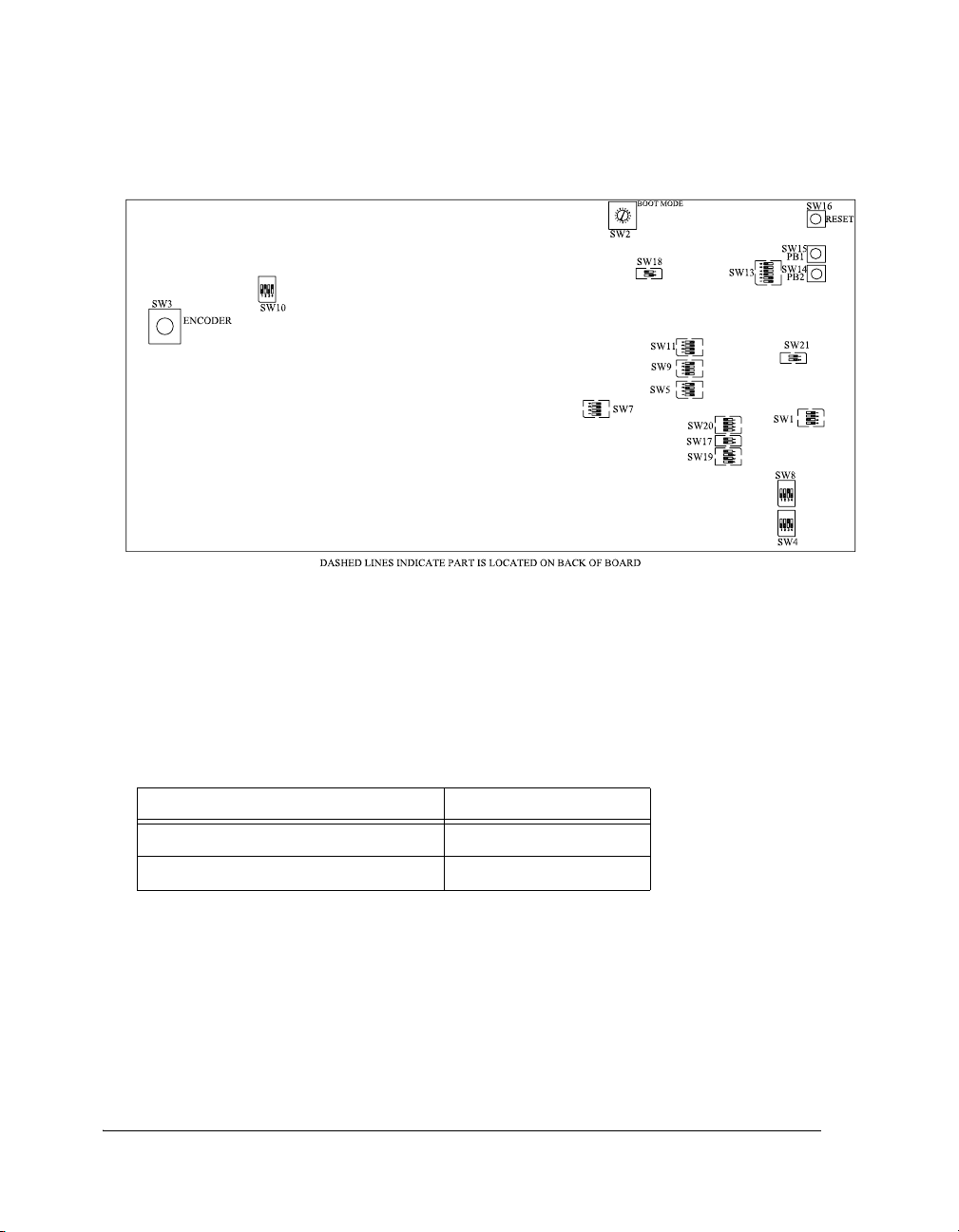
Push Button and Switch Settings
Figure 2-2. Push Button and Switch Locations
and 2 connect the management bus (
MDIO and MDC); SW1 position 3 enables
the 50 MHz RMII clock; and SW1 position 4 holds the PHY in reset (set to
OFF) or connects the PHY reset to the EZ-KIT Lite reset (set to ON).
Table 2-5. ETH Enable Switch (SW1)
SW1 Switch Setting Ethernet Mode
OFF, OFF, ON, OFF OFF (default)
ON, ON, OFF, ON ON
2-10 ADSP-BF527 EZ-KIT Lite Evaluation System Manual
Page 63

ADSP-BF527 EZ-KIT Lite Hardware Reference
Boot Mode Select Switch (SW2)
The rotary switch (SW2) determines the boot mode of the processor.
Table 2-6 shows the available boot mode settings. By default, the
ADSP-BF527 processor boots from the on-board parallel flash memory.
L
entire rotating portion of the switch, not the small arrow.
Table 2-6. Boot Mode Select Switch (SW2)
SW2 Position Processor Boot Mode
0 Reserved
1 Boot from 8-bit external flash memory (default)
2 Boot from 16-bit asynchronous FIFO
3 Boot from serial SPI memory
4 Boot from SPI host device
5 Boot from serial TWI memory
6 Boot from TWI host
7 Boot from UART0 host
8 Boot from UART1 host
9 Reserved
A Boot from SDRAM
B, C, D Reserved
The selected position of SW2 is marked by the notch down the
E Boot from 16-bit host DMA
F Boot from 8-bit host DMA
ADSP-BF527 EZ-KIT Lite Evaluation System Manual 2-11
Page 64

Push Button and Switch Settings
Rotary Encoder with Momentary Switch (SW3)
The rotary encoder (SW3) can be turned clockwise for an up count or
counter-clockwise for a down count. The encoder also features a momentary switch, activated by pushing down the switch and setting the counter
to zero. The rotary encoder is a two-bit quadrature (Gray code) encoder.
Refer to the “Rotary Counter” section of the ADSP-BF52x Hardware Ref-
erence Manual for additional information about interfacing with this style
rotary encoder.
The rotary encoder can be disconnected from the processor by setting the
rotary enable switch SW11 positions 1, 2 and 3 to OFF. See “Rotary NAND
Enable Switch (SW11)” on page 2-16 for more information.
MIC Gain Switch (SW4)
The microphone gain switch (SW4) sets the gain of the MIC signal, which
is connected to the top 3.5 mm jack (J7). The gain can be set to 14 dB,
0 dB, or –6 dB by turning ON position 1, 2 or 3 of the switch
(see Table 2-7). When the corresponding position for the desired gain is
ON, the remaining positions should be OFF. Refer to “Audio Interface” on
page 1-19 for more information on the audio codec.
Table 2-7. MIC Gain Switch (SW4)
Gain SW4 Switch Settings
5 (14 dB) ON, OFF, OFF, OFF
1 (0 dB) OFF, ON, OFF, OFF
0.5 (–6 dB) OFF, OFF, ON, OFF (default)
Unused OFF, OFF, OFF, OFF
2-12 ADSP-BF527 EZ-KIT Lite Evaluation System Manual
Page 65

ADSP-BF527 EZ-KIT Lite Hardware Reference
Keypad LCD Enable Switch (SW5)
The keypad LCD enable switch (SW5) connects the interrupt request signals PENIRQ and KEYIRQ to the MAX1233 keypad and touchscreen
controller (U16) on positions 1 and 2 (see Table 2-8). Positions 3 and 4 of
SW5 control the LCD reset line connection, selecting between GPIO (SW5
position 3 ON, position 4 OFF) or the board reset (SW5 position 3 OFF,
position 4 ON). Note that the GPIO reset line shares the pin with the
HOSTWR# and LED1 signals. The default setting is ON, ON, OFF, ON.
Table 2-8. Keypad LCD Enable Switch (SW5)
SW5 Position
(Default)
1 (ON)DSP
2 (ON)DSP
3 (OFF)DSP
4 (ON)RESET IC
From To Function
(U2, PF10)
(U2, PF9)
(U2, PG11)
(U27)
Keypad IC
(U16)
Keypad IC
(U16)
LCD conn
(P12)
LCD conn
(P12)
OFF (SW10.3 used as GPIO RTS of UART1, expan-
sion interface J2.31, J2.49, SPORT1 conn P7.7,
PPI conn
OFF (expansion interface pins: J2.33 J2.48,
SPORT1 conn P7.16, PPI conn P8.17)
ON (GPIO control of LCD_RESET),
OFF (host conn P13.4, LED1, expansion interface
J1.80, STAMP buffer U34.15)
OFF (LCD not connected to board reset)
P8.18)
Flash Enable Switch (SW7)
The flash enable switch (SW7) disconnects ~AMS signals from flash memory, allowing other devices to utilize the signals via the expansion
interface. For each switch listed in Table 2-9 that is turned
available flash memory is reduced by 1 MB.
OFF, the size of
ADSP-BF527 EZ-KIT Lite Evaluation System Manual 2-13
Page 66

Push Button and Switch Settings
Table 2-9. Flash Enable Switch (SW7)
SW7 Switch Position (Default) Processor Signal
1 (ON) ~AMS0
2 (ON) ~AMS1
3 (ON) ~AMS2
4 (ON) ~AMS3
Mic/HP LPBK Audio Mode Switch (SW8)
The SW8 switch allows the EZ-KIT Lite to be placed in loopback mode to
test for signal/circuit continuity and functionality (see “Power-On-Self
Test” on page 1-25). SW8 positions 1 and 2 connect the MICIN signal to the
headphone left and right outputs for audio loopback. Do not turn SW8
positions 1 and 2 ON at the same time.
SW8 positions 3 and 4 select the control interface for the audio codec.
SW8 position 3 ON and 4 OFF select SPI interface, while position 3 OFF and
position 4 ON select TWI mode. The SW8 default settings are OFF, OFF, ON,
OFF. See “SPI/TWI Switch (SW19)” on page 2-19 for more information.
2-14 ADSP-BF527 EZ-KIT Lite Evaluation System Manual
Page 67

ADSP-BF527 EZ-KIT Lite Hardware Reference
ETH Mode Flash CS Switch (SW9)
The Ethernet mode flash CS switch (SW9) sets the bootstrapping options
for the LAN8700 RMII PHY chip (U14). Table 2-10 shows the SW9 default
as well as the alternate switch settings.
SW9 position 4 disconnects SPISEL1 from the SPI flash chip (U8). Setting
SW9 position 4 OFF is useful when using SPISEL1 on the expansion inter-
face at connector J2 pin 11. SW9 default setting is position 4 ON.
Table 2-10. ETH Mode Flash CS Switch (SW9)
MODE[2:0] Setting Mode Definitions
111 All capable, auto negotiation (default)
110 Power down mode
101 Repeater mode, auto negotiation
100 100Base-TX half duplex advertised, auto negotiation
011 100Base-TX full duplex
010 100Base-TX half duplex
001 10Base-T full duplex
000 10Base-T half duplex
UART Enable Switch (SW10)
The UART enable switch (SW10) disconnects the UART1 signals from the
GPIO pins of the processor. When
can be used for other functions on the board.
ON. Flow control is not implemented in POST, so SW10 positions 1 and 3
are OFF. Refer to the ADM3202 datasheet for more information about the
UART interface.
ADSP-BF527 EZ-KIT Lite Evaluation System Manual 2-15
SW10 is OFF, its associated GPIO signals
SW10 default is OFF, ON, OFF,
Page 68

Push Button and Switch Settings
Rotary NAND Enable Switch (SW11)
The rotary NAND enable switch (SW11) disconnects the rotary encoder
signals from the GPIO pins of the processor. When SW11 is OFF, its associated GPIO signals can be used on the host interface (see Table 2-11).
Position 4 of SW11 disconnects the chip enable for NAND flash memory
(U4).
Table 2-11. Rotary NAND Enable Switch (SW11)
SW11 Position
(Default)
1 (ON)Encoder
2 (ON)Encoder
3 (ON)Encoder
4 (ON)DSP
From To Alternate Function/OFF Mode
SW3)
(
(SW3)
SW3)
(
(U2, PH10)
DSP
(U2, PF13)
DSP
(U2, PF12)
DSP
(U2, PF11)
NAND
(U4)
Expansion interface (
U34)
buffer (
CS audio codec (U2), CS keypad/touch controller
(U16), expansion interface (J2.30, J2.51),
STAMP buffer (U30)
Expansion interface (
U34)
buffer (
Host connector (P13.11), expansion interface
(J3.35)
J2.34, J2.52) STAMP
J2.32, J2.50), STAMP
GPIO Enable Switch (SW13)
The general-purpose input/output (GPIO) switch (SW13) disconnects the
associated push buttons and LED circuits from the GPIO pins of the processor and allows the signals to be used for other functions. Depending on
the switch configuration, the signals can be used as PPI clock select,
keypad_busy, or OTG host mode 5V select (see Table 2-12).
To select an on-board or external PPI clock through software, set
position 4
external expansion interface clock. Drive
PPI oscillator. By default, SW13 position 4 is OFF and the PPI clock source
is on-board.
ON. Drive the PG12 programmable flag to low (0) to connect an
PG12 high to select the on-board
SW13
2-16 ADSP-BF527 EZ-KIT Lite Evaluation System Manual
Page 69

ADSP-BF527 EZ-KIT Lite Hardware Reference
Table 2-12. GPIO Enable Switch (SW13)
SW13 Position
(Default)
1 (ON)Push
2 (ON)Push
3 (OFF)NC
4 (OFF)DSP
5 (OFF) Keypad BUSY
6 (OFF)OTG PWR
The
USB_VRSEL signal is used to provide 5V to a device connected over the
From To Function
button 1
button 2
(U2, PG12)
(U16)
VR3, U28)
(
DSP
(U2, PG0)
DSP
(U2, PG13)
PPI CLK
(U20)
DSP
(U2, PG0)
DSP
(U2, PG13)
ON (PB1), OFF (UART1 CTS U25, host connector
P13.12, keypad busy SW13.8, expansion interface
J1.84)
ON (PB2), OFF (host connector P13.8, OTG volt-
age select SW13.7, expansion interface J1.85)
OFF (LED2, host connector P13.10, expansion
interface J1.81, STAMP buffer U34), ON (PPI
U20)
CLK
OFF (PB1, UART1 CTS U25, host conn P13.12,
expansion interface J1.84), ON (GPIO
keypad busy U16, SW13.1)
OFF (host connector P13.8, expansion interface
J1.85), ON (PB2 SW13.11, OTG power VR3, U28)
USB OTG interface when running in host mode. Signal USB_VRSEL is connected by setting SW13 position 2 OFF and position 6 ON. Then the PG13
programmable flag pin of the processor can be used to control the 5V regulator (VR3). Refer to “USB OTG Interface” on page 1-20 for more
information.
The PG0 PF pin of the processor can be used as GPIO or other functions if
SW13 position 1 is turned OFF. Turning SW13 position 1 OFF and position 5
ON allows the keypad_busy signal to connect to the processor from the key-
pad and touchscreen controller (U16). SW13 default settings are ON, ON, OFF,
OFF, OFF, OFF.
ADSP-BF527 EZ-KIT Lite Evaluation System Manual 2-17
Page 70

Push Button and Switch Settings
Programmable Flag Push Buttons (SW14–15)
Two momentary push buttons (SW14–15) are provided for general-purpose
user input. The buttons connect to the PG0 and PG13 GPIO pins of the
processor. The push buttons are active high and, when pressed, send a
high (1) to the processor. The GPIO enable switch (SW13) disconnects the
push buttons from the corresponding PB signal. Refer to “GPIO Enable
Switch (SW13)” on page 2-16 for more information.
Reset Push Button (SW16)
The reset push button (SW16) resets the following ICs.
• processor (U2), parallel flash (U5), PHY (U14) if SW1 position 4 is ON
•LCD (P12) if SW5 position 3 is OFF and 4 is ON
•CPLD (U33)
The reset push button does not reset the following ICs.
•SDRAM (U7), NAND flash (U4), SPI flash (U8)
• audio codec (U2), keypad/touchscreen controller (U16)
• UART1 (U25)
The reset push button does not reset the debug agent once it has been
connected to a PC. The USB chip is not reset when the push button is
pressed after the USB cable has been plugged in and communication with
the PC has been initialized correctly. After USB communication has been
initialized, the only way to reset the USB chip is by powering down the
board.
2-18 ADSP-BF527 EZ-KIT Lite Evaluation System Manual
Page 71

ADSP-BF527 EZ-KIT Lite Hardware Reference
SPORT0A ENBL Switches (SW17 and SW20)
The SPORT0A enable switches (SW17 and SW20) connect the SPORT0A interface of the processor to the audio codec. When the SPORT0A interface is
needed at the expansion interface, turn SW17 and SW20 all OFF. The SW17 or
SW20 switches are all ON by default.
KEY/PEN CS Switch (SW18)
The KEY/PEN CS switch (SW18) enables the chip select for the MAX1233
touchscreen controller to be connected to either signal: SPISEL2 (ON, OFF)
or SPISEL4 (OFF, ON). SPISEL4 is one function on a multiplexed pin of PF
PH8. When using the PH8 programmable flag pin as SPISEL4, signals ERXD1
and HOSTD8 do not operate as Ethernet and host data pins.
SPI/TWI Switch (SW19)
The SPI/TWI switch (SW19) selects the control interface for the audio
codec. SW19 default is ON, OFF, ON, OFF, which selects SPI interface. TWI is
selected by setting the SW19 switch to OFF, ON, OFF, ON. See “Mic/HP LPBK
Audio Mode Switch (SW8)” on page 2-14 for more information on how
to setup the audio mode.
TFS0A/HOSTCE Enable Switch (SW21)
The TFS0A/HOSTCE enable switch (SW21) disconnects the PG15 programmable flag signal TFS0A_RMIIMDINT#_HOSTCE# from the SPORT0 (position 1)
connector
OFF, OFF by default.
ADSP-BF527 EZ-KIT Lite Evaluation System Manual 2-19
P6 pin 11 and the host connector (position 2) P13 pin 6. SW21 is
Page 72

Jumpers
Jumpers
This section describes functionality of the configuration jumpers.
Figure 2-3 shows the locations of the configuration jumpers.
Figure 2-3. Configuration Jumper Locations
HWAIT Enable Jumper (JP1)
The HWAIT enable jumper (JP1) connects processor signal
HWAIT_PUSHBUTTON1, PF PG0, to SW10 position 1. SW10 position 1 then con-
nects to the transmit 2 input of the UART1 IC (U25). This allows the
implementation of flow control functionality
of the processor. Install JP1 if implementing flow control. JP1 is uninstalled by default.
2-20 ADSP-BF527 EZ-KIT Lite Evaluation System Manual
CTS through the HWAIT signal
Page 73

ADSP-BF527 EZ-KIT Lite Hardware Reference
LCD PPI Jumper (JP2)
The PPI port connects to the LCD through two buffers (U31–32). JP2
enables both buffers when installed and drives PPI signals to LCD connector (P12). Removing JP2 is useful when using the PPI at the PPI connector
(P8) or expansion interface. JP2 is installed by default.
STAMP Enable Jumper (JP3)
The STAMP connectors have a number of nets connected by enabling
quick switches at locations U30 and U34. When installed, the STAMP
enable jumper (JP3) enables the quick switches. Table 2-13 lists the signals that are connected when JP3 is installed. JP3 is uninstalled by default.
Table 2-13. UART1 Loopback Jumper (JP5)
STAMP Signals Connected through Quick Switches U30 and U34
SCL DR0PRIA
SDA RFS0A
SPISCK CZM
SPISEL1 CUD
SPISEL2#_CDG LED0
SPIMISO HOSTWR#_LED1
SPIMOSI HOSTACK_LED2
RSCLK0A
ADSP-BF527 EZ-KIT Lite Evaluation System Manual 2-21
Page 74

Jumpers
UART1 Loopback Jumper (JP5)
The UART1 loopback jumper (JP5) is used to place the UART1 port of the
processor in a loopback condition. The jumper connects the UART1_TX line
of the processor to the UART1_RX signal of the processor. The jumper is
required when the power-on-self-test (POST) is run to test the serial port
interface. The default setting is uninstalled.
MIC Select Jumper (JP6)
The MIC select jumper (JP6) connects the MICBIAS signal to the MICIN
(JP6 on 1 and 2) or connects MICBIAS to the 3.5 mm connector J7 (JP6 on
2 and 3). The default setting is JP6 installed on 2 and 3.
VDDINT Power Jumper (P14)
The VDDINT power jumper (P14) is used to measure the core voltage and
current supplied to the processor core. P14 is ON by default, and the power
flows through the two-pin IDC header. To measure power, remove the
jumper and measure the voltage across the 0.05 ohm resistor. Once the
voltage is measured, the power can be calculated. For more information,
refer to “Power Measurements” on page 1-25.
VDDEXT Power Jumper (P15)
The VDDEXT power jumper (P15) is used to measure the processor’s I/O
voltage and current. JP15 is ON by default, and the power flows through
the two-pin IDC header. To measure power, remove the jumper and measure the voltage across the 0.05 ohm resistor. Once the voltage is
measured, the power can be calculated.
2-22 ADSP-BF527 EZ-KIT Lite Evaluation System Manual
Page 75
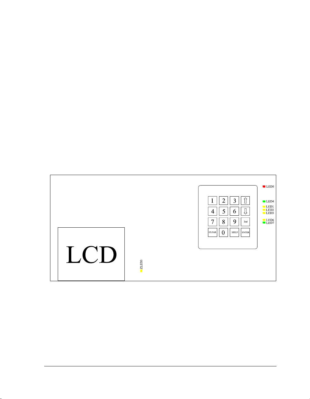
ADSP-BF527 EZ-KIT Lite Hardware Reference
VDDMEM Power Jumper (P16)
The VDDMEM power jumper (P16) is used to measure the voltage and current
supplied to the memory interface of the processor. P16 is ON by default,
and the power flows through the two-pin IDC header. To measure power,
remove the jumper and measure the voltage across the 0.05 ohm resistor.
Once the voltage is measured, the power can be calculated.
LEDs
This section describes the on-board LEDs. Figure 2-3 shows the LED
locations.
Figure 2-4. LED Locations
ADSP-BF527 EZ-KIT Lite Evaluation System Manual 2-23
Page 76

LEDs
User LEDs (LED1–3)
Three LEDs connect to three general-purpose I/O pins of the processor
(see Table 2-14). The LEDs are active high and are lit by writing a 1 to the
correct PF signal.
Table 2-14. User LEDs
LED Reference Designator Processor Programmable Flag Pin
LED1 PF8
LED2 PG11
LED3 PG12
Power LED (LED4)
When LED4 is lit (green), it indicates that power is being properly supplied
to the board.
Reset LED (LED5)
When LED5 is lit, it indicates that the master reset of all major ICs is
active. The reset LED is controlled by the Analog Devices ADM708
supervisory reset circuit. You can assert the reset push button (SW16) to
assert the master reset and to activate
LED5. For more information, see
“Reset Push Button (SW16)” on page 2-18.
Ethernet LEDs (LED6–7)
When LED6 is lit solid, it indicates that the SMSC LAN8700 chip (U14)
detects a valid link. When transmit or receive activity is sensed,
flashes as an activity indicator. For more information on the LEDs, refer
to the LAN8700 chip datasheet provided by the product manufacturer.
2-24 ADSP-BF527 EZ-KIT Lite Evaluation System Manual
LED7
Page 77
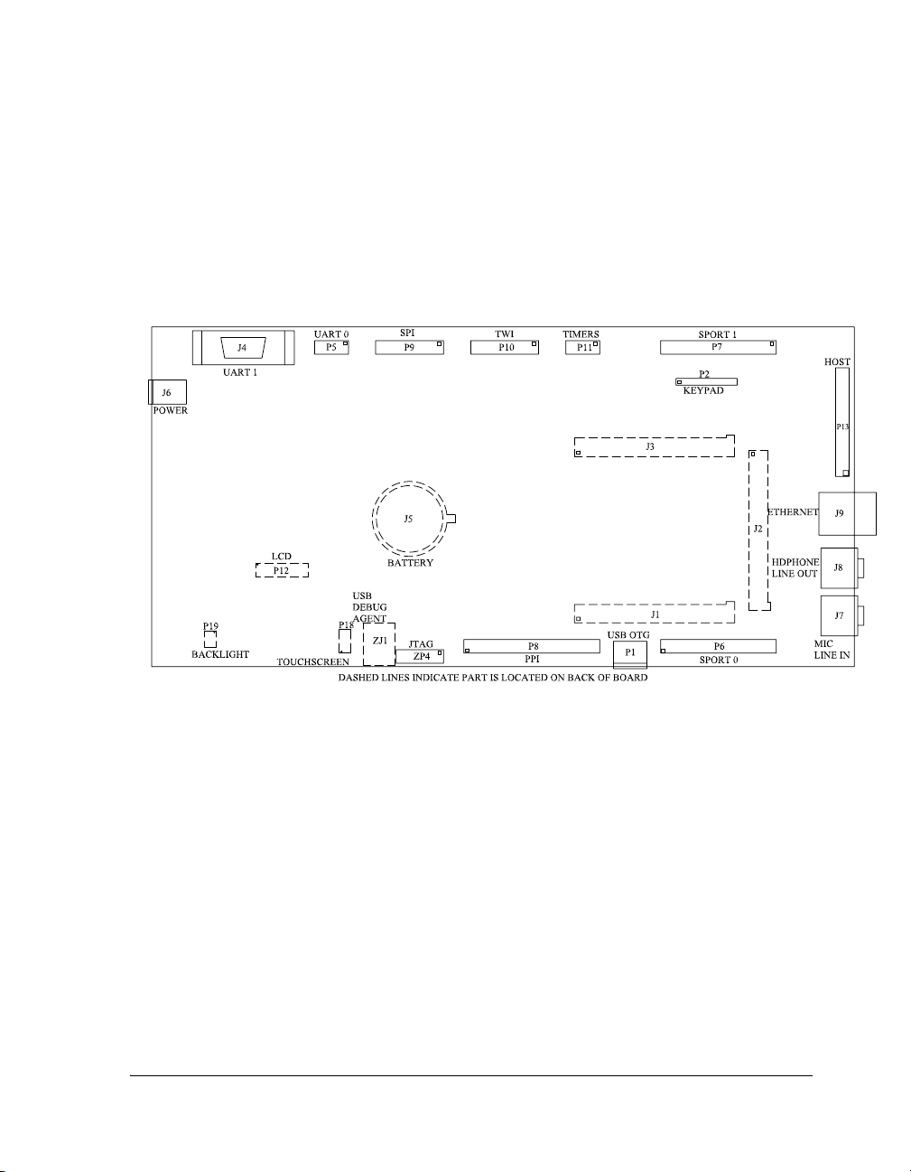
ADSP-BF527 EZ-KIT Lite Hardware Reference
Connectors
This section describes connector functionality and provides information
about mating connectors. The connector locations are shown in
Figure 2-5.
Figure 2-5. Connector Locations
ADSP-BF527 EZ-KIT Lite Evaluation System Manual 2-25
Page 78

Connectors
Expansion Interface Connectors (J1–3)
Three board-to-board connector footprints provide signals for most of the
processor’s peripheral interfaces. The connectors are located at the bottom
of the board. For more information, see “Expansion Interface” on
page 1-24. For the availability and pricing of the J1–3 connectors, contact
Samtec.
Part Description Manufacturer Part Number
90-position 0.05” spacing, SMT SAMTEC SFC-145-T2-F-D-A
Mating Connector
90-position 0.05” spacing
(through hole)
90-position 0.05” spacing
(surface mount)
90-position 0.05” spacing
(low cost)
SAMTEC TFM-145-x1 series
SAMTEC TFM-145-x2 series
SAMTEC TFC-145 series
2-26 ADSP-BF527 EZ-KIT Lite Evaluation System Manual
Page 79

ADSP-BF527 EZ-KIT Lite Hardware Reference
RS-232 Connector (J4)
Part Description Manufacturer Part Number
DB9, female, vertical mount NORCOMP 191-009-213-L-571
Mating Cable
2m female-to-female cable DIGI-KEY AE1020-ND
Battery Holder (J5)
Part Description Manufacturer Part Number
24 mm battery holder KEYSTONE 105
Mating Battery (shipped with EZ-KIT Lite)
3V 280MAH 24 mm LI-COIN SANYO CR2430
Power Connector (J6)
The power connector (J6) provides all of the power necessary to operate
the EZ-KIT Lite board.
Part Description Manufacturer Part Number
2.5 mm power jack SWITCHCRAFT RAPC712X
Mating Power Supply (shipped with EZ-KIT Lite)
7.0VDC@2.14A power supply CUI INC DMS070214-P6P-SZ
ADSP-BF527 EZ-KIT Lite Evaluation System Manual 2-27
Page 80

Connectors
Dual Audio Connectors (J7–8)
Part Description Manufacturer Part Number
3.5 mm dual stereo jack SWITCHCRAFT 35RAPC7JS
Mating Cable (shipped with EZ-KIT Lite)
3.5 mm male/male 6’ cable RANDOM 10A3-01106
Mating Headphone (shipped with EZ-KIT Lite)
3.5 mm stereo headphones KOSS 151225 UR5
Ethernet Connector (J9)
Part Description Manufacturer Part Number
RJ-45 Ethernet jack STEWART SS-6488-NF
Mating Cable (shipped with EZ-KIT Lite)
Cat 5E patch cable RANDOM PC10/100T-007
USB OTG Connector (P1)
The pinout of the P1 connector can be found in “ADSP-BF527 EZ-KIT
Lite Schematic” on page B-1.
Part Description Manufacturer Part Number
USB 5-pin mini AB MOLEX 56579-0576
Mating Cables (shipped with EZ-KIT Lite)
5-in-1 USB 2.0 cable JO-DAN INTERNAT GXQU-06
2-28 ADSP-BF527 EZ-KIT Lite Evaluation System Manual
Page 81

ADSP-BF527 EZ-KIT Lite Hardware Reference
Keypad Connector (P2)
Part Description Manufacturer Part Number
IDC header female SAMTEC SSW-109-01-TM-S
Mating Keypad (shipped with EZ-KIT Lite)
4 x 4 keypad ACT COMPONENTS ACT-07-30008-000-R
VPP Board Connector (P4)
The VPP board connector (P4) is not populated and is for testing purposes
only, not intended for use.
UART0 Connector (P5)
The pinout of the P5 connector can be found in “ADSP-BF527 EZ-KIT
Lite Schematic” on page B-1.
Part Description Manufacturer Part Number
IDC header FCI 68737-410HLF
Mating Connector
IDC socket DIGI-KEY S4205-ND
ADSP-BF527 EZ-KIT Lite Evaluation System Manual 2-29
Page 82

Connectors
SPORT0 Connector (P6)
The pinout of the P6 connector can be found in “ADSP-BF527 EZ-KIT
Lite Schematic” on page B-1.
Part Description Manufacturer Part Number
IDC header FCI 68737-434HLF
Mating Connector
IDC socket DIGI-KEY S4217-ND
SPORT1 Connector (P7)
The pinout of the P7 connector can be found in “ADSP-BF527 EZ-KIT
Lite Schematic” on page B-1.
Part Description Manufacturer Part Number
IDC header FCI 68737-434HLF
Mating Connector
IDC socket DIGI-KEY S4217-ND
PPI Connector (P8)
The pinout of the P8 connector can be found in “ADSP-BF527 EZ-KIT
Lite Schematic” on page B-1.
Part Description Manufacturer Part Number
IDC header FCI 68737-440HLF
Mating Connector
IDC socket DIGI-KEY S4220-ND
2-30 ADSP-BF527 EZ-KIT Lite Evaluation System Manual
Page 83

ADSP-BF527 EZ-KIT Lite Hardware Reference
SPI Connector (P9)
The pinout of the P9 connector can be found in “ADSP-BF527 EZ-KIT
Lite Schematic” on page B-1.
Part Description Manufacturer Part Number
IDC header FCI 68737-420HLF
Mating Connector
IDC socket DIGI-KEY S4210-ND
Two-Wire Interface Connector (P10)
The pinout of the P10 connector can be found in “ADSP-BF527 EZ-KIT
Lite Schematic” on page B-1.
Part Description Manufacturer Part Number
IDC header FCI 68737-420HLF
Mating Connector
IDC socket DIGI-KEY S4210-ND
TIMERS Connector (P11)
The pinout of the P11 connector can be found in “ADSP-BF527 EZ-KIT
Lite Schematic” on page B-1.
Part Description Manufacturer Part Number
IDC header FCI 68737-410HLF
Mating Connector
IDC socket DIGI-KEY S4205-ND
ADSP-BF527 EZ-KIT Lite Evaluation System Manual 2-31
Page 84

Connectors
LCD Data Connector (P12)
Part Description Manufacturer Part Number
FPC 16-pin 1 mm HIROSE FH12-16S-1SH(55)
Mating LCD Display Module (shipped with EZ-KIT Lite)
3.5” TFT LCD with touchscreen Varitronix COG-T350MCQB-01
Host Interface Connector (P13)
The pinout of the P13 connector can be found in “ADSP-BF527 EZ-KIT
Lite Schematic” on page B-1.
Part Description Manufacturer Part Number
IDC header SAMTEC TSW-116-26-T-D
Mating Connector
IDC socket SAMTEC TSW-116-01-T-D
CPLD JTAG Connector (P17)
The CPLD JTAG connector (P17) is not populated; the CPLD code
should not be altered for LCD operations.
Part Description Manufacturer Part Number
IDC header FCI 68737-410HLF
Mating Connector
IDC socket DIGI-KEY S4205-ND
2-32 ADSP-BF527 EZ-KIT Lite Evaluation System Manual
Page 85

ADSP-BF527 EZ-KIT Lite Hardware Reference
LCD Touchscreen Connector (P18)
There is no connector for the touchscreen; the flex cable is soldered
directly to the board.
LCD Backlight Connector (P19)
There is no connector for the backlight; the flex cable is soldered directly
to the board.
USB Debug Agent Connector (ZJ1)
The USB debug agent connector is the connecting point for the JTAG
USB debug agent interface. The JTAG header (ZP4) should not be used
whenever ZJ1 and its mating cable are used to communicate to the processor via VisualDSP++.
JTAG Connector (ZP4)
The JTAG header is the connecting point for a JTAG in-circuit emulator
pod. When an emulator connects to the JTAG header, the USB debug
interface is disabled.
Pin 3 is missing to provide keying. Pin 3 in the mating connector should
have a plug.
When using an emulator with the EZ-KIT Lite board, follow the connection instructions provided with the emulator.
ADSP-BF527 EZ-KIT Lite Evaluation System Manual 2-33
Page 86

Connectors
2-34 ADSP-BF527 EZ-KIT Lite Evaluation System Manual
Page 87

A B C
D
1
1
2
2
ADSP-BF527 EZ-KIT LITE
SCHEMATIC
3
ANALOG
4
DEVICES
20 Cotton Road
Nashua, NH 03063
PH: 1-800-ANALOGD
3
4
Title
ADSP-527 EZ-KIT Lite
TITLE
Size Board No.
C
Date Sheet of
A B C D
A0208-2006
Rev
1.4
1 1311-12-2007_14:00
Page 88

A B C
D
3.3V
R89
TP3
A[1:19]
1
SCKE
TP2
SWE
SA10
SCAS
SRAS
SMS
RESET
2
3.3V
R3
R29
10K
0402
DNP
R34
10K
0402
10K
0402
R5
10K
0402
DNP
R196
10K
0402
A1
A2
A3
A4
A5
A6
A7
A8
A9
A10
A11
A12
A13
A14
A15
A16
A17
A18
A19
3
U2
AB8
A1
AC8
A2
AB7
A3
AC7
A4
AC6
A5
AB6
A6
AB4
A7
AB5 T1
A8 D7
AC5
A9
AC4
A10
AB3
A11
AC3
A12
AB2
A13
AC2
A14
AA2
A15
W2
A16
Y2
A17
AA1
A18
AB1
A19
AB13
SCKE
AB10
SWE
AC10
SA10
AC11
SCAS
AB12
SRAS
AC13
SMS
T22
GND54
U22
NMI
AB22
VRSEL
V22 AB19
RESET CLKBUF
ADSP-BF527
MBGA289
ABE1#/SDQM1
ABE0#/SDQM0
WAKEUP_OUT
D0
D1
D2
D3
D4
D5
D6
D8
D9
D10
D11
D12
D13
D14
D15
AMS3
AMS2
AMS1
AMS0
AOE
ARE
AWE
ARDY
CLKOUT
VROUT
SS/PG
Y1
V2
W1
U2
V1
U1
T2
R1
P1
P2
R2
N1
N2
M2
M1
AC9
AB9
AB15
AC16
AB16
AC17
AC15
AB17
AB14
AC14
AB18
AC18
AC20
AC19
D0
D1
D2
D3
D4
D5
D6
D7
D8
D9
D10
D11
D12
D13
D14
D15
TP13
TP1
ABE1#/SDQM1
ABE0#/SDQM0
AMS3
AMS2
AMS1
AMS0
AOE
ARE
AWE
ARDY
VREFFLT
D[0:15]
VROUT
R9
33
0402
R4
0
0402
DNP
SPISCK
CLKOUT
CLKBUF
MDC_HOSTRD#
3.3V
TDO
UART1RTS_PENIRQ#
SPISEL2#_CDG
R8
33
0402
R10
33
0402
HWAIT_PUSHBUTTON1
DT0PRIA_PPIFS3
HOSTWR#_LED1
HOSTACK_LED2
HOSTADDR_PUSHBUTTON2
TFS0A_RMIIMDINT#_HOSTCE#
R192
0
0402
DSP_CLKIN
DSP_RTXI
DSP_RTXO
PPID0
PPID1
PPID2
PPID3
PPID4
PPID5
PPID6
PPID7
LED0
KEYIRQ#
CZM
CUD
UART1TX
UART1RX
SPISEL1
SPIMISO
SPIMOSI
PPIFS2
DR0PRIA
RFS0A
RSCLK0A
TSCLK0A
TRST
TMS
EMU
TCK
TDI
U2
R23
XTALI
P23
XTALO
U23 C22
RTXI PJ3/SDA
V23
RTXO
A7
PF0/PPID0/DR0PRI/ND_D0A
B8
PF1/PPID1/RFS0/ND_D1A
A8
PF2/PPID2/RSCLK0/ND_D2A
B9
PF3/PPID3/DT0PRI/ND_D3A
B11
PF4/PPID4/TFS0/ND_D4A/TACLK0
B10
PF5/PPID5/TSCLK0/ND_D5A/TACLK1
B12
PF6/PPID6/DT0SEC/ND_D6A/TACI0
B13
PF7/PPID7/DR0SEC/ND_D7A/TACI1
B16
PF8/PPID8/DR1PRI
A20
PF9/PPID9/RSCLK1/SPISEL6#
B15
PF10/PPID10/RFS1/SPISEL7#
B17
PF11/PPID11/TFS1/CZM
B18
PF12/PPID12/DT1PRI/SPISEL2#/CDG
B19
PF13/PPID13/TSCLK1/SPISEL3#/CUD
A9
PF14/PPID14/DT1SEC/UART1TX
A10
PF15/PPID15/DR1SEC/UART1RX/TACI3
H2
PG0/HWAIT
G1
PG1/SPISS#/SPISEL1#
H1
PG2/SPISCK
F1
PG3/SPIMISO/DR0SECA
D1
PG4/SPIMOSI/DT0SECA
D2
PG5/TMR1/PPIFS2/TFS0A
C2
PG6/DT0PRIA/TMR2/PPIFS3
B1
PG7/TMR3/DR0PRIA/UART0TX
C1
PG8/TMR4/RFS0A/UART0RX/TACI4
B2
PG9/TMR5/RSCLK0A/TACI5
B4
PG10/TMR6/TSCLK0A/TACI6
B3
PG11/TMR7/HOST_WR#
A2
PG12/DMAR1/UART1TXA/HOST_ACK
A3
PG13/DMAR0/UART1RXA/HOST_ADDR/TACI2
A4
PG14/TSCLK0A1/MDC/HOST_RD#
A5
PG15/TFS0A/MIIPHYINT#/RMIIMDINT#/HOST_CE#
K2
TRST
L2
TMS
J2
EMU
L1
TCK
K1
TDO
J1
TDI
ADSP-BF527
MBGA289
PH0/ND_D0/MIICRS/RMIICRSDV/HOST_D0
PH1/ND_D1/ERXER/HOST_D1
PH2/ND_D2/MDIO/HOST_D2
PH3/ND_D3/ETXEN/HOST_D3
PH4/ND_D4/MIITXCLK/RMIIREF_CLK/HOST_D4
PH5/ND_D5/ETXD0/HOST_D5
PH6/ND_D6/ERXD0/HOST_D6
PH7/ND_D7/ETXD1/HOST_D7
PH8/SPISEL4#/ERXD1/HOST_D8/TACLK2
PH9/SPISEL5#/ETXD2/HOST_D9/TACLK3
PH10/ND_CE#/ERXD2/HOST_D10
PH11/ND_WE/ETXD3/HOST_D11
PH12/ND_RE/ERXD3/HOST_D12
PH13/ND_BUSY/ERXCLK/HOST_D13
PH14/ND_CLE/ERXDV/HOST_D14
PH15/ND_ALE/COL/HOST_D15
PJ0/PPIFS1/TMR0
PJ1/PPICLK/TMRCLK
PJ2/SCL
BMODE0
BMODE1
BMODE2
BMODE3
B7
A6
B22
A11
A12
A13
B14
A14
K23
K22
L23
L22
T23
M22
R22
M23
N22
N23
P22
G2
F2
E1
E2
R14
10K
0402
PPIFS1
SCL
SDA
NDD0_RMIICRSDV_HOSTD0
NDD1_ERXER_HOSTD1
NDD2_MDIO_HOSTD2
NDD3_ETXEN_HOSTD3
NDD5_ETXD0_HOSTD5
NDD6_ERXD0_HOSTD6
NDD7_ETXD1_HOSTD7
ERXD1_HOSTD8
SPISEL5#_HOSTD9
NDCE#_HOSTD10
NDWR#_HOSTD11
NDRE#_HOSTD12
NDBUSY#_HOSTD13
NDCLE_HOSTD14
NDALE_HOSTD15
R11
10K
04020402
10K
R7
33
0402
"BOOT MODE"
R13R12
10K
0402
ARDY
R6
0
0402
SW2
1
2
7
8
4
9
8
SWT023
ROTARY
6
A
5
BCD
10K
0402
PPICLK
NDD4_RMIIREFCLK_HOSTD4
4
3
2
1
0
F
E
R87
1.2K
0402
3.3V
C
R88
1.2K
0402
1
2
3
SW2: Boot Mode Select Switch
3.3V
R2
10K
0402
4
3.3V
4
C2
0.01UF
0402
U3
VDD
1 3
OE OUT
GND
2
25MHZ
OSC003
R1
33
0402
DSP_CLKIN
DSP_RTXI DSP_RTXO
R15
10M
0603
U1
C3
18PF
0805
1
TERM1 TERM2
2
NC1 NC2
32.768KHZ
OSC008
4
3
C1
18PF
0805
RTC
VREFFLT
R147
100K
0402
DNP
R138
33.0K
0402
DNP
C95
220PF
0402
DNP
Default
0
1
2
3
4
5
6
7
8
9
A
B
C
D
E
F
U3
BOOT MODEPOSITION
Reserved
Boot from 8 or 16-bit external flash memory
Boot from 16-bit asynchronous FIFO
Boot from serial SPI memory
Boot from SPI host device
Boot from serial TWI memory
Boot from TWI host
Boot from UART0 host
Boot from UART1Host
Reserved
Boot from SDRAM
Reserved
Reserved
Reserved
Boot from 16-Bit Host DMA
Boot from 8-Bit Host DMA
ANALOG
20 Cotton Road
Nashua, NH 03063
PH: 1-800-ANALOGD
Title
DEVICES
ADSP-527 EZ-KIT Lite
DSP EBIU + CONTROL
Size Board No.
C
Date Sheet of
A0208-2006
4
Rev
1.4
13211-13-2007_14:44
A B C D
Page 89

A B C
D
VDDEXT
U2
G7
VDDEXT1
G8
VDDEXT2
G9
VDDEXT3
G10
VDDEXT4
G11
VDDEXT5
G12
VDDEXT6
G13
VDDEXT7
G14
VDDEXT8
1
VDDMEM
2
VDDINT
3
"RTC BATTERY"
VDDEXT
D1
MA3X717E
DIO005
4
J5
CON054
BATTHOLDER
12
C4
0.01UF
0402
G15
VDDEXT9
H7
VDDEXT10
J17
VDDEXT11
K17
VDDEXT12
L17
VDDEXT13
M17
VDDEXT14
N17
VDDEXT15
P17
VDDEXT16
R17
VDDEXT17
J7
VDDMEM1
K7
VDDMEM2
L7
VDDMEM3
M7
VDDMEM4
N7
VDDMEM5
P7
VDDMEM6
R7
VDDMEM7
T7
VDDMEM8
U7
VDDMEM9
U8
VDDMEM10
U9
VDDMEM11
U10
VDDMEM12
U11
VDDMEM13
U12
VDDMEM14
U13
VDDMEM15
U14
VDDMEM16
U15
VDDMEM17
U16
VDDMEM18
B5
VDDINT1
H8
VDDINT2
H9
VDDINT3
H10
VDDINT4
H11
VDDINT5
H12
VDDINT6
H13
VDDINT7
H14
VDDINT8
H15
VDDINT9
H16
VDDINT10
J8
VDDINT11
J16
VDDINT12
K8
VDDINT13
K16
VDDINT14
L8
VDDINT15
L16
VDDINT16
M8
VDDINT17
M16
VDDINT18
N8
VDDINT19
N16
VDDINT20
P8
VDDINT21
P16
VDDINT22
R8
VDDINT23
R16
VDDINT24
T8
VDDINT25
T9
VDDINT26
T10
VDDINT27
T11
VDDINT28
T12
VDDINT29
T13
VDDINT30
T14
VDDINT31
T15
VDDINT32
T16
VDDINT33
W23
VDDRTC
ADSP-BF527
MBGA289
EVDD_VREG
EVDD_VREG_N
AVDD_OTP
OTP_VPP
GND1
GND2
GND3
GND4
GND5
GND6
GND7
GND8
GND9
GND10
GND11
GND12
GND13
GND14
GND15
GND16
GND17
GND18
GND19
GND20
GND21
GND22
GND23
GND24
GND25
GND26
GND27
GND28
GND29
GND30
GND31
GND32
GND33
GND34
GND35
GND36
GND37
GND38
GND39
GND40
GND41
GND42
GND43
GND44
GND45
GND46
GND47
GND48
GND49
GND50
GND51
GND52
GND53
A1
A23
AC1
AC23
B6
J9
J10
J11
J12
J13
J14
K9
K10
K11
K12
K13
K14
K15
L9
L10
L11
L12
L13
L14
L15
M9
M10
M11
M12
M13
M14
M15
N9
N10
N11
N12
N13
N14
N15
P9
P10
P11
P12
P13
P14
P15
R9
R10
R11
R12
R13
R14
R15
T17
U17
AC12
AB11
R56
0
0402
C111
0.1UF
0402
R35
0
0402
C146
0.1UF
0402
3.3V 2.5V
R49
0
0402
C136
0.1UF
0402
C135
0.1UF
0402
R180
0
0402
STAMP_LED0
VDDEXT
C68
10UF
VDDEXT
C59
10UF
VDDINT
C33
10UF
VDDINT
C22
10UF
VDDINT
C7
10UF
VDDMEM
C52 C50
10UF
0.1UF
0402
P4
1
2
3
4
5
6
7
8
IDC8X1_SMT
DNP
0.1UF
0402
0.1UF
0402
0.1UF
0402
0.1UF
0402
C43
10UF
0805
C65
0.1UF
0402
C56
0.1UF
0402
C29
0.1UF
0402
C18
0.1UF
0402
C13
0.1UF
0402
0.1UF
0402
C64
0.1UF
0402
C61 C60
0.01UF
0402
C28
0.1UF
0402
C17
0.1UF
0402
C14
0.1UF
0402
C49
0.1UF
0402
C70 C69
0.01UF
0402
0.01UF
04020805
C27
0.1UF
0402
C16
0.1UF
0402
C15
0.1UF
0402
C48
0.1UF
0402
0.01UF
04020805
C62
0.01UF
C35 C34
0.01UF
0402
C24 C23
0.01UF
0402
C9 C8
0.01UF
0402
C47
0.1UF
0402
C71
0.01UF
C58C57
0.01UF
0402
0.01UF
04020805
0.01UF
04020805
0.01UF
04020805
C41
0.1UF
0402
C67C66
0.01UF
0402
C63
0.01UF
04020402
C36
0.01UF
C25
0.01UF
C10
0.01UF
0.1UF
0402
C72
0.01UF
04020402
C32
0.01UF
0402
C21
0.01UF
0402
C6
0.01UF
0402
C39
0.1UF
0402
C37
0.01UF
04020402
C26
0.01UF
04020402
C11
0.01UF
04020402
C38
0.1UF
04020805
C31C30
0.01UF
0402
C20C19
0.01UF
0402
C5C12
0.01UF
0402
C54 C53
0.01UF
0402
Title
C55
0.01UF
0402 0402
0.01UF
0402
C51
0.01UF
ANALOG
DEVICES
ADSP-527 EZ-KIT Lite
DSP POWER
C45 C44
0.01UF
0402
0.01UF
0402 0402
20 Cotton Road
Nashua, NH 03063
PH: 1-800-ANALOGD
C46
0.01UF
0402
C42C40
0.01UF
1
2
3
4
Size Board No.
"VPP BOARD"
C
Date Sheet of
11-29-2007_11:52 133
A B C D
A0208-2006
Rev
1.4
Page 90
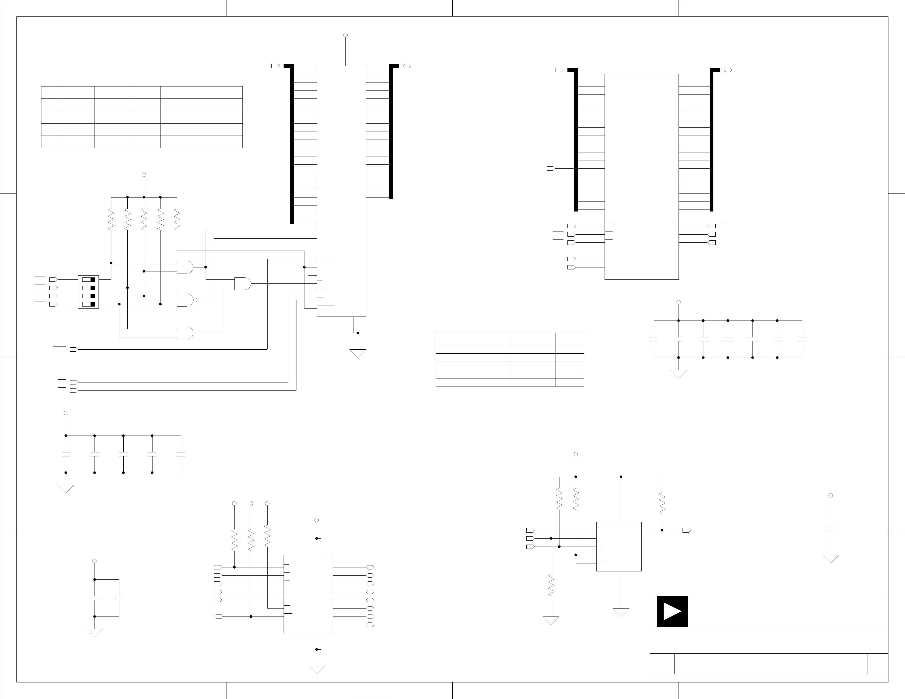
A B C
D
4 MB FLASH
(2M x 16)
A[1:19]
SW7: FLASH Enable
FROM DEFAULTTO ALTERNATE FUNCTION / OFF MODEPOS.
SW7.1
DSP (U2)
FLASH (U5)
1
SW7.2
SW7.3
SW7.4
DSP (U2)
DSP (U2)
DSP (U2)
FLASH (U5)
FLASH (U5)
FLASH (U5)
R20 R19
10K
0402
ON
ON
ON
ON
3.3V
R18 R17
10K
10K
0402 0402
J2.65 (Expansion Interface)
J2.63 (Expansion Interface)
J2.61 (Expansion Interface)
J2.59 (Expansion Interface)
R16
10K
10K
0402
0402
A1
A2
A3
A4
A5
A6
A7
A8
A9
A10
A11
A12
A13
A14
A15
A16
A17
A18
A19
G2
F2
E2
C2
D2
F3
E3
C3
D6
C6
E6
F6
D7
C7
E7
F7
G7
D3
E4
F5
F4
U5
A0
A1
A2
A3
A4
A5
A6
A7
A8
A9
A10
A11
A12
A13
A14
A15
A16
A17
A18
A19
A20
3.3V
J5
VDD
D15/A-1
D0
D1
D2
D3
D4
D5
D6
D7
D8
D9
D10
D11
D12
D13
D14
G3
K3
G4
K4
K5
G5
K6
G6
H3
J3
H4
J4
H5
J6
H6
J7
D0
D1
D2
D3
D4
D5
D6
D7
D8
D9
D10
D11
D12
D13
D14
D15
D[0:15]
SA10
A[1:19]
SWE
SCAS
SRAS
64MB SDRAM (32M x 16)
U7
A1
23
A2
A3
A4
A5
A6
A7
A8
A9
A10
A12
A13
A18
A19
A0
24
A1
25
A2
26
A3
29
A4
30
A5
31
A6
32
A7
33
A8
34
A9
22
A10
35
A11
36
A12_NC
20
BA0
21
BA1
16
WE
17
CAS
18
RAS
DQ0
DQ1
DQ2
DQ3
DQ4
DQ5
DQ6
DQ7
DQ8
DQ9
DQ10
DQ11
DQ12
DQ13
DQ14
DQ15
CS
CKE
CLK
D[0:15]
2
D0
4
D1
5
D2
7
D3
8
D4
10
D5
11
D6
13
D7
42
D8
44
D9
45
D10
47
D11
48
D12
50
D13
51
D14
53
D15
19
37
38
SMS
SCKE
CLKOUT
1
"FLASH ENABLE"
SW7
1 2 3 4
DIP4
SWT018
ON
8
7
6
2
AMS0
AMS1
AMS2
AMS3
RESET
ARE
AWE
1
2
3
4 5
3.3V
U10
1
2
SN74LVC1G08
SOT23-5
U6
1
2
SN74AHC1G00
SOT23-5
U11
1
2
SN74LVC1G08
SOT23-5
4
U9
1
2
SN74LVC1G08
4
4
SOT23-5
4
D5
RESET
H7
BYTE
C4
RY/BY~
H2
CE
J2
OE
C5
WE
D4
VPP/WP~
M29W320EB
TFBGA63_80
GND1
K2
GND2
K7
MEMORY MAP
0x2030 0000 - 0x203F FFFF
0x2020 0000 - 0x202F FFFF
0x2010 0000 - 0x201F FFFF
0x2000 0000 - 0x200F FFFF
0x0000 0000 - 0x03FF FFFF
ABE0#/SDQM0
ABE1#/SDQM1
SELECT LINE TYPEADDRESS RANGE
ASYNC BANK 3
ASYNC BANK 2
ASYNC BANK 1
ASYNC BANK 0
NONE SDRAM
FLASH
FLASH
FLASH
FLASH
15
DQML
39
DQMH
MT48LC32M16A2TG-75
TSOP54
C83
0.1UF
0402
3.3V
U7
C81
0.1UF
0402
C82
0.01UF
0402
C84
0.01UF
0402
C86
0.01UF
0402
C85
0.01UF
0402
C87
0.01UF
0402
2
3
C76
0.01UF
0402 0402
C75 C74
0.01UF
0.01UF
0402 0402
C73
0.01UF
C77
0.01UF
0402
4Gb NAND FLASH
U5, U6, U9, U10, U11
3.3V
NDCE#
NDRE#_HOSTD12
NDWR#_HOSTD11
C78
0.1UF
0402
C79
0.01UF
0402
4
NDALE_HOSTD15
NDCLE_HOSTD14
NDBUSY#_HOSTD13
U4
3.3V
R21
10K
0402
R23
4.7K
0402
3.3V3.3V
3.3V
R22
10K
0402
U4
9
CE
8
OE
18
WE
17
AL
16
CL
19
WP
7
R/~B
NAND04
TSOP48
12
VCC1
GND1
13
37
VCC2
GND2
36
D0
D1
D2
D3
D4
D5
D6
D7
29
30
31
32
41
42
43
44
NDD0_RMIICRSDV_HOSTD0
NDD1_ERXER_HOSTD1
NDD2_MDIO_HOSTD2
NDD3_ETXEN_HOSTD3
NDD4_RMIIREFCLK_HOSTD4
NDD5_ETXD0_HOSTD5
NDD6_ERXD0_HOSTD6
NDD7_ETXD1_HOSTD7
SPIMOSI SPIMISO
SPISCK
SPI_FLASH_CS
R25
10K
0402
R24
10K
0402
3.3V
16 Mb SPI FLASH
R26
10K
0402
U8
5
SI
6
SCK
1
CS
3
WP
7
HOLD
M25P16
SO8W
8
VCC
GND
4
SO
3.3V
R27
10K
0402
C80
2
0.01UF
0402
U8
ANALOG
20 Cotton Road
Nashua, NH 03063
PH: 1-800-ANALOGD
Title
DEVICES
ADSP-527 EZ-KIT Lite
3
4
MEMORY
Size Board No.
C
A0208-2006
Date Sheet of
A B C D
Rev
1.4
4
1311-12-2007_13:59
Page 91

A B C
3.3V
D
1
3.3V
5V_USB
C94
4.7UF
0805
R37
VARISTOR
V5.5MLA
0603
P1
1
VBUS
2
D-
3
D+
4
ID
5
GND
6
SHELL
CON052
"USB OTG"
"USB CLK"
U12
24MHZ
OSC003
3.3V
4
VDD
GND
2
OUT
3.3V
CLKBUF
3
R31
33
0402
R30
0
0402
DNP
AB23
AA23
AC21
AC22
U2
USBXI
USBXO
USBRSET
USBVREF
ADSP-BF527
MBGA289
Y23
W22
USBAVDD
USBVBUS
USBVDD
USBDM
USBDP
USBID
C88
0.1UF
0402
AB20
Y22
AB21
AA22
C89
10UF
0805
R36
THERM
1206
USB_OTG_GM
USB_OTG_GP
2
U12
0.01UF
0402
R28
10K
DNPC90
C92
1UF
0805
C91
0.01UF
04020402
PGB1010603
0603
D2
PGB1010603
0603
D4
PGB1010603
0603
D3
FER1
600
1206
R33
1M
0603
C93
0.01UF
0402
1
2
3
ANALOG
20 Cotton Road
3
Nashua, NH 03063
4
DEVICES
PH: 1-800-ANALOGD
4
Title
ADSP-527 EZ-KIT Lite
DSP USB OTG
Size Board No.
C
Date Sheet of
A B C D
A0208-2006
Rev
1.4
1311-12-2007_13:59 5
Page 92

A B C
D
J7 J8
MIC IN
1
LINE IN
SJ10
SHORTING
JUMPER
DEFAULT=2&3
J7
2
CON050
3
2
3
1
4
7
8
5
6
AGND
HP OUT
LINE OUT
MICIN
MICBIAS
LLINEIN
LEFT_LPBK
RIGHT_LPBK
RLINEIN
C261
100PF
0603
FER3
600
0603
FER4
600
0603
C260
100PF
0603
AGND
SPISEL2#_CDG
SPISEL5#_HOSTD9
R90
90.9K
0402
"MIC SELECT"
FER2
600
0603
FER8
600
0603
C262
100PF
0603
C263
100PF
0603
R163
0
0402
DNP
R172
0
0402
JP6
1
3
IDC3X1
R57
40.2K
0402
R50
47.0K
0402
AGND
2
R43
5.6K
0402
R42
5.6K
0402 RHPOUT_RDIV
3.3V
R164
10K
0402
"MIC GAIN"
SW4
1
1 2 3 4
2
3
4 5
DIP4
SWT018
C109
1UF
0603
C110
220PF
0402
DNP
C108
220PF
0402
DNP
AGND
R41
5.6K
0402
AGND AGND
CSB
R47
680
0402
ON
8
7
6
R40
5.6K
0402
3.3V
C96
1UF
0603
C104
1UF
0603
C97
0.01UF
0402
3.3V
R53
10K
0402
1 3
OE OUT
12MHZ
OSC003
C99
10UF 0.1UF
0805
CODEC_DACLRC
CODEC_DACDAT
CODEC_ADCDAT
CODEC_ADCLRC
AUDIO_MODE
3.3V
"AUDIO CLK"
4U13
VDD
GND
2
3.3V
R109
0
0603
C98
0402
MICIN_RDIV
MICBIAS_Z
LLINEIN_RDIV
RLINEIN_RDIV
BCLK
CSB
SDIN
SCLK
R46
33
0402
U2
H17
CVDD
J15
CGND
J23
MICIN
H23
MICBIAS
E23
LLINEIN
F23
RLINEIN
A17
DACLRC
A18
DACDAT
A16
ADCDAT
A15
ADCLRC
A19
BCLK
E22
C_MODE
D23
CSB
C23
SDIN
B23
SCLK
ADSP-BF527
MBGA289
AUDIO_CLK
SW4: MIC GAIN
POS. GAIN
5 (14dB)1
2 1 (0dB)
0.5 (-6dB)3
4 NC
AVDD
AGND
HPVDD
HPGND
LHPOUT
RHPOUT
LOUT
ROUT
XTI/MCLK
A22
C_CLKOUT
XTO
A21
VMID
J22
H22
G16
G17
B20
B21
F22
G22
D22
G23
LHPOUT
RHPOUT
LOUT
ROUT
VMID
AVDD
10UF
0805
HPVDD
10UF
0805
ALTERNATE FUNCTION / OFF MODE
FER9
600
0603
C100C101
0.1UF
0402
R52
47.0K
0402
FER10
600
0603
CT1
220UF
D2E
CT7
220UF
D2E
R38
47.0K
0402
AGND
AGND
CT5
10UF
CAP002
CT8
10UF
CAP002
C103C102
0.1UF
0402
3.3V
R44
100
0402
R45
100
0402
AGND
R39
47.0K
0402
FER6
600
0603
FER7
600
0603
R51
47.0K
0402
3.3V
R54
10K
0402
R160
10K
0402
R308
0
0603
R309
0
0603
"MIC/HP LPBK"
"AUDIO MODE"
SW8
1 2 3 4
DIP4
SWT018
ON
8
7
6
AGND
C267
100PF
0603
LHPOUT_RDIV
RHPOUT_RDIV
AUDIO_MODE
2
3
1
4
7
8
5
6
MICIN
1
2
3
4 5
SW8 allows the MICIN signal to be looped back,
for test purposes, to the Left and Right headphone.
DO NOT switch positions 1 & 2 ON at the same time.
Ensure that JP6 is on 2&3 or OFF when using SW8.
AUDIO CODEC INTERFACE MODE:
SW8.3 ON and SW8.4 OFF = SPI MODE
SW8.3 OFF and SW8.4 ON = TWI MODE
FER5
600
LOUT_RDIV
LEFT_LPBK
RIGHT_LPBK
ROUT_RDIV
C264
100PF
0603
0603
FER11
600
0603
C265
100PF
0603
LHPOUT_RDIV
C266
100PF
0603
CON050
1
J8
2
3
R165
"SPORT"
10K
0402
DNP
U13
W1
COPPER
"0A"
"ENBL"
SW20
1 2 3 4
DIP4
SWT018
SW17
1 2
DIP2
SWT020
ON
8
7
6
ON
4
3
CODEC_DACLRC
CODEC_DACDAT
CODEC_ADCDAT
CODEC_ADCLRC
BCLK
SPIMOSI
SDA
SPISCK
SCL
"SPI/TWI"
SW19
1 2 3 4
DIP4
SWT018
ON
1
2
3
4 5
8
7
6
SDIN
SCLK
AUDIO CODEC MODE INTERFACE:
SPI MODE: ON, OFF, ON, OFF
TWI MODE: OFF, ON, OFF, ON
TFS0A_RMIIMDINT#_HOSTCE#
DT0PRIA_PPIFS3
DR0PRIA
RFS0A
TSCLK0A
4
RSCLK0A
1
2
3
4 5
1
2
SW20 and SW17 disconnect DSP from AUDIO CODEC
1A
C268
1000PF
0805
DNP
C269
1000PF
0805
DNP
AGND
VMID
C186
10UF
0805
AGND
C105
0.1UF
0402
AGND
ANALOG
DEVICES
Title
Size Board No.
ADSP-527 EZ-KIT Lite
INTERNAL AUDIO CODEC
C
Date Sheet of
11-12-2007_13:59 13
AGND
20 Cotton Road
Nashua, NH 03063
PH: 1-800-ANALOGD
A0208-2006
4
Rev
1.4
6
A B C D
Page 93
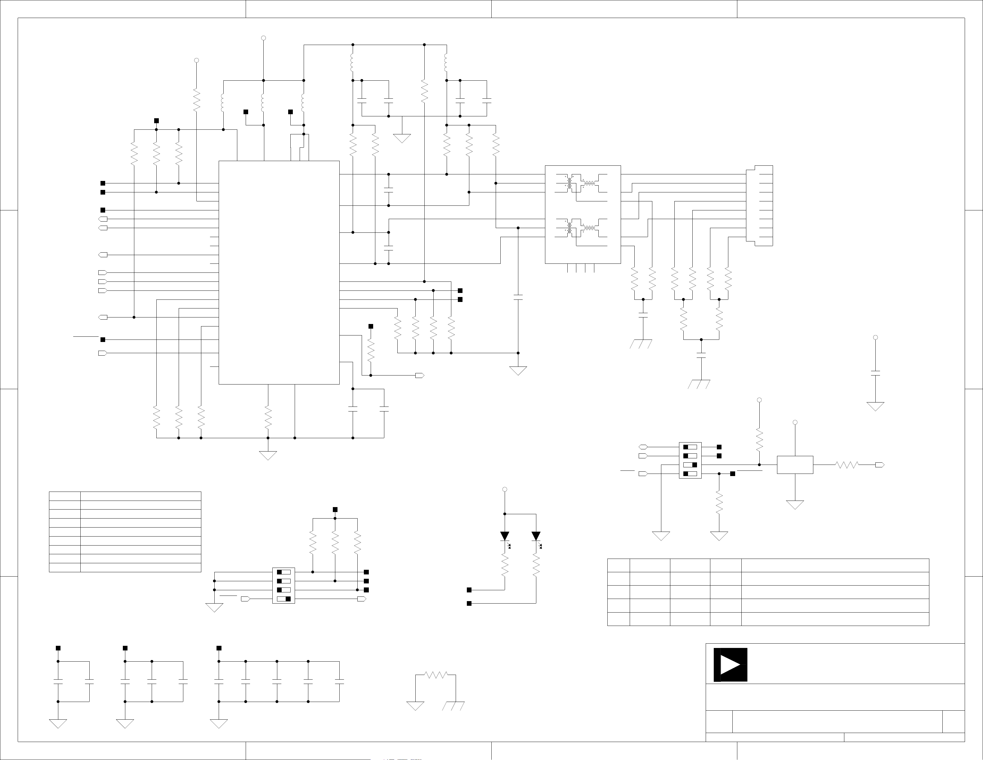
A B C
3.3V
D
3.3V
VDDIO
R86
10K
0402
DNP
FER16
600
0603
600
0603
FER15FER12
VDDA33VDD33
600
0603
1
R72
1.5K
0603
R157
10K
0402
U14
4
MDIO
2
MDC
15
RXD3/NINTSEL
16
RXD2/MODE2
17
RXD1/MODE1
18
RXD0/MODE0
19
RX_DV
20
RX_CLK/REGOFF
21
RX_ER/RXD4
22
TX_CLK
6
TX_EN
23
TXD0
24
TXD1
26
TXD2
27
TXD3
36
COL/RMII/CRS_DV
3
CRS/PHYAD4
5
NRST
14
CLKIN/XTAL1
13
XTAL2
LAN8700
QFN36
R76
10K
0402
25
VDDIO
7
VDD33
34
EXRES1
R67
12.4K
0603
"ETH MODE"
"FLASH CS"
SW9
1
1 2 3 4
2
3
4 5
DIP4
SWT018
30
35
33
VDD33A3
VDD33A1
VDD33A2
SPEED100/PHYAD0
LINK/PHYAD1
ACTIVITY/PHYAD2
FDUPLEX/PHYAD3
NINT/TX_ER/TX4
VDD_CORE
VSS/FLAG
37
R74
10K
0402
ON
8
7
6
TXP
TXN
RXP
RXN
VDDIO
MDIO
MDC
MODE2
ERXD1_HOSTD8
NDD6_ERXD0_HOSTD6
NDD1_ERXER_HOSTD1
NDD3_ETXEN_HOSTD3
NDD5_ETXD0_HOSTD5
NDD7_ETXD1_HOSTD7
R73
10K
0402
R71
1.5K
0603
2
NDD0_RMIICRSDV_HOSTD0
PHY_RESET
NDD4_RMIIREFCLK_HOSTD4
R158
10K
0402
3
SW9: Ethernet Mode Select (SW9.1, SW9.2, SW9.3)
MODE[2:0]
111
110
101
100
011
010
001
000
SW9.4 discconnects SPISEL1, for use on expansion interface (J2.11)
MODE DEFINITIONS
All Capable, Auto Negotiation
Power Down Mode
Repeater Mode, Auto Negotiation
100Base-TX Half duplex Advertised, Auto Negotiaion
100Base-TX Full Duplex
100Base-TX Half Duplex
10Base-T Full Duplex
10Base-T Half Duplex
DEFAULT
29
28
32
31
9
10
11
12
1
8
R55
10K
0402
FER14
600
0603
R91
10K
C118
3.3UF
0805
49.9
0603
TXP 1
TXN
RXP
RXN
VDDIO
R69
10K
0402
C131
4.7UF
0603
R75
10K
0402
MODE2
ERXD1_HOSTD8
NDD6_ERXD0_HOSTD6
SPI_FLASH_CSSPISEL1
R61R60
49.9
0603
C117
0.01UF
0402
C130
15PF
0402
C119
15PF
0402
C132
0.1UF
0402
R70
10K
0402
0402
R59
0402
TFS0A_RMIIMDINT#_HOSTCE#
FER13
600
0603
R62
49.9
R66
R65
10K
10K10K
0402
0402
DNP
LINKLED
ACTIVITYLED
C113
3.3UF
0805
R63
49.9
06030603
LINKLED
ACTIVITYLED
C116
0.01UF
0402
R64
10
0805
3.3V
LED6
YELLOW
LED001
R68
330.0
0402
U26
1
TD+
2
TCT
3
TD-
1CT:1CT
6
RD+
7
RCT
8
RD-
NC1
4
C112
0.22UF
0805
HX1188
ICS007
ICS007
PHY ADDRESS 0x01
LED7
GREEN
LED001
R77
330.0
0402
NC2
NC3
5
NC4
12
13
NDD2_MDIO_HOSTD2
MDC_HOSTRD#
16
TX+
14
TX-
15
TCM
11
RX+
9
RX-
10
TCM_
R85R84
R82
75.0
0603 0603
SHGND2
R81
75.0
C133
1000PF
1206
49.9
0603
R79
49.9
0603 0603
SHGND2
49.9
0603
R83
49.9
0603
C134
1000PF
1206
R78
49.9
"ETH ENABLE"
SW1
1 2 3 4
DIP4
SWT018
PHY (U14)
PHY (U14)
ON
8
7
6
MDIO
MDC
R169
10K
0402
OFF
OFF
ON
OFF
1
2
3
RESET
4 5
SW1: ETH Enable
POS. FROM TO DEFAULT
SW1.1
SW1.2
SW1.3
SW1.4
DSP (U2, PH2)
DSP (U2, PG14)
GND
RESET IC (U27)
RMII CLK (U24)
"ETHERNET"
J9
2
3
4
5
6
7
8
CON_RJ45_12P
R80
49.9
0603
3.3V
C155
0.01UF
0402
3.3V
3.3V
U24
"RMII CLK"
R166
10K
0402
4U24
VDD
1 3
OE OUT
PHY_RESET
ON (MDIO PHY U14), OFF (NAND U4, HOST connector P13.27, Expansion Interface J3.42)
ON (MDC PHY U14), OFF ( HOST connector P13.2, Expansion Interface J3.41)PHY (U14)
ON (RMII CLK disabled), OFF (RMII CLK enabled)
ON (PHY not held in reset), OFF (PHY held in reset)
50MHZ
OSC003
GND
2
FUNCTIONS
R167
33
0402
NDD4_RMIIREFCLK_HOSTD4
1
2
3
VDDIO
4
C128
10UF
0805 0402
C121
0.01UF
0402
C120
3.3UF
0805
C127 C126
0.01UF
0.01UF
0402
VDDA33VDD33
20 Cotton Road
Nashua, NH 03063
PH: 1-800-ANALOGD
4
C129
3.3UF
0805
0.01UF
0402 0402
C125 C124
0.01UF
0.01UF
0402 0402
C123C122
0.01UF
R58
0
0805
Title
ANALOG
DEVICES
ADSP-527 EZ-KIT Lite
RMII PHY
SHGND2
A B C D
Size Board No.
C
Date Sheet of
A0208-2006
7 1311-12-2007_13:59
Rev
1.4
Page 94
A B C
D
3.3V
LCD_DEN
R175
0
0402
SPISEL2#_CDG
SPISEL5#_HOSTD9
1
ERXD1_HOSTD8
3.3V
R174
0
0402
DNP
"KEY/PEN CS"
SW18
1 2
DIP2
SWT020
ON
4
3
1
2
R307
4.7K
0402
DT0PRIA_PPIFS3
KEY_PEN_CS
SW18: selects SPISEL2#(default) or SPISEL4#
Note: SPISEL4# conflicts with Ethernet (ERXD1), set SW1 to default
R93
10K
0402
R92
10K
0402
"KEYPAD"
"LCD"
"ENABLE"
FER18
600
0603
KEY_PEN_CS
SPISCK
SPIMOSI
1
2
28
27
26
U16
DVDD
AVDD
CS
SCLK
DIN
BUSY
DOUT
X+
Y+
25
24
3
5
X-
4
6
Y-
KEYPAD_BUSY
SPIMISO
X+
XY+
Y-
R306
0
0402
DNP
R94
10K
0402
DNP
LCD_PPIFS1
R305
10K
0402
3.3V
R95
10K
0402
DNP
R96
10K
0402
DNP
R97
10K
0402
DNP
UNREG_IN
C185
22UF
1210
C176
0.1UF
0603
5V
C175
10UF
0805
C174
0.1UF
0603
VR5
6
IN
7
RT
3
SD
4
GND
ADP1611
MSOP8
L3
8.2UH
IND014
SW1
FB
SS
COMP
TP10
D13
DFLS240
POWER_DI123
R300
R299
10.0K
0603
DNP
61.9K
0603
DNP
5
2
8
1
LCD_ADP1611_FB
C190
0.1UF
0603
R298
200.0K
0603
C245
220PF
0603
C246
0.1UF
0603
C244
10UF
1210
FER21
600
0805
C195
0.1UF
0603
LCD_BACKLIGHT
C251
0.1UF
0805
1
SW5
1 2 3 4
DIP4
SWT018
ON
8
7
6
LCD_RESET
C137
0.01UF
0402
1
2
3
4 5
UART1RTS_PENIRQ#
KEYIRQ#
HOSTWR#_LED1
RESET
2
3.3V
C138
0.01UF
0402
23
PENIRQ
22
KEYIRQ
12
REF
10
AUX1
11
AUX2
8
BAT1
9
BAT2
7
GND
MAX1233
QFN28
C4
C3
C2
C1
R4
R3
R2
R1
DACOUT
21
20
19
18
14
15
16
17
13
R188
0
0805
U16
SW5: Keypad LCD enable
POS. FROM TO DEFAULT
SW1.1
SW1.2
SW1.3
3
SW1.4
DSP (U2, PF10)
DSP (U2, PG11)
RESET IC (U27)
Keypad IC (U16) ON
Keypad IC (U16)DSP (U2, PF9)
LCD conn (P12)
LCD conn (P12)
ON
OFF
ON
OFF (SW10.3 used as GPIO RTS of UART1, expansion interface J2.31, J2.49, SPORT 1 conn P7.7, PPI conn P8.18
OFF (Expansion Interface pins: J2.33 J2.48, SPORT 1 conn P7.16, PPI conn P8.17)
ON (GPIO control of LCD_RESET), OFF (HOST conn P13.4, LED1, Expansion Interface J1.80, STAMP buffer U34.15)
OFF( LCD not connected to board reset)
"LCD"
5V
P12
1
LCD_DEN
LCD_PPIFS2
LCD_PPIFS1
LCD_PPICLK
LCD_PPID0
LCD_PPID1
LCD_PPID2
LCD_PPID3
LCD_PPID4
LCD_PPID5
3.3V
4
LCD_PPID6
LCD_PPID7
LCD_RESET
2
3
4
5
6
7
8
9
10
11
12
13
14
15
16
CON056
3.3V
FUNCTIONS
C255
10UF
0805
0.01UF
0402
LCD_ADP1611_FB
5V
C254C253
10UF
0805
C252
0.01UF
0402
P12P12
P2
1
2
3
4
5
6
7
8
9
IDC9X1
LCD_BACKLIGHT
X+
C196
0.01UF
0805
D6
MMSZ12T1G
SOD-123
R191
10K
0805
R190
10K
0805
"TOUCHSCREEN"
P18
1 2
3 4
CON059
DNP
C259
0.1UF
0402
DNP
C258
0.1UF
0402
DNP
"BACKLIGHT"
"POWER"
P19
1 2
3 4
CON058
DNP
R189
40.2
0805
C257
0.1UF
0402
DNP
C256
0.1UF
0402
DNP
TP11
YY+X-
"CPLD JTAG"
3.3V
C247
0.01UF
0402
LCD_PPICLK
LCD_PPIFS2
RESET
LCD_DEN
P17
1
2
3
4
5
6
IDC6X1
DNP
Title
3.3V
3.3V
R301
10K
0402
U33
26
VCCIIO
43
IO_GCK1
44
IO_GCK2
1
IO_GCK3
36
IO_GTS1
34
IO_GTS2
33
IO_GSR
40
IO0
41
IO1
42
IO2
2
IO3
3
IO4
5
IO5
6
IO6
7
IO7
8
IO8
12
R302
10K
0402
LCD_TCK
LCD_TDO
LCD_TDI
LCD_TMS
IO9
13
IO10
14
IO11
11
TCK
24
TDO
9
TDI
10
TMS
XC9536XL
VQ44
ANALOG
DEVICES
16
IO12
18
IO13
39
IO14
38
IO15
37
IO16
32
IO17
31
IO18
30
IO19
29
IO20
28
IO21
27
IO22
23
IO23
22
IO24
21
IO25
20
IO26
19
IO27
C249
0.1UF
0402
20 Cotton Road
Nashua, NH 03063
PH: 1-800-ANALOGD
ADSP-527 EZ-KIT Lite
LCD
3.3V
U33
LCD_PPIFS1
C250
0.01UF
0402
C248
0.01UF
0402
2
3
4
P17
Size Board No.
C
Date Sheet of
11-12-2007_13:59 13
A0208-2006
A B C D
Rev
1.4
8
Page 95
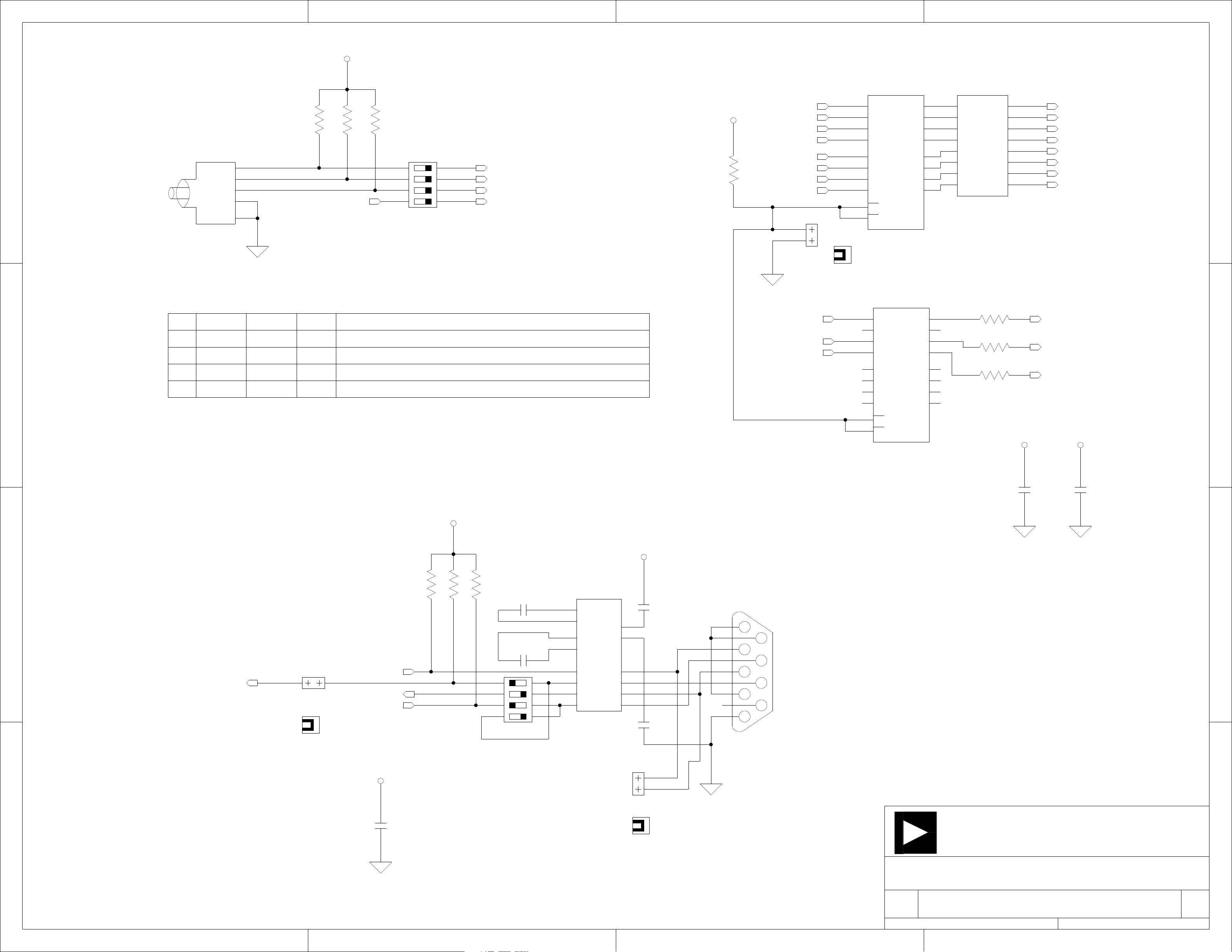
A B C
3.3V
D
"ROTARY"
"NAND"
R199
1.0K
0402
"ENCODER"
R197
1.0K
0402
1
SW3
1
A
3
B
4
SW1
5
SW2
ROTARY_ENCODER
COMMON
SWT022
2
NDCE#_HOSTD10
R200
1.0K
0402
"ENABLE"
SW11
1 2 3 4
DIP4
SWT018
ON
8
7
6
1
2
3
4 5
CUD
SPISEL2#_CDG
CZM
NDCE#
3.3V
R173
10K
0402
PPID0
PPID1
PPID2
PPID3
PPID4
PPID5
PPID6
PPID7
1
2
IDC2X1
JP2
SJ2
U31
2
1A1
4
1A2
6
1A3
8
1A4
11
2A1
13
2A2
15
2A3
17
2A4
1
OE1
19
OE2
IDT74FCT3244APY
SSOP20
SHORTING
JUMPER
DEFAULT=INSTALLED
1Y1
1Y2
1Y3
1Y4
2Y1
2Y2
2Y3
2Y4
18
16
14
12
9
7
5
3
RN5
16
R1B
15
R2B
14
R3B
13
R4B
12
R5B
11
R6B
10
R7B
9
R8B
0
RNS003
R1A
R2A
R3A
R4A
R5A
R6A
R7A
R8A
1
2
3
4
5
6
7
8
LCD_PPID0
LCD_PPID1
LCD_PPID2
LCD_PPID3
LCD_PPID4
LCD_PPID5
LCD_PPID6
LCD_PPID7
Populate JP2 when using LCD.
Connects PPI bus to LCD connector (P12)
1
"LCD PPI"
SW11: Rotary NAND enable
PPICLK
PPIFS1
PPIFS2
SW11.1
SW11.2
SW11.3
FROM DEFAULTPOS.
Encoder (SW3)
Encoder (SW3)
TO ALTERNATE FUNCTION / OFF MODE
DSP (U2, PF13)
DSP (U2, PF12)
DSP (U2, PF11)
ON
ON
ON
Expansion Interface (J2.34, J2.52) Stamp buffer (U34)
CS audio codec (U2), CS keypad/touch controller (U16), Expansion Interface (J2.30, J2.51), Stamp buffer (U30)
Expansion Interface (J2.32, J2.50), Stamp buffer (U34)Encoder (SW3)
2
SW11.4
DSP (U2, PH10)
NAND (U4)
ON
Host connector (P13.11), Expansion Interface (J3.35)
U32
2
1A1
4
1A2
6
1A3
8
1A4
11
2A1
13
2A2
15
2A3
17
2A4
1Y1
1Y2
1Y3
1Y4
2Y1
2Y2
2Y3
2Y4
18
16
14
12
9
7
5
3
R181
0
0402
R183
0
0402
R182
0
0402
LCD_PPICLK
LCD_PPIFS1
LCD_PPIFS2
2
1
OE1
19
OE2
IDT74FCT3244APY
SSOP20
C192
0.1UF
0402
3.3V
3.3V
10K
0402
R104R106
10K
0402
C158
0.1UF
0402
C157
0.1UF
0402
SW10
1 2 3 4
DIP4
SWT018
ON
1
2
3
4 5
U25
1
C1+
3
C1-
4
C2+
5
C2-
11
8
7
6
T1IN
10 7
T2IN T2OUT
ADM3202ARNZ
SOIC16
V+
T1OUT
R1INR1OUT
R2INR2OUT
2
6
V-
14
1312
89
C160
0.1UF
0402
C161
0.1UF
0402
J4
1
6
2
7
3
8
4
9
5
CON038
R105
10K
0402
3
Populate JP1 to control UART CTS
flow control by HWAIT_PUSHBUTTON1
"HWAIT ENABLE"
UART1TX
UART1RX
HWAIT_PUSHBUTTON1
JP1
1 2
IDC2X1
SJ3
UART1RTS_PENIRQ#
SHORTING
JUMPER
DEFAULT=NOT INSTALLLED
DNP
U31 U32
3.3V3.3V
C191
0.1UF
0402
3
"UART ENABLE"
3.3V
SERIAL PORT
(UART 1)
C156
0.01UF
0402
4
"UART LPBK"
U25
A B C D
JP5
1
2
IDC2X1
SJ1
SHORTING
JUMPER
DEFAULT=NOT INSTALLED
UART 1 Loop Jumper
ANALOG
20 Cotton Road
Nashua, NH 03063
PH: 1-800-ANALOGD
Title
DEVICES
ADSP-527 EZ-KIT Lite
ROTARY SWITCH, RS232
Size Board No.
C
Date Sheet of
A0208-2006
9 1311-12-2007_13:59
4
Rev
1.4
Page 96

A B C
3.3V
3.3V
3.3V
R178
10K
R121
10K
0402
"PB1"
1
SW15
MOMENTARY
SWT024
R124
100
0805
C164
1UF
0805
U17
74LVC14A
SOIC14
R127
10
0603
21
U22
C163
0.01UF
0402
LED0
HOSTWR#_LED1
HOSTACK_LED2
0402
R177
10K
0402
"GPIO ENABLE"
R120
10K
0402
"PB2"
SW14
MOMENTARY
SWT024
R122
100
0805
C165
1UF
0805
U17
13 12
74LVC14A
SOIC14
R128
10
0603
HOSTACK_LED2
KEYPAD_BUSY
USB_VRSEL
SW13
1 2 4 5 6
3
DIP6
SWT017
ON
1
2
3
4
5
6 7
12
11
10
9
8
HWAIT_PUSHBUTTON1
HOSTADDR_PUSHBUTTON2
PPI_SEL
HWAIT_PUSHBUTTON1
HOSTADDR_PUSHBUTTON2
R176
10K
0402
U22
2
1A1
4
1A2
6
1A3
8
1A4
11
2A1
13
2A2
15
2A3
17
2A4
1
OE1
19
OE2
IDT74FCT3244APY
SSOP20
1Y1
1Y2
1Y3
1Y4
2Y1
2Y2
2Y3
2Y4
18
16
14
12
9
7
5
3
LED3
YELLOW
LED001
R113
330
0603 0603
LED2
YELLOW
LED001
R112
330
D
LED1
YELLOW
LED001
R115
330
0603
3.3V
LED4
GREEN
LED001
R111
330
0603
1
"POWER"
2
2
SW13: GPIO enable
FROMPOS.
SW13.1
SW13.2
SW13.3
SW13.4
SW13.5
SW13.6
push button 1
push button 2
DSP(U2, PG12)
Keypad BUSY (U16) OFF (PB1, UART 1 CTS U25, Host conn P13.12, Expansion Interface J1.84), ON (GPIO Keypad busy U16, SW13.1)
OTG PWR(VR3, U28)
3
3.3V
R118
10K
0402
U17
9 8
74LVC14A
SOIC14
R125
10K
0402
74LVC14A
SOIC14
U17
TO DEFAULT
DSP (U2, PG0)
DSP (U2, PG13)
PPI CLK (U20)
DSP(U2, PG0)
DSP (U2, PG13)
R126
10K
0402
43
5 6
74LVC14A
SOIC14
U17
ON
ON
OFF
OFF
OFF
FUNCTIONS
ON (PB1), OFF (UART 1 CTS U25, HOST connector P13.12, Keypad busy SW13.8, Expansion Interface J1.84)
ON ( PB2), OFF (HOST connector P13.8, OTG voltage select SW13.7, Expansion Interface J1.85)
NCOFF
OFF (LED2, Host connector P13.10, Expansion Interface J1.81, STAMP buffer U34), ON (PPI CLK U20)
OFF (HOST connector P13.8, Expansion Interface J1.85), ON (PB2 SW13.11, OTG power VR3, U28)
R129
10K
0402
1
2
R119
10K
0402
74LVC14A
SOIC14
U17
"RESET"
DA_SOFT_RESET
1011
SW16
MOMENTARY
SWT024
U29
4
SN74LVC1G08
SOT23-5
R130
10K
0402
"RESET"
U27
4
RESETMR
PFI
RESET
ADM708SARZ
SOIC8
PFO
"HOST"
P13
IDC16X2
21
4
6
8
10
12
MDC_HOSTRD#
HOSTWR#_LED1
HOST_TFS0A_RMIIMDINT#_HOSTCE#
HOSTADDR_PUSHBUTTON2
HOSTACK_LED2
HWAIT_PUSHBUTTON1
RESET
3
32
NDALE_HOSTD15
NDCLE_HOSTD14
NDBUSY#_HOSTD13
NDRE#_HOSTD12
NDWR#_HOSTD11
NDCE#_HOSTD10
SPISEL5#_HOSTD9
ERXD1_HOSTD8
NDD7_ETXD1_HOSTD7
3.3V
LED5
RED
LED001
R131
10K
R123
330
0603
81
7
5
0402
RESET
NDD6_ERXD0_HOSTD6
NDD5_ETXD0_HOSTD5
NDD4_RMIIREFCLK_HOSTD4
NDD3_ETXEN_HOSTD3
NDD2_MDIO_HOSTD2
NDD1_ERXER_HOSTD1
NDD0_RMIICRSDV_HOSTD0
R193
22
0402
C197
15PF
0402
R194
22
0402
C198
15PF
0402
R195
22
0402
C199
15PF
0402
3
5
7
9
11
13 14
15 16
17 18
19 20
21 22
23 24
25 26
27 28
29 30
31
3.3V
C167
4
0.01UF
0402
3.3V 3.3V
C168
0.01UF
0402
C166
0.01UF
0402
Title
ANALOG
DEVICES
ADSP-527 EZ-KIT Lite
20 Cotton Road
Nashua, NH 03063
PH: 1-800-ANALOGD
4
LEDS, PUSHBUTTONS, RESET, HOST PORT
U17
U29
U27
A B C D
Size Board No.
C
Date Sheet of
A0208-2006
1011-13-2007_14:58 13
Rev
1.4
Page 97

1
2
3
HWAIT_PUSHBUTTON1
D[0:15]
A[1:19]
HOSTWR#_LED1
PPID0
PPID2
A B C
5V
J1
2
4
A1
A3
A5
A7
A9
A11
A13
A15
A17
A19
D1 D0
D3
D5
D7
D9
D11
D13
D15
R168
0
0603
6
8
10
20
30
40
50
60
70
80
90
1
3
5
7
9
1112
1314
1516
1718
19
2122
2324
2526
2728
29
3132
3334
3536
3738
39
4142
4344
4546
4748
49
5152
5354
5556
5758
59
6162
6364
6566
6768
69
7172
7374
7576
7778
79
8182
8384
8586
8788
89
CON019
A2
A4
A6
A8
A10
A12
A14
A16
A18
D2
D4
D6
D8
D10
D12
D14
PPICLK
PPID1
PPID3
LED0
HOSTACK_LED2
HOSTADDR_PUSHBUTTON2
"EXPANSION INTERFACE = TYPE B"
SPIMOSI SPISCK
SPIMISO
PPIFS2
UART1TX
SPISEL2#_CDG
CZM
CUD
SPIMOSI
DT0PRIA_PPIFS3
TFS0A_RMIIMDINT#_HOSTCE#
TSCLK0A
PPID5
PPID7
KEYIRQ#
CZM
CUD
UART1RX
UART1RX
SCL
ABE1#/SDQM1
ABE0#/SDQM0
AOE
AWE
SMS
SWE
J2
2
4
6
8
10
20
30
40
50
60
70
80
90
CON019
D
3.3V
3.3V
R198
10K
0402
R140
10K
5V3.3V 3.3V
1
3
5
7
9
1112
1314
1516
1718
19
2122
2324
2526
2728
29
3132
3334
3536
3738
39
4142
4344
4546
4748
49
5152
5354
5556
5758
59
6162
6364
6566
6768
69
7172
7374
7576
7778
79
8182
8384
8586
8788
89
SPISEL1
NMI
DT0PRIA_PPIFS3
PPIFS1
UART1RX
LED0
UART1RTS_PENIRQ#
KEYIRQ#
SPIMISO
DR0PRIA
RFS0A
RSCLK0A
PPID4
PPID6
LED0
UART1RTS_PENIRQ#
SPISEL2#_CDG
UART1TX
UART1TX
SDA
AMS3
AMS2
AMS1
AMS0
ARDY
ARE
ABE1#/SDQM1ABE0#/SDQM0
SCKESRAS
SCASSA10
CLKOUT
NDD7_ETXD1_HOSTD7
NDWR#_HOSTD11
NDD4_RMIIREFCLK_HOSTD4
NDBUSY#_HOSTD13
NDD0_RMIICRSDV_HOSTD0
NDD2_MDIO_HOSTD2 MDC_HOSTRD#
DR0PRIA
UART1TX
RESET
NDALE_HOSTD15
ERXD1_HOSTD8
NDRE#_HOSTD12
J3
2
4
6
8
10
20
30
40
50
60
70
80
90
CON019
1
3
5
7
9
1112
1314
1516
1718
19
2122
2324
2526
2728
29
3132
3334
3536
3738
39
4142
4344
4546
4748
49
5152
5354
5556
5758
59
6162
6364
6566
6768
69
7172
7374
7576
7778
79
8182
8384
8586
8788
89
RFS0A
UART1RX
NDD5_ETXD0_HOSTD5
SPISEL5#_HOSTD9
NDD3_ETXEN_HOSTD3
EXPANSION_PPI_CLK
CLKOUT
TFS0A_RMIIMDINT#_HOSTCE#
NDD6_ERXD0_HOSTD6
NDCE#_HOSTD10
NDCLE_HOSTD14
NDD1_ERXER_HOSTD1
0402
4
U19
VDD
1
OE
20MHZ
OSC003
GND
3.3V
2
OUT
R215
0
0402
3
"JTAG"
ZP4
1
3
5
7
9
11
13
IDC7X2
DA_SOFT_RESET
DSP JTAG HEADER
U19 U20
All USB interface circuitry is considered proprietary and has
been omitted from this schematic.
When designing your JTAG interface please refer to the
Engineer to Engineer Note EE-68 which can be found at
http://www.analog.com
RESET
EXPANSION_PPI_CLK
R139
33
0402
PPI_SEL
C187 C188
0.01UF
0402
2
4
6
8
10
12
14
DA_EMULATOR_SELECT
DA_EMULATOR_EMU
DA_EMULATOR_TMS
DA_EMULATOR_TCK
DA_EMULATOR_TRST
DA_EMULATOR_TDI
DA_EMULATOR_TDO
RESET
DA_SOFT_RESET
DEBUG_AGENT
GND
3
6
4
3.3V
3V
U20
ADG752BRTZ
SOT23-6
DA_GP0
DA_GP1
DA_GP2
DA_GP3
SHGND
TMS
TCK
TRST
TDI
TDO
EMU
1
3.3V
3.3V3.3V
R212
4.7K
0402
0.01UF
0402
R213
10K
0402
PPICLK
TMS
TCK
TRST
TDI
TDO
EMU
1
2
3
SHGND
ANALOG
20 Cotton Road
Nashua, NH 03063
4
Title
DEVICES
ADSP-527 EZ-KIT Lite
PH: 1-800-ANALOGD
4
EXPANSION INTERFACE & JTAG
Size Board No.
C
Date Sheet of
A B C D
11-9-2007_14:05 11 13
A0208-2006
Rev
1.4
Page 98

A B C
5V 3.3V
UNREG_IN
"SPORT 0"
P6
2 1
4
TSCLK0A
STAMP_DR0PRIA
1
STAMP_MISO
STAMP_MOSI
DT0PRIA_PPIFS3
STAMP_RSCLK0A
STAMP_MOSI
STAMP_MISO
STAMP_SPISCK
STAMP_SDA
STAMP_SCL
STAMP_DR0PRIA
STAMP_RFS0A
STAMP_RSCLK0A
6
8
10
12
32
IDC17X2
3
5
7
9
11
1314
1516
1718
1920
2122
2324
2526
2728
2930
31
3334
RESET
STAMP_RFS0A
STAMP_TFS0A_RMIIMDINT#_HOSTCE#
STAMP_SPISEL1#
STAMP_SPISEL2#_CDG
STAMP_CUD
STAMP_LED0
STAMP_HOSTWR#_LED1
STAMP_HOSTACK_LED2
STAMP_CUD
STAMP_LED0
UART1RX
UART1TX
STAMP_SPISEL2#_CDG
KEYIRQ#
STAMP_MOSI
STAMP_MISO
STAMP_SPISCK
STAMP_SDA
STAMP_SCL
STAMP_DR0PRIA
STAMP_RFS0A
STAMP_RSCLK0A
UNREG_IN
"SPORT 1"
P7
12
4
6
8
10
12
14 13
16 15
18 17
20 19
22 21
24 23
26 25
28 27
30 29
32
34 33
3
5
7
9
11
31
IDC17X2
3.3V5V
SCL
SDA
SPISCK
SPISEL1
SPIMOSI
JP3
1
2
IDC2X1
"STAMP ENABLE"
STAMP_RSCLK0A
STAMP_DR0PRIA
STAMP_RFS0A
CUD
LED0
HOSTWR#_LED1
HOSTACK_LED2
RESET
UART1RTS_PENIRQ#
STAMP_CZM
STAMP_SPISEL1#
STAMP_SPISEL2#_CDG
STAMP_CUD
STAMP_LED0
STAMP_HOSTWR#_LED1
STAMP_HOSTACK_LED2
3.3V
R184
10K
0402
SPISEL2#_CDG
U30
2
1A1
4
1A2
6
1A3
8
1A4
11
2A1
13
2A2
15
2A3
17
2A4
1
OE1
19
OE2
CBT3244A
SSOP20
U34
2
1A1
4
1A2
6
1A3
8
1A4
11
2A1
13
2A2
15
2A3
17
2A4
18
1Y1
16
1Y2
14
1Y3
12
1Y4
9
2Y1
7
2Y2
5
2Y3
3
2Y4
Populating JP3 enables signals from U33
and U34 to connectors on this page.
18
1Y1
16
1Y2
14
1Y3
12
1Y4
9
2Y1
7
2Y2
5
2Y3
3
2Y4
D
STAMP_SCL
STAMP_SDA
STAMP_SPISCK
STAMP_SPISEL1#
STAMP_SPISEL2#_CDG
SPIMISOSTAMP_MISO
STAMP_MOSI
SJ4
SHORTING
JUMPER
DEFAULT=NOT INSTALLLED
DNP
RSCLK0A
DR0PRIA
RFS0A
STAMP_CZMCZM
STAMP_CUD
STAMP_LED0
STAMP_HOSTWR#_LED1
STAMP_HOSTACK_LED2
1
UNREG_IN
2
PPICLK
PPID0
PPID2
PPID4
PPID6
STAMP_LED0
UART1RTS_PENIRQ#
STAMP_SPISEL2#_CDG
UART1TX
STAMP_LED0
STAMP_SPISEL2#_CDG
RESET
STAMP_MOSI
STAMP_MISO
STAMP_SPISCK
3
STAMP_SDA
STAMP_SCL
"PPI"
P8
2
4
10
20
30
40
IDC20X2
5V 3.3V
1
3
56
78
9
1112
1314
1516
1718
19
2122
2324
2526
2728
29
3132
3334
3536
3738
39
PPID1
PPID3
PPID5
PPID7
KEYIRQ#
STAMP_CZM
STAMP_CUD
UART1RX
STAMP_CUD
STAMP_SPISEL1#
DT0PRIA_PPIFS3
PPIFS1
PPIFS2
STAMP_SDA
STAMP_LED0
STAMP_HOSTACK_LED2
3.3V 5V
"TWI"
P10
2
4
6
8
10
12
14
16
18
20
1
3
5
7
9
11
13
15
17
19
IDC10X2
UNREG_IN
STAMP_SCL
RESET
STAMP_HOSTWR#_LED1
UNREG_IN
"SPI"
P9
2
4
6
STAMP_SPISCK
STAMP_SPISEL1# STAMP_SPISEL2#_CDG
STAMP_CUD
STAMP_LED0
STAMP_HOSTACK_LED2
8
10
12
14
16
18
20
IDC10X2
5V3.3V
1
3
5
7
9
11
13
15
17
19
STAMP_MOSISTAMP_MISO
RESET
STAMP_HOSTWR#_LED1
1
OE1
19
OE2
CBT3244A
SSOP20
"TFS0A/HOSTCE"
3.3V
C194
0.1UF
0402
3.3V
U30U34
C193
0.1UF
0402
2
3
"ENABLE"
SW21
1 2
DIP2
SWT020
ON
4
3
TFS0A_RMIIMDINT#_HOSTCE#
TFS0A_RMIIMDINT#_HOSTCE#
3.3V 5V
3.3V5V
"UART 0"
HOST_TFS0A_RMIIMDINT#_HOSTCE#
STAMP_TFS0A_RMIIMDINT#_HOSTCE#
SW21 disconnects TFS0A_RMIIMDINT#_HOSTCE#
from SPORT conn P6.11 and HOST conn P13.6
1
2
"TIMERS"
P5
P11
2
STAMP_DR0PRIA
4
STAMP_RSCLK0A
6
10
IDC5X2
1
34
5
78
9
STAMP_LED0
STAMP_HOSTWR#_LED1
STAMP_HOSTACK_LED2
STAMP_DR0PRIA
STAMP_RFS0ASTAMP_RFS0A
2
4 3
6
8 7
10
IDC5X2
1
5
9
STAMP_HOSTWR#_LED1
STAMP_HOSTACK_LED2
Title
ANALOG
DEVICES
ADSP-527 EZ-KIT Lite
20 Cotton Road
Nashua, NH 03063
PH: 1-800-ANALOGD
4
STAMP CONNECTORS
Size Board No.
C
Date Sheet of
11-6-2007_15:28 12 13
A0208-2006
Rev
1.4
A B C D
Page 99

A B C
D
5V_USB
R170
0
0805
DNP
R146
210.0K
0805
R145
64.9K
0805
USB_VRSEL
C177
4.7UF
0805
R116
0
0402
R117
1K
0603
DNP
U28
7 6
IN1 OUT1
1
EN
C148
1UF
0805
GND
3
OUT2
FLG
MIC2025-1
SOIC8
"5V USB"
5V_USB
8
2
Unpopulate P14 when measuring VDDINT
C159
1UF
0805
1
7
8
VR3
IN1
IN2
D8
ZHCS1000
SOT23-312
DNP
GND
4
ADP3336ARMZ
MSOP8
OUT1
OUT2
OUT3
FBSD
1
2
3
56
D12
MBRS540T3G
5A
SMC
C147
10UF
1210
UNREG_IN
R107
10K
0402
10K
0402
DNP
3.3V
C144
1UF
0805
7
8
VR4
IN1
IN2
OUT1
OUT2
OUT3
GND
4
ADP3336ARMZ
MSOP8
UNREG_IN
D7
ZHCS1000
SOT23-312
R135
10K
"2.5V"
1
2
3
56
FBSD
R137
105.0K
0603R108
R136
95K
0603
2.5V
C143
4.7UF
0805
USB_VRSEL
R110
0
0402
0402
DNP
R144
10K
0402
C178
1UF
0805
J6
1
7_0V_POWER
CON005
F2
5A
FUS005
C180
2
3
1000PF
1206
D11
MBRS540T3G
5A
SMC
FER17
190
FER002
4
1
3
2
1
FER19
600
1206
FER20
600
1206
SHGND
C179
1000PF
1206
SHGND
SJ9
SHORTING
UNREG_IN
C184
10UF
1210
C181
10UF
0805
DNP
2
PGND
C182
470PF
0603
R150
24.9K
0603
C183
68PF
0603
R151
80.6K
0603
R152
255.0K
0603
VR1
1
COMP
GND
2
5
IN
4
CS
63
PGATEFB
ADP1864AUJZ
SOT23-6
R133
0
0603
R134
0.05
1206
R132
0.05
1206
U18
DNP
1
2
3
4
SI4411DY
SO-8 D2E
5
6
7
8
L2
2.5UH
IND013
D10
MBRS540T3G
SMC
CT11
220UF
Unpopulate P15 when measuring VDDEXT
SJ8
SHORTING
3.3V @ 2A
TP6
CT12
2.2UF
B
DNP
C171
4.7UF
0805
3.3V
"VDDEXT"
P15
1 2
IDC2X1
R142
0.05
1206
R141
0.05
1206
JUMPER
DEFAULT=INSTALLLED
VDDEXT
VDDMEM
TP15
TP16
VROUT
R149
0
0402
CT9
100UF
C
C170
10UF
0805
3.3V
C169
0.1UF
0603
U21
1
2
3
4
FDS9431A
SOIC8
"VDDINT"
P14
1 2
IDC2X1
L1
10UH
5
6
7
8
IND001
D9
ZHCS1000
SOT23-312
R143
0.05
1206
CT10
100UF
C
JUMPER
DEFAULT=INSTALLLED
TP5
VDDINT
TP17
2
PGND
PGND
W3
COPPER
3
UNREG_IN
CT6
100UF
C
PGND
PGND2
PGND2
C139
22UF
1210
GND
2
5
IN
4
CS
63
PGATEFB
ADP1864AUJZ
SOT23-6
R102
0
0603
R103
0.027
1206
R101
0.027
1206
U23
1
2
3
4
SI4411DY
SO-8
5
6
7
8
PGND2
L4
2.5UH
IND013
D5
MBRS540T3G
SMC
C142
22UF
1210
R100
422K
0603
VR2
1
COMP
C140
470PF
0603
R98
24.9K
0603
C141
68PF
0603
R99
80.6K
0603
4
4A
"5V"
TP14
C145
22UF
1210
5V
5V @ 1A
CT14
47UF
D
DNP
W4
COPPER
4A
P16
1 2
IDC2X1
"VDDMEM"
SJ7
SHORTING
JUMPER
DEFAULT=INSTALLLED
Unpopulate P16 when measuring VDDMEM
M1
RUBBER FOOT
MSC009
DNP
RUBBER FOOT
MSC009
M4
RUBBER FOOT
MSC009
DNP
TP12 TP4 TP9TP8 TP7
M2
DNP
RUBBER FOOT
MSC009
"GND"
M3
RUBBER FOOT
MSC009
DNP
M5
DNP
Title
MH5
MH9
ANALOG
DEVICES
ADSP-527 EZ-KIT Lite
MH4MH3MH2MH1
MH11
MH12MH10MH8 MH13
20 Cotton Road
Nashua, NH 03063
PH: 1-800-ANALOGD
3
MH14MH7MH6
MH15
4
POWER
PGND2
A B C D
Size Board No.
C
A0208-2006
Date Sheet of
Rev
1.4
1311-12-2007_13:59 13
Page 100

A ADSP-BF527 EZ-KIT LITE BILL
OF MATERIALS
The bill of materials corresponds to “ADSP-BF527 EZ-KIT Lite Sche-
matic” on page B-1.
Ref. Qty. Description Reference
Designator
1 1 74LVC14A
SOIC14
2 3 IDT74FCT3244
APY SSOP20
3 1 SN74AHC1G00
SOT23-5
4 1 32.768KHZ
OSC008
5 1 25MHZ OSC003 U3 EPSON SG-8002CA MP
6 4 SN74LVC1G08
SOT23-5
7 1 FDS9431A
SOIC8
8 1 MT48LC32M16
A2TG-75
TSOP54
9 1 20MHz OSC003 U19 DIGI-KEY SG-8002CA-PCC-ND
10 2 SI4411DY SO-8 U18,U23 VISHAY Si4411DY-T1-E3
U17 TI 74LVC14AD
U22,U31-32 IDT IDT74FCT3244APYG
U6 TI SN74AHC1G00DBVR
U1 EPSON MC-156-32.7680KA-A0:
U9-11,U29 TI SN74LVC1G08DBVR
U21 FAIRCHILD FDS9431A
U7 MICRON MT48LC32M16A2P-75
Manufacturer Part Number
ROHS
(20.000M)
11 1 HX1188 ICS007 U26 DIGI-KEY 553-1340-ND
12 1 24MHZ OSC003 U12 EPSON SG-8002CA-MP
ADSP-BF527 EZ-KIT Lite Evaluation System Manual A-1
 Loading...