


ADSP-BF518F EZ-Board
TM
Evaluation System Manual
Analog Devices, Inc.
One Technology Way
Norwood, Mass. 02062-9106
Revision 1.1, June 2009
Part Number
82-000217-01

Copyright Information
© 2009 Analog Devices, Inc., ALL RIGHTS RESERVED. This document may not be reproduced in any form without prior, express written
consent from Analog Devices, Inc.
Printed in the USA.
Disclaimer
Analog Devices, Inc. reserves the right to change this product without
prior notice. Information furnished by Analog Devices is believed to be
accurate and reliable. However, no responsibility is assumed by Analog
Devices for its use; nor for any infringement of patents or other rights of
third parties which may result from its use. No license is granted by implication or otherwise under the patent rights of Analog Devices, Inc.
Trademark and Service Mark Notice
The Analog Devices logo, VisualDSP++, Blackfin, EZ-KIT Lite, and
EZ-Extender are registered trademarks of Analog Devices, Inc. EZ-Board
is a trademark of Analog Devices, Inc.
All other brand and product names are trademarks or service marks of
their respective owners.

Regulatory Compliance
The ADSP-BF518F EZ-Board is designed to be used solely in a laboratory
environment. The board is not intended for use as a consumer end product or as a portion of a consumer end product. The board is an open
system design which does not include a shielded enclosure and therefore
may cause interference to other electrical devices in close proximity. This
board should not be used in or near any medical equipment or RF devices.
The ADSP-BF518F EZ-Board has been certified to comply with the
essential requirements of the European EMC directive 2004/108/EC and
therefore carries the “CE” mark.
The ADSP-BF518F EZ-Board has been appended to Analog Devices, Inc.
EMC Technical File (EMC TF) referenced DSPTOOLS1, issue 2 dated
June 4, 2008 and was declared CE compliant by an appointed Notified
Body (No.0673) as listed below.
Notified Body Statement of Compliance: Z600ANA2.032, dated March,
2009.
Issued by: Technology International (Europe) Limited
60 Shrivenham Hundred Business Park
Shrivenham, Swindon, SN6 8TY, UK
The EZ-Board evaluation system contains ESD (electrostatic discharge)
sensitive devices. Electrostatic charges readily accumulate on the human
body and equipment and can discharge without detection. Permanent
damage may occur on devices subjected to high-energy discharges. Proper
ESD precautions are recommended to avoid performance degradation or
loss of functionality. Store unused EZ-Board boards in the protective shipping package.


CONTENTS
PREFACE
Product Overview ......................................................................... xiii
Purpose of This Manual .................................................................. xv
Intended Audience ......................................................................... xvi
Manual Contents ........................................................................... xvi
What’s New in This Manual .......................................................... xvii
Technical or Customer Support ..................................................... xvii
Supported Processors .................................................................... xviii
Product Information .................................................................... xviii
Analog Devices Web Site ........................................................ xviii
VisualDSP++ Online Documentation ....................................... xix
Technical Library CD ............................................................... xix
Related Documents ................................................................... xx
Notation Conventions .................................................................... xxi
USING ADSP-BF518F EZ-BOARD
Package Contents .......................................................................... 1-3
Default Configuration ................................................................... 1-4
EZ-Board Installation ................................................................... 1-4
ADSP-BF518F EZ-Board Evaluation System Manual v

CONTENTS
EZ-Board Session Startup ............................................................. 1-6
Evaluation License Restrictions ..................................................... 1-8
Memory Map ............................................................................... 1-9
SDRAM Interface ....................................................................... 1-10
Parallel Flash Memory Interface .................................................. 1-11
eMMC Interface ......................................................................... 1-12
SD Interface ............................................................................... 1-12
SPI Interface .............................................................................. 1-13
Parallel Peripheral Interface (PPI) ................................................ 1-14
Rotary Encoder Interface ............................................................ 1-15
Ethernet Interface ....................................................................... 1-15
Audio Interface ........................................................................... 1-16
ADC Interface ............................................................................ 1-17
UART Interface .......................................................................... 1-18
RTC Interface ............................................................................ 1-19
LEDs and Push Buttons .............................................................. 1-20
JTAG Interface ........................................................................... 1-21
Land Grid Array ......................................................................... 1-21
Expansion Interface II ................................................................. 1-22
Power Measurements .................................................................. 1-23
Power-On-Self Test ..................................................................... 1-23
Example Programs ...................................................................... 1-24
Background Telemetry Channel .................................................. 1-24
Reference Design Information ..................................................... 1-24
vi ADSP-BF518F EZ-Board Evaluation System Manual

CONTENTS
ADSP-BF518F EZ-BOARD HARDWARE REFERENCE
System Architecture ...................................................................... 2-2
Programmable Flags ...................................................................... 2-3
Push Button and Switch Settings ................................................... 2-7
Boot Mode Select Switch (SW1) .............................................. 2-8
PB Enable Switch (SW2) ......................................................... 2-8
Flash Enable Switch (SW3) ...................................................... 2-9
SPORT1 Enable Switch (SW4) ................................................ 2-9
MIC Gain/Loopback Switch (SW5) ....................................... 2-10
UART Setup Switch (SW10) ................................................. 2-10
Reset Push Button (SW11) .................................................... 2-11
Programmable Flag Push Buttons (SW12–13) ........................ 2-11
Rotary Encoder with Momentary Switch (SW14) .................. 2-12
SPORT0 ENBL Switch (SW15) ............................................. 2-12
Encoder Enable Switch (SW19) ............................................. 2-12
eMMC Enable Switch (SW20–21) ......................................... 2-13
ADC Loopback Switches (SW22–23) ..................................... 2-13
Jumpers ...................................................................................... 2-14
Flash WP Jumper (JP3) ......................................................... 2-15
OTP Flag Enable Jumper (JP14) ............................................ 2-15
MIC Select Jumper (JP15) ..................................................... 2-16
SPI FLASH CS Enable Jumper (JP16) ................................... 2-16
Ethernet Power Down Jumper (JP17) ..................................... 2-16
Ethernet Isolate Jumper (JP18) .............................................. 2-16
ADSP-BF518F EZ-Board Evaluation System Manual vii

CONTENTS
VDDINT Power Jumper (P8) ............................................... 2-16
VDDEXT Power Jumper (P9) ............................................... 2-17
VDDMEM Power Jumper (P10) ........................................... 2-17
VDDFLASH Power Jumper (P11) ......................................... 2-17
LEDs ......................................................................................... 2-18
GPIO LEDs (LED1–3) ......................................................... 2-19
Reset LED (LED9) ............................................................... 2-19
Power LED (LED13) ............................................................ 2-19
Speed LED (LED14) ............................................................. 2-19
Connectors ................................................................................. 2-20
Expansion Interface II Connector (J1) ................................... 2-21
RS-232 Connector (J2) ......................................................... 2-21
Power Connector (J3) ........................................................... 2-21
Dual Audio Connectors (J4–5) .............................................. 2-22
Battery Holder (J12) ............................................................. 2-22
SD Connector (J13) .............................................................. 2-22
Ethernet Connectors (J14–15) .............................................. 2-22
JTAG Connector (P1) ........................................................... 2-23
Expansion Interface II Connectors (P2 and P4) ..................... 2-23
Expansion Interface II Connector (P3) .................................. 2-23
DMAX Land Grid Array Connectors (P5–7) ......................... 2-24
Standalone Debug Agent Connector (ZP1) ............................ 2-24
viii ADSP-BF518F EZ-Board Evaluation System Manual

CONTENTS
ADSP-BF518F EZ-BOARD BILL OF MATERIALS
ADSP-BF518F EZ-BOARD SCHEMATIC
Title Page .................................................................................... B-1
Processor EBIU and Control ........................................................ B-2
Processor Power, Bypass Caps ....................................................... B-3
External Memory ......................................................................... B-4
ADC Inputs ................................................................................. B-5
ADC ........................................................................................... B-6
Audio Codec ................................................................................ B-7
Ethernet PHY .............................................................................. B-8
Rotary Encoder, JTAG, RS-232, EMMC, CD .............................. B-9
Logic Analyzer Conn .................................................................. B-10
Reset, LEDs, Push Buttons ......................................................... B-11
Expansion Interface .................................................................... B-12
OTP and Dual Power ................................................................. B-13
Power ........................................................................................ B-14
Series Terminators ...................................................................... B-15
INDEX
ADSP-BF518F EZ-Board Evaluation System Manual ix

CONTENTS
x ADSP-BF518F EZ-Board Evaluation System Manual

PREFACE
Thank you for purchasing the ADSP-BF518F EZ-Board™, Analog
Devices, Inc. evaluation system for ADSP-BF512/BF512F,
ADSP-BF514/BF514F, ADSP-BF516/BF516F, and
ADSP-BF518/BF518F Blackfin® processors.
Blackfin processors embody a new type of embedded processor designed
specifically to meet the computational demands and power constraints of
today’s embedded audio, video, and communications applications. They
deliver breakthrough signal-processing performance and power efficiency
within a reduced instruction set computing (RISC) programming model.
Blackfin processors support a media instruction set computing (MISC)
architecture. This architecture is the natural merging of RISC, media
functions, and digital signal processing (DSP) characteristics. Blackfin
processors deliver signal-processing performance in a microprocessor-like
environment.
Based on the Micro Signal Architecture (MSA), Blackfin processors combine a 32-bit RISC instruction set, dual 16-bit multiply accumulate
(MAC) DSP functionality, and eight-bit video processing performance
that had previously been the exclusive domain of very-long instruction
word (VLIW) media processors.
The evaluation board is designed to be used in conjunction with the VisualDSP++® development environment to test the capabilities of the
ADSP-BF512/BF512F, ADSP-BF514/BF514F, ADSP-BF516/BF516F,
ADSP-BF518F EZ-Board Evaluation System Manual xi

and ADSP-BF518/BF518F Blackfin processors. The VisualDSP++ development environment aids advanced application code development and
debug, such as:
• Create, compile, assemble, and link application programs written
in C++, C, and assembly
• Load, run, step, halt, and set breakpoints in application programs
• Read and write data and program memory
• Read and write core and peripheral registers
• Plot memory
Access to the processor from a personal computer (PC) is achieved
through a USB port or an external JTAG emulator. The USB interface of
the standalone debug agent gives unrestricted access to the processor and
evaluation board’s peripherals. Analog Devices JTAG emulators offer
faster communication between the host PC and target hardware. To learn
more about Analog Devices emulators and processor development tools,
go to
http://www.analog.com/dsp/tools/.
The ADSP-BF518F EZ-Board provides example programs to demonstrate
the capabilities of the product.
L
xii ADSP-BF518F EZ-Board Evaluation System Manual
The ADSP-BF518F EZ-Board installation is part of the VisualDSP++ installation. As an EZ-KIT Lite, an EZ-Board is a
licensed product that offers an unrestricted evaluation license for
the first 90 days. For details about evaluation license restrictions
after the 90 days, refer to “Evaluation License Restrictions” on
page 1-8 and the VisualDSP++ Installation Quick Reference Card.

Product Overview
The board features:
• Analog Devices ADSP-BF518F Blackfin processor
D Core performance up to 400 MHz
D External bus performance up to 80 MHz
D 176-pin LQFP package
D 25 MHz crystal
• Programmable VDDINT core power
D Analog Devices AD5258 TWI digital potentiometer
D Analog Devices ADP1715 low dropout linear regulator
• Synchronous dynamic random access memory (SDRAM)
Preface
D Micron MT48LC32M16A2TG – 64 MB (32M x 16-bits)
• Parallel flash memory
D Numonyx M29W320EB – 4 MB (2M x 16-bits)
• eMMC flash memory
D Micron MTFC2GDKDM – 2 GB
• SPI flash memory
D Numonyx M25P16 – 16 Mb
ADSP-BF518F EZ-Board Evaluation System Manual xiii

Product Overview
• Analog audio interface
D Analog Devices SSM2603 low-power audio codec
D One stereo LINE OUT jack
D One headphone LINE IN
D
One input MIC jack
D One input stereo LINE IN jack
• Ethernet interface
D National Semiconductor DP83848 PHY device
D 10-BaseT and 100-BaseTX
D Auto-MDIX
• ADC interface
D Analog Devices AD7266 2 MSPS, 12-bit, 3-channel SAR
analog-to-digital converter
• Thumbwheel
D Panasonic EVQ-WKA001 rotary encoder
• Universal asynchronous receiver/transmitter (UART)
D ADM3202 RS-232 line driver/receiver
D DB9 female connector
•LEDs
D Five LEDs: one board reset (red), three general-purpose
(amber), one configurable ethernet LEDs (amber) and one
power (green)
xiv ADSP-BF518F EZ-Board Evaluation System Manual

• Push buttons
D Three push buttons: one reset, two programmable flags with
debounce logic
• Expansion interface II
D Next generation of the expansion interface design, provides
access to most of the ADSP-BF518F processor signals
• Land grid array
D Easy probing of all port pins and most EBIU signals
• Other features
D JTAG ICE 14-pin header
D Blackfin power measurement jumpers
Preface
For information about the hardware components of the EZ-Board, refer
to “ADSP-BF518F EZ-Board Hardware Reference” on page 2-1.
Purpose of This Manual
The ADSP-BF518F EZ-Board Evaluation System Manual provides instructions for installing the product hardware (board). The text describes
operation and configuration of the board components and provides guidelines for running your own code on the ADSP-BF518F EZ-Board.
Finally, a schematic and a bill of materials are provided for reference.
The product software installation is detailed in the VisualDSP++ Installa-
tion Quick Reference Card.
ADSP-BF518F EZ-Board Evaluation System Manual xv

Intended Audience
Intended Audience
The primary audience for this manual is a programmer who is familiar
with Analog Devices processors. This manual assumes that the audience
has a working knowledge of the appropriate processor architecture and
instruction set. Programmers who are unfamiliar with Analog Devices
processors can use this manual, but should supplement it with other texts
(such as the ADSP-BF51x Blackfin Processor Hardware Reference and
Blackfin Processor Instruction Set Reference) that describe your target
architecture.
Programmers who are unfamiliar with VisualDSP++ should refer to the
VisualDSP++ online Help and user’s or getting started guides. For the
locations of these documents, see “Related Documents”.
Manual Contents
The manual consists of:
• Chapter 1, “Using ADSP-BF518F EZ-Board” on page 1-1
Describes EZ-Board functionality from a programmer’s perspective
and provides an easy-to-access memory map.
• Chapter 2, “ADSP-BF518F EZ-Board Hardware Reference” on
page 2-1
Provides information on the EZ-Board hardware components.
• Appendix A, “ADSP-BF518F EZ-Board Bill Of Materials” on
page A-1
Provides a list of components used to manufacture the EZ-Board.
• Appendix B, “ADSP-BF518F EZ-Board Schematic” on page B-1
Provides the resources to allow board-level debugging or to use as a
reference guide. Appendix B is part of the online Help.
xvi ADSP-BF518F EZ-Board Evaluation System Manual

Preface
What’s New in This Manual
The ADSP-BF518F EZ-Board Evaluation System Manual has been updated
to reflect the latest board revision. In addition, modifications and corrections based on errata reports against the previous manual revision have
been made.
Technical or Customer Support
You can reach Analog Devices, Inc. Customer Support in the following
ways:
• Visit the Embedded Processing and DSP products Web site at
http://www.analog.com/processors/technical_support
• E-mail tools questions to
processor.tools.support@analog.com
• E-mail processor questions to
processor.support@analog.com (World wide support)
processor.europe@analog.com (Europe support)
processor.china@analog.com (China support)
• Phone questions to 1-800-ANALOGD
• Contact your Analog Devices, Inc. local sales office or authorized
distributor
• Send questions by mail to:
Analog Devices, Inc.
One Technology Way
P.O. Box 9106
Norwood, MA 02062-9106
USA
ADSP-BF518F EZ-Board Evaluation System Manual xvii

Supported Processors
Supported Processors
This evaluation system supports Analog Devices ADSP-BF512/BF512F,
ADSP-BF514/BF514F, ADSP-BF516/BF516F, and
ADSP-BF518/BF518F Blackfin embedded processors.
Product Information
Product information can be obtained from the Analog Devices Web site,
VisualDSP++ online Help system, and a technical library CD.
Analog Devices Web Site
The Analog Devices Web site, www.analog.com, provides information
about a broad range of products—analog integrated circuits, amplifiers,
converters, and digital signal processors.
To access a complete technical library for each processor family, go to
http://www.analog.com/processors/technical_library. The manuals
selection opens a list of current manuals related to the product as well as a
link to the previous revisions of the manuals. When locating your manual
title, note a possible errata check mark next to the title that leads to the
current correction report against the manual.
Also note, MyAnalog.com is a free feature of the Analog Devices Web site
that allows customization of a Web page to display only the latest information about products you are interested in. You can choose to receive
weekly e-mail notifications containing updates to the Web pages that meet
your interests, including documentation errata against all manuals.
MyAnalog.com provides access to books, application notes, data sheets,
code examples, and more.
Visit
MyAnalog.com to sign up. If you are a registered user, just log on.
Your user name is your e-mail address.
xviii ADSP-BF518F EZ-Board Evaluation System Manual

Preface
VisualDSP++ Online Documentation
Online documentation comprises the VisualDSP++ Help system, software
tools manuals, hardware tools manuals, processor manuals, Dinkum
Abridged C++ library, and FLEXnet License Tools software documentation. You can search easily across the entire VisualDSP++ documentation
set for any topic of interest.
For easy printing, supplementary Portable Documentation Format (.pdf)
files for all manuals are provided on the VisualDSP++ installation CD.
Each documentation file type is described as follows.
File Description
.chm Help system files and manuals in Microsoft help format
.htm or
.html
.pdf VisualDSP++ and processor manuals in PDF format. Viewing and printing the
Dinkum Abridged C++ library and FLEXnet License Tools software documentation. Viewing and printing the .html files requires a browser, such as Internet
Explorer 6.0 (or higher).
.pdf files requires a PDF reader, such as Adobe Acrobat Reader (4.0 or higher).
Technical Library CD
The technical library CD contains seminar materials, product highlights, a
selection guide, and documentation files of processor manuals, VisualDSP++ software manuals, and hardware tools manuals for the following
processor families: Blackfin, SHARC, TigerSHARC, ADSP-218x, and
ADSP-219x.
To order the technical library CD, go to http://www.analog.com/proces-
sors/technical_library
processor, click the request CD check mark, and fill out the order form.
, navigate to the manuals page for your
ADSP-BF518F EZ-Board Evaluation System Manual xix

Product Information
Data sheets, which can be downloaded from the Analog Devices Web site,
change rapidly, and therefore are not included on the technical library
CD. Technical manuals change periodically. Check the Web site for the
latest manual revisions and associated documentation errata.
Related Documents
For information on product related development software, see the following publications.
Table 1. Related Processor Publications
Title Description
ADSP-BF512/ADSP-BF514/ADSP-BF516/ADSPBF518 Blackfin Embedded Processor Preliminary
Data Sheet
ADSP-BF51x Blackfin Processor Hardware Reference
Blackfin Processor Programming Reference Description of all allowed processor assem-
General functional description, pinout, and
timing of the processor.
Description of internal processor architecture and all register functions.
bly instructions.
Table 2. Related VisualDSP++ Publications
Title Description
ADSP-BF518F EZ-Board Evaluation System Manual
VisualDSP++ User’s Guide Description of VisualDSP++ features and
VisualDSP++ Assembler and Preprocessor Manuals Description of the assembler function and
VisualDSP++ C/C++ Complier and Library Manual for Blackfin Processors
Description of the hardware capabilities of
the evaluation system; description of how to
access these capabilities in the VisualDSP++
environment.
usage.
commands.
Description of the complier function and
commands for Blackfin processors.
xx ADSP-BF518F EZ-Board Evaluation System Manual

Preface
Table 2. Related VisualDSP++ Publications (Cont’d)
Title Description
VisualDSP++ Linker and Utilities Manual Description of the linker function and com-
mands.
VisualDSP++ Loader and Utilities Manual Description of the loader/splitter function
and commands.
VisualDSP++ Device Drivers and System Services
Manual for Blackfin Processors
Description of the device drivers’ and system
services’ functions and commands.
Notation Conventions
Text conventions used in this manual are identified and described as
follows.
Example Description
Close command
(File menu)
{this | that} Alternative required items in syntax descriptions appear within curly
[this | that] Optional items in syntax descriptions appear within brackets and sepa-
[this,…] Optional item lists in syntax descriptions appear within brackets delim-
Titles in reference sections indicate the location of an item within the
VisualDSP++ environment’s menu system (for example, the Close command appears on the File menu).
brackets and separated by vertical bars; read the example as
that. One or the other is required.
rated by vertical bars; read the example as an optional this or that.
ited by commas and terminated with an ellipse; read the example as an
optional comma-separated list of
this.
this or
.SECTION Commands, directives, keywords, and feature names are in text with
letter gothic font.
filename Non-keyword placeholders appear in text with italic style format.
ADSP-BF518F EZ-Board Evaluation System Manual xxi

Notation Conventions
L
a
[
Example Description
Note: For correct operation, ...
A Note provides supplementary information on a related topic. In the
online version of this book, the word Note appears instead of this
symbol.
Caution: Incorrect device operation may result if ...
Caution: Device damage may result if ...
A Caution identifies conditions or inappropriate usage of the product
that could lead to undesirable results or product damage. In the online
version of this book, the word Caution appears instead of this symbol.
Warn in g: Injury to device users may result if ...
A Warning identifies conditions or inappropriate usage of the product
that could lead to conditions that are potentially hazardous for the
devices users. In the online version of this book, the word Wa rn in g
appears instead of this symbol.
xxii ADSP-BF518F EZ-Board Evaluation System Manual

1 USING ADSP-BF518F
EZ-BOARD
This chapter provides information to assist you with development of programs for the ADSP-BF518F EZ-Board evaluation system.
The following topics are covered.
• “Package Contents” on page 1-3
• “Default Configuration” on page 1-4
• “EZ-Board Installation” on page 1-4
• “EZ-Board Session Startup” on page 1-6
• “Evaluation License Restrictions” on page 1-8
• “Memory Map” on page 1-9
• “SDRAM Interface” on page 1-10
• “Parallel Flash Memory Interface” on page 1-11
• “eMMC Interface” on page 1-12
• “SPI Interface” on page 1-13
• “Parallel Peripheral Interface (PPI)” on page 1-14
• “Rotary Encoder Interface” on page 1-15
• “Ethernet Interface” on page 1-15
• “Audio Interface” on page 1-16
ADSP-BF518F EZ-Board Evaluation System Manual 1-1

• “ADC Interface” on page 1-17
• “UART Interface” on page 1-18
• “RTC Interface” on page 1-19
• “LEDs and Push Buttons” on page 1-20
• “JTAG Interface” on page 1-21
• “Land Grid Array” on page 1-21
• “Expansion Interface II” on page 1-22
• “Power Measurements” on page 1-23
• “Power-On-Self Test” on page 1-23
• “Example Programs” on page 1-24
• “Background Telemetry Channel” on page 1-24
• “Reference Design Information” on page 1-24
For information about VisualDSP++, including the boot loading, target
options, and other facilities, refer to the online Help.
For more information about the ADSP-BF518F Blackfin processor, see
documents referred to as “Related Documents”.
1-2 ADSP-BF518F EZ-Board Evaluation System Manual

Using ADSP-BF518F EZ-Board
Package Contents
Your ADSP-BF518F EZ-KIT Lite evaluation system package contains the
following items.
• ADSP-BF518F EZ-Board
• VisualDSP++ Installation Quick Reference Card
• CD containing:
D VisualDSP++ software
D ADSP-BF518F EZ-Board debug software
D USB driver files
D Example programs
D ADSP-BF518F EZ-Board Evaluation System Manual
• Universal 5.0V DC power supply
• 256 MB SD card
• 7-foot Ethernet patch cable
• Two 6-foot 3.5 mm male-to-male audio cables
If any item is missing, contact the vendor where you purchased your
EZ-Board or contact Analog Devices, Inc.
ADSP-BF518F EZ-Board Evaluation System Manual 1-3
Default Configuration
Default Configuration
The ADSP-BF518F EZ-Board board is designed to run outside your personal computer as a stand-alone unit. You do not have to open your
computer case.
The EZ-Board evaluation system contains ESD (electrostatic discharge) sensitive devices. Electrostatic charges readily accumulate on the human body and
equipment and can discharge without detection. Permanent damage may
occur on devices subjected to high-energy discharges. Proper ESD precautions
are recommended to avoid performance degradation or loss of functionality.
Store unused EZ-Board in the protective shipping package.
When removing the EZ-Board from the package, handle the board carefully to avoid the discharge of static electricity, which can damage some
components. Figure 1-1 shows the default jumper and switch settings,
connector locations, and LEDs used in installation. Confirm that your
board is in the default configuration before using the board.
EZ-Board Installation
For correct operation, install the software in the order presented in the
VisualDSP++ Installation Quick Reference Card. Substitute instructions in
step 3 with instructions in this section.
There are two options to connect the EZ-Board hardware to a personal
computer (PC) running VisualDSP++ 5.0: via an Analog Devices emulator or via a standalone debug agent module. The standalone debug agent
allows a debug agent to interface to the ADSP-BF518F EZ-Board. The
standalone debug agent is shipped with the kit.
1-4 ADSP-BF518F EZ-Board Evaluation System Manual
Using ADSP-BF518F EZ-Board
Figure 1-1. Default EZ-Board Hardware Setup
ADSP-BF518F EZ-Board Evaluation System Manual 1-5

EZ-Board Session Startup
To connect the EZ-Board to a PC via an emulator:
1. Plug the 5V adaptor into connector
2. Attach the emulator header to connector P1 (labeled JTAG) on the
back side of the EZ-Board.
To connect the EZ-Board to a PC via a standalone debug agent:
a
The debug agent can be used only when power is supplied from the
wall adaptor.
1. Attach the standalone debug agent to connectors P1 (labeled JTAG)
and ZP1 on the backside of the EZ-Board, watching for the keying
pin of P1 to connect correctly. Plug the 5V adaptor into connector
J3 (labeled 5V).
2. Plug one side of the provided USB cable into the USB connector of
the standalone debug agent. Plug the other side of the cable into a
USB port of the PC running VisualDSP++ 5.0 update 5 or later.
3. Verify that the yellow USB monitor LED on the standalone debug
agent (LED4, located on the back side of the board) is lit. This signifies that the board is communicating properly with the host PC
and ready to run VisualDSP++.
J3 (labeled 5V).
EZ-Board Session Startup
1. If you are running VisualDSP++ for the first time, navigate to the
VisualDSP++ environment via the Start–>Programs menu. The
main window appears. Note that VisualDSP++ is not connected to
any session. Skip the rest of this step to step 2.
If you have run VisualDSP++ previously, the last opened session
appears on the screen. You can override the default behavior and
force VisualDSP++ to start a new session by pressing and holding
1-6 ADSP-BF518F EZ-Board Evaluation System Manual

Using ADSP-BF518F EZ-Board
down the Ctrl key while starting VisualDSP++. Do not release the
Ctrl key until the Session Wizard appears on the screen. Go to
step 3.
2. To connect to a new EZ-KIT Lite session, start Session Wizard by
selecting one of the following.
• From the Session menu, New Session.
• From the Session menu, Session List. Then click New Ses-
sion from the Session List dialog box.
• From the Session menu, Connect to Target.
3. The Select Processor page of the wizard appears on the screen.
Ensure Blackfin is selected in Processor family. In Choose a target
processor, select ADSP-BF518F. Click Next.
4. The Select Connection Type page of the wizard appears on the
screen. For standalone debug agent connections, select EZ-KIT
Lite and click Next. For emulator connections, select Emulator
and click Next.
5. The Select Platform page of the wizard appears on the screen.
For standalone debug agent connections, ensure that the selected
platform is ADSP-BF518F EZ-KIT Lite via Debug Agent. For
emulator connections, choose the type of emulator that is connected. Specify your own Session name for the session or accept
the default name.
The session name can be a string of any length; although, the box
displays approximately 32 characters. The session name can
include space characters. If you do not specify a session name,
VisualDSP++ creates a session name by combining the name of the
selected platform with the selected processor. The only way to
change a session name later is to delete the session and open a new
ADSP-BF518F EZ-Board Evaluation System Manual 1-7

Evaluation License Restrictions
session.
Click Next.
6. The Finish page of the wizard appears on the screen. The page dis-
plays your selections. Check the selections. If you are not satisfied,
click Back to make changes; otherwise, click Finish. VisualDSP++
creates the new session and connects to the EZ-Board. Once connected, the main window’s title is changed to include the session
name set in step 5.
L
To disconnect from a session, click the disconnect button
or select Session–>Disconnect from Target.
To delete a session, select Session –> Session List. Select the ses-
sion name from the list and click Delete. Click OK.
Evaluation License Restrictions
The ADSP-BF518F EZ-Board installation is part of the VisualDSP++
installation. The EZ-Board is a licensed product that offers an unrestricted
evaluation license for the first 90 days. Once the initial unrestricted
90-day evaluation license expires:
• VisualDSP++ restricts a connection to the ADSP-BF518F
EZ-Board via the USB port of the standalone debug agent interface
only. Connections to simulators and emulation products are no
longer allowed.
• The linker restricts a user program to 12 KB of memory for code
space with no restrictions for data space.
• The EZ-Board hardware must be connected and powered up to use
VisualDSP++ with a valid evaluation or permanent license.
Refer to the VisualDSP++ Installation Quick Reference Card for details.
1-8 ADSP-BF518F EZ-Board Evaluation System Manual

Using ADSP-BF518F EZ-Board
Memory Map
The ADSP-BF518F processor has internal static random access memory
(SRAM) used for instructions and data storage. See Table 1-1. The internal memory details can be found in the ADSP-BF51x Blackfin Processor
Hardware Reference.
The ADSP-BF518F EZ-Board includes four types of external memory:
synchronous dynamic random access memory (SDRAM), serial peripheral
interconnect (SPI) flash, parallel flash, and eMMC. See Table 1-2. For
more information about a specific memory type, go to the respective section in this chapter.
Table 1-1. EZ-Board Internal Memory Map
Start Address Content
0xEF00 0000 BOOT ROM (32K BYTE)
0xEF00 8000 Reserved
0xFF80 0000 DATA BANKA SRAM (16K BYTE)
0xFF80 4000 DATA BANKA SRAM/CACHE (16K BYTE)
0xFF80 8000 Reserved
0xFF90 0000 DATA BANKB SRAM (16K BYTE)
0xFF90 4000 DATA BANKB SRAM/CACHE (16K BYTE)
0xFF90 8000 Reserved
0xFFA0 0000 INSTRUCTION BANK A SRAM (16K BYTE)
0xFFA0 4000 INSTRUCTION BANK B SRAM (16K BYTES)
0xFFA0 8000 Reserved
0xFFA1 0000 INSTRUCTION BANK C SRAM/CACHE (16K BYTE)
0xFFA1 4000 Reserved
0xFFB0 0000 SCRATCHPAD SRAM (4K BYTE)
ADSP-BF518F EZ-Board Evaluation System Manual 1-9

SDRAM Interface
Table 1-1. EZ-Board Internal Memory Map (Cont’d)
Start Address Content
0xFFB0 1000 Reserved
0xFFC0 0000 SYSTEM MMR REGISTERS
0xFFE0 0000 CORE MMR REGISTERS
Table 1-2. EZ-Board External Memory Map
Start Address End Address Content
0x0000 0000 0x03FF FFFF SDRAM (SDRAM)
0x0800 0000 0x1FFF FFFF Reserved
0x2000 0000 0x200F FFFF ASYNC memory bank 0 (flash)
0x2010 0000 0x201F FFFF ASYNC memory bank 1 (flash)
0x2020 0000 0x202F FFFF ASYNC memory bank 2 (flash)
0x2030 0000 0x203F FFFF ASYNC memory bank 3 (flash)
0x2040 0000 0xEEFF FFFF Reserved
SDRAM Interface
The ADSP-BF518F processor connects to a 64 MB Micron
MT48LC32M16A2TG-75 chip through the external bus interface unit
(EBIU). The SDRAM chip can operate at a maximum clock frequency of
80 MHz, which is the ADSP-BF518F processor limitation.
With a VisualDSP++ session running and connected to the EZ-Board via
the USB standalone debug agent, the SDRAM registers are configured
automatically each time the processor is reset. The values are used whenever SDRAM is accessed through the debugger (for example, when
viewing memory windows or loading a program).
1-10 ADSP-BF518F EZ-Board Evaluation System Manual

Using ADSP-BF518F EZ-Board
To disable the automatic setting of the SDRAM registers, select Target
Options from the Settings menu in VisualDSP++ and uncheck Use XML
reset values. For more information on changing the reset values, refer to
the online Help.
An example program is included in the EZ-Board installation directory to
demonstrate how to setup and access the SDRAM interface. For more
information on how to initialize the registers after a reset, search the VisualDSP++ online Help for “reset values”.
Parallel Flash Memory Interface
The parallel flash memory interface of the ADSP-BF518F EZ-Board contains a 4 MB (2M x 16 bits) Numonyx M29W320EB chip. Flash memory
connects to the 16-bit data bus and address lines 1 through 19. Chip
enable is decoded by the AMS0—3 select lines through NAND and AND
gates. The address range for flash memory is 0x2000 0000 to 0x203F FFFF.
Flash memory is pre-loaded with boot code for the power-on-self test
(POST) program. For more information, refer to “Power-On-Self Test”
on page 1-23. Flash memory also is preloaded with configuration flash
information, which contains board revision, BOM revision, and other
data.
By default, the EZ-Board boots from the 16-bit parallel flash memory.
The processor boots from flash memory if the boot mode select switch
(SW1) is set to position 1 (see “Boot Mode Select Switch (SW1)” on
page 2-8).
Flash memory code can be modified. For instructions, refer to the online
Help and example program included in the EZ-Board installation
directory.
For more information about the parallel flash device, refer to the Numonyx Web site:
ADSP-BF518F EZ-Board Evaluation System Manual 1-11
http://www.numonyx.com/.

eMMC Interface
eMMC Interface
The ADSP-BF518F processor is equipped with a removable storage interface (RSI), which allows the 2 Gb Micron eMMC flash memory device to
be attached gluelessly to the processor. The eMMC interface is attached
via the processor’s specific RSI control and data lines. The eMMC interface shares pins with the secure digital (SD) interface, push buttons,
analog-to-digital converter (ADC) and expansion interface II.
The RSI signals can be disconnected from the eMMC interface by turning
switches SW20 and SW21 all OFF. See “eMMC Enable Switch (SW20–21)”
on page 2-13 for more information.
For more information about the eMMC device, refer to the Micron Web
site: http://www.micron.com/.
An example program is included in the EZ-Board installation directory to
demonstrate how to setup and access the eMMC interface.
SD Interface
The ADSP-BF518F processor has a secure digital interface. The SD interface consists of a clock pin, a command pin, a card detect pin, and a
four-bit data bus. The SD interface of the processor connects gluelessly to
the on-board SD connector. The SD interface is attached via the processor’s specific RSI control and data lines. The interface shares pins with the
eMMC interface, codec, and expansion interface II. The memory can be
written to in one-bit and four-bit modes. For more information, refer to
“SD Connector (J13)” on page 2-22. An example program is included in
the EZ-Board installation directory to demonstrate how to setup and
access the SD interface.
1-12 ADSP-BF518F EZ-Board Evaluation System Manual

Using ADSP-BF518F EZ-Board
SPI Interface
The ADSP-BF518F processor has two serial peripheral interface (SPI)
ports with multiple chip select lines. The SPI0 port connects directly to
serial flash memory and expansion interface II.
External serial flash memory is a 16 Mb ST M25P16 device, selected
using the SPISEL2 line of the processor. By default, SPI flash is not connected to the processor; see “SPI FLASH CS Enable Jumper (JP16)” on
page 2-16 for more information. Internal serial flash memory is a 4 Mb
device, selected using an internal SPISSEL line of the processor.
External SPI flash memory is factory programmed with Das U-Boot—the
universal boot loader. Das U-Boot (U-Boot for short) is open source firmware for embedded processors, including the ADSP-BF518F Blackfin
processors. U-Boot can load files from a variety of peripherals, such as a
serial connection, an Ethernet network connection, or flash memories.
U-Boot is executed at system reset, which automatically loads up another
application (such as the Linux kernel or a stand alone application).
U-Boot can parse many types of files on many types of storage devices.
U-Boot is controlled via a serial connection. The default setting is 56700
baud, 8 data bits, No parity, 1 stop bit. See “RS-232 Connector (J2)” on
page 2-21 for information on the serial connector.
For more information about U-Boot, refer to the online documentation
at:
http://docs.blackfin.uclinux.org/doku.php?id=bootloaders:u-boot.
For U-Boot support on the Blackfin processors, refer to the online help
forums at:
http://blackfin.uclinux.org/gf/project/u-boot/forum/?action=ForumBrowse&foru
m_id=51
.
ADSP-BF518F EZ-Board Evaluation System Manual 1-13

Parallel Peripheral Interface (PPI)
SPI flash can be modified. For instructions, refer to the VisualDSP++
online Help, example program included in the EZ-Board installation
directory, and U-Boot documentation. U-Boot includes an SPI flash
driver and can be used to download a new file over Ethernet or serial connection, and write the file to SPI flash.
By default, the EZ-Board boots from the 16-bit flash parallel memory.
Internal or external SPI flash can be selected as the boot source by setting
the boot mode select switch (
SW1) to position 3. See “Boot Mode Select
Switch (SW1)” on page 2-8.
Parallel Peripheral Interface (PPI)
The ADSP-BF518F processor provides a parallel peripheral interface
(PPI), supporting data widths up to 16 bits. The PPI interface provides
three multiplexed frame syncs, a multiplexed clock, and 16 multiplexed
data lines. The full PPI port is accessible on the expansion interface II
connector (P3). See “Expansion Interface II Connector (P3)” on
page 2-23.
The PPI signals connect to multi-functional pins. The PPI is shared with
the on-board codec, eMMC interface, SD interface, and Ethernet IC. To
use the PPI on the expansion interface, disable the codec by turning
switch
SW15 to all OFF (see “SPORT0 ENBL Switch (SW15)” on
page 2-12). The eMMC interface is disabled by turning switches SW20 and
SW21 to all OFF, and the SPI flash is disabled by removing the jumper from
JP16. See “eMMC Enable Switch (SW20–21)” on page 2-13 and “SPI
FLASH CS Enable Jumper (JP16)” on page 2-16 for more information.
The PPI is not used on the EZ-Board, the PPI is intended for use on the
expansion interface II.
1-14 ADSP-BF518F EZ-Board Evaluation System Manual

Using ADSP-BF518F EZ-Board
Rotary Encoder Interface
The ADSP-BF518F processor has a built-in, up-down counter with support for a rotary encoder. The three-wire rotary encoder interface connects
to the thumbwheel rotary switch (SW19) and expansion interface II. The
rotary encoder can be turned clockwise for the up function, counter clockwise for the down function, or can be pushed towards the center of the
board to clear the counter.
The rotary switch is a two-bit quadrature (gray code) counter with a
detent, meaning that both the down signal (CDG) and up signal (CUD) toggle when the count register increases on a rotation to the right. Upon
rotating to the left, CDG and CUD toggle, and the overall count decreases.
If the processor pins are needed for the expansion interface II, disconnect
the rotary encoder switch via the three-position rotary enable switch
(SW19). For more information, see “Encoder Enable Switch (SW19)” on
page 2-12.
An example program is included in the EZ-Board installation directory to
demonstrate how to set up and access the rotary encoder interface.
Ethernet Interface
The ADSP-BF518F processor has an integrated Ethernet MAC with a
media independent interface (MII), which connects to an external PHY
device. The EZ-Board provides a National Semiconductor DP83848C
Ethernet PHY with auto-MDIX, fully compliant with IEEE 802.3u standards. The DP83848C chip supports 10BASE-T and 100BASE-TX
operations. The part is attached gluelessly to the processor.
The Ethernet signals are shared with the PPI signals, connected to the
expansion interface II, and two MII connectors that can be used to interface with other PHY evaluation boards.
ADSP-BF518F EZ-Board Evaluation System Manual 1-15

Audio Interface
The PHY can be put into a power-down mode by installing
power-down mode should be used whenever the PHY is not used, and the
the expansion interface signals are used. See “Ethernet Power Down
Jumper (JP17)” on page 2-16 for more information. The PHY can be put
into isolate mode by installing JP18. The isolate mode should be used
whenever the PHY is not used, and another PHY is connected to one of
the MII connectors. See “Ethernet Isolate Jumper (JP18)” on page 2-16
for more information.
The Ethernet chip is pre-loaded with a MAC address. The MAC address
for the EZ-Board is stored in the configuration flash section of the parallel
flash memory and can be found on a sticker on the bottom side of the
board.
The PHY device connects to a PulseJack with integrated magnetics and a
standard RJ-45 connector (J14). For more information, see “Ethernet
Connectors (J14–15)” on page 2-22.
Example programs are included in the EZ-Board installation directory to
demonstrate how to use the Ethernet interface.
JP17. The
Audio Interface
The audio interface of the EZ-Board consists of a low-power stereo codec,
SSM2603, with an integrated headphone driver and associated passive
components. There are two inputs, a stereo line in, and a mono microphone, as well as two outputs, a headphone, and a stereo line out. The
codec has integrated stereo ADCs, digital-to-analog converters (DACs),
and requires minimal external circuitry.
The codec connects to the ADSP-BF518F processor via the processor’s
serial port 0. The SPORT0 is disconnected from the codec by turning switch
SW15 OFF, which enables SPORT0 for the SD/eMMC interfaces or the
expansion interface II. See “SPORT0 ENBL Switch (SW15)” on
page 2-12 for more information.
1-16 ADSP-BF518F EZ-Board Evaluation System Manual

Using ADSP-BF518F EZ-Board
The control interface of the codec is via a 2-wire interface (TWI).
Mic gain values of 14 dB, 0 dB, or –6 dB are selectable through switch
SW5. For more information, see “MIC Gain/Loopback Switch (SW5)” on
page 2-10.
Microphone bias is provided through a low-noise reference voltage. A
jumper on positions 2&3 of JP15 connects the MICBIAS signal to the audio
jack. Placing a jumper on positions 1&2 of JP15 connects the bias directly
to the mic signal. For more information, see “MIC Select Jumper (JP15)”
on page 2-16.
J4 and J5 are 3.5 mm connectors for the audio portion of the board. J5
connects the mic on the top portion and line-in on the bottom. J4 connects the headphone on the top portion and line-out on the bottom. If
there is no 3.5 mm cable plugged into the bottom of either J4 or J5, the
signals are looped back inside the connector. For more information, see
“Dual Audio Connectors (J4–5)” on page 2-22.
For testing, SW15 position 4 connects the MICIN signal to the right headphone. SW5 positions 5 and 6 loop the output of the codec to the input
when no cables are connected to J4 and J5. For more information, see
“SPORT0 ENBL Switch (SW15)” on page 2-12.
The EZ-Board is shipped with two 3.5 mm cables, which allow you to run
the example programs provided in the EZ-Board installation directory and
learn about the audio interface.
ADC Interface
The ADC interface of the EZ-Board consists of a dual, 12-bit, high-speed,
low-power, successive approximation analog-to-digital converter. The
device contains two converters, each preceded by a 3-channel multiplexer,
a low-noise, wide-bandwidth track, and holds an amplifier that can handle
ADSP-BF518F EZ-Board Evaluation System Manual 1-17

UART Interface
input frequencies in excess of 30 MHz. The inputs to the ADC are configurable as either six differential or twelve single-ended inputs. The inputs
are accessed via a .1” spaced IDC connector.
The ADC connects to the ADSP-BF518F processor via the processor’s
serial port 1.
OFF, which enables SPORT1 for the expansion interface II or for the
SPORT1 is disconnected from the ADC by turning switch SW4
multi-function pins. In the latter case, the port’s signals can be used for
the RSI or as push buttons. See “SPORT1 Enable Switch (SW4)” on
page 2-9 for more information.
The ADC range is controlled by switch SW4 position 5. The switch selects
between the 2.5V and 5V input ranges. The max voltage range for a signal
connected to the ADC inputs is 0–5V. Any voltage outside of the range
can damage the EZ-Board. For more information, see “SPORT1 Enable
Switch (SW4)” on page 2-9.
For testing, switches SW22–23 connect an audio output signal of the codec
to the input channels of the ADC. Do not connect the ADC input connectors and have switches SW22–23 ON at the same time. For more
information, see “ADC Loopback Switches (SW22–23)” on page 2-13.
UART Interface
The ADSP-BF518F processor has two built-in universal asynchronous
receiver transmitters (UARTs). UART0—1 share the processor’s pins with
other peripherals on the EZ-Board.
UART0 has full RS-232 functionality via the Analog Devices 3.3V
ADM3202 line driver and receiver (
switch SW10 position 4 to ON. This setting enables UART loopback and
should be installed only when running the POST program.
1-18 ADSP-BF518F EZ-Board Evaluation System Manual
U21). When using UART0, do not set

Using ADSP-BF518F EZ-Board
UART0 and UART1 are connected to the expansion interface II connectors.
For more information, see “Expansion Interface II Connectors (P2 and
P4)” on page 2-23.
Example programs are included in the EZ-Board installation directory to
demonstrate UART and RS-232 operations.
For more information on the UART interface, refer to the ADSP-BF51x
Blackfin Processor Hardware Reference.
RTC Interface
The ADSP-BF518F processor has a real-time clock (RTC) and a watchdog
timer. Typically, the RTC interface is used to implement a real-time
watchdog or a life counter of the time elapsed since the last system reset.
The EZ-Board is equipped with a Panasonic CR1632 lithium coin and 3V
battery supplying 125 mAh. The 3V battery and 3.3V supply of the board
connect to the RTC power pin of the processor. When the EZ-Board is
powered, the RTC circuit uses the board power to supply voltage to the
RTC pin. When the EZ-Board is not powered, the RTC circuit uses the
lithium battery to maintain power to the RTC pin. After removing the
mylar, the battery lasts for about one year with the EZ-Board unpowered.
Example programs are included in the EZ-Board installation directory to
demonstrate the RTC features.
L
For more information on the RTC and watchdog timer, refer to the
ADSP-BF51x Blackfin Processor Hardware Reference.
ADSP-BF518F EZ-Board Evaluation System Manual 1-19
The EZ-Board is shipped with a protective Mylar sheet placed
between the coin battery and positive pin of the battery holder.
Remove the Mylar sheet before using the RTC in the processor.

LEDs and Push Buttons
LEDs and Push Buttons
The EZ-Board provides two push buttons and three LEDs for general-purpose I/O, as well as two additional push buttons intended for
power down and wake functionality, which also can be used as GPIO flag
pins.
The three LEDs, labeled LED1 through LED3, are accessed via the PH3, PH5,
and PH6 pins of the processor (respectively). For information on how to
program the flag pins, refer to the ADSP-BF51x Blackfin Processor Hard-
ware Reference.
LED1 is shared with the ADC_A0, MMC_D7, and OTP_EN signals. LED2 is shared
with the CDG and ADC_A1 signals. LED3 is shared with the CZM and ADC_A2
signals.
The LED1—3 signals also connect to the expansion interface II connectors.
See “Expansion Interface II Connector (J1)” on page 2-21 and “Expansion
Interface II Connectors (P2 and P4)” on page 2-23 for more information.
The two general-purpose push buttons are labeled PB1 and PB2. The status
of each individual button can be read through programmable flag inputs
PH0 and PH1. The flag reads ‘1’ when a corresponding switch is being
pressed. When the switch is released, the flag reads ‘0’. A connection
between the push buttons and processor inputs is established through
positions 1&2 of the DIP switch,
SW2.
Push buttons 1 and 2 of SW2 are used as GPIO signals on the expansion
interface II connectors (J1, P2, P4). To use the PH0 and PH1 port pins as
GPIO signals on the expansion interface II, turn
PB1 is shared with the DR1PRI and MMC_D4 signals. PB2 is shared with the
RFS1 and MMC_D5signals.
SW2 to all OFF.
An example program is included in the ADSP-BF518F installation directory to demonstrate functionality of the LEDs and push buttons.
1-20 ADSP-BF518F EZ-Board Evaluation System Manual

Using ADSP-BF518F EZ-Board
JTAG Interface
The JTAG connector (P1) allows the standalone debug agent to connect a
debug session to the ADSP-BF518F processor. The debug agent operates
only when the external 5V wall adaptor is used (J3). When operating the
EZ-Board from a battery or USB bus power, the debug agent is not
powered.
The standalone debug agent can be removed, and an external emulator
can be attached to the EZ-Board. Be careful not to damage the connectors
when removing the debug agent. The emulator connects to P1 on the back
side of the board. See “EZ-Board Installation” on page 1-4 for more
information.
For more information about emulators, contact Analog Devices or go to:
http://www.analog.com/processors/blackfin/evaluationDevelopment/crosscore/.
Land Grid Array
The ADSP-BF518F EZ-Board has provisions for probing every port pin
and the EBIU interface of the processor on connectors P5—7. The connector locations are intended for use with a Tektronix DMAX logic analyzer
connector, but can be probed with any oscilloscope or logic analyzer. For
pinout information, refer to“ADSP-BF518F EZ-Board Schematic” on
page B-1.
For more information on the Tektronix DMAX logic analyzer interface,
go to the Tektronix Web site.
ADSP-BF518F EZ-Board Evaluation System Manual 1-21

Expansion Interface II
Expansion Interface II
The expansion interface II allows an Analog Devices EZ-Extender or a
custom-design daughter board to be tested across various hardware platforms that have the same expansion interface.
The expansion interface II implemented on the ADSP-BF518F EZ-Board
consists of four connectors, three of which are 0.1 in. shrouded headers
(P2—4), and the last of which is a Samtec QMS series header (J1). The connectors contain a majority of the ADSP-BF518F processor’s signals. For
pinout information, go to “ADSP-BF518F EZ-Board Schematic” on
page B-1. The mechanical dimensions of the expansion connectors can be
obtained by contacting Technical or Customer Support.
For more information about daughter boards, visit the Analog Devices
Web site at:
http://www.analog.com/processors/blackfin/evaluationDevelopment/crosscore/
.
Limits to current and interface speed must be taken into consideration
when using the expansion interface II. Current for the expansion
interface II is sourced from the EZ-Board; therefore, the current should be
limited to 1A for 5V and 500 mA for the 3.3V planes. If more current is
required, then a separate power connector and a regulator must be
designed on a daughter card. Additional circuitry can add extra loading to
signals, decreasing their maximum effective speed.
L
1-22 ADSP-BF518F EZ-Board Evaluation System Manual
Analog Devices does not support and is not responsible for the
effects of additional circuitry.

Using ADSP-BF518F EZ-Board
Power Measurements
Several locations are provided for measuring the current draw from various power planes. Precision 0.1 ohm shunt resistors are available on the
VDDINT, VDDEXT, VDDMEM, and VDDFLASH voltage domains.
For current draw measuments, the associated jumper (P8—11) must be
removed. Once the jumper is removed, voltage across the resistor can be
measured using an oscilloscope. Once voltage is measured, current can be
calculated by dividing the voltage by 0.1. For the highest accuracy, a differential probe should be used for measuring voltage across the resistor.
For more information, see “VDDINT Power Jumper (P8)” on page 2-16,
“VDDEXT Power Jumper (P9)” on page 2-17, “VDDMEM Power
Jumper (P10)” on page 2-17, and “VDDFLASH Power Jumper (P11)” on
page 2-17.
Power-On-Self Test
The power-on-self-test program (POST) tests all EZ-Board peripherals
and validates functionality as well as connectivity to the processor. Once
assembled, each EZ-Board is fully tested for an extended period of time
with a POST. All EZ-Boards are shipped with the POST preloaded into
one of their on-board flash memories. The POST is executed by resetting
the board and pressing the proper push button(s). The POST also can be
used for reference for a custom software design or hardware troubleshooting. Note that the source code for the POST program is included in the
VisualDSP++ installation directory along with the readme text file, which
describes how the board is configured to run a POST.
ADSP-BF518F EZ-Board Evaluation System Manual 1-23

Example Programs
Example Programs
Example programs are provided with the ADSP-BF518F EZ-Board to
demonstrate various capabilities of the product. The programs are
installed with the VisualDSP++ software and can be found in the
<install_path>\Blackfin\Examples\ADSP-BF518F EZ-Board directory.
Refer to the readme file provided with each example for more
information.
Background Telemetry Channel
The USB debug agent supports the background telemetry channel (BTC),
which facilitates data exchange between VisualDSP++ and the processor
without interrupting processor execution.
The BTC allows you to read and write data in real time while the processor continues to execute. For increased performance of the BTC,
including faster reading and writing, please check our latest line of processor emulators at:
http://www.analog.com/en/embedded-processing-dsp/blackfin/USB-EMULATOR/products/product.html
BTC, see the online help.
. For more information about
Reference Design Information
A reference design info package is available for download on the Analog
Devices Web site. The package provides information on the design, layout, fabrication, and assembly of the EZ-KIT Lite and EZ-Board
products.
The information can be found at:
http://www.analog.com/en/embedded-processing-dsp/blackfin/processors/ez-kit-lite-design-database/resources/index.html
1-24 ADSP-BF518F EZ-Board Evaluation System Manual
.

2 ADSP-BF518F EZ-BOARD
HARDWARE REFERENCE
This chapter describes the hardware design of the ADSP-BF518F
EZ-Board board.
The following topics are covered.
• “System Architecture” on page 2-2
Describes the ADSP-BF518F EZ-Board configuration and explains
how the board components interface with the processor.
• “Programmable Flags” on page 2-3
Shows the locations and describes the programming flags (PFs).
• “Push Button and Switch Settings” on page 2-7
Shows the locations and describes the push buttons and switches.
• “Jumpers” on page 2-14
Shows the locations and describes the configuration jumpers.
• “LEDs” on page 2-18
Shows the locations and describes the LEDs.
• “Connectors” on page 2-20
Shows the locations and provides part numbers for the on-board
connectors. In addition, the manufacturer and part number information is provided for the mating parts.
ADSP-BF518F EZ-Board Evaluation System Manual 2-1

System Architecture
ADSP-BF518F
Processor
400 MHz
176-lead LQFP
LEDs (3)
3.3 Volts
EBIU
JTAG
Port
32.768 KHz
Oscillator
3.3 volt
RTC
SPI
64 MB
SDRAM
(32M x 16)
3.3 Volts
High Speed I/O
4 MB
Flash
(2M x 16 )
3.3 Volts
25 MHz
Oscillator
3.3 Volts
UARTs
PBs (2)
3.3 Volts
RS-232
Female
RS-232
TX/RX
3.3 Volts
SPORT
MAC
National
Semiconductor
DP83848
3.3 Volts
TWI
Rotary
3.3 Volts
SD
Connector
RSI
CLKIN
UP/DN
CNTR
12 MHz
Oscillator
3.3 Volts
GPIO
SSM2603
Codec
3.3 Volts
MicInAudInHead
Out
Aud
Out
IDC Conn
14 Pin 0.1
Low Speed
Group 2A
Low Speed
Group 1A
Low Speed Group
1B
RJ45
Note: See the NGEI
Secification for a
complete understanding
of I/O provided with this
product
12 bit
3 Channel A/D
AD7266
Inputs
6 Diff
or
12 SE
SPORT
16 Mb
SPI Flash
3.3 Volts
eMMC
2GB
System Architecture
This section describes the processor’s configuration on the EZ-Board
(Figure 2-1).
Figure 2-1. System Architecture
2-2 ADSP-BF518F EZ-Board Evaluation System Manual
This EZ-Board is designed to demonstrate the ADSP-BF518F Blackfin
processor capabilities. The processor has an I/O voltage of 3.3V. The core
voltage of the processor is controlled by an Analog Devices ADP1715 low
dropout regulator (LDO) and an Analog Devices AD5258 digipot, which

ADSP-BF518F EZ-Board Hardware Reference
is configurable over the 2-wire interface (TWI) signals. Refer to the
power-on-self test (POST) example in the ADSP-BF518F installation
directory of VisualDSP++ for information on how to set up the TWI
interface.
The core voltage and clock rate can be set on the fly by the processor. The
input clock is 25 MHz. A 32.768 kHz crystal supplies the real-time clock
(RTC) inputs of the processor. The default boot mode for the processor is
external parallel flash boot. See “Boot Mode Select Switch (SW1)” on
page 2-8 for information on how to change the default boot mode.
Programmable Flags
The processor has 40 general-purpose input/output (GPIO) signals spread
across three ports (PF, PG, and PH). The pins are multi-functional and
depend on the ADSP-BF518F processor setup. The following tables show
how the programmable flag pins are used on the EZ-Board.
• PF programmable flag pins – Table 2-1
• PG programmable flag pins – Table 2-2
• PH programmable flag pins – Table 2-3
Table 2-1. PF Port Programmable Flag Connections
Processor Pin Other Processor Function EZ-Board Function
PF0 ETxD2/PPID0/SPI1_SSEL2/TA
CLK6
PF1 ERxD2/PPID1/PWM_AH/TACLK7 Default: ERXD2
PF2 ETxD3/PPID2/PWM_AL Default: ETXD3
PF3 ERxD3/PPID3/PWM_BH/TACLK0 Default: ERXD3
Default: ETXD2
Land grid array, expansion interface II
Land grid array, expansion interface II
Land grid array, expansion interface II
Land grid array, expansion interface II
ADSP-BF518F EZ-Board Evaluation System Manual 2-3

Programmable Flags
Table 2-1. PF Port Programmable Flag Connections (Cont’d)
Processor Pin Other Processor Function EZ-Board Function
PF4 ERx-
CLK/PPID4/PWM_BL/TACLK1
PF5 ERxDV/PPID5/PWM_CH/TACI0 Default: ERXDV
Default: ERXCLK
Land grid array, expansion interface II
Land grid array, expansion interface II
PF6 COL/PPID6/PWM_CL/TACI1 Default: COL
Land grid array, expansion interface II
PF7 SPI0_SSEL1/PPID7/PWM_SYNC Default: not used
Land grid array, expansion interface II
PF8 MDC/PPID8/SPI1_SSEL4 Default: MDC
Land grid array, expansion interface II
PF9 RMIIMDIO/PPID9/TMR2 Default: MDIO
Land grid array, expansion interface II
PF10 ETxD0/PPID10/TMR3 Default: ETXD0
Land grid array, expansion interface II
PF11 ERxD0/PPID11/PWM_AH/TACI3 Default: ERXD0
Land grid array, expansion interface II
PF12 ETxD1/PPID12/PWM_AL Default: ETXD1
Land grid array, expansion interface II
PF13 ERxD1/PPID13/PWM_BH Default: ERXD1
Land grid array, expansion interface II
PF14 ETxEN/PPID14/PWM_BL Default: ETXEN
Land grid array, expansion interface II
PF15 RMII_PHYINT/PPID15/
PWM_SYNC
Default: RMII_PHYINT
Land grid array, expansion interface II
2-4 ADSP-BF518F EZ-Board Evaluation System Manual

ADSP-BF518F EZ-Board Hardware Reference
Table 2-2. PG Port Programmable Flag Connections
Processor Pin Other Processor Function EZ-Board Function
PG0 MIICRS/RMII-
CRS/HWAIT/SPI1_SSEL3
PG1 ERxER/DMAR1/PWM_CH Default: ERXER
Default: MIICRS
HWAIT, land grid array, expansion interface II
Land grid array, expansion interface II
PG2 MIITxCLK/RMIIREF_CLK/
DMAR0/PWM_CL
PG3 DR0PRI/RSI_DATA0/
SPI0_SSEL5/TACLK3
PG4 RSCLK0/RSI_DATA1/TMR5/
TACI5
PG5 RFS0/RSI_DATA2/PPICLK_1/
TMRCLK
PG6 TFS0/RSI_DATA3/TMR0/
PPIFS1_1
PG7 DT0PRI/RSI_CMD/TMR1/
PPIFS2_1
PG8 TSCLK0/RSI_CLK/TMR6/TACI6 Default: TSCLK0
PG9 DT0SEC/UART0_TX/TMR4 Default: UART0_TX
Default: MIITXCLK
Land grid array, expansion interface II
Default: DR0PRI
SD_D0, land grid array, expansion interface II
Default: RSCLK0
SD_D1, land grid array, expansion interface II
Default: RFS0
SD_D2, land grid array, expansion interface II
Default: TFS0
SD_D3, land grid array, expansion interface II
Default: DT0PRI
SD_CMD, land grid array, expansion interface II
SD_CLK, land grid array, expansion interface II
Land grid array, expansion interface II
PG10 DR0SEC/UART0_RX/TACI4 Default: UART0_RX
Land grid array, expansion interface II
PG11 SPI0_SS/AMS[2]/SPI1_SSEL5/
TACLK2
PG12 SPI0_SCK/PPICLK_2/TMRCLK Default: SPI0_SCK
Default: AMS2
Land grid array, expansion interface II
Land grid array, expansion interface II
PG13 SPI0_MISO/TMR0/PPIFS1_2 Default: SPI0_MISO
Land grid array, expansion interface II
ADSP-BF518F EZ-Board Evaluation System Manual 2-5

Programmable Flags
Table 2-2. PG Port Programmable Flag Connections (Cont’d)
Processor Pin Other Processor Function EZ-Board Function
PG14 SPI0_MOSI/TMR1/PPIFS2_2/
PWM_TRIPB
PG15 SPI0_SSEL2/PPIFS3/AMS[3] Default: AMS3
Default: SPI0_MOSI
Land grid array, expansion interface II
SPI0_SEL2, land grid array, expansion
interface II
Table 2-3. PH Port Programmable Flag Connections
Processor Pin Other Processor Function EZ-Board Function
PH0 DR1PRI/SPI1_SS/RSI_DATA4 Default: PB1
DR1PRI, MMC_D4, land grid array, expansion
interface II
PH1 RFS1/SPI1_MISO/RSI_DATA5 Default: PB2
RFS1, MMC_D5, land grid array, expansion
interface II
PH2 RSCLK1/SPI1_SCK/RSI_DATA6 Default: not used
RSCLK1, MMC_D6, land grid array, expansion
interface II
PH3 DT1PRI/SPI1_MOSI/RSI_DATA7 Default: LED1
ADC_A0, MMC_D7, OTP_EN, land grid array,
expansion interface II
PH4 TFS1/AOE/SPI0_SSEL3/CUD Default: CUD
SD card detect, land grid array, expansion
interface II
PH5 TSCLK1/ARDY/ECLK/CDG Default: LED2
CDG, ADC_A1, land grid array, expansion
interface II
PH6 DT1SEC/UART1_TX/
SPI1_SSEL1/CZM
Default: LED3
, ADC_A2, land grid array, expansion
CZM
interface II
PH7 DR1SEC/UART1_RX/TMR7/TACI2 Default: not used
DR1SEC, land grid array, expansion interface II
2-6 ADSP-BF518F EZ-Board Evaluation System Manual

ADSP-BF518F EZ-Board Hardware Reference
Push Button and Switch Settings
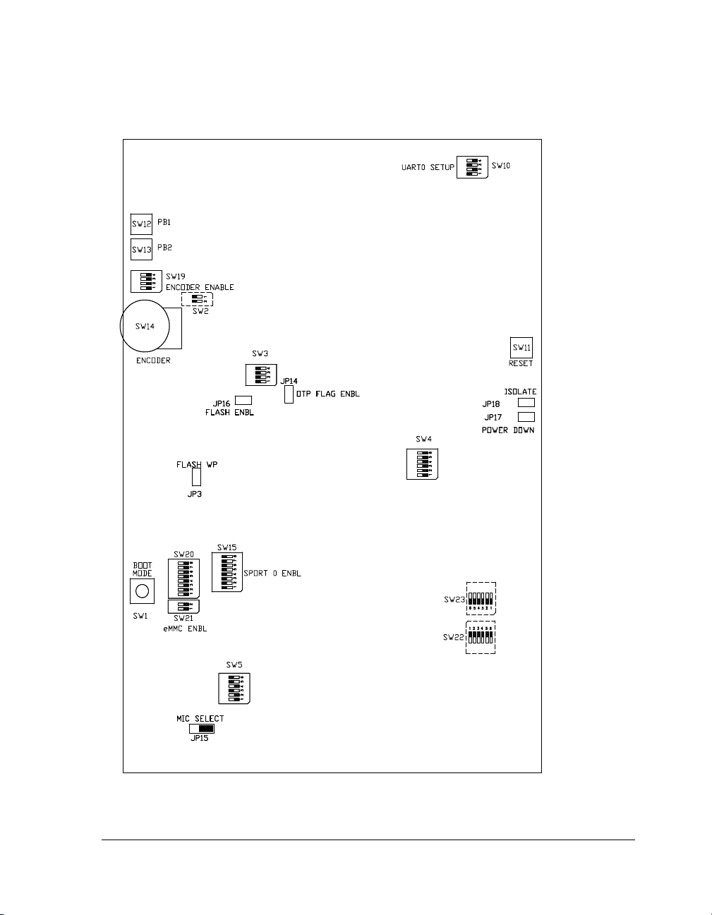
This section describes operation of the push buttons and switches. The
push button and switch locations are shown in Figure 2-2.
Figure 2-2. Push Button and Switch Locations
ADSP-BF518F EZ-Board Evaluation System Manual 2-7

Push Button and Switch Settings
Boot Mode Select Switch (SW1)
The boot mode select switch (SW1) determines the boot mode of the processor. Table 2-4 shows the available boot mode settings. By default, the
ADSP-BF518F processor boots from the on-board parallel flash memory.
L
entire rotating portion of the switch, not the small arrow.
Table 2-4. Boot Mode Select Switch (SW1)
The selected position of SW1 is marked by the notch down the
SW1 Position Processor Boot Mode
0 Reserved
1 Boot from 8- or 16-bit external flash memory (default)
2 Boot from 16-bit asynchronous FIFO
3 Boot from serial SPI memory
4 Boot from SPI host device
5 Boot from serial TWI memory
6 Boot from TWI host
7Boot from UART0 host
PB Enable Switch (SW2)
The PB enable switch (SW2) disconnects the associated push buttons from
the GPIO pins of the processor and allows the signals to be used for other
purposes (see Table 2-5).
2-8 ADSP-BF518F EZ-Board Evaluation System Manual

ADSP-BF518F EZ-Board Hardware Reference
Table 2-5. Push Button Enable Switch (SW2)
SW2 Position (Default) From To Function
1 (ON) Push button 1 (SW12)Processor
(U12, PH0)
2 (ON) Push button 2 (SW13)Processor
U12, PH1)
(
ON (PB1)
OFF (ADC DR1PRI, eMMC,
expansion interface II)
ON (PB2)
OFF (ADC RFS1, eMMC,
expansion interface II)
Flash Enable Switch (SW3)
The flash enable switch (SW3) disconnects the ~AMSx signals from parallel
flash memory (U5) and allows other devices to utilize the signals via the
expansion interface II. For each switch listed in Table 2-6 that is turned
OFF, the size of available flash memory is reduced by 1 MB. ~AMS3 is shared
with ~SPI0_SEL2 of the external SPI flash. When using the external SPI
flash, the available size for parallel flash is 3 MB.
Table 2-6. Flash Enable Switch (SW3)
SW3 Switch Position (Default) Processor Signal
1 (ON) ~AMS0
2 (ON) ~AMS1
3 (ON) ~AMS2
4 (ON) ~AMS3
SPORT1 Enable Switch (SW4)
The SPORT1 enable switch (SW4) connects the SPORT1 interface of the processor to the ADC7266 (
range of the ADC to either 2.5V (ON) or 5V (OFF). SW4 position 6 is used
ADSP-BF518F EZ-Board Evaluation System Manual 2-9
U2) device. SW4 position 5 is used to set the input

Push Button and Switch Settings
to configure the inputs for single-ended mode (
OFF) or differential mode
(ON). When the SPORT1 interface is used on the expansion interface II, set
SW4 to all OFF. SW4 is set to all OFF by default.
The SPORT1 interface is shared with other on-board components, such as
the eMMC device and push buttons.
MIC Gain/Loopback Switch (SW5)
The microphone gain switch (SW5) sets the gain of the MIC signal, which is
connected to the top 3.5 mm jack (J5). The gain can be set to 14 dB,
0 dB, or –6 dB by turning position 1, 2, or 3 of SW5 ON (see Table 2-7).
When the corresponding position for the desired gain is ON, the remaining
positions must be OFF. SW5 position 4 is used to connect the MICIN signal
to the right headphone output for loopback testing during a POST.
SW5 positions 5 and 6 are used to connect line-out to line-in for loopback
testing in a POST, when no cables are connected to J4 and J5. Refer to
“Audio Interface” on page 1-16 for more information about the audio
codec.
Table 2-7. MIC Gain Switch (SW5)
Gain SW5 Switch Settings
5 (14 dB) ON, OFF, OFF, OFF
1 (0 dB) OFF, ON, OFF, OFF
0.5 (–6 dB) OFF, OFF, ON, OFF (default)
Unused
OFF, OFF, OFF, OFF
UART Setup Switch (SW10)
The UART setup switch (SW10) configures the UART0 signals from the
GPIO pins of the processor. Position 4 is used to place the UART0 port of
the processor in a loopback condition. The jumper connects the
2-10 ADSP-BF518F EZ-Board Evaluation System Manual
UART0_TX

ADSP-BF518F EZ-Board Hardware Reference
line of the processor to the
UART0_RX signal of the processor. This is
required when a POST program is run to test the serial port interface. By
default, SW10 is ON, OFF, ON, OFF.
Reset Push Button (SW11)
The reset push button (SW11) resets the following ICs.
• Processor (
The reset push button does not reset the following ICs.
• SDRAM (
• Audio codec (U1), UART0 (U21), schmitt trigger hex inverter (U6)
•Digipot (U7), power (VR1—5)
The reset push button does not reset the standalone debug agent once the
debug agent is connected to a personal computer (PC). After communication between the debug agent and PC is initialized, pushing a reset button
does not reset the USB chip on the debug agent. The only way to reset the
USB chip on the debug agent is to power down the EZ-Board.
U12), parallel flash (U5), and Ethernet IC (U4)
U14), eMMC (U16)
Programmable Flag Push Buttons (SW12–13)
Two momentary push buttons (SW12 and SW13) are provided for general-purpose user input. The buttons connect to the
pins of the processor. The push buttons are active high and, when pressed,
send a high (
1) to the processor. The GPIO enable switch (SW2) discon-
nects the push buttons from the corresponding push button signals. Refer
to “PB Enable Switch (SW2)” on page 2-8 for more information.
ADSP-BF518F EZ-Board Evaluation System Manual 2-11
PH0 and PH1 GPIO

Push Button and Switch Settings
Rotary Encoder with Momentary Switch (SW14)
The rotary encoder (SW14) can be turned clockwise for an up count or
counter-clockwise for a down count. The encoder also features a momentary switch, activated by pushing the switch towards the processor, which
resets the counter to zero. The rotary encoder is a two-bit quadrature (gray
code) encoder. Refer to the Rotary Counter section of the ADSP-BF51x
Blackfin Processor Hardware Reference for more information.
The rotary encoder is disconnected from the processor by setting SW19
positions 1, 2, and 3 to OFF. See “Encoder Enable Switch (SW19)” on
page 2-12 for more information.
SPORT0 ENBL Switch (SW15)
The SPORT0 enable switch (SW15) connects the SPORT0 interface of the processor to the audio codec, SSM2603 (U1). SW15 positions 7 and 8 are used
to disconnect the TWI bus from the codec. When the SPORT0 interface is
used on the expansion interface II, set SW15 all OFF. By default, SW15 is set
to all ON.
Encoder Enable Switch (SW19)
The encoder enable switch (SW19) disconnects the rotary encoder signals
from the GPIO pins of the processor.
disable the SD card detect signals: pin
inserted into the SD connector. When
signals can be used on the expansion interface II (see Table 2-8).
Table 2-8. Encoder Enable Switch (SW19)
SW19 Position (Default) From To
1 (OFF)Encoder (SW14)Processor (U1, PH4)
2 (OFF)Encoder (SW14)Processor (U1, PH5)
2-12 ADSP-BF518F EZ-Board Evaluation System Manual
SW19 position 4 is used to enable or
PF14 determines whether a card is
SW19 is OFF, its associated GPIO

ADSP-BF518F EZ-Board Hardware Reference
Table 2-8. Encoder Enable Switch (SW19) (Cont’d)
SW19 Position (Default) From To
3 (OFF)Encoder (SW14)Processor (U1, PH6)
4 (OFF) SD connector (J13)Processor (U1, PF13)
eMMC Enable Switch (SW20–21)
The eMMC enable switches (SW20 and SW21) connect the RSI signals to
the on-board eMMC memory device. The eMMC and SD interfaces share
the same signals; therefore, no card should be inserted into the SD connector when the eMMC device is used. The default for the switches is all
OFF so that the SD connector can be used.
ADC Loopback Switches (SW22–23)
The ADC loopback switches (SW22 and SW23) are used for testing only.
The switches are used to send an analog signal generated from the codec to
the ADC circuit for evaluation.
ADSP-BF518F EZ-Board Evaluation System Manual 2-13

Jumpers
Jumpers
This section describes functionality of the configuration jumpers.
Figure 2-2 shows the jumper locations.
Figure 2-3. Configuration Jumper Locations
2-14 ADSP-BF518F EZ-Board Evaluation System Manual

ADSP-BF518F EZ-Board Hardware Reference
Flash WP Jumper (JP3)
The flash WP jumper (JP3) is used to write-protect block 70 of the parallel flash chip. Block 70 contains 64 KB of configuration data at address
range 0x203 F0000—0x203 FFFFF. When the jumper is installed on JP3,
and the parallel flash driver from Analog Devices is used, block 70 is
read-only. By default, JP3 is installed.
OTP Flag Enable Jumper (JP14)
The OTP flag enable jumper (JP14) controls the precise 7V OTP voltage
regulator. By default, JP14 is not installed; when installed, the jumper
allows OTP writes.
JP14 must be installed for OTP writes to be successful. The nominal 2.5V
for OTP is temporarily raised to 7V when PH3 is set high. Care must be
taken when using the OTP_FLAG signal in order to avoid driving 7V for an
extended amount of time.
a
Configured properly, JP14 connects the processor’s PH3 flag pin to the
shut-down pin of the ADP1611 switching converter. Refer to the
ADSP-BF51x Blackfin Processor Hardware Reference Manual and the
ADSP-BF512/ADSP-BF514/ADSP-BF516/ADSP-BF518 Blackfin Embedded Processor data sheet for more information about OTP writes.
ADSP-BF518F EZ-Board Evaluation System Manual 2-15
There is a limited amount of time 7V can be applied to the processor’s OTP interface. Violating the specifications listed in the
ADSP-BF512/ADSP-BF514/ADSP-BF516/ADSP-BF518 Blackfin
Embedded Processor data sheet can damage the processor.

Jumpers
MIC Select Jumper (JP15)
The microphone select jumper (JP15) connects the MICBIAS signal to the
MICIN signal (JP15 on positions 1&2) or connects the MICBIAS signal to
the 3.5 mm connector J5 (JP15 on positions 2&3). By default, JP15 is
installed on positions 2&3.
SPI FLASH CS Enable Jumper (JP16)
The SPI flash CS enable jumper (JP16) connects the SPI0_SSEL2 signal to
the SPI flash memory. When installing JP16, position 3 of SW3 needs to be
turned OFF since the SPI0_SSEL2 signal is shared with the ~AMS3 signal
connected to parallel flash. When using SPI flash, the available memory
that is accessible on parallel flash is reduced from 4 MB to 3 MB. By
default, JP16 is not installed, and SPI flash is not connected.
Ethernet Power Down Jumper (JP17)
The Ethernet power down jumper (JP17) is used to put the PHY device in
power-down mode, where the entire chip is powered down.
Ethernet Isolate Jumper (JP18)
The Ethernet isolate jumper (JP18) is used to put the the PHY device in
isolate mode. When in isolate mode, the PHY port is isolated from the
media independent interface (MII) of the ADSP-BF518F processor.
VDDINT Power Jumper (P8)
The VDDINT power jumper (P8) is used to measure voltage and current
supplied to the processor core. By default,
through the two-pin IDC header. To measure power, remove the jumper
2-16 ADSP-BF518F EZ-Board Evaluation System Manual
P8 is ON, and the power flows

ADSP-BF518F EZ-Board Hardware Reference
on
P8 and measure voltage across the 0.1 ohm resistor. Once voltage is
measured, power can be calculated. For more information, refer to “Power
Measurements” on page 1-23.
VDDEXT Power Jumper (P9)
The VDDEXT power jumper (P9) is used to measure the processor’s I/O
voltage and current. By default,
two-pin IDC header. To measure power, remove the jumper on
P9 is ON, and the power flows through the
P9 and
measure voltage across the 0.1 ohm resistor. Once voltage is measured,
power can be calculated. For more information, refer to “Power Measure-
ments” on page 1-23.
VDDMEM Power Jumper (P10)
The VDDMEM power jumper (P10) is used to measure voltage and current supplied to the memory interface of the processor. By default, P10 is
ON, and the power flows through the two-pin IDC header. To measure
power, remove the jumper on P10 and measure voltage across the 0.1 ohm
resistor. Once voltage is measured, power can be calculated. For more
information, refer to “Power Measurements” on page 1-23.
VDDFLASH Power Jumper (P11)
The VDDFLASH power jumper (P11) is used to measure flash voltage and
current supplied to the processor core. By default,
flows through the two-pin IDC header. To measure power, remove the
jumper on
P11 and measure voltage across the 0.1 ohm resistor. Once
voltage is measured, power can be calculated. For more information, refer
to “Power Measurements” on page 1-23.
ADSP-BF518F EZ-Board Evaluation System Manual 2-17
P11 is ON, and the power

LEDs
LEDs
This section describes the on-board LEDs. Figure 2-4 shows the LED
locations.
Figure 2-4. LED Locations
2-18 ADSP-BF518F EZ-Board Evaluation System Manual

ADSP-BF518F EZ-Board Hardware Reference
GPIO LEDs (LED1–3)
Three LEDs connect to three general-purpose I/O pins of the processor
(see Table 2-9). The LEDs are active high and lit by writing a ‘1’ to the
correct programmable flag signal.
Table 2-9. GPIO LEDs
LED Reference Designator Processor Programmable Flag Pin
LED1 PH3
LED2 PH5
LED3 PH6
Reset LED (LED9)
When LED9 is lit, it indicates that the master reset of all major ICs is
active. The reset LED is controlled by the Analog Devices ADM708
supervisory reset circuit. You can assert the reset push button (SW11) to
assert a master reset and activate LED9. For more information, see “Reset
Push Button (SW11)” on page 2-11.
Power LED (LED13)
When LED13 is lit solid, it indicates that the board is powered.
Speed LED (LED14)
When LED14 is lit, the Ethernet PHY device operates at 100 Mbs. When
the LED is OFF, the PHY device operates at 10 Mbs.
ADSP-BF518F EZ-Board Evaluation System Manual 2-19

Connectors
Connectors shown with a dotted line are on the backside of the PCB
Connectors
This section describes connector functionality and provides information
about mating connectors. The connector locations are shown in Figure 2-5.
Figure 2-5. Connector Locations
2-20 ADSP-BF518F EZ-Board Evaluation System Manual

ADSP-BF518F EZ-Board Hardware Reference
Expansion Interface II Connector (J1)
J1 is a board-to-board connector providing signals from the external bus
interface unit (EBIU) of the processor. The connector is located on the
left edge of the board. For more information, see “Expansion Interface II”
on page 1-22. For availability and pricing of the connector, contact
Samtec.
Part Description Manufacturer Part Number
104-position 0.025”, SMT header SAMTEC QMS-052-11-L-D-A
Mating Connector
104-position 0.025”, SMT socket SAMTEC QFS-052-01-L-D-A
RS-232 Connector (J2)
Part Description Manufacturer Part Number
DB9, female, vertical mount NORCOMP 191-009-213-L-571
Mating Cable
2m female-to-female cable DIGI-KEY AE1020-ND
Power Connector (J3)
The power connector (J3) provides all of the power necessary to operate
the EZ-Board.
Part Description Manufacturer Part Number
0.65 mm power jack CUI 045-0883R
Mating Power Supply (shipped with the EZ-Board)
5.0VDC@2.5A power supply CUI STACK DMS050260-P12P-SZ
ADSP-BF518F EZ-Board Evaluation System Manual 2-21

Connectors
Dual Audio Connectors (J4–5)
Part Description Manufacturer Part Number
3.5 mm dual stereo jack SWITCHCRAFT 35RAPC7JS
Mating Cable (shipped with the EZ-Board)
3.5 mm male/male 6’ cable RANDOM 10A3-01106
Battery Holder (J12)
Part Description Manufacturer Part Number
16 mm battery holder MEMORY PROTECTION BH600
Mating Battery (shipped with the EZ-Board)
3V 125MAH 16 mm LI-COIN PANASONIC CR1632
SD Connector (J13)
Part Description Manufacturer Part Number
SD 9-pin connector ITT CANON CCM05-5777LFT T50
Mating Memory Card (shipped with the EZ-Board)
256 MB SANDISK STACK SDSDB-256-A10
Ethernet Connectors (J14–15)
Part Description Manufacturer Part Number
RJ-45 Ethernet jack STEWART SS-6488-NF
Mating Cable (shipped with the EZ-Board)
Cat 5E patch cable RANDOM PC10/100T-007
2-22 ADSP-BF518F EZ-Board Evaluation System Manual

ADSP-BF518F EZ-Board Hardware Reference
JTAG Connector (P1)
The JTAG header is the connecting point for the JTAG interface to the
ADSP-BF518F processor. The standalone debug agent requires both connectors P1 and ZP1.
Pin 3 is missing to provide keying. Pin 3 in the mating connector should
have a plug.
When using an emulator with the EZ-Board, the standalone debug agent
must be removed. Follow the installation instructions provided in
“EZ-Board Installation” on page 1-4, using P1 as the JTAG connection
point.
Expansion Interface II Connectors (P2 and P4)
P2 and P4 are board-to-board connectors providing signals for the SPI,
TWI, UART, SPORT interfaces and GPIO signals of the processor. The
connectors are located on the upper and lower edges of the board. For
more information, see “Expansion Interface II” on page 1-22. For availability and pricing of the connectors, contact Samtec.
Part Description Manufacturer Part Number
50-position 0.1”, SMT header SAMTEC TSSH-125-01-L-DV-A
Mating Connector
50-position 0.1”, SMT socket SAMTEC SSW-125-22-F-D-VS
Expansion Interface II Connector (P3)
P3 is a board-to-board connector providing signals for the PPI, TWI, and
GPIO signals of the processor. The connector is located on the upper edge
of the board. For more information, see “Expansion Interface II” on
page 1-22. For availability and pricing of the connector, contact Samtec.
ADSP-BF518F EZ-Board Evaluation System Manual 2-23

Connectors
Part Description Manufacturer Part Number
70-position 0.1”, SMT header SAMTEC TSSH-135-01-L-DV-A
Mating Connector
70-position 0.1”, SMT socket SAMTEC SSW-135-22-F-D-VS
DMAX Land Grid Array Connectors (P5–7)
The land grid array areas (P5—7) are intended for the probing of the processor signals. The pads are exposed and designed to attach a Tektronix
logic analyzer to the connectors listed in the following table. For more
information about the land grid array, consult the Tektronix Web site.
Part Description Manufacturer Part Number
Primary retention TEKTRONIX 020290800
Alternate retention TEKTRONIX 020291000
Standalone Debug Agent Connector (ZP1)
ZP1 connects the standalone debug agent to the EZ-Board. The standalone
debug agent requires both the ZP1 and P1 connectors. For more informa-
tion, see “EZ-Board Installation” on page 1-4.
2-24 ADSP-BF518F EZ-Board Evaluation System Manual

A ADSP-BF518F EZ-BOARD
BILL OF MATERIALS
The bill of materials corresponds to “ADSP-BF518F EZ-Board Schematic” on
page B-1.
Ref. Qty. Description Reference
Designator
1174LVC14A
SOIC14
2 1 IDT74FCT3244A
PY SSOP20
3 1 32.768KHZ
OSC008
4 1 25MHZ OSC003 U19 EPSON SG-8002CA MP
5 4 SN74LVC1G08
SOT23-5
6 1 MT48LC32M16A
2TG-75 TSOP54
7 1 SI4411DY SO-8 U8 VISHAY Si4411DY-T1-E3
8 2 HX1188 ICS007 U27-28 DIGI-KEY 553-1340-ND
9 1 12MHZ OSC003 U20 EPSON SG-8002CA-MP
10 1 SN74AUC1G00
SOT23-5
11 1 KS8893M
PQFP128
U6 TI 74LVC14AD
U10 IDT IDT74FCT3244APYG
U3 EPSON MC-156-32.7680KA-A0:
U23-26 TI SN74LVC1G08DBVR
U14 MICRON MT48LC32M16A2P-75
U13 TI SN74AUC1G00DBVR
U4 MICREL KSZ8893MQL
Manufacturer Part Number
ROHS
12 1 BF518 M25P16
“U9”
U9 ST MICRO M25P16-VMW6G
ADSP-BF518F EZ-Board Evaluation System Manual A-1

Ref. Qty. Description Reference
Designator
Manufacturer Part Number
13 1 BF518
M29W320EB
"U5"
14 1 MTFC2GDKDM
FBGA169
15 1 ADM708SARZ
SOIC8
16 1 ADM3202ARNZ
SOIC16
17 1 ADSP-BF518F
LQFP176
18 1 ADP1864AUJZ
SOT23-6
19 1 ADP1611
MSOP8
20 1 ADP1715
MSOP8
21 1 ADP1710 TSOT5 VR3 ANALOG
22 1 ADR550B
SOT23-3
U5 STMICRO M29W320EB70ZE6E
U16 MICRON MTFC2GDKDM-WT
U22 ANALOG
DEVICES
U21 ANALOG
DEVICES
U12 ANALOG
DEVICES
VR1 ANALOG
DEVICES
VR6 ANALOG
DEVICES
VR5 ANALOG ADP1715ARMZ-R7
DEVICES
U11 ANALOG
DEVICES
ADM708SARZ
ADM3202ARNZ
ADSP-BF518BSWZ-4F4
ADP1864AUJZ-R7
ADP1611ARMZ-R7
ADP1710AUJZ-R7
ADR550BRTZ-REEL7
23 1 AD5258
MSOP10
24 1 SSM2602 ICS009 U1 ANALOG
25 1 ADP1715
MSOP8
26 6 AD8022 MSOP8 U29-34 ANALOG
27 1 AD7266
LFCSP32
U7 ANALOG
DEVICES
DEVICES
VR4 ANALOG
DEVICES
DEVICES
U2 ANALOG
DEVICES
AD5258BRMZ10
SSM2602CPZ-R2
ADP1715ARMZ-1.8R7
AD8022ARMZ
AD7266BCPZ
A-2 ADSP-BF518F EZ-Board Evaluation System Manual

ADSP-BF518F EZ-Board Bill Of Materials
Ref. Qty. Description Reference
Designator
28 1 ADP1610
MSOP8
29 1 DIP3 SWT015 SW19 DIGI-KEY CKN6114-ND
30 1 DIP8 SWT016 SW20 C&K TDA08H0SB1
31 6 DIP6 SWT017 SW15-18,SW22-23CTS 218-6LPST
32 7 DIP4 SWT018 SW3-8,SW10 ITT TDA04HOSB1
33 12 SMA XPINS
CON043
34 1 DB9 9PIN
CON038
35 2 DIP2 SWT020 SW2,SW21 C&K CKN9064-ND
36 4 IDC 2X1
IDC2X1
37 5 IDC 2X1
IDC2X1
38 13 IDC 3X1
IDC3X1
VR2 ANALOG
J7,J16-26 JOHNSON
J2 NORCOMP 191-009-213-L-571
P8-11 FCI 90726-402HLF
JP3,JP11-14 FCI 90726-402HLF
JP15,JP17-28 FCI 90726-403HLF
Manufacturer Part Number
ADP1610ARMZ-R7
DEVICES
142-0701-201
COMP
39 1 3A RESETABLE
FUS004
40 24 IDC
2PIN_JUMPER_
SHORT
41 1 PWR .65MM
CON045
42 2 3.5MM
DUAL_STEREO
CON050
43 1 SD_CONN 9PIN
CON051
F1 TYCO SMD300F-2
SJ1-24 DIGI-KEY S9001-ND
J3 CUI 045-0883R
J4-5 SWITCHCRAFT 35RAPC7JS
J13 DIGI-KEY 401-1954-ND
ADSP-BF518F EZ-Board Evaluation System Manual A-3

Ref. Qty. Description Reference
Designator
Manufacturer Part Number
44 2 RJ45 8PIN
CON_RJ45_12P
45 3 MOMENTARY
SWT024
46 1 ROTARY_ENC_
EDGE SWT025
47 1 QMS 52x2
QMS52x2_SMT
48 2 IDC 25x2
IDC25x2_SMTA
49 1 IDC 35x2
IDC35x2_SMTA
50 1 IDC 7x2
IDC7x2_SMTA
51 1 BATT_HOLDER
16MM
BATT_COI
52 2 IDC 2X1
IDC2X1_SMT
53 1 ROTARY
SWT027
J14-15 DIGI-KEY 380-1022-ND
SW11-13 PANASONIC EVQ-Q2K03W
SW14 PANASONIC EVQ-WKA001
J1 SAMTEC QMS-052-06.75-L-D-A
P2,P4 SAMTEC TSSH-125-01-L-DV-A
P3 SAMTEC TSSH-135-01-L-DV-A
P1 SAMTEC TSM-107-01-T-DV-A
J12 MEMORY PRO-
TECTI
JP4,JP16 SAMTEC TSM-102-01-T-SV
SW1 COPAL S-8010
BH600
54 3 YELLOW
LED001
55 2 100 1/10W 5%
0805
56 11 600 100MHZ
200MA 0603
57 2 600 100MHZ
500MA 1206
58 2 10UF 16V 20%
CAP002
LED1-3 PANASONIC LN1461C
R165,R167 VISHAY CRCW0805100RJNEA
FER2-9,FER12-14DIGI-KEY 490-1014-2-ND
FER15-16 STEWARD HZ1206B601R-10
CT1-2 PANASONIC EEE1CA100SR
A-4 ADSP-BF518F EZ-Board Evaluation System Manual

ADSP-BF518F EZ-Board Bill Of Materials
Ref. Qty. Description Reference
Designator
59 1 0 1/10W 5% 0805 R69 VISHAY CRCW08050000Z0EA
60 1 190 100MHZ 5A
FER002
61 8 YELLOW
LED009
62 2 0.47UF 16V 10%
0805
63 2 1UF 10V 10%
0805
64 18 10UF 6.3V 10%
0805
65 1 4.7UF 6.3V 10%
0805
66 47 0.1UF 10V 10%
0402
FER17 MURATA DLW5BSN191SQ2
LED4-8,LED10-12PANASONIC LNJ416Q8YRA
C59-60 AVX 0805YC474KAT2A
C123-124 AVX 0805ZC105KAT2A
C7,C10,C1516,C37,C41,C61,
C64,C66,C71,
C75,C88,C90,
C94-95,C98,
C101,C106
C145 AVX 08056D475KAT2A
C4-6,C9,C1114,C25,C39,C4245,C47-48,C6263,C65,C72,C76,
C86-87,C89,
C108-110,C113,
C115-118,C140,
C152,C188-194,
C211-216
Manufacturer Part Number
AVX 08056D106KAT2A
AVX 0402ZD104KAT2A
67 59 0.01UF 16V 10%
0402
C1,C8,C17-24,
C26-36,C38,C46,
C49-58,C73,C9293,C96-97,C99100,C102-105,
C119-122,C139,
C154,C179-187
AVX 0402YC103KAT2A
ADSP-BF518F EZ-Board Evaluation System Manual A-5

Ref. Qty. Description Reference
Designator
Manufacturer Part Number
68 48 10K 1/16W 5%
0402
69 9 4.7K 1/16W 5%
0402
70 27 0 1/16W 5% 0402 R9,R202,R205-
71 10 22 1/16W 5%
0402
72 3 33 1/16W 5%
0402
R1,R11,R18-21,
R26,R56-59,R8587,R89,R106108,R110-115,
R117,R143-145,
R152,R154-156,
R161-164,R168,
R170-173,R203,
R245,R268,R270,
R353-355
R6-8,R13-17,
R269
206,R209-212,
R214-215,R217218,R221-222,
R224-225,R227228,R230-233,
R235-236,R238239,R267
R146-151,R241244
R313-314,R325 VISHAY CRCW040233R0JNEA
VISHAY CRCW040210K0FKED
VISHAY CRCW04024K70JNED
PANASONIC ERJ-2GE0R00X
PANASONIC ERJ-2GEJ220X
73 7 33 1/16W 5%
0402
74 2 18PF 50V 5%
0805
75 2 2.2UF 10V 10%
0805
76 24 10PF 50V 5%
0805
77 2 0.1UF 16V
10%0603
R3,R12,R60,R6667,R78,R199
C2-3 AVX 08055A180JAT2A
C150-151 AVX 0805ZD225KAT2A
C155-178 AVX 08055A100JAT2A
C40,C136 AVX 0603YC104KAT2A
VISHAY CRCW040233R0JNEA
A-6 ADSP-BF518F EZ-Board Evaluation System Manual

ADSP-BF518F EZ-Board Bill Of Materials
Ref. Qty. Description Reference
Designator
78 5 1UF 16V 10%
0603
79 1 68PF 50V 5%
0603
80 3 4.7UF 6.3V 20%
0603
81 1 470PF 50V 5%
0603
82 3 220UF 6.3V 20%
D2E
83 1 10M 1/10W 5%
0603
84 5 330 1/10W 5%
0603
85 4 0 1/10W 5% 0603 R52-53,R195,
86 34 49.9 1/16W 1%
0603
C79-81,C199,
C208
C144 AVX 06035A680JAT2A
C137-138,C141 PANASONIC ECJ-1VB0J475M
C143 AVX 06033A471JAT2A
CT3-4,CT6 SANYO 10TPE220ML
R10 VISHAY CRCW060310M0FNEA
R153,R157-160 VISHAY CRCW0603330RJNEA
R346
R68,R71-77,R7984,R118-126,
R128-135,R137139
Manufacturer Part Number
PANASONIC ECJ-1VB1C105K
PHYCOMP 232270296001L
VISHAY CRCW060349R9FNEA
87 15 10 1/10W 5%
0603
88 1 10.0K 1/10W 1%
0603
89 8 100PF 50V 5%
0603
90 1 1000PF 50V 5%
0603
R166,R169,R207208,R213,R216,
R219-220,R223,
R226,R229,R234,
R237,R240,R349
R183 DIGI-KEY 311-10.0KHRTR-ND
C67-70,C82-85 AVX 06035A101JAT2A
C207 PANASONIC ECJ-1VC1H102J
VISHAY CRCW060310R0JNEA
ADSP-BF518F EZ-Board Evaluation System Manual A-7

Ref. Qty. Description Reference
Designator
Manufacturer Part Number
91 1 2200PF 50V 5%
0603
92 2 75.0 1/10W 1%
0603
93 3 100 1/16W 5%
0402
94 1 4.99K 1/16W 1%
0603
95 1 24.9K 1/10W 1%
0603
96 3 511.0 1/16W 1%
0402
97 2 10UF 10V 10%
0805
98 1 2.0K 1/16W 1%
0603
99 6 0.05 1/2W 1%
1206
100 11 10UF 16V 10%
1210
C130 PANASONIC ECJ-1VB1H222K
R127,R136 DALE CRCW060375R0FKEA
R49,R54,R70 DIGI-KEY 311-100JRTR-ND
R347 VISHAY CRCW06034K99FKEA
R192 DIGI-KEY 311-24.9KHTR-ND
R140-142 DIGI-KEY 311-511LCT-ND
C107,C111 PANASONIC ECJ-2FB1A106K
R182 PANASONIC ERJ-3EKF2001V
R190-191,R194,
R196,R198,R204
C125-127,C135,
C146,C149,C200
-203,C205
SEI CSF 1/2 0.05 1%R
AVX 1210YD106KAT2A
101 1 GREEN LED001 LED13 PANASONIC LN1361CTR
102 1 RED LED001 LED9 PANASONIC LN1261CTR
103 2 1000PF 50V 5%
1206
104 1 255.0K 1/10W
1% 0603
105 1 80.6K 1/10W 1%
0603
106 8 270 1/10W 5%
0603
C147-148 AVX 12065A102JAT2A
R197 VISHAY CRCW06032553FK
R193 DIGI-KEY 311-80.6KHRCT-ND
R95-102 PANASONIC ERJ-3GEYJ271V
A-8 ADSP-BF518F EZ-Board Evaluation System Manual

ADSP-BF518F EZ-Board Bill Of Materials
Ref. Qty. Description Reference
Designator
107 2 22000PF 25V
10% 0402
108 2 5A
MBRS540T3G
SMC
109 1 20MA
MA3X717E
DIO005
110 1 2.5UH 30%
IND013
111 1 33.0K 1/16W 1%
0402
112 5 47.0K 1/16W 1%
0402
113 1 3.01K 1/16W 1%
0402
114 1 5.6K 1/16W 5%
0402
115 15 1.0K 1/16W 1%
0402
C131,C197 DIGIKEY 490-3252-1-ND
D7-8 ON SEMI MBRS540T3G
D1 PANASONIC MA3X717E
L3 COILCRAFT MSS1038-252NLB
R201 ROHM MCR01MZPF3302
R46,R48,R5051,R55
R63 ROHM MCR01MZPF3011
R247 PANASONIC ERJ-2GEJ562X
R61-62,R64-65,
R88,R91,R93-94,
R103,R105,R109,
R116,R189,R271272
Manufacturer Part Number
ROHM MCR01MZPF4702
PANASONIC ERJ-2RKF1001X
116 2 1000PF 2000V
10% 1206
117 3 220PF 50V 10%
0402
118 4 5.6K 1/16W 0.5%
0402
119 1 680 1/16W 1%
0402
C112,C114 AVX 1206GC102KAT1A
C153,C195-196 DIGI-KEY 311-1035-2-ND
R40,R43-45 SUSUMU RR0510P-562-D
R42 BC COMPO-
NENTS
2312 275 16801
ADSP-BF518F EZ-Board Evaluation System Manual A-9

Ref. Qty. Description Reference
Designator
Manufacturer Part Number
120 1 90.9K 1/16W 5%
0402
121 1 40.2K 1/16W 5%
0402
122 2 100K 1/16W 5%
0402
123 4 2.2UF 25V 10%
0805
124 1 21.5K 1/10W 1%
0603
125 6 1A
MBR130LSFT1G
SOD-123FL
126 1 22UH 20%
IND018
127 3 1UH 20%
IND019
128 13 33 1/32W 5%
RNS005
129 3 1.2K 1/16W 1%
0402
R41 DIGI-KEY 541-90.9KLCT-ND
R47 DIGI-KEY 541-40.2KLCT-ND
R200,R350 DIGI-KEY 541-100KJTR-ND
C129,C132,
C204,C206
R179 DIGI-KEY 311-21.5KHRCT-ND
D2-5,D9-10 ON SEMI MBR130LSFT1G
L1 COILCRAFT MSS4020-223MLB
L2,L6-7 COILCRAFT ME3220-102MLB
RN4-13,RN17-19 PANASONIC EXB-28V330JX
R4-5,R186 PANASONIC ERJ-2RKF1201X
DIGIKEY 490-3331-1-ND
130 2 4.3 1/4W 5%
1206
131 1 2.67K 1/16W 1%
0402
132 3 1.0M 1/16W 1%
0402
133 2 22UH 20%
IND024
134 4 330 100MHZ
1.5A 0805
R185,R188 PANASONIC ERJ-8GEYJ4R3V
R187 PANASONIC ERJ-2RKF2671X
R248-250 VISHAY CRCW04021M00FKED
L8-9 COILCRAFT MSD7342-223MLC
FER1,FER19-21 MURATA BLM21PG331SN1D
A-10 ADSP-BF518F EZ-Board Evaluation System Manual

ADSP-BF518F EZ-Board Bill Of Materials
Ref. Qty. Description Reference
Designator
135 8 22 1/32W 5%
RNS005
136 1 3300PF 50V 5%
0603
137 1 24.0K 1/10W 1%
0603
138 1 140.0K 1/10W
1% 0603
139 1 44.2K 1/10W 1%
0603
140 1 1.91K 1/10W .1%
0603
141 1 3.01K 1/10W .1%
0603
142 1 20.0K 1/16W 1%
0402
RN1-3,RN14-16,
RN20-21
C198 PANASONIC ECJ-1VB1H332K
R176 PANASONIC ERJ-3EKF2402V
R181 PANASONIC ERJ-3EKF1403V
R348 PANASONIC ERJ-3EKF4422V
R180 SUSUMU RG1608P-1911-B-T5
R184 SUSUMU RG1608P-3011-B-T1
R344 VISHAY CRCW040220K0FKED
Manufacturer Part Number
PANASONIC EXB-28V220JX
ADSP-BF518F EZ-Board Evaluation System Manual A-11

A-12 ADSP-BF518F EZ-Board Evaluation System Manual

A B C
D
1
1
2
2
ADSP-BF518F EZ-BOARD
SCHEMATIC
3
ANALOG
4
DEVICES
20 Cotton Road
Nashua, NH 03063
PH: 1-800-ANALOGD
3
4
Title
ADSP-BF518F EZ-BOARD
TITLE
Size Board No.
C
Date Sheet of
A B C D
5-11-2009_10:44 1 15
A0217-2008
Rev
1.0

A B C
D
3.3V
A[1:19]_Z
A1_Z
A2_Z
A3_Z
A4_Z
A5_Z
1
SCKE_Z
SWE_Z
SA10_Z
SCAS_Z
SRAS_Z
2
TP10
3.3V
R1
10K
0402
SMS_Z
DSP_CLKIN
DSP_RTXI
DSP_RTXO
NMI
RESET
A6_Z
A7_Z
A8_Z
A9_Z
A10_Z
A11_Z
A12_Z
A13_Z
A14_Z
A15_Z
A16_Z
A17_Z
A18_Z
A19_Z
U12
107
A1
106
A2
105
A3
103
A4
102
A5
101
A6
97
A7
96
A8
94
A9
93
A10
92
A11
91
A12
86
A13
85
A14
84
A15
81
A16
80
A17
78
A18
77
A19
119
SCKE
113
SWE
110
SA10
114
SCAS
115
SRAS
118
SMS
143
CLKIN
144
XTAL
141
RTXI
140
RTXO
147
NMI
146
RESET
ADSP-BF518F
LQFP176_SOCKET
D0
D1
D2
D3
D4
D5
D6
D7
D8
D9
D10
D11
D12
D13
D14
D15
ABE1#/SDQM1
ABE0#/SDQM0
AMS1
AMS0
ARE
AWE
CLKOUT
TEST
PG
EXT_WAKE
NC
CLKBUF
76
74
73
72
71
70
69
66
65
64
62
61
60
58
57
56
108
109
120
123
121
122
125
117
135
130
127
150
D0_Z
D1_Z
D2_Z
D3_Z
D4_Z
D5_Z
D6_Z
D7_Z
D8_Z
D9_Z
D10_Z
D11_Z
D12_Z
D13_Z
D14_Z
D15_Z
TP9
D[0:15]_Z
ABE1#/SDQM1_Z
ABE0#/SDQM0_Z
AMS1_Z
AMS0_Z
ARE_Z
AWE_Z
R3
33
0402
R199
33
0402
CLKOUT
PG
WAKE
CLKBUF
AMS3/SPI0_SEL2
ETXD2
ERXD2
ETXD3
ERXD3
ERXCLK
ERXDV
COL
SPI0_SSEL1
MDC
MDIO
ETXD0
ERXD0
ETXD1
ERXD1
ETXEN
RMII_PHYINT
MIICRS/HWAIT
ERXER
MIITXCLK
DR0PRI/SD_D0_Z
RSCLK0/SD_D1_Z
RFS0/SD_D2_Z
TFS0/SD_D3_Z
DT0PRI/SD_CMD_Z
TSCLK0/SD_CLK_Z
UART0_TX_Z
UART0_RX_Z
AMS2_Z
SPI0_SCK_Z
SPI0_MISO_Z
SPI0_MOSI_Z
R325 33
0402
U12
19
PF0/ETXD2/PPID0/SPI1_SSEL2/TACLK6
18
PF1/ERXD2/PPID1/PWM_AH/TACLK7
13
PF2/ETXD3/PPID2/PWM_AL
12
PF3/ERXD3/PPID3/PWM_BH/TACLK0
11
PF4/ERXCLK/PPID4/PWM_BL/TACLK1
10
PF5/ERXDV/PPID5/PWM_CH/TACI0
6
PF6/COL/PPID6/PWM_CL/TACI1
5
PF7/SPI0_SSEL1/PPID7/PWM_SYNC
4
PF8/MDC/PPID8/SPI1_SSEL4
3
PF9/RMIIMDIO/PPID9/TMR2
174
PF10/ETXD0/PPID10/TMR3
171
PF11/ERXD0/PPID11/PWM_AH/TACI3
168
PF12/ETXD1/PPID12/PWM_AL
167
PF13/ERXD1/PPID13/PWM_BH
166
PF14/ETXEN/PPID14/PWM_BL
165
PF15/RMII_PHYINT/PPID15/PWM_SYNC
48
PG0/MIICRS/RMIICRS/HWAIT/SPI1_SSEL3
47
PG1/ERXER/DMAR1/PWM_CH
39
PG2/MIITXCLK/RMIIREF_CLK/DMAR0/PWM_CL
38
PG3/DR0PRI/RSI_DATA0/SPI0_SSEL5/TACLK3
37
PG4/RSCLK0/RSI_DATA1/TMR5/TACI5
36
PG5/RFS0/RSI_DATA2/PPICLK/TMRCLK
34
PG6/TFS0/RSI_DATA3/TMR0/PPIFS1
33
PG7/DT0PRI/RSI_CMD/TMR1/PPIFS2
32
PG8/TSCLK0/RSI_CLK/TMR6/TACI6
31
PG9/DT0SEC/UART0_TX/TMR4
28
PG10/DR0SEC/UART0_RX/TACI4
27
PG11/SPI0_SS/AMS[2]/SPI1_SSEL5/TACLK2
26
PG12/SPI0_SCK/PPICLK/TMRCLK
25
PG13/SPI0_MISO/TMR0/PPIFS1
21
PG14/SPI0_MOSI/TMR1/PPIFS2/PWM_TRIPB
20
PG15/SPI0_SSEL2/PPIFS3/AMS[3]
PJ0/SCL
PJ1/SDA
PH0/DR1PRI/SPI1_SS/RSI_DATA4
PH1/RFS1/SPI1_MISO/RSI_DATA5
PH2/RSCLK1/SPI1_SCK/RSI_DATA6
PH3/DT1PRI/SPI1_MOSI/RSI_DATA7
PH4/TFS1/AOE/SPI0_SSEL3/CUD
PH5/TSCLK1/ARDY/ECLK/CDG
PH6/DT1SEC/UART1_TX/SPI1_SSEL1/CZM
PH7/DR1SEC/UART1_RX/TMR7/TACI2
173
0402
R313 33
172
0402
162
161
160
159
156
155
154
153
R4
1.2K
0402
33R314
PB1/DR1PRI/MMC_D4_Z
PB2/RFS1/MMC_D5_Z
RSCLK1/MMC_D6_Z
ADC_A0/LED1/MMC_D7/OTP_EN_Z
CUD/SD_CD_Z
CDG/ADC_A1/LED2_Z
CZM/ADC_A2/LED3_Z
DR1SEC_Z
R5
1.2K
0402
1
SCL
SDA
2
"BOOT MODE"
1
3
2
4
4
5
R8
4.7K
0402
R6
4.7K
0402
20 Cotton Road
SW1
2
1
0
7
6
SWT027
ROTARY
3.3V
C
3
C153
220PF
0402
R202
0
0402
TDO
R9
0
0402
TRST
TMS
EMU
TCK
TDI
54
TRST
55
TMS
51
EMU
53
TCK
50
TDO
52
TDI
ADSP-BF518F
LQFP176_SOCKET
SW1: Boot Mode Select Switch
0
Default
1
2
3
4
5
6
7
BOOT MODEPOSITION
Idle-No Boot
Boot from 8 or 16-bit external flash memory
Boot from internal SPI memory
Boot from external SPI memory
Boot from SPI0 host
Boot from OTP memory
Boot from SDRAM
Boot from UART0 host
BMODE0
BMODE1
BMODE2
42
41
40
R7
4.7K
0402
ANALOG
3.3V
3.3V
R11
10K
4
3
0402
R10
10M
0603
U3
TERM1TERM2
NC1NC2
32.768KHZ
OSC008
4
U19
VDD
1 3
OE OUT
GND
2
25MHZ
OSC003
1
2
C3
18PF
0805
R12
33
0402
DSP_CLKIN
PG
3.3V
R200
100K
0402
R201
33.0K
0402
3
C1
0.01UF
0402
DSP_RTXI DSP_RTXO
C2
18PF
0805
Nashua, NH 03063
4
DEVICES
PH: 1-800-ANALOGD
4
RTC
Title
ADSP-BF518F EZ-BOARD
DSP EBIU + CONTROL
Size Board No.
C
Date Sheet of
A B C D
A0217-2008
Rev
1.0
155-11-2009_10:44 2

A B C
VDDEXT
D
1
VDDEXT
U12
7
VDDEXT1
24
VDDEXT2
35
VDDEXT3
49
VDDEXT4
128
VDDEXT5
129
VDDEXT6
136
VDDEXT7
145
VDDEXT8
148
VDDEXT9
158
VDDMEM
2
VDDINT
3.3V
VDDFLASH
VDDEXT10
170
VDDEXT11
59
VDDMEM1
68
VDDMEM2
75
VDDMEM3
82
VDDMEM4
95
VDDMEM5
104
VDDMEM6
112
VDDMEM7
124
VDDMEM8
14
VDDINT1
23
VDDINT2
30
VDDINT3
63
VDDINT4
79
VDDINT5
98
VDDINT6
100
VDDINT7
116
VDDINT8
138
VDDINT9
152
VDDINT10
164
VDDINT11
GND1
GND2
GND3
GND4
GND5
GND6
GND7
GND8
GND9
GND10
GND11
GND12
GND13
GND14
GND15
GND16
GND17
GND18
GND19
GND20
GND21
GND22
GND23
GND24
GND25
GND26
GND27
GND28
GND29
GND30
1
2
15
22
43
44
45
46
67
83
87
88
89
90
99
111
131
132
133
134
137
139
149
151
157
163
169
175
176
177
C7 C6
10UF
0805
VDDMEM
C10
10UF
0805
VDDINT
C15 C14
10UF
0805
C37 C38
10UF
0805
C16
10UF
0805
0.1UF
0402
0.1UF
0402
C9
0.1UF
0402
C13
0.1UF
0402
C5
0.1UF
0402
C25
0.1UF
0402
C12
0.1UF
0402
C4
0.1UF
0402
C19 C18
0.01UF
0402
C11
0.1UF
0402
C39
0.1UF
0402
0.01UF
0402 0402
C31 C30
0.01UF
0402
C8
0.01UF
0402
C20
0.01UF
0402
0.01UF
0402 0402
0.01UF
0402 0402
C17
0.01UF
C32
0.01UF
C23C22
0.01UF
C27 C26
0.01UF
0402
C29
0.01UF
C21
0.01UF
0.01UF
0402
C33
0.01UF
04020402
C24
0.01UF
04020402
C28
0.01UF
0402
0.01UF
0402
C36
0.01UF
0402
1
2
D1
MA3X717E
20MA
DIO005
J12
12
3
BATT_COIN16MM
BATTHOLDER
C34
0.01UF
0402
VPPOTP VDDOTP
"RTC BATTERY"
C40
0.1UF
0603
C35
0.01UF
0402
16
VDDFLASH1
17
VDDFLASH2
29
VDDFLASH3
126
VDDFLASH4
142
VDDRTC
9
VDDOTP
8
VPPOTP
ADSP-BF518F
LQFP176_SOCKET
VDDFLASH
10UF
0805
C42C41
0.1UF
0402
C43
0.1UF
0402
C44
0.1UF
0402
C45
0.1UF
0402
3
ANALOG
20 Cotton Road
Nashua, NH 03063
4
Title
DEVICES
ADSP-BF518F EZ-BOARD
PH: 1-800-ANALOGD
4
DSP POWER, BYPASS CAPS
Size Board No.
C
A0217-2008
Date Sheet of
A B C D
Rev
1.0
1535-11-2009_10:44

A B C
D
4 MB FLASH
64MB SDRAM (32M x 16)
(2M x 16)
3.3V
1
SW3: FLASH ENABLE
A[1:19]
FROM DEFAULT ALTERNATE FUNCTION / OFF MODEPOS.
1
2
3
4
2
DSP (U12)
DSP (U12)
DSP (U12)
DSP (U12)
R13
4.7K
0402
"FLASH ENBL"
SW3
AMS0
AMS1
AMS2
AMS3/SPI0_SEL2
1
2
3
4 5
1 2 3 4
DIP4
SWT018
RESET
ARE
AWE
ON
8
7
6
TO
FLASH (U5)
FLASH (U5)
FLASH (U5)
FLASH (U5)
3.3V
R14
R15
4.7K
4.7K
0402
0402
R16
4.7K
0402
ON
ON
ON
ON
Expansion Interface
Expansion Interface
Expansion Interface
Expansion Interface, SPI FLASH CS
R17
4.7K
0402
R269
4.7K
0402
U23
1
2
SN74LVC1G08
SOT23-5
U13
1
2
SN74AUC1G00
SOT23-5
U24
1
2
SN74LVC1G08
SOT23-5
4
U25
1
4
4
2
SN74LVC1G08
SOT23-5
4
A1
A2
A3
A4
A5
A6
A7
A8
A9
A10
A11
A12
A13
A14
A15
A16
A17
A18
A19
U5
G2
A0
F2
A1
E2
A2
C2
A3
D2
A4
F3
A5
E3
A6
C3
A7
D6
A8
C6
A9
E6
A10
F6
A11
D7
A12
C7
A13
E7
A14
F7
A15
G7
A16
D3
A17
E4
A18
F5
A19
F4
A20
D5
RESET
H7
BYTE
C4
RY/BY~
H2
CE
J2
OE
C5
WE
D4
VPP/WP~
M29W320EB
TFBGA63_80
J5
VDD
D0
D1
D2
D3
D4
D5
D6
D7
D8
D9
D10
D11
D12
D13
D14
D15/A-1
GND1
GND2
K2
K7
G3
K3
G4
K4
K5
G5
K6
G6
H3
J3
H4
J4
H5
J6
H6
J7
D0
D1
D2
D3
D4
D5
D6
D7
D8
D9
D10
D11
D12
D13
D14
D15
D[0:15]
3.3V
C54
0.01UF
0402
A[1:19]
SA10
SCAS
SRAS
ABE0#/SDQM0
ABE1#/SDQM1
SWE
3.3V
A1
A2
A3
A4
A5
A6
A7
A8
A9
A10
A12
A13
A18
A19
C47
0.1UF
0402
U14
23
A0
24
A1
25
A2
26
A3
29
A4
30
A5
31
A6
32
A7
33
A8
34
A9
22
A10
35
A11
36
A12_NC
20
BA0
21
BA1
16
WE
17
CAS
18
RAS
15
DQML
39
DQMH
MT48LC32M16A2TG-75
TSOP54
C48
0.1UF
0402
C49
0.01UF
0402
DQ10
DQ11
DQ12
DQ13
DQ14
DQ15
C50
0.01UF
0402
DQ0
DQ1
DQ2
DQ3
DQ4
DQ5
DQ6
DQ7
DQ8
DQ9
CS
CKE
CLK
2
4
5
7
8
10
11
13
42
44
45
47
48
50
51
53
19
37
38
D0_ZZ
D1_ZZ
D2_ZZ
D3_ZZ
D4_ZZ
D5_ZZ
D6_ZZ
D7_ZZ
D8_ZZ
D9_ZZ
D10_ZZ
D11_ZZ
D12_ZZ
D13_ZZ
D14_ZZ
D15_ZZ
C51
0.01UF
0402
R356
10K
0402
C52
0.01UF
0402
SMS
SCKE
CLKOUT
D[0:15]_ZZ
C53
0.01UF
0402
1
2
3
"FLASH WP"
3.3V
4
JP3
1
2
IDC2X1
MEMORY MAP
ADDRESS RANGE
0x2030 0000 - 0x203F FFFF
0x2020 0000 - 0x202F FFFF
0x2010 0000 - 0x201F FFFF
0x2000 0000 - 0x200F FFFF
0x0000 0000 - 0x03FF FFFF
C58
0.01UF
0402 0402
C57 C56
0.01UF
SJ1
SHORTING
JUMPER
DEFAULT=NOT INSTALLED
SELECT LINE TYPE
ASYNC BANK 3
ASYNC BANK 2
ASYNC BANK 1
ASYNC BANK 0
0.01UF
0402 0402
C55
0.01UF
FLASH
FLASH
FLASH
FLASH
NONE SDRAM
AMS3/SPI0_SEL2
"SPI FLASH CS ENBL"
3.3V
16 Mb SPI FLASH
R20R18
10K
10K
0402
0402
U9
SPI0_MOSI SPI0_MISO
SPI0_SCK
JP16
1 2
IDC2X1_SMT
SJ9
SHORTING
JUMPER
DEFAULT=NOT INSTALLED
R19
10K
0402
5
SI SO
6
SCK
1
CS
3
WP
7
HOLD
M25P16
SO8W
8
VCC
GND
4
2
3.3V
R21
10K
0402
C46
0.01UF
0402
ANALOG
DEVICES
20 Cotton Road
Nashua, NH 03063
PH: 1-800-ANALOGD
3
4
Title
ADSP-BF518F EZ-BOARD
EXTERNAL MEMORY
Size Board No.
C
Date Sheet of
A B C D
A0217-2008
Rev
1.0
4 155-11-2009_10:44

A B C
D
R367
10K
0402
R366
10K
0402
R210
0
0402
R212
0
0402
3
2
5
6
U33
AD8022
MSOP8
R209
0
0402
C156
10PF
0805
U33
AD8022
MSOP8
R211
0
0402
C158
10PF
0805
1
7
R208
10
0603
R213
10
0603
C157
10PF
0805
C159
10PF
0805
VA5
1
AGND
VA6
AGND
2
R214
0
0402
IN_VA1
R358
10K
0402
1
AGND
R217
0
0402
IN_VA2
R359
10K
0402
AGND
3
2
+12V;8
-12V;4
5
6
U29
AD8022
MSOP8
R215
0
0402
C161
10PF
0805
U29
AD8022
MSOP8
R218
0
0402
C163
10PF
0805
1
7
R216
10
0603
R219
10
0603
C160
10PF
0805
C162
10PF
0805
IN_VA3
VA1
AGND
AGND
IN_VA4
VA2
AGND
R362
10K
0402
R363
10K
0402
R222
0
0402
R225
0
0402
3
2
5
6
U31
AD8022
MSOP8
R221
0
0402
C164
10PF
0805
U31
AD8022
MSOP8
R224
0
0402
C166
10PF
0805
1
7
R220
10
0603
R223
10
0603
C165
10PF
0805
C167
10PF
0805
IN_VA5
VA3
AGND
AGND
IN_VA6
VA4
AGND
AGNDAGND
2
IN_VB1
AGND
R361
10K
0402
R231
0
0402
5
6
U30
AD8022
MSOP8
R230
0
0402
C170
10PF
0805
7
R229
10
0603
C171
10PF
0805
IN_VB3
VB1
AGND
AGND
R364
10K
0402
R235
0
0402
3
2
U32
AD8022
MSOP8
R236
0
0402
C175
10PF
0805
1
R237
10
0603
C174
10PF
0805
IN_VB5
VB3
AGND
AGND
3
R365
10K
0402
R232
0
0402
5
6
U32
AD8022
MSOP8
R233
0
0402
C173
10PF
0805
7
R234
10
0603
C172
10PF
0805
AGND
IN_VB6
VB4
AGND
IN_VB2
AGND
R360
10K
0402
R228
0
0402
3
2
U30
AD8022
MSOP8
R227
0
0402
C168
10PF
0805
1
R226
10
0603 0603
VB2
C169
10PF
0805
IN_VB4
AGND
R368
10K
0402
R369
10K
0402
R205
0
0402
R238
0
0402
5
6
U34
AD8022
MSOP8
R206
0
0402
C155
10PF
0805
7
R207
10
0603
C178
10PF
0805
VB5
AGND
3
3
2
U34
AD8022
MSOP8
R239
0
0402
C177
10PF
0805
1
R240
10
C176
10PF
0805
VB6
AGNDAGND
-12V+12V
ANALOG
C189
4
0.1UF
0402
C190 C191
0.1UF
0402
0.1UF
0402
C192 C216
0.1UF
C193
0.1UF
04020402
C194
0.1UF
0402
C211
0.1UF
0.1UF
04020402
C213C212
0.1UF
0.1UF
0402 0402
C215 C214
0.1UF
0.1UF
04020402
Title
DEVICES
ADSP-BF518F EZ-BOARD
20 Cotton Road
Nashua, NH 03063
PH: 1-800-ANALOGD
4
ADC INPUTS
AGND AGND
Size Board No.
C
A0217-2008
Date Sheet of
A B C D
5 155-11-2009_10:44
Rev
1.0

A B C
D
1
1
"ADC INPUTS"
FER1
330
0805
3.3V
3
31
32
VDD
AVDD
VDRIVE
DOUTA
DOUTB
RANGE
SGL/DIFF~
REF_SELECT
DCAPA
DCAPB
SCLK
CS
A0
A1
A2
3.3V
R26
10K
0402
30
28
27
26
21
22
25
24
23
2
4
20
DCAPA
DCAPB
R370
10K
0402
ADC_A0/LED1/MMC_D7/OTP_EN
CDG/ADC_A1/LED2
CZM/ADC_A2/LED3
SW4
1
1 2 4 5 6
2
3
3
4
5
DIP6
SWT017
ON
12
11
10
9
8
76
PB1/DR1PRI/MMC_D4
DR1SEC
RSCLK1/MMC_D6
PB2/RFS1/MMC_D5
SW4 disconnects DSP from ADC
"SPORT1 ENBL"
2
P12
1
3
IN_VA3
IN_VA5
IN_VB1
IN_VB3
IN_VB5
5
7
9
11
13
15
17
19
21
23
2
AGND
2
4
6
8
10
12
14
16
18
20
22
24
IN_VA2IN_VA1
IN_VA4
IN_VA6
IN_VB2
IN_VB4
IN_VB6
VA1
VA2
VA3
VA4
VA5
VA6
VB1
VB2
VB3
VB4
VB5
VB6
PS_5V
U2
7
VA1
8
VA2
9
VA3
10
VA4
11
VA5
12
VA6
18
VB1
17
VB2
16
VB3
15
VB4
14
VB5
13
VB6
C60C59
0.47UF
AGND1
AGND2
AGND3
DGND1
AD7266
LFCSP32
SW22
1 2 4 5 6
3
DIP6
SWT017
SW23
1 2 4 5 6
3
DIP6
SWT017
ON
12
11
10
9
8
ON
12
11
10
9
8
RHPOUT
LHPOUT
IN_VA1
3
IN_VA3
IN_VA5
IN_VB1
IN_VB3
IN_VB5
IN_VB6
IN_VB4
IN_VB2
IN_VA6
IN_VA4
IN_VA2
1
2
3
4
5
6 7
1
2
3
4
5
6 7
5
AGND
DGND2
1
6
19
29
0805
AGND
0.47UF
0805
3.3V
C61
10UF
0805 0805
C62
0.1UF
0402
C64
10UF
AVDD_ADCPS_5V
C63 C66
0.1UF
0402
AGND
10UF
0805
C65
0.1UF
0402
3
SW22 & 23 are only used for POST
ANALOG
20 Cotton Road
Nashua, NH 03063
4
Title
DEVICES
ADSP-BF518F EZ-BOARD
PH: 1-800-ANALOGD
4
ADC
Size Board No.
C
Date Sheet of
A B C D
5-11-2009_10:44 6 15
A0217-2008
Rev
1.0

A B C
"MIC GAIN"
"LPBK"
D
SW4: MIC GAIN
POS. GAIN
5 (14dB)1
1
2 1 (0dB)
3
0.5 (-6dB)DEFAULT
4 NC
R47
40.2K
0402
R41
90.9K
0402
MICIN
L_OUT_LPBK
R_OUT_LPBK
SW5
1 2 4 5 6
3
DIP6
SWT017
ON
1
2
3
4
5
6 7
12
11
10
9
8
RHPOUT_RDIV
L_IN_LPBK
R_IN_LPBK
C79
1UF
0603
FER19
330
0805
3.3V3.3V
J4 J5
HP OUT MIC IN
1
LINE INLINE OUT
R46
47.0K
0402
FER4
600
0603
FER3
600
0603
"MIC"
"LINE IN"
2
J5
3.5MM
CON050
2
3
1
4
7
8
5
6
AGND
MICIN
L_IN_LPBK
R_IN_LPBK
C67
100PF
0603
C68
100PF
0603
R247
5.6K
0402
"MIC SELECT"
SJ3
FER5
600
0603
FER2
600
0603
C69
100PF
0603
C70
100PF
0603
JP15
1
2
3
IDC3X1
SHORTING
JUMPER
DEFAULT=2&3
R45
5.6K
0402
R40
5.6K
0402
C195
220PF
0402
R43
5.6K
0402
C74
220PF
0402
DNP
C91
220PF
0402
DNP
R42
680
0402
R44
5.6K
0402
C80
1UF
0603
C81
1UF
0603
C196
220PF
0402
R248
1.0M
0402
C88
10UF
0805
R249
1.0M
C87
0.1UF
0402
CODEC_DACLRC
CODEC_DACDAT
CODEC_ADCDAT
CODEC_ADCLRC
R250
1.0M
04020402
C86
0.1UF
0402
BCLK
MUTE
CSB
SDIN
SCLK
5
4
3
22
21
24
23
9
8
10
11
7
25
27
28
U1
DBVDD
DGND
DCVDD
MICIN
MICBIAS
LLINEIN
RLINEIN
DACLRC
DACDAT
ADCDAT
ADCLRC
BCLK
MUTE
SDIN
SCLK
SSM2603
ICS009
XTI/MCLK
1
2
XTO
AVDD
AGND
HPVDD
HPGND
LHPOUT
RHPOUT
LOUT
ROUT
CLKOUTCSB
VMID
10UF
LHPOUT
RHPOUT
CT1
10UF
CAP002
CT2
10UF
CAP002
0805
10UF
0805
18
19
12
15
13
14
16
17
626
20
C72C71
0.1UF
0402
C76C75
0.1UF
0402
CT4
220UF
D2E
CT3
220UF
D2E
FER20
330
0805
R49
100
0402
R54
100
0402
R50
47.0K
0402
R51
47.0K
0402
0603
0603
R53
0
0603
R52
0
0603
FER6
600
FER9
600
FER8
600
0603
FER7
600
0603
L_OUT_LPBK
R_OUT_LPBK
"HEAD PHONE"
"LINE OUT"
3.5MM
CON050
J4
2
3
1
4
7
8
5
6
2
3.3V
3
"SPORT0 ENBL"
SW15
3
81 2 4 5 6 7
DIP8
SWT016
ON
16
15
14
13
12
11
10
CODEC_DACLRC
CODEC_DACDAT
CODEC_ADCDAT
CODEC_ADCLRC
BCLK
SDINSDA
SCLK
3.3V
R390
10K
0402
R391
100K
0402
TFS0/SD_D3
DT0PRI/SD_CMD
DR0PRI/SD_D0
RFS0/SD_D2
TSCLK0/SD_CLK
RSCLK0/SD_D1
SW15 disconnects DSP from AUDIO CODEC
SCL
1
2
3
4
5
6
7
8 9
"AUDIO CLK"
R59
10K
0402
VDD
1 3
OE OUT
GND
12MHZ
OSC003
R60
3.3V
33
0402
C73
0.01UF
0402
4U20
2
4
MUTE
CSB
C90
10UF
0805
C89
0.1UF
0402
FER21
330
0805
C77
1000PF
0805
DNP
C78
1000PF
0805
DNP
R55
47.0K
0402
R48
47.0K
0402
Title
C83
100PF
0603
C82
100PF
0603
ANALOG
DEVICES
ADSP-BF518F EZ-BOARD
C84
100PF
0603
C85
100PF
0603
AGND
20 Cotton Road
Nashua, NH 03063
PH: 1-800-ANALOGD
3
4
AUDIO CODEC
Size Board No.
AGND
C
A0217-2008
Date Sheet of
A B C D
Rev
1.0
75-11-2009_10:44 15

A B C
R68
49.9
0603
MDIO
MDC
MIICRS/HWAIT
1
2
RMII_PHYINT
COL
ERXD0
ERXD1
ERXD2
ERXD3
ERXDV
ERXCLK
MIITXCLK
ETXD0
ETXD1
ETXD2
ETXD3
ETXEN
R71
49.9
0603
R72
49.9
0603
R73
49.9
0603
R75
49.9
0603
R76
49.9
0603
R77
49.9
0603
R74
49.9
0603
R79
49.9
0603
R67
33
0402
R66
33
0402
R82
49.9
0603
R81
49.9
0603
R80
49.9
0603
R83
49.9
0603
R84
49.9
0603
3
P13
MDIO
MDC
ERXD3
ERXD2
ERXD1
ERXD0
ERXDV
ERXCLK
ERXER
MIITXCLK
ETXEN
ETXD0
ETXD1
ETXD2
ETXD3
COL
MIICRS/HWAIT
1
3
5 6
7 8
9
11 12
13 14
15 16
17 18
19
21 22
23 24
25 26
27 28
29
31 32
33 34
35 36
2
4
10
20
30
4
MDIO_Z
MDC_Z
MIICRS_Z
COL_Z
ERXD0_Z
ERXD1_Z
ERXD2_Z
ERXD3_Z
ERXDV_Z
ERXCLK_Z
MIITXCLK_Z
ETXD0_Z
ETXD1_Z
ETXD2_Z
ETXD3_Z
ETXEN_Z
MIICRS/HWAIT
RMII_PHYINT
MDIO
MDC
ERXD3
ERXD2
ERXD1
ERXD0
ERXDV
ERXCLK
ERXER
MIITXCLK
ETXEN
ETXD0
ETXD1
ETXD2
ETXD3
COL
MDIO_Z
PS_5V
3.3V
J15
1
2
3
4
5
6
7
8
9
10
11
12
13
14
15
16
17
18
19
20
CON036
DNP
R355
1.50K
0402
VCC1
MDIO
MDC
RXD3
RXD2
RXD1
RXD0
RX_DV
RX_CLK
RX_ER
TX_ER
TX_CLK
TX_EN
TXD0
TXD1
TXD2
TXD3
COL
CRS
VCC2
R382
10K
0402
VCC3
GND1
GND2
GND3
GND4
GND5
GND6
GND7
GND8
GND9
GND10
GND11
GND12
GND13
GND14
GND15
GND16
GND17
GND18
VCC4
3.3V
3.3V
U35
30
MDIO_Z
MDC_Z
ERXD3_Z
ERXD2_Z
ERXD1_Z
ERXD0_Z
COL_Z
ERXDV_Z
ERXCLK_Z
MIITXCLK_Z
ETXEN_Z
ETXD0_Z
ETXD1_Z
ETXD2_Z
ETXD3_Z
MIICRS_Z
RESET
CLKBUF
21
22
23
24
25
26
27
28
29
30
31
32
33
34
35
36
37
38
39
40
MDIO
31
MDC
46
RXD3/PHYAD4 RXN
45
RXD2/PHYAD3
44
RXD1/PHTAD2
43
RXD0/PHYAD1
42
COL/PHYAD0
39
RX_DV/MII_MODE
38
RX_CLK
41
RX_ER/MDIX_EN TCK
1
TX_CLK
2
TX_EN
3
4
TXD1
5
TXD2
6
TXD3/SNI_MODE
40
CRS/CRS_DV/LED_CFG
29
RESET
7
PWR_DOWN/INT
34
X1
33
X2
25
25MHZ_OUT
JP17
1
2
IDC2X1
R381
2.21K
0603
Install JP17 to put the part in power-down mode
32
IOVDD1
IOGND1
35
48
IOVDD2
IOGND2
47
3.3V
DGND
36
C223
0.01UF
22
AVDD
LED_LINK/AN0
LED_SPEED/AN1
LED_ACT/AN_EN
AGND1
19
15
R69
0
0805
TXP
TXN
RXP
TDO
TMS
TRSTTXD0
RESERVED1
RESERVED2
RBIAS
PFBOUT
PFBIN1
PFBIN2
AGND2
0.01UF
04020402
TDI
17
16
14
13
28
27
26
8
9
10
11
12
20
21
24
23
18
37
C225C224
0.01UF
0402
LED14
GREEN
LED001
R389
220.0
0603
"SPEED"
R388
4.87K
0402
R377
2.21K
0603
R378
2.21K
0603
C219
0.1UF
0402
C220
0.1UF
0402
3.3V
R371 R375
49.9
0603
C222
0.1UF
0402
0.1UF
0402
C221
10UF
0805
49.9
0603
R374
49.9
0603 0603
C218C217
0.1UF
0402
R379
107.0
0805
R380
107.0
0805
ERXD3_Z
ERXD2_Z
ERXD1_Z
ERXD0_Z
COL_Z
R373R372
49.9
165.0
06030603
Install JP18 to put the part in Isolate mode
ANALOG
DEVICES
Title
ADSP-BF518F EZ-BOARD
3.3V
R376
165.0
R383
2.21K
0603
J14
1
2
3
4
5
6
7
8
9
10
11
12
13
14
SHGND
PHY Address is 00001
JP18
1
2
IDC2X1
20 Cotton Road
Nashua, NH 03063
PH: 1-800-ANALOGD
D
LED1
LED2
SHIELD1
SHIELD2
CON065
R384 R385
2.21K
0603
2.21K
0603 0603
R386 R387
2.21K
2.21K
0603
1
2
3
4
ETHERNET PHY
SHGND
A B C D
Size Board No.
C
A0217-2008
Date Sheet of
Rev
1.0
155-13-2009_15:06 8

A B C
D
3.3V
All USB interface circuitry is considered proprietary and has
been omitted from this schematic.
When designing your JTAG interface please refer to the
"ENCODER ENABL"
Engineer to Engineer Note EE-68 which can be found at
http://www.analog.com
R140
511.0
1
3.3V
2
UART0_TX
MIICRS/HWAIT
UART0_RX
"ENCODER"
R270
10K
0402
SW14
A
B
SW1
SW2
COMMON
ROTARY_ENC_EDGE
SWT025
SW10
1 2 3 4
DIP4
SWT018
ON
1
2
3
4 5
8
7
6
1
6
5
4
2
C116
0.1UF
0402
C115
0.1UF
0402
TP12
U21
1
C1+
3
C1-
4
C2+
5
C2-
11
T1IN T1OUT
10 7
T2IN T2OUT
ADM3202ARNZ
SOIC16
0402
R1INR1OUT
R2INR2OUT
V+
V-
SD_CD
2
6
14
1312
89
R141
511.0
0402
3.3V
R142
511.0
0402
C117
0.1UF
0402
SW19
ON
1
1 2 3 4
2
3
DIP4
SWT018
8
7
6
54
"UART 0"
J2
1
2
3
4
5
6
7
8
9
CON038
CUD/SD_CD
CDG/ADC_A1/LED2
CZM/ADC_A2/LED3
TP1
3.3V
R144
10K
0402
R145
10K
0402
"JTAG"
P1
1
3
5
7
9
11
13
IDC7X2_SMTA
1
PS_5V
2
4
6
8
10
12
14
EMU
TMS
TCK
TRST
TDI
TDO
R143
10K
0402
RESET
DA_SOFT_RESET
DA_PWR
RESET
DA_SOFT_RESET
DA_STANDALONE
3.3V
VDD_EXT_DSP
GND
2
3.3V
"UART0 SETUP"
(UART 0)
"eMMC ENABL"
3
SW21
1 2
DIP2
SWT020
SW20
3
81 2 4 5 6 7
DIP8
SWT016
ON
4
ON
16
15
14
13
12
11
10
9
MMC_CLK
MMC_CMD
MMC_D0
MMC_D1
MMC_D2
MMC_D3
PB1/DR1PRI/MMC_D4
PB2/RFS1/MMC_D5
RSCLK1/MMC_D6
4
ADC_A0/LED1/MMC_D7/OTP_EN
R241
22
0402
R242
22
0402
R243
22
0402
R244
22
0402
1
2 3
1
2
3
4
5
6
7
8
C118
0.1UF
0402
U16
W6
CLK
W5
CMD
H3
D0
H4
D1
H5
D2
J2
D3
J3
D4
J4
D5
J5
D6
J6
D7
MTFC2GDKDM
FBGA169
3.3V
M6N5T10U9K6W4Y4
VCC1
VCC2
VCC3
VCC4
VCCQ1
VSS1
VSS2
VSS3
VSS4
VSSQ1
P5
K4Y2Y5
U8
M7
R10
AA3
VCCQ2
VCCQ3
VCCQ4
VSSQ2
VSSQ3
VSSQ4
AA4
AA5
VCCQ5
VSSQ5
K2
AA6
VDDI
C188
0.1UF
0402
2GB eMMC
3.3V
C179 C180
0.01UF
0402
0.01UF
0402 0402
C182C181
0.01UF
0402 0402
0.01UF
0.01UF
0402 0402
C184C183
0.01UF
0402
C186
0.01UF
C185
0.01UF
0402
DR0PRI/SD_D0
RSCLK0/SD_D1
RFS0/SD_D2
TFS0/SD_D3
TSCLK0/SD_CLK
DT0PRI/SD_CMD
SD_CD
C187
0.01UF
R149
22
0402
R146
22
0402
R147
22
0402
R148
22
0402
R150
22
0402
R151
22
0402
MMC_D0
MMC_D1
MMC_D2
MMC_D3
MMC_CLK
MMC_CMD
ANALOG
DEVICES
R203
10K
0402
R357
10K
0402
J13
7
8
9
1
5
2
10
11
CON051
DAT0
DAT1
DAT2
DAT3
CLK
CMD
CD
WP
"SD CARD"
20 Cotton Road
Nashua, NH 03063
PH: 1-800-ANALOGD
3.3V
4
3
VDD
GND1
GND2
6
GND3
12
GND4
13
GND5
14
GND6
15
C154
0.01UF
0402
3
4
Title
ADSP-BF518F EZ-BOARD
ROTARY ENCODER, JTAG, RS232, EMMC, SD
Size Board No.
C
Date Sheet of
A B C D
A0217-2008
Rev
1.0
95-13-2009_16:18 15

A B C
LOGIC ANALYZER COMPRESSION LAND GRID ARRAY
D
1
2
A[1:19]
CLKOUT
A1
A2
A3
A4
A5
A6
A7
A8
A9
A10
A11
A12
A13
A14
A15
A16
P5
A1
D0
A2
D1
A3
GND0
A4
D4
A5
D5 D6
A6
GND1
A7
CLK1+
A8
CLK1-
A9
GND2
A10
D10
A11
D11 D12
A12
GND3
A13
D14
A14
D15 D16
A15
GND4
A16
D18
A17
D19
A18
GND5
A19
D22
A20
D23
A21
GND6
A22
D24
A23
D25 D26
A24
GND7
A25
D28
A26
D29
A27
GND8
DMAX_ALT
DNP
GND9
D2
D3
GND10
D7
GND11
D8
D9
GND12
D13
GND13
D17
GND14
D20
D21
GND15
CLK2-
CLK2+
GND16
D27
GND17
D30
D31
B1
B2
B3
B4
B5
B6
B7
B8
B9
B10
B11
B12
B13
B14
B15
B16
B17
B18
B19
B20
B21
B22
B23
B24
B25
B26
B27
A17
A19
A18
AMS0
AMS1
AMS3/SPI0_SEL2
ARE
AMS2
ABE1#/SDQM1
SCAS
SCKE
ABE0#/SDQM0
SMS
SWE
SRAS
AWE
SA10
D[0:15]
CLKBUF
D0
D1
D2
D3
D4
D5
D6
D7
D8
D9
D10
D11
D12
D13
D14
D15
P6
A1
D0
A2
D1
A3
GND0
A4
D4
A5
D5 D6
A6
GND1
A7
CLK1+
A8
CLK1-
A9
GND2
A10
D10
A11
D11 D12
A12
GND3
A13
D14
A14
D15 D16
A15
GND4
A16
D18
A17
D19
A18
GND5
A19
D22
A20
D23
A21
GND6
A22
D24
A23
D25 D26
A24
GND7
A25
D28
A26
D29
A27
GND8
DMAX_ALT
DNP
GND9
D2
D3
GND10
D7
GND11
D8
D9
GND12
D13
GND13
D17
GND14
D20
D21
GND15
CLK2-
CLK2+
GND16
D27
GND17
D30
D31
B1
B2
B3
B4
B5
B6
B7
B8
B9
B10
B11
B12
B13
B14
B15
B16
B17
B18
B19
B20
B21
B22
B23
B24
B25
B26
B27
ETXD0
ETXD1
ETXD2
ETXD3
ERXD0
ERXD1
ERXD2
ERXD3
ETXEN
ERXDV
ERXER
ERXCLK
MIITXCLK
MIICRS/HWAIT
RMII_PHYINT
COL
MDC
MDIO
SPI0_SSEL1
CUD/SD_CD
SPI0_SCK
SPI0_MISO
SPI0_MOSI
CDG/ADC_A1/LED2
CZM/ADC_A2/LED3
SCL
SDA
PB1/DR1PRI/MMC_D4
PB2/RFS1/MMC_D5
RSCLK1/MMC_D6
ADC_A0/LED1/MMC_D7/OTP_EN
DR1SEC
RESET
P7
A1
D0
A2
D1
A3
GND0
A4
D4
A5
D5 D6
A6
GND1
A7
CLK1+
A8
CLK1-
A9
GND2
A10
D10
A11
D11 D12
A12
GND3
A13
D14
A14
D15 D16
A15
GND4
A16
D18
A17
D19
A18
GND5
A19
D22
A20
D23
A21
GND6
A22
D24
A23
D25 D26
A24
GND7
A25
D28
A26
D29
A27
GND8
DMAX_ALT
DNP
GND9
D2
D3
GND10
D7
GND11
D8
D9
GND12
D13
GND13
D17
GND14
D20
D21
GND15
CLK2-
CLK2+
GND16
D27
GND17
D30
D31
B1
B2
B3
B4
B5
B6
B7
B8
B9
B10
B11
B12
B13
B14
B15
B16
B17
B18
B19
B20
B21
B22
B23
B24
B25
B26
B27
DR0PRI/SD_D0
RSCLK0/SD_D1
RFS0/SD_D2
TFS0/SD_D3
DT0PRI/SD_CMD
TSCLK0/SD_CLK
UART0_TX
UART0_RX
1
2
3
ANALOG
20 Cotton Road
3
Nashua, NH 03063
4
DEVICES
PH: 1-800-ANALOGD
4
Title
ADSP-BF518F EZ-BOARD
LOGIC ANALYZER CONN
Size Board No.
C
Date Sheet of
A B C D
A0217-2008
Rev
1.0
10 155-11-2009_10:44

3.3V
D
LED13
GREEN
LED001
R157
330
0603
1
"POWER"
A B C
3.3V
3.3V
R164
10K
0402
"PB1"
R165
100
U6
1
SW12
MOMENTARY
SWT024
"PB2"
SW13
MOMENTARY
SWT024
R167
100
0805
R168
10K
0402
C124
1UF
0805
C123
1UF
0805
74LVC14A
SOIC14
U6
3 4
74LVC14A
SOIC14
R166
10
06030805
21
ADC_A0/LED1/MMC_D7/OTP_EN
CDG/ADC_A1/LED2
CZM/ADC_A2/LED3
R162
10K
0402
R161
10K
0402
"PB ENABLE"
R169
10
0603
SW2
1 2
DIP2
SWT020
ON
1
2 3
4
PB1/DR1PRI/MMC_D4
PB2/RFS1/MMC_D5
R163
10K
0402
U10
2
1A1
4
1A2
6
1A3
8
1A4
11
2A1
13
2A2
15
2A3
17
2A4
1
OE1
19
OE2
IDT74FCT3244APY
SSOP20
1Y1
1Y2
1Y3
1Y4
2Y1
2Y2
2Y3
2Y4
18
16
14
12
9
7
5
3
LED3
YELLOW
LED001
R159
330
0603 0603
LED2
YELLOW
LED001
R158
330
LED1
YELLOW
LED001
R160
330
0603
3.3V
2
2
SW2: GPIO enable
FROMPOS.
1
2
push button 1
push button 2
TO DEFAULT
DSP (U12, PH0)
DSP (U12, PH1)
ON
ON
FUNCTIONS
ON (PB1), OFF eMMC, ADC, Expansion Interface)
ON ( PB2), OFF eMMC, ADC, Expansion Interface)
3.3V
C122
0.01UF
0402
3
"RESET"
3.3V
R268
10K
0402
R152
10K
0402
U6
65
74LVC14A
SOIC14
U6
9 8
74LVC14A
SOIC14
U6
1011
74LVC14A
SOIC14
U6
13 12
4
74LVC14A
SOIC14
3.3V
C119
0.01UF
0402
DA_SOFT_RESET
SW11
MOMENTARY
SWT024
"RESET"
R154
10K
0402
1
2
U26
4
SN74LVC1G08
SOT23-5
R156
10K
0402
U22
4
PFI
ADM708SARZ
SOIC8
3.3V 3.3V
C121
0.01UF
0402
RESETMR
RESET
PFO
C120
0.01UF
0402
81
7
5
LED9
RED
LED001
R153
330
0603
R155
10K
0402
RESET
ANALOG
DEVICES
20 Cotton Road
Nashua, NH 03063
PH: 1-800-ANALOGD
3
4
Title
ADSP-BF518F EZ-BOARD
RESET, LEDS, PUSH BUTTONS
Size Board No.
C
Date Sheet of
A B C D
A0217-2008
Rev
1.0
11 155-13-2009_16:18

A B C
D
NC
PS_5VPS_5V
2
4
6
8
10
12
14
16
18
20
22
24
26
28
30
32
34
36
38
40
42
44
46
48
5049
3.3V
1
DR0PRI/SD_D0
RSCLK0/SD_D1TSCLK0/SD_CLK
MIICRS/HWAIT
RSCLK1/MMC_D6
PB1/DR1PRI/MMC_D4
DR1SEC
PB2/RFS1/MMC_D5
ADC_A0/LED1/MMC_D7/OTP_EN
2
PS_5V
2
4
6
8
10
12
14
16
18
20
22
24
26
28
30
32
34
36
38
40
42
44
46
48
5049
3.3V
PB1/DR1PRI/MMC_D4
DR1SEC
RSCLK1/MMC_D6
PB2/RFS1/MMC_D5
AMS3/SPI0_SEL2
SPI0_SCK
AMS2
DR1SEC
SDA
DR1SEC
PB2/RFS1/MMC_D5
ADC_A0/LED1/MMC_D7/OTP_ENCDG/ADC_A1/LED2
3
3.3V
P3
1
GND1
3
GND2
5
GND3
7
D[0:15]
1
2
PB1/DR1PRI/MMC_D4
3
A[1:19]
AWE
AMS1
AMS3/SPI0_SEL2
ABE1#/SDQM1
CLKOUT
CDG/ADC_A1/LED2
3.3V
PS_5V
A1
A3
A5
A7
A9
A11
A13
A15
A17
A19
D1 D0
D3
D5
D7
D9
D11
D13
D15
J1
2
ADDR1
4
ADDR3
6
ADDR5
8
ADDR7
12
ADDR11
16
ADDR15
18
ADDR17
20 19
ADDR19 ADDR18
22 21
ADDR21 ADDR20
24 23
ADDR23 ADDR22
26 25
ADDR25 ADDR24
28 27
ADDR27 ADDR26
30 29
ADDR29 ADDR28
32 31
ADDR31 ADDR30
34 33
AWE AOE
38
AMS1
40
AMS3
42
ABE1
44
ABE3
46
BR
48
BGH
50
CLKOUT
52
GPIO1
54
GPIO3
56
DATA1
58
DATA3
60
DATA5
62
DATA7
64
DATA9
66
DATA11
70
DATA15
72
DATA17
74
DATA19
76
DATA21
78
DATA23
80
DATA25
82
DATA27
84 83
DATA29 DATA28
86
DATA31
90
RSVD3
92
RSVD5
94
RSVD7
96
PWR_IN1
98
PWR_IN2
100
VDDIO1
104
3.3V1
QMS52X2_SMT
ADDR0
ADDR2
ADDR4
ADDR6
ADDR8ADDR9
ADDR10
ADDR12ADDR13
ADDR14
ADDR16
AREARDY
AMS0
AMS2
ABE0
ABE2
NMI
BG
RESET
GPIO2
GPIO4
DATA0
DATA2
DATA4
DATA6
DATA8
DATA10
DATA12DATA13
DATA14
DATA16
DATA18
DATA20
DATA22
DATA24
DATA26
DATA30
RSVD2RSVD1
RSVD4
RSVD6
RSVD8
GND1
GND2
GND3
GND4VDDIO2
3.3V2
1
3
5
7
910
11
1314
15
17
3536
37
39
41
43
45
47
49
51
53
55
57
59
61
63
65
6768
69
71
73
75
77
79
81
85
8788
89
91
93
95
97
99
101102
103
D2
D4
D6
D8
D10
D12
D14
A2
A4
A6
A8
A10
A12
A14
A16
A18
ARE
AMS0
AMS2
ABE0#/SDQM0
NMI
RESET
PB2/RFS1/MMC_D5
ADC_A0/LED1/MMC_D7/OTP_EN
ERXD2
ERXD3
ERXDV
SPI0_SSEL1 COL
ERXD0
ERXD1
TSCLK0/SD_CLK RSCLK0/SD_D1
RESET
SDA
SCL
GND4
9 10
GND5 3.3V1
11
GND6
13 14
PPI0FS1 PPI0FS2
15
PPI0FS3
17
PPI0D1
35 36
TIMER2/GPIO TIMER1/GPIO
37
RESET
39
PPI1FS1
41
PPI1FS3
43
PPI1D1/PPI0D19
45
PPI1D3/PPI0D21
47
PPI1D5/PPI0D23
49
PPI1D7
51
PPI1D9
53
PPI1D11
55
PPI1D13
57
PPI1D15
59
PPI1D17
61
SDA
63
SCL
65
RSVD2
67 68
RSVD4 RSVD5
69
RSVD6
IDC35X2_SMTA
PWR_IN1
PWR_IN2
VDDIO1
VDDIO2
PPI0CLK
PPI0D0
PPI0D2PPI0D3
PPI0D4PPI0D5
PPI0D6PPI0D7
PPI0D8PPI0D9
PPI0D10PPI0D11
PPI0D12PPI0D13
PPI0D14PPI0D15
PPI0D16PPI0D17
TIMER3/GPIO
PPI1FS2
PPI1CLK
PP1D0/PPI0D18
PPI1D2/PPI0D20
PPI1D4/PPI0D22
PPI1D6
PPI1D8
PPI1D10
PPI1D12
PPI1D14
PPI1D16
3.3V2
NC
RSVD1
RSVD3
RSVD7
2
4
6
8
12
16
18
2019
2221
2423
2625
2827
3029
3231
3433
38
40
42
44
46
48
50
52
54
56
58
60
62
64
66
70
DT0PRI/SD_CMDTFS0/SD_D3 DT0PRI/SD_CMD
RFS0/SD_D2
ETXD2
ERXCLK
MDCMDIO
ETXD0
ETXD1
ETXENRMII_PHYINT
UART0_TX
ADC_A0/LED1/MMC_D7/OTP_EN
PB1/DR1PRI/MMC_D4
ADC_A0/LED1/MMC_D7/OTP_EN
UART0_TX UART0_RXAMS3/SPI0_SEL2
TFS0/SD_D3 RFS0/SD_D2ETXD3
CZM/ADC_A2/LED3
AMS2
PB2/RFS1/MMC_D5
SCL SDA
UART0_TX UART0_RX
RESET
CDG/ADC_A1/LED2
WAKE
CZM/ADC_A2/LED3
CDG/ADC_A1/LED2
CUD/SD_CD
SPI0_SSEL1
CUD/SD_CD
SPI0_MOSI
SPI0_MISO
CZM/ADC_A2/LED3
RESET
PB1/DR1PRI/MMC_D4
WAKE
SCL
P2
1
GND1
3
GND2
5
GND3
7
GND4
9
GND5
11
GND6
13
DTPRI
15
DTSEC
17
TSCLK
19
TFS
21
SPISEL1
23
SPISEL3
25
SPIMOSI
27
SPIMISO
29
SCL
31
UARTTX
33
UARTRTS
35
RESET
37
GPIO1
39
GPIO3
41
WAKE
43
RSVD2
45
RSVD4
47
RSVD6
IDC25X2_SMTA
P4
1
GND1
3
GND2
5
GND3
7
GND4
9
GND5
11
GND6
13
DTPRI
15
DTSEC
17
TSCLK
19
TFS
21
SPISEL1
23
SPISEL3
25
SPIMOSI
27
SPIMISO
29
SCL
31
UARTTX
33
UARTRTS
35
RESET
37
GPIO1
39
GPIO3
41
WAKE
43
RSVD2
45
RSVD4
47
RSVD6
IDC25X2_SMTA
PWR_IN1
PWR_IN2
VDDIO1
VDDIO2
3.3V1
3.3V2
DRPRI
DRSEC
RSCLK
RFS
SPISEL2
SPICLK
SPISS
TIMER
SDA
UARTRX
UARTCTS
NC
GPIO2
GPIO4
RSVD1
RSVD3
RSVD5
RSVD7
RSVD9RSVD8
PWR_IN1
PWR_IN2
VDDIO1
VDDIO2
3.3V1
3.3V2
DRPRI
DRSEC
RSCLK
RFS
SPISEL2
SPICLK
SPISS
TIMER
SDA
UARTRX
UARTCTS
GPIO2
GPIO4
RSVD1
RSVD3
RSVD5
RSVD7
RSVD9RSVD8
ANALOG
20 Cotton Road
Nashua, NH 03063
4
Title
DEVICES
ADSP-BF518F EZ-BOARD
PH: 1-800-ANALOGD
4
EXPANSION INTERFACE
Size Board No.
C
A0217-2008
Date Sheet of
A B C D
12 155-11-2009_10:44
Rev
1.0

A B C
D
VDDOTP
3.3V
R182
2.0K
0603
1
SJ4
SHORTING
JUMPER
DEFAULT=NOT INSTALLED
"OTP FLAG ENBL"
JP14
R173
10K
0402
1
2
IDC2X1
ADC_A0/LED1/MMC_D7/OTP_EN
2
C125
10UF
1210
PS_5V
C208
1UF
0603
VR2
6
IN
7
RT
3
SD
4
GND
ADP1610
MSOP8
L1
22UH
IND018
SW1
FB
SS
COMP
U11
V+V-
TRIM
3
ADR550B
SOT23-3
C127
10UF
C209
1UF
0603
DNP
1210
C131
22000PF
0402
R351
0603
DNP
R184
3.01K0
0603
5
2
8
1
R176
24.0K
0603
C130
2200PF
0603
D4
MBR130LSFT1G
1A
SOD-123FL
D3
MBR130LSFT1G
1A
SOD-123FL
C136
0.1UF
0603
D2
MBR130LSFT1G
1A
SOD-123FL
R181
140.0K
12
0603
R180
1.91K
0603
C126
10UF
1210
C129
2.2UF
0805
VR3
1
IN
3
EN
2
GND
ADP1710
TSOT5
R183
10.0K
0603
D11
ESD5Z2.5T1
SOD-523
OUT
ADJ
5
4
D16
SK12
DO-214AA
R177
10K
0603
DNP
R352
21.5K
0603
C133
1UF
0603
DNP
L2
1UH
IND019
D5
MBR130LSFT1G
1A
SOD-123FL
R179
21.5K
0603
DNP
R178
10K
0603
DNP
C132
2.2UF
0805
VPPOTP
C135
10UF
1210
TP3
TP2
1
2
L6
1UH
IND019
1 2
L8
22UH
IND024
3 4
PS_5V
3
R350
C205
10UF
1210
R349
10
0603
R345
0
0603
DNP
6
7
VR6
IN
RT
SW1
FB
100K
0402
C207
1000PF
0603
5
2
C206
2.2UF
0805
21
L9
22UH
IND024
43
R348
44.2K
0603
C204
2.2UF
0805
D9
MBR130LSFT1G
SOD-123FL
D10
MBR130LSFT1G
SOD-123FL
10UF
1210
C203
10UF
L7
1UH
IND019
C200C201
10UF
1210
C202
10UF
12101210
-12V
3
+12V
SS
COMP
8
1
R344
20.0K
0402
C198
3300PF
0603
C197
22000PF
0402
R347
4.99K
0603
ANALOG
20 Cotton Road
R346
0
0603
C199
1UF
0603
C210
1UF
0603
DNP
3
SD
4
GND
ADP1611
MSOP8
Nashua, NH 03063
4
Title
DEVICES
ADSP-BF518F EZ-BOARD
PH: 1-800-ANALOGD
4
OTP AND DUAL POWER
Size Board No.
C
A0217-2008
Date Sheet of
A B C D
13 155-11-2009_10:44
Rev
1.0

A B C
D
F1
3A
FUS004
J3
1
C148
1000PF
3
POWER
CON045
1
"5V"
2
SHGND
C147
1000PF
1206
1206
SHGND
D8
MBRS540T3G
5A
SMC
FER15
600
1206
FER16
600
1206
FER17
190
FER002
4
1
3
2
C149
10UF
1210
D14
GSOT05
SOT23-3
SDA
SCL
PS_5V
U7
1
W
2
AD0
3
AD1
4 7
SDA
SCL
AD5258
MSOP10
A
B
VCC
GND
VLOGIC
R267
0
0402
WAKE
3.3V
R186
1.2K
0402
10
9
8
65
C140
0.1UF
0402
C137
4.7UF
0603
R189
1.0K
0402
R187
2.67K
0402
C139
0.01UF
0402
R185
4.3
1206
R188
4.3
1206
C138
4.7UF
0603
R246
10K
0402
DNP
R245
10K
0402
1.1 - 1.4V @ 500mA
VR5
1
EN
2
IN
3
OUT
4
ADJ
ADP1715
MSOP8
GND1
GND2
GND3
GND4
5
6
7
8
C141
4.7UF
0603
R190
0.05
1206
P8
IDC2X1
"VDDINT"
VESD01-02V-GS08
SOD-523
1
VDDINT
21
TP4
D17D13
SK12
DO-214AA
2
SJ5
SHORTING
JUMPER
DEFAULT=INSTALLED
2
Remove P8 when measuring VDDINT
PS_5V
C146
10UF
1210
C142
10UF
0805
DNP
3
PGND
C143
470PF
0603
R192
24.9K
0603
C144
68PF
0603
R193
80.6K
0603
R197
255.0K
0603
VR1
1
COMP
GND
2
5
IN
4
CS
63
PGATEFB
ADP1864AUJZ
SOT23-6
R195
0
0603
R196
0.05
1206
R194
0.05
1206
U8
1
2
3
4
SI4411DY
SO-8 D2E
5
6
7
8
L3
2.5UH
IND013
D7
MBRS540T3G
SMC
CT6
220UF
Remove P9 when measuring VDDEXT
SJ6
SHORTING
3.3V @ 2A
JUMPER
DEFAULT=INSTALLLED
"VDDEXT"
3.3V
D15
GSOT03
SOT23-3
CT5
2.2UF
B
DNP
TP5
C145
4.7UF
0805
P9
1 2
IDC2X1
R191
0.05
1206
R198
0.05
1206
VDDEXT
VDDMEM
TP6
TP7
1.8V @ 500mA
3.3V
VR4
1 3
EN OUT
2
IN
4
SS
C151 C152
2.2UF
0.1UF
0402
GND1
5
GND3
GND2
876
GND4
"VDDFLASH"
P11
TP8
C150
2.2UF
08050805
IDC2X1
R204
0.05
1206
ESD5Z2.5T1
21
D12
SOD-523
SJ8
SHORTING
JUMPER
DEFAULT=INSTALLLED
VDDFLASH
D18
SK12
DO-214AA
TP11
3
PGND
PGND
W2
COPPER
4
4A
PGND
P10
1 2
IDC2X1
"VDDMEM"
SJ7
SHORTING
JUMPER
DEFAULT=INSTALLLED
Title
ANALOG
DEVICES
ADSP-BF518F EZ-BOARD
Remove P11 when measuring VDDFLASH
20 Cotton Road
Nashua, NH 03063
PH: 1-800-ANALOGD
POWER
4
Remove P10 when measuring VDDMEM
Size Board No.
C
A0217-2008
Date Sheet of
A B C D
Rev
1.0
155-13-2009_16:19 14

A B C
D
RN1
1
D2
D3
D1
D0
D0
D1
D2
D3
2
R2A
3
R3A
4
R4A
22
RNS005
RN2
1 8
2
R2A
3
R3A
4
R4A
22
RNS005
R1BR1A
R2B
R3B
R4B
R1BR1A
R2B
R3B
R4B
81
D2_Z
7
D3_Z
D1_Z
6
D0_Z
5
D0_ZZ
D1_ZZ
7
D2_ZZ
6
D3_ZZ
5
A5_Z
A6_Z
A8_Z
A7_Z
A1_Z
A2_Z
A3_Z
A4_Z
RN5
1 8
2
R2A
3
R3A
4
R4A
33
RNS005
RN6
2
R2A
3
R3A
4
R4A
33
RNS005
R1BR1A
R2B
R3B
R4B
R1BR1A
R2B
R3B
R4B
RN9
A5
7
6
5
81
7
6
5
A6
A8
A7
A1
A2
A3
A4
PB1/DR1PRI/MMC_D4_Z PB1/DR1PRI/MMC_D4
PB2/RFS1/MMC_D5_Z PB2/RFS1/MMC_D5
RSCLK1/MMC_D6_Z
ADC_A0/LED1/MMC_D7/OTP_EN_Z
AMS0_Z AMS0
AWE_Z
ARE_Z
AMS1_Z
2
R2A
3
R3A
4
R4A
33
RNS005
RN10
1 8
2
R2A
3
R3A
4
R4A
33
RNS005
R1BR1A
R2B
R3B
R4B
R1BR1A
R2B
R3B
R4B
81
7
6
5
7
6
5
RSCLK1/MMC_D6
ADC_A0/LED1/MMC_D7/OTP_EN
AWE
ARE
AMS1
A19_Z
A18_Z
A16_Z
D7
D6
D5
D4
RN13
1 8
2
R2A
3
R3A
4
R4A
33
RNS005
RN14
2
R2A
3
R3A
4
R4A
22
RNS005
R1BR1A
R2B
R3B
R4B
R1BR1A
R2B
R3B
R4B
RN17
A19
7
6
5
81
7
6
5
D7_Z
D6_Z
D5_Z
D4_Z
A18
A17A17_Z
A16
TSCLK0/SD_CLK_Z
SPI0_MOSI_Z
SPI0_MISO_Z
SPI0_SCK_Z
AMS2_Z
UART0_RX_Z
UART0_TX_Z
2
R2A
3
R3A
4
R4A
33
RNS005
RN18
1 8
2
R2A
3
R3A
4
R4A
33
RNS005
R1BR1A
R2B
R3B
R4B
R1BR1A
R2B
R3B
R4B
81
7
6
5
7
6
5
SPI0_MOSI
SPI0_MISO
SPI0_SCK
AMS2
UART0_RX
UART0_TX
TSCLK0/SD_CLK
DT0PRI/SD_CMDDT0PRI/SD_CMD_Z
1
2
RN3
81
D7_ZZ
2
R2A
D5_ZZ
D4_ZZ
A9_Z
A10_Z
A11_Z
A12_Z
3
3
R3A
4
R4A
22
RNS005
RN4
1 8
2
R2A
3
R3A
4
R4A
33
RNS005
R1BR1A
R2B
R3B
R4B
R1BR1A
R2B
R3B
R4B
D7
7
D6D6_ZZ
6
D5
5
D4
A9
7
6
5
A10
A11
A12
TFS0/SD_D3_Z
RFS0/SD_D2_Z
RSCLK0/SD_D1_Z
DR0PRI/SD_D0_Z
CUD/SD_CD_Z
CDG/ADC_A1/LED2_Z
CZM/ADC_A2/LED3_Z
DR1SEC_Z
RN7
1 8
2
R2A
3
R3A
4
R4A
33
RNS005
RN8
2
R2A
3
R3A
4
R4A
33
RNS005
R1BR1A
R2B
R3B
R4B
R1BR1A
R2B
R3B
R4B
RN11
81
7
6
5
81
7
6
5
TFS0/SD_D3
RFS0/SD_D2
RSCLK0/SD_D1
DR0PRI/SD_D0
CUD/SD_CD
CDG/ADC_A1/LED2
CZM/ADC_A2/LED3
DR1SEC
SCKE_Z
SMS_Z
SCAS_Z
SRAS_Z
SWE_Z
SA10_Z
ABE0#/SDQM0_Z
ABE1#/SDQM1_Z
2
R2A
3
R3A
4
R4A
33
RNS005
RN12
1 8
2
R2A
3
R3A
4
R4A
33
RNS005
R1BR1A
R2B
R3B
R4B
R1BR1A
R2B
R3B
R4B
7
6
5
7
6
5
SCKE
SMS
SCAS
SRAS
SWE
SA10
ABE0#/SDQM0
ABE1#/SDQM1
D11
D10
D9
D8
D15
D14
D13
D12
RN15
1 8
2
R2A
3
R3A
4
R4A
22
RNS005
RN16
2
R2A
3
R3A
4
R4A
22
RNS005
R1BR1A
R2B
R3B
R4B
R1BR1A
R2B
R3B
R4B
D11_Z
D10_Z
7
D9_Z
6
D8_Z
5
D15_Z
81
D14_Z
7
D13_Z
6
D12_Z
5
A15_Z
A14_Z
A13_Z
D11_ZZ
D10_ZZ
D9_ZZ
D8_ZZ D8
RN19
2
R2A
3
R3A
4
R4A
33
RNS005
RN20
1 8
2
R2A
3
R3A
4
R4A
22
RNS005
R1BR1A
R2B
R3B
R4B
R1BR1A
R2B
R3B
R4B
81
7
6
5
7
6
5
A15
A14
A13
D11
D10
D9
2
3
RN21
D15_ZZ
D14_ZZ
D13_ZZ
MH4MH3MH2MH1
MH8MH7MH6MH5
ANALOG
4
MH12MH11MH10MH9
DEVICES
Title
ADSP-BF518F EZ-BOARD
20 Cotton Road
Nashua, NH 03063
PH: 1-800-ANALOGD
2
R2A
3
R3A
4
R4A
22
RNS005
R1BR1A
R2B
R3B
R4B
D15
81
D14
7
D13
6
D12D12_ZZ
5
4
SERIES TERMINATORS
Size Board No.
C
A0217-2008
Date Sheet of
A B C D
Rev
1.0
15155-11-2009_10:44

IINDEX
Numerics
2-wire interface (TWI), 2-3
A
AD5258 digipot, 2-2
ADC7266 (U2), 2-9
ADC_A0-2 signals, 1-20
ADM3202 line driver/receiver (U21), 1-18
ADP1715 low dropout regulator (LDO), 2-2
AMS0-3 select lines, 1-11, 2-9, 2-16
analog audio interface, See audio
analog-to-digital converter (ADC), 1-12, 1-16,
1-17, 2-13
architecture, of this EZ-Board, 2-2
ASYNC (asynchronous memory control)
external memory banks 0-3, 1-10
audio
interface, 1-16
codec (U31), 1-14, 1-16, 2-10
dual connectors (J4-5), 1-17, 2-22
SPORT0 enable (SW15), 1-14, 1-16, 1-17,
2-12
test switches (SW22-23), 1-18, 2-13
B
background telemetry channel (BTC), 1-24
battery
holder connector (J12), 2-22
supply, 1-19
bill of materials, A-1
board schematic (ADSP-BF518F), B-1
boot
modes, 2-8
mode select switch (SW1), 1-11, 1-14
C
CDG signal, 1-20
audio codec, See audio
configuration, of this EZ-Board, 1-4
connectors
diagram of locations, 2-20
J12 (battery holder), 2-22
J13 (SD), 2-22
J14-15 (Ethernet), 1-16, 2-22
J1 (expansion interface II), 1-20, 2-21, 2-22
J2 (RS-232), 2-21
J3 (power), 1-6, 2-21
J4-5 (dual audio), 1-17, 2-22
P1 (JTAG), 1-6, 1-21, 2-23
P2 (expansion interface II), 1-20, 2-23
P3 (expansion interface II), 1-14, 2-23
P4 (expansion interface II), 1-20, 2-23
P5-7 (DMAX land grid array), 1-21, 2-24
ZP1 (debug agent), 2-24
contents, of this EZ-Board package, 1-3
core voltage, 2-2
CUD (up) signal, 1-15, 2-6
customer support,
CZM signal, 1-
xvii
20
ADSP-BF518F EZ-Board Evaluation System Manual I-1

INDEX
D
Das U-Boot, universal boot loader, 1-13
debug agent connector (ZP1), 2-24
default configuration, of this EZ-Board, 1-4
down signal (CDG), 1-15
DR1PRI signal, 1-20
E
eMMC
interface, 1-12
enable switches (SW20-21), 1-12, 1-14, 2-13
Ethernet
interface, xiv, 1-15
connectors (J14-15), 1-16, 2-22
isolate mode jumper (JP18), 1-16, 2-16
PHY IC (U29), 1-12
power-down mode jumper (JP17), 1-16, 2-16
reset push button (SW11), 2-11
example programs, 1-24
expansion interface II
J1 connector, 1-20, 1-22, 2-21, 2-22
P2 connector, 1-19, 1-20, 1-22, 2-23
P3 connector, 1-14, 1-22, 2-23
P4 connector, 1-19, 1-20, 1-22, 2-23
external memory, 1-9, 1-10
F
features, of this EZ-Board, xiii
flag pins, See programmable flags by name (PFx,
PGs, PHx)
flash memory enable switch (SW6), 2-9
flash WP jumper (JP3), 2-15
I
installation, of this EZ-Board, 1-4
IO voltage, 2-2
J
JTAG
interface, 1-21
connector (P1), 1-6, 1-21, 2-23
jumpers
diagram of locations, 2-14
JP14 (OTP flag enable), 2-15
JP15 (mic select), 1-17, 2-16
JP16 (SPI flash CS enable), 1-14, 2-16
JP17 Ethernet power-down mode, 1-16, 2-16
JP18 Ethernet isolate mode, 1-16, 2-16
JP3 (flash WP), 2-15
JP6 (mic select), 1-17
P10 (VDDMEM power), 1-23, 2-17
P11 (VDDFLASH power), 1-23, 2-17
P8 (VDDINT power), 1-23, 2-16
P9 (VDDEXT power), 1-23, 2-17
L
land grid array connectors (P5-7), 1-21, 2-24
LEDs
diagram of locations, 2-18
LED1-3 (PH3, PH5-6), 1-20, 2-19
LED13 (power), 2-19
LED4 (USB monitor), 1-6
LED9 (reset), 2-19
license restrictions,
xii, 1-8
M
G
general-purpose IO pins (GPIO), 1-20, 2-8,
2-10, 2-11, 2-12, 2-19
general-purpose push buttons (PB1-2), 1-20
GPIO enable switch, See SW2
MAC address, 1-16
media independent interface (MII), 1-15
Media Instruction Set Computing (MISC), xi
memory map, of this EZ-Board, 1-9
MICBIAS signal, 2-16
I-2 ADSP-BF518F EZ-Board Evaluation System Manual

INDEX
MICIN signal, 2-16
microphone
gain switch (SW5), 2-10
headphone select (SW6), 1-17
select jumper (JP15), 1-17, 2-16
Micro Signal Architecture (MSA), xi
MMC_Dx signals, 1-20
N
notation conventions, xxi
O
oscilloscope, 1-23
OTP_EN signal, 1-20
OTP flag enable jumper (JP14), 2-15
P
package contents, 1-3
parallel flash memory, xiii, 1-11
See also NAND, flash memory
parallel peripheral interface (PPI), See PPI
interface
PF0-7 programmable flags, 2-3
PF8 programmable flag, 2-3
PF9-15 programmable flags, 2-3
PG0-10 programmable flags, 2-5
PG11 programmable flag, 2-5
PG12 programmable flag, 2-5
PG13-15 programmable flags, 2-5
PH0-1 programmable flags, 1-20, 2-6, 2-11
PH2 programmable flag, 2-6
PH3 programmable flag, 1-20, 2-6, 2-15, 2-19
PH4 programmable flag, 2-6
PH5-6 programmable flags, 1-20, 2-6, 2-19
PH7 programmable flag, 2-6
POST (power-on-self test) program, 1-11, 1-18,
1-23, 2-11
power
5V wall adaptor (P14), 1-3
connector (J3), 1-6, 2-21
LED (LED13), 2-19
measurements, 1-23
PPI interface
connections, 1-14
expansion interface II connector (P3), 1-14,
2-23
product overview,
pr
ogrammable flag inputs PH0 -1, 1-20
xiii
R
real-time clock (RTC), 1-19, 2-3
Reduced Instruction Set Computing (RISC), xi
reference design info, 1-24
removable secure interface (RSI), 1-12
reset
LED (LED9), 2-19
push button (SW11), 2-11
restrictions, of evaluation license, 1-8
RFS1 signal, 1-20
rotary encoder
interface, 1-15
enable switch (SW19), 1-15, 2-12
with momentary switch (SW14), 2-12
RS-232 connector (J2), 2-21
RTC pin, 1-19
S
schematic, of ADSP-BF518F EZ-Board, B-1
SD connector (J13), 2-22
SDRAM interface, 1-10
secure digital (SD) interface, 1-12
serial peripheral interconnect (SPI) ports, See
SPI interface
session startup procedure, 1-6
SPI0_SSEL2 signal, 2-16
SPI flash CS enable jumper (JP16), 2-16
ADSP-BF518F EZ-Board Evaluation System Manual I-3
 Loading...