


Preliminary
ADSP-2199x Mixed Signal DSP Controller
Hardware Reference
Analog Devices, Inc.
Digital Signal Processor Division
One Technology Way
Norwood, Mass. 02062-9106
Preliminary Revision 0, 2003
Part Number:
82-000640-01

Preliminary
Copyright Information
© 03 Analog Devices, Inc., ALL RIGHTS RESERVED. This document
may not be reproduced in any form without prior, express written consent
from Analog Devices, Inc.
Printed in the USA.
Disclaimer
Analog Devices, Inc. reserves the right to change this product without
prior notice. Information furnished by Analog Devices is believed to be
accurate and reliable. However, no responsibility is assumed by Analog
Devices for its use; nor for any infringement of patents or other rights of
third parties which may result from its use. No license is granted by implication or otherwise under the patent rights of Analog Devices, Inc.
Trademark and Service Mark Notice
The Analog Devices logo, EZ-ICE, EZ-LAB, SHARC, the SHARC logo,
TigerSHARC, the TigerSHARC logo, VisualDSP, and the VisualDSP
logo are registered trademarks of Analog Devices, Inc.
Apex-ICE, Blackfin, the Blackfin logo, CROSSCORE, the CROSSCORE
logo, EZ-KIT Lite, ICEPAC, Mountain-ICE, SHARCPAC, Summit-ICE, Trek-ICE, VisualDSP++ and the VisualDSP++ logo are
trademarks of Analog Devices, Inc.
All other brand and product names are trademarks or service marks of
their respective owners.

CONTENTS
Preliminary
CONTENTS
PREFACE
Purpose ...................................................................................... xxxiii
Instruction Set Enhancements ............................................... xxxiii
For more Information about Analog Products ............................. xxxiv
For Technical or Customer Support ............................................ xxxv
What’s New in this Manual ......................................................... xxxv
Related Documents .................................................................... xxxvi
Conventions ............................................................................. xxxvii
INTRODUCTION
Overview—Why Fixed-Point DSP? ............................................... 1-1
ADSP-2199x Design Advantages ................................................... 1-2
ADSP-2199x Architecture Overview .............................................. 1-6
DSP Core Architecture ............................................................ 1-9
DSP Peripherals Architecture ................................................. 1-11
Memory Architecture ............................................................ 1-12
Internal (On-chip) Memory .............................................. 1-13
ADSP-2199x Mixed Signal DSP Controller iii
Hardware Reference

CONTENTS
Preliminary
External (Off-chip) Memory ............................................. 1-14
Interrupts ............................................................................. 1-16
DMA Controller ................................................................... 1-16
DSP Serial Port (SPORT) ..................................................... 1-17
Serial Peripheral Interface (SPI) Port ...................................... 1-18
Controller Area Network (CAN) Module ............................... 1-18
Analog To Digital Conversion System .................................... 1-19
PWM Generation Unit ......................................................... 1-20
Auxiliary PWM Generation Unit ........................................... 1-20
Encoder Interface Unit .......................................................... 1-21
Flag I/O (FIO) Peripheral Unit ............................................. 1-22
Low-Power Operation ........................................................... 1-22
Clock Signals ........................................................................ 1-23
Booting Modes ..................................................................... 1-23
JTAG Port ............................................................................ 1-24
Development Tools ..................................................................... 1-24
Differences from Previous DSPs .................................................. 1-27
Computational Units and Data Register File .......................... 1-27
Arithmetic Status (ASTAT) Register Latency .......................... 1-27
Norm and Exp Instruction Execution .................................... 1-27
Shifter Result (SR) Register as Multiplier Dual Accumulator .. 1-28
Shifter Exponent (SE) Register is not Memory Accessible ....... 1-28
Conditions (SWCOND) and Condition Code (CCODE) Register .
1-29
Unified Memory Space .......................................................... 1-30
iv ADSP-2199x Mixed Signal DSP Controller
Hardware Reference

CONTENTS
Preliminary
Data Memory Page (DMPG1 and DMPG2) Registers ............ 1-30
Data Address Generator (DAG) Addressing Modes ................. 1-31
Base Registers for Circular Buffers .......................................... 1-31
Program Sequencer, Instruction Pipeline, and Stacks .............. 1-32
Conditional Execution (Difference in Flag Input Support) ...... 1-32
Execution Latencies (Different for JUMP Instructions) ........... 1-33
COMPUTATIONAL UNITS
Overview ...................................................................................... 2-1
Using Data Formats ...................................................................... 2-4
Binary String ........................................................................... 2-5
Unsigned ................................................................................. 2-5
Signed Numbers: Two’s Complement ....................................... 2-5
Signed Fractional Representation: 1.15 .................................... 2-5
ALU Data Types ...................................................................... 2-6
Multiplier Data Types .............................................................. 2-7
Shifter Data Types ................................................................... 2-8
Arithmetic Formats Summary .................................................. 2-8
Setting Computational Modes ..................................................... 2-10
Latching ALU Result Overflow Status .................................... 2-10
Saturating ALU Results on Overflow ...................................... 2-11
Using Multiplier Integer and Fractional Formats .................... 2-11
Rounding Multiplier Results .................................................. 2-13
Unbiased Rounding .......................................................... 2-14
Biased Rounding ............................................................... 2-15
ADSP-2199x Mixed Signal DSP Controller v
Hardware Reference

CONTENTS
Preliminary
Using Computational Status ....................................................... 2-16
Arithmetic Logic Unit (ALU) ...................................................... 2-17
ALU Operation ..................................................................... 2-17
ALU Status Flags ................................................................... 2-18
ALU Instruction Summary .................................................... 2-19
ALU Data Flow Details ......................................................... 2-21
ALU Division Support Features ............................................. 2-24
Multiply—Accumulator (Multiplier) ........................................... 2-29
Multiplier Operation ............................................................. 2-29
Placing Multiplier Results in MR or SR Registers .............. 2-31
Clearing, Rounding, or Saturating Multiplier Results ......... 2-32
Multiplier Status Flags ........................................................... 2-33
Saturating Multiplier Results on Overflow ............................. 2-33
Multiplier Instruction Summary ............................................ 2-35
Multiplier Data Flow Details ................................................. 2-37
Barrel-Shifter (Shifter) ................................................................ 2-39
Shifter Operations ................................................................. 2-39
Derive Block Exponent ..................................................... 2-41
Immediate Shifts .............................................................. 2-42
Denormalize ..................................................................... 2-45
Normalize, Single-Precision Input ..................................... 2-47
Normalize, ALU Result Overflow ...................................... 2-48
Normalize, Double-Precision Input ................................... 2-50
Shifter Status Flags ................................................................ 2-53
vi ADSP-2199x Mixed Signal DSP Controller
Hardware Reference

CONTENTS
Preliminary
Shifter Instruction Summary .................................................. 2-54
Shifter Data Flow Details ....................................................... 2-55
Data Register File ........................................................................ 2-61
Secondary (Alternate) Data Registers ........................................... 2-63
Multifunction Computations ...................................................... 2-64
PROGRAM SEQUENCER
Overview ...................................................................................... 3-1
Instruction Pipeline ...................................................................... 3-7
Instruction Cache ....................................................................... 3-10
Using the Cache .................................................................... 3-13
Optimizing Cache Usage ....................................................... 3-13
Branches and Sequencing ............................................................ 3-15
Indirect Jump Page (IJPG) Register ........................................ 3-18
Conditional Branches ............................................................ 3-18
Delayed Branches .................................................................. 3-19
Loops and Sequencing ................................................................. 3-23
Managing Loop Stacks ........................................................... 3-26
Restrictions on Ending Loops ................................................ 3-26
Interrupts and Sequencing ........................................................... 3-26
Stacks and Sequencing ................................................................ 3-32
Conditional Sequencing .............................................................. 3-37
Sequencer Instruction Summary .................................................. 3-40
ADSP-2199x Mixed Signal DSP Controller vii
Hardware Reference

CONTENTS
Preliminary
MEMORY
Overview ...................................................................................... 4-1
Internal Address and Data Buses .............................................. 4-6
External Address and Data Buses ............................................. 4-7
Internal Data Bus Exchange .................................................... 4-8
ADSP-2199x Memory Organization ........................................... 4-11
Shadow Write FIFO .............................................................. 4-16
Data Move Instruction Summary ................................................ 4-17
DATA ADDRESS GENERATORS
Overview ...................................................................................... 5-1
Setting DAG Modes ..................................................................... 5-4
Secondary (Alternate) DAG Registers ...................................... 5-4
Bit-Reverse Addressing Mode .................................................. 5-6
DAG Page Registers (DMPGx) ................................................ 5-7
Using DAG Status ........................................................................ 5-8
DAG Operations .......................................................................... 5-9
Addressing with DAGs ............................................................ 5-9
Addressing Circular Buffers ................................................... 5-12
Addressing with Bit-Reversed Addresses ................................. 5-16
Modifying DAG Registers ..................................................... 5-20
DAG Register Transfer Restrictions ............................................. 5-20
DAG Instruction Summary ......................................................... 5-22
viii ADSP-2199x Mixed Signal DSP Controller
Hardware Reference

CONTENTS
Preliminary
I/O PROCESSOR
Overview ...................................................................................... 6-1
Descriptor-Based DMA Transfers ............................................. 6-5
Autobuffer-Based DMA Transfers ............................................ 6-8
Interrupts from DMA Transfers ............................................... 6-9
Setting Peripheral DMA Modes ................................................... 6-10
MemDMA DMA Settings ...................................................... 6-14
Serial Port DMA Settings ....................................................... 6-15
SPI Port DMA Settings .......................................................... 6-16
Working with Peripheral DMA Modes ......................................... 6-17
Using MemDMA DMA ......................................................... 6-17
Using Serial Port (SPORT) DMA .......................................... 6-18
Descriptor-Based SPORT DMA ........................................ 6-18
Autobuffer-Based SPORT DMA ........................................ 6-19
SPORT DMA Data Packed/Unpacked Enable ................... 6-20
Using Serial Peripheral Interface (SPI) Port DMA ................... 6-21
SPI DMA in Master Mode ................................................ 6-21
SPI DMA in Slave Mode ................................................... 6-23
SPI DMA Errors ............................................................... 6-25
Boot Mode DMA Transfers ......................................................... 6-27
Code Example: Internal Memory DMA ....................................... 6-28
EXTERNAL PORT
Overview ...................................................................................... 7-1
ADSP-2199x Mixed Signal DSP Controller ix
Hardware Reference

CONTENTS
Preliminary
Setting External Port Modes .......................................................... 7-3
Memory Bank and Memory Space Settings .............................. 7-3
External Bus Settings ............................................................... 7-5
Bus Master Settings ................................................................. 7-7
Boot Memory Space Settings ................................................... 7-7
Working with External Port Modes ............................................... 7-8
Using Memory Bank/Space Waitstates Modes .......................... 7-9
Using Memory Bank/Space Clock Modes .............................. 7-10
Using External Memory Banks and Pages ............................... 7-11
Using Memory Access Status ................................................. 7-11
Using Bus Master Modes ....................................................... 7-12
Using Boot Memory Space .................................................... 7-14
Reading from Boot Memory ............................................. 7-14
Writing to Boot Memory .................................................. 7-15
Interfacing to External Memory .................................................. 7-15
Data Alignment—Logical versus Physical Address .................. 7-15
Memory Interface Pins .......................................................... 7-20
Memory Interface Timing ..................................................... 7-24
Code Example: BMS Runtime Access .......................................... 7-28
SERIAL PORT
Overview ...................................................................................... 8-1
SPORT Operation .................................................................. 8-6
SPORT Disable ...................................................................... 8-7
Setting SPORT Modes .................................................................. 8-8
x ADSP-2199x Mixed Signal DSP Controller
Hardware Reference

CONTENTS
Preliminary
Transmit and Receive Configuration Registers (SP_TCR, SP_RCR)
8-10
Register Writes and Effect Latency ......................................... 8-16
Transmit and Receive Data Buffers (SP_TX, SP_RX) ............. 8-17
Clock and Frame Sync Frequencies ........................................ 8-18
Maximum Clock Rate Restrictions .................................... 8-20
Frame Sync and Clock Example ......................................... 8-20
Data Word Formats ............................................................... 8-20
Word Length .................................................................... 8-21
Endian Format .................................................................. 8-21
Data Type ......................................................................... 8-21
Companding ..................................................................... 8-22
Clock Signal Options ............................................................ 8-22
Frame Sync Options .............................................................. 8-23
Framed versus Unframed ................................................... 8-23
Internal versus External Frame Syncs ................................. 8-25
Active Low versus Active High Frame Syncs ....................... 8-26
Sampling Edge for Data and Frame Syncs .......................... 8-26
Early versus Late Frame Syncs (Normal and Alternate Timing) 8-27
Data-Independent Transmit Frame Sync ............................ 8-29
Multichannel Operation ........................................................ 8-29
Frame Syncs in Multichannel Mode ................................... 8-32
Multichannel Frame Delay ................................................ 8-33
Window Size ..................................................................... 8-33
Window Offset ................................................................. 8-33
ADSP-2199x Mixed Signal DSP Controller xi
Hardware Reference

CONTENTS
Preliminary
Other Multichannel Fields in SP_TCR, SP_RCR .............. 8-34
Channel Selection Registers .............................................. 8-35
Multichannel Enable ......................................................... 8-36
Multichannel DMA Data Packing ..................................... 8-36
Multichannel Mode Example ............................................ 8-37
Moving Data Between SPORTS and Memory ............................. 8-38
SPORT DMA Autobuffer Mode Example .............................. 8-39
SPORT Descriptor-Based DMA Example .............................. 8-40
Support for Standard Protocols ................................................... 8-42
2X Clock Recovery Control ................................................... 8-43
SPORT Pin/Line Terminations ................................................... 8-43
Timing Examples ........................................................................ 8-43
SERIAL PERIPHERAL INTERFACE (SPI) PORT
Overview ...................................................................................... 9-1
Interface Signals ........................................................................... 9-4
Serial Peripheral Interface Clock Signal (SCK) ......................... 9-5
Serial Peripheral Interface Slave Select Input Signal (SPISS) ..... 9-5
Master Out Slave In (MOSI) ................................................... 9-6
Master In Slave Out (MISO) ................................................... 9-6
Interrupt Behavior .................................................................. 9-7
SPI Registers ................................................................................ 9-8
SPI Baud Rate (SPIBAUD) Register ....................................... 9-8
SPI Control (SPICTL) Register ............................................... 9-9
SPI Flag (SPIFLG) Register ................................................... 9-11
xii ADSP-2199x Mixed Signal DSP Controller
Hardware Reference

CONTENTS
Preliminary
Slave-Select Inputs ............................................................ 9-13
Use of FLS Bits in SPIFLG for Multiple-Slave SPI Systems 9-13
SPI Status (SPIST) Register ................................................... 9-15
Transmit Data Buffer (TDBR) Register .................................. 9-17
Receive Data Buffer (RDBR) Register .................................... 9-17
Data Shift (SFDR) Register ................................................... 9-18
Register Mapping .................................................................. 9-18
SPI Transfer Formats ................................................................... 9-19
SPI General Operation ................................................................ 9-22
Clock Signals ........................................................................ 9-23
Master Mode Operation ........................................................ 9-24
Transfer Initiation from Master (Transfer Modes) ................... 9-26
Slave Mode Operation ....................................................... 9-26
Slave Ready for a Transfer .................................................. 9-28
Error Signals and Flags ................................................................ 9-28
Mode-Fault Error (MODF) ................................................... 9-28
Transmission Error (TXE) Bit ................................................ 9-30
Reception Error (RBSY) Bit ................................................... 9-30
Transmit Collision Error (TXCOL) Bit .................................. 9-30
Beginning and Ending of an SPI Transfer .................................... 9-31
DMA .......................................................................................... 9-32
TIMER
Overview .................................................................................... 10-1
Pulsewidth Modulation (PWMOUT) Mode ........................... 10-7
ADSP-2199x Mixed Signal DSP Controller xiii
Hardware Reference

CONTENTS
Preliminary
PWM Waveform Generation ............................................ 10-8
Single-Pulse Generation .................................................. 10-11
Pulsewidth Count and Capture (WDTH_CAP) Mode ......... 10-11
External Event Watchdog (EXT_CLK) Mode ...................... 10-14
Code Examples ......................................................................... 10-14
Timer Example Steps .......................................................... 10-15
Timer0 Initialization Routine .............................................. 10-18
Timer Interrupt Routine ..................................................... 10-20
JTAG TEST-EMULATION PORT
Overview .................................................................................... 11-1
JTAG Test Access Port ................................................................ 11-2
INSTRUCTION Register ........................................................... 11-3
BYPASS Register ........................................................................ 11-4
BOUNDARY Register ................................................................ 11-4
IDCODE Register ...................................................................... 11-4
References .................................................................................. 11-5
SYSTEM DESIGN
Overview .................................................................................... 12-1
Pin Descriptions ......................................................................... 12-1
Recommendations for Unused Pins ....................................... 12-5
Pin States at Reset ....................................................................... 12-6
Resetting the Processor (“Hard Reset”) ...................................... 12-10
Resetting the Processor (“Soft Reset”) ........................................ 12-11
xiv ADSP-2199x Mixed Signal DSP Controller
Hardware Reference

CONTENTS
Preliminary
Booting the Processor (“Boot Loading”) .................................... 12-13
Booting Modes .................................................................... 12-13
Boot from External 8-Bit Memory (EPROM) over EMI ... 12-13
Execute from External 8-Bit Memory .............................. 12-14
Execute from External 16-Bit Memory ............................ 12-14
Boot from SPI0 with < 4k bits ......................................... 12-14
Boot from SPI0 with > 4k bits ......................................... 12-15
Bootstream Format .............................................................. 12-15
Managing DSP Clocks .............................................................. 12-21
Phase Locked Loop (PLL) ......................................................... 12-23
Clock Generation (CKGEN) Module ........................................ 12-25
Overview of CKGEN Functionality ..................................... 12-25
Hardware Reset Generation ................................................. 12-26
Software Reset Logic ............................................................ 12-27
Clock Generation & PLL Control ........................................ 12-28
Lock Counter ...................................................................... 12-31
Powerdown Control/Modes ....................................................... 12-32
Idle Mode ........................................................................... 12-32
Powerdown Core Mode ....................................................... 12-33
Powerdown Core/Peripherals Mode ...................................... 12-33
Powerdown All Mode .......................................................... 12-34
Register Configurations ............................................................. 12-35
Working with External Bus Masters ........................................... 12-36
Recommended Reading ............................................................. 12-40
ADSP-2199x Mixed Signal DSP Controller xv
Hardware Reference

CONTENTS
Preliminary
PERIPHERAL INTERRUPT CONTROLLER
Overview .................................................................................... 13-1
ADSP-2199x PERIPHERAL INTERRUPT CONTROLLER ...... 13-2
GENERAL OPERATION .......................................................... 13-3
REGISTERS .............................................................................. 13-5
WATCHDOG TIMER
Overview .................................................................................... 14-1
General Operation ...................................................................... 14-1
Registers ..................................................................................... 14-3
POWER ON RESET
Overview .................................................................................... 15-1
ENCODER INTERFACE UNIT
Overview .................................................................................... 16-1
Encoder Loop Timer .................................................................. 16-4
Encoder Interface Structure & Operation .................................... 16-5
Introduction ......................................................................... 16-5
Programmable Input Noise Filtering of Encoder Signals ......... 16-5
Encoder Counter Direction ................................................... 16-9
Alternative Frequency and Direction Inputs ......................... 16-10
Encoder Counter Reset ....................................................... 16-10
Registration Inputs & Software Zero Marker ....................... 16-12
Single North Marker Mode ................................................. 16-14
xvi ADSP-2199x Mixed Signal DSP Controller
Hardware Reference

CONTENTS
Preliminary
Encoder Error Checking ...................................................... 16-14
EIU Input Pin Status ........................................................... 16-14
Interrupts ............................................................................ 16-15
32-bit Register Accesses ....................................................... 16-15
Encoder Event Timer ................................................................ 16-17
Introduction & Overview .................................................... 16-17
Latching Data from the EET ............................................... 16-18
EET Status Register ............................................................. 16-20
EIU/EET Registers ................................................................... 16-21
Inputs/Outputs ......................................................................... 16-27
AUXILIARY PWM GENERATION UNIT
Overview .................................................................................... 17-1
Independent Mode ...................................................................... 17-2
Offset Mode ............................................................................... 17-4
Operation Features ...................................................................... 17-5
AUXTRIP Shutdown .................................................................. 17-6
AUXSYNC Operation ................................................................. 17-7
Registers ..................................................................................... 17-8
PWM GENERATION UNIT
OVERVIEW ............................................................................... 18-1
GENERAL OPERATION ..................................................... 18-7
FUNCTIONAL DESCRIPTION .......................................... 18-8
Three-Phase Timing & Dead Time Insertion Unit ............. 18-8
ADSP-2199x Mixed Signal DSP Controller xvii
Hardware Reference

CONTENTS
PWM Switching Frequency, PWMTM Register ................. 18-8
PWM Switching Dead Time, PWMDT Register ............... 18-9
PWM Operating Mode, PWMCTRL & PWMSTAT Registers ..
18-10
PWM Duty Cycles, PWMCHA, PWMCHB, PWMCHC Registers
18-12
Special Consideration for PWM Operation in Over-Modulation
18-16
PWM Timer Operation .................................................. 18-19
Effective PWM Accuracy ................................................ 18-20
Switched Reluctance Mode ............................................. 18-21
Output Control Unit ...................................................... 18-21
Crossover Feature ........................................................... 18-22
Preliminary
Output Enable Function ................................................. 18-22
Brushless DC Motor (Electronically Commutated Motor) Control
18-23
GATE DRIVE UNIT ......................................................... 18-25
High Frequency Chopping .............................................. 18-25
PWM Polarity Control, PWMPOL Pin ........................... 18-26
Output Control Feature Precedence ................................ 18-27
Switched Reluctance Mode ............................................. 18-27
PWMSYNC Operation ................................................... 18-31
Internal PWMSYNC generation ..................................... 18-31
External PWMSYNC operation ...................................... 18-31
PWM Shutdown & Interrupt Control Unit ..................... 18-32
xviii ADSP-2199x Mixed Signal DSP Controller
Hardware Reference

CONTENTS
Preliminary
Registers ................................................................................... 18-33
ANALOG TO DIGITAL CONVERTER SYSTEM
Overview .................................................................................... 19-1
ADC Inputs ................................................................................ 19-2
Analog to Digital Converter and Input Structure ......................... 19-2
ADC Control Module ................................................................. 19-6
ADC Clock ........................................................................... 19-6
ADC Data Formats ............................................................... 19-7
Convert Start Trigger ............................................................. 19-8
ADC Time Counters ............................................................. 19-9
Conversion Modes ............................................................... 19-10
Simultaneous Sampling Mode ......................................... 19-11
Latch Mode .................................................................... 19-12
Offset Calibration Mode ................................................. 19-12
DMA Single Channel Acquisition Mode .......................... 19-13
DMA Dual Channel Acquisition Mode ........................... 19-14
DMA Quad Channel Acquisition Mode .......................... 19-14
DMA Octal Channel Acquisition Mode ........................... 19-15
DMA Operation Overview .................................................. 19-15
Voltage Reference ...................................................................... 19-16
Registers ................................................................................... 19-17
FLAG I/O (FIO) PERIPHERAL UNIT
Overview .................................................................................... 20-1
ADSP-2199x Mixed Signal DSP Controller xix
Hardware Reference

CONTENTS
Preliminary
Operation of the FIO Block ........................................................ 20-3
Flag Register ......................................................................... 20-3
Flag as Output ...................................................................... 20-3
Flag as Input ......................................................................... 20-4
Interrupt Outputs ................................................................. 20-4
Flag Wake-up output ............................................................ 20-5
FIO Lines as PWM Shutdown Sources. ................................. 20-5
FIO Lines as SPI Slave Select Lines ........................................ 20-6
Configuration Registers ......................................................... 20-6
Flag Configuration Registers ................................................. 20-7
FIO Direction Control (DIR) Register .............................. 20-8
Flag Control (FLAGC and FLAGS) Registers .................... 20-8
Flag Interrupt Mask (MASKAC, MASKAS, MASKBC, and
MASKBS) Registers ....................................................... 20-8
FIO Polarity Control (POLAR) Register ........................... 20-9
FIO Edge/Level Sensitivity Control (EDGE and BOTH) Registers
20-10
Power-Down Modes ............................................................ 20-10
Idle Mode ...................................................................... 20-11
Power-Down Core Mode ................................................ 20-11
Power-Down Core/Peripherals Mode ............................... 20-12
Power-Down All Mode ................................................... 20-13
Reset State .......................................................................... 20-13
Registers ................................................................................... 20-14
xx ADSP-2199x Mixed Signal DSP Controller
Hardware Reference

CONTENTS
Preliminary
CONTROLLER AREA NETWORK (CAN) MODULE
Overview .................................................................................... 21-1
CAN Module Registers ............................................................... 21-4
Master Control Register (CANMCR) ..................................... 21-4
CCR CAN Configuration Mode Request ........................... 21-4
CSR CAN Suspend Mode Request .................................... 21-5
SMR Sleep Mode Request ................................................. 21-6
WBA Wake Up on CAN Bus Activity ................................ 21-6
TxPrio Transmit Priority by message identifier
(if implemented) ............................................................ 21-6
ABO Auto Bus On ............................................................ 21-6
DNM Device Net Mode (if implemented) ......................... 21-7
SRS Software Reset ........................................................... 21-7
Global Status Register (CANGSR) ......................................... 21-8
Rec Receive Mode ............................................................. 21-9
Trm Transmit Mode .......................................................... 21-9
MBptr Mail Box Pointer ................................................... 21-9
CCA CAN Configuration Mode Acknowledge ................... 21-9
CSA CAN Suspend Mode Acknowledge ............................ 21-9
SMA Sleep Mode Acknowledge ....................................... 21-10
EBO CAN Error Bus Off Mode ...................................... 21-10
EP CAN Error Passive Mode ........................................... 21-10
WR CAN Receive Warning Flag ...................................... 21-10
WT CAN Transmit Warning Flag .................................... 21-10
ADSP-2199x Mixed Signal DSP Controller xxi
Hardware Reference

CONTENTS
Preliminary
CAN Configuration Registers ................................................... 21-11
Bit Configuration Register 0 (CANBCR0) ........................... 21-12
Bit Configuration Register 1 (CANBCR1) ........................... 21-13
CAN Configuration Register (CANCNF) ............................ 21-13
TEST Enable for the special functions ............................ 21-14
MRB Mode Read Back ................................................... 21-14
MAA Mode Auto Acknowledge ....................................... 21-15
DIL Disable CAN Internal Loop ..................................... 21-15
DTO Disable CAN TX Output ...................................... 21-15
DRI Disable CAN RX Input ........................................... 21-15
DEC Disable CAN Error Counter .................................. 21-15
Version Code Register (CANVERSION) ............................. 21-16
CAN Error Counter Register (CANCEC) ............................ 21-16
Interrupt Register (CANINTR) ........................................... 21-17
Rx Serial Input from CAN Bus Line (from Transceiver) ... 21-18
TX Serial Output to CAN Bus Line (to Transceiver) ........ 21-18
SMACK Sleep Mode Acknowledge .................................. 21-19
GIRQ Global Interrupt Output ...................................... 21-19
MBTIF Mailbox Transmit Interrupt Output ................... 21-19
MBRIF Mailbox Receive Interrupt Output ..................... 21-19
Data Storage ............................................................................. 21-20
Mailbox Layout ................................................................... 21-21
Mailbox Area ...................................................................... 21-23
Mailbox Types .................................................................... 21-24
xxii ADSP-2199x Mixed Signal DSP Controller
Hardware Reference

CONTENTS
Preliminary
Mailbox Control Logic .............................................................. 21-24
Mailbox Configuration (CANMC / CANMD) ..................... 21-24
Receive Logic ...................................................................... 21-26
Acceptance Filter / Data Acceptance Filter ............................ 21-27
Acceptance Mask Register .................................................... 21-29
FDF Filtering on Data Field (if enabled) .......................... 21-30
FMD Full Mask Data Field ............................................. 21-30
AMIDE Acceptance Mask Identifier Extension ................ 21-31
BaseId Base Identifier ...................................................... 21-31
ExtId Extended Identifier ................................................ 21-31
DFM Data Field Mask .................................................... 21-31
Receive Control Registers .................................................... 21-31
Receive Message Pending Register (CANRMP) ................ 21-31
Receive Message Lost Register (CANRML) ...................... 21-32
Overwrite Protection / Single Shot Transmission Register
(CANOPSS) ................................................................ 21-32
Transmit Logic ................................................................ 21-33
Retransmission ................................................................ 21-34
Single Shot Transmission ................................................. 21-35
Transmit Priority defined by Mailbox Number ................. 21-35
Transmit Control Registers .............................................. 21-35
Transmission Request Set Register (CANTRS) ................. 21-36
Transmission Request Reset Register (CANTRR) ............. 21-36
Abort Acknowledge Register (CANAA) ............................ 21-38
Transmission Acknowledge Register (CANTA) ................. 21-39
ADSP-2199x Mixed Signal DSP Controller xxiii
Hardware Reference

CONTENTS
Preliminary
Temporary Mailbox Disable Feature (CANMBTD) ......... 21-39
Remote Frame Handling Register (CANRFH) ................. 21-41
Mailbox Interrupts .............................................................. 21-43
Mailbox Interrupt Mask Register (CANMBIM) .............. 21-43
Mailbox Transmit Interrupt Flag Register (CANMBTIF) . 21-44
Mailbox Receive Interrupt Flag Register (CANMBRIF) ... 21-45
Global Interrupt ................................................................. 21-46
ADI Access Denied Interrupt .......................................... 21-46
EXTI External Trigger Output Interrupt ......................... 21-46
UCE Universal Counter Event ........................................ 21-47
RMLI Receive Message Lost Interrupt ............................. 21-47
AAI Abort Acknowledge Interrupt .................................. 21-47
UIAI Access to Unimplemented Address Interrupt ........... 21-48
WUI Wake Up Interrupt ................................................ 21-48
BOI Bus-Off Interrupt ................................................... 21-48
EPI Error-Passive Interrupt ............................................. 21-48
EWRI Error Warning Receive Interrupt .......................... 21-49
EWTI Error Warning Transmit Interrupt ........................ 21-49
Global Interrupt Logic .................................................... 21-49
Global Interrupt Mask Register (CANGIM) .................... 21-50
Global Interrupt Status Register (CANGIS) .................... 21-50
Global Interrupt Flag Register (CANGIF) ....................... 21-51
Universal Counter Module .............................................. 21-53
UCEN Universal Counter Enable ............................... 21-53
xxiv ADSP-2199x Mixed Signal DSP Controller
Hardware Reference

CONTENTS
Preliminary
UCCT Universal Counter CAN Trigger ....................... 21-53
UCRC Universal Counter Reload / Clear ..................... 21-54
UCCNF Universal Counter Mode ............................... 21-54
Event Counter Modes ................................................. 21-55
Time Stamp Counter Mode ............................................. 21-56
Error Status Register (CANESR) ..................................... 21-57
FER Form Error Flag ...................................................... 21-57
BEF Bit Error Flag .......................................................... 21-57
SA1 Stuck at dominant Error .......................................... 21-58
CRCE CRC Error ........................................................... 21-58
SER Stuff Error ............................................................... 21-58
ACKE Acknowledge Error ............................................... 21-58
Programmable Warning Limit for REC and TEC ............. 21-58
ADSP-2199X DSP CORE REGISTERS
Overview .................................................................................... 22-1
Core Registers Summary ........................................................ 22-2
Register Load Latencies ......................................................... 22-4
Core Status Registers ................................................................... 22-7
Arithmetic Status (ASTAT) Register ....................................... 22-7
Mode Status (MSTAT) Register ............................................. 22-8
System Status (SSTAT) Register ........................................... 22-10
Computational Unit Registers ................................................... 22-11
Data Register File (Dreg) Registers ....................................... 22-11
ALU X- & Y-Input (AX0, AX1, AY0, AY1) Registers ............ 22-12
ADSP-2199x Mixed Signal DSP Controller xxv
Hardware Reference

CONTENTS
Preliminary
ALU Results (AR) Register .................................................. 22-12
ALU Feedback (AF) Register ............................................... 22-12
Multiplier X- & Y-Input (MX0, MX1, MY0, MY1) Registers 22-12
Multiplier Results (MR2, MR1, MR0) Registers .................. 22-13
Shifter Input (SI) Register ................................................... 22-13
Shifter Exponent (SE) & Block Exponent (SB) Registers ...... 22-13
Shifter Results (SR2, SR1, SR0) Registers ............................ 22-13
Program Sequencer Registers ..................................................... 22-14
Interrupt Mask (IMASK) & Latch (IRPTL) Registers .......... 22-15
Interrupt Control (ICNTL) Register .................................... 22-16
Indirect Jump Page (IJPG) Register ..................................... 22-16
PC Stack Page (STACKP) and
PC Stack Address (STACKA) Registers ............................. 22-17
Loop Stack Page (LPSTACKP) and
Loop Stack Address (LPSTACKA) Register ....................... 22-17
Counter (CNTR) Register ................................................... 22-18
Condition Code (CCODE) Register .................................... 22-18
Cache Control (CACTL) Register ....................................... 22-20
Data Address Generator Registers .............................................. 22-20
Index (Ix) Registers ............................................................. 22-21
Modify (Mx) Registers ........................................................ 22-21
Length and Base (Lx,Bx) Register ........................................ 22-21
Data Memory Page (DMPGx) Registers ............................... 22-22
Memory Interface Registers ....................................................... 22-22
PM Bus Exchange (PX) Register .......................................... 22-22
xxvi ADSP-2199x Mixed Signal DSP Controller
Hardware Reference

CONTENTS
Preliminary
I/O Memory Page (IOPG) Register ...................................... 22-22
Register & Bit #Defines File (def219x.h) ................................... 22-23
ADSP-2199X DSP I/O REGISTERS
Overview .................................................................................... 23-1
I/O Processor (Memory Mapped) Registers .................................. 23-2
Clock and System Control Registers .......................................... 23-11
PLL Control (PLLCTL) Register ......................................... 23-11
PLL Lock Counter (LOCKCNT) Register ............................ 23-12
Software Reset (SWRST) Register ...................................... 23-13
Next System Configuration (NXTSCR) Register .................. 23-14
System Configuration (SYSCR) Register .............................. 23-15
DMA Controller Registers ......................................................... 23-16
DMA, MemDMA Channel Write Pointer (DMACW_PTR) Register
23-16
DMA, MemDMA Channel Write Configuration (DMACW_CFG)
Register ............................................................................ 23-17
DMA, MemDMA Channel Write Start Page (DMACW_SRP) Register
23-19
DMA, MemDMA Channel Write Start Address (DMACW_SRA)
Register ............................................................................ 23-19
DMA, MemDMA Channel Write Count (DMACW_CNT) Register
23-19
DMA, MemDMA Channel Write Chain Pointer (DMACW_CP)
Register ............................................................................ 23-20
DMA, MemDMA Channel Write Chain Pointer Ready
(DMACW_CPR) Register ................................................ 23-20
ADSP-2199x Mixed Signal DSP Controller xxvii
Hardware Reference

CONTENTS
Preliminary
DMA, MemDMA Channel Write Interrupt (DMACW_IRQ) Register
23-20
DMA, MemDMA Channel Read Pointer (DMACR_PTR) Register
23-21
DMA, MemDMA Channel Read Configuration (DMACR_CFG)
Register ............................................................................ 23-21
DMA, MemDMA Channel Read Start Page (DMACR_SRP) Register
23-22
DMA, MemDMA Channel Read Start Address (DMACR_SRA)
Register ............................................................................ 23-22
DMA, MemDMA Channel Read Count (DMACR_CNT) Register
23-22
DMA, MemDMA Channel Read Chain Pointer (DMACR_CP) Register
23-23
DMA, MemDMA Channel Read Chain Pointer Ready (DMACR_CPR)
Register ............................................................................ 23-23
DMA, MemDMA Channel Read Interrupt (DMACR_IRQ) Register
23-23
SPORT Registers ...................................................................... 23-24
SPORT Transmit Configuration (SP_TCR) Register ............ 23-24
SPORT Receive Configuration (SP_RCR) Register .............. 23-28
SPORT Transmit Data (SP_TX) Register ............................ 23-29
SPORT Receive Data (SP_RX) Register ............................... 23-29
SPORT Transmit (SP_TSCKDIV) and (SP_RSCKDIV) Serial Clock
Divider Registers ............................................................. 23-30
SPORT Transmit (SP_TFSDIV) and Receive (SP_RFSDIV) Frame
Sync Divider Registers ...................................................... 23-31
SPORT Status (SP_STATR) Register ................................... 23-31
xxviii ADSP-2199x Mixed Signal DSP Controller
Hardware Reference

CONTENTS
Preliminary
SPORT Multi-Channel Transmit Select (SP_MTCSx) Registers 23-33
SPORT Multi-Channel Receive Select (SP_MRCSx) Registers 23-34
SPORT Multi-Channel Configuration (SP_MCMCx) Registers 23-35
SPORT DMA Receive Pointer (SPDR_PTR) Register .......... 23-39
SPORT Receive DMA Configuration (SPDR_CFG) Register 23-39
SPORT Receive DMA Start Page (SPDR_SRP) Register ....... 23-41
SPORT Receive DMA Start Address (SPDR_SRA) Register .. 23-41
SPORT Receive DMA Count (SPDR_CNT) Register .......... 23-42
SPORT Receive DMA Chain Pointer (SPDR_CP) Register .. 23-42
SPORT Receive DMA Chain Pointer Ready (SPDR_CPR)
Register ............................................................................ 23-43
SPORT Receive DMA Interrupt (SPxDR_IRQ) Register ...... 23-43
SPORT Transmit DMA Pointer (SPDT_PTR) Register ........ 23-44
SPORT Transmit DMA Configuration (SPDT_CFG) Register 23-44
SPORT Transmit DMA Start Address (SPDT_SRA) Register 23-45
SPORT Transmit DMA Start Page (SPDT_SRP) Register .... 23-45
SPORT Transmit DMA Count (SPDT_CNT) Register ........ 23-46
SPORT Transmit DMA Chain Pointer (SPDT_CP) Register 23-46
SPORT Transmit DMA Chain Pointer Ready (SPDT_CPR)
Register ............................................................................ 23-47
SPORT Transmit DMA Interrupt (SPDT_IRQ) Register ..... 23-47
Serial Peripheral Interface Registers ............................................ 23-48
SPI Control (SPICTL) Register ............................................ 23-48
SPI Flag (SPIFLG) Register ................................................. 23-51
SPI Status (SPIST) Register ................................................. 23-52
ADSP-2199x Mixed Signal DSP Controller xxix
Hardware Reference

CONTENTS
Preliminary
SPI Transmit Buffer (TDBR) Register ................................. 23-54
Receive Buffer, SPI (RDBR) Register ................................... 23-54
Receive Data Buffer Shadow, SPI (RDBRS) Register ............ 23-55
SPI Baud Rate (SPIBAUD) Register .................................... 23-55
SPI DMA Current Pointer (SPID_PTR) Register ................. 23-55
SPI DMA Configuration (SPID_CFG) Register ................... 23-56
SPI DMA Start Page (SPID_SRP) Register .......................... 23-58
SPI DMA Start Address (SPID_SRA) Register ..................... 23-58
SPI DMA Word Count (SPID_CNT) Register .................... 23-58
SPI DMA Next Chain Pointer (SPID_CP) Register ............. 23-58
SPI DMA Chain Pointer Ready (SPID_CPR) Register ......... 23-59
SPI DMA Interrupt (SPID_IRQ) Register ........................... 23-59
Timer Registers ........................................................................ 23-59
Timer Global Status and Control (T_GSRx) Registers ......... 23-60
Timer Configuration (T_CFGRx) Registers ......................... 23-62
Timer Counter, low word (T_CNTLx) and high word (T_CNTHx)
Registers .......................................................................... 23-63
Timer Period, low word (T_PRDLx) and high word (T_PRDHx)
Registers .......................................................................... 23-65
Timer Width, low word (T_WLRx) and high word (T_WHRx) Register
23-66
External Memory Interface Registers ......................................... 23-68
External Memory Interface Control/Status (E_STAT) Register 23-68
External Memory Interface Control (EMICTL) Register ...... 23-69
Boot Memory Select Control (BMSCTL) Register ............... 23-70
xxx ADSP-2199x Mixed Signal DSP Controller
Hardware Reference

CONTENTS
Preliminary
Memory Select Control (MSxCTL) Registers ....................... 23-72
I/O Memory Select Control (IOMSCTL) Register .............. 23-73
External Port Status (EMISTAT) Register ............................. 23-73
Memory Page (MEMPGx) Registers ..................................... 23-75
NUMERIC FORMATS
Overview .................................................................................... 24-1
Un/Signed: Two’s-Complement Format ....................................... 24-1
Integer or Fractional .................................................................... 24-2
Binary Multiplication .................................................................. 24-4
Fractional Mode and Integer Mode ........................................ 24-5
Block Floating-Point Format ....................................................... 24-6
INDEX
ADSP-2199x Mixed Signal DSP Controller xxxi
Hardware Reference

Preliminary
-xxxii ADSP-2199x Mixed Signal DSP Controller
Hardware Reference

Preface
Preliminary
PREFACE
Purpose
The ADSP-2199x Mixed Signal DSP Controller Hardware Reference pro-
vides architectural information on the ADSP-2199x family of DSP
products and the ADSP-219x modified Harvard architecture Digital Signal Processor (DSP) core. The architectural descriptions cover functional
blocks, buses, and ports, including all the features and processes they
support.
Instruction Set Enhancements
The ADSP-2199x provides near source code compatibility with the previous family members, easing the process of porting code. All computational
instructions (but not all registers) from previous ADSP-2100 family DSPs
ADSP-2199x Mixed Signal DSP Controller xxxiii
Hardware Reference

For more Information about Analog Products
Preliminary
are available in the ADSP-2199x. New instructions, control registers, or
other facilities, required to support the new feature set of the ADSP-219x
core are:
• Program flow control differences (pipeline execution and changes
to looping)
• Memory accessing differences (DAG support and memory map)
• Peripheral I/O differences (additional ports and added DMA
functionality)
For programming information, see the ADSP-219x DSP Instruction Set
Reference.
For more Information about Analog
Products
Analog Devices is online on the internet at http://www.analog.com. Our
Web pages provide information on the company and products, including
access to technical information and documentation, product overviews,
and product announcements.
You may also obtain additional information about Analog Devices and its
products in any of the following ways:
Visit our World Wide Web site at www.analog.com
• FAX questions or requests for information to 1(781)461-3010.
• Access the DSP Division File Transfer Protocol (FTP) site at
ftp.analog.com or ftp 137.71.23.21 or ftp://ftp.analog.com.
xxxiv ADSP-2199x Mixed Signal DSP Controller
Hardware Reference
ftp

Preliminary
For Technical or Customer Support
You can reach our Customer Support group in the following ways:
E-mail questions to MixedSignalDSP@analog.com or
dsp.europe@analog.com (European customer support)
• Telex questions to 924491, TWX:710/394-6577
• Cable questions to ANALOG NORWOODMASS
• Contact your local ADI sales office or an authorized ADI
distributor
• Send questions by mail to:
Analog Devices, Inc.
DSP Division
One Technology Way
P.O. Box 9106
Norwood, MA 02062-9106
USA
Preface
What’s New in this Manual
This is the first edition of the Mixed Signal DSP Controller Hardware Reference. Summaries of changes between editions will start with the next
edition.
ADSP-2199x Mixed Signal DSP Controller xxxv
Hardware Reference

Related Documents
Preliminary
Related Documents
For more information about Analog Devices DSPs and development
products, see the following documents:
• ADSP-2199x Mixed Signal DSP Data Sheet
• ADSP-219x DSP Instruction Set Reference
• VisualDSP++ User’s Guide for ADSP-21xx Family DSPs
• C Compiler and Library Manual for ADSP-219x Family DSPs
• Assembler and Preprocessor Manual for ADSP-219x Family DSPs
• Linker and Utilities Manual for ADSP-219x Family DSPs
• Getting Started Guide for ADSP-219x Family DSPs
All the manuals are included in the software distribution CD-ROM. To
access these manuals, use the Help Topics command in the VisualDSP++
environment’s Help menu and select the Online Manuals. From this Help
topic, you can open any of the manuals, which are in Adobe Acrobat PDF
format.
xxxvi ADSP-2199x Mixed Signal DSP Controller
Hardware Reference
Preliminary
Conventions
The following are conventions that apply to all chapters. Note that additional conventions, which apply only to specific chapters, appear
throughout this document.
Table -1. Notation Conventions
Example Description
AX0, SR, PX Register names appear in UPPERCASE and keyword font
TMR0E, RESET Pin names appear in UPPERCASE and keyword font; active low signals
appear with an OVERBAR.
DRx, MS3-0 Register and pin names in the text may refer to groups of registers or
pins. When a lowercase “x” appears in a register name (e.g., DRx), that
indicates a set of registers (e.g.,
shown with a hyphen (e.g., MS3-0 indicates MS3, MS2, MS1, and MS0).
DR0, DR1, and DR2). A range also may be
Preface
If, Do/Until Assembler instructions (mnemonics) appear in Mixed-case and keyword
font
[this, that]
|this, that|
0xabcd, b#1111 A 0x prefix indicates hexadecimal; a b# prefix indicates binary
L
[
Click Here In the online version of this document, a cross reference acts as a hyper-
Assembler instruction syntax summaries show optional items two ways.
When the items are optional and none is required, the list is shown
enclosed in square brackets, []. When the choices are optional, but one
is required, the list is shown enclosed in vertical bars, ||.
A note, providing information of special interest or identifying a related
DSP topic.
A caution, providing information on critical design or programming
issues that influence operation of the DSP.
text link to the item being referenced. Click on blue references (Table,
Figure, or section names) to jump to the location.
ADSP-2199x Mixed Signal DSP Controller xxxvii
Hardware Reference

Conventions
Preliminary
xxxviii ADSP-2199x Mixed Signal DSP Controller
Hardware Reference

Introduction
Preliminary
1 INTRODUCTION
Overview—Why Fixed-Point DSP?
A digital signal processor’s data format determines its ability to handle signals of differing precision, dynamic range, and signal-to-noise ratios.
Because 16-bit, fixed-point DSP math is required for certain DSP coding
algorithms, using a 16-bit, fixed-point DSP can provide all the features
needed for certain algorithm and software development efforts. Also, a
narrower bus width (16-bit as opposed to 32- or 64-bit wide) leads to
reduced power consumption and other design savings. The extent to
which this is true depends on the fixed-point processor’s architecture.
High-level language programmability, large address spaces, and wide
dynamic range allow system development time to be spent on algorithms
and signal processing concerns, rather than assembly language coding,
code paging, and error handling. The ADSP-2199x DSP is a highly integrated, 16-bit fixed-point DSP that provides many of these design
advantages.
ADSP-2199x Mixed Signal DSP Controller Hardware Reference 1-1

ADSP-2199x Design Advantages
Preliminary
ADSP-2199x Design Advantages
The ADSP-2199x family DSPs are mixed-signal DSP controllers based on
the ADSP-219x DSP core, suitable for a variety of high-performance
industrial motor control and signal processing applications that require
the combination of a high-performance DSP and the mixed-signal integration of embedded control peripherals such as analog to digital
conversion with communications interfaces such as CAN and SPI.
The ADSP-2199x integrates the 160 MIPS, fixed point ADSP-219x family base architecture with a serial port, an SPI compatible port, a DMA
controller, three programmable timers, general purpose Programmable
Flag pins, extensive interrupt capabilities, on-chip program and data
memory spaces, and a complete set of embedded control peripherals that
permits fast motor control and signal processing in a highly integrated
environment.
The ADSP-219x architecture balances a high-performance processor core
with high performance buses (PM, DM, DMA). In the core, every computational instruction can execute in a single cycle. The buses and
instruction cache provide rapid, unimpeded data flow to the core to maintain the execution rate.
Figure 1-2 on page 1-7 shows a detailed block diagram of the processor,
illustrating the following architectural features:
• Computation units—multiplier, ALU, shifter, and data register file
• Program sequencer with related instruction cache, interval timer,
and Data Address Generators (DAG1 and DAG2)
• Dual-blocked SRAM
• External ports for interfacing to off-chip memory, peripherals, and
hosts
1-2 ADSP-2199x Mixed Signal DSP Controller Hardware Reference

Introduction
Preliminary
• Communications ports such as a serial port (SPORT), serial
peripheral interface (SPI) port, and a CAN Module (ADSP-21992
only)
• Mixed signal and embedded control peripherals such as analog to
digital conversion, Encoder Interface Unit, PWM Generator, etc.,
that permit fast motor control and signal processing in a highly
integrated environment.
• JTAG Test Access Port for board test and emulation
Figure 1-1 on page 1-4 also shows the three on-chip buses of the
ADSP-2199x: the Program Memory (PM) bus, Data Memory (DM) bus,
and Direct Memory Accessing (DMA) bus. The PM bus provides access to
either instructions or data. During a single cycle, these buses let the processor access two data operands (one from PM and one from DM), and
access an instruction (from the cache).
ADSP-2199x Mixed Signal DSP Controller Hardware Reference 1-3
ADSP-2199x Design Advantages
Preliminary
The buses connect to the ADSP-2199x’s external port, which provides the
processor’s interface to external memory, I/O memory-mapped, and boot
memory. The external port performs bus arbitration and supplies control
signals to shared, global memory and I/O devices.
CLOCK
GENERATOR / PLL
JTA G
TEST &
EMULA TION
PWM
GENERATION
UNIT
I/O
BUS
I/O REGISTERS
ENCODER
INTE RFAC E
UNIT
(A ND EE T )
160 MHZ
ADSP-219X
DS P
AUXILIARY
PWM
UNIT
FLAG
I/O
DMRAM
(BLOCK 1)
SPI
WATCHDOG
TIMER
PMR OM
(BLOCK 2)
SPO RT
INTERRUPT
CONTROLLER
PM R AM
(BLO CK 0)
(SEE NOTE2) (SEE NOTE 2) (SEE NOTE 2)
PM ADDRESS/DATA
DM ADDRE SS/DATA
TIMER 0
TIMER 1
TIMER 2
(I CN TL )
EXT ERN AL
MEMORY
INTE RFAC E
(EMI)
CONTROLLER
(S EE N OT E 1 )
ADDRESS
DATA
CONTROL
AR EA
NETWORK
(CAN)
AD C
CONTROL
POR
MEMORYDMA
CONTROLLER
PIPELINE
FLASH ADC
VREF
NOTES:
1. THE CONTROLLER AREA NETWORK (CAN) APPLIES O NLY TO THE ADSP-21992.
2. REFER TO THEMEMORY CHAPTER FOR SIZES OF THE MEMORY BLOCKS.
Figure 1-1. ADSP-2199x DSP Block Diagram
1-4 ADSP-2199x Mixed Signal DSP Controller Hardware Reference

Introduction
Preliminary
Further, the ADSP-2199x addresses the five central requirements for
DSPs:
• Fast, flexible arithmetic computation units
Fast, Flexible Arithmetic. The ADSP-2199x family DSPs execute
all computational instructions in a single cycle. They provide both
fast cycle times and a complete set of arithmetic operations.
• Unconstrained data flow to and from the computation units
Unconstrained Data Flow. The ADSP-2199x has a modified Harvard architecture combined with a data register file. In every cycle,
the DSP can:
— Read two values from memory or write one value to
memory
— Complete one computation
— Write up to three values back to the register file
• Extended precision and dynamic range in the computation units
40-Bit Extended Precision. The DSP handles 16-bit integer and
fractional formats (two’s-complement and unsigned). The processors carry extended precision through result registers in their
computation units, limiting intermediate data truncation errors.
• Dual address generators with circular buffering support
Dual Address Generators. The DSP has two data address generators (DAGs) that provide immediate or indirect (pre- and
post-modify) addressing. Modulus and bit-reverse operations are
supported with memory page constraints on data buffer placement
only.
ADSP-2199x Mixed Signal DSP Controller Hardware Reference 1-5

ADSP-2199x Architecture Overview
Preliminary
• Efficient program sequencing
Efficient Program Sequencing. In addition to zero-overhead loops,
the DSP supports quick setup and exit for loops. Loops are both
nestable (eight levels in hardware) and interruptable. The processors support both delayed and non-delayed branches.
ADSP-2199x Architecture Overview
The ADSP-2199x Family DSPs are mixed-signal DSP controllers based
on the ADSP-219x DSP core, suitable for a variety of high-performance
industrial motor control and signal processing applications that require
the combination of a high-performance DSP and the mixed-signal integration of embedded control peripherals These DSPs provide a complete
system-on-a-chip, integrating a large, high-speed SRAM and I/O periph-
1-6 ADSP-2199x Mixed Signal DSP Controller Hardware Reference
Introduction
Preliminary
erals supported by a dedicated DMA bus. The following sections
summarize the features of each functional block in the ADSP-2199x architecture, which appears in Figure 1-1 on page 1-4.
ADSP-219X DSP CORE
PX
DAG2
4X4X16
INPUT
REGIST ERS
RESULT
REGIST ERS
16 X 16-BIT
DAG1
4X4X16
DM ADDRESS BUS
DATA
REGISTER
FILE
MULT
PM ADDRESS BUS
24
24
PM DATA BUS
CACHE
64 X 24-BIT
PROGRAM
SEQUENCER
DMA CONNECT
DM DATA BUS
I/O DATA
BARREL
SHIFTER
Figure 1-2. DSP Core
24
16
16
DMA ADDRESS
ALU
INTERNAL MEMORY
FOUR INDEPENDENT BLOCKS
24 B IT
ADDRESS
ADDRESS
DMA DATA
24 BIT
16 BIT
ADDRESS
ADDRESS
I/O ADDRESS
24
24
I/O REGISTERS
(MEMORY-MAPPED)
CONTROL
STATUS
BUFFERS
DMA CONTROLLER
SYSTEM INTERRUPT
CONTROLLER
16 BI T
0
K
1
C
K
O
2
C
DATA
DATA
18
L
B
DATA
DATA
PROGRAMMABLE
FLAGS (16)
K
O
3
L
C
B
O
L
B
I/O PROCESSOR
PERIPHERALS
COMMUNICATIONS
JTAG
K
TEST AND
C
O
EMULA TION
L
B
EXTERNAL PORT
ADDR BUS
MUX
DATA BUS
MUX
EMBEDDED
CONTROL
AND
PORTS
TIMERS
6
22
16
3
(3)
The ADSP-2199x combines the ADSP-219x family base architecture
(three computational units, two data address generators, and a program
sequencer) with an Analog to Digital Converter, Encoder Interface Unit,
PWM generator, a CAN Module (ADSP-21992 only) a serial port, an
SPI-compatible port, a DMA controller, three programmable timers, general-purpose Programmable Flag pins, extensive interrupt capabilities, and
on-chip program and data memory blocks.
ADSP-2199x Mixed Signal DSP Controller Hardware Reference 1-7

ADSP-2199x Architecture Overview
Preliminary
The ADSP-2199x architecture is code compatible with ADSP-218x family
DSPs. Though the architectures are compatible, the ADSP-2199x architecture has a number of enhancements over the ADSP-218x architecture.
The enhancements to computational units, data address generators, and
program sequencer make the ADSP-2199x more flexible and even easier
to program than the ADSP-218x DSPs.
Indirect addressing options provide addressing flexibility—pre-modify
with no update, pre- and post-modify by an immediate 8-bit, two’s-complement value and base address registers for easier implementation of
circular buffering.
The ADSP-2199x DSPs integrate various amounts of on-chip memory.
Please refer to “ADSP-2199x Memory Organization” in Chapter 4, Mem-
ory for the memory configuration for each device in the ADSP-2199x
family of DSPs. Power-down circuitry is also provided to meet the low
power needs of battery operated portable equipment.
The ADSP-2199x’s flexible architecture and comprehensive instruction
set support multiple operations in parallel. For example, in one processor
cycle, the ADSP-2199x can:
• Generate an address for the next instruction fetch
• Fetch the next instruction
• Perform one or two data moves
• Update one or two data address pointers
• Perform a computational operation
These operations take place while the processor continues to:
• Receive and transmit data through the serial port
• Receive or transmit data over the SPI port
• Access external memory through the external memory interface
1-8 ADSP-2199x Mixed Signal DSP Controller Hardware Reference

Introduction
Preliminary
• Decrement the timers
• Operate the embedded control peripherals (ADC, PWM, EIU, etc.
DSP Core Architecture
The ADSP-219x instruction set provides flexible data moves and multifunction (one or two data moves with a computation) instructions. Every
single-word instruction can be executed in a single processor cycle. The
ADSP-219x assembly language uses an algebraic syntax for ease of coding
and readability. A comprehensive set of development tools supports program development.
Figure 1-2 on page 1-7 shows the architecture of the ADSP-219x core. It
contains three independent computational units: the ALU, the multiplier/accumulator, and the shifter. The computational units process 16-bit
data from the register file and have provisions to support multiprecision
computations. The ALU performs a standard set of arithmetic and logic
operations; division primitives also are supported. The multiplier performs single-cycle multiply, multiply/add, and multiply/subtract
operations. The multiplier has two 40-bit accumulators, which help with
overflow. The shifter performs logical and arithmetic shifts, normalization, denormalization, and derive exponent operations. The shifter can
efficiently implement numeric format control, including multiword and
block floating-point representations.
Register-usage rules influence placement of input and results within the
computational units. For most operations, the computational units’ data
registers act as a data register file, permitting any input or result register to
provide input to any unit for a computation. For feedback operations, the
computational units let the output (result) of any unit be input to any
unit on the next cycle. For conditional or multifunction instructions,
there are restrictions limiting which data registers may provide inputs or
receive results from each computational unit. For more information, see
“Multifunction Computations” on page 2-64.
ADSP-2199x Mixed Signal DSP Controller Hardware Reference 1-9

ADSP-2199x Architecture Overview
Preliminary
A powerful program sequencer controls the flow of instruction execution.
The sequencer supports conditional jumps, subroutine calls, and low
interrupt overhead. With internal loop counters and loop stacks, the
ADSP-2199x executes looped code with zero overhead; no explicit jump
instructions are required to maintain loops.
Two data address generators (DAGs) provide addresses for simultaneous
dual operand fetches (from data memory and program memory). Each
DAG maintains and updates four 16-bit address pointers. Whenever the
pointer is used to access data (indirect addressing), it is pre- or post-modified by the value of one of four possible modify registers. A length value
and base address may be associated with each pointer to implement automatic modulo addressing for circular buffers. Page registers in the DAGs
allow circular addressing within 64K word boundaries of each of the 256
memory pages, but these buffers may not cross page boundaries. Secondary registers duplicate all the primary registers in the DAGs; switching
between primary and secondary registers provides a fast context switch.
Efficient data transfer in the core is achieved by using internal buses:
• Program Memory Address (PMA) Bus
• Program Memory Data (PMD) Bus
• Data Memory Address (DMA) Bus
• Data Memory Data (DMD) Bus
• DMA Address Bus
• DMA Data Bus
The internal address buses share a single external address bus, allowing
memory to be expanded off-chip, and the data buses share a single external
data bus. Boot memory space and external I/O memory space also share
the external buses.
1-10 ADSP-2199x Mixed Signal DSP Controller Hardware Reference

Introduction
Preliminary
Program memory can store both instructions and data, permitting the
DSP core to fetch two operands in a single cycle, one from program memory and one from data memory. The DSP’s dual memory buses also let the
DSP core fetch an operand from data memory and the next instruction
from program memory in a single cycle.
DSP Peripherals Architecture
Figure 1-1 on page 1-4 shows the DSP’s on-chip peripherals, which
include the external memory interface, JTAG test and emulation port,
communications ports, mixed signal peripherals, timers, flags, and interrupt controller.
The ADSP-2199x also has an external memory interface that is shared by
the DSP’s core, the DMA controller, and DMA capable peripherals,
which include the serial port, SPI port, and the Analog to Digital Converter. The external port consists of an 8- or 16-bit data bus, a 22-bit
address bus, and control signals. The data bus is configurable to provide
an 8- or 16-bit interface to external memory. Support for word packing
lets the DSP access 16- or 24-bit words from external memory regardless
of the external data bus width.
The memory DMA controller lets the ADSP-2199x transfer data to and
from internal and external memory. On-chip peripherals also can use this
port for DMA transfers to and from memory.
The ADSP-2199x can respond to up to 17 interrupt sources at any given
time: three internal (stack, emulator kernel, and power-down), two external (emulator and reset), and twelve user-defined (peripherals) interrupt
requests. Programmers assign a peripheral to one of the 12 user defined
interrupt requests. These assignments determine the priority of each
peripheral for interrupt service. Several peripherals can be combined on a
single interrupt request line.
ADSP-2199x Mixed Signal DSP Controller Hardware Reference 1-11

ADSP-2199x Architecture Overview
Preliminary
There is a serial port on the ADSP-2199x that provides a complete synchronous, full-duplex serial interface. This interface includes optional
companding in hardware and a wide variety of framed or frameless data
transmit and receive modes of operation. Each serial port can transmit or
receive an internal or external, programmable serial clock and frame syncs.
Each serial port supports 128-channel Time Division Multiplexing.
Three programmable interval timers generate periodic interrupts. Each
timer can be independently set to operate in one of three modes:
• Pulse Waveform Generation mode
• Pulse Width Count/Capture mode
• External Event Watchdog mode
Each timer has one bi-directional pin and four registers that implement its
mode of operation: a configuration register, a count register, a period register, and a pulsewidth register. A single status register supports all three
timers. A bit in the mode status register globally enables or disables all
three timers, and a bit in each timer’s configuration register enables or disables the corresponding timer independently of the others.
Memory Architecture
The ADSP-2199x DSPs integrate various amounts of on-chip memory.
Please refer to “ADSP-2199x Memory Organization” in Chapter 4, Mem-
ory for the memory configuration for each device in the ADSP-2199x
family of DSPs. This memory is located on memory Page 0 in the DSP’s
memory map. In addition to the internal and external memory space, the
ADSP-2199x can address two additional and separate memory spaces: I/O
space and boot space.
The DSP’s two internal memory blocks populate all of Page 0. The entire
DSP memory map consists of 256 pages (pages 0-255), and each page is
64K words long. External memory space consists of four memory banks
1-12 ADSP-2199x Mixed Signal DSP Controller Hardware Reference

Introduction
Preliminary
(banks 3:0) and supports a wide variety of SRAM memory devices. Each
bank is selectable using the memory select pins (MS3-0) and has configurable page boundaries, waitstates, and waitstate modes. The 4K word of
on-chip boot-ROM populates the lower 1K addresses of page 255. Other
than page 0 and page 255, the remaining 254 pages are addressable
off-chip. I/O memory pages differ from external memory pages in that
I/O pages are 1K word long, and the external I/O pages have their own
select pin (IOMS). Pages 0–7 of I/O memory space reside on-chip and contain the configuration registers for the peripherals. Both the DSP core and
DMA-capable peripherals can access the DSP’s entire memory map.
Internal (On-chip) Memory
The ADSP-2199x’s unified program and data memory space consists of
16M locations that are accessible through two 24-bit address buses, the
PMA and DMA buses. The DSP uses slightly different mechanisms to
generate a 24-bit address for each bus. The DSP has three functions that
support access to the full memory map.
• The DAGs generate 24-bit addresses for data fetches from the
entire DSP memory address range. Because DAG index (address)
registers are 16 bits wide and hold the lower 16-bits of the address,
each of the DAGs has its own 8-bit page register (DMPGx) to hold
the most significant eight address bits. Before a DAG generates an
address, the program must set the DAG’s
appropriate memory page.
• The program sequencer generates the addresses for instruction
fetches. For relative addressing instructions, the program sequencer
bases addresses for relative jumps, calls, and loops on the 24-bit
Program Counter (
ADSP-2199x Mixed Signal DSP Controller Hardware Reference 1-13
PC). For direct addressing instructions
DMPGx register to the

ADSP-2199x Architecture Overview
Preliminary
(two-word instructions), the instruction provides an immediate
24-bit address value. The PC allows linear addressing of the full 24
bit address range.
• The program sequencer relies on an 8-bit Indirect Jump page
(IJPG) register to supply the most significant eight address bits for
indirect jumps and calls that use a 16-bit DAG address register for
part of the branch address. Before a cross page jump or call, the
program must set the program sequencer’s IJPG register to the
appropriate memory page.
The ADSP-2199x has 4K word of on-chip ROM that holds boot routines.
If peripheral booting is selected, the DSP starts executing instructions
from the on-chip boot ROM, which starts the boot process from the
selected peripheral. For more information, see “Booting Modes” on page
1-23. The on-chip boot ROM is located on Page 255 in the DSP’s mem-
ory map.
The ADSP-2199x has internal I/O memory for peripheral control and status registers. For more information, see the I/O memory space discussion
on page 1-15.
External (Off-chip) Memory
Each of the ADSP-2199x’s off-chip memory spaces has a separate control
register, so applications can configure unique access parameters for each
space. The access parameters include read and write wait counts, waitstate
completion mode, I/O clock divide ratio, write hold time extension,
strobe polarity, and data bus width. The core clock and peripheral clock
1-14 ADSP-2199x Mixed Signal DSP Controller Hardware Reference

Introduction
Preliminary
ratios influence the external memory access strobe widths. For more infor-
mation, see “Clock Signals” on page 1-23. The off-chip memory spaces
are:
• External memory space (MS3-0 pins)
• I/O memory space (IOMS pin)
• Boot memory space (BMS pin)
All of these off-chip memory spaces are accessible through the external
port, which can be configured for 8-bit or 16-bit data widths.
External Memory Space.External memory space consists of four memory
banks. These banks can contain a configurable number of 64K word
pages. At reset, the page boundaries for external memory have Bank 0 containing pages 1-63, Bank 1 containing pages 64-127, Bank 2 containing
pages 128-191, and Bank 3 containing pages 192-254. The MS3-0 memory bank pins select Bank 3-0, respectively. The external memory interface
decodes the eight MSBs of the DSP program address to select one of the
four banks. Both the DSP core and DMA-capable peripherals can access
the DSP’s external memory space.
I/O Memory Space. The ADSP-2199x supports an additional external
memory called I/O memory space. This space is designed to support simple connections to peripherals (such as data converters and external
registers) or to bus interface ASIC data registers. I/O space supports a total
of 256K locations. The first 8K addresses are reserved for on-chip peripherals. The upper 248K addresses are available for external peripheral
devices and are selected with the IOMS pin. The DSP’s instruction set provides instructions for accessing I/O space. These instructions use an 18-bit
address that is assembled from an 8-bit I/O page (
10-bit immediate value supplied in the instruction.
Boot Memory Space. Boot memory space consists of one off-chip bank
with 253 pages. The BMS pin selects boot memory space. Both the DSP
core and DMA-capable peripherals can access the DSP’s off-chip boot
ADSP-2199x Mixed Signal DSP Controller Hardware Reference 1-15
IOPG) register and a

ADSP-2199x Architecture Overview
Preliminary
memory space. If the DSP is configured to boot from boot memory space,
the DSP starts executing instructions from the on-chip boot ROM, which
starts booting the DSP from boot memory. For more information, see
“Booting Modes” on page 1-23.
Interrupts
The interrupt controller lets the DSP respond to seventeen interrupts with
minimum overhead. The controller implements an interrupt priority
scheme that lets programs assign interrupt priorities to each peripheral.
For more information, see “Peripheral Interrupt Controller” on page
13-1.
DMA Controller
The ADSP-2199x has a DMA controller that supports automated data
transfers with minimal overhead for the DSP core. Cycle stealing DMA
transfers can occur between the ADSP-2199x’s internal memory and any
of its DMA capable peripherals. Additionally, DMA transfers also can be
accomplished between any of the DMA capable peripherals and external
devices connected to the external memory interface. DMA capable peripherals include the serial port, SPI port, ADC and memory-to-memory
(memDMA) DMA channel. Each individual DMA capable peripheral has
one or more dedicated DMA channels. For a description of each DMA
sequence, the DMA controller uses a set of parameters—called a DMA
descriptor. When successive DMA sequences are needed, these descriptors
can be linked or chained together. When chained, the completion of one
DMA sequence auto-initiates and starts the next sequence. DMA
sequences do not contend for bus access with the DSP core, instead DMAs
“steal” cycles to access memory.
1-16 ADSP-2199x Mixed Signal DSP Controller Hardware Reference

Introduction
Preliminary
DSP Serial Port (SPORT)
The ADSP-2199x incorporates a complete synchronous serial port for
serial and multiprocessor communications. The SPORT supports the following features:
• Bidirectional operation—the SPORT has independent transmit
and receive pins.
• Buffered (eight-deep) transmit and receive ports—the SPORT has
a data register for transferring data words to and from other DSP
components and shift registers for shifting data in and out of the
data registers.
• Clocking—each transmit and receive port either can use an external serial clock (≤80 MHz) or generate its own, in frequencies
ranging from 1144 Hz to 80 MHz.
• Word length—the SPORT supports serial data words from 3- to
16-bits in length transferred in big endian (MSB) or little endian
(LSB) format.
• Framing—each transmit and receive port can run with or without
frame sync signals for each data word.
• Companding in hardware—the SPORT can perform A-law or
µ-law companding, according to ITU recommendation G.711.
• DMA operations with single-cycle overhead—the SPORT can
automatically receive and transmit multiple buffers of memory
data, one data word each DSP cycle.
• Interrupts—each transmit and receive port generates an interrupt
upon completing the transfer of a data word or after transferring an
entire data buffer or buffers through DMA.
• Multichannel capability—the SPORT supports the H.100
standard.
ADSP-2199x Mixed Signal DSP Controller Hardware Reference 1-17

ADSP-2199x Architecture Overview
Preliminary
Serial Peripheral Interface (SPI) Port
The ADSP-2199x has one independent Serial Peripheral Interface (SPI)
port, SPI, that provides an I/O interface to a wide variety of SPI-compatible peripheral devices. The SPI port has its own set of control registers and
data buffers. With a range of configurable options, the SPI port provides a
glueless hardware interface with other SPI-compatible devices.
SPI is a 4-wire interface consisting of two data pins, a device-select pin,
and a clock pin. SPI is a full-duplex synchronous serial interface, supporting master modes, slave modes, and multi-master environments. For a
multi-slave environment, the ADSP-2199x can make use of 7 programmable flags, PF1 - PF7, to be used as dedicated SPI slave-select signals for the
SPI slave devices.
The SPI port’s baud rate and clock phase/polarities are programmable,
and each has an integrated DMA controller, configurable to support both
transmit and receive data streams. The SPI’s DMA controller can only service uni-directional accesses at any given time.
During transfers, the SPI port simultaneously transmits and receives by
serially shifting data in and out on their two serial data lines. The serial
clock line synchronizes the shifting and sampling of data on the two serial
data lines.
Controller Area Network (CAN) Module
The ADSP-21992 contains a CAN Module designed to conform to the
CAN V2.0B standard. The CAN Module is a low baud rate serial interface
intended for use in applications where baud rates are typically under 1
Mbit/ sec. The CAN protocol incorporates a data CRC check, message
error tracking and fault node confinement as means to improve network
reliability to the level required for control applications. The interface to
the CAN bus is a simple two-wire line: an input pin Rx and an output pin
Tx.
1-18 ADSP-2199x Mixed Signal DSP Controller Hardware Reference

Introduction
Preliminary
The CAN module architecture is based around a 16-entry mailbox RAM.
The mailbox is accessed sequentially by the CAN serial interface or the
host CPU. Each mailbox consists of eight 16-bit data words. The data is
divided into fields, which includes a message identifier, a time stamp, a
byte count, up to 8 bytes of data, and several control bits. Each node monitors the messages being passed on the network. If the identifier in the
transmitted message matches an identifier in one of its mailboxes, then the
module knows that the message was meant for it, passes the data into its
appropriate mailbox, and signals the host of its arrival with an interrupt.
Analog To Digital Conversion System
The ADSP-2199x contains a fast, high accuracy, multiple input analog to
digital conversion system with simultaneous sampling capabilities. This
A/D conversion system permits the fast, accurate conversion of analog signals needed in high performance embedded systems.
The ADC system is based on a pipeline flash converter core, and contains
dual input Sample and Hold amplifiers so that simultaneous sampling of
two input signals is supported. The ADC system provides an analog input
voltage range of 2.0Vpp and provides 14-bit performance with a clock rate
of up to 20 MHz. The ADC system can be programmed to operate at a
clock rate that is programmable from HCLK./4 to HCLK./30, to a maximum of 20 MHz.
The ADC input structure supports 8 independent analog inputs; 4 of
which are multiplexed into one sample and hold amplifier (A_SHA) and 4
of which are multiplexed into the other sample and hold amplifier
(B_SHA). At the 20 MHz HCLK rate, the first data value is valid approximately 375 ns after the Convert Start command. All 8 channels are
converted in approximately 725 ns.
ADSP-2199x Mixed Signal DSP Controller Hardware Reference 1-19

ADSP-2199x Architecture Overview
Preliminary
PWM Generation Unit
The ADSP-2199x integrates a flexible and programmable, three-phase
PWM waveform generator that can be programmed to generate the
required switching patterns to drive a three-phase voltage source inverter
for ac induction (ACIM) or permanent magnet synchronous (PMSM)
motor control. In addition, the PWM block contains special functions
that considerably simplify the generation of the required PWM switching
patterns for control of the electronically commutated motor (ECM) or
brushless dc motor (BDCM). Tying a dedicated pin, PWMSR, to GND,
enables a special mode, for switched reluctance motors (SRM).
The six PWM output signals consist of three high side drive pins (AH, BH
and CH) and three low side drive signals pins (AL, BL and CL). The
polarity of the generated PWM signals may be set via hardware by the
PWMPOL input pin, so that either active HI or active LO PWM patterns
can be produced. The switching frequency of the generated PWM patterns is programmable using the 16-bit PWMTM register. The PWM
generator is capable of operating in two distinct modes, single update
mode or double update mode. In single update mode the duty cycle values
are programmable only once per PWM period, so that the resultant PWM
patterns are symmetrical about the midpoint of the PWM period. In the
double update mode, a second updating of the PWM registers is implemented at the midpoint of the PWM period. In this mode, it is possible to
produce asymmetrical PWM patterns. that produce lower harmonic distortion in three phase PWM inverters.
Auxiliary PWM Generation Unit
The ADSP-2199x integrates a two channel, 16-bit, auxiliary PWM output
unit that can be programmed with variable frequency, variable duty cycle
values and may operate in two different modes, independent mode or offset mode. In independent mode, the two auxiliary PWM generators are
completely independent and separate switching frequencies and duty
cycles may be programmed for each auxiliary PWM output. In offset
1-20 ADSP-2199x Mixed Signal DSP Controller Hardware Reference

Introduction
Preliminary
mode the switching frequency of the two signals on the AUX0 and AUX1
pins is identical. Bit 4 of the AUXCTRL register places the auxiliary
PWM channel pair in independent or offset mode.
The Auxiliary PWM Generation unit provides two chip output pins,
AUX0 and AUX1 (on which the switching signals appear) and one chip
input pin, AUXTRIP, which can be used to shutdown the switching signals, for example in a fault condition.
Encoder Interface Unit
The ADSP-2199x incorporates a powerful encoder interface block to
incremental shaft encoders that are often used for position feedback in
high performance motion control systems.
The encoder interface unit (EIU) includes a 32-bit quadrature up/down
counter, programmable input noise filtering of the encoder input signals
and the zero markers, and has four dedicated chip pins. The quadrature
encoder signals are applied at the EIA and EIB pins. Alternatively, a frequency and direction set of inputs may be applied to the EIA and EIB
pins. In addition, two north marker/strobe inputs are provided on pins
EIZ and EIS. These inputs may be used to latch the contents of the
encoder quadrature counter into dedicated registers, EIZLATCH and
EISLATCH, on the occurrence of external events at the EIZ and EIS pins.
These events may be programmed to be either rising edge only (latch
event) or rising edge if the encoder is moving in the forward direction and
falling edge if the encoder is moving in the reverse direction (software
latched north marker functionality).
The encoder interface unit incorporates programmable noise filtering on
the four encoder inputs to prevent spurious noise pulses from adversely
affecting the operation of the quadrature counter. The encoder interface
unit operates at a clock frequency equal to the HCLK rate. The encoder
interface unit operates correctly with encoder signals at frequencies of up
ADSP-2199x Mixed Signal DSP Controller Hardware Reference 1-21

ADSP-2199x Architecture Overview
Preliminary
to 13.25 MHz, corresponding to a maximum quadrature frequency of 53
MHz (assuming an ideal quadrature relationship between the input EIA
and EIB signals).
Flag I/O (FIO) Peripheral Unit
The ADSP-2199x contains a programmable FIO module which is a
generic parallel I/O interface that supports sixteen bidirectional multifunction flags or general purpose digital I/O signals (PF15-PF0). All
sixteen FLAG bits can be individually configured as an input or output
based on the content of the direction (DIR) register, and can also be used
as an interrupt source for one of two FIO interrupts.
Low-Power Operation
The ADSP-2199x has four low-power options that significantly reduce the
power dissipation when the device operates under standby conditions. To
enter any of these modes, the DSP executes an IDLE instruction. The
ADSP-2199x uses configuration of the bits in the PLLCTL register to select
between the low-power modes as the DSP executes the Idle. Depending
on the mode, an Idle shuts off clocks to different parts of the DSP in the
different modes. The low-power modes are:
•Idle
• Powerdown Core
• Powerdown Core/Peripherals
• Powerdown All
1-22 ADSP-2199x Mixed Signal DSP Controller Hardware Reference

Introduction
Preliminary
Clock Signals
The ADSP-2199x can be clocked by a crystal oscillator or a buffered,
shaped clock derived from an external clock oscillator. If a crystal oscillator is used, the crystal should be connected across the CLKIN and XTAL pins,
with two capacitors connected. Capacitor values are dependent on crystal
type and should be specified by the crystal manufacturer. A parallel-resonant, fundamental frequency, microprocessor-grade crystal should be used
for this configuration.
If a buffered, shaped clock is used, this external clock connects to the
DSP’s CLKIN pin. CLKIN input cannot be halted, changed, or operated
below the specified frequency during normal operation. This clock signal
should be a TTL-compatible signal. When an external clock is used, the
XTAL input must be left unconnected.
The DSP provides a user programmable 1x to 32x multiplication of the
input clock—including some fractional values—to support 128 external-to-internal (DSP core) clock ratios.
Booting Modes
The ADSP-2199x supports a number of different boot modes that are
controlled by the three dedicated hardware boot mode control pins
(BMODE2, BMODE1 and BMODE0). The use of three boot mode control pins
means that up to eight different boot modes are possible. Of these only
five modes are valid on the ADSP-2199x. The ADSP-2199x exposes the
boot mechanism to software control by providing a nonmaskable boot
interrupt that vectors to the start of the on-chip ROM memory block (at
address 0xFF0000). A boot interrupt is automatically initiated following
either a hardware initiated reset, via the RESET pin, or a software initiated
reset, via writing to the Software Reset register. Following either a hardware or a software reset, execution always starts from the boot ROM at
ADSP-2199x Mixed Signal DSP Controller Hardware Reference 1-23

Development Tools
Preliminary
address 0xFF0000, irrespective of the settings of the BMODE2, BMODE1 and
BMODE0 pins. The dedicated BMODE2, BMODE1 and BMODE0 pins are sampled
during hardware reset.
JTAG Port
The JTAG port on the ADSP-2199x supports the IEEE standard 1149.1
Joint Test Action Group (JTAG) standard for system test. This standard
defines a method for serially scanning the I/O status of each component in
a system. Emulators use the JTAG port to monitor and control the DSP
during emulation. Emulators using this port provide full-speed emulation
with access to inspect and modify memory, registers, and processor stacks.
JTAG-based emulation is non-intrusive and does not affect target system
loading or timing.
Development Tools
The ADSP-2199x is supported by VisualDSP®, an easy-to-use project
management environment, comprised of an Integrated Development
Environment (IDE) and Debugger. VisualDSP lets you manage projects
from start to finish from within a single, integrated interface. Because the
project development and debug environments are integrated, you can
move easily between editing, building, and debugging activities.
Flexible Project Management. The IDE provides flexible project management for the development of DSP applications. The IDE includes access
to all the activities necessary to create and debug DSP projects. You can
create or modify source files or view listing or map files with the IDE Editor. This powerful Editor is part of the IDE and includes multiple
language syntax highlighting, OLE drag and drop, bookmarks, and standard editing operations such as undo/redo, find/replace, copy/paste/cut,
and go to.
1-24 ADSP-2199x Mixed Signal DSP Controller Hardware Reference

Introduction
Preliminary
Also, the IDE includes access to the DSP C Compiler, C Runtime
Library, Assembler, Linker, Loader, Simulator, and Splitter. You specify
options for these Tools through Property Page dialogs. Property Page dialogs are easy to use and make configuring, changing, and managing your
projects simple. These options control how the tools process inputs and
generate outputs, and the options have a one-to-one correspondence to
the tools’ command line switches. You can define these options once or
modify them to meet changing development needs. You also can access
the Tools from the operating system command line if you choose.
Greatly Reduced Debugging Time. The Debugger has an easy-to-use,
common interface for all processor simulators and emulators available
through Analog Devices and third parties or custom developments. The
Debugger has many features that greatly reduce debugging time. You can
view C source interspersed with the resulting Assembly code. You can profile execution of a range of instructions in a program; set simulated
watchpoints on hardware and software registers, program and data memory; and trace instruction execution and memory accesses. These features
enable you to correct coding errors, identify bottlenecks, and examine
DSP performance. You can use the custom register option to select any
combination of registers to view in a single window. The Debugger can
also generate inputs, outputs, and interrupts so you can simulate real
world application conditions.
Software Development Tools. Software Development Tools, which support the ADSP-2199x family, let you develop applications that take full
advantage of the architecture, including shared memory and memory
overlays. Software Development Tools include C Compiler, C Runtime
Library, DSP and Math Libraries, Assembler, Linker, Loader, Simulator,
and Splitter.
C/C++ Compiler & Assembler. The C/C++ Compiler generates efficient
code that is optimized for both code density and execution time. The
C/C++ Compiler allows you to include Assembly language statements
inline. Because of this, you can program in C and still use Assembly for
ADSP-2199x Mixed Signal DSP Controller Hardware Reference 1-25

Development Tools
Preliminary
time-critical loops. You can also use pretested Math, DSP, and C Runtime
Library routines to help shorten your time to market. The ADSP-219x
family assembly language is based on an algebraic syntax that is easy to
learn, program, and debug.
Linker & Loader. The Linker provides flexible system definition through
Linker Description Files (.LDF). In a single LDF, you can define different
types of executables for a single or multiprocessor system. The Linker
resolves symbols over multiple executables, maximizes memory use, and
easily shares common code among multiple processors. The Loader supports creation of PROM, and SPI boot images. The Loader allows
multiprocessor system configuration with smaller code and faster boot
time.
3rd-Party Extensible. The VisualDSP environment enables third-party
companies to add value using Analog Devices’ published set of Application Programming Interfaces (API). Third party products—realtime
operating systems, emulators, high-level language compilers, multiprocessor hardware —can interface seamlessly with VisualDSP thereby
simplifying the tools integration task. VisualDSP follows the COM API
format. Two API tools, Target Wizard and API Tester, are also available
for use with the API set. These tools help speed the time-to-market for
vendor products. Target Wizard builds the programming shell based on
API features the vendor requires. The API tester exercises the individual
features independently of VisualDSP. Third parties can use a subset of
these APIs that meet their application needs. The interfaces are fully supported and backward compatible.
Further details and ordering information are available in the VisualDSP
Development Tools data sheet. This data sheet can be requested from any
Analog Devices sales office or distributor.
1-26 ADSP-2199x Mixed Signal DSP Controller Hardware Reference

Introduction
Preliminary
Differences from Previous DSPs
This section identifies differences between the ADSP-2199x DSPs and
previous ADSP-2100 family DSPs: ADSP-210x, ADSP-211x,
ADSP-217x, and ADSP-218x. The ADSP-219x preserves much of the
core ADSP-2100 family architecture, while extending performance and
functionality. For background information on previous ADSP-2100 family DSPs, see the ADSP-2100 Family User’s Manual.
The following sections describe key differences and enhancements of the
ADSP-219x over previous ADSP-2100 family DSPs. These enhancements
also lead to some differences in the instruction sets between these DSPs.
For more information, see the ADSP-219x DSP Instruction Set Reference.
Computational Units and Data Register File
The ADSP-2199x DSP’s computational units differ from the
ADSP-218x’s, because the ADSP-2199x data registers act as a register file
for unconditional, single-function instructions. In these instructions, any
data register may be an input to any computational unit. For conditional
and/or multifunction instructions, the ADSP-219x and ADSP-218x DSP
families have the same data register usage restrictions — AX and AY for
ALU, MX and MY for the multiplier, and SI for shifter inputs. For more
information, see “Computational Units” on page 2-1.
Arithmetic Status (ASTAT) Register Latency
The ADSP-2199x ASTAT register has a one cycle effect latency. This issue
is discussed on page 2-18.
Norm and Exp Instruction Execution
The ADSP-2199x Norm and Exp instructions execute slightly differently
from previous ADSP-218x DSPs. This issue is discussed on page 2-49.
ADSP-2199x Mixed Signal DSP Controller Hardware Reference 1-27

Differences from Previous DSPs
Preliminary
Shifter Result (SR) Register as Multiplier Dual Accumulator
The ADSP-2199x architecture introduces a new 16-bit register in addition
to the
wide
can be used in multiplier or shift operations (lower 8 bits) and as a full
16-bit-wide scratch register. As a result, the ADSP-2199x DSP has two
40-bit-wide accumulators, MR and SR. The SR dual accumulator has
replaced the multiplier feedback register MF, as shown in the following
example:
SR0 and SR1 registers, the combination of which comprise the 40-bit
SR register on the ADSP-218x DSPs. This new register, called SR2,
ADSP-218x Instruction ADSP-219x Instruction (Replacement)
MF=MR+MX0*MY1(UU);
IF NOT MV MR=AR*MF;
SR=MR+MX0*MY1(UU);
IF NOT MV MR=AR*SR2;
Shifter Exponent (SE) Register is not Memory Accessible
The ADSP-218x DSPs use SE as a data or scratch register. The SE register
of the ADSP-2199x architecture is not accessible from the data or program memory buses. Therefore, the multifunction instructions of the
ADSP-218x that use SE as a data or scratch register, should use one of the
data file registers (DREG) as a scratch register on the ADSP-2199x DSP.
ADSP-218x Instruction ADSP-219x Instruction (Replacement)
SR=Lshift MR1(HI), SE=DM(I6,M5); SR=Lshift MR1(HI),
AX0=DM(I6,M5);
1-28 ADSP-2199x Mixed Signal DSP Controller Hardware Reference

Introduction
Preliminary
Conditions (SWCOND) and Condition Code (CCODE) Register
The ADSP-2199x DSP changes support for the ALU Signed (AS) condition and supports additional arithmetic and status condition testing with
the Condition Code (CCODE) register and Software Condition (SWCOND)
test. The two conditions are SWCOND and Not SWCOND. The usage of the
ADSP-2199x’s and most ADSP-218x’s arithmetic conditions (
GT, LE, LT, AV, Not AV, AC, Not AC, MV, Not MV) are compatible.
The new Shifter Overflow (SV) condition of the ADSP-2199x architecture
is a good example of how the CCODE register and SWCOND test work. The
ADSP-2199x DSP’s Arithmetic Status (ASTAT) register contains a bit indicating the status of the shifter’s result. The shifter is a computational unit
that performs arithmetic or logical bitwise shifts on fields within a data
register. The result of the operation goes into the Shifter Result (SR2, SR1,
and SR0, which are combined into SR) register. If the result overflows the
SR register, the Shifter Overflow (SV) bit in the ASTAT register records this
overflow/underflow condition for the SR result register (0 = No overflow
or underflow, 1 = Overflow or underflow).
EQ, NE, GE,
For the most part, bits (status condition indicators) in the ASTAT register
correspond to condition codes that appear in conditional instructions. For
example, the AZ (ALU Zero) bit in ASTAT corresponds to the EQ (ALU
result equals zero) condition and would be used in code like this:
IF EQ AR = AX0 + AY0;
/* if the ALU result (AR) register is zero, add AX0 and AY0 */
The SV status condition in the ASTAT bits does not correspond to a condition code that can be directly used in a conditional instruction. To test for
this status condition, software selects a condition to test by loading a value
ADSP-2199x Mixed Signal DSP Controller Hardware Reference 1-29

Differences from Previous DSPs
Preliminary
into the Condition Code (CCODE) register and uses the Software Condition
(SWCOND) condition code in the conditional instruction. The DSP code
would look like this:
CCODE = 0x09; Nop; // set CCODE for SV condition
IF SWCOND SR = MR0 * SR1 (UU); // mult unsigned X and Y
The Nop after loading the CCODE register accommodates the one cycle effect
latency of the CCODE register.
The ADSP-218x DSP supports two conditions to detect the sign of the
ALU result. On the ADSP-2199x, these two conditions (Pos and Neg) are
supported as AS and Not AS conditions in the CCODE register. For more
information on CCODE register values and SWCOND conditions, see “Condi-
tional Sequencing” on page 3-37.
Unified Memory Space
The ADSP-2199x architecture has a unified memory space with separate
memory blocks to differentiate between 24- and 16-bit memory. In the
unified memory, the term program or data memory only has semantic significance; the address determines the “PM” or “DM” functionality. It is best
to revise any code with non-symbolic addressing in order to use the new
tools.
Data Memory Page (DMPG1 and DMPG2) Registers
The ADSP-2199x processor introduces a paged memory architecture that
uses 16-bit DAG registers to access 64K pages. The 16-bit DAG registers
correspond to the lower 16 bits of the DSP’s address buses, which are
24-bit wide. To store the upper 8 bits of the 24-bit address, the
ADSP-2199x DSP architecture uses two additional registers, DMPG1 and
DMPG2. DMPG1 and DMPG2 work with the DAG registers I0-I3 and I4-I7,
respectively.
1-30 ADSP-2199x Mixed Signal DSP Controller Hardware Reference

Introduction
Preliminary
Data Address Generator (DAG) Addressing Modes
The ADSP-2199x architecture provides additional flexibility over the
ADSP-218x DSP family in DAG addressing modes:
• Pre-modify without update addressing in addition to the
post-modify with update mode of the ADSP-218x instruction set:
DM(IO+M1) = AR; /* pre-modify syntax */
DM(IO+=M1) = AR; /* post-modify syntax */
• Pre-modify and post-modify with an 8-bit two’s-complement
immediate modify value instead of an M register:
AX0 = PM(I5+-4); /* pre-modify syntax (for modifier = -4)*/
AX0 = PM(I5+=4); /* post-modify syntax (for modifier = 4)
*/
• DAG modify with an 8-bit two’s-complement immediate-modify
value:
Modify(I7+=0x24);
Base Registers for Circular Buffers
The ADSP-2199x processor eliminates the existing hardware restriction of
the ADSP-218x DSP architecture on a circular buffer starting address.
ADSP-2199x enables declaration of any number of circular buffers by designating B0-B7 as the base registers for addressing circular buffers; these
base registers are mapped to the “register” space on the core.
ADSP-2199x Mixed Signal DSP Controller Hardware Reference 1-31

Differences from Previous DSPs
Preliminary
Program Sequencer, Instruction Pipeline, and Stacks
The ADSP-2199x DSP core and inputs to the sequencer differ for various
members of the ADSP-219x family DSPs. The main differences between
the ADSP-218x and ADSP-2199x sequencers are that the ADSP-2199x
sequencer has:
• A 6-stage instruction pipeline, which works with the sequencer’s
loop and PC stacks, conditional branching, interrupt processing,
and instruction caching.
• A wider branch execution range, supporting:
— 13-bit, non-delayed or delayed relative conditional Jump
— 16-bit, non-delayed or delayed relative unconditional Jump
or Call
— Conditional non-delayed or delayed indirect Jump or Call
with address pointed to by a DAG register
— 24-bit conditional non-delayed absolute long Jump or Call
• A narrowing of the Do/Until termination conditions to Counter
Expired (CE) and Forever.
Conditional Execution (Difference in Flag Input Support)
Unlike the ADSP-218x DSP family, ADSP-2199x processors do not
directly support a conditional
ADSP-2199x supports this type of conditional execution with the
register and SWCOND condition. For more information, see “Conditions
(SWCOND) and Condition Code (CCODE) Register” on page 1-29.
1-32 ADSP-2199x Mixed Signal DSP Controller Hardware Reference
Jump/Call based on flag input. Instead, the
CCODE

Introduction
Preliminary
The ADSP-2199x architecture has 16 programmable flag pins that can be
configured as either inputs or outputs. The flags can be checked either by
reading the FLAGS register, or by using a software condition flag.
ADSP-218x Instruction ADSP-219x Instruction (Replacement)
If Not FLAG_IN AR=MR0 And 8192; SWCOND=0x03;
If Not SWCOND AR=MR0 And 8192;
IOPG = 0x06;
AX0=IO(FLAGS);
AXO=Tstbit 11 OF AXO;
If EQ AR=MRO And 8192;
Execution Latencies (Different for JUMP Instructions)
The ADSP-2199x processor has an instruction pipeline (unlike
ADSP-218x DSPs) and branches execution for immediate Jump and Call
instructions in four clock cycles if the branch is taken. To minimize
branch latency, ADSP-2199x programs can use the delayed branch option
on jumps and calls, reducing branch latency by two cycles. This savings
comes from execution of two instructions following the branch before the
Jump/Call occurs.
ADSP-2199x Mixed Signal DSP Controller Hardware Reference 1-33

Differences from Previous DSPs
Preliminary
1-34 ADSP-2199x Mixed Signal DSP Controller Hardware Reference

Computational Units
Preliminary
2 COMPUTATIONAL UNITS
Overview
The DSP’s computational units perform numeric processing for DSP
algorithms. The three computational units are the arithmetic/logic unit
(ALU), multiplier/accumulator (multiplier), and shifter. These units get
data from registers in the data register file. Computational instructions for
these units provide fixed-point operations, and each computational
instruction can execute in a single cycle.
The computational units handle different types of operations. The ALU
performs arithmetic and logic operations. The multiplier does multiplication and executes multiply/add and multiply/subtract operations. The
shifter executes logical shifts and arithmetic shifts. Also, the shifter can
derive exponents.
Data flow paths through the computational units are arranged in parallel,
as shown in Figure 2-1 on page 2-3. The output of any computational
unit may serve as the input of any computational unit on the next instruction cycle. Data moving in and out of the computational units goes
through a data register file, consisting of sixteen primary registers and six-
ADSP-2199x Mixed Signal DSP Controller Hardware Reference 2-1

Overview
Preliminary
teen secondary registers. Two ports on the register file connect to the PM
and DM data buses, allowing data transfer between the computational
units and memory.
The DSP’s assembly language provides access to the data register file. The
syntax lets programs move data to and from these registers and specify a
computation’s data format at the same time. For information on the data
registers, see “Data Register File” on page 2-61.
Figure 2-1 on page 2-3 provides a graphical guide to the other topics in
this chapter. First, a description of the MSTAT register shows how to set
rounding, data format, and other modes for the computational units.
Next, an examination of each computational unit provides details on
operation and a summary of computational instructions. Looking at
inputs to the computational units, details on register files, and data buses
identify how to flow data for computations. Finally, details on the DSP’s
advanced parallelism reveal how to take advantage of conditional and multifunction instructions.
The diagrams in Figure 2-1 on page 2-3 describes the relationship
between the ADSP-219x data register file and computational units: multiplier, ALU, and shifter.
The ALU stores the computation results either in AR or in AF, where only
AR is part of the register file. The AF register is intended for intermediate
ALU data store and has a dedicated feedback path to the ALU. It cannot
be accessed by move instructions.
2-2 ADSP-2199x Mixed Signal DSP Controller Hardware Reference
Computational Units
Preliminary
There are two 40-bit units, MR and SR, built by the 16-bit registers SR2,
SR1, SR0 and MR2, MR1, MR0. The individual register may input to
any computation unit, but grouped together they function as accumulators for the MAC unit (multiply and accumulate). SR also functions as a
shifter result register.
DM DATA BUS
PM DATA BUS
IO DATA BUS
EXPONENT STATUS
SBSE SI
SHIFTER
I
X
Y
E
R
R
REGISTER FILE
MX0 MY0 MX1 MY1
AX0 AX1 AY0 AY1
SR2 SR1 SR0
MR2 MR1 MR0
AR
AFMAC
ASTAT
MSTAT
R
YX
ALU
Figure 2-1. Register Access—Unconditional, Single-Function Instructions
Figure 2-1 on page 2-3 shows how unconditional, single-function multi-
plier, ALU, and shifter instructions have unrestricted access to the data
registers in the register file. Due to opcode limitations, conditional and
multi-function instructions provide ADSP-218x legacy register access
only. Please find details in the corresponding sections.
The MR2 and SR2 registers differ from the other results registers. As a data
register file register,
MR2 and SR2 are 16-bit registers that may be X- or
Y-inputs to the multiplier, ALU, or shifter. As result registers (part of MR
ADSP-2199x Mixed Signal DSP Controller Hardware Reference 2-3

Using Data Formats
Preliminary
or SR), only the lower 8-bits of MR2 or SR2 hold data (the upper 8-bits are
sign extended). This difference (16-bits as input, 8-bits as output) influences how code can use the MR2 and SR2 registers. This sign extension
appears in Figure 2-12 on page 2-31.
Using register-to-register move instructions, the data registers can load (or
be loaded from) the Shifter Block (SB) and Shifter Exponent (SE) registers,
but the SB and SE registers may not provide X- or Y-input to the computational units. The SB and SE registers serve as additional inputs to the
shifter.
The shaded boxes behind the data register file and the SB, SE, and AF registers indicate that secondary registers are available for these registers. There
are two sets of data registers. Only one bank is accessible at a time. The
additional bank of registers can be activated (such as during an interrupt
service routine) for extremely fast context switching. A new task, like an
interrupt service routine, can be executed without transferring current
states to storage. For more information, see “Secondary (Alternate) Data
Registers” on page 2-63.
The Mode Status (MSTAT) register input sets arithmetic modes for the
computational units, and the Arithmetic Status (ASTAT) register records
status/conditions for the computation operations’ results.
Using Data Formats
ADSP-219x DSPs are 16-bit, fixed-point machines. Most operations
assume a two’s complement number representation, while others assume
unsigned numbers or simple binary strings. Special features support multiword arithmetic and block floating-point. For detailed information on
each number format, see “Numeric Formats” on page 24-1.
In ADSP-219x family arithmetic, signed numbers are always in two’s
complement format. These DSPs do not use signed magnitude, one’s
complement, BCD, or excess-n formats.
2-4 ADSP-2199x Mixed Signal DSP Controller Hardware Reference

Computational Units
Preliminary
Binary String
This format is the least complex binary notation; sixteen bits are treated as
a bit pattern. Examples of computations using this format are the logical
operations: NOT, AND, OR, XOR. These ALU operations treat their
operands as binary strings with no provision for sign bit or binary point
placement.
Unsigned
Unsigned binary numbers may be thought of as positive, having nearly
twice the magnitude of a signed number of the same length. The DSP
treats the least significant words of multiple precision numbers as
unsigned numbers.
Signed Numbers: Two’s Complement
In ADSP-219x DSP arithmetic, the term “signed” refers to two’s complement. Most ADSP-219x family operations presume or support two’s
complement arithmetic.
Signed Fractional Representation: 1.15
ADSP-219x DSP arithmetic is optimized for numerical values in a fractional binary format denoted by 1.15 (“one dot fifteen”). In the 1.15
format, there is one sign bit (the MSB) and fifteen fractional bits representing values from –1 up to one LSB less than +1.
ADSP-2199x Mixed Signal DSP Controller Hardware Reference 2-5

Using Data Formats
Preliminary
Figure 2-2 on page 2-6 shows the bit weighting for 1.15 numbers. These
are examples of 1.15 numbers and their decimal equivalents.
1.15 NUMBER (HEXADECIMAL)
0X0001
0X7FFF
0XFFFF
0X8000
–202–12–22–32–42–52–62–72–82–92
DECIMAL EQUIVALENT
0.000031
0.999969
–0.000031
–1.000000
–102–112–122–132–142–15
Figure 2-2. Bit Weighting for 1.15 Numbers
ALU Data Types
All operations on the ALU treat operands and results as 16-bit binary
strings, except the signed division primitive (Divs). ALU result status bits
treat the results as signed, indicating status with the overflow (AV) condition code and the negative (AN) flag.
The logic of the overflow bit (AV) is based on two’s complement arithmetic. It is set if the MSB changes in a manner not predicted by the signs
of the operands and the nature of the operation. For example, adding two
positive numbers generates a positive result; a change in the sign bit signifies an overflow and sets
either a negative or positive result, but cannot overflow.
AV. Adding a negative and a positive may result in
The logic of the carry bit (
It is set if a carry is generated from bit 16 (the MSB). The (
AC) is based on unsigned-magnitude arithmetic.
AC) bit is most
useful for the lower word portions of a multiword operation.
ALU results generate status information. For more information on using
ALU status, see “ALU Status Flags” on page 2-18.
2-6 ADSP-2199x Mixed Signal DSP Controller Hardware Reference

Computational Units
Preliminary
Note that, except for division, the ALU operations do not need to distinguish between signed or unsigned, integer or fractional formats. Formats
are a matter of result interpretation only.
Multiplier Data Types
The multiplier produces results that are binary strings. The inputs are
“interpreted” according to the information given in the instruction itself
(signed times signed, unsigned times unsigned, a mixture, or a rounding
operation). The 32-bit result from the multiplier is assumed to be signed,
in that it is sign-extended across the full 40-bit width of the MR or SR register set.
The ADSP-219x DSPs support two modes of format adjustment: fractional mode for fractional operands (1.15 format with 1 signed bit and 15
fractional bits) and integer mode for integer operands (16.0 format).
When the processor multiplies two 1.15 operands, the result is a 2.30
(2 sign bits and 30 fractional bits) number. In fractional mode, the multiplier automatically shifts the multiplier product (P) left one bit before
transferring the result to the multiplier result register (MR). This shift
causes the multiplier result to be in 1.31 format, which can be rounded to
1.15 format. This result format appears in Figure 2-3 on page 2-12.
In integer mode, the left shift does not occur. For example, if the operands
are in the 16.0 format, the 32-bit multiplier result would be in 32.0 format. A left shift is not needed; it would change the numerical
representation. This result format appears in Figure 2-4 on page 2-13.
Multiplier results generate status information. For more information on
using multiplier status, see “Multiplier Status Flags” on page 2-33.
ADSP-2199x Mixed Signal DSP Controller Hardware Reference 2-7

Using Data Formats
Preliminary
Shifter Data Types
Many operations in the shifter are explicitly geared to signed (two’s complement) or unsigned values: logical shifts assume unsigned-magnitude or
binary string values, and arithmetic shifts assume two’s complement
values.
The exponent logic assumes two’s complement numbers. The exponent
logic supports block floating-point, which is also based on two’s complement fractions.
Shifter results generate status information. For more information on using
shifter status, see “Shifter Status Flags” on page 2-53.
Arithmetic Formats Summary
Table 2-1 on page 2-8, Table 2-2 on page 2-9, and Table 2-3 on
page 2-12 summarize some of the arithmetic characteristics of computa-
tional operations.
Table 2-1. ALU Arithmetic Formats
Operation Operands Formats Result Formats
Addition Signed or unsigned Interpret flags
Subtraction Signed or unsigned Interpret flags
Logical Operations Binary string same as operands
Division Explicitly signed/unsigned same as operands
ALU Overflow Signed same as operands
ALU Carry Bit 16-bit unsigned same as operands
ALU Saturation Signed same as operands
2-8 ADSP-2199x Mixed Signal DSP Controller Hardware Reference
Computational Units
Preliminary
Table 2-2. Multiplier Arithmetic Formats
Operation (by Mode) Operands Formats Result Formats
Multiplier, Fractional Mode
Multiplication (MR/SR) 1.15 Explicitly signed/unsigned 2.30 shifted to 1.31
Mult / Add 1.15 Explicitly signed/unsigned 2.30 shifted to 1.31
Mult / Subtract 1.15 Explicitly signed/unsigned 2.30 shifted to 1.31
Multiplier Saturation Signed same as operands
Multiplier, Integer Mode
Multiplication (MR/SR) 16.0 Explicitly signed/unsigned 32.0 no shift
Mult / Add 16.0 Explicitly signed/unsigned 32.0 no shift
Mult / Subtract 16.0 Explicitly signed/unsigned 32.0 no shift
Multiplier Saturation Signed same as operands
Table 2-3. Shifter Arithmetic Formats
Operation Operands Formats Result Formats
Logical Shift Unsigned / binary string same as operands
Arithmetic Shift Signed same as operands
Exponent Detection Signed same as operands
ADSP-2199x Mixed Signal DSP Controller Hardware Reference 2-9

Setting Computational Modes
Preliminary
Setting Computational Modes
The MSTAT and ICNTL registers control the operating mode of the computational units. Table 22-6 on page 22-6]>-9 lists all the bits in MSTAT, and
Table 22-11 on page 22-11]>-16 lists all the bits in ICNTL. The following
bits in MSTAT and ICNTL control computational modes:
• ALU overflow latch mode. MSTAT Bit 2 (AV_LATCH) determines how
the ALU overflow flag, AV, gets cleared (0=AV is “not-sticky”, 1=AV
is “sticky”).
• ALU saturation mode. MSTAT Bit 3 (AR_SAT) determines (for signed
values) whether ALU AR results that overflowed or underflowed are
saturated or not (0=unsaturated, 1=saturated).
• Multiplier result mode. MSTAT Bit 4 (M_MODE) selects fractional 1.15
format (=0) or integer 16.0 format (=1) for all multiplier operations. The multiplier adjusts the format of the result according to
the selected mode.
• Multiplier biased rounding mode. ICNTL Bit 7 (BIASRND) selects
unbiased (=0) or biased (=1) rounding for multiplier results.
Latching ALU Result Overflow Status
The DSP supports an ALU overflow latch mode with the AV_LATCH bit in
the MSTAT register. This bit determines how the ALU overflow flag, AV,
gets cleared.
If AV_LATCH is disabled (=0), the AV bit is “not-sticky”. When an ALU
overflow sets the
until cleared by a subsequent ALU operation that does not generate an
overflow (or is explicitly cleared).
2-10 ADSP-2199x Mixed Signal DSP Controller Hardware Reference
AV bit in the ASTAT register, the AV bit only remains set

Computational Units
Preliminary
If AV_LATCH is enabled (=1), the AV bit is “sticky”. When an ALU overflow
sets the AV bit in the ASTAT register, the AV bit remains set until the application explicitly clears it.
Saturating ALU Results on Overflow
The DSP supports an ALU saturation mode with the AR_SAT bit in the
MSTAT register. This bit determines (for signed values) whether ALU AR
results that overflowed or underflowed are saturated or not. This bit
enables (if set, =1) or disables (if cleared, =0) saturation for all subsequent
ALU operations. If
returned unchanged. If AR_SAT is enabled, AR results are saturated according to the state of the AV and AC status flags in ASTAT shown in Table 2-4
on page 2-11.
Table 2-4. ALU Result Saturation With AR_SAT Enabled
AR_SAT is disabled, AR results remain unsaturated and is
AV AC AR register
0 0 ALU output not saturated
0 1 ALU output not saturated
1 0 ALU output saturated, maximum positive 0x7FFF
1 1 ALU output saturated, maximum negative 0x8000
L
The AR_SAT bit in MSTAT only affects the AR register. Only the
results written to the AR register are saturated. If results are written
to the AF register, wraparound occurs, but the AV and AC flags
reflect the saturated result.
Using Multiplier Integer and Fractional Formats
For multiply/accumulate functions, the DSP provides two modes: fractional mode for fractional numbers (1.15), and integer mode for integers
(16.0).
ADSP-2199x Mixed Signal DSP Controller Hardware Reference 2-11
Setting Computational Modes
Preliminary
In the fractional mode, the 32-bit Product output is format adjusted—
sign-extended and shifted one bit to the left—before being added to MR.
For example, bit 31 of the Product lines up with bit 32 of MR (which is bit
0 of MR2) and bit 0 of the Product lines up with bit 1 of MR (which is bit 1
of MR0). The LSB is zero-filled. The fractional multiplier result format
appears in Figure 2-3 on page 2-12.
After adjustment the result of a 1.15 by 1.15 fractional multiplication is
available in 1.31 format (MR1:MR0 or SR1:SR0). If 32-bit precision is
not required MR1 or SR1 hold the result in 1.15 data representation.
MR2 and SR2 don't contain multiplication results. They are needed for
accumulation only.
shifted
out
PSIGN,7bits
31 31 31 31 31 31 31 31 30 29 28 27 26 25 24 23 22 21 20 19 18 17 16 15 14 13 12 11 10 9 8 7 6 5 4 3 2 1 031
MR2 MR1 MR0
MULTIPLIER P OUTPUT
15 14 13 12 11 10 9 8 7 6 5 4 3 2 1 015 14 13 12 11 10 9 8 7 6 5 4 3 2 1 076543210
Figure 2-3. Fractional Multiplier Results Format
zero filled
2-12 ADSP-2199x Mixed Signal DSP Controller Hardware Reference
Computational Units
Preliminary
In integer mode, the 32-bit Product register is not shifted before being
added to MR. Figure 2-4 on page 2-13 shows the integer-mode result place-
ment. After a 16.0 by 16.0 multiplication MR1:MR0 (SR1:SR0) hold the
32.0 result.
P SIGN, 8 bits
31 31 31 31 31 31 31 31 30 29 28 27 26 25 24 23 22 21 20 19 18 17 16 15 14 13 12 11 10 9 8 7 6 5 4 3 2 1 031
MR2 MR1 MR0
MULTIPLIER P O UTPUT
15 14 13 12 11 10 9 8 7 6 5 4 3 2 1 015 14 13 12 11 10 9 8 7 6 5 4 3 2 1 076543210
Figure 2-4. Integer Multiplier Results Format
The mode is selected by the M_MODE bit in the Mode Status (MSTAT) register. If
M_MODE is set (=1), integer mode is selected. If M_MODE is cleared (=0),
fractional mode is selected. In either mode, the multiplier output Product
is fed into a 40-bit adder/subtracter, which adds or subtracts the new
product with the current contents of the MR register to form the final
40-bit result.
Rounding Multiplier Results
The DSP supports multiplier results rounding (Rnd option) on most multiplier operations. With the
select whether the Rnd option provides biased or unbiased rounding.
ADSP-2199x Mixed Signal DSP Controller Hardware Reference 2-13
Biasrnd bit in the ICNTL register, programs

Setting Computational Modes
Preliminary
Unbiased Rounding
Unbiased rounding uses the multiplier’s capability for rounding the 40-bit
result at the boundary between bit 15 and bit 16. Rounding can be specified as part of the instruction code. The rounded output is directed to
either MR or SR. When rounding is selected, MR1/SR1 contains the rounded
16-bit result; the rounding effect in MR1/SR1 affects MR2/SR2 as well. The
MR2/MR1 and SR2/SR1 registers represent the rounded 24-bit result.
The accumulator uses an unbiased rounding scheme. The conventional
method of biased rounding is to add a 1 into bit position 15 of the adder
chain. This method causes a net positive bias, because the midway value
(when MR0=0x8000) is always rounded upward. The accumulator eliminates this bias by forcing bit 16 in the result output to zero when it detects
this midway point. This has the effect of rounding odd MR1 values upward
and even MR1 values downward, yielding a zero large-sample bias assuming
uniformly distributed values.
Using x to represent any bit pattern (not all zeros), here are two examples
of rounding. The example in Figure 2-5 on page 2-14 shows a typical
rounding operation for MR; these also apply for SR.
…MR2…………|………………MR1…………………|…………………MR0………………
Unrounded value:
Add 1 and carry:
Rounded value:
xxxxxxxx|xxxxxxxx00100101|1xxxxxxxxxxxxxxx
……………………|…………………………………………|1………………………………………
xxxxxxxx|xxxxxxxx00100110|0xxxxxxxxxxxxxxx
Figure 2-5. Typical Unbiased Multiplier Rounding Operation
2-14 ADSP-2199x Mixed Signal DSP Controller Hardware Reference

Computational Units
Preliminary
The compensation to avoid net bias becomes visible when the lower 15
bits are all zero and bit 15 is one (the midpoint value) as shown in
Figure 2-6 on page 2-15.
………MR2……|…………………MR1………………|…………………MR0………………
Unrounded value:
Add 1 and carry:
MR bit 16=1:
Rounded value:
Figure 2-6. Avoiding Net Bias in Unbiased Multiplier Rounding
Operation
In Figure 2-6 on page 2-15, MR bit 16 is forced to zero. This algorithm is
employed on every rounding operation, but is only evident when the bit
patterns shown in the lower 16 bits of the last example are present.
xxxxxxxx|xxxxxxxx01100110|1000000000000000
……………………|…………………………………………|1………………………………………
xxxxxxxx|xxxxxxxx01100111|0000000000000000
xxxxxxxx|xxxxxxxx01100110|0000000000000000
Biased Rounding
The Biasrnd bit in the ICNTL register enables biased rounding. When the
Biasrnd bit is cleared (=0), the Rnd option in multiplier instructions uses
the normal unbiased rounding operation (as discussed in “Unbiased
Rounding” on page 2-14). When the Biasrnd bit is set to 1, the DSP uses
biased rounding instead of unbiased rounding. When operating in biased
ADSP-2199x Mixed Signal DSP Controller Hardware Reference 2-15

Using Computational Status
Preliminary
rounding mode, all rounding operations with MR0 set to 0x8000 round up,
rather than only rounding odd MR1 values up. For an example, see
Figure 2-7 on page 2-16.
MR before RND
Biased RND result
Unbiased RND result
0x00 0000 8000 0x00 0001 0000 0x00 0000 0000
0001 8000 0x00 0002 0000 0x00 0002 0000
0x00
0000 8001 0x00 0001 0001 0x00 0001 0001
0x00
0001 8001 0x00 0002 0001 0x00 0002 0001
0x00
0000 7FFF 0x00 0000 FFFF 0x00 0000 FFFF
0x00
0001 7FFF 0x00 0001 FFFF 0x00 0001 FFFF
0x00
Figure 2-7. Bias Rounding in Multiplier Operation
This mode only has an effect when the MR0 register contains 0x8000; all
other rounding operations work normally. This mode allows more efficient implementation of bit-specified algorithms that use biased rounding,
for example the GSM speech compression routines. Unbiased rounding is
preferred for most algorithms. Note that the content of MR0 and SR0 is
invalid after rounding.
Using Computational Status
The multiplier, ALU, and shifter update overflow and other status flags in
the DSP’s arithmetic status (
computations in program sequencing, use conditional instructions to test
the exception flags in the
method permits monitoring each instruction’s outcome.
2-16 ADSP-2199x Mixed Signal DSP Controller Hardware Reference
ASTAT) register. To use status conditions from
ASTAT register after the instruction executes. This

Computational Units
Preliminary
More information on ASTAT appears in the sections that describe the computational units. For summaries relating instructions and status bits, see
“ALU Status Flags” on page 2-18, “Multiplier Status Flags” on page 2-33,
and “Shifter Status Flags” on page 2-53.
Arithmetic Logic Unit (ALU)
The ALU performs arithmetic and logical operations on fixed-point data.
ALU fixed-point instructions operate on 16-bit fixed-point operands and
output 16-bit fixed-point results. ALU instructions include:
• Fixed-point addition and subtraction
• Fixed-point add with carry, subtract with borrow, increment,
decrement
• Logical And, Or, Xor, Not
• Functions: Abs, Pass, division primitives
ALU Operation
ALU instructions take one or two inputs: X input and Y input. For unconditional, single-function instructions, these inputs (also known as
operands) can be any data registers in the register file. Most ALU operations return one result, but in NONE= operations the ALU operation returns
no result (only status flags are updated). ALU results are written to the
ALU Result (
The DSP transfers input operands from the register file during the first
half of the cycle and transfers results to the result register during the second half of the cycle. With this arrangement, the ALU can read and write
the
AR register file location in a single cycle.
ADSP-2199x Mixed Signal DSP Controller Hardware Reference 2-17
AR) or ALU Feedback (AF) register.

Arithmetic Logic Unit (ALU)
Preliminary
ALU Status Flags
ALU operations update status flags in the DSP’s Arithmetic Status (ASTAT)
register. Table 22-5 on page 22-8 lists all the bits in this register.
Table 2-5 on page 2-18 shows the bits in ASTAT that flag ALU status (a 1
indicates the condition is true) for the most recent ALU operation.
Table 2-5. ALU Status Bits in the ASTAT Register
Flag Name Definition
AZ Zero Logical NOR of all the bits in the ALU result register. True if ALU output
equals zero.
AN Negative Sign bit of the ALU result. True if the ALU output is negative.
AV Overflow Exclusive-OR of the carry outputs of the two most significant adder stages.
True if the ALU overflows.
AC Carry Carry output from the most significant adder stage.
AS Sign Sign bit of the ALU X input port. Affected only by the ABS instruction.
AQ Quotient Quotient bit generated only by the DIVS and DIVQ instructions.
Flag updates occur at the end of the cycle in which the status is generated
and are available in the next cycle.
L
L
2-18 ADSP-2199x Mixed Signal DSP Controller Hardware Reference
On previous 16-bit, fixed-point DSPs (ADSP-2100 family), the
Pos (AS bit =1) and Neg (AS bit =0) conditions permit checking the
ALU result’s sign. On ADSP-219x based DSPs, the CCODE register
SWCOND condition support this feature.
and
Unlike previous ADSP-218x DSPs, ASTAT writes on ADSP-219x
based DSPs have a one cycle effect latency. Code being ported
from ADSP-218x to ADSP-2199x based DSPs that checks ALU
status during the instruction following an ASTAT clear (ASTAT=0)
instruction may not function as intended. Re-arranging the order
of instructions to accommodate the one cycle effect latency on the
ADSP-219x based DSP ASTAT register corrects this issue.

Computational Units
Preliminary
ALU Instruction Summary
Table 2-6 on page 2-19 lists the ALU instructions and describes how they
relate to ASTAT flags. As indicated by the table, the ALU handles flags the
same whether the result goes to the AR or AF registers. For more information on assembly language syntax, see the ADSP-219x DSP Instruction Set
Reference. In Table 2-6 on page 2-15, note the meaning of the following
symbols:
• Dreg, Dreg1, Dreg2 indicate any register file location
• Xop, Yop indicate any X- and Y-input registers, indicating a regis-
ter usage restriction for conditional and/or multifunction
instructions. For more information, see “Multifunction Computa-
tions” on page 2-64.
• * indicates the flag may be set or cleared, depending on results of
instruction
• 0 indicates the flag is cleared, regardless of the results of instruction
• – indicates no effect
Table 2-6. ALU Instruction Summary
Instruction ASTAT Status Flags
AZ
AV AN AC AS AQ
|AR, AF| = Dreg1 + |Dreg2, Dreg2 + C, C |; *
[IF Cond] |AR, AF| = Xop + |Yop, Yop + C, C, Const, Const + C|; * ** *––
|AR, AF| = Dreg1 -|Dreg2, Dreg2 + C -1, +C -1|; *
[IF Cond]|AR,AF| = Xop - |Yop,Yop+C-1,+C-1,Const,Const+C -1|; * ** *––
|AR, AF| = Dreg2 -|Dreg1, Dreg1 + C -1|; *
[IF Cond] |AR, AF| = Yop - |Xop, Xop+C-1|; *
[IF Cond] |AR,AF| = - |Xop+C -1, Xop+Const, Xop+Const+C-1|; * ** *––
|AR, AF| = Dreg1 |AND, OR, XOR| Dreg2; *
** *––
** *––
** *––
** *––
0* 0––
ADSP-2199x Mixed Signal DSP Controller Hardware Reference 2-19

Arithmetic Logic Unit (ALU)
Preliminary
Table 2-6. ALU Instruction Summary (Cont’d)
Instruction ASTAT Status Flags
AZ AV AN AC AS AQ
[IF Cond] |AR, AF| = Xop |AND, OR, XOR| |Yop, Const|; * 0* 0––
[IF Cond]|AR,AF| = |TSTBIT,SETBIT,CLRBIT,TGLBIT| n of Xop; * 0* 0––
|AR, AF| = PASS |Dreg1, Dreg2, Const|; * 0* 0––
|AR, AF| = PASS 0; 0
[IF Cond] |AR, AF| = PASS |Xop, Yop, Const|; * 0* 0––
|AR, AF| = NOT |Dreg|; * 0* 0––
[IF Cond] |AR, AF| = NOT |Xop, Yop|; *
|AR, AF| = ABS Dreg; * 00 0*–
[IF Cond] |AR, AF| = ABS Xop; * 00 0*–
|AR, AF| = Dreg +1; *
[IF Cond] |AR, AF| = Yop +1; * ** *––
|AR, AF| = Dreg -1; * ** *––
[IF Cond] |AR, AF| = Yop -1; *
DIVS Yop, Xop; – –– ––*
DIVQ Xop; – –– ––*
0* 0––
0* 0––
** *––
** *––
2-20 ADSP-2199x Mixed Signal DSP Controller Hardware Reference

Computational Units
Preliminary
ALU Data Flow Details
Figure 2-8 on page 2-22 shows a more detailed diagram of the ALU,
ADSP-2199x Mixed Signal DSP Controller Hardware Reference 2-21
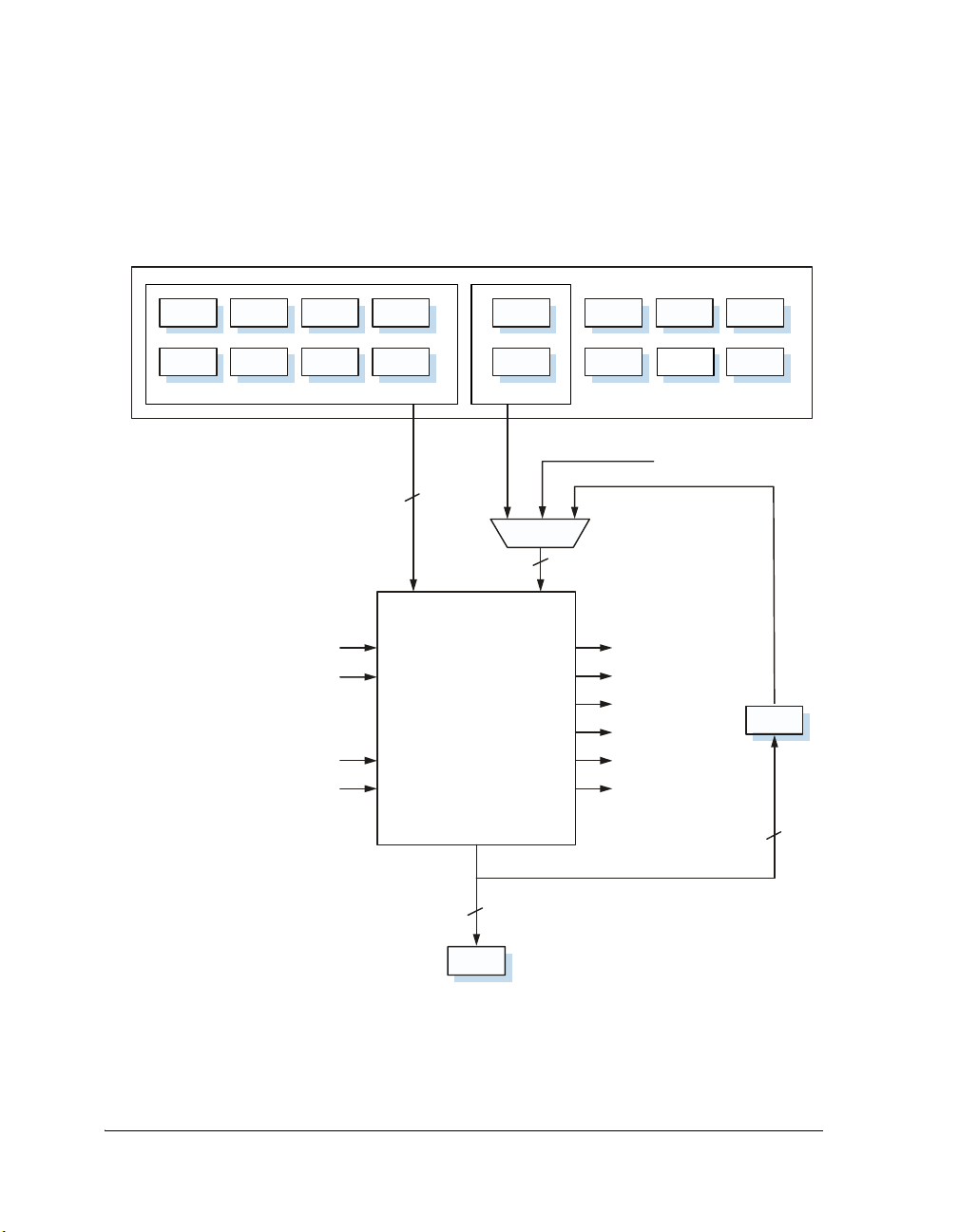
Arithmetic Logic Unit (ALU)
Preliminary
which appears in Figure 2-1 on page 2-3.
REGISTER FILE
MR2 MR1 MR0
AR AX1
AQ
AC
AR_SAT
AV_LATCH
AX0 AY0
AY1SR1 SR0
16
XY
ALU
R
MX1 MY1 SR2
16
AQ
AC
AV
AZ
AN
AS
SIMX0 MY0
CONSTANT
AF
16
16
AR
Figure 2-8. ALU Block Diagram
2-22 ADSP-2199x Mixed Signal DSP Controller Hardware Reference

Computational Units
Preliminary
The ALU is 16 bits wide with two 16-bit input ports, X and Y, and one
output port, R. The ALU accepts a carry-in signal (CI) which is the carry
bit (AC) from the processor arithmetic status register (ASTAT). The ALU
generates six status signals: the zero (AZ) status, the negative (AN) status,
the carry (AC) status, the overflow (AV) status, the X-input sign (AS) status,
and the quotient (AQ) status. All arithmetic status signals are latched into
the arithmetic status register (ASTAT) at the end of the cycle. For information on how each instruction affects the ALU flags, see Table 2-6 on
page 2-19.
Unless a NONE= instruction is executed, the output of the ALU goes into
either the ALU feedback (AF) register or the ALU result (AR) register,
which is part of the register file. The AF register is an ALU internal
register.
In unconditional and single-function instructions, both the X and the Y
port may read any register of the register file including AR. Alternatively,
the Y port may access the local feedback register AF.
For conditional and multi-function instructions only, a subset of registers
can be used as input operands. For legacy support this register usage
restriction mirrors the ADSP-218x instruction set. Then the X port can
access the register AR, SR1, SR0, MR2, MR1, MR0, AX0 and AX1. The
Y port accesses AY0, AY1 and AF.
If the X port accesses either AR, SR1, SR0, MR2, MR1, MR0, AX0 or
AX1, the Y operator may be a constant coded in the instruction word.
L
The ALU can read and write any of its associated registers in the same
cycle. Registers are read at the beginning of the cycle and written at the
end of the cycle. A register read gets the value loaded at the end of a previous cycle. A new value written to a register cannot be read out until a
subsequent cycle. This read/write pattern lets an input register provide an
ADSP-2199x Mixed Signal DSP Controller Hardware Reference 2-23
For more information on register usage restrictions in conditional
and multifunction instructions, see “Multifunction Computations”
on page 2-64.

Arithmetic Logic Unit (ALU)
Preliminary
operand to the ALU at the beginning of the cycle and be updated with the
next operand from memory at the end of the same cycle. Also, this
read/write pattern lets a result register be stored in memory and updated
with a new result in the same cycle.
Multiprecision operations are supported in the ALU with the carry-in signal and ALU carry (AC) status bit. The carry-in signal is the AC status bit
that was generated by a previous ALU operation. The “add with carry”
(+C) operation is intended for adding the upper portions of multiprecision numbers. The “subtract with borrow” (C–1 is effectively a “borrow”)
operation is intended for subtracting the upper portions of multiprecision
numbers.
ALU Division Support Features
The ALU supports division with two special divide primitives. These
instructions (Divs, Divq) let programs implement a non-restoring, conditional (error checking), add-subtract division algorithm. The division can
be either signed or unsigned, but the dividend and divisor must both be of
the same type. More details on using division and programming examples
are available in the ADSP-219x DSP Instruction Set Reference.
A single-precision divide, with a 32-bit dividend (numerator) and a 16-bit
divisor (denominator), yielding a 16-bit quotient, executes in 16 cycles.
Higher- and lower-precision quotients can also be calculated. The divisor
can be stored in AX0, AX1, or any of the R registers. The upper half of a
signed dividend can start in either AY1 or AF. The upper half of an
unsigned dividend must be in
in AY0. At the end of the divide operation, the quotient is in AY0.
The first of the two primitive instructions “divide-sign” (
at the beginning of the division when dividing signed numbers. This operation computes the sign bit of the quotient by performing an exclusive OR
of the sign bits of the divisor and the dividend. The AY0 register is shifted
one place so that the computed sign bit is moved into the LSB position.
2-24 ADSP-2199x Mixed Signal DSP Controller Hardware Reference
AF. The lower half of any dividend must be
Divs) is executed
Computational Units
5
Preliminary
The computed sign bit is also loaded into the AQ bit of the arithmetic status register. The MSB of AY0 shifts into the LSB position of AF, and the
upper 15 bits of AF are loaded with the lower 15 R bits from the ALU,
which simply passes the Y input value straight through to the R output.
The net effect is to left shift the AF-AY0 register pair and move the quotient
sign bit into the LSB position. The operation of Divs is illustrated in
Figure 2-9 on page 2-25.
1
LEFT SHI FT
AX1 AY1 AFAX0 AY0
MUX
UPPER
DIVIDEND
DIVISOR
R-BUS
MSB
X
ALU
R = PASS Y
Figure 2-9. DIVS Operation
MUX
B
S
L
16
MSB
Y
15 LSBs
LOWER
DIVIDEND
AQ
ADSP-2199x Mixed Signal DSP Controller Hardware Reference 2-25

Arithmetic Logic Unit (ALU)
Preliminary
When dividing unsigned numbers, the Divs operation is not used. Instead,
the AQ bit in the arithmetic status register (ASTAT) should be initialized to
zero by manually clearing it. The AQ bit indicates to the following operations that the quotient should be assumed positive.
The second division primitive is the “divide-quotient” (Divq) instruction,
which generates one bit of quotient at a time and is executed repeatedly to
compute the remaining quotient bits.
For unsigned single-precision divides, the Divq instruction is executed 16
times to produce 16 quotient bits. For signed single-precision divides, the
Divq instruction is executed 15 times after the sign bit is computed by the
Divs operation. Divq instruction shifts the AY0 register left by one bit so
that the new quotient bit can be moved into the LSB position.
The status of the AQ bit generated from the previous operation determines
the ALU operation to calculate the partial remainder. If AQ = 1, the ALU
adds the divisor to the partial remainder in AF. If AQ = 0, the ALU subtracts the divisor from the partial remainder in AF.
2-26 ADSP-2199x Mixed Signal DSP Controller Hardware Reference
Computational Units
5
Preliminary
The ALU output R is offset loaded into AF just as with the Divs operation.
The AQ bit is computed as the exclusive-OR of the divisor MSB and the
ALU output MSB, and the quotient bit is this value inverted. The quotient bit is loaded into the LSB of the AY0 register which is also shifted left
by one bit. The Divq operation is illustrated in Figure 2-10 on page 2-27.
1
LEFT SHIFT
B
AX0
MUX
DIVISOR
AX1
AF AY0
PARTIAL
REMAINDER
16
MSB
S
L
LOWER
DIVIDEND
R-BUS
X
ALU
R=Y+X IF AQ=1
R=Y-X IF AQ=0
Y
1MSB
15 LSBs
AQ
Figure 2-10. DIVQ Operation
ADSP-2199x Mixed Signal DSP Controller Hardware Reference 2-27

Arithmetic Logic Unit (ALU)
Preliminary
The format of the quotient for any numeric representation can be determined by the format of the dividend and divisor as shown in Figure 2-11
on page 2-28. Let NL represent the number of bits to the left of the binary
point, let NR represent the number of bits to the right of the binary point
of the dividend, let DL represent the number of bits to the left of the
binary point, and let DR represent the number of bits to the right of the
binary point of the divisor. Then, the quotient has NL–DL+1 bits to the
left of the binary point and has NR–DR–1 bits to the right of the binary
point.
Dividend BBBBB
NL bits
Divisor
Quotient
(N L – D L+ 1 ) bits
. BBBBBBBBBBBBBBBBBBBBBBBBBBB
NR bits
BB
. BBBBBBBBBBBBBB
DL bits
BBBB .
DR bits
BBBBBBBBBBBB
(NR–DR–1) bits
Figure 2-11. Quotient Format
Some format manipulation may be necessary to guarantee the validity of
the quotient. For example, if both operands are signed and fully fractional
(dividend in 1.31 format and divisor in 1.15 format) the result is fully
fractional (in 1.15 format), and the dividend must be smaller than the
divisor for a valid result.
To divide two integers (dividend in 32.0 format and divisor in 16.0 format) and produce an integer quotient (in 16.0 format), the program must
shift the dividend one bit to the left (into 31.1 format) before dividing.
Additional discussion and code examples can be found in the ADSP-219x
DSP Instruction Set Reference.
2-28 ADSP-2199x Mixed Signal DSP Controller Hardware Reference
 Loading...