


ADSP-219x/2192 DSP
Hardware Reference
Analog Devices, Inc.
One Technology Way
Norwood, Mass. 02062-9106
Revision 1.1, April 2004
Part Number
82-002001-01
a

Copyright Information
©2004 Analog Devices, Inc., ALL RIGHTS RESERVED. This document
may not be reproduced in any form without prior, express written consent
from Analog Devices, Inc.
Printed in the USA.
Disclaimer
Analog Devices, Inc. reserves the right to change this product without
prior notice. Information furnished by Analog Devices is believed to be
accurate and reliable. However, no responsibility is assumed by Analog
Devices for its use; nor for any infringement of patents or other rights of
third parties which may result from its use. No license is granted by implication or otherwise under the patent rights of Analog Devices, Inc.
Trademark and Service Mark Notice
The Analog Devices logo and VisualDSP++ are registered trademarks of
Analog Devices, Inc.
EZ-KIT Lite is a trademark of Analog Devices, Inc.
All other brand and product names are trademarks or service marks of
their respective owners.

CONTENTS
INTRODUCTION
Purpose ......................................................................................... 1-1
Audience ...................................................................................... 1-1
Overview—Why Fixed-Point DSP? ............................................... 1-2
ADSP-219x Design Advantages ..................................................... 1-2
ADSP-219x Architecture Overview ............................................... 1-5
DSP Core Architecture ............................................................ 1-7
DSP Peripherals Architecture ................................................... 1-9
Memory Architecture .............................................................. 1-9
Internal (On-Chip) Memory ............................................. 1-11
Interrupts .............................................................................. 1-12
DMA Controller ................................................................... 1-12
PCI Port ............................................................................... 1-12
USB Port .............................................................................. 1-13
AC’97 Interface ..................................................................... 1-13
Low Power Operation ............................................................ 1-13
Clock Signals ........................................................................ 1-13
Reset Modes .......................................................................... 1-14
JTAG Port ............................................................................. 1-15
ADSP-219x/2192 DSP Hardware Reference i

CONTENTS
Development Tools ..................................................................... 1-15
Differences from Previous DSPs .................................................. 1-17
Computational Units and Data Register File ..................... 1-17
Shifter Result (SR) Register as Multiplier
Dual Accumulator ......................................................... 1-18
Shifter Exponent (SE) Register is not
Memory Accessible ........................................................ 1-18
Conditions (SWCOND) and Condition Code
(CCODE) Register ........................................................ 1-19
Unified Memory Space ..................................................... 1-20
Data Memory Page (DMPG1 and DMPG2) Registers ....... 1-20
Data Address Generator (DAG) Addressing Modes ............ 1-21
Base Registers for Circular Buffers. .................................... 1-21
Program Sequencer, Instruction Pipeline, and Stacks ......... 1-22
Conditional Execution (Difference in Flag
Input Support) .............................................................. 1-22
Execution Latencies (Different for JUMP Instructions) ...... 1-23
Instruction Set Enhancements ........................................... 1-24
For More Information About Analog Products ............................. 1-24
For Technical or Customer Support ........................................... 1-25
What’s New in This Manual ....................................................... 1-25
Related Documents .................................................................... 1-25
Conventions ............................................................................... 1-27
ii ADSP-219x/2192 DSP Hardware Reference

CONTENTS
COMPUTATIONAL UNITS
Overview ...................................................................................... 2-1
Using Data Formats ...................................................................... 2-4
Binary String ........................................................................... 2-4
Unsigned ................................................................................. 2-4
Signed Numbers: Two’s Complement ....................................... 2-5
Fractional Representation: 1.15 ................................................ 2-5
ALU Data Types ...................................................................... 2-5
Multiplier Data Types .............................................................. 2-6
Shifter Data Types ................................................................... 2-7
Arithmetic Formats Summary .................................................. 2-8
Setting Computational Modes ..................................................... 2-10
Latching ALU Result Overflow Status .................................... 2-10
Saturating ALU Results on Overflow ...................................... 2-11
Using Multiplier Integer and Fractional Formats .................... 2-12
Rounding Multiplier Results .................................................. 2-14
Unbiased Rounding .......................................................... 2-14
Biased Rounding ............................................................... 2-15
Using Computational Status ........................................................ 2-16
Arithmetic Logic Unit (ALU) ...................................................... 2-17
ALU Operation ..................................................................... 2-17
ALU Status Flags ................................................................... 2-18
ALU Instruction Summary .................................................... 2-19
ADSP-219x/2192 DSP Hardware Reference iii

CONTENTS
ALU Data Flow Details ......................................................... 2-21
ALU Division Support Features ............................................. 2-23
Multiply—Accumulator (Multiplier) ........................................... 2-28
Multiplier Operation ............................................................. 2-28
Placing Multiplier Results in MR or SR Registers .............. 2-29
Clearing, Rounding, or Saturating Multiplier Results ......... 2-30
Multiplier Status Flags ........................................................... 2-31
Saturating Multiplier Results on Overflow ............................. 2-31
Multiplier Instruction Summary ............................................ 2-33
Multiplier Data Flow Details ................................................. 2-34
Barrel-Shifter (Shifter) ................................................................ 2-37
Shifter Operations ................................................................. 2-37
Derive Block Exponent ..................................................... 2-39
Immediate Shifts .............................................................. 2-40
Denormalize ..................................................................... 2-42
Normalize, Single Precision Input ..................................... 2-44
Normalize, ALU Result Overflow ...................................... 2-45
Normalize, Double Precision Input ................................... 2-47
Shifter Status Flags ................................................................ 2-50
Shifter Instruction Summary ................................................. 2-50
Shifter Data Flow Details ...................................................... 2-52
Data Register File ....................................................................... 2-57
Secondary (Alternate) Data Registers ........................................... 2-59
Multifunction Computations ...................................................... 2-60
iv ADSP-219x/2192 DSP Hardware Reference

CONTENTS
PROGRAM SEQUENCER
Overview ...................................................................................... 3-1
Instruction Pipeline ...................................................................... 3-7
Instruction Cache ......................................................................... 3-9
Using The Cache ................................................................... 3-11
Optimizing Cache Usage ....................................................... 3-12
Branches and Sequencing ............................................................ 3-14
Indirect Jump Page (IJPG) Register ........................................ 3-15
Conditional Branches ............................................................ 3-16
Delayed Branches .................................................................. 3-16
Loops and Sequencing ................................................................. 3-20
Managing Loop Stacks ........................................................... 3-24
Restrictions On Ending Loops ............................................... 3-24
Interrupts and Sequencing ........................................................... 3-24
Sensing Interrupts ................................................................. 3-30
Masking Interrupts ................................................................ 3-31
Latching Interrupts ................................................................ 3-31
Stacking Status During Interrupts .......................................... 3-32
Nesting Interrupts ................................................................. 3-32
Interrupting Idle .................................................................... 3-34
Stacks and Sequencing ................................................................ 3-34
Conditional Sequencing .............................................................. 3-39
Sequencer Instruction Summary .................................................. 3-42
ADSP-219x/2192 DSP Hardware Reference v

CONTENTS
DATA ADDRESS GENERATORS
Overview ...................................................................................... 4-1
Setting DAG Modes ..................................................................... 4-4
Secondary (Alternate) DAG Registers ...................................... 4-4
Bit-Reverse Addressing Mode .................................................. 4-6
DAG Page Registers (DMPGx) ................................................ 4-6
Using DAG Status ........................................................................ 4-8
DAG Operations .......................................................................... 4-9
Addressing with DAGs ............................................................ 4-9
Addressing Circular Buffers ................................................... 4-11
Addressing With Bit-Reversed Addresses ................................ 4-15
Modifying DAG Registers ..................................................... 4-19
DAG Register Transfer Restrictions ............................................. 4-20
DAG Instruction Summary ......................................................... 4-21
MEMORY
Overview ...................................................................................... 5-1
Internal Address and Data Buses .............................................. 5-3
Internal Data Bus Exchange .................................................... 5-5
ADSP-2192 Memory Map ............................................................ 5-8
P0 DSP Core Internal Memory Space .................................... 5-10
P1 DSP Core Internal Memory Space .................................... 5-11
Shared Memory .................................................................... 5-11
Host (PCI/USB) and DSP Internal Memory Space ................ 5-12
vi ADSP-219x/2192 DSP Hardware Reference

CONTENTS
System Control Registers ....................................................... 5-13
Shared I/O Memory-mapped Registers ................................... 5-13
Arranging Data in Memory ......................................................... 5-13
Data Move Instruction Summary ................................................. 5-14
DUAL DSP CORES
Overview ...................................................................................... 6-1
Shared Dual DSP Core Settings ............................................... 6-1
Unique DSP Core Settings ....................................................... 6-2
Setting Dual DSP Core Features .................................................... 6-3
System Control ....................................................................... 6-3
Power Down Mode Control ..................................................... 6-5
Clock Multiplier Mode Control ............................................. 6-10
GPIO and Serial EEPROM Mode Control ............................. 6-11
Using Dual-DSP Interrupts and Flags .......................................... 6-13
Controlling I/O Register Bus Accesses ......................................... 6-17
Using DSP and PCI Mailbox Registers ........................................ 6-20
Mailbox Status (MBXSTAT) Register ................................ 6-21
Mailbox Interrupt Control (MBXCTL) Register ................ 6-24
InBox 0 - PCI/USB to DSP Mailbox 0
(MBX_IN0) Register ...................................................... 6-26
InBox 1 - PCI/USB to DSP Mailbox 1
(MBX_IN1) Register ...................................................... 6-26
ADSP-219x/2192 DSP Hardware Reference vii

CONTENTS
OutBox 0 - DSP to PCI/USB Mailbox 0
(MBX_OUT0) Register ................................................. 6-26
OutBox 1 - DSP to PCI/USB Mailbox 1
(MBX_OUT1) Register ................................................. 6-26
I/O PROCESSOR
Overview ...................................................................................... 7-1
Setting I/O Processor—Host Port Modes .................................... 7-12
Host Port Buffer Modes ........................................................ 7-14
Host Port Scatter-Gather DMA Mode ................................... 7-16
Setting I/O Processor—AC’97 Port Modes .................................. 7-18
Host Port DMA Status ............................................................... 7-19
DMA Controller Operation ........................................................ 7-20
Managing DMA Channel Priority ......................................... 7-21
Chaining DMA Processes ...................................................... 7-22
Host Port DMA .......................................................................... 7-22
AC’97 Port DMA ....................................................................... 7-24
HOST (PCI/USB) PORT
Overview ...................................................................................... 8-1
Host Port Selection ................................................................. 8-1
Mode Strap Pin Connections ................................................... 8-2
PCI Parallel Interface .................................................................... 8-2
Configuration Spaces .............................................................. 8-2
Interactions Between Functions ........................................... 8-5
Base Address Registers ........................................................ 8-8
Peripheral Device Control Registers .................................... 8-9
viii ADSP-219x/2192 DSP Hardware Reference

CONTENTS
Power Management Interactions .............................................. 8-9
PCI Clock Domain ............................................................... 8-11
Peripheral Device Control Register Access .............................. 8-12
Resets .................................................................................... 8-14
Interrupts .............................................................................. 8-14
PCI Control Register ............................................................. 8-16
PCI Port Priority on the PDC Bus ..................................... 8-18
DSP Mailbox Registers .......................................................... 8-18
InBoxes ............................................................................ 8-18
OutBoxes .......................................................................... 8-19
Status ............................................................................... 8-19
Control ............................................................................. 8-21
Indirect Access to I/O Space .................................................. 8-23
USB Interface ............................................................................. 8-25
Overview .............................................................................. 8-25
USB Requirements ................................................................ 8-25
Implementation ..................................................................... 8-26
Block Diagram of USB Module ............................................. 8-27
USB-SIE ........................................................................... 8-27
Endpoint 0 Control .......................................................... 8-28
MCU ............................................................................... 8-28
I/O REG Interface ............................................................ 8-29
DSP DMA Interface ......................................................... 8-29
DSP Code/Data Endpoint Control .................................... 8-29
ADSP-219x/2192 DSP Hardware Reference ix

CONTENTS
Features and Modes ............................................................... 8-30
Endpoint Types ................................................................ 8-30
Data Transfers .................................................................. 8-30
References ............................................................................. 8-32
MCU Register Definitions .................................................... 8-33
Config USB Device Definitions and
Descriptor Tables ............................................................... 8-52
Vendor-Specific Commands .................................................. 8-55
DSP Register Definitions ...................................................... 8-58
USB DSP Register Definitions .............................................. 8-58
DSP Code Download ............................................................ 8-65
General Comments ........................................................... 8-67
Starting DSP Code Execution ........................................... 8-67
MCU ROM Firmware Structure ....................................... 8-70
MCU Firmware Programmers Model (Endpoint 0) ............ 8-72
Example Initialization Process ............................................... 8-81
Config Device Definition ................................................. 8-85
Modem Device Definition ................................................ 8-85
Serial EEPROM Interface ................................................. 8-86
Serial EEPROM Changeable Fields for USB Descriptors ... 8-86
ADSP-2192 USB Data Pipe Operations ................................ 8-87
OUT Transactions (Host to Device) .................................. 8-91
IN Transactions (Device to Host) ..................................... 8-92
Register and Bit #Defines File ..................................................... 8-94
x ADSP-219x/2192 DSP Hardware Reference

CONTENTS
AC’97 CODEC PORT
Overview ...................................................................................... 9-1
ADSP-2192 Features and Functionality ......................................... 9-1
FIFO Control and Status Register ................................................. 9-3
FIFO Transmit Control and Status Register ............................. 9-3
FIFO Receive Control and Status Register ................................ 9-5
FIFO DMA Address Registers .................................................. 9-8
FIFO DMA Current Count Registers ....................................... 9-8
FIFO DMA Count Registers .................................................... 9-9
FIFO DMA Next Address Registers ......................................... 9-9
16-bit Transmit Data Register ............................................. 9-9
16-bit Receive Data Register ................................................ 9-9
AC-Link Digital Serial Interface Protocol ............................... 9-10
Resetting the AC’97 .......................................................... 9-12
ADSP-2192 AC’97 Control Registers .......................................... 9-13
AC’97 Link Control/Status Register (AC97LCTL) ................. 9-15
AC’97 Link Status Register (AC97STAT) ............................... 9-19
AC’97 Slot Enable Register (AC97SEN) ................................ 9-21
AC’97 Input Slot Valid Register (AC97SVAL) ........................ 9-22
AC’97 AC97STAT:REG and Frame Interrupt Timing ........ 9-22
AC’97 External Codec Register Spaces ............................... 9-23
AC’97 Slot Request Register (AC97SREQ) ............................ 9-24
AC’97 GPIO Status Register (AC97SIF) ................................ 9-24
ADSP-219x/2192 DSP Hardware Reference xi

CONTENTS
ADSP-2192 AC’97 Audio Interface ............................................. 9-25
External Audio Codec (AC’97) Subsystem ............................. 9-25
Resource Allocation .......................................................... 9-25
AC’97 2.1 Protocol Summary ..................................................... 9-27
Access to AC’97 Codec Control/Status Registers .................... 9-28
AC’97 2.1 Link Powerdown States ......................................... 9-30
State Transitions ............................................................... 9-33
Configuring AC’97 Sample Data Streams .................................... 9-36
JTAG TEST-EMULATION PORT
SYSTEM DESIGN
Overview .................................................................................... 11-1
Sources for Additional Information ............................................. 11-1
Pin Descriptions ......................................................................... 11-3
Clock Signals .............................................................................. 11-7
Synchronization Delay .......................................................... 11-9
Configurable Clock Multiplier Considerations .................... 11-10
Maximizing Performance of DSP Algorithms ............................. 11-11
Resetting the Processor ............................................................. 11-13
Power On Reset .................................................................. 11-13
Forced Reset Via PCI/USB .................................................. 11-14
Software Reset .................................................................... 11-14
Reset Progression ................................................................ 11-14
Resets and Software-Forced Rebooting ................................. 11-16
xii ADSP-219x/2192 DSP Hardware Reference

CONTENTS
Interrupts ................................................................................. 11-22
Flag Pins ................................................................................... 11-22
Powerup and Powerdown .......................................................... 11-23
Powerup Issues .......................................................................... 11-24
Powerup Sequence ............................................................... 11-24
Power Regulators ................................................................. 11-26
2.5V Regulator Options .................................................. 11-27
Power Management Description .......................................... 11-28
Powerdown ............................................................................... 11-29
Powerdown Control ............................................................. 11-30
Entering and Exiting Powerdown ......................................... 11-31
Powering Down the USB ..................................................... 11-32
Powering Down the PCI ...................................................... 11-32
Powering Down the AC’97 Link .......................................... 11-33
Entering Powerdown ........................................................... 11-34
Exiting Powerdown .............................................................. 11-35
Ending Powerdown ......................................................... 11-35
Ending Powerdown with the PORST Pin ......................... 11-35
Startup Time after Powerdown ............................................. 11-36
Using an External TTL/CMOS Clock ............................. 11-36
Processor Operation During Powerdown .............................. 11-36
Interrupts And Flags ....................................................... 11-37
Conditions for Lowest Power Consumption ......................... 11-37
AC’97 Low Power Mode ................................................ 11-38
Using Powerdown as A Non-Maskable Interrupt ................... 11-39
ADSP-219x/2192 DSP Hardware Reference xiii

CONTENTS
Emulation ................................................................................ 11-39
EZ-KIT Lite ............................................................................. 11-40
Recommended Reading ............................................................ 11-41
ADSP-219X DSP CORE REGISTERS
Overview ...................................................................................... A-1
Core Registers Summary ......................................................... A-2
Register Load Latencies ........................................................... A-5
Core Status Registers .................................................................... A-8
Arithmetic Status (ASTAT) Register ........................................ A-9
Mode Status (MSTAT) Register ............................................. A-11
System Status (SSTAT) Register ............................................. A-14
Computational Unit Registers ..................................................... A-15
Data Register File (DREG) Registers ..................................... A-16
ALU X- and Y-Input (AX0, AX1, AY0, AY1) Registers ........... A-16
ALU Results (AR) Register .................................................... A-17
Multiplier X- and Y-Input (MX0, MX1, MY0, MY1)
Registers ............................................................................ A-17
Multiplier Results (MR2, MR1, MR0) Registers .................... A-17
Shifter Input (SI) Register ..................................................... A-17
Shifter Exponent (SE) and Block Exponent (SB) Registers ...... A-18
Program Sequencer Registers ....................................................... A-18
Interrupt Mask (IMASK) and Interrupt
Latch (IRPTL) Registers ..................................................... A-19
Interrupt Control (ICNTL) Register ...................................... A-20
xiv ADSP-219x/2192 DSP Hardware Reference

CONTENTS
Indirect Jump Page (IJPG) Register ....................................... A-21
PC Stack Page (STACKP) and
PC Stack Address (STACKA) Registers ............................... A-21
Loop Stack Page (LPSTACKP) and
Loop Stack Address (LPSTACKA) Register ......................... A-22
Counter (CNTR) Register .................................................... A-22
Condition Code (CCODE) Register ..................................... A-23
Cache Control (CACTL) Register ......................................... A-23
Data Address Generator Registers ............................................... A-24
Index Registers (Ix) ............................................................... A-24
Modify Registers (Mx) .......................................................... A-24
Length and Base (Lx,Bx) Registers ........................................ A-25
Data Memory Page (DMPGx) Register ................................. A-25
Memory Interface Registers ........................................................ A-26
PM Bus Exchange (PX) Register ........................................... A-26
I/O Memory Page (IOPG) Register ....................................... A-26
Register and Bit #Defines File .................................................... A-27
ADSP-2192 DSP PERIPHERAL REGISTERS
Overview ..................................................................................... B-1
Peripheral Registers ...................................................................... B-2
DSP Peripherals Architecture .................................................. B-3
Peripheral Device Register Groups ................................................ B-4
Summary ............................................................................... B-4
ADSP-219x/2192 DSP Hardware Reference xv

CONTENTS
ADSP-2192 System Control Registers ........................................... B-6
STCTLx FIFO Transmit Control Register ........................... B-9
SRCTLx FIFO Receive Control Register ............................. B-9
xxxADDR DMA Address Register ..................................... B-10
xxxNXTADDR DMA Next Address Register ..................... B-10
xxxCNT DMA Count Register ......................................... B-10
xxxCURCNT DMA Current Count Register ..................... B-10
ADSP-2192 Peripheral Device Control Registers ......................... B-11
ADSP-2192 Chip Control Registers ...................................... B-13
Chip Control (SYSCON) Registers ................................... B-14
Power Management Functions .......................................... B-18
DSP Powerdown (PWRPx) Registers ................................. B-19
DSP PLL Control (PLLCTL) Register ............................... B-23
General-purpose I/O (GPIO) Control Registers ..................... B-24
GPIO Configuration (GPIOCFG) Register ....................... B-25
GPIO Polarity (GPIOPOL) Register ................................. B-25
GPIO Sticky (GPIOSTKY) Register .................................. B-26
GPIO Wakeup Control (GPIOWAKECTL) Register ......... B-26
GPIO Status (GPIOSTAT) Register .................................. B-26
GPIO Control (GPIOCTL) Register ................................. B-27
GPIO Pullup (GPIOPUP) Register ................................... B-27
GPIO Pulldown (GPIOPDN) Register .............................. B-27
EEPROM I/O Control/Status (SPROMCTL) Register ........... B-28
xvi ADSP-219x/2192 DSP Hardware Reference

CONTENTS
Host Mailbox Registers ......................................................... B-30
Overview ......................................................................... B-30
CardBus Function Event Registers ........................................ B-32
CSTSCHG Signal ............................................................ B-33
INTA Signal .................................................................... B-34
CIS Tuple Requirements .................................................. B-35
AC’97 Controller Registers ................................................... B-41
AC’97 Link Control/Status Register (AC97LCTL) ............ B-42
AC’97 Link Status Register (AC97STAT) ......................... B-42
AC’97 Slot Enable Register (AC97SEN) ........................... B-43
AC’97 Input Slot Valid Register (AC97SVAL) .................. B-43
AC’97 Slot Request Register (AC97SREQ) ....................... B-44
AC’97 GPIO Status Register (AC97SIF) ........................... B-44
AC’97 Codec Registers ........................................................ B-45
AC’97 Codec Register Space-Primary Codec 0
(AC97EXT0) Register .................................................. B-45
AC’97 Codec Register Space, Secondary Codec 1
(AC97EXT1) Register .................................................. B-45
AC’97 Codec Register Space, Secondary Codec 2
(AC97EXT2) Register .................................................. B-46
PCI DMA Address, Count Registers ..................................... B-46
DMA Control Registers ................................................... B-46
PCI DMA Control Registers ............................................ B-46
PCI Interrupt, Control Registers ........................................... B-47
ADSP-219x/2192 DSP Hardware Reference xvii

CONTENTS
DMA Transfer Count 0 - Bus Master Sample Transfer
Count (PCI_MSTRCNT0) Register ............................... B-48
DMA Transfer Count 1 - Bus Master Sample Transfer
Count (PCI_MSTRCNT1) Register ............................... B-48
DMA Control X - Bus Master Control and Status
(PCI_DMACx) Register ................................................. B-49
PCI Interrupt (PCI_IRQSTAT) Register ........................... B-50
PCI Control (PCI_CFGCTL) Register .............................. B-53
PCI Configuration Register Space ......................................... B-54
Commonalities Between the Three Functions .................... B-54
Interactions Between the Three Functions ......................... B-55
PCI Configuration Register Space, Function 0 .................. B-56
PCI Configuration Register Space, Function 1 .................. B-58
PCI Configuration Register Space, Function 2 .................. B-59
PCI Configuration Space .................................................. B-60
Interaction Between Registers ........................................... B-67
USB DSP Registers ............................................................... B-71
Overview .......................................................................... B-71
DSP Register Definitions ...................................................... B-72
DSP Memory Buffer Base Addr Register ................................ B-74
DSP Memory Buffer Size Register .................................... B-75
DSP Memory Buffer RD Pointer Offset Register .................... B-75
DSP Memory Buffer WR Pointer Offset Register .................. B-76
MCU Register Definitions .................................................... B-76
USB Endpoint Description Register ...................................... B-79
xviii ADSP-219x/2192 DSP Hardware Reference

CONTENTS
USB Endpoint NAK Counter Register .................................. B-80
USB Endpoint Stall Policy Register ....................................... B-81
USB Endpoint 1 Code Download Base Address Register ........ B-82
USB Endpoint 2 Code Download Base Address Register ........ B-83
USB Endpoint 3 Code Download Base Address Register ........ B-84
USB Endpoint 1 Code Download Current Write
Pointer Offset Register ....................................................... B-85
USB Endpoint 2 Code Download Current Write
Pointer Offset Register ...................................................... B-86
USB Endpoint 3 Code Download Current Write
Pointer Offset Register ...................................................... B-87
USB SETUP Token Command Register ................................ B-88
USB SETUP Token Data Register ......................................... B-89
USB SETUP Counter Register .............................................. B-90
USB Register I/O Address Register ....................................... B-91
USB Register I/O Data Register ........................................... B-92
USB Control Register ........................................................... B-93
USB Address/Endpoint Register ............................................ B-94
USB Frame Number Register ................................................ B-94
Register and Bit #Defines File .................................................... B-95
ADSP-219x/2192 DSP Hardware Reference xix

CONTENTS
NUMERIC FORMATS
Overview ...................................................................................... C-1
Un/Signed: Twos-Complement Format ......................................... C-1
Integer or Fractional ..................................................................... C-1
Binary Multiplication ................................................................... C-5
Fractional Mode And Integer Mode ......................................... C-6
Block Floating-Point Format ......................................................... C-7
ADSP-2192 TIMER
Overview ..................................................................................... D-1
Timer Architecture ...................................................................... D-2
Resolution ................................................................................... D-4
Timer Operation ......................................................................... D-4
Enabling the Timer ...................................................................... D-6
ADSP-2192 INTERRUPTS
Overview ...................................................................................... E-1
Peripheral Interrupts ..................................................................... E-1
Other Interrupt Types ................................................................... E-4
GLOSSARY
Terms .......................................................................................... G-1
INDEX
xx ADSP-219x/2192 DSP Hardware Reference

1 INTRODUCTION
Figure 1-0.
Table 1-0.
Listing 1-0.
Purpose
The ADSP-219x/2192 DSP Hardware Reference provides architectural
information on the ADSP-219x modified Harvard architecture Digital
Signal Processor (DSP) core and ADSP-2192 DSP product. The architectural descriptions cover functional blocks, buses, and ports, including all
features and processes they support. For programming information, see
the ADSP-219x DSP Instruction Set Reference.
Audience
DSP system designers and programmers who are familiar with signal processing concepts are the primary audience for this manual. This manual
assumes that the audience has a working knowledge of microcomputer
technology and DSP-related mathematics.
DSP system designers and programmers who are unfamiliar with signal
processing can use this manual, but they should supplement this manual
with other texts that describe DSP techniques.
All readers, particularly system designers, should refer to the DSP’s data
sheet for timing, electrical, and package specifications. For additional suggested reading, see “For More Information About Analog Products” on
page 1-24.
ADSP-219x/2192 DSP Hardware Reference 1-1

Overview—Why Fixed-Point DSP?
Overview—Why Fixed-Point DSP?
A digital signal processor’s data format determines its ability to handle signals of differing precision, dynamic range, and signal-to-noise ratios.
Because 16-bit, fixed-point DSP math is required for certain DSP coding
algorithms, using a 16-bit, fixed-point DSP can provide all the features
needed for certain algorithm and software development efforts. Also, a
narrower bus width (16-bit as opposed to 32- or 64-bit wide) leads to
reduced power consumption and other design savings. The extent to
which this is true depends on the fixed-point processor’s architecture.
High-level language programmability, large address spaces, and wide
dynamic range allow system development time to be spent on algorithms
and signal processing concerns, rather than assembly language coding,
code paging, and error handling. The ADSP-2192 DSP is a highly integrated, 16-bit fixed-point DSP that provides many of these design
advantages.
ADSP-219x Design Advantages
The ADSP-219x family DSPs are high-performance 16-bit DSPs for communications, instrumentation, industrial/control, voice/speech, medical,
military, and other applications. These DSPs provide a DSP core that is
compatible with previous ADSP-2100 family DSPs, but they also provide
many additional features. The ADSP-219x core combines with on-chip
peripherals to form a complete system-on-a-chip. The off-core peripherals
add on-chip SRAM, integrated I/O peripherals, timer, and interrupt
controller.
The ADSP-219x architecture balances a high performance processor core
with high performance buses (PM, DM, DMA). In the core, every computational instruction can execute in a single cycle. The buses and
instruction cache provide rapid, unimpeded data flow to the core to maintain the execution rate.
1-2 ADSP-219x/2192 DSP Hardware Reference
Introduction
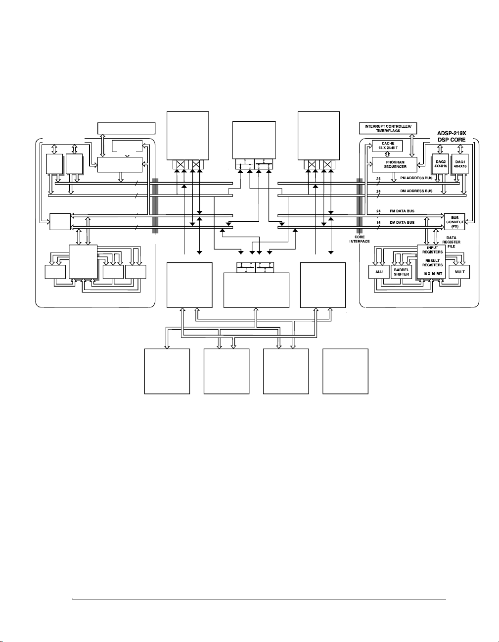
Figure 1-1 shows a detailed block diagram of the ADSP-2192 processor.
P1
MEMORY
ⴛ24 PM
16K
ⴛ16 DM
32K
BOOT ROM
ADDR DATAADDR DATA
P1 DMA
CONTROLLER
FIFOS
ADSP-21 9X
DSP CORE
DAG2
DAG1
4X4X 16
4X4X16
BUS
CONNEC
T
(PX)
DATA
REGISTER
FILE
MULT
PM ADDRESS BUS
DM ADDRESS BUS
INPUT
REGISTERS
RESULT
REGISTERS
16 X 16-BIT
INTERRUPT CONTROLLER/
TIMER/FLA GS
CACHE
64 X 24-
BIT
PROGRAM
SEQUENCER
2
4
2
4
PM DATA BUS
DM DATA BUS
BARREL
SHIFTER
2
4
1
6
ALU
P0
MEMORY
16K
ⴛ24 PM
64K
ⴛ16 DM
BOOT ROM
ADDR DATA ADDR DATA
CORE
INTERFACE
P0 DMA
CONTROLLER
FIFOS
SHARED
MEMORY
4K
ⴛ16 DM
ADDR DATA
ADDR DATA
SHARED DSP
I/O MA P P E D
REGISTERS
PROCESSOR P 0 PROCESSOR P1
GP I/O PINS
(& OPTIONAL
SERIAL
EEPROM)
SERIAL PORT
AC'97
COMPLIANT
HOST PORT
PCI 2.2
OR
USB 1.1
JTAG
EMULATION
PORT
Figure 1-1. ADSP-2192 Block Diagram
This diagram illustrates the following ADSP-2192 architectural features:
• Computation units for the ADSP-219x family—multiplier, ALU,
shifter, and data register file
• Program sequencer for the ADSP-219x family, with related instruction cache, interval timer, and Data Address Generators (DAG1 and
DAG2)
• PCI/USB Host port
ADSP-219x/2192 DSP Hardware Reference 1-3

ADSP-219x Design Advantages
• AC’97 codec port
• SRAM for the ADSP-2192
• Input/Output (I/O) processor with integrated DMA controllers
• JTAG Test Access Port for board test and emulation on the
ADSP-2192
Figure 1-1 also shows the two cores of the ADSP-2192 (processors P0 and
P1). Additionally, it shows the four on-chip buses of the ADSP-2192: the
Program Memory Address (PMA) bus, Program Memory Data (PMD)
bus, Data Memory Address (DMA) bus, and the Data Memory Data
(DMD) bus. During a single cycle, these buses let the processor access two
data operands (one from PMD and one from DMD), and access an
instruction (from the cache).
Further, the ADSP-219x addresses the five central requirements for DSPs:
• Fast, flexible arithmetic computation units
• Unconstrained data flow to and from the computation units
• Extended precision and dynamic range in the computation units
• Dual address generators with circular buffering support
• Efficient program sequencing
Unconstrained Data Flow. The ADSP-219x has a modified Harvard
architecture combined with a data register file. In every cycle, the DSP
can:
• Read two values from memory or write one value to memory
• Complete one computation
• Write up to three values back to the register file
1-4 ADSP-219x/2192 DSP Hardware Reference

Introduction
Fast, Flexible Arithmetic. The ADSP-219x family DSPs execute all computational instructions in a single cycle. They provide both fast cycle
times and a complete set of arithmetic operations.
40-Bit Extended Precision. The DSP handles 16-bit integer and fractional
formats (twos-complement and unsigned). The processors carry extended
precision through result registers in their computation units, limiting
intermediate data truncation errors.
Dual Address Generators. The DSP has two data address generators
(DAGs) that provide immediate or indirect (pre- and post-modify)
addressing. Modulus and bit-reverse operations are supported with only
memory page constraints on data buffer placement.
Efficient Program Sequencing. In addition to zero-overhead loops, the
DSP supports quick setup and exit for loops. Loops are both nestable
(eight levels in hardware) and interruptable. The processors support both
delayed and non-delayed branches.
ADSP-219x Architecture Overview
An ADSP-219x is a single-chip microcomputer optimized for digital signal processing (DSP) and other high speed numeric processing
applications. These DSPs provide a complete system-on-a-chip, integrating a large, high-speed SRAM and I/O peripherals supported by a
dedicated I/O bus. The following sections summarize the features of each
functional block in the ADSP-219x architecture, which appears in
Figure 1-1 on page 1-3.
The ADSP-2192 combines the ADSP-219x family base architecture (three
computational units, two data address generators, and a program
sequencer) with PCI/USB interface, AC’97 serial port, a programmable
timer, a DMA controller, general-purpose Programmable Flag pins, extensive interrupt capabilities, and on-chip program and data memory blocks.
ADSP-219x/2192 DSP Hardware Reference 1-5

ADSP-219x Architecture Overview
The ADSP-2192 architecture is code compatible with ADSP-218x family
DSPs. Though the architectures are compatible, the ADSP-2192 architecture has a number of enhancements over the ADSP-218x architecture.
The enhancements to computational units, data address generators, and
program sequencer make the ADSP-2192 more flexible and even easier to
program than the ADSP-218x DSPs.
Indirect addressing options provide addressing flexibility—pre-modify
with no update, pre- and post-modify by an immediate 8-bit, two’s-complement value and base address registers for easier implementation of
circular buffering.
The ADSP-2192 integrates 128K words of on-chip memory configured as
32K words (24-bit) of program RAM (16K words each on DSP P0 and
DSP P1) and 96K words (16-bit) of data RAM (64K words on DSP P0
and 32K words on DSP P1). Power-down circuitry is also provided to
meet the low power needs of battery operated portable equipment.
The ADSP-2192’s flexible architecture and comprehensive instruction set
support multiple operations in parallel. For example, in one processor
cycle, each core of the ADSP-2192 can:
• Generate an address for the next instruction fetch
• Fetch the next instruction
• Perform one or two data moves
• Update one or two data address pointers
• Perform a computational operation
1-6 ADSP-219x/2192 DSP Hardware Reference

Introduction
DSP Core Architecture
The ADSP-219x instruction set provides flexible data moves and multifunction (one or two data moves with a computation) instructions. Every
single-word instruction can be executed in a single processor cycle. The
ADSP-219x assembly language uses an algebraic syntax for ease of coding
and readability. A comprehensive set of development tools supports program development.
Figure 1-1 on page 1-3 shows the architecture of the ADSP-219x core. It
contains three independent computational units: the ALU, the multiplier/accumulator, and the shifter.
The computational units process 16-bit data from the register file and
have provisions to support multiprecision computations. The ALU performs a standard set of arithmetic and logic operations; division primitives
also are supported. The multiplier performs single-cycle multiply, multiply/add, and multiply/subtract operations. The multiplier now has two
40-bit accumulator results. The shifter performs logical and arithmetic
shifts, normalization, denormalization, and derive exponent operations.
The shifter can efficiently implement numeric format control, including
multiword and block floating-point representations.
Register-usage rules influence placement of input and results within the
computational units. For all unconditional, non-multi-function instructions, the computational units’ data registers act as a data register file,
permitting any input or result register to provide input to any unit for a
computation. For feedback operations, the computational units let the
output (result) of any unit be input to any unit on the next cycle. For conditional or multifunction instructions, there are restrictions limiting
which data registers may provide inputs or receive results from each computational unit. For more information, see “Multifunction
Computations” on page 2-60.
ADSP-219x/2192 DSP Hardware Reference 1-7

ADSP-219x Architecture Overview
A powerful program sequencer controls the flow of instruction execution.
The sequencer supports conditional jumps, subroutine calls, and low
interrupt overhead. With internal loop counters and loop stacks, the
ADSP-2192 executes looped code with zero overhead; no explicit jump
instructions are required to maintain loops.
Two data address generators (DAGs) provide addresses for simultaneous
dual operand fetches (from data memory and program memory). Each
DAG maintains and updates four 16-bit address pointers. Whenever the
pointer is used to access data (indirect addressing), it is pre- or post-modified by the value of one of four possible modify registers. A length value
and base address may be associated with each pointer to implement automatic modulo addressing for circular buffers.
Page registers in the DAGs allow circular addressing within 64K word
boundaries of each of the 256 memory pages, but these buffers may not
cross page boundaries. Secondary registers duplicate all the primary registers in the DAGs; switching between primary and secondary registers
provides a fast context switch.
Efficient data transfer in the core is achieved by using internal buses:
• Program Memory Address (PMA) Bus
• Program Memory Data (PMD) Bus
• Data Memory Address (DMA) Bus
• Data Memory Data (DMD) Bus
• IO or DMA Address Bus
• IO or DMA Data Bus
1-8 ADSP-219x/2192 DSP Hardware Reference

Introduction
Program memory can store both instructions and data, permitting the
ADSP-219x to fetch two operands in a single cycle, one from program
memory and one from data memory. The DSP’s dual memory buses also
let the ADSP-219x core fetch an operand from data memory and the next
instruction from program memory in a single cycle.
DSP Peripherals Architecture
Figure 1-1 on page 1-3 shows the DSP’s on-chip peripherals, as part of a
typical ADSP-2192 system with peripheral connections.The ADSP-2192
has a 16-bit PCI/USB host port. This port provides either PCI or USB
functionality via the Peripheral Device Control (PDC) bus.
The ADSP-2192 can respond to up to thirteen interrupts, using a priority
scheme implemented by the interrupt controller.
Memory Architecture
The ADSP-2192 integrates 128K words of on-chip memory configured as
32K words (24-bit) of program RAM (16K words each on DSP P0 and
DSP P1) and 96K words (16-bit) of data RAM (64K words on DSP P0
and 32K words on DSP P1). Power-down circuitry is also provided to
meet the low power needs of battery operated portable equipment.
For more information on these blocks, see the section “ADSP-2192 Mem-
ory Map” on page 5-8, which discusses the memory map in detail.
Figure 1-2 shows the ADSP-2192’s memory map.
ADSP-219x/2192 DSP Hardware Reference 1-9

ADSP-219x Architecture Overview
DSP P0
PAGE 2
PAGE 1
PAGE 0
MEMORY MAP
SHARED RAM
(16x4K)
RESERVED
PROGRAM ROM,
24x4K
PROGRAM RAM,
(24x16K)
DATA RAM
BLOCK3
(16x16K)
DATA RAM
BLOCK2
(16x16K)
DATA RAM
BLOCK1
(16x16K)
DATA RAM
BLOCK0
(16x16K)
ADDRESS
0x02 0FFF
0x02 0000
0x01 FFFF
0x01 5000
0x01 4FFF
0x01 4000
0x01 3FFF
0x01 0000
0x00 FFFF
0x00 C000
0x00 BFFF
0x00 8000
0x00 7FFF
0x00 4000
0x00 3FFF
0x00 0000
Figure 1-2. ADSP-2192 Memory Maps
SAME
SHARED
DSP I/O
MAPPED
REGISTERS
PAGES 0-255
(16x256)
ADDRESS
0xFF FF
0x00 00
PAGE 2
PAGE 1
PAGE 0
DSP P1
MEMORY MA P
SHARED RAM
(16x4K)
RESERVED
PROGRAM ROM,
24x4K
PROGRAM RAM,
(24x16K)
RESERVED
DATA RAM
BLOCK1
(16x16K)
DATA RAM
BLOCK0
(16x16K)
ADDRESS
0x02 0FFF
0x02 0000
0x01 FFFF
0x01 5000
0x01 4FFF
0x01 4000
0x01 3FFF
0x01 0000
0x00 FFFF
0x00 8000
0x00 7FFF
0x00 4000
0x00 3FFF
0x00 0000
1-10 ADSP-219x/2192 DSP Hardware Reference

Introduction
Internal (On-Chip) Memory
The ADSP-2192’s unified program and data memory space consists of
16M locations that are accessible through two 24-bit address buses, the
PMA and DMA buses. The DSP uses slightly different mechanisms to
generate a 24-bit address for each bus. The DSP has three functions that
support access to the full memory map:
• The DAGs generate 24-bit addresses for data fetches from the entire
DSP memory address range. Because DAG index (address) registers
are 16 bits wide and hold the lower 16-bits of the address, each of
the DAGs has its own 8-bit page register (DMPGx) to hold the most
significant eight address bits. Before a DAG generates an address,
the program must set the DAG’s DMPGx register to the appropriate
memory page.
• The Program Sequencer generates the addresses for instruction
fetches. For relative addressing instructions, the program sequencer
bases addresses for relative jumps, calls, and loops on the 24-bit Program Counter (PC). For direct addressing instructions (two-word
instructions), the instruction provides an immediate 24-bit address
value. The PC allows linear addressing of the full 24 bit address
range.
• The Program Sequencer relies on an 8-bit Indirect Jump page (IJPG)
register to supply the most significant eight address bits for indirect
jumps and calls that use a 16-bit DAG address register for part of
the branch address. Before a cross page jump or call, the program
must set the program sequencer’s
IJPG register to the appropriate
memory page.
ADSP-219x/2192 DSP Hardware Reference 1-11

ADSP-219x Architecture Overview
The ADSP-2192 has 4K words of on-chip ROM that holds boot routines.
If peripheral booting is selected, the DSP starts executing instructions
from the on-chip boot ROM, which starts the boot process from the
selected peripheral. For more information, see “Reset Modes” on page
1-14. The on-chip boot ROM is located on Page 255 in the DSP’s mem-
ory map.
Interrupts
The interrupt controller lets the DSP respond to thirteen interrupts with
minimum overhead.
DMA Controller
The ADSP-2192 has a DMA controller that supports automated data
transfers with minimal overhead for the DSP core. Cycle stealing DMA
transfers can occur between the ADSP-2192’s internal memory and any of
its DMA capable peripherals. Additionally, DMA transfers also can be
accomplished between any of the DMA capable peripherals. DMA capable
peripherals include the PCI, USB, and AC’97. Each individual DMA
capable peripheral has one or more dedicated DMA channels. DMA
sequences do not contend for bus access with the DSP core, instead DMAs
“steal” cycles to access memory.
PCI Port
The ADSP-2192 can interface with a host computer through a PCI port.
The PCI port accesses the DSPs via the Peripheral Device Control (PDC)
bus. The PCI port connects through the internal PCI interface to the
PDC bus.
1-12 ADSP-219x/2192 DSP Hardware Reference

Introduction
USB Port
The ADSP-2192 can interface with a host computer through a USB port.
The USB port accesses the DSPs via the Peripheral Device Control (PDC)
bus. The USB port connects through the internal USB interface to the
PDC bus.
AC’97 Interface
The ADSP-2192 includes an AC’97 interface that complies with the
AC’97 specification. The AC’97 interface connects the host’s Digital Controller (DC) chip set and between one and four analog codecs.
Low Power Operation
All pins on the ADSP-2192 remain active as long as power is maintained
to the chip. This chip does not have a specifically-defined powerdown
state; at any time either or both of the two processors can be in a low
power state, and any or all of the interfaces can be in a low power state.
Additionally, each peripheral interface (USB, PCI, and AC’97) can be put
into a low power mode, as described in “System Design” on page 11-1.
Clock Signals
The ADSP-2192 can be clocked by a crystal oscillator. If a crystal oscillator is used, the crystal should be connected across the
two capacitors connected as shown in Figure 1-3 on page 1-14. Capacitor
values are dependent on crystal type and should be specified by the crystal
manufacturer. A parallel-resonant, fundamental frequency, microprocessor-grade 24.576 MHz crystal should be used for this configuration.
ADSP-219x/2192 DSP Hardware Reference 1-13
XTALI/O pins, with

ADSP-219x Architecture Overview
24.576 MHz
XTALI XTALO
ADSP-2192
BUS SELECT
POWER ON RESET
(NO C O N NE CT )
PCI CLOCK RUN
PCI CLOCK
PCI RESET
AC'97 BIT CLOCK
CLKSEL
BUS1
BUS0
PORST
CLKRUN
CLK
RST
BITCLK
Figure 1-3. ADSP-2192 External Crystal Connections
Reset Modes
The ADSP-2192 can be reset in three ways: Power On Reset, Software
Reset, or Forced Reset Via PCI or USB.
See “Resetting the Processor” on page 11-13 for more details about
booting.
1-14 ADSP-219x/2192 DSP Hardware Reference

Introduction
JTAG Port
The ADSP-2192 includes a JTAG port. Emulators use the JTAG port to
monitor and control the DSP during emulation. Emulators using this port
provide full-speed emulation with access to inspect and modify memory,
registers, and processor stacks. JTAG-based emulation is non-intrusive
and does not affect target system loading or timing. Note that the
ADSP-2192 JTAG does not support boundary scan.
Development Tools
The ADSP-219x is supported by VisualDSP++®, an easy-to-use project
management environment, comprised of an Integrated Development and
Debugging Environment (IDDE). VisualDSP++ lets you manage projects
from start to finish from within a single, integrated interface. Because the
project development and debug environments are integrated, you can
move easily between editing, building, and debugging activities.
Flexible Project Management. The IDDE provides flexible project management for the development of DSP applications. It provides you with
access to all the activities necessary to create and debug DSP projects. You
can create or modify source files or view listing or map files with the
IDDE Editor. This powerful Editor includes multiple language syntax
highlighting, OLE drag and drop, bookmarks, and standard editing operations such as undo/redo, find/replace, copy/paste/cut, and go to.
VisualDSP++ includes access to the DSP C/C++ Compiler, C Run-time
Library, Assembler, Linker, Loader, Splitter, and Simulator. You specify
options for these Tools through property page dialog boxes. These options
control how the tools process inputs and generate outputs, and the
options have a one-to-one correspondence to the tools’ command-line
switches. You can define these options once or modify them to meet
changing development needs. You also can access the Tools from the operating system command line if you choose.
ADSP-219x/2192 DSP Hardware Reference 1-15

Development Tools
Greatly Reduced Debugging Time. VisualDSP++ has an easy-to-use,
common interface for all processor simulators and emulators available
through Analog Devices and third parties or custom developments. It has
many features that greatly reduce debugging time. You can view C source
interspersed with the resulting Assembly code. You can profile execution
of a range of instructions in a program; set simulated watch points on
hardware and software registers, program and data memory; and trace
instruction execution and memory accesses.
These features enable you to correct coding errors, identify bottlenecks,
and examine DSP performance. You can select any combination of registers to view in a single customizable window. VisualDSP++ can also
generate inputs, outputs, and interrupts, so you can simulate real-world
application conditions.
Software Development Tools. Software development tools, which support
the ADSP-219x family, let you develop applications that take full advantage of the DSP architecture, including shared memory and memory
overlays. Software development tools include the C/C++ Compiler,
C Run-time Library, DSP and Math Libraries, Assembler, Linker, Loader,
Splitter, and Simulator.
C/C++ Compiler and Assembler. The C/C++ Compiler generates efficient code that is optimized for both code density and execution time. The
C/C++ Compiler allows you to include Assembly language statements
inline. Because of this, you can program in C/C++ and still use Assembly
for time-critical loops.
You can also use pretested Math, DSP, and C Run-time Library routines
to help shorten your time to market. The ADSP-219x family assembly
language is based on an algebraic syntax that is easy to learn, program, and
debug.
1-16 ADSP-219x/2192 DSP Hardware Reference

Introduction
Linker and Loader. The Linker provides flexible system definition
through Linker Description Files (.LDF). In a single LDF, you can define
different types of executables for a single processor or multiprocessor system. The Linker resolves symbols over multiple executables, maximizes
memory use, and easily shares common code among multiple processors.
The Loader allows multiprocessor system configuration with smaller code
and faster boot time.
Differences from Previous DSPs
This section identifies differences between the ADSP-219x DSPs and previous ADSP-2100 family DSPs: ADSP-210x, ADSP-211x, ADSP-217x,
and ADSP-218x. The ADSP-219x preserves much of the core ADSP-2100
family architecture, while extending performance and functionality. For
background information on previous ADSP-2100 family DSPs, see the
ADSP-2100 Family User’s Manual. For background information on the
ADSP-218x family DSPs, see the ADSP-218x DSP Hardware Reference.
The sections that follow describe key differences and enhancements of the
ADSP-219x over previous ADSP-2100 family DSPs. These enhancements
also lead to some differences in the instruction sets between DSP families.
For more information, see the ADSP-219x DSP Instruction Set Reference.
Computational Units and Data Register File
The ADSP-219x DSP’s computational units differ from those of the
ADSP-218x’s, because the ADSP-219x data registers act as a register file
for unconditional, single-function instructions. In these instructions, any
data register may be an input to any computational unit. For conditional
and/or multifunction instructions, the ADSP-219x and ADSP-218x DSP
families have the same data register usage restrictions —
ALU,
information, see “Computational Units” on page 2-1.
MX and MY for the multiplier, and SI for shifter inputs. For more
ADSP-219x/2192 DSP Hardware Reference 1-17
AX and AY for

Differences from Previous DSPs
Shifter Result (SR) Register as Multiplier Dual Accumulator
The ADSP-219x architecture introduces a new 16-bit register in addition
to the SR0 and SR1 registers, the combination of which composes the
40-bit wide SR register on the ADSP-218x DSPs. This new register, called
SR2, can be used in multiplier or shift operations (lower 8 bits) and as a
full 16-bit-wide scratch register. As a result, the ADSP-219x DSP has two
40-bit-wide accumulators, MR and SR. The SR dual accumulator has
replaced the multiplier feedback register MF, as shown in the following
example:|
ADSP-218x Instruction
MF=MR+MX0*MY1(UU);
IF NOT MV MR=AR*MF;
ADSP-219x Instruction (Replacement)
MR=MR+MX0*MY1(UU);
IF NOT MV MR=AR*SR2;
Shifter Exponent (SE) Register is not Memory Accessible
The ADSP-218x DSPs use SE as a data or scratch register. The SE register
of the ADSP-219x architecture is not accessible from the data or program
memory buses. Therefore, the multifunction instructions of the
ADSP-218x that use
SE as a data or scratch register, should use one of the
data file registers (DREG) as a scratch register on the ADSP-219x DSP.
ADSP-218x Instruction
SR=Lshift MR1(HI),
SE=DM(I6,M5);
ADSP-219x Instruction (Replacement)
SR=Lshift MR1(HI),
AX0=DM(I6,M5);
1-18 ADSP-219x/2192 DSP Hardware Reference

Introduction
Conditions (SWCOND) and Condition Code (CCODE) Register
The ADSP-219x DSP changes support for the ALU Signed (AS) condition
and supports additional arithmetic and status condition testing with the
Condition Code (CCODE) register and Software Condition (SWCOND) test.
The two conditions are SWCOND and Not SWCOND. The usage of the
ADSP-219x’s and most ADSP-218x’s arithmetic conditions (EQ, NE, GE,
GT, LE, LT, AV, Not AV, AC, Not AC, MV, Not MV) are compatible.
The new Shifter Overflow (SV) condition of the ADSP-219x architecture
is a good example of how the CCODE register and SWCOND test work. The
ADSP-219x DSP’s Arithmetic Status (ASTAT) register contains a bit indicating the status of the shifter’s result. The shifter is a computational unit
that performs arithmetic or logical bitwise shifts on fields within a data
register. The result of the operation goes into the Shifter Result (SR2, SR1,
and SR0, which are combined into SR) register. If the result overflows the
SR register, the Shifter Overflow (SV) bit in the ASTAT register records this
overflow/underflow condition for the SR result register (0 = No overflow
or underflow, 1 = Overflow or underflow).
For the most part, bits (status condition indicators) in the ASTAT register
correspond to condition codes that appear in conditional instructions. For
example, the AZ (ALU Zero) bit in ASTAT corresponds to the EQ (ALU
result equals zero) condition and would be used in code like this:
IF EQ AR = AX0 + AY0;
/* if the ALU result (AR) register is zero, add AX0 and AY0 */
The SV status condition in the ASTAT bits does not correspond to a condition code that can be directly used in a conditional instruction. To test for
this status condition, software selects a condition to test by loading a value
into the Condition Code (CCODE) register and uses the Software Condition
ADSP-219x/2192 DSP Hardware Reference 1-19

Differences from Previous DSPs
(SWCOND) condition code in the conditional instruction. The DSP code
would look like this:
CCODE = 0x09; Nop; // set CCODE for SV condition
IF SWCOND SR = MR0 * SR1 (UU); // mult unsigned X and Y
The Nop after loading the CCODE register accommodates the one cycle effect
latency of the CCODE register.
The ADSP-218x DSP supports two conditions to detect the sign of the
ALU result. On the ADSP-219x, these two conditions (Pos and Neg) are
supported as AS and Not AS conditions in the CCODE register. For more
information on CCODE register values and SWCOND conditions, see “Condi-
tional Sequencing” on page 3-39.
Unified Memory Space
The ADSP-219x architecture has a unified memory space with separate
memory blocks to differentiate between 24- and 16-bit memory. In the
unified memory, the term program or data memory only has semantic significance; a physical address determines the “PM” or “DM” functionality. It
is best to revise any code with non-symbolic addressing in order to use the
new tools.
Data Memory Page (DMPG1 and DMPG2) Registers
The ADSP-219x processor introduces a paged memory architecture that
uses 16-bit DAG registers to access 64K pages. The 16-bit DAG registers
correspond to the lower 16 bits of the DSP’s address buses, which are
24-bit wide. To store the upper 8 bits of the 24-bit address, the
ADSP-219x DSP architecture uses two additional registers,
DMPG2. DMPG1 and DMPG2 work with the DAG registers I0-I3 and I4-I7,
DMPG1 and
respectively.
1-20 ADSP-219x/2192 DSP Hardware Reference

Introduction
Data Address Generator (DAG) Addressing Modes
The ADSP-219x architecture provides additional flexibility over the
ADSP-218x DSP family in DAG addressing modes:
• Pre-modify without update addressing in addition to the post-modify with update mode of the ADSP-218x instruction set:
DM(IO+M1) = AR; /* pre-modify syntax */
DM(IO+=M1) = AR; /* post-modify syntax */
• Pre-modify and post-modify with an 8-bit two’s-complement
immediate modify value instead of an M register:
AX0 = PM(I5+-4); /* pre-modify syntax (for modifier = -4)*/
AX0 = PM(I5+=4); /* post-modify syntax (for modifier = 4) */
• DAG modify with an 8-bit two’s-complement immediate-modify
value:
Modify(I7+=0x24);
Base Registers for Circular Buffers.
The ADSP-219x processor eliminates the existing hardware restriction of
the ADSP-218x DSP architecture on a circular buffer starting address.
ADSP-219x enables declaration of any number of circular buffers by designating
B0-B7 as the base registers for addressing circular buffers; these
base registers are mapped to the “register” space on the core.
ADSP-219x/2192 DSP Hardware Reference 1-21

Differences from Previous DSPs
Program Sequencer, Instruction Pipeline, and Stacks
The ADSP-219x DSP core and inputs to the sequencer differ for various
members of the ADSP-219x family DSPs. The main differences between
the ADSP-218x and ADSP-219x sequencers are that the ADSP-219x
sequencer has:
• A 6-stage instruction pipeline, which works with the sequencer’s
loop and PC stacks, conditional branching, interrupt processing,
and instruction caching.
• A wider branch execution range, supporting:
• 13-bit non-delayed or delayed relative conditional Jump
• 16-bit non-delayed or delayed relative unconditional Jump or
Call
• Conditional non-delayed or delayed indirect Jump or Call
with address pointed to by a DAG register
• 24-bit conditional non-delayed absolute long Jump or Call
• A narrowing of the Do/Until termination conditions to Counter
Expired (CE) and Forever.
Conditional Execution (Difference in Flag Input Support)
Unlike the ADSP-218x DSP family, the ADSP-219x processors do not
directly support a conditional
Jump/Call instruction execution based on
flag input. Instead, the ADSP-219x supports this type of conditional execution with the CCODE register and SWCOND condition. For more
information, see “Conditions (SWCOND) and Condition Code
(CCODE) Register” on page 1-19.
1-22 ADSP-219x/2192 DSP Hardware Reference

Introduction
The ADSP-219x architecture has 16 programmable flag pins that can be
configured as either inputs or outputs. The flags can be checked by using a
software condition flag.
ADSP-218x Instruction
If Not FLAG_IN AR=MR0 And 8192; CCODE=0x03;
ADSP-219x Instruction Replacement
NOP;
If Not SWCOND AR=MR0 And 8192;
IOPG = 0x06;
AX0=IO();
AR=Tstbit 11 OF AXO;
If EQ AR=MRO And 8192;
Execution Latencies (Different for JUMP Instructions)
The ADSP-219x processor has an instruction pipeline (unlike ADSP-218x
DSPs) and branches execution for immediate Jump and Call instructions
in four clock cycles if the branch is taken. To minimize branch latency,
ADSP-219x programs can use the delayed branch option on jumps and
calls, reducing branch latency by two cycles. This savings comes from executing of two instructions following the branch before the Jump/Call
occurs.
ADSP-219x/2192 DSP Hardware Reference 1-23

For More Information About Analog Products
Instruction Set Enhancements
ADSP-219x provides near source code compatibility with the previous
family members, easing the process of porting code. All computational
instructions (but not all registers) from previous ADSP-2100 family DSPs
are available in ADSP-219x. New instructions, control registers, or other
facilities, required to support the new feature set of ADSP-219x core are:
• Program flow control differences (pipeline execution and changes to
looping)
• Memory accessing differences (DAG support and memory map)
• Peripheral I/O differences (additional ports and added DMA functionality)
For more information, see the ADSP-219x DSP Instruction Set Reference.
For More Information About Analog
Products
Analog Devices is online on the internet at http://www.analog.com. Our
Web pages provide information on the company and products, including
access to technical information and documentation, product overviews,
and product announcements.
You may also obtain additional information about Analog Devices and its
products in any of the following ways:
• Visit our World Wide Web site at
• FAX questions or requests for information to 1(781)461-3010.
• Access the DSP Division File Transfer Protocol (FTP) site at
ftp.analog.com
1-24 ADSP-219x/2192 DSP Hardware Reference
or ftp 137.71.23.21 or ftp://ftp.analog.com.
www.analog.com
ftp

Introduction
For Technical or Customer Support
You can reach our Customer Support group in the following ways:
• E-mail questions to dsp.support@analog.com or
dsp.europe@analog.com (European customer support)
• Telex questions to 924491, TWX:710/394-6577
• Cable questions to ANALOG NORWOODMASS
• Contact your local ADI sales office or an authorized ADI distributor
• Send questions by mail to:
Analog Devices, Inc.
DSP Division
One Technology Way
P.O. Box 9106
Norwood, MA 02062-9106
USA
What’s New in This Manual
This is Revision 1.1 of the ADSP-219x/2192 DSP Hardware Reference.
Changes to this book from the first edition include only the reporting of document errata. See Pages 11-34, A-23, B-23.
Related Documents
For more information about Analog Devices DSPs and development
products, see the following documents:
• ADSP-2192 DSP Microcomputer Data Sheet
• ADSP-219x DSP Instruction Set Reference
ADSP-219x/2192 DSP Hardware Reference 1-25

Related Documents
• VisualDSP++ 2.0 Getting Started Guide for ADSP-21xx DSPs
• VisualDSP++ 2.0 User’s Guide for ADSP-21xx DSPs
• VisualDSP++ 2.0 C/C++ Compiler and Library Manual for
ADSP-219x DSPs
• VisualDSP++ 2.0 Assembler and Preprocessor Manual for
ADSP-219x DSPs
• VisualDSP++ 2.0 Linker and Utilities Manual for ADSP-21xx DSPs
• VisualDSP++ Kernel (VDK) User’s Guide
All the manuals are included in the software distribution CD-ROM. To
access these documents within VisualDSP++:
1. Choose Help Topics from the VisualDSP++ Help menu.
2. Select the Reference book icon.
3. Select the Online Manuals topic.
4. Click the “Click here to view online manuals” button.
A list of manuals displays.
5. Select the document you want to view.
If you are not using VisualDSP++, you can manually access these PDF
files from the CD-ROM using Adobe Acrobat PDF format.
1-26 ADSP-219x/2192 DSP Hardware Reference

Introduction
Conventions
Table 1-1 identifies and describes text conventions used in this manual.
!
appear throughout this document.
Table 1-1. Notation Conventions
Example Description
AX0, SR, PX Register names appear in UPPERCASE and keyword font
, RESET Pin names appear in UPPERCASE and keyword font; active
TMR0E
Additional conventions, which apply only to specific chapters,
low signals appear with an OVERBAR
DRx, MS3-0 Register and pin names in the text may refer to groups of regis-
ters or pins. When a lowercase “x” appears in a register name
(e.g.,
DRx), that indicates a set of registers (e.g., DR0, DR1, and
DR2). A range also may be shown with a hyphen (e.g., MS3-0
indicates
If, Do/Until Assembler instructions (mnemonics) appear in mixed-case and
keyword
[this,that]
|this,that|
Assembler instruction syntax summaries show optional items in
two ways. When the items are optional and none is required,
the list is shown enclosed in square brackets, []. When the
choices are optional, but one is required, the list is shown
enclosed in vertical bars, ||.
MS3, MS2, MS1, and MS0).
font
.
0xabcd, b#1111 A 0x prefix indicates hexadecimal; a b# prefix indicates binary
A note, providing information of special interest or identifying
!
a related DSP topic.
ADSP-219x/2192 DSP Hardware Reference 1-27

Conventions
Table 1-1. Notation Conventions
Example Description
A caution, providing information on critical design or pro-
"
Click Here In the online version of this document, a cross reference acts as
gramming issues that influence operation of the DSP.
a hypertext link to the item being referenced. Click on blue ref-
erences (Table, Figure, or section names) to jump to the loca-
tion.
1-28 ADSP-219x/2192 DSP Hardware Reference

2 COMPUTATIONAL UNITS
Figure 2-0.
Table 2-0.
Listing 2-0.
Overview
The DSP’s computational units perform numeric processing for DSP
algorithms. The three computational units are the arithmetic/logic unit
(ALU), multiplier/accumulator (multiplier), and shifter. These units get
data from registers in the data register file. Computational instructions for
these units provide fixed-point operations, and each computational
instruction can execute in a single cycle.
The computational units handle different types of operations. The ALU
performs arithmetic and logic operations. The multiplier does multiplication and executes multiply/add and multiply/subtract operations. The
shifter executes logical shifts and arithmetic shifts. Also, the shifter can
derive exponents.
Data flow paths through the computational units are arranged in parallel,
as shown in Figure 2-1 on page 2-3. The output of any computational
unit may serve as the input of any computational unit on the next instruction cycle. Data moving in and out of the computational units goes
through a data register file, consisting of sixteen primary registers and sixteen secondary registers. Two ports on the register file connect to the PM
and DM data buses, allowing data transfer between the computational
units and memory.
The DSP’s assembly language provides access to the data register files. The
syntax lets programs move data to and from these registers and specify a
computation’s data format at the same time. For information on the data
registers, see “Data Register File” on page 2-57.
ADSP-219x/2192 DSP Hardware Reference 2-1

Overview
Figure 2-1 provides a graphical guide to the other topics in this chapter.
First, a description of the MSTAT register shows how to set rounding, data
format, and other modes for the computational units. Next, an examination of each computational unit provides details on operation and a
summary of computational instructions. Looking at inputs to the computational units, details on register files, and data buses identify how to flow
data for computations. Finally, details on the DSP’s advanced parallelism
reveal how to take advantage of conditional and multifunction
instructions.
The diagrams in Figure 2-1 on page 2-3 and Figure 2-17 on page 2-62
describe the relationship between the ADSP-219x data register file and
computational units: multiplier, ALU, and shifter.
Figure 2-1 shows how unconditional, single-function multiplier, ALU,
and shifter instructions have unrestricted access to the data registers in the
register file. Figure 2-1 also indicates that the Results Bus lets the compu-
tational units use any result registers (MR2, MR1, MR0, SR1, SR0, or AR) as an
X-input for any operation. The upper part of the Shifter Results (SR) register, SR2, may not serve as feedback over the results bus.
The MR2 and SR2 registers differ from the other results registers. As a data
register file register, MR2 and SR2 are 16-bit registers that may be X- or
Y-inputs to the multiplier, ALU, or shifter. As result registers (part of MR
or SR), only the lower 8-bits of MR2 or SR2 hold data (the upper 8-bits are
sign extended). This difference (16-bit as input, 8-bit as output) influences how code can use the
MR2 and SR2 registers. This sign extension
appears in Figure 2-12 on page 2-30.
Using register-to-register move instructions, the data registers can load (or
be loaded from) the Shifter Block (
but the
SB and SE registers may not provide X- or Y-input to the computa-
SB) and Shifter Exponent (SE) registers,
tional units. The SB and SE registers serve as additional inputs to the
shifter.
2-2 ADSP-219x/2192 DSP Hardware Reference

Computational Units
MSTAT
REGISTER FILE (16 × 16-BIT)
XY
MAC SHIFTER ALU
MR2*MR1 MR0
* The MR2 and SR2 registers have some usage
restrictions that do not appear in this
diagram. For details, see the text.
** The SR1 register also m ay serve as a Y input
in conditional or multifunction MAC and ALU
instru ction s.
PM DATA BUS
DM DATA BUS
MX0 MX1 AX0 AX1
MY0 MY1 AY0 AY1
MR2 MR1 MR0 AR
SR2*SR1**SR0 SI
SB SE
RESULTS BUS
Y
Z
SR2
X
**
*
SR0
SR1
ASTAT
PROGRA M SEQUENC ER
AF AR
STATUS TO
XY
Figure 2-1. Register Access—Unconditional, Single-Function Instructions
The shaded boxes behind the data register file and the SB, SE, MR, SR, AR,
AF registers indicate that secondary registers are available for these reg-
and
isters. For more information, see “Secondary (Alternate) Data Registers”
on page 2-59.
ADSP-219x/2192 DSP Hardware Reference 2-3

Using Data Formats
The Mode Status (MSTAT) register input sets arithmetic modes for the
computational units, and the Arithmetic Status (ASTAT) register records
status/conditions for the computation operations’ results.
Using Data Formats
ADSP-219x DSPs are 16-bit, fixed-point machines. Most operations
assume a two’s complement number representation, while others assume
unsigned numbers or simple binary strings. Special features support multiword arithmetic and block floating-point. For detailed information on
each number format, see “Numeric Formats” on page C-1.
In ADSP-219x family arithmetic, signed numbers are always in two’s
complement format. These DSPs do not use signed magnitude, one’s
complement, BCD, or excess-n formats.
Binary String
The binary string format is the least complex binary notation; sixteen bits
are treated as a bit pattern. Examples of computations using this format
are the logical operations: NOT, AND, OR, XOR. These ALU operations
treat their operands as binary strings with no provision for sign bit or
binary point placement.
Unsigned
Unsigned binary numbers may be thought of as positive, having nearly
twice the magnitude of a signed number of the same length. The DSP
treats the least significant words of multiple precision numbers as
unsigned numbers.
2-4 ADSP-219x/2192 DSP Hardware Reference

Computational Units
Signed Numbers: Two’s Complement
In ADSP-219x DSP arithmetic, the term “signed” refers to two’s complement. Most ADSP-219x family operations presume or support two’s
complement arithmetic.
Fractional Representation: 1.15
ADSP-219x DSP arithmetic is optimized for numerical values in a fractional binary format denoted by 1.15 (“one dot fifteen”). In the 1.15
format, there is one sign bit (the MSB) and fifteen fractional bits, which
represent values from –1 up to one LSB less than +1.
Figure 2-2 shows the bit weighting for 1.15 numbers. These are examples
of 1.15 numbers and their decimal equivalents.
1.15 NUMBE R (HEX ADE CIMA L)
0X0001
0X7FFF
0XFFFF
0X8000
–202–12–22–32–42–52–62–72–82–92
DECIMAL EQUIVALENT
0.000031
0.999969
–0.000031
–1.000000
–102–112–122–132–142–15
Figure 2-2. Bit Weighting for 1.15 Numbers
ALU Data Types
All operations on the ALU treat operands and results as 16-bit binary
strings, except the signed division primitive (DIVS). ALU result status bits
treat the results as signed, indicating status with the overflow (
tion code and the negative (
AN) flag.
AV) condi-
ADSP-219x/2192 DSP Hardware Reference 2-5

Using Data Formats
The logic of the overflow bit (AV) is based on two’s complement arithmetic. It is set if the MSB changes in a manner not predicted by the signs
of the operands and the nature of the operation. For example, adding two
positive numbers must generate a positive result; a change in the sign bit
signifies an overflow and sets AV. Adding a negative and a positive may
result in either a negative or positive result, but cannot overflow.
The logic of the carry bit (AC) is based on unsigned-magnitude arithmetic.
It is set if a carry is generated from bit 16 (the MSB). The (AC) bit is most
useful for the lower word portions of a multiword operation.
ALU results generate status information. For more information on using
ALU status, see “ALU Status Flags” on page 2-18.
Multiplier Data Types
The multiplier produces results that are binary strings. The inputs are
“interpreted” according to the information given in the instruction itself
(signed times signed, unsigned times unsigned, a mixture, or a rounding
operation). The 32-bit result from the multiplier is assumed to be signed,
in that it is sign-extended across the full 40-bit width of the MR or SR register set.
The ADSP-219x DSPs support two modes of format adjustment: the fractional mode for fractional operands (1.15 format with 1 signed bit and 15
fractional bits) and the integer mode for integer operands (16.0 format).
When the processor multiplies two 1.15 operands, the result is a 2.30
(2 sign bits and 30 fractional bits) number. In the fractional mode, the
multiplier automatically shifts the multiplier product (P) left one bit
before transferring the result to the multiplier result register (
MR). This
shift causes the multiplier result to be in 1.31 format, which can be
rounded to 1.15 format. This result format appears in Figure 2-3 on
page 2-12.
2-6 ADSP-219x/2192 DSP Hardware Reference

Computational Units
In the integer mode, the left shift does not occur. For example, if the operands are in the 16.0 format, the 32-bit multiplier result would be in 32.0
format. A left shift is not needed; it would change the numerical representation. This result format appears in Figure 2-4 on page 2-13.
Multiplier results generate status information. For more information on
using multiplier status, see “Multiplier Status Flags” on page 2-31.
Shifter Data Types
Many operations in the shifter are explicitly geared to signed (two’s complement) or unsigned values: logical shifts assume unsigned-magnitude or
binary string values, and arithmetic shifts assume two’s complement
values.
The exponent logic assumes two’s complement numbers. The exponent
logic supports block floating-point, which is also based on two’s complement fractions.
Shifter results generate status information. For more information on using
shifter status, see “Shifter Status Flags” on page 2-50.
ADSP-219x/2192 DSP Hardware Reference 2-7

Using Data Formats
Arithmetic Formats Summary
Table 2-1, Table 2-2, and Table 2-3 summarize some of the arithmetic
characteristics of computational operations.
Table 2-1. ALU Arithmetic Formats
Operation Operands Formats Result Formats
Addition Signed or unsigned Interpret flags
Subtraction Signed or unsigned Interpret flags
Logical Operations Binary string same as operands
Division Explicitly signed/unsigned same as operands
ALU Overflow Signed same as operands
ALU Carry Bit 16-bit unsigned same as operands
ALU Saturation Signed same as operands
Table 2-2. Multiplier Arithmetic Formats
Operation (by Mode) Operands Formats Result Formats
Multiplier, Fractional Mode
Multiplication (MR/SR) 1.15 Explicitly
signed/unsigned
Mult / Add 1.15 Explicitly
signed/unsigned
Mult / Subtract 1.15 Explicitly
signed/unsigned
Multiplier Saturation Signed same as operands
2.30 shifted to 1.31
2.30 shifted to 1.31
2.30 shifted to 1.31
2-8 ADSP-219x/2192 DSP Hardware Reference

Computational Units
Table 2-2. Multiplier Arithmetic Formats (Cont’d)
Operation (by Mode) Operands Formats Result Formats
Multiplier, Integer Mode
Multiplication (MR/SR) 16.0 Explicitly
signed/unsigned
Mult / Add 16.0 Explicitly
signed/unsigned
Mult / Subtract 16.0 Explicitly
signed/unsigned
Multiplier Saturation Signed same as operands
32.0 no shift
32.0 no shift
32.0 no shift
Table 2-3. Shifter Arithmetic Formats
Operation Operands Formats Result Formats
Logical Shift Unsigned / binary string same as operands
Arithmetic Shift Signed same as operands
Exponent Detection Signed same as operands
ADSP-219x/2192 DSP Hardware Reference 2-9

Setting Computational Modes
Setting Computational Modes
The MSTAT and ICNTL registers control the operating mode of the computational units. Table A-6 on page A-11 lists all the bits in MSTAT, and
Table A-11 on page A-20 lists all the bits in ICNTL. The following bits in
MSTAT and ICNTL control computational modes:
• ALU overflow latch mode. MSTAT Bit 2 (AV_LATCH) determines how
the ALU overflow flag, AV, gets cleared (0=AV is “not-sticky”, 1=AV
is “sticky”).
• ALU saturation mode. MSTAT Bit 3 (AR_SAT) determines (for signed
values) whether ALU AR results that overflowed or underflowed are
saturated or not (0=unsaturated, 1=saturated).
• Multiplier result mode. MSTAT Bit 4 (M_MODE) selects fractional 1.15
format (=0) or integer 16.0 format (=1) for all multiplier operations.
The multiplier adjusts the format of the result according to the
selected mode.
• Multiplier biased rounding mode. ICNTL Bit 7 (BIASRND) selects
unbiased (=0) or biased (=1) rounding for multiplier results.
Latching ALU Result Overflow Status
The DSP supports an ALU overflow latch mode with the AV_LATCH bit in
the MSTAT register. This bit determines how the ALU overflow flag, AV,
gets cleared.
If AV_LATCH is disabled (=0), the AV bit is “not-sticky”. When an ALU
overflow sets the
until cleared by a subsequent ALU operation that does not generate an
overflow (or is explicitly cleared).
2-10 ADSP-219x/2192 DSP Hardware Reference
AV bit in the ASTAT register, the AV bit only remains set

Computational Units
If AV_LATCH is enabled (=1), the AV bit is “sticky”. When an ALU overflow
sets the AV bit in the ASTAT register, the AV bit remains set until the application explicitly clears it.
Saturating ALU Results on Overflow
The DSP supports an ALU saturation mode with the AR_SAT bit in the
MSTAT register. This bit determines (for signed values) whether ALU AR
results that overflowed or underflowed are saturated or not. This bit
enables (if set, =1) or disables (if cleared, =0) saturation for all subsequent
ALU operations. If
returned unchanged. If AR_SAT is enabled, AR results are saturated according to the state of the AV and AC status flags in ASTAT, as shown in
Table 2-4.
Table 2-4. ALU Result Saturation With AR_SAT Enabled
AR_SAT is disabled, AR results remain unsaturated and is
AV AC AR reg i s ter
0 0 ALU output not saturated
0 1 ALU output not saturated
1 0 ALU output saturated, maximum positive 0x7FFF
1 1 ALU output saturated, maximum negative 0x8000
The AR_SAT bit in MSTAT only affects the AR register. Only the results
!
written to the AR register are saturated. If results are written to the
AF register, wraparound occurs, but the AV and AC flags reflect the
saturated result.
ADSP-219x/2192 DSP Hardware Reference 2-11

Setting Computational Modes
Using Multiplier Integer and Fractional Formats
For multiply/accumulate functions, the DSP provides two modes: fractional mode for fractional numbers (1.15), and integer mode for integers
(16.0).
In the fractional mode, the 32-bit Product output is format adjusted—
sign-extended and shifted one bit to the left—before being added to MR.
For example, bit 31 of the Product lines up with bit 32 of MR (which is bit
0 of MR2) and bit 0 of the Product lines up with bit 1 of MR (which is bit 1
of MR0). The LSB is zero-filled. The fractional multiplier result format
appears in Figure 2-3.
SHIFTED
OUT
P SIGN,
7 BITS
3131313131313131 302928272625242322212019181716151413121110987654321031
MR2 MR1 MR0
MULTIPLIER P OUTPUT
Figure 2-3. Fractional Multiplier Results Format
ZERO
FILLED
1514131211109876543210151413121110987654321076543210
2-12 ADSP-219x/2192 DSP Hardware Reference

Computational Units
In the integer mode, the 32-bit Product register is not shifted before being
added to MR. Figure 2-4 shows the integer-mode result placement.
P SIGN,
8 BITS
3131313131313131 302928272625242322212019181716151413121110987654321031
MR2 MR1 MR0
MUL T IP L IE R P O U T P U T
1514131211109876543210151413121110987654321076543210
Figure 2-4. Integer Multiplier Results Format
The mode is selected by the M_MODE bit in the Mode Status (MSTAT) register. If M_MODE is set (=1), integer mode is selected. If M_MODE is cleared (=0),
the fractional mode is selected. In either mode, the multiplier output
Product is fed into a 40-bit adder/subtracter which adds or subtracts the
new product with the current contents of the
MR register to form the final
40-bit result.
ADSP-219x/2192 DSP Hardware Reference 2-13

Setting Computational Modes
Rounding Multiplier Results
The DSP supports multiplier results rounding (Rnd option) on most multiplier operations. With the Biasrnd bit in the ICNTL register, programs
select whether the Rnd option provides biased or unbiased rounding.
Unbiased Rounding
Unbiased rounding uses the multiplier’s capability for rounding the 40-bit
result at the boundary between bit 15 and bit 16. Rounding can be specified as part of the instruction code. The rounded output is directed to
either MR or SR. When rounding is selected, MR1/SR1 contains the rounded
16-bit result; the rounding effect in MR1/SR1 affects MR2/SR2 as well. The
MR2/MR1 and SR2/SR1 registers represent the rounded 24-bit result.
The accumulator uses an unbiased rounding scheme. The conventional
method of biased rounding is to add a 1 into bit position 15 of the adder
chain. This method causes a net positive bias since the midway value
(when MR0=0x8000) is always rounded upward. The accumulator eliminates this bias by forcing bit 16 in the result output to zero when it detects
this midway point. This has the effect of rounding odd MR1 values upward
and even MR1 values downward, yielding a zero large-sample bias assuming
uniformly distributed values.
Using x to represent any bit pattern (not all zeros), here are two examples
of rounding. The example in Figure 2-5 shows a typical rounding operation for MR; these also apply for SR.
...MR2..|.......MR1......|.......MR0......
Unrounded value:
Add 1 and carry:
Rounded value:
xxxxxxxx|xxxxxxxx00100101|1xxxxxxxxxxxxxxx
........|................|1...............
xxxxxxxx|xxxxxxxx00100110|0xxxxxxxxxxxxxxx
Figure 2-5. Typical Unbiased Multiplier Rounding Operation
2-14 ADSP-219x/2192 DSP Hardware Reference

Computational Units
The compensation to avoid net bias becomes visible when the lower 15
bits are all zero and bit 15 is one (the midpoint value) as shown in
Figure 2-6.
...MR2
|.......MR1......|.......MR0......
Unrounded value:
Add 1 and carry:
MR bit 16=1:
Rounded value:
xxxxxxxx|xxxxxxxx01100110|1000000000000000
........|................|1...............
xxxxxxxx|xxxxxxxx01100111|0000000000000000
xxxxxxxx|xxxxxxxx01100110|0000000000000000
Figure 2-6. Avoiding Net Bias in Unbiased Multiplier Rounding Operation
In Figure 2-6, MR bit 16 is forced to zero. This algorithm is employed on
every rounding operation, but it is only evident when the bit patterns
shown in the lower 16 bits of the last example are present.
Biased Rounding
The Biasrnd bit in the ICNTL register enables biased rounding. When the
Biasrnd bit is cleared (=0), the Rnd option in multiplier instructions uses
the normal unbiased rounding operation (as discussed in “Unbiased
Rounding” on page 2-14). When the Biasrnd bit is set to 1, the DSP uses
biased rounding instead of unbiased rounding. When operating in biased
rounding mode, all rounding operations with MR0 set to 0x8000 round up,
rather than only rounding odd
MR1 values up. For an example, see
Figure 2-7.
This mode only has an effect when the
MR0 register contains 0x8000; all
other rounding operations work normally. This mode allows more efficient implementation of bit-specified algorithms that use biased rounding,
for example, the GSM speech compression routines. Unbiased rounding is
preferred for most algorithms.
ADSP-219x/2192 DSP Hardware Reference 2-15

Using Computational Status
MR before RND
Biased RND result
Unbiased RND result
0x00 0000 8000 0x00 0001 0000 0x00 0000 0000
0001 8000 0x00 0002 0000 0x00 0002 0000
0x00
0000 8001 0x00 0001 0001 0x00 0001 0001
0x00
0001 8001 0x00 0002 0001 0x00 0002 0001
0x00
0000 7FFF 0x00 0000 FFFF 0x00 0000 FFFF
0x00
0001 7FFF 0x00 0001 FFFF 0x00 0001 FFFF
0x00
Figure 2-7. Bias Rounding in Multiplier Operation
Using Computational Status
The multiplier, ALU, and shifter update overflow and other status flags in
the DSP’s arithmetic status (ASTAT) register. To use status conditions from
computations in program sequencing, use conditional instructions to test
the exception flags in the ASTAT register after the instruction executes. This
method permits monitoring each instruction’s outcome.
More information on ASTAT appears in the sections that describe the computational units. For summaries relating instructions and status bits, see
“ALU Status Flags” on page 2-18, “Multiplier Status Flags” on page 2-31,
and “Shifter Status Flags” on page 2-50.
2-16 ADSP-219x/2192 DSP Hardware Reference

Computational Units
Arithmetic Logic Unit (ALU)
The ALU performs arithmetic and logical operations on fixed-point data.
ALU fixed-point instructions operate on 16-bit fixed-point operands and
output 16-bit fixed-point results. ALU instructions include:
• Fixed-point addition and subtraction
• Fixed-point add with carry, subtract with borrow, increment, decrement
• Logical AND, OR, XOR, NOT
• Functions: Abs, Pass, division primitives
ALU Operation
ALU instructions take one or two inputs: X input and Y input. For unconditional, single-function instructions, these inputs (also known as
operands) can be any data registers in the register file. Most ALU operations return one result, but in Pass operations the ALU operation returns
no result (only status flags are updated). ALU results are written to the
ALU Result (AR) or ALU Feedback (AF) register.
The DSP transfers input operands from the register file during the first
half of the cycle and transfers results to the result register during the second half of the cycle. With this arrangement, the ALU can read and write
the AR register file location in a single cycle.
ADSP-219x/2192 DSP Hardware Reference 2-17

Arithmetic Logic Unit (ALU)
ALU Status Flags
ALU operations update status flags in the DSP’s Arithmetic Status (ASTAT)
register. Table A-5 on page A-9 lists all the bits in this register. Table 2-5
shows the bits in ASTAT that flag ALU status (a 1 indicates the condition is
true) for the most recent ALU operation:
Table 2-5. ALU Status Bits in the ASTAT Register
Flag Name Definition
AZ Zero Logical NOR of all the bits in the ALU result register. True if ALU output
equals zero.
AN Negative Sign bit of the ALU result. True if the ALU output is negative.
AV Overflow Exclusive-OR of the carry outputs of the two most significant adder stages.
True if the ALU overflows.
AC Carry Carry output from the most significant adder stage.
AS Sign Sign bit of the ALU X input port. Affected only by the ABS instruction.
AQ Quotient Quotient bit generated only by the DIVS and DIVQ instructions.
Flag updates occur at the end of the cycle in which the status is generated
and are available in the next cycle.
On previous 16-bit, fixed-point DSPs (ADSP-2100 family), the Pos
!
(
AS bit =1) and Neg (AS bit =0) conditions permit checking the ALU
result’s sign. On ADSP-219x DSPs, the
CCODE register and SWCOND
condition support this feature.
2-18 ADSP-219x/2192 DSP Hardware Reference

Computational Units
!
Unlike previous ADSP-218x DSPs, ASTAT writes on ADSP-219x
DSPs have a one cycle effect latency. Code being ported from
ADSP-218x to ADSP-219x DSPs that checks ALU status during the
instruction following an ASTAT clear (ASTAT=0) instruction may not
function as intended. Re-arranging the order of instructions to
accommodate the one cycle effect latency on the ADSP-219x ASTAT
register corrects this issue.
ALU Instruction Summary
Table 2-6 lists the ALU instructions and shows how they relate to ASTAT
flags. As indicated in the table, the ALU handles flags in the same manner
whether the result goes to the AR or AF registers. For more information on
assembly language syntax, see the ADSP-219x DSP Instruction Set
Reference. In Table 2-6, note the meaning of the following symbols:
• Dreg, Dreg1, Dreg2 indicate any register file location
• Xop, Yop indicate any X- and Y-input registers, indicating a register
usage restriction for conditional and/or multifunction instructions.
For more information, see “Multifunction Computations” on
page 2-60.
• * indicates the flag may be set or cleared, depending on the results
of the instruction
• ** indicates the flag is cleared, regardless of the results of
the instruction
• – indicates no effect
ADSP-219x/2192 DSP Hardware Reference 2-19

Arithmetic Logic Unit (ALU)
Table 2-6. ALU Instruction Summary
Instruction ASTAT Status Flags
AZ
AV AN AC AS AQ
|AR, AF| = Dreg1 + |Dreg2, Dreg2 + C, C |;
[IF Cond] |AR, AF| = Xop + |Yop, Yop + C, C, Const, Const + C|;
|AR, AF| = Dreg1 − |Dreg2, Dreg2 + C −1, +C −1|;
[IF Cond]|AR,AF| = Xop − |Yop,Yop+C−1,+C−1,Const,Const+C −1|;
|AR, AF| = Dreg2 − |Dreg1, Dreg1 + C −1|;
[IF Cond] |AR, AF| = Yop − |Xop, Xop+C−1|;
[IF Cond] |AR,AF| = − |Xop+C −1, Xop+Const, Xop+Const+C−1|;
|AR, AF| = Dreg1 |AND, OR, XOR| Dreg2;
[IF Cond] |AR, AF| = Xop |AND, OR, XOR| |Yop, Const|;
[IF Cond]|AR,AF| = |TSTBIT,SETBIT,CLRBIT,TGLBIT| n of Xop;
|AR, AF| = PASS |Dreg1, Dreg2, Const|;
|AR, AF| = PASS 0;
[IF Cond] |AR, AF| = PASS |Xop, Yop, Const|;
|AR, AF| = NOT |Dreg|;
[IF Cond] |AR, AF| = NOT |Xop, Yop|;
|AR, AF| = ABS Dreg;
[IF Cond] |AR, AF| = ABS Xop;
|AR, AF| = Dreg +1;
[IF Cond] |AR, AF| = Yop +1;
|AR, AF| = Dreg −1;
[IF Cond] |AR, AF| = Yop −1;
DIVS Yop, Xop;
DIVQ Xop;
* ***––
* ***––
* ***––
* ***––
* ***––
* ***––
* ***––
* ** * ** – –
* ** * ** – –
* ** * ** – –
* ** * ** – –
** ** * ** – –
* ** * ** – –
* ** * ** – –
* ** * ** – –
* ** ** ** * –
* ** ** ** * –
* ***––
* ***––
* ***––
* ***––
– ––––*
– ––––*
2-20 ADSP-219x/2192 DSP Hardware Reference

ALU Data Flow Details
Figure 2-8 shows a detailed diagram of the ALU.
Computational Units
AR_SAT
AV_LATCH
X-INPUT
REGISTER
16 16
X Y
CI
16
ALU
R
16
MUX
AR
REGISTER
Y-INPUT
REGISTER
MUXMUX
16
R - BUS
AN
AC
AV
AS
AQ
DMD/PMD
BUSES
AZ
AF
REGISTER
Figure 2-8. ALU Block Diagram
The ALU is 16 bits wide with two 16-bit input ports, X and Y, and one
output port, R. The ALU accepts a carry-in signal (CI) which is the carry
AC) from the processor arithmetic status register (ASTAT). The ALU
bit (
generates six status signals: the zero (
AZ) status, the negative (AN) status,
the carry (AC) status, the overflow (AV) status, the X-input sign (AS) status,
and the quotient (
AQ) status.
ADSP-219x/2192 DSP Hardware Reference 2-21

Arithmetic Logic Unit (ALU)
All arithmetic status signals are latched into the arithmetic status register
(ASTAT) at the end of the cycle. For information on how each instruction
affects the ALU flags, see Table 2-6 on page 2-20.
Depending on the instruction, the X input port of the ALU can accept
data from two sources: the data register file (X-input registers for conditional/multifunction instructions) or the result (R) bus. The R bus
connects the output registers of all the computational units, permitting
them to be used as input operands directly.
Also depending on the instruction, the Y input port of the ALU can accept
data from two sources: the data register file (Y-input registers for conditional/multifunction instructions) and the ALU feedback (AF) register.
!
The output of the ALU goes into either the ALU feedback (AF) register or
the ALU result (AR) register. The AF register is an ALU internal register,
which lets the ALU result serve as the ALU Y input. The AR register can
drive both the DMD bus and the R bus. It is also loadable directly from
the DMD bus.
The ALU can read and write any of its associated registers in the same
cycle. Registers are read at the beginning of the cycle and written at the
end of the cycle. A register read gets the value loaded at the end of a previous cycle. A new value written to a register cannot be read out until a
subsequent cycle. This read/write pattern lets an input register provide an
operand to the ALU at the beginning of the cycle and be updated with the
next operand from memory at the end of the same cycle. Also, this
read/write pattern lets a result register be stored in memory and be
updated with a new result in the same cycle.
For more information on register usage restrictions in conditional
and multifunction instructions, see “Multifunction Computations”
on page 2-60.
2-22 ADSP-219x/2192 DSP Hardware Reference

Computational Units
The ALU contains a duplicate bank of registers (shown behind the primary registers in Figure 2-8 on page 2-21). There are two sets of data and
results registers. Only one bank is accessible at a time. The additional
bank of registers can be activated (such as during an interrupt service routine) for extremely fast context switching. A new task, such as an interrupt
service routine, can be executed without transferring current states to storage. For more information, see “Secondary (Alternate) Data Registers” on
page 2-59.
Multiprecision operations are supported in the ALU with the carry-in signal and ALU carry (AC) status bit. The carry-in signal is the AC status bit
that was generated by a previous ALU operation. The “add with carry”
(+C) operation is intended for adding the upper portions of multiprecision numbers. The “subtract with borrow” (C–1 is effectively a “borrow”)
operation is intended for subtracting the upper portions of multiprecision
numbers.
ALU Division Support Features
The ALU supports division with two special divide primitives. These
instructions (DIVS, DIVQ) let programs implement a non-restoring, conditional (error checking), add-subtract division algorithm. The division can
be either signed or unsigned, but the dividend and divisor must both be of
the same type. More details on using division and programming examples
are available in the ADSP-219x DSP Instruction Set Reference.
A single-precision divide, with a 32-bit dividend (numerator) and a 16-bit
divisor (denominator), yielding a 16-bit quotient, executes in 16 cycles.
Higher and lower precision quotients can also be calculated. The divisor
can be stored in AX0, AX1, or any of the R registers. The upper half of a
signed dividend can start in either
unsigned dividend must be in AF. The lower half of any dividend must be
in
AY0. At the end of the divide operation, the quotient is in AY0.
ADSP-219x/2192 DSP Hardware Reference 2-23
AY1 or AF. The upper half of an

Arithmetic Logic Unit (ALU)
The first of the two primitive instructions “divide-sign” (DIVS) is executed
at the beginning of the division when dividing signed numbers. This operation computes the sign bit of the quotient by performing an
exclusive-OR of the sign bits of the divisor and the dividend. The AY0 register is shifted one place so that the computed sign bit is moved into the
LSB position. The computed sign bit is also loaded into the AQ bit of the
arithmetic status register. The MSB of AY0 shifts into the LSB position of
AF, and the upper 15 bits of AF are loaded with the lower 15 R bits from
the ALU, which simply passes the Y input value straight through to the R
output. The net effect is to left shift the AF-AY0 register pair and move the
quotient sign bit into the LSB position. The operation of DIVS is illustrated in Figure 2-9.
When dividing unsigned numbers, the DIVS operation is not used. Instead,
the AQ bit in the arithmetic status register (ASTAT) should be initialized to
zero by manually clearing it. The AQ bit indicates to the following operations that the quotient should be assumed positive.
The second division primitive is the “divide-quotient” (DIVQ) instruction,
which generates one bit of quotient at a time and is executed repeatedly to
compute the remaining quotient bits.
For unsigned single precision divides, the DIVQ instruction is executed 16
times to produce 16 quotient bits. For signed single precision divides, the
DIVQ instruction is executed 15 times after the sign bit is computed by the
DIVS operation. DIVQ instruction shifts the AY0 register left by one bit so
that the new quotient bit can be moved into the LSB position.
The status of the
AQ bit generated from the previous operation determines
the ALU operation to calculate the partial remainder. If AQ = 1, the ALU
adds the divisor to the partial remainder in
tracts the divisor from the partial remainder in
AF. If AQ = 0, the ALU sub-
AF.
2-24 ADSP-219x/2192 DSP Hardware Reference

Computational Units
15
LEFT SHIFT
AX1 AY1 A FAX0 AY0
MUX
UPPER
DIVIDEND
DIVISOR
R-BUS
MSB
X
ALU
R = PASS Y
Figure 2-9. DIVS Operation
MUX
L
S
B
16
MSB
Y
15 LSBS
LOWER
DIVIDEND
AQ
ADSP-219x/2192 DSP Hardware Reference 2-25

Arithmetic Logic Unit (ALU)
The ALU output R is offset loaded into AF just as with the DIVS operation.
The AQ bit is computed as the exclusive-OR of the divisor MSB and the
ALU output MSB, and the quotient bit is this value inverted. The quotient bit is loaded into the LSB of the AY0 register which is also shifted left
by one bit. The DIVQ operation is illustrated in Figure 2-10.
15
LEFT SHIFT
L
AX0
MUX
AX1
AF
PAR TIA L
REMAINDE R
16
S
B
AY0
LOW E R
DIVIDEND
DIVISOR
R-BUS
MSB
X
ALU
R=Y+X IF AQ=1
R=Y-X IF AQ=0
Y
1 MSB
15 LSBS
Figure 2-10. DIVQ Operation
2-26 ADSP-219x/2192 DSP Hardware Reference
AQ

Computational Units
The format of the quotient for any numeric representation can be determined by the format of the dividend and divisor as shown in Figure 2-11.
Let NL represent the number of bits to the left of the binary point, let NR
represent the number of bits to the right of the binary point of the dividend, let DL represent the number of bits to the left of the binary point,
and let DR represent the number of bits to the right of the binary point of
the divisor. Then, the quotient has NL–DL+1 bits to the left of the binary
point and has NR–DR–1 bits to the right of the binary point.
Dividend BBBBB .BBBBBBBBBBBBBBBBBBBBBBBBBBB
NL bits NR bits
Divisor
Quotient
(NL–DL+1) bits (NR–DR–1) bits
BB.BBBBBBBBBBBBBB
DL bits DR bits
BBBB .BBBBBBBBBBBB
Figure 2-11. Quotient Format
Some format manipulation may be necessary to guarantee the validity of
the quotient. For example, if both operands are signed and fully fractional
(dividend in 1.31 format and divisor in 1.15 format) the result is fully
fractional (in 1.15 format), and the dividend must be smaller than the
divisor for a valid result.
To divide two integers (dividend in 32.0 format and divisor in 16.0 format) and produce an integer quotient (in 16.0 format), the program must
shift the dividend one bit to the left (into 31.1 format) before dividing.
Additional discussion and code examples can be found in the ADSP-219x
DSP Instruction Set Reference.
ADSP-219x/2192 DSP Hardware Reference 2-27

Multiply—Accumulator (Multiplier)
The algorithm overflows if the result cannot be represented in the format
of the quotient as shown in the calculation in Figure 2-11 on page 2-27,
or when the divisor is zero or less than the dividend in magnitude.
Multiply—Accumulator (Multiplier)
The multiplier performs fixed-point multiplication and multiply/accumulate operations. Multiply/accumulates are available with either cumulative
addition or cumulative subtraction. Multiplier fixed-point instructions
operate on 16-bit fixed-point data and produce 40-bit results. Inputs are
treated as fractional or integer, unsigned or two’s complement. Multiplier
instructions include:
• Multiplication
• Multiply/accumulate with addition, rounding optional
• Multiply/accumulate with subtraction, rounding optional
• Rounding, saturating, or clearing result register
Multiplier Operation
The multiplier takes two inputs: X input and Y input. For unconditional,
single-function instructions, these inputs (also known as operands) can be
any data registers in the register file. The multiplier accumulates results in
either the Multiplier Result (MR) or Shifter Result (SR) register. The results
can also be rounded or saturated.
!
2-28 ADSP-219x/2192 DSP Hardware Reference
On previous 16-bit, fixed-point DSPs (ADSP-2100 family), only
the multiplier results (
multiplier. On ADSP-219x DSPs, both
mulate multiplier results.
MR) register can accumulate results for the
MR and SR registers can accu-

Computational Units
The multiplier transfers input operands during the first half of the cycle
and transfers results during the second half of the cycle. With this arrangement, the multiplier can read and write the same result register in a single
cycle.
Depending on the multiplier mode (M_MODE) setting, operands are either
both in integer format or both in fractional format. The format of the
result matches the format of the inputs. Each operand may be either an
unsigned or a two’s complement value. If both inputs are fractional and
signed, the multiplier automatically shifts the result left one bit to remove
the redundant sign bit. Multiplier instruction options (required within the
multiplier instruction) specify inputs’ data format(s)—SS for signed, UU
for unsigned, SU for signed X-input and unsigned Y-input, and US for
unsigned X-input and signed Y-input.
Placing Multiplier Results in MR or SR Registers
As shown in Figure 2-12, the MR register is divided into three sections: MR0
(bits 0-15), MR1 (bits 16-31), and MR2 (bits 32-39). Similarly, the SR register is divided into three sections: SR0 (bits 0-15), SR1 (bits 16-31), and
SR2 (bits 32-39). Each of these registers can be loaded from the DMD bus
and output to the R bus or the DMD bus.
When the multiplier writes to either of the result registers, the 40-bit
result goes into the lower 40 bits of the combined register (MR2, MR1, and
MR0 or SR2, SR1, and SR0), and the MSB is sign extended into the upper
eight bits of the uppermost register (MR2 or SR2). When an instruction
explicitly loads the middle result register (
MR1 or SR1), the DSP also sign
extends the MSB of the data into the related uppermost register (MR2 or
SR2). These sign extension operations appear in Figure 2-12.
To load the MR2 register with a value other than MR1’s sign extension, programs must load
MR1 nor MR2; no sign extension occurs in MR0 loads. This technique also
MR2 after MR1 has been loaded. Loading MR0 affects neither
applies to SR2, SR1, and SR0.
ADSP-219x/2192 DSP Hardware Reference 2-29

Multiply—Accumulator (Multiplier)
39 0
MR
8
15
715 15
MR2
SIGN EXTENSION (WHEN PLACING RESULTS)
MR1 MR0
00
0
39 0
SR
8
15
715 15
SR2
SIGN EXTENSION (WHEN PLACING RESULTS)
SR1 SR0
SIGN EXTEN SIO N (E XPL ICT W RITE)SIG N E XT EN SIO N (EXP LIC T W RITE)
00
Figure 2-12. Placing Multiplier Results
Clearing, Rounding, or Saturating Multiplier Results
Besides using the results registers to accumulate, the multiplier also can
clear, round, or saturate result data in the results registers. These operations work as follows:
• The clear operation—[MR,SR]=0—clears the specified result register
to zero.
0
• The rounding operation—[MR,SR]=Rnd [MR,SR]—applies only to
fractional results—integer results are not affected. This explicit
rounding operation generates the same results as using the
option in other multiplier instructions. For more information, see
“Rounding Multiplier Results” on page 2-14.
• The saturate operation—
Sat [MR,SR]—sets the specified result reg-
ister to the maximum positive or negative value if an overflow or
underflow has occurred. The saturation operation depends on the
overflow status bit (MV or SV) and the MSB of the corresponding
result register (
MR2 or SR2). For more information, see “Saturating
Multiplier Results on Overflow” on page 2-31.
2-30 ADSP-219x/2192 DSP Hardware Reference
Rnd

Computational Units
Multiplier Status Flags
Multiplier operations update two status flags in the computational unit’s
arithmetic status register (ASTAT). Table A-5 on page A-9 lists all the bits
in these registers. The following bits in ASTAT flag multiplier status (a 1
indicates the condition) for the most recent multiplier operation:
• Multiplier overflow. Bit 6 (MV) records overflow/underflow condi-
tion for MR result register. If cleared (=0), no overflow or underflow
has occurred. If set (=1), an overflow or underflow has occurred.
• Shifter overflow. Bit 8 (SV) records overflow/underflow condition
for SR result register. If cleared (=0) no overflow or underflow has
occurred. If set (=1), an overflow or underflow has occurred.
Flag updates occur at the end of the cycle in which the status is generated
and are available on the next cycle.
Saturating Multiplier Results on Overflow
The adder/subtracter generates an overflow status signal every time a multiplier operation is executed. When the accumulator result in MR or SR,
interpreted as a two’s complement number, crosses the 32-bit (MR1/MR2)
boundary (overflows), the multiplier sets the MV or SV bit in the ASTAT
register.
The multiplier saturation instruction provides control over a multiplication result that has overflowed or underflowed. It saturates the value in the
specified register only for the cycle in which it executes. It does not enable
a mode that continuously saturates results until disabled, like the ALU.
Used at the end of a series of multiply and accumulate operations, the saturation instruction prevents the accumulator from overflowing.
For every operation it performs, the multiplier generates an overflow status signal
in the
MV (SV when SR is the specified result register), which is recorded
ASTAT status register. The multiplier sets MV=1 when the upper
ADSP-219x/2192 DSP Hardware Reference 2-31

Multiply—Accumulator (Multiplier)
nine bits in MR are anything other than all 0s or all 1s, setting MV when the
accumulator result—interpreted as a signed, two’s complement number—
crosses the 32-bit boundary and spills over from MR1 into MR2. Otherwise,
the multiplier clears MV = 0.
The operation of the saturation instruction depends on the overflow status
bit MV (or SV) and the MSB of the result, which appear in Table 2-7 on
page 2-32. If MV/SV = 0, no saturation occurs. When MV/SV = 1, the mul-
tiplier examines the MSB of MR2 to determine whether the result has
overflowed or underflowed. If the MSB = 0, the result has overflowed, and
the multiplier saturates the result register, setting it to the maximum positive value. If the MSB = 1, the result has underflowed, and the multiplier
saturates the MR register, setting it to the maximum negative value.
Table 2-7. Saturation Status Bits and Result Registers
MV/SV MSB of MR2/SR2 MR/SR Results
00 No change.
01 No change.
1 0 00000000 0111111111111111 1111111111111111
1 1 11111111 1000000000000000 0000000000000000
!
Avoid result overflows beyond the MSB of the result register. In
such a case, the true sign bit of the result is irretrievably lost, and
saturation may not produce a correct result. It takes over 255 overflows to lose the sign.
2-32 ADSP-219x/2192 DSP Hardware Reference

Computational Units
Multiplier Instruction Summary
Table 2-8 lists the multiplier instructions and how they relate to ASTAT
flags. For more information on assembly language syntax, see the
ADSP-219x DSP Instruction Set Reference. In Table 2-8, note the meaning
of the following symbols:
• Dreg1, Dreg2 indicate any register file location
• Xop, Yop indicate any X- and Y-input registers, indicating a register
usage restriction for conditional and/or multifunction instructions.
For more information, see “Multifunction Computations” on
page 2-60.
• * indicates the flag may be set or cleared, depending on results of
instruction
• ** indicates the flag is cleared, regardless of the results of instruction
• – indicates no effect
Table 2-8. Multiplier Instruction Summary
Instruction ASTAT Status Flags
|MR, SR| = Dreg1 * Dreg2 [(|RND, SS, SU, US, UU|)];
[IF Cond] |MR, SR| = Xop * Yop [(|RND, SS, SU, US, UU|)];
[IF Cond] |MR, SR| = Yop * Xop [(|RND, SS, SU, US, UU|)];
|MR, SR| = |MR, SR| + Dreg1 * Dreg2 [(|RND, SS, SU, US, UU|)];
[IF Cond]|MR, SR| = |MR, SR| + Xop * Yop [(|RND, SS, SU, US, UU|)];
[IF Cond] |MR, SR| = |MR, SR| + Yop * Xop [(|RND, SS, SU, US, UU|)];
|MR, SR| = |MR, SR| − Dreg1 * Dreg2 [(|RND, SS, SU, US, UU|)];
[IF Cond] |MR, SR| = |MR, SR| − Xop * Yop [(|RND, SS, SU, US, UU|)];
[IF Cond] |MR, SR| = |MR, SR| − Yop * Xop [(|RND, SS, SU, US, UU|)];
MV
* *
* *
* *
* *
* *
* *
* *
* *
* *
SV
ADSP-219x/2192 DSP Hardware Reference 2-33

Multiply—Accumulator (Multiplier)
Table 2-8. Multiplier Instruction Summary (Cont’d)
Instruction ASTAT Status Flags
[IF Cond] |MR, SR| = 0;
[IF Cond] MR = MR [(RND)];
[IF Cond] SR = SR [(RND)];
SAT [MR,SR];
MV
** **
* –
– *
– –
SV
Multiplier Data Flow Details
Figure 2-13 on page 2-35 shows a detailed diagram of the
multiplier/accumulator.
The multiplier has two 16-bit input ports, X and Y, and a 32-bit product
output port, Product. The 32-bit product is passed to a 40-bit adder/subtracter, which adds or subtracts the new product from the content of the
multiplier result (MR or SR) register or passes the new product directly to
the results register. For results, the MR and SR registers are 40 bits wide.
These registers each consist of smaller 16-bit registers: MR0, MR1, MR2, SR0,
SR1, and SR2. For more information on these registers, see Figure 2-12 on
page 2-30.
The adder/subtracters are greater than 32 bits to allow for intermediate
overflow in a series of multiply/accumulate operations. A multiply overflow (MV or SV) status bit is set when an accumulator has overflowed
beyond the 32-bit boundary—when there are significant (non-sign) bits in
the top nine bits of the
MR or SR registers (based on two’s complement
arithmetic).
Depending on the instruction, the X input port of the multiplier can
accept data from two sources: the data register file (X-input registers for
conditional/multifunction instructions) or the result (R) bus. The R bus
connects the output registers of all the computational units, permitting
them to be used as input operands directly.
2-34 ADSP-219x/2192 DSP Hardware Reference

Computational Units
X-INPUT
REGISTER
16 16
MUX
X Y
MULTIPLIER
32 32
ADD/SUBTRACT
R
40
40
MUX
MR
REGISTER
40
P
40
R - BUS
Y-INPUT
REGISTER
MUX
MV SV
ADD/SUBTRACT
R
40
MUX
SR
REGISTER
40
SR1
REGISTER
DMD/PMD
BUSES
Figure 2-13. Multiplier Block Diagram
On previous 16-bit, fixed-point DSPs (ADSP-2100 family), only
!
the dedicated input registers for each computational unit can provide inputs. On ADSP-219x DSPs, any register in the data register
file can provide input to any computational unit.
Depending on the instruction, the Y input port of the multiplier can also
accept data from two sources: the data register file (Y-input registers for
conditional/multifunction instructions) and the multiplier feedback (SR1)
register.
ADSP-219x/2192 DSP Hardware Reference 2-35

Multiply—Accumulator (Multiplier)
!
!
The output of an adder/subtracter goes to the feedback (SR) register or a
results (MR or SR) register. The SR1 register is a feedback register which
allows bits 16–31 of the result to be used directly as the multiplier Y input
on a subsequent cycle.
The multiplier reads and writes any of its associated registers within the
same cycle. Registers are read at the beginning of the cycle and written at
the end of the cycle. A register read gets the value loaded at the end of a
previous cycle. A new value written to a register cannot be read out until a
subsequent cycle. This read/write pattern lets an input register provide an
operand to the multiplier at the beginning of the cycle and be updated
with the next operand from memory at the end of the same cycle. This
pattern also lets a result register be stored in memory and updated with a
new result in the same cycle.
On previous 16-bit, fixed-point DSPs (ADSP-2100 family), a dedicated multiplier feedback (MF) register is available. On ADSP-219x
DSPs, there is no MF register; therefore, code should use SR1.
For more information on register usage restrictions in conditional
and multifunction instructions, see “Multifunction Computations”
on page 2-60.
The multiplier contains a duplicate bank of registers (shown behind the
primary registers in Figure 2-13 on page 2-35). There are two sets of data
and results registers. Only one bank is accessible at a time. The additional
bank of registers can be activated (for example, during an interrupt service
routine) for extremely fast context switching. A new task, such as an interrupt service routine, can be executed without transferring current states to
storage. For more information, see “Secondary (Alternate) Data Registers”
on page 2-59.
2-36 ADSP-219x/2192 DSP Hardware Reference

Computational Units
Barrel-Shifter (Shifter)
The shifter provides bitwise shifting functions for 16-bit inputs, yielding a
40-bit output. These functions include arithmetic shift (ASHIFT), logical
shift (LSHIFT), and normalization (NORM). The shifter also performs derivation of exponent (EXP) and derivation of common exponent (EXPADJ) for
an entire block of numbers. These shift functions can be combined to
implement numerical format control, including full floating-point
representation.
Shifter Operations
The shifter instructions (ASHIFT, LSHIFT, NORM, EXP, and EXPADJ) can be
used in a variety of ways, depending on the underlying arithmetic requirements. The following sections present single and multiple precision
examples for these functions:
• “Derive Block Exponent” on page 2-39
• “Immediate Shifts” on page 2-40
• “Denormalize” on page 2-42
• “Normalize, Single Precision Input” on page 2-44
The shift functions (arithmetic shift, logical shift, and normalize) can be
optionally specified with [SR OR] to facilitate multiprecision operations.
[SR OR] logically OR’s the shift result with the current contents of SR. This
option is used to join 16-bit inputs with the 40-bit value in
SR. When
[SR OR] is not used, the shift value is passed through to SR directly.
Almost all shifter instructions have two or three options:
(Hix). Each option enables a different exponent detector mode that oper-
(Hi), (Lo), and
ates only while the instruction executes. The shifter interprets and handles
the input data according to the selected mode.
ADSP-219x/2192 DSP Hardware Reference 2-37

Barrel-Shifter (Shifter)
For the derive exponent (EXP) and block exponent adjust (EXPADJ) operations, the shifter calculates the shift code—the direction and number of
bits to shift—then stores the value in SE (for EXP) or SB (for EXPADJ). For
the ASHIFT, LSHIFT, and NORM operations, a program can supply the value
of the shift code directly to the SE register or use the result of a previous
EXP or EXPADJ operation.
For the ASHIFT, LSHIFT, and NORM operations:
(Hi) Operation references the upper half of the output field.
(Lo) Operation references the lower half of the output field.
For the exponent derive (EXP) operation:
(Hix) Mode used for shifts and normalization of results from ALU
operations.
Input data is the result of an add or subtract operation that may
have overflowed. The shifter examines the ALU overflow bit AV. If
AV=1, the effective exponent of the input is +1 (this value indicates
that overflowed occurred before the EXP operation executed). If
AV=0, no overflow occurred and the shifter performs the same oper-
ations as the (Hi) mode.
(Hi) Input data is a single-precision signed number or the upper half of
a double-precision signed number. The number of leading sign bits
in the input operand, which equals the number of sign bits minus
one, determines the shift code.
(By default, the
(Lo) Input data is the lower half of a double-precision signed number.
EXPADJ operation always operates in this mode.)
To derive the exponent on a double-precision number, the program must perform the
EXP operation twice, once on the upper half
of the input, and once on the lower half.
2-38 ADSP-219x/2192 DSP Hardware Reference

Computational Units
Derive Block Exponent
The EXPADJ instruction detects the exponent of the number largest in
magnitude in an array of numbers. The steps for a typical block exponent
derivation are as follows:
1. Load SB with –16. The SB register contains the exponent for the
entire block. The possible values at the conclusion of a series of
EXPADJ operations range from –15 to 0. The exponent compare
logic updates the SB register if the new value is greater than the current value. Loading the register with –16 initializes it to a value
certain to be less than any actual exponents detected.
2. Process the first array element as follows:
Array(1) = 11110101 10110001
Exponent = –3
– 3 > SB (–16)
SB gets –3
3. Process next array element as follows:
Array(2)= 00000001 01110110
Exponent = –6
–6 < –3
SB remains –3
4. Continue processing array elements.
When and if an array element is found whose exponent is greater than
SB,
that value is loaded into SB. When all array elements have been processed,
the
SB register contains the exponent of the largest number in the entire
block. No normalization is performed.
EXPADJ is purely an inspection
operation. The value in SB could be transferred to SE and used to normalize the block on the next pass through the shifter. Or,
SB could be
associated with that data for subsequent interpretation.
ADSP-219x/2192 DSP Hardware Reference 2-39

Barrel-Shifter (Shifter)
Immediate Shifts
An immediate shift shifts the input bit pattern to the right (downshift) or
left (upshift) by a given number of bits. Immediate shift instructions use
the data value in the instruction itself to control the amount and direction
of the shifting operation. For examples using this instruction, see the
ADSP-219x DSP Instruction Set Reference. The data value controlling the
shift is an 8-bit signed number. The SE register is not used or changed by
an immediate shift.
The following example shows the input value downshifted relative to the
upper half of SR (SR1). This is the (Hi) version of the shift:
SI = 0xB6A3;
SR = LSHIFT SI By –5 (Hi);
Input (SI): 1011 0110 1010 0011
Shift value: –5
SR (shifted by):
0000 0000 0000 0101 1011 0101 0001 1000 0000 0000
---sr2---|--------sr1--------|--------sr0--------
This next example uses the same input value, but shifts in the other direction, referenced to the lower half (Lo) of SR:
SI = 0xB6A3;
SR = LSHIFT SI By 5 (LO);
Input (SI): 1011 0110 1010 0011
Shift value: +5
SR (shifted by):
0000 0000 0000 0000 0001 0110 1101 0100 0110 0000
---sr2---|--------sr1--------|--------sr0--------
2-40 ADSP-219x/2192 DSP Hardware Reference

Computational Units
Note that a negative shift cannot place data (except a sign extension) into
SR2, but a positive shift with value greater than 16 puts data into SR2. This
next example also sets the SV bit (because the MSB of SR1 does not match
the value in SR2):
SI = 0xB6A3; SR = LSHIFT SI By 17 (Lo);
Input (SI): 1011 0110 1010 0011
Shift value: +17
SR (shifted by):
0000 0001 0110 1101 0100 0110 0000 0000 0000 0000
---sr2---|--------sr1--------|--------sr0--------
In addition to the direction of the shifting operation, the shift may be
either arithmetic (ASHIFT) or logical (LSHIFT). For example, the following
shows a logical shift, relative to the upper half of SR (Hi):
SI = 0xB6A3;
SR = LSHIFT SI By –5 (HI);
Input (SI): 10110110 10100011
Shift value: -5
SR (shifted by):
0000 0000 0000 0101 1011 0101 0001 1000 0000 0000
---sr2---|--------sr1--------|--------sr0--------
ADSP-219x/2192 DSP Hardware Reference 2-41

Barrel-Shifter (Shifter)
This next example uses the same input value, but performs an arithmetic
shift:
SI = 0xB6A3;
SR = ASHIFT SI By –5 (HI);
Input (SI): 10110110 10100011
Shift value: -5
SR (shifted by):
1111 1111 1111 1101 1011 0101 0001 1000 0000 0000
---sr2---|--------sr1--------|--------sr0--------
Denormalize
Denormalizing refers to shifting a number according to a predefined exponent. The operation is effectively a floating-point to fixed-point
conversion.
Denormalizing requires a sequence of operations. First, the SE register
must contain the exponent value. This value may be explicitly loaded or
may be the result of some previous operation. Next, the shift itself is performed, taking its shift value from the SE register, not from an immediate
data value.
Two examples of denormalizing a double-precision number follow. The
first example shows a denormalization in which the upper half of the
number is shifted first, followed by the lower half. Because computations
may produce output in either order, the second example shows the same
operation in the other order—lower half first.
This first denormalization example processes the upper half first. Some
important points here are: (1) always select the arithmetic shift for the
higher half (
Hi) of the two’s complement input (or logical for unsigned),
and (2) the first half processed does not use the [SR OR] option.
2-42 ADSP-219x/2192 DSP Hardware Reference

Computational Units
SI = 0xB6A3; {first input, upper half result}
SE = -3; {shifter exponent}
SR = ASHIFT SI By –3 (HI); {must use HI option}
First input (SI): 1011011010100011
SR (shifted by):
1111 1111 1111 0110 1101 0100 0110 0000 0000 0000
---sr2---|--------sr1--------|--------sr0--------
Continuing this example, next, the lower half is processed. Some important points here are: (1) always select a logical shift for the lower half of
the input, and (2) the second half processed must use the [SR OR] option
to avoid overwriting the previous half of the output value.
SI = 0x765D; {second input, lower half result}
{SE = -3 still}
SR = SR OR LSHIFT SI By –3 (Lo); {must use Lo option}
Second input (SI): 0111 0110 0101 1101
SR
(OR’d, shifted):
1111 1111 1111 0110 1101 0100 0110 1110 1100 1011
---sr2---|--------sr1--------|--------sr0--------
This second denormalization example uses the same input, but processes it
in the opposite (lower half first) order. The same important points from
before apply: (1) the high half is always arithmetically shifted, (2) the low
half is logically shifted, (3) the first input is passed straight through to
and (4) the second half is OR’ed, creating a double-precision value in
SI = 0x765D; {first input, lower half result}
SE = -3; {shifter exponent}
SR = LSHIFT SI By –3 (LO); {must use LO option}
SI = 0xB6A3; {second input, upper half result}
SR,
SR.
ADSP-219x/2192 DSP Hardware Reference 2-43

Barrel-Shifter (Shifter)
SR = SR OR ASHIFT SI By –3 (Hi); {must use Hi option}
First input (SI): 0111 0110 0101 1101
SR
(shifted by):
0000 0000 0000 0000 0000 0000 0000 1110 1100 1011
---sr2---|--------sr1--------|--------sr0--------
Second input (SI): 1011 0110 1010 0011
SR
(OR’d, shifted):
1111 1111 1111 0110 1101 0100 0110 1110 1100 1011
---sr2---|--------sr1--------|--------sr0--------
Normalize, Single Precision Input
Numbers with redundant sign bits require normalizing. Normalizing a
number is the process of shifting a two’s complement number within a
field so that the right-most sign bit lines up with the MSB position of the
field and recording how many places the number was shifted. This operation can be thought of as a fixed-point to floating-point conversion,
generating an exponent and a mantissa.
Normalizing is a two-stage process. The first stage derives the exponent.
The second stage does the actual shifting. The first stage uses the EXP
instruction which detects the exponent value and loads it into the SE register. The
stage uses the
has the [
EXP instruction recognizes a (Hi) and (Lo) modifier. The second
NORM instruction. NORM recognizes (Hi) and (Lo) and also
SR OR] option. NORM uses the negated value of the SE register as its
shift control code. The negated value is used so that the shift is made in
the correct direction.
2-44 ADSP-219x/2192 DSP Hardware Reference

Computational Units
This normalization example for a single precision input. First, the EXP
instruction derives the exponent:
AR = 0xF6D4; {single precision input}
SE = EXP AR (Hi); {Detects Exponent With Hi Modifier}
Input (AR): 1111 0110 1101 0100
Exponent (SE): –3
Next for this single precision example, the NORM instruction normalizes the
input using the derived exponent in SE:
SR = NORM AR (Hi);
Input (AR): 1111 0110 1101 0100
SR (Normalized):
1111 1111 1011 0110 1010 0000 0000 0000 0000 0000
---sr2---|--------sr1--------|--------sr0--------
For a single precision input, the normalize operation can use either the
(Hi) or (Lo) modifier, depending on whether the result is needed in SR1
or SR0.
Normalize, ALU Result Overflow
For single precision data, there is a special normalization situation—normalizing ALU results (
Hi-extended (Hix) modifier. When using this modifier, the shifter reads
the arithmetic status word (
AR) that may have overflowed—that requires the
ASTAT) overflow bit (AV) and the carry bit (AC)
in conjunction with the value in AR. If AV is set (=1), an overflow has
occurred.
AC contains the true sign of the two’s complement value.
ADSP-219x/2192 DSP Hardware Reference 2-45

Barrel-Shifter (Shifter)
Given the following conditions, the normalize operation would be as
follows:
AR = 1111 1010 0011 0010
AV
= 1 (indicating overflow)
AC = 0 (the true sign bit of this value)
SE=EXP AR (HIX); SR=NORM AR (HI);
1. Detect Exponent, Modifier = Hix
SE gets set to: +1
2. Normalize, Modifier = Hi, SE = 1
AR = 1111 1010 0011 0010
SR (Normalized):
0000 0000 0111 1101 0001 1001 0000 0000 0000 0000
---sr2---|--------sr1--------|--------sr0--------
The AC bit is supplied as the sign bit, MSB of SR above.
The NORM instruction differs slightly between the ADSP-219x and
!
previous 16-bit, fixed-point DSPs in the ADSP-2100 family. The
difference can only be seen when performing overflow normalization.
• On the ADSP-219x, the
(
SE == +1) for performing the shift in of the AC flag (overflow
NORM instruction checks only that
normalization).
• On previous ADSP-2100 family DSP’s, the
checks both that (SE == +1) and (AV == 1) before shifting in
the
AC flag.
EXP (HIX) instruction always sets (SE = +1) when the AV flag is
The
set, so this execution difference only appears when NORM is used
without a preceding
EXP instruction.
2-46 ADSP-219x/2192 DSP Hardware Reference
NORM instruction

Computational Units
The Hix operation executes properly whether or not there has actually
been an overflow, as demonstrated by this second example:
AR = 1110 0011 0101 1011
AV
= 0 (indicating no overflow)
AC = 0 (not meaningful if AV = 0)
1. Detect Exponent, Modifier = Hix
SE
set to –2
2. Normalize, Modifier = Hi, SE = –2
AR = 1110 0011 0101 1011
SR
(Normalized):
1111 1111 1000 1101 0110 1000 0000 0000 0000 0000
---sr2---|--------sr1--------|--------sr0--------
The AC bit is not used as the sign bit. As Figure 2-15 shows, the Hix mode
is identical to the Hi mode when AV is not set. When the NORM, Lo operation is done, the extension bit is zero; when the NORM, Hi operation is done,
the extension bit is AC.
Normalize, Double Precision Input
For double precision values, the normalization process follows the same
general scheme as with single precision values. The first stage detects the
exponent and the second stage normalizes the two halves of the input. For
normalizing double precision values, there are two operations in each
stage.
For the first stage, the upper half of the input must be operated on first.
This first exponent derivation loads the exponent value into
SE. The sec-
ond exponent derivation, operating on the lower half of the number does
not alter the SE register unless SE = –15. This happens only when the first
half contained all sign bits. In this case, the second operation loads a value
ADSP-219x/2192 DSP Hardware Reference 2-47

Barrel-Shifter (Shifter)
into SE (see Figure 2-16). This value is used to control both parts of the
normalization that follows.
For the second stage (SE now contains the correct exponent value), the
order of operations is immaterial. The first half (whether Hi or Lo) is normalized without the [SR OR], and the second half is normalized with
[SR OR] to create one double-precision value in SR. The (Hi) and (Lo)
modifiers identify which half is being processed.
The following example normalizes double precision values:
1. Detect Exponent, Modifier = Hi
First Input: 1111 0110 1101 0100 (upper half)
SE set to: -3
2. Detect Exponent, Modifier = Lo
Second Input: 0110 1110 1100 1011
SE unchanged: -3
Normalize, Modifier=Hi, No [SR OR], SE = –3
First Input: 1111 0110 1101 0100
SR (Normalized):
1111 1111 1011 0110 1010 0000 0000 0000 0000 0000
---sr2---|--------sr1--------|--------sr0--------
3. Normalize, Modifier=Lo, [SR OR], SE = –3
Second Input: 0110 1110 1100 1011
SR
(Normalized):
1111 1111 1011 0110 1010 0011 0111 0110 0101 1000
---sr2---|--------sr1--------|--------sr0--------
2-48 ADSP-219x/2192 DSP Hardware Reference

Computational Units
If the upper half of the double precision input contains all sign bits, the SE
register value is determined by the second derive exponent operation as
shown in this second double precision normalization example:
1. Detect Exponent, Modifier = Hi
First Input: 1111 1111 1111 1111 (upper half)
SE set to: -15
2. Detect Exponent, Modifier = Lo
Second Input: 1111 0110 1101 0100
SE
now set to: -19
3. Normalize, Modifier=Hi, No [SR OR], SE = –19 (negated)
First Input: 1111 1111 1111 1111
SR
(Normalized):
0000 0000 0000 0000 0000 0000 0000 0000 0000 0000
---sr2---|--------sr1--------|--------sr0--------
Note that all values of SE less than –15 (resulting in a shift of +16
or more) upshift the input completely off scale.
4. Normalize, Modifier=Lo, [SR OR], SE = –19 (negated)
Second Input:
SR
(Normalized):
1111 1111 1011 0110 1010 0000 0000 0000 0000 0000
---sr2---|--------sr1--------|--------sr0--------
1111 0110 1101 0100
ADSP-219x/2192 DSP Hardware Reference 2-49

Barrel-Shifter (Shifter)
Shifter Status Flags
The shifter’s logical shift, arithmetic shift, normalize, and derive exponent
operations update status flags in the computational unit’s arithmetic status
register (ASTAT). Table A-5 on page A-9 lists all the bits in this register.
The following bit in ASTAT flags shifter status (a 1 indicates the condition)
for the most recent shifter derive exponent operation:
• Shifter result overflow. Bit 7 (SV) indicates overflow (if set, =1)
when the MSB of SR1 does not match the eight LSBs of SR2 or indicates no overflow (if clear, =0).
• Shifter input sign for exponent extract only. Bit 8 (SS)
Flag updates occur at the end of the cycle in which the status is generated
and is available on the next cycle.
!
On previous 16-bit, fixed-point DSPs (ADSP-2100 family), the
Shifter Results (SR) register is 32 bits wide and has no overflow
detection. On ADSP-219x DSPs, the SR register is 40 bits wide, and
the SV flag indicates overflow in SR.
Shifter Instruction Summary
Table 2-9 on page 2-51 lists the shifter instructions and shows how they
relate to
see the ADSP-219x DSP Instruction Set Reference. In Table 2-9, note the
meaning of the following symbols:
ASTAT flags. For more information on assembly language syntax,
• Dreg indicates any register file location
• * indicates the flag may be set or cleared, depending on the results
of the instruction
• – indicates no effect
2-50 ADSP-219x/2192 DSP Hardware Reference
 Loading...