

SUMMARY
INTERNAL MEMORY INTERFACE
BLOCK 0
RAM/ROM
B0D
64-BIT
INSTRUCTION
CACHE
5 STAGE
SEQUENCER
PEX PEY
PMD
64-BIT
IOD0 32-BIT
EPD BUS 64-BIT
CORE BUS
CROSS BAR
DAI ROUTING/PINS
S/PDIF
TX/RX
PCG
A
-
D
DPI ROUTING/PINS
SPI/B
UART
BLOCK 1
RAM/ROM
BLOCK 2
RAM
BLOCK 3
RAM
AMI
DDR2
CTL
EP
EXTERNAL PORT PIN MUX
TIMER
1
-
0
SPORT
7
-
0
ASRC
3-0
PWM
3
-
0
DAG1/2 TIMER
PDAP/
IDP
7
-
0
TWI
IOD0 BUS
DTCP/
MTM
PCG
C
-
D
CORE
FLAGS
JTAG
DMD
64-BIT
PMD 64-BIT
DMD
64-BIT
CORE
FLAGS
IOD1
32-BIT
PERIPHERAL BUS
B1D
64-BIT
B2D
64-BIT
B3D
64-BIT
DPI PERIPHERALS DAI PERIPHERALS PERIPHERALS
EXTERNAL
PORT
S
THERMAL
DIODE
FFT
FIR
IIR
LINK
PORT
1
-
0
MLB
SPEP BUS
INTERNAL MEMORY
SIMD CORE
PERIPHERAL
BUS 32-BIT
FLAGx/IRQx/
TMREXP
High performance 32-bit/40-bit floating-point processor
optimized for high performance audio processing
Single-instruction, multiple-data (SIMD) computational
architecture
5 Mbits of on-chip RAM, 4 Mbits of on-chip ROM
Up to 450 MHz operating frequency
Qualified for automotive applications, see Automotive Prod-
ucts on Page 72
Code compatible with all other members of the SHARC family
SHARC Processor
ADSP-21467/ADSP-21469
Available with unique audiocentric peripherals such as the
digital applications interface, DTCP (digital transmission
content protection protocol), serial ports, precision clock
generators, S/PDIF transceiver, asynchronous sample rate
converters, input data port, and more.
For complete ordering information, see Ordering Guide on
Page 72
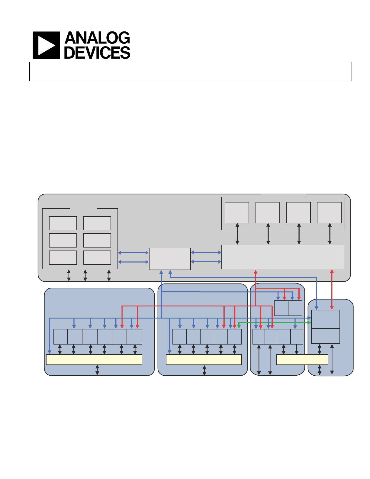
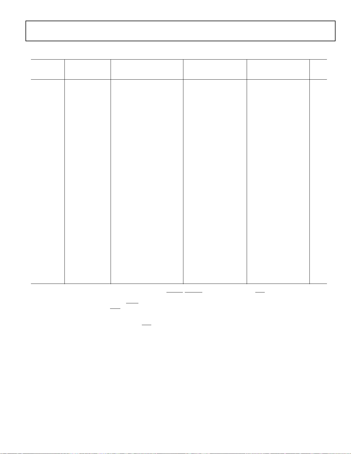
Figure 1. Functional Block Diagram
SHARC and the SHARC logo are registered trademarks of Analog Devices, Inc.
Rev. A
Information furnished by Analog Devices is believed to be accurate and reliable.
However, no responsibility is assumed by Analog Devices for its use, nor for any
infringements of patents or other rights of third parties that may result from its use.
Specifications subject to change without notice. No license is granted by implication
or otherwise under any patent or patent rights of Analog Devices. Trademarks and
registered trademarks are the property of their respective companies.
One Technology Way, P.O. Box 9106, Norwood, MA 02062-9106 U.S.A.
Tel: 781.329.4700 www.analog.com
Fax: 781.326.3113 ©2011 Analog Devices, Inc. All rights reserved.

ADSP-21467/ADSP-21469
TABLE OF CONTENTS
Summary ............................................................... 1
General Description ................................................. 3
Family Core Architecture ........................................ 4
Family Peripheral Architecture ................................ 7
System Design .................................................... 10
Development Tools ............................................. 11
Additional Information ........................................ 11
Related Signal Chains .......................................... 11
Pin Function Descriptions ....................................... 12
Specifications ........................................................ 18
Operating Conditions .......................................... 18
Electrical Characteristics ....................................... 19
Absolute Maximum Ratings .................................. 21
REVISION HISTORY
12/11—Rev. 0 to Rev A
Revised both footnotes in SHARC Family Features .......... 3
Added the ADSP-21467 model with internal ROM.
SHARC Family Features ............................................ 3
Internal Memory Space ............................................. 6
Automotive Products .............................................. 72
Added information on correct pin termination for unused pins
and revised pin descriptions and ball assignments.
Unused Pin Terminations ........................................ 12
Pin Descriptions .................................................... 13
CSP_BGA Ball Assignment—Standard Models ............. 68
Corrected document errata associated with the following specifications.
Pin Function Descriptions ....................................... 12
DDR2 SDRAM Read Cycle Timing ............................ 32
DDR2 SDRAM Write Cycle Timing ........................... 33
AMI Read ............................................................ 34
Added information for shared memory support.
Shared External Memory ........................................... 7
Pin Function Descriptions ....................................... 12
Shared Memory Bus Request .................................... 37
CSP_BGA Ball Assignment—Automotive Models ......... 65
CSP_BGA Ball Assignment—Standard Models ............. 68
Package Information ............................................ 21
ESD Sensitivity ................................................... 22
Timing Specifications ........................................... 22
Test Conditions .................................................. 60
Output Drive Currents ......................................... 60
Capacitive Loading .............................................. 61
Thermal Characteristics ........................................ 63
CSP_BGA Ball Assignment—Automotive Models .......... 65
CSP_BGA Ball Assignment—Standard Models .............. 68
Outline Dimensions ................................................ 71
Surface-Mount Design .......................................... 71
Automotive Products .............................................. 72
Ordering Guide ..................................................... 72
Rev. A | Page 2 of 72 | December 2011
GENERAL DESCRIPTION
ADSP-21467/ADSP-21469
The ADSP-21467/ADSP-21469 SHARC® processors are members of the SIMD SHARC family of DSPs that feature Analog
Devices’ Super Harvard Architecture. The processors are source
code compatible with the ADSP-2126x, ADSP-2136x,
ADSP-2137x, and ADSP-2116x DSPs, as well as with first
generation ADSP-2106x SHARC processors in SISD (singleinstruction, single-data) mode. These 32-bit/40-bit floatingpoint processors are optimized for high performance audio
applications with their large on-chip SRAM, multiple internal
buses to eliminate I/O bottlenecks, and an innovative digital
applications/peripheral interfaces (DAI/DPI).
Table 1 shows performance benchmarks for the processor, and
Table 2 shows the product’s features.
Table 1. Processor Benchmarks
Speed
Benchmark Algorithm
1024 Point Complex FFT (Radix 4, with Reversal) 20.44 s
FIR Filter (Per Tap)
IIR Filter (Per Biquad)
Matrix Multiply (Pipelined)
[3 × 3] × [3 × 1]
[4 × 4] × [4 × 1]
Divide (y/x) 6.67 ns
Inverse Square Root 10.0 ns
1
Assumes two files in multichannel SIMD mode
1
1
(at 450 MHz)
1.11 ns
4.43 ns
10.0 ns
17.78 ns
Table 2. SHARC Family Features
Feature ADSP-21467 ADSP-21469
Maximum Frequency 450 MHz
RAM 5 Mbits
ROM 4 Mbits N/A
Audio Decoders in ROM
DTCP Hardware Accelerator
Pulse-Width Modulation Yes
S/PDIF Yes
DDR2 Memory Interface Yes
DDR2 Memory Bus Width 16 Bits
Shared DDR2 External Memory Yes
Direct DMA from SPORTs to
External Memory Yes
FIR, IIR, FFT Accelerator Yes
MLB Interface Automotive Models Only
IDP Yes
Serial Ports 8
DAI (SRU)/DPI (SRU2) 20/14 pins
UART 1
Link Ports 2
AMI Interface with 8-Bit Support Yes
1
2
Ye s N o
No
Table 2. SHARC Family Features (Continued)
Feature ADSP-21467 ADSP-21469
SPI 2
TWI Yes
SRC Performance –128 dB
Package 324-Ball CSP_BGA
1
Factory programmed ROM includes: Dolby AC-3 5.1 Decode, Dolby Pro Logic IIx,
Dolby Intelligent Mixer (eMix), Dolby Volume postprocessor, Dolby Headphone
v2, DTS Neo:6 and Decode, DTS 5.1 Decode (96/24), Math Tables/Twiddle
Factors/256 and 512 FFT, and ASRC. Please visit www.analog.com for complete
product information and availability.
2
Contact your local Analog Devices sales office for more information regarding
availability of ADSP-21467/ADSP-21469 processors which support DTCP.
Figure 1 on Page 1 shows the two clock domains that make up
the processor. The core clock domain contains the following
features:
• Two processing elements (PEx, PEy), each of which comprises an ALU, multiplier, shifter, and data register file
• Data address generators (DAG1, DAG2)
• Program sequencer with instruction cache
• One periodic interval timer with pinout
• PM and DM buses capable of supporting 2 × 64-bit data
transfers between memory and the core at every core processor cycle
•On-chip SRAM (5 Mbits)
• On-chip mask-programmable ROM (4 Mbits)
• JTAG test access port for emulation and boundary scan.
The JTAG provides software debug through user breakpoints which allows flexible exception handling.
Figure 1 on Page 1 also shows the peripheral clock domain (also
known as the I/O processor) which contains the following
features:
•IOD0 (peripheral DMA) and IOD1 (external port DMA)
buses for 32-bit data transfers
• Peripheral and external port buses for core connection
• External port with an AMI and DDR2 controller
• 4 units for PWM control
• 1 MTM unit for internal-to-internal memory transfers
• Digital applications interface that includes four precision
clock generators (PCG), an input data port (IDP) for serial
and parallel interconnect, an S/PDIF receiver/transmitter,
four asynchronous sample rate converters, eight serial
ports, a flexible signal routing unit (DAI SRU).
• Digital peripheral interface that includes two timers, a 2wire interface, one UART, two serial peripheral interfaces
(SPI), 2 precision clock generators (PCG) and a flexible
signal routing unit (DPI SRU).
Rev. A | Page 3 of 72 | December 2011

ADSP-21467/ADSP-21469
As shown in Figure 1 on Page 1, the processor uses two computational units to deliver a significant performance increase over
the previous SHARC processors on a range of DSP algorithms.
With its SIMD computational hardware, the processors can
perform 2.7 GFLOPS running at 450 MHz and 2.4 GFLOPS
running at 400 MHz.
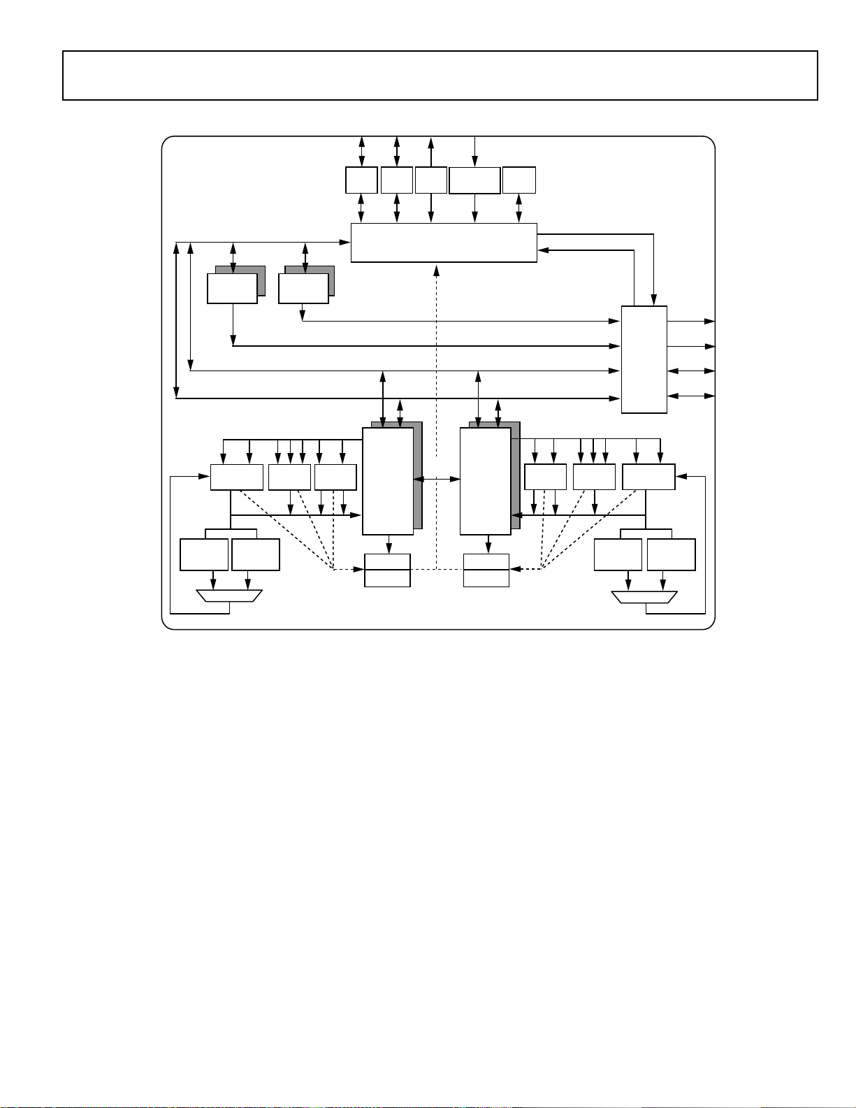
FAMILY CORE ARCHITECTURE
The processors are code compatible at the assembly level with
the ADSP-2137x, ADSP-2136x, ADSP-2126x, ADSP-21160,
and ADSP-21161, and with the first generation ADSP-2106x
SHARC processors. The ADSP-21467/ADSP-21469 processors
share architectural features with the ADSP-2126x, ADSP-2136x,
ADSP-2137x, and ADSP-2116x SIMD SHARC processors, as
shown in Figure 2 and detailed in the following sections.
SIMD Computational Engine
The processor contains two computational processing
elements that operate as a single-instruction, multiple-data
(SIMD) engine. The processing elements are referred to as PEX
and PEY and each contains an ALU, multiplier, shifter, and
register file. PEX is always active, and PEY may be enabled by
setting the PEYEN mode bit in the MODE1 register. When this
mode is enabled, the same instruction is executed in both processing elements, but each processing element operates on
different data. This architecture is efficient at executing math
intensive DSP algorithms.
Entering SIMD mode also has an effect on the way data is transferred between memory and the processing elements. When in
SIMD mode, twice the data bandwidth is required to sustain
computational operation in the processing elements. Because of
this requirement, entering SIMD mode also doubles the bandwidth between memory and the processing elements. When
using the DAGs to transfer data in SIMD mode, two data values
are transferred with each access of memory or the register file.
Independent, Parallel Computation Units
Within each processing element is a set of computational units.
The computational units consist of an arithmetic/logic unit
(ALU), multiplier, and shifter. These units perform all operations in a single cycle. The three units within each processing
element are arranged in parallel, maximizing computational
throughput. Single multifunction instructions execute parallel
ALU and multiplier operations. In SIMD mode, the parallel
ALU and multiplier operations occur in both processing elements. These computation units support IEEE 32-bit singleprecision floating-point, 40-bit extended precision floatingpoint, and 32-bit fixed-point data formats.
Timer
A core timer that can generate periodic software interrupts.
The core timer can be configured to use FLAG3 as a timer
expired signal.
Data Register File
A general-purpose data register file is contained in each processing element. The register files transfer data between the
computation units and the data buses, and store intermediate
results. These 10-port, 32-register (16 primary, 16 secondary)
register files, combined with the processor’s enhanced Harvard
architecture, allow unconstrained data flow between computation units and internal memory. The registers in PEX are
referred to as R0-R15 and in PEY as S0-S15.
Context Switch
Many of the processor’s registers have secondary registers that
can be activated during interrupt servicing for a fast context
switch. The data registers in the register file, the DAG registers,
and the multiplier result registers all have secondary registers.
The primary registers are active at reset, while the secondary
registers are activated by control bits in a mode control register.
Universal Registers
These registers can be used for general-purpose tasks. The
USTAT (4) registers allow easy bit manipulations (Set, Clear,
Toggle, Test, XOR) for all system registers (control/status) of
the core.
The data bus exchange register (PX) permits data to be passed
between the 64-bit PM data bus and the 64-bit DM data bus, or
between the 40-bit register file and the PM/DM data buses.
These registers contain hardware to handle the data width
difference.
Single-Cycle Fetch of Instruction and Four Operands
The processors feature an enhanced Harvard Architecture in
which the data memory (DM) bus transfers data and the program memory (PM) bus transfers both instructions and data
(see Figure 2). With the its separate program and data memory
buses and on-chip instruction cache, the processor can simultaneously fetch four operands (two over each data bus) and one
instruction (from the cache), all in a single cycle.
Instruction Cache
The processors contain an on-chip instruction cache that
enables three-bus operation for fetching an instruction and four
data values. The cache is selective—only the instructions whose
fetches conflict with PM bus data accesses are cached. This
cache allows full speed execution of core, looped operations
such as digital filter multiply-accumulates, and FFT butterfly
processing.
Data Address Generators With Zero-Overhead Hardware Circular Buffer Support
The two data address generators (DAGs) are used for indirect
addressing and implementing circular data buffers in hardware.
Circular buffers allow efficient programming of delay lines and
other data structures required in digital signal processing, and
are commonly used in digital filters and Fourier transforms.
The two DAGs of the processors contain sufficient registers to
allow the creation of up to 32 circular buffers (16 primary
register sets, 16 secondary). The DAGs automatically handle
address pointer wraparound, reduce overhead, increase performance, and simplify implementation. Circular buffers can start
and end at any memory location.
Rev. A | Page 4 of 72 | December 2011
ADSP-21467/ADSP-21469
S
SIMD Core
CACHEINTERRUPT
5 STAGE
PROGRAM SEQUENCER
PM ADDRESS 32
DM ADDRESS 32
DM DATA 64
PM DATA 64
DAG1
16 × 32
MRF
80-BIT
ALU
MULTIPLIER
SHIFTER
RF
Rx/Fx
PEx
16 × 40-BIT
JTAG
DMD/PMD 64
ASTATx
STYKx
ASTATy
STYKy
TIMER
RF
Sx/SFx
PEy
16 × 40-BIT
MRB
80-BIT
MSB
80-BIT
MSF
80-BIT
FLAG
SYSTEM
I/F
US TAT
4 × 32-BIT
PX
64-BIT
DAG2
16 × 32
ALU
MULTIPLIER
SHIFTER
DATA
SWAP
PM ADDRESS 24
PM DATA 48
Flexible Instruction Set
The 48-bit instruction word accommodates a variety of parallel
operations for concise programming. For example, the
processor can conditionally execute a multiply, an add, and a
subtract in both processing elements while branching and fetching up to four 32-bit values from memory—all in a single
instruction.
Variable Instruction Set Architecture (VISA)
In addition to supporting the standard 48-bit instructions from
previous SHARC processors, the processors support new
instructions of 16 and 32 bits. This feature, called Variable
Instruction Set Architecture (VISA), drops redundant/unused
bits within the 48-bit instruction to create more efficient and
compact code. The program sequencer supports fetching these
16-bit and 32-bit instructions from both internal and external
DDR2 memory. Source modules need to be built using the
VISA option in order to allow code generation tools to create
these more efficient opcodes.
Figure 2. SHARC Core Block Diagram
On-Chip Memory
The processors contain 5 Mbits of internal RAM. Each block
can be configured for different combinations of code and data
storage (see Table 4). Each memory block supports single-cycle,
independent accesses by the core processor and I/O processor.
The memory architecture, in combination with its separate onchip buses, allows two data transfers from the core and one
from the I/O processor in a single cycle.
The processor’s SRAM can be configured as a maximum of
160k words of 32-bit data, 320k words of 16-bit data, 106.7k
words of 48-bit instructions (or 40-bit data), or combinations of
different word sizes up to 5 Mbits. All of the memory can be
accessed as 16-bit, 32-bit, 48-bit, or 64-bit words. A 16-bit
floating-point storage format is supported that effectively
doubles the amount of data that may be stored on-chip. Conversion between the 32-bit floating-point and 16-bit floating-point
formats is performed in a single instruction. While each
memory block can store combinations of code and data,
accesses are most efficient when one block stores data using the
DM bus for transfers, and the other block stores instructions
and data using the PM bus for transfers.
Rev. A | Page 5 of 72 | December 2011
ADSP-21467/ADSP-21469
Using the DM bus and PM buses, with one bus dedicated to a
memory block, assures single-cycle execution with two data
transfers. In this case, the instruction must be available in the
cache.
The memory map in Table 3 displays the internal memory
address space of the processors. The 48-bit space section
describes what this address range looks like to an instruction
that retrieves 48-bit memory. The 32-bit section describes what
this address range looks like to an instruction that retrieves 32-
ROM-Based Security
The ROM security feature provides hardware support for securing user software code by preventing unauthorized reading
from the internal code when enabled. When using this feature,
the processors do not boot-load any external code, executing
exclusively from internal ROM. Additionally, the processors are
not freely accessible via the JTAG port. Instead, a unique 64-bit
key, which must be scanned in through the JTAG or Test Access
Port will be assigned to each customer.
bit memory.
Digital Transmission Content Protection
On-Chip Memory Bandwidth
The internal memory architecture allows programs to have four
accesses at the same time to any of the four blocks (assuming
there are no block conflicts). The total bandwidth is realized
using the DMD and PMD buses (2 × 64-bits, CCLK speed) and
the IOD0/1 buses (2 × 32-bit, PCLK speed).
Nonsecured ROM
The DTCP specification defines a cryptographic protocol for
protecting audio entertainment content from illegal copying,
intercepting, and tampering as it traverses high performance
digital buses, such as the IEEE 1394 standard. Only legitimate
entertainment content delivered to a source device via another
approved copy protection system (such as the DVD content
scrambling system) is protected by this copy protection system.
For nonsecured ROM, booting modes are selected using the
BOOTCFG pins as shown in Table 8 on Page 10. In this mode,
emulation is always enabled, and the IVT is placed on the internal RAM except for the case where BOOTCFGx = 011.
Table 3. Internal Memory Space
Long Word (64 Bits)
Block 0 ROM (Reserved)
0x0004 0000–0x0004 7FFF
Reserved
0x0004 8000–0x0004 8FFF
Block 0 SRAM
0x0004 9000–0x0004 EFFF
Reserved
0x0004 F000–0x0004 FFFF
Block 1 ROM (Reserved)
0x0005 0000–0x0005 7FFF
Reserved
0x0005 8000–0x0005 8FFF
Block 1 SRAM
0x0005 9000–0x0005 EFFF
Reserved
0x0005 F000–0x0005 FFFF
Block 2 SRAM
0x0006 0000–0x0006 3FFF
Reserved
0x0006 4000– 0x0006 FFFF
Block 3 SRAM
0x0007 0000–0x0007 3FFF
Reserved
0x0007 4000–0x0007 FFFF
1
Some processors include a customer-definable ROM block. ROM addresses on these models are not reserved as shown in this table. Please contact your Analog Devices sales
representative for additional details.
1
IOP Registers 0x0000 0000–0x0003 FFFF
Extended Precision Normal or
Instruction Word (48 Bits) Normal Word (32 Bits) Short Word (16 Bits)
Block 0 ROM (Reserved)
0x0008 0000–0x0008 AAA9
Reserved
0x0008 AAAA–0x0008 BFFF
Block 0 SRAM
0x0008 C000–0x0009 3FFF
Reserved
0x0009 4000–0x0009 FFFF
Block 1 ROM (Reserved)
0x000A 0000–0x000A AAA9
Reserved
0x000A AAAA–0x000A BFFF
Block 1 SRAM
0x000A C000–0x000B 3FFF
Reserved
0x000B 4000–0x000B FFFF
Block 2 SRAM
0x000C 0000–0x000C 5554
Reserved
0x000C 5555–0x000D FFFF
Block 3 SRAM
0x000E 0000–0x000E 5554
Reserved
0x000E 5555–0x0000F FFFF
Block 0 ROM (Reserved)
0x0008 0000–0x0008 FFFF
Reserved
0x0009 0000–0x0009 1FFF
Block 0 SRAM
0x0009 2000–0x0009 DFFF
Reserved
0x0009 E000–0x0009 FFFF
Block 1 ROM (Reserved)
0x000A 0000–0x000A FFFF
Reserved
0x000B 0000–0x000B 1FFF
Block 1 SRAM
0x000B 2000–0x000B DFFF
Reserved
0x000B E000–0x000B FFFF
Block 2 SRAM
0x000C 0000–0x000C 7FFF
Reserved
0x000C 8000–0x000D FFFF
Block 3 SRAM
0x000E 0000–0x000E 7FFF
Reserved
0x000E 8000–0x000F FFFF
Block 0 ROM (Reserved)
0x0010 0000–0x0011 FFFF
Reserved
0x0012 0000–0x0012 3FFF
Block 0 SRAM
0x0012 4000–0x0013 BFFF
Reserved
0x0013 C000–0x0013 FFFF
Block 1 ROM (Reserved)
0x0014 0000–0x0015 FFFF
Reserved
0x0016 0000–0x0016 3FFF
Block 1 SRAM
0x0016 4000–0x0017 BFFF
Reserved
0x0017 C000–0x0017 FFFF
Block 2 SRAM
0x0018 0000–0x0018 FFFF
Reserved
0x0019 0000–0x001B FFFF
Block 3 SRAM
0x001C 0000–0x001C FFFF
Reserved
0x001D 0000–0x001F FFFF
Rev. A | Page 6 of 72 | December 2011
ADSP-21467/ADSP-21469
FAMILY PERIPHERAL ARCHITECTURE
The processors contain a rich set of peripherals that support a
wide variety of applications including high quality audio, medical imaging, communications, military, test equipment, 3D
graphics, speech recognition, motor control, imaging, and other
applications.
External Port
The external port interface supports access to the external memory through core and DMA accesses. The external memory
address space is divided into four banks. Any bank can be programmed as either asynchronous or synchronous memory. The
external ports are comprised of the following modules.
• An Asynchronous Memory Interface which communicates
with SRAM, Flash, and other devices that meet the standard asynchronous SRAM access protocol. The AMI
supports 2M words of external memory in bank 0 and 4M
words of external memory in bank 1, bank 2, and bank 3.
• A DDR2 DRAM controller. External memory devices up to
2 Gbits in size can be supported.
• Arbitration logic to coordinate core and DMA transfers
between internal and external memory over the external
port.
External Memory
The external port on the processors provide a high performance, glueless interface to a wide variety of industry-standard
memory devices. The external port may be used to interface to
synchronous and/or asynchronous memory devices through the
use of its separate internal DDR2 memory controller. The 16-bit
DDR2 DRAM controller connects to industry-standard synchronous DRAM devices, while the second 8-bit asynchronous
memory controller is intended to interface to a variety of memory devices. Four memory select pins enable up to four separate
devices to coexist, supporting any desired combination of synchronous and asynchronous device types. Non-DDR2 DRAM
external memory address space is shown in Table 4.
Table 4. External Memory for Non-DDR2 DRAM Addresses
Bank Size in Words Address Range
Bank 0 2M 0x0020 0000 – 0x003F FFFF
Bank 1 4M 0x0400 0000 – 0x043F FFFF
Bank 2 4M 0x0800 0000 – 0x083F FFFF
Bank 3 4M 0x0C00 0000 – 0x0C3F FFFF
SIMD Access to External Memory
The DDR2 controller supports SIMD access on the 64-bit EPD
(external port data bus) which allows to access the complementary registers on the PEy unit in the normal word space (NW).
This improves performance since there is no need to explicitly
load the complimentary registers as in SISD mode.
VISA and ISA Access to External Memory
The DDR2 controller also supports VISA code operation which
reduces the memory load since the VISA instructions are compressed. Moreover, bus fetching is reduced because, in the best
case, one 48-bit fetch contains three valid instructions. Code
execution from the traditional ISA operation is also supported.
Note that code execution is only supported from bank 0 regardless of VISA/ISA. Table 5 shows the address ranges for
instruction fetch in each mode.
Table 5. External Bank 0 Instruction Fetch
Access Type Size in Words Address Range
ISA (NW) 4M 0x0020 0000 – 0x005F FFFF
VISA (SW) 10M 0x0060 0000 – 0x00FF FFFF
Shared External Memory
The processors support connection to common shared external
DDR2 memory with other ADSP-2146x processors to create
shared external bus processor systems. This support includes:
• Distributed, on-chip arbitration for the shared external bus
• Fixed and rotating priority bus arbitration
• Bus time-out logic
• Bus lock
Multiple processors can share the external bus with no additional arbitration logic. Arbitration logic is included on-chip to
allow the connection of up to two processors. Table 10 on
Page 13 provides descriptions of the pins used in multiprocessor
systems.
DDR2 Support
The processors support a 16-bit DDR2 interface operating at a
maximum frequency of half the core clock. Execution from
external memory is supported. External memory devices up to
2 Gbits in size can be supported.
DDR2 DRAM Controller
The DDR2 DRAM controller provides a 16-bit interface to up to
four separate banks of industry-standard DDR2 DRAM devices.
Fully compliant with the DDR2 DRAM standard, each bank can
have its own memory select line (DDR2_CS3 – DDR2_CS0),
and can be configured to contain between 32 Mbytes and
256 Mbytes of memory. DDR2 DRAM external memory
address space is shown in Table 6.
A set of programmable timing parameters is available to configure the DDR2 DRAM banks to support memory devices.
Table 6. External Memory for DDR2 DRAM Addresses
Bank Size in Words Address Range
Bank 0 62M 0x0020 0000 – 0x03FF FFFF
Bank 1 64M 0x0400 0000 – 0x07FF FFFF
Bank 2 64M 0x0800 0000 – 0x0BFF FFFF
Bank 3 64M 0x0C00 0000 – 0x0FFF FFFF
Rev. A | Page 7 of 72 | December 2011

ADSP-21467/ADSP-21469
Note that the external memory bank addresses shown are for
normal-word (32-bit) accesses. If 48-bit instructions, as well as
32-bit data, are both placed in the same external memory bank,
care must be taken while mapping them to avoid overlap.
Asynchronous Memory Controller
The asynchronous memory controller provides a configurable
interface for up to four separate banks of memory or I/O
devices. Each bank can be independently programmed with different timing parameters, enabling connection to a wide variety
of memory devices including SRAM, Flash, and EPROM, as well
as I/O devices that interface with standard memory control
lines. Bank 0 occupies a 2M word window and banks 1, 2, and 3
occupy a 4M word window in the processor’s address space but,
if not fully populated, these windows are not made contiguous
by the memory controller logic.
External Port Throughput
The throughput for the external port, based on a 400 MHz
clock, is 66M bytes/s for the AMI and 800M bytes/s for DDR2.
Link Ports
Two 8-bit wide link ports can connect to the link ports of other
DSPs or peripherals. Link ports are bidirectional ports having
eight data lines, an acknowledge line, and a clock line. Link
ports can operate at a maximum frequency of 166 MHz.
MediaLB
The automotive model has a MLB interface which allows the
processors to function as a media local bus device. It includes
support for both 3-pin and 5-pin media local bus protocols. It
supports speeds up to 1024 FS (49.25M bits/sec, FS = 48.1 kHz)
and up to 31 logical channels, with up to 124 bytes of data per
media local bus frame.
The MLB interface supports MOST25 and MOST50 data rates.
The isochronous mode of transfer is not supported.
Pulse-Width Modulation
The PWM module is a flexible, programmable, PWM waveform
generator that can be programmed to generate the required
switching patterns for various applications related to motor and
engine control or audio power control. The PWM generator can
generate either center-aligned or edge-aligned PWM
waveforms. In addition, it can generate complementary signals
on two outputs in paired mode or independent signals in nonpaired mode (applicable to a single group of four PWM
waveforms). The PWM generator is capable of operating in two
distinct modes while generating center-aligned PWM waveforms: single update mode or double update mode.
The entire PWM module has four groups of four PWM outputs
each. Therefore, this module generates 16 PWM outputs in
total. Each PWM group produces two pairs of PWM signals on
the four PWM outputs.
Digital Applications Interface (DAI)
The digital applications interface (DAI) provides the ability to
connect various peripherals to any of the DAI pins
(DAI_P20–1).
Programs make these connections using the signal routing unit
(SRU), shown in Figure 1 on Page 1.
The SRU is a matrix routing unit (or group of multiplexers) that
enables the peripherals provided by the DAI to be interconnected under software control. This allows easy use of the DAI
associated peripherals for a much wider variety of applications
by using a larger set of algorithms than is possible with nonconfigurable signal paths.
The DAI includes the peripherals described in the following
sections.
Serial Ports
The processors feature eight synchronous serial ports that provide an inexpensive interface to a wide variety of digital and
mixed-signal peripheral devices such as Analog Devices’
AD183x family of audio codecs, ADCs, and DACs. The serial
ports are made up of two data lines, a clock, and frame sync. The
data lines can be programmed to either transmit or receive and
each data line has a dedicated DMA channel.
Serial ports can support up to 16 transmit or 16 receive DMA
channels of audio data when all eight SPORTs are enabled, or
four full duplex TDM streams of 128 channels per frame.
The serial ports operate at a maximum data rate of f
Serial port data can be automatically transferred to and from
on-chip memory/external memory via dedicated DMA channels. Each of the serial ports can work in conjunction with
another serial port to provide TDM support. One SPORT provides two transmit signals while the other SPORT provides the
two receive signals. The frame sync and clock are shared.
Serial ports operate in five modes:
• Standard DSP serial mode
•Multichannel (TDM) mode
2
•I
S mode
•Packed I
• Left-justified mode
S/PDIF-Compatible Digital Audio Receiver/Transmitter
The S/PDIF receiver/transmitter has no separate DMA channels. It receives audio data in serial format and converts it into a
biphase encoded signal. The serial data input to the receiver/
transmitter can be formatted as left justified, I
fied with word widths of 16, 18, 20, or 24 bits.
The serial data, clock, and frame sync inputs to the S/PDIF
receiver/transmitter are routed through the signal routing unit
(SRU). They can come from a variety of sources, such as the
SPORTs, external pins, and the precision clock generators
(PCGs), and are controlled by the SRU control registers.
2
S mode
2
S or right justi-
PCLK
/4.
Rev. A | Page 8 of 72 | December 2011

ADSP-21467/ADSP-21469
Asynchronous Sample Rate Converter
The asynchronous sample rate converter (ASRC) contains four
ASRC blocks, is the same core as that used in the AD1896 192
kHz stereo asynchronous sample rate converter, and provides
up to 128 dB SNR. The ASRC block is used to perform synchronous or asynchronous sample rate conversion across
independent stereo channels, without using internal processor
resources. The four SRC blocks can also be configured to operate together to convert multichannel audio data without phase
mismatches. Finally, the ASRC can be used to clean up audio
data from jittery clock sources such as the S/PDIF receiver.
Input Data Port
The IDP provides up to eight serial input channels—each with
its own clock, frame sync, and data inputs. The eight channels
are automatically multiplexed into a single 32-bit by eight-deep
FIFO. Data is always formatted as a 64-bit frame and divided
into two 32-bit words. The serial protocol is designed to receive
audio channels in I
mode. One frame sync cycle indicates one 64-bit left/right pair,
but data is sent to the FIFO as 32-bit words (that is, one-half of a
frame at a time). The processors support 24- and 32-bit I
and 32-bit left-justified, and 24-, 20-, 18- and 16-bit rightjustified formats.
Precision Clock Generators
The precision clock generators (PCG) consist of four units—A,
B, C, and D, each of which generates a pair of signals (clock and
frame sync) derived from a clock input signal. The units are
identical in functionality and operate independently of each
other. The two signals generated by each unit are normally used
as a serial bit clock/frame sync pair.
2
S, left-justified sample pair, or right-justified
2
S, 24-
Digital Peripheral Interface (DPI)
The digital peripheral interface provides connections to two
serial peripheral interface (SPI) ports, one universal asynchronous receiver-transmitter (UART), 12 flags, a 2-wire interface
(TWI), and two general-purpose timers. The DPI includes the
peripherals described in the following sections.
Serial Peripheral Interface
The processors contain two serial peripheral interface ports
(SPI). The SPI is an industry-standard synchronous serial link,
enabling the SPI-compatible port to communicate with other
SPI compatible devices. The SPI consists of two data pins, one
device select pin, and one clock pin. It is a full-duplex
synchronous serial interface, supporting both master and slave
modes. The SPI port can operate in a multimaster environment
by interfacing with up to four other SPI-compatible devices,
either acting as a master or slave device. The SPI-compatible
peripheral implementation also features programmable baud
rate, clock phase, and polarities. The SPI-compatible port uses
open-drain drivers to support a multimaster configuration and
to avoid data contention.
UART Port
The processors provide a full-duplex Universal Asynchronous
Receiver/Transmitter (UART) port, which is fully compatible
with PC-standard UARTs. The UART port provides a simplified UART interface to other peripherals or hosts, supporting
full-duplex, DMA-supported, asynchronous transfers of serial
data. The UART also has multiprocessor communication capability using 9-bit address detection. This allows it to be used in
multidrop networks through the RS-485 data interface
standard. The UART port also includes support for 5 to 8 data
bits, 1 or 2 stop bits, and none, even, or odd parity. The UART
port supports two modes of operation:
• PIO (programmed I/O) – The processors send or receive
data by writing or reading I/O-mapped UART registers.
The data is double-buffered on both transmit and receive.
• DMA (direct memory access) – The DMA controller transfers both transmit and receive data. This reduces the
number and frequency of interrupts required to transfer
data to and from memory.
Ti me rs
The processors have a total of three timers: a core timer that can
generate periodic software interrupts and two generalpurpose timers that can generate periodic interrupts and be
independently set to operate in one of three modes:
•Pulse waveform generation mode
•Pulse width count/capture mode
• External event watchdog mode
The core timer can be configured to use FLAG3 as a timer
expired signal, and each general-purpose timer has one bidirectional pin and four registers that implement its mode of
operation. A single control and status register enables or disables both general-purpose timers independently.
2-Wire Interface Port (TWI)
The TWI is a bidirectional, 2-wire serial bus used to move 8-bit
data while maintaining compliance with the I
The TWI master incorporates the following features:
• 7-bit addressing
• Simultaneous master and slave operation on multiple
device systems with support for multi master data
arbitration
• Digital filtering and timed event processing
• 100 kbps and 400 kbps data rates
• Low interrupt rate
2
C bus protocol.
I/O Processor Features
Automotive versions of the I/O processor provide 67 channels
of DMA, while standard versions provide 36 channels of DMA,
as well as an extensive set of peripherals that are described in the
following sections.
Rev. A | Page 9 of 72 | December 2011
ADSP-21467/ADSP-21469
DMA Controller
The DMA controller allows data transfers without processor
intervention. The DMA controller operates independently and
invisibly to the processor core, allowing DMA operations to
occur while the core is simultaneously executing its program
instructions. DMA transfers can occur between the processor’s
internal memory and its serial ports, the SPI-compatible (serial
peripheral interface) ports, the IDP (input data port), the parallel data acquisition port (PDAP), or the UART.
Up to 67 channels of DMA are available as shown in Table 7.
Programs can be downloaded to the processor using DMA
transfers. Other DMA features include interrupt generation
upon completion of DMA transfers, and DMA chaining for
automatic linked DMA transfers.
Delay Line DMA
Delay line DMA allows processor reads and writes to external
delay line buffers (and hence to external memory) with limited
core interaction.
Scatter/Gather DMA
Scatter/gather DMA allows DMA reads/writes to/from noncontiguous memory blocks.
Table 7. DMA Channels
Peripheral DMA Channels
SPORTs 16
IDP/PDAP 8
SPI 2
UART 2
External Port 2
Link Port 2
Accelerators 2
Memory-to-Memory 2
1
MLB
1
Automotive models only.
31
IIR Accelerator
The IIR (infinite impulse response) accelerator consists of a
1440 word coefficient memory for storage of biquad coefficients, a data memory for storing the intermediate data, and one
MAC unit. A controller manages the accelerator. The IIR accelerator runs at the peripheral clock frequency.
FFT Accelerator
FFT accelerator implements radix-2 complex/real input, complex output FFT with no core intervention. The FFT accelerator
runs at the peripheral clock frequency.
FIR Accelerator
The FIR (finite impulse response) accelerator consists of a 1024
word coefficient memory, a 1024 word deep delay line for the
data, and four MAC units. A controller manages the accelerator.
The FIR accelerator runs at the peripheral clock frequency.
SYSTEM DESIGN
The following sections provide an introduction to system design
options and power supply issues.
Program Booting
The internal memory boots at system power-up from an 8-bit
EPROM via the external port, link port, an SPI master, or an SPI
slave. Booting is determined by the boot configuration
(BOOTCFG2–0) pins in Table 8.
Table 8. Boot Mode Selection
BOOTCFG2–0 Booting Mode
000 SPI Slave Boot
001 SPI Master Boot
010 AMI Boot (for 8-bit Flash boot)
011 No boot occurs, processor executes from
internal ROM after reset
100 Link Port 0 Boot
101 Reserved
The running reset feature allows programs to perform a reset of
the processor core and peripherals, without resetting the PLL
and DDR2 DRAM controller or performing a boot. The
function of the RESETOUT
ing a running reset. For more information, see the ADSP-214xx
SHARC Processor Hardware Reference.
Power Supplies
The processors have separate power supply connections
for the internal (V
) power supplies. The internal and analog supplies must
(V
DD_A
meet the V
the V
DD_EXT
DD_INT
specifications. The external supply must meet
DD_INT
specification. All external supply pins must be con-
nected to the same power supply.
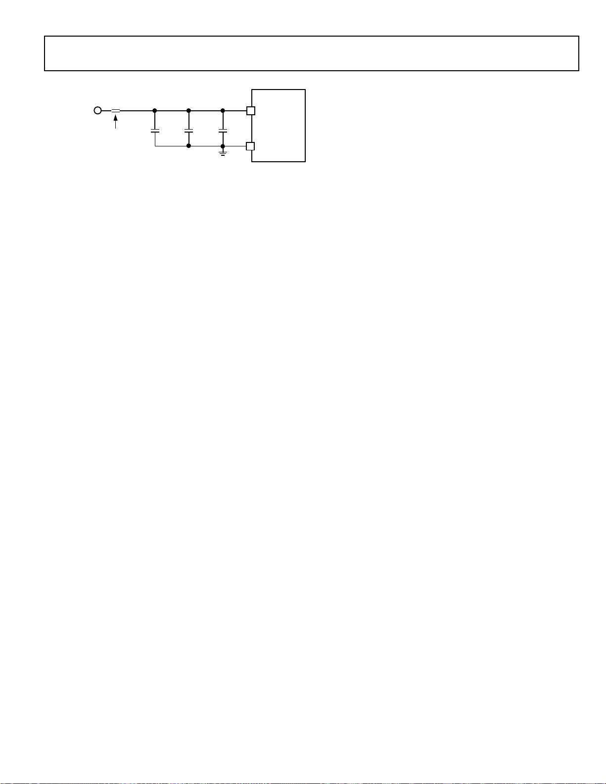
Note that the analog power supply pin (V
cessor’s internal clock generator PLL. To produce a stable clock,
it is recommended that PCB designs use an external filter circuit
for the V
ble to the V
pin. Place the filter components as close as possi-
DD_A
/AGND pins. For an example circuit, see
DD_A
Figure 3. (A recommended ferrite chip is the muRata
BLM18AG102SN1D).
To reduce noise coupling, the PCB should use a parallel pair of
power and ground planes for V
traces to connect the bypass capacitors to the analog power
) and ground (AGND) pins. Note that the V
(V
DD_A
AGND pins specified in Figure 3 are inputs to the processor and
not the analog ground plane on the board—the AGND pin
should connect directly to digital ground (GND) at the chip.
Target Board JTAG Emulator Connector
Analog Devices DSP Tools product line of JTAG emulators uses
the IEEE 1149.1 JTAG test access port of the processor to monitor and control the target board processor during emulation.
Analog Devices DSP Tools product line of JTAG emulators provides emulation at full processor speed, allowing inspection and
pin also acts as the input for initiat-
), external (V
DD_INT
), and analog
DD_EXT
) powers the pro-
DD_A
and GND. Use wide
DD_A
and
Rev. A | Page 10 of 72 | December 2011
HI Z FERRITE
BEAD CHIP
LOCATE ALL COMPONENTS
CLOSE TO VDD_A AND AGND PINS
VDD_A
100nF 10nF 1nF
ADSP-2146x
V
DD_INT
AGND
Figure 3. Analog Power (V
) Filter Circuit
DD_A
modification of memory, registers, and processor stacks. The
processor's JTAG interface ensures that the emulator will not
affect target system loading or timing.
For complete information on Analog Devices’ SHARC DSP
Tools product line of JTAG emulator operation, see the appropriate Emulator Hardware User's Guide.
DEVELOPMENT TOOLS
The processors are supported with a complete set of CROSS-
®
CORE
software and hardware development tools, including
Analog Devices emulators and VisualDSP++
environment. The same emulator hardware that supports other
SHARC processors also fully emulates the ADSP-21467/
ADSP-21469 processors.
EZ-KIT Lite Evaluation Board
For evaluation of the processors, use the EZ-KIT Lite® board
being developed by Analog Devices. The board comes with onchip emulation capabilities and is equipped to enable software
development. Multiple daughter cards are available.
Designing an Emulator-Compatible DSP Board (Target)
The Analog Devices family of emulators are tools that every
DSP developer needs to test and debug hardware and software
systems. Analog Devices has supplied an IEEE 1149.1 JTAG
Test Access Port (TAP) on each JTAG DSP. Nonintrusive incircuit emulation is assured by the use of the processor’s JTAG
interface—the emulator does not affect target system loading or
timing. The emulator uses the TAP to access the internal features of the processor, allowing the developer to load code, set
breakpoints, observe variables, observe memory, and examine
registers. The processor must be halted to send data and
commands, but once an operation has been completed by the
emulator, the DSP system is set running at full speed with no
impact on system timing.
To use these emulators, the target board must include a header
that connects the DSP’s JTAG port to the emulator.
For details on target board design issues including mechanical
layout, single processor connections, signal buffering, signal termination, and emulator pod logic, see the EE-68: Analog Devices
JTAG Emulation Technical Reference on the Analog Devices
website (www.analog.com)—use site search on “EE-68.” This
document is updated regularly to keep pace with improvements
to emulator support.
®
development
ADSP-21467/ADSP-21469
Evaluation Kit
Analog Devices offers a range of EZ-KIT Lite evaluation platforms to use as a cost effective method to learn more about
developing or prototyping applications with Analog Devices
processors, platforms, and software tools. Each EZ-KIT Lite
includes an evaluation board along with an evaluation suite of
the VisualDSP++ development and debugging environment
with the C/C++ compiler, assembler, and linker. Also included
are sample application programs, power supply, and a USB
cable. All evaluation versions of the software tools are limited
for use only with the EZ-KIT Lite product.
The USB controller on the EZ-KIT Lite board connects the
board to the USB port of the user’s PC, enabling the
VisualDSP++ evaluation suite to emulate the on-board processor in-circuit. This permits the customer to download, execute,
and debug programs for the EZ-KIT Lite system. It also allows
in-circuit programming of the on-board Flash device to store
user-specific boot code, enabling the board to run as a standalone unit without being connected to the PC.
With a full version of VisualDSP++ installed (sold separately),
engineers can develop software for the EZ-KIT Lite or any custom defined system. Connecting one of Analog Devices JTAG
emulators to the EZ-KIT Lite board enables high speed, nonintrusive emulation.
ADDITIONAL INFORMATION
This data sheet provides a general overview of the ADSP-21467/
ADSP-21469 architecture and functionality. For detailed information on the core architecture and instruction set, refer to the
SHARC Processor Programming Reference.
RELATED SIGNAL CHAINS
A signal chain is a series of signal-conditioning electronic components that receive input (data acquired from sampling either
real-time phenomena or from stored data) in tandem, with the
output of one portion of the chain supplying input to the next.
Signal chains are often used in signal processing applications to
gather and process data or to apply system controls based on
analysis of real-time phenomena. For more information about
this term and related topics, see the “signal chain” entry in
Wikipedia or the Glossary of EE Terms on the Analog Devices
website.
Analog Devices eases signal processing system development by
providing signal processing components that are designed to
work together well. A tool for viewing relationships between
specific applications and related components is available on the
www.analog.com website.
The Application Signal Chains page in the Circuits from the
TM
Lab
site (http://www.analog.com/signal chains) provides:
• Graphical circuit block diagram presentation of signal
chains for a variety of circuit types and applications
• Drill down links for components in each chain to selection
guides and application information
• Reference designs applying best practice design techniques
Rev. A | Page 11 of 72 | December 2011
ADSP-21467/ADSP-21469
PIN FUNCTION DESCRIPTIONS
Use the termination descriptions in Table 9 when not using the
DDR2 or MLB interfaces.
Warning: System designs must comply with these termination
rules to avoid causing issues of quality, reliability, and power
leakage at these pins.
Table 9. Unused Pin Terminations
Pin Name Unused Termination
DDR2_CKE, DDR2_CS
DDR2_DQSx
DDR2_WE, DDR2_CLKx, DDR2_CLKx
DDR2_ADDR, DDR2_BA, DDR2_DATA
V
DD_DDR2
V
REF
MLBCLK, MLBDAT, MLBSIG, MLBDO, MLBSO Available on automotive models only. In standard products using silicon revision 0.2
1
When the DDR2 controller is not used power down the receive path by setting the PWD bits of the DDR2PADCTLx register.
, DDR2_RAS, DDR2_CAS,
1
, DDR2_DM, DDR2_DQSx,
Leave floating.
Internally three-state by setting the DIS_DDRCTL bit of the DDR2CTL0 register
Connect to the V
Leave floating/unconnected
and above connect to ground (GND). In standard products using silicon revisions
previous to revision 0.2, leave these pins floating if unused.
DD_INT
supply
Rev. A | Page 12 of 72 | December 2011
ADSP-21467/ADSP-21469
Table 10. Pin Descriptions
State Dur ing/ After
Name Type
AMI_ADDR
AMI_DATA
7–0
I/O/T (ipu) High-Z/
23–0
I/O/T (ipu) High-Z External Data. The data pins can be multiplexed to support the external memory
AMI_ACK I (ipu) Memory Acknowledge (AMI_ACK). External devices can deassert AMI_ACK (low) to
AMI_MS
0–1
O/T (ipu) High-Z Memory Select Lines 0–1. These lines are asserted (low) as chip selects for the corre-
AMI_RD O/T (ipu) High-Z AMI Port Read Enable. AMI_RD is asser ted whenever the processor reads a word from
AMI_WR
FLAG[0]/IRQ0
FLAG[1]/IRQ1
FLAG[2]/IRQ2
O/T (ipu) High-Z External Port Write Enable. AMI_WR is asserted when the processor writes a word
I/O (ipu) FLAG[0] INPUT FLAG0/Interrupt Request0.
I/O (ipu) FLAG[1] INPUT FLAG1/Interrupt Request1.
/
I/O (ipu) FLAG[2] INPUT FLAG2/Interrupt Request2/Async Memory Select2.
AMI_MS2
FLAG[3]/TMREXP/
I/O (ipu) FLAG[3] INPUT FLAG3/Timer Expired/Async Memory Select3.
AMI_MS3
The following symbols appear in the Type column of Tab le 10 : A = asynchronous, I =input, O = output, S = synchronous, A/D = active drive,
O/D = open-drain, and T = three-state, ipd = internal pull-down resistor, ipu = internal pull-up resistor.
The internal pull-up (ipu) and internal pull-down (ipd) resistors are d esi gn ed t o h old th e in te rna l p ath fr om t he pi ns a t t he e xpected logic levels.
To pull-up or pull-down the external pads to the expected logic levels, use external resistors. Internal pull-up/pull-down resistors cannot be
enabled/disabled and the value of these resistors cannot be programmed. The range of an ipu resistor can be between 26 k–
63 k. The range of an ipd resistor can be between 31 k–85 k. The three-state voltage of ipu pads will not reach to full the V
typical conditions the voltage is in the range of 2.3 V to 2.7 V.
In this table, the DDR2 pins are SSTL18 compliant. All other pins are LVTTL compliant.
Reset Description
External Address. The processor outputs addresses for external memory and periph-
driven low (boot)
erals on these pins. The data pins can be multiplexed to support the PDAP (I) and PWM
(O). After reset, all AMI_ADDR
FLAG(0–3) pins are in FLAGS mode (default). When configured in the IDP_PDAP_CTL
register, IDP channel 0 scans the AMI_ADDR
AMI pins can be left unconnected.
interface data (I/O), the PDAP (I), FLAGS (I/O) and PWM (O). After reset, all AMI_DATA
pins are in EMIF mode and FLAG(0-3) pins are in FLAGS mode (default). Unused AMI
pins can be left unconnected.
add wait states to an external memory access. AMI_ACK is used by I/O devices,
memory controllers, or other peripherals to hold off completion of an external
memory access. Unused AMI pins can be left unconnected.
sponding banks of external memory on the AMI interface. The MS
memory address lines that change at the same time as the other address lines. When
no external memory access is occurring the MS
however when a conditional memory access instruction is executed, whether or not
the condition is true. Unused AMI pins can be left unconnected. The MS1 pin can be
used in EPORT/FLASH boot mode. For more information, see the ADSP-214xx SHARC
Processor Hardware Reference.
external memory.
to external memory.
pins are in external memory interface mode and
23–0
pins for parallel input data. Unused
23–0
lines are decoded
1-0
lines are inactive; they are active
1-0
DD_EXT
level; at
Rev. A | Page 13 of 72 | December 2011
ADSP-21467/ADSP-21469
Table 10. Pin Descriptions (Continued)
State During/ After
Name Type
DDR2_ADDR
DDR2_BA
2-0
O/T High-Z/
15–0
O/T High-Z/
DDR2_CAS O/T High-Z/
DDR2_CKE O/T High-Z/
DDR2_CS
3-0
DDR2_DATA
DDR2_DM
1-0
DDR2_DQS
DDR2_DQS
DDR2_RAS
DDR2_WE
DDR2_CLK0,
DDR2_CLK0
O/T High-Z/
I/O/T High-Z DDR2 Data In/Out. Connect to corresponding DDR2_DATA pins.
15-0
O/T High-Z/
I/O/T
1-0
(Differential)
1-0
O/T High-Z/
O/T High-Z/
O/T
(Differential)
,
DDR2_CLK1,
DDR2_CLK1
DDR2_ODT O/T High-Z/
The following symbols appear in the Type column of Tab le 10 : A = asynchronous, I =input, O = output, S = synchronous, A/D = active drive,
O/D = open-drain, and T = three-state, ipd = internal pull-down resistor, ipu = internal pull-up resistor.
The internal pull-up (ipu) and internal pull-down (ipd) resistors are de si gned to hol d t he i nt ern al path fr om t he pin s a t th e e xpected logic levels.
To pull-up or pull-down the external pads to the expected logic levels, use external resistors. Internal pull-up/pull-down resistors cannot be
enabled/disabled and the value of these resistors cannot be programmed. The range of an ipu resistor can be between 26 k–
63 k. The range of an ipd resistor can be between 31 k–85 k. The three-state voltage of ipu pads will not reach to full the V
typical conditions the voltage is in the range of 2.3 V to 2.7 V.
In this table, the DDR2 pins are SSTL18 compliant. All other pins are LVTTL compliant.
Reset Description
DDR2 Address. DDR2 address pins.
driven low
DDR2 Bank Address Input. Defines which internal bank an ACTIVATE, READ, WRITE,
driven low
or PRECHARGE command is being applied to. BA
define which mode registers,
2–0
including MR, EMR, EMR( 2), an d EMR(3) are lo aded d uring the LOAD MODE REG ISTER
command.
DDR2 Column Address Strobe. Connect to DDR2_CAS pin; in conjunction with other
driven high
DDR2 command pins, defines the operation for the DDR2 to perform.
DDR2 Clock Enable Output to DDR2. Active high signal. Connect to DDR2 CKE signal.
driven low
driven high
DDR2 Chip Select. All commands are masked when DDR2_CS
DDR2_CS
are decoded memory address lines. Each DDR2_CS
3-0
is driven high.
3-0
line selects the
3-0
corresponding external bank.
DDR2 Input Data Mask. Mask for the DDR2 write data if driven high. Sampled on both
driven high
edges of DDR2_DQS at DDR2 side. DM0 corresponds to DDR2_DATA 7–0 and DM1
corresponds to DDR2_DATA15–8.
High-Z Data Strobe. Output with Write Data. Input with Read Data. DQS0 corresponds to
DDR2_DATA 7–0 and DQS1 corresponds to DDR2_DATA 15–8. Based on software
control via the DDR2CTL3 register, this pin can be single-ended or differential.
DDR2 Row Address Strobe. Connect to DDR2_RAS pin; in conjunction with other
driven high
DDR2 command pins, defines the operation for the DDR2 to perform.
DDR2 Write Enable. Connect to DDR2_WE pin; in conjunction with other DDR2
driven high
High-Z/
driven low
command pins, defines the operation for the DDR2 to perform.
DDR2 Memory Clocks. Two differential outputs available via software control
(DDR2CTL0 register). Free running, minimum frequency not guaranteed during reset.
DDR2 On Die Termination. ODT pin when driven high (along with other require-
driven low
ments) enables the DDR2 termination resistances. ODT is enabled/disabled regardless
of read or write commands.
level; at
DD_EXT
Rev. A | Page 14 of 72 | December 2011

ADSP-21467/ADSP-21469
Table 10. Pin Descriptions (Continued)
State Dur ing/ After
Name Type
DAI _P
20–1
DPI _P
14–1
LDAT0
7–0
LDAT1
7–0
LCLK0
LCLK1
LACK0
LACK1
THD_P I Thermal Diode Anode. If unused, can be left floating.
THD_M O Thermal Diode Cathode. If unused, can be left floating.
MLBCLK I Media Local Bus Clock. This clock is generated by the MLB controller that is synchro-
MLBDAT I/O/T in 3 pin
MLBSIG I/O/T in 3 pin
MLBDO O/T High-Z Media Local Bus Data Output (in 5 pin mode). This pin is used only in 5-pin MLB
MLBSO O/T High-Z Media Local Bus Signal Output (in 5 pin mode). This pin is used only in 5-pin MLB
The following symbols appear in the Type column of Tab le 10 : A = asynchronous, I =input, O = output, S = synchronous, A/D = active drive,
O/D = open-drain, and T = three-state, ipd = internal pull-down resistor, ipu = internal pull-up resistor.
The internal pull-up (ipu) and internal pull-down (ipd) resistors are d esi gn ed t o h old th e in te rna l p ath fr om t he pi ns a t t he e xpected logic levels.
To pull-up or pull-down the external pads to the expected logic levels, use external resistors. Internal pull-up/pull-down resistors cannot be
enabled/disabled and the value of these resistors cannot be programmed. The range of an ipu resistor can be between 26 k–
63 k. The range of an ipd resistor can be between 31 k–85 k. The three-state voltage of ipu pads will not reach to full the V
typical conditions the voltage is in the range of 2.3 V to 2.7 V.
In this table, the DDR2 pins are SSTL18 compliant. All other pins are LVTTL compliant.
I/O/T (ipu) High-Z Digital Applications Interface. These pins provide the physical interface to the DAI
I/O/T (ipu) High-Z Digital Peripheral Interface. These pins provide the physical interface to the DPI SRU.
I/O/T (ipd) High-Z Link Port Data (Link Ports 0–1). When configured as a transmitter, the port drives
I/O/T (ipd) High-Z Link Port Clock (Link Ports 0–1). Allows asynchronous data transfers. When
I/O/T (ipd) High-Z Link Port Acknowledge (Link Port 0–1). Provides handshaking. When the link ports
mode. I/T in 5
pin mode.
mode.
I/T in 5 pin
mode.
Reset Description
SRU. The DAI SRU configuration registers define the combination of on-chip audiocentric peripheral inputs or outputs connected to the pin and to the pin’s output
enable. The configuration registers of these peripherals then determine the exact
behavior of the pin. Any input or output signal present in the DAI SRU may be routed
to any of these pins. The DAI SRU provides the connection from the serial ports, the
S/PDIF module, input data ports (2), and the precision clock generators (4), to the
DAI_P20–1 pins.
The DPI SRU configuration registers define the combination of on-chip peripheral
inputs or outputs connected to the pin and to the pin’s output enable. The configuration registers of these peripherals then determines the exact behavior of the pin.
Any input or output signal present in the DPI SRU may be routed to any of these pins.
The DPI SRU provides the connection from the timers (2), SPIs (2), UART (1), flags (12),
and general-purpose I/O (9) to the DPI_P14–1 pins.
both the data lines.
configured as a transmitter, the port drives LCLKx lines. An external 25 k pull-down
resistor is required for the proper operation of this pin.
are configured as a receiver, the port drives the LACKx line. An external 25 k pulldown resistor is required for the proper operation of this pin.
nized to the MOST network and provides the timing for the entire MLB interface.
49.152 MHz at FS = 48 kHz. If unused, connect to ground (see Tabl e 9 on Pag e 12 ).
High-Z Media Local Bus Data. T he M LB DAT li ne is dr ive n b y t he tr an sm it tin g M LB de vi ce an d
is received by all other MLB devices including the MLB controller. The MLBDAT line
carries the actual data. In 5-pin MLB mode, this pin is an input only. If unused, connect
to ground (see Ta b le 9 o n Page 12).
High-Z Media Local Bus Signal. This is a multiplexed signal which carries the channel/
address generated by the MLB controller, as well as the command and RxStatus bytes
from MLB devices. In 5-pin mode, this pin is an input only. If unused, connect to ground
(see Tab le 9 on Pa ge 12).
mode. This serves as the output data pin in 5-pin mode. If unused, connect to ground
(see Tab le 9 on Pa ge 12).
mode and serves as the output signal pin in 5-pin mode. If unused, connect to ground
(see Tab le 9 on Pa ge 12).
level; at
DD_EXT
Rev. A | Page 15 of 72 | December 2011
ADSP-21467/ADSP-21469
Table 10. Pin Descriptions (Continued)
State During/ After
Name Type
BR
2-1
ID
1-0
TDI I (ipu) Test Data Input (JTAG). Provides serial data for the boundary scan logic.
TDO O /T High-Z Test Data Output (JTAG). Serial scan output of the boundary scan path.
TMS I (ipu) Test Mode Select (JTAG). Used to control the test state machine.
TCK I Test Clock (JTAG). Provides a clock for JTAG boundary scan. The TCK signal must be
TRST
EMU
CLK_CFG
CLKIN I Local Clock In. Used in conjunction with XTAL. CLKIN is the clock input. It configures
XTAL O Crystal Oscillator Terminal. Used in conjunction with CLKIN to drive an external
The following symbols appear in the Type column of Tab le 10 : A = asynchronous, I =input, O = output, S = synchronous, A/D = active drive,
O/D = open-drain, and T = three-state, ipd = internal pull-down resistor, ipu = internal pull-up resistor.
The internal pull-up (ipu) and internal pull-down (ipd) resistors are de si gned to hol d t he i nt ern al path fr om t he pin s a t th e e xpected logic levels.
To pull-up or pull-down the external pads to the expected logic levels, use external resistors. Internal pull-up/pull-down resistors cannot be
enabled/disabled and the value of these resistors cannot be programmed. The range of an ipu resistor can be between 26 k–
63 k. The range of an ipd resistor can be between 31 k–85 k. The three-state voltage of ipu pads will not reach to full the V
typical conditions the voltage is in the range of 2.3 V to 2.7 V.
In this table, the DDR2 pins are SSTL18 compliant. All other pins are LVTTL compliant.
1–0
I/P (ipu) BR1 = driven low by
I Chip ID. Determines which bus request (BR
I (ipu) Test Reset (JTAG). Resets the test state machine. The TRST signal must be asserted
O/D (ipu) High-Z Emulation Status. Must be connected to the ADSP-21467/ADSP-21469 Analog
I Core to CLKIN Ratio Control. These pins set the start up clock frequency. Note that
Reset Description
Bus request. Used by the processor to arbitrate for bus mastership. A processor only
the processor with
(ID1=0, ID0=1)
= driven high by
BR2
the processor with
(ID1=1, ID0=0)
= High-Z if ID
BR2–1
pins are at zero
drives its own BRx
all others. The processor’s own BRx
output.
corresponds to BR1 and ID = 010 corresponds to BR2. Use ID = 000 or 001 in singleprocessor systems. These lines are a system configuration selection that should be
hardwired or only changed at reset. ID = 101, 110, and 111 are reserved.
asserted (pulsed low) after power-up or held low for proper operation of the device.
(pulsed low) after power-up or held low for proper operation of the processor.
Devices DSP Tools product line of JTAG emulators target board connector only.
the operating frequency can be changed by programming the PLL multiplier and
divider in the PMCTL register at any time after the core comes out of reset. The allowed
values are:
00 = 6:1
01 = 32:1
10 = 16:1
11 = reserved
the processor to use either its internal clock generator or an external clock source.
Connecting the necessary components to CLKIN and XTAL enables the internal clock
generator. Connecting the external clock to CLKIN while leaving XTAL unconnected
configures the processor to use the external clock source such as an external clock
oscillator. CLKIN may not be halted, changed, or operated below the specified
frequency.
crystal.
line (corresponding to the value of its ID1–0 inputs) and monitors
line must not be tied high or low because it is an
) is used by the processor. ID = 001
2-1
level; at
DD_EXT
Rev. A | Page 16 of 72 | December 2011
ADSP-21467/ADSP-21469
Table 10. Pin Descriptions (Continued)
State Dur ing/ After
Name Type
RESET I Processor Reset. Resets the processor to a known state. Upon deassertion, there is a
RESETOUT
/
I/O (ipu) Reset Out/Running Reset In. The default setting on this pin is reset out. This pin also
RUNRSTIN
BOOT_CFG
I Boot Configuration Select. These pins select the boot mode for the processor. The
2–0
The following symbols appear in the Type column of Tab le 10 : A = asynchronous, I =input, O = output, S = synchronous, A/D = active drive,
O/D = open-drain, and T = three-state, ipd = internal pull-down resistor, ipu = internal pull-up resistor.
The internal pull-up (ipu) and internal pull-down (ipd) resistors are d esi gn ed t o h old th e in te rna l p ath fr om t he pi ns a t t he e xpected logic levels.
To pull-up or pull-down the external pads to the expected logic levels, use external resistors. Internal pull-up/pull-down resistors cannot be
enabled/disabled and the value of these resistors cannot be programmed. The range of an ipu resistor can be between 26 k–
63 k. The range of an ipd resistor can be between 31 k–85 k. The three-state voltage of ipu pads will not reach to full the V
typical conditions the voltage is in the range of 2.3 V to 2.7 V.
In this table, the DDR2 pins are SSTL18 compliant. All other pins are LVTTL compliant.
Table 11. Pin List, Power and Ground
Reset Description
4096 CLKIN cycle latency for the PLL to lock. After this time, the core begins program
execution from the hardware reset vector address. The RESET
(low) at power-up.
has a second function as RUNRSTIN which is enabled by setting bit 0 of the RUNRSTCTL
register. For more information, see the ADSP-214xx SHARC Processor Hardware
Reference.
BOOT_CFG pins must be valid before RESET
input must be asserted
(hardware and software) is de-asserted.
level; at
DD_EXT
Name Type Description
V
DD_INT
V
DD_EXT
V
DD_A
V
DD_THD
V
DD_DDR2
V
REF
1
PDDR2 Interface Power
PInternal Power
PExternal Power
PAnalog Power for PLL
PThermal Diode Power
PDDR2 Input Voltage Reference
GND G Ground
AGND G Analog Ground
1
Applies to DDR2 signals.
Rev. A | Page 17 of 72 | December 2011

ADSP-21467/ADSP-21469
SPECIFICATIONS
OPERATING CONDITIONS
450 MHz 400 MHz
1
Description Min Nom Max Min Nom Max
V
DD_INT
V
DD_EXT
2
V
DD_A
V
DD_DDR2
V
DD_THD
V
REF
5
V
IH
5
V
Low Level Input Voltage @
IL
V
IH_CLKIN
6
V
IL_CLKIN
V
(DC) DC Low Level Input Voltage V
IL_DDR2
V
IH_DDR2
V
(AC) AC Low Level Input Voltage V
IL_DDR2
V
IH_DDR2
T
J
Internal (Core) Supply Voltage 1.05 1.1 1.15 1.0 1.05 1.1 V
External (I/O) Supply Voltage 3.13 3.3 3.47 3.13 3.3 3.47 V
Analog Power Supply Voltage 1.05 1.1 1.15 1.0 1.05 1.1 V
3, 4
DDR2 Controller Supply Voltage 1.7 1.8 1.9 1.7 1.8 1.9 V
Thermal Diode Supply Voltage 3.13 3.3 3.47 3.13 3.3 3.47 V
DDR2 Reference Voltage 0.84 0.9 0.96 0.84 0.9 0.96 V
High Level Input Voltage @
= Max
V
DD_EXT
2.0 2.0 V
0.8 0.8 V
V
= Min
6
(DC) DC High Level Input Voltage V
(AC) AC High Level Input Voltage V
DD_EXT
High Level Input Voltage @
= Max
V
DD_EXT
Low Level Input Voltage @
V
= Min
DD_EXT
Junction Temperature 324-Lead
CSP_BGA @ T
AMBIENT
0°C to
2.0 2.0 V
1.32 1.32 V
– 0.125 V
REF
+ 0.125 V
REF
– 0.25 V
REF
+ 0.25 V
REF
+ 0.125 V
REF
+ 0.25 V
REF
0 115 0 110 °C
– 0.125 V
REF
– 0.25 V
REF
+70°C
T
J
Junction Temperature 324-Lead
CSP_BGA @ T
AMBIENT
–40°C to
N/A N/A –40 125 °C
+85°C
1
Specifications subject to change without notice.
2
See Figure 3 on Page 11 for an example filter circuit.
3
Applies to DDR2 signals.
4
If unused, see Table 9 on Page 12.
5
Applies to input and bidirectional pins: AMI_ADDR23–0, AMI_DATA7–0, FLAG3–0, DAI_Px, DPI_Px, BOOTCFGx, CLKCFGx, (RUNRSTIN), RESET, TCK, TMS, TDI,
TRST.
6
Applies to input pin CLKIN.
UnitParameter
Rev. A | Page 18 of 72 | December 2011
ADSP-21467/ADSP-21469
ELECTRICAL CHARACTERISTICS
450 MHz 400 MHz
1
Description Test Conditions Min Max Min Max
2
V
OH
2
V
OL
V
OH_DDR2
V
OL_DDR2
4, 5
I
IH
4, 6
I
IL
5
I
ILPU
6
I
IHPD
7, 8
I
OZH
7, 9
I
Three-State Leakage
OZL
8
I
OZLPU
9
I
OZHPD
I
DD-INTYP
11
I
DD_A
12, 13
C
IN
1
Specifications subject to change without notice.
2
Applies to output and bidirectional pins: AMI_ADDR23-0, AMI_DATA7-0, AMI_RD, AMI_WR, FLAG3–0, DAI_Px, DPI_Px, EMU, TDO.
3
See Output Drive Currents on Page 60 for typical drive current capabilities.
4
Applies to input pins: BOOTCFGx, CLKCFGx, TCK, RESET, CLKIN.
5
Applies to input pins with internal pull-ups: TRST, TMS, TDI.
6
Applies to input pins with internal pull-downs: MLBCLK
7
Applies to three-statable pins: all DDR2 pins.
8
Applies to three-statable pins with pull-ups: DAI_Px, DPI_Px, EMU.
9
Applies to three-statable pins with pull-downs: MLBDAT, MLBSIG, MLBDO, MLBSO, LDAT07-0, LDAT17-0, LCLK0, LCLK1, LACK0, LACK1.
10
See Engineer-to-Engineer Note EE-348 “Estimating Power Dissipation for ADSP-2146x SHARC Processors” for further information.
11
Characterized but not tested.
12
Applies to all signal pins.
13
Guaranteed, but not tested.
High Level Output
Voltage
Low Level Output
Voltage
High Level Output
Voltage for DDR2
Low Level Output
Voltage for DDR2
High Level Input
Current
Low Level Input
Current
Low Level Input
Current Pull-up
High Level Input
Current Pull-down
Three-State Leakage
Current
Current
Three-State Leakage
Current Pull-up
Three-State Leakage
Current Pull-down
10
Supply Current
(Internal)
Supply Current
(Analog)
Input Capacitance T
@ V
@ V
@ V
@ V
@ V
V
IN
@ V
@ V
@ V
V
IN
@ V
VIN = V
@ V
= Min, IOH = –1.0 mA32.4 2.4 V
DD_EXT
Max
3
0.4 0.4 V
10 10 μA
200 200 μA
10 10 μA
10 10 μA
= Min, IOL = 1.0 mA
DD_EXT
= Min, IOH = –13.4 mA 1.4 1.4 V
DD_DDR
= Min, IOL = 13.4 mA 0.29 0.29 V
DD_DDR
= Max,
DD_EXT
= V
DD_EXT
DD_EXT
DD_EXT
= V
DD_EXT/VDD_DDR
DD_EXT/VDD_DDR
Max
DD_EXT
= Max, VIN = 0 V 10 10 μA
= Max, VIN = 0 V 200 200 μA
= Max,
Max
DD_EXT
= Max,
DD_EXT/VDD_DDR
= Max,
VIN = 0 V
@ V
@ V
VIN = V
f
CCLK
V
DD_A
CASE
= Max, VIN = 0 V 200 200 μA
DD_EXT
= Max,
DD_EXT
DD_EXT
Max
> 0 MHz Tab le 13 +
200 200 μA
Ta ble 1 3 +
Tab le 14 × ASF
Ta ble 1 4 × ASF
= Max 10 10 mA
= 25°C 5 5 pF
UnitParameter
mA
Rev. A | Page 19 of 72 | December 2011
ADSP-21467/ADSP-21469
Total Power Dissipation
Total power dissipation has two components:
1. Internal power consumption
2. External power consumption
Internal power consumption also comprises two components:
1. Static, due to leakage current. Table 13 shows the static current consumption (I
temperature (T
2. Dynamic (I
DD-DYNAMC
DD-STATIC
) and core voltage (V
J
acteristics and activity level of the processor. The activity
level is reflected by the Activity Scaling Factor (ASF), which
represents application code running on the processor core
and having various levels of peripheral and external port
activity (Table 12). Dynamic current consumption is calculated by scaling the specific application by the ASF and
using baseline dynamic current consumption as a
reference.
) as a function of junction
).
DD_INT
), due to transistor switching char-
The ASF is combined with the CCLK frequency and V
DD_INT
dependent data in Table 14 to calculate this part. External power
consumption is due to the switching activity of the external
pins.
Table 12. Activity Scaling Factors (ASF)
1
Activity Scaling Factor (ASF)
Idle 0.38
Low 0.58
High 1.23
Peak 1.35
Peak-typical (50:50)
2
0.87
Peak-typical (60:40) 0.94
Peak-typical (70:30) 1.00
1
See Estimating Power for SHARC Processors (EE-348) for more information on
the explanation of the power vectors specific to the ASF table.
2
Ratio of continuous instruction loop (core) to DDR2 control code; reads:writes.
Table 13. I
1
TJ (°C)
DD-STATIC
(mA)
(V)
1
V
DD_INT
0.95 V 1.0 V 1.05 V 1.10 V 1.15 V
–45 72 91 110 140 167
–35 79 99 119 149 181
–25 89 109 131 163 198
–15 101 122 145 182 220
–5 115 140 166 206 249
5 134 162 192 237 284
15 158 189 223 273 326
25 186 222 260 318 377
35 218 259 302 367 434
45 258 305 354 428 503
55 305 359 413 497 582
65 360 421 484 578 675
75 424 496 566 674 781
85 502 580 660 783 904
95 586 683 768 912 1048
105 692 794 896 1054 1212
115 806 921 1036 1220 1394
125 939 1070 1198 1404 1601
1
Valid temperature and voltage ranges are model-specific. See Operating Conditions on Page 18.
Rev. A | Page 20 of 72 | December 2011
ADSP-21467/ADSP-21469
vvvvvv.x n.n
tppZ-cc
S
ADSP-2146x
a
yyww country_of_origin
Table 14. Baseline Dynamic Current in CCLK Domain (mA, with ASF = 1.0)
f
CCLK
(MHz)
2
0.95 V 1.0 V 1.05 V 1.10 V 1.15 V
Voltage (V
1
DD_INT
2
)
1007882869198
150 115 121 130 136 142
200 150 159 169 177 188
250 186 197 208 219 231
300 222 236 249 261 276
350 259 275 288 304 319
400 293 309 328 344 361
450 N/A N/A 366 385 406
1
The values are not guaranteed as standalone maximum specifications. They must be combined with static current per the equations of Electrical Characteristics on Page 19.
2
Valid frequency and voltage ranges are model-specific. See Operating Conditions on Page 18.
ABSOLUTE MAXIMUM RATINGS
Stresses greater than those listed in Table 15 may cause permanent damage to the device. These are stress ratings only;
functional operation of the device at these or any other conditions greater than those indicated in the operational sections of
PACKAGE INFORMATION
The information presented in Figure 4 and Table 16 provides
details about the package branding for the processor. For a complete listing of product availability, see Ordering Guide on
Page 72.
this specification is not implied. Exposure to absolute maximum
rating conditions for extended periods may affect device
reliability.
Table 15. Absolute Maximum Ratings
Parameter Rating
Internal (Core) Supply Voltage (V
Analog (PLL) Supply Voltage (V
External (I/O) Supply Voltage (V
Thermal Diode Supply Voltage
(V
DD_THD
)
DDR2 Controller Supply Voltage
(V
DD_DDR2)
) –0.3 V to +1.32 V
DD_INT
) –0.3 V to +1.15 V
DD_A
) –0.3 V to +3.6 V
DD_EXT
–0.3 V to +3.6 V
–0.3 V to +1.9 V
DDR2 Input Voltage –0.3 V to +1.9 V
Input Voltage –0.3 V to +3.6 V
Output Voltage Swing –0.3 V to V
DD_EXT
Storage Temperature Range –65C to +150C
Junction Temperature While Biased 125C
+0.5 V
Figure 4. Typical Package Brand
Table 16. Package Brand Information
1
Brand Key Field Description
t Temperature Range
pp Package Type
Z RoHS Compliant Option
cc See Ordering Guide
vvvvvv.x Assembly Lot Code
n.n Silicon Revision
# RoHS Compliant Designation
yyww Date Code
1
Non-automotive only. For branding information specific to automotive
products, contact Analog Devices, Inc.
Rev. A | Page 21 of 72 | December 2011
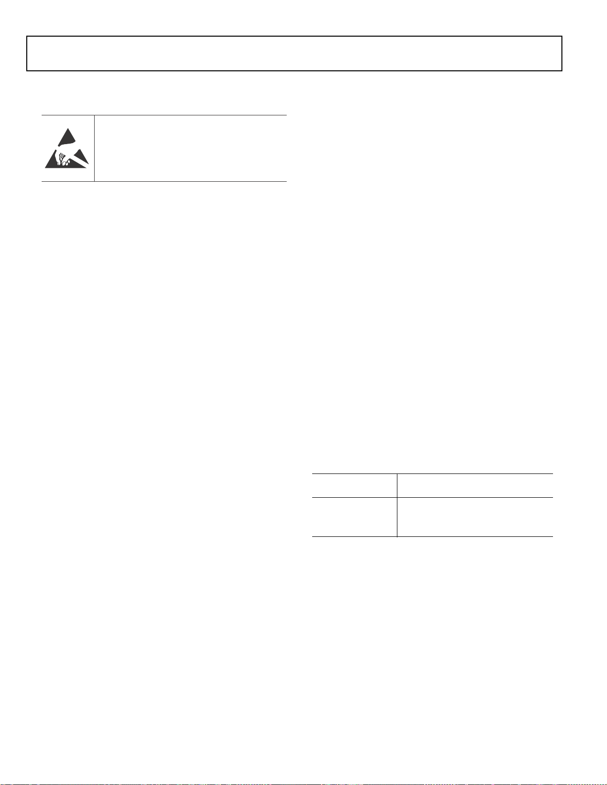
ADSP-21467/ADSP-21469
ESD
(electrostatic discharge) sensitive device.
Charged devices and circuit boards can discharge
without detection. Although this product features
patented or proprietary protection circuitry, damage
may occur on devices subjected to high energy ESD.
Therefore, proper ESD precautions should be taken to
avoid
performance degradation or loss of functionality.
ESD SENSITIVITY
TIMING SPECIFICATIONS
Use the exact timing information given. Do not attempt to
derive parameters from the addition or subtraction of others.
While addition or subtraction would yield meaningful results
for an individual device, the values given in this data sheet
reflect statistical variations and worst cases. Consequently, it is
not meaningful to add parameters to derive longer times. See
Figure 46 on Page 60 under Test Conditions for voltage refer-
ence levels.
In the following sections, Switching Characteristics specify how
the processor changes its signals. Circuitry external to the processor must be designed for compatibility with these signal
characteristics. Switching characteristics describe what the processor will do in a given circumstance. Use switching
characteristics to ensure that any timing requirement of a device
connected to the processor (such as memory) is satisfied.
In the following sections, Timing Requirements apply to signals
that are controlled by circuitry external to the processor, such as
the data input for a read operation. Timing requirements guarantee that the processor operates correctly with other devices.
Core Clock Requirements
The processor’s internal clock (a multiple of CLKIN) provides
the clock signal for timing internal memory, processor core, and
serial ports. During reset, program the ratio between the processor’s internal clock frequency and external (CLKIN) clock
frequency with the CLK_CFG1–0 pins.
The processor’s internal clock switches at higher frequencies
than the system input clock (CLKIN). To generate the internal
clock, the processor uses an internal phase-locked loop (PLL,
see Figure 5). This PLL-based clocking minimizes the skew
between the system clock (CLKIN) signal and the processor’s
internal clock.
Voltage Controlled Oscillator (VCO)
In application designs, the PLL multiplier value should be
selected in such a way that the VCO frequency never exceeds
f
specified in Table 19.
VCO
• The product of CLKIN and PLLM must never exceed 1/2 of
f
(max) in Table 19 if the input divider is not enabled
VCO
(INDIV = 0).
• The product of CLKIN and PLLM must never exceed
f
(max) in Table 19 if the input divider is enabled
VCO
(INDIV = 1).
The VCO frequency is calculated as follows:
f
= 2 × PLLM × f
VCO
f
= (2 × PLLM × f
CCLK
INPUT
INPUT
) ÷ (PLLD)
where:
f
= VCO output
VCO
PLLM = Multiplier value programmed in the PMCTL register.
During reset, the PLLM value is derived from the ratio selected
using the CLK_CFG pins in hardware.
PLLD = Divider value 2, 4, 8, or 16 based on the PLLD value
programmed on the PMCTL register. During reset this value
is 2.
f
= input frequency to the PLL
INPUT
f
= CLKIN when the input divider is disabled, or
INPUT
f
= CLKIN 2 when the input divider is enabled
INPUT
Note the definitions of the clock periods that are a function of
CLKIN and the appropriate ratio control shown in and
Table 17. All of the timing specifications for the peripherals are
defined in relation to t
. See the peripheral specific section
PCLK
for each peripheral’s timing information.
Table 17. Clock Periods
Timing
Requirements Description
t
CK
t
CCLK
t
PCLK
CLKIN Clock Period
Processor Core Clock Period
Peripheral Clock Period = 2 × t
CCLK
Figure 5 shows core to CLKIN relationships with external oscil-
lator or crystal. The shaded divider/multiplier blocks denote
where clock ratios can be set through hardware or software
using the power management control register (PMCTL). For
more information, see the ADSP-214xx SHARC Processor Hard-
ware Reference.
Rev. A | Page 22 of 72 | December 2011

ADSP-21467/ADSP-21469
CLKIN
PCLK
DDR2_CLK
DDR2
DIVIDER
B
YP
A
S
S
MU
X
DIVIDE
BY 2
CCLK
BY
P
A
S
S
M
U
X
XTAL
CLKIN
DIVIDER
RESETOUT
RESET
BUF
BUF
PLLI
CLK
PIN MUX
RESETOUT
CLKOUT (TEST ONLY)
DELAY OF
4096 CLKIN
CYCLES
CORERST
CCLK
PCLK
CLK_CFGx/
PMCTL
LINK PORT
CLOCK
DIVIDER
LCLK
B
Y
P
A
S
S
M
U
X
PMCTL
(PLLBP)
PMCTL
(PLLBP)
PMCTL
(INDIV)
PMCTL
(LCLKR)
PMCTL
(DDR2CKR)
f
INPUT
f
CCLK
LOOP
FILTER
PLL
f
VCO
÷ (2 × PLLM)
VCO
PLL
DIVIDER
PMCTL
(PLLD)
f
VCO
CLK_CFGx/
PMCTL (2 × PLLM)
Figure 5. Core Clock and System Clock Relationship to CLKIN
Rev. A | Page 23 of 72 | December 2011

ADSP-21467/ADSP-21469
t
RSTVDD
t
CLKVDD
t
CLKRST
t
CORERST
t
PLLRST
V
DDEXT
V
DDINT
CLKIN
CLK_CFG1–0
RESET
RESETOUT
t
IVDDEVDD
Power-Up Sequencing
The timing requirements for processor startup are given in
Table 18. While no specific power-up sequencing is required
between V
DD_EXT
, V
DD_DDR2
, and V
, there are some con-
DD_INT
siderations that system designs should take into account.
• No power supply should be powered up for an extended
period of time (> 200 ms) before another supply starts to
ramp up.
•If V
such as RESETOUT
momentarily until the V
power supply comes up after V
DD_INT
and RESET, may actually drive
DD_INT
, any pin,
DD_EXT
rail has powered up.
Table 18. Power-Up Sequencing Timing Requirements (Processor Startup)
Parameter Min Max Unit
Timing Requirements
t
RSTVDD
t
IVDD-EVDD
t
EVDD_DDR2VDD
1
t
CLKVDD
t
CLKRST
t
PLLRST
RESET Low Before V
V
On Before V
DD_INT
V
On Before V
DD_EXT
CLKIN Valid After V
DD_INT
DD_EXT
DD_DDR2
DD_INT
or V
or V
DD_EXT
DD_EXT
or V
or V
DD_DDR2
DD_DDR2
CLKIN Valid Before RESET Deasserted 10
PLL Control Setup Before RESET Deasserted 20
Switching Characteristic
t
CORERST
1
Valid V
design of the power supply subsystem.
2
Assumes a stable CLKIN signal, after meeting worst-case startup timing of crystal oscillators. Refer to your crystal oscillator manufacturer's data sheet for startup time. Assume
a 25 ms maximum oscillator startup time if using the XTAL pin and internal oscillator circuit in conjunction with an external crystal.
3
Based on CLKIN cycles.
4
Applies after the power-up sequence is complete. Subsequent resets require a minimum of four CLKIN cycles for RESET to be held low in order to properly initialize and
propagate default states at all I/O pins.
5
The 4096 cycle count depends on t
cycles maximum.
assumes that the supply is fully ramped to its nominal value. Voltage ramp rates can vary from microseconds to hundreds of milliseconds depending on the
DD_INT
Core Reset Deasserted After RESET Deasserted 4096 × tCK + 2 × t
specification in Table 20. If setup time is not met, one additional CLKIN cycle may be added to the core reset time, resulting in 4097
SRST
Systems sharing these signals on the board must determine
if there are any issues that need to be addressed based on
this behavior.
Note that during power-up, when the V
comes up after V
, a leakage current of the order of three-
DD_EXT
DD_INT
power supply
state leakage current pull-up, pull-down may be observed on
any pin, even if that pin is an input only (for example the RESET
pin) until the V
rail has powered up.
DD_INT
On 0 ms
–200 +200 ms
–200 +200 ms
Valid 0 200 ms
2
3
5
4,
CCLK
ms
ms
ms
Figure 6. Power-Up Sequencing
Rev. A | Page 24 of 72 | December 2011

Clock Input
CLKIN
t
CK
t
CKL
t
CKH
t
CKJ
C1
22pF
Y1
R1
1M: *
XTAL
CLKIN
C2
22pF
25.000 MHz
R2
47: *
R2 SHOULD BE CHOSEN TO LIMIT CRYSTAL
DRIVE POW ER. REFER T O CRYSTAL
MANUFACTURER’S SPECIFICATIONS
*TYPICAL VALUES
ADSP-2146x
Table 19. Clock Input
Parameter
Timing Requirements
t
CK
t
CKL
t
CKH
t
CKRF
t
CCLK
6
f
VCO
7, 8
t
CKJ
1
Applies to all 400 MHz models. See Ordering Guide on Page 72.
2
Applies to all 450 MHz models. See Ordering Guide on Page 72.
3
Applies only for CLK_CFG1–0 = 00 and default values for PLL control bits in PMCTL.
4
Guaranteed by simulation but not tested on silicon.
5
Any changes to PLL control bits in the PMCTL register must meet core clock timing specification t
6
See Figure 5 on Page 23 for VCO diagram.
7
Actual input jitter should be combined with ac specifications for accurate timing analysis.
8
Jitter specification is maximum peak-to-peak time interval error (TIE) jitter.
CLKIN Period 15
CLKIN Width Low 7.5 45 6.63 45 ns
CLKIN Width High 7.5 45 6.63 45 ns
CLKIN Rise/Fall (0.4 V to 2.0 V) 3
5
CCLK Period 2.5 10 2.22 10 ns
VCO Frequency 200 900 200 900 MHz
CLKIN Jitter Tolerance –250 +250 –250 +250 ps
3
ADSP-21467/ADSP-21469
400 MHz
1
450 MHz
100 13.26 100 ns
CCLK
4
.
34ns
2
UnitMin Max Min Max
Figure 7. Clock Input
Clock Signals
The processor can use an external clock or a crystal. See the
CLKIN pin description in Table 10. Programs can configure the
processor to use its internal clock generator by connecting the
necessary components to CLKIN and XTAL. Figure 8 shows the
component connections used for a crystal operating in fundamental mode. Note that the clock rate is achieved using a
25 MHz crystal and a PLL multiplier ratio 16:1 (CCLK:CLKIN
achieves a clock speed of 400 MHz).
To achieve the full core clock rate, programs need to configure
the multiplier bits in the PMCTL register.
Figure 8. Recommended Circuit for
Fundamental Mode Crystal Operation
Rev. A | Page 25 of 72 | December 2011

ADSP-21467/ADSP-21469
CLKIN
RESET
t
SRST
t
WRST
CLKIN
RUNRSTIN
t
WRUNRST
t
SRUNRST
Reset
Table 20. Reset
Parameter Min Max Unit
Timing Requirements
1
t
WRST
t
SRST
1
Applies after the power-up sequence is complete. At power-up, the processor’s internal phase-locked loop requires no more than 100 s while RESET is low, assuming stable
VDD and CLKIN (not including start-up time of external clock oscillator).
Running Reset
The following timing specification applies to
RESETOUT
RUNRSTIN
RESET Pulse Width Low 4 × t
CK
RESET Setup Before CLKIN Low 8 ns
Figure 9. Reset
/RUNRSTIN pin when it is configured as
.
ns
Table 21. Running Reset
Parameter Min Max Unit
Timing Requirements
t
WRUNRST
t
SRUNRST
Running RESET Pulse Width Low 4 × t
CK
ns
Running RESET Setup Before CLKIN High 8 ns
Figure 10. Running Reset
Rev. A | Page 26 of 72 | December 2011

ADSP-21467/ADSP-21469
INTERRUPT
INPUTS
t
IPW
FLAG3
(TMREXP)
t
WCTIM
Interrupts
The following timing specification applies to the FLAG0,
FLAG1, and FLAG2 pins when they are configured as IRQ0
, and IRQ2 interrupts as well as the DAI_P20–1 and
IRQ1
DPI_P14–1 pins when they are configured as interrupts.
Table 22. Interrupts
Parameter Min Max Unit
Timing Requirement
t
IPW
IRQx Pulse Width 2 × t
Core Timer
The following timing specification applies to FLAG3 when it is
configured as the core timer (TMREXP).
,
+ 2 ns
PCLK
Figure 11. Interrupts
Table 23. Core Timer
Parameter Min Max Unit
Switching Characteristic
t
WCTIM
TMREXP Pulse Width 4 × t
Figure 12. Core Timer
– 1 ns
PCLK
Rev. A | Page 27 of 72 | December 2011

ADSP-21467/ADSP-21469
PWM
OUTPUTS
t
PWMO
TIMER
CAPTURE
INPUTS
t
PWI
Timer PWM_OUT Cycle Timing
The following timing specification applies to Timer0 and
Timer1 in PWM_OUT (pulse-width modulation) mode. Timer
signals are routed to the DPI_P14–1 pins through the DPI SRU.
Therefore, the timing specifications provided below are valid at
the DPI_P14–1 pins.
Table 24. Timer PWM_OUT Timing
Parameter Min Max Unit
Switching Characteristic
t
PWMO
Timer WDTH_CAP Timing
The following timing specification applies to Timer0 and
Timer1 in WDTH_CAP (pulse width count and capture) mode.
Timer signals are routed to the DPI_P14–1 pins through the
SRU. Therefore, the timing specifications provided below are
valid at the DPI_P14–1 pins.
Timer Pulse Width Output 2 × t
Figure 13. Timer PWM_OUT Timing
– 1.2 2 × (231 – 1) × t
PCLK
PCLK
ns
Table 25. Timer Width Capture Timing
Parameter Min Max Unit
Timing Requirement
t
PWI
Timer Pulse Width 2 × t
Figure 14. Timer Width Capture Timing
2 × (231 – 1) × t
PCLK
PCLK
ns
Rev. A | Page 28 of 72 | December 2011

ADSP-21467/ADSP-21469
DAI_Pn
DPI_Pn
DAI_Pm
DPI_Pm
t
DPIO
Pin to Pin Direct Routing (DAI and DPI)
For direct pin connections only (for example DAI_PB01_I to
DAI_PB02_O).
Table 26. DAI and DPI Pin to Pin Routing
Parameter Min Max Unit
Timing Requirement
t
DPIO
Delay DAI/DPI Pin Input Valid to DAI/DPI Output Valid 1.5 12 ns
Figure 15. DAI and DPI Pin to Pin Direct Routing
Rev. A | Page 29 of 72 | December 2011

ADSP-21467/ADSP-21469
DAI_Pn
DPI_Pn
PCG_TRIGx_I
DAI_Pm
DPI_Pm
PCG_EXTx_I
(CLKIN)
DAI_Py
DPI_Py
PCK_CLKx_O
DAI_Pz
DPI_Pz
PCG_FSx_O
t
DTRIGFS
t
DTRIGCLK
t
DPCGIO
t
STRIG
t
HTRIG
t
PCGOW
t
DPCGIO
t
PCGIP
Precision Clock Generator (Direct Pin Routing)
This timing is only valid when the SRU is configured such that
the precision clock generator (PCG) takes its inputs directly
from the DAI pins (via pin buffers) and sends its outputs
inputs and outputs are not directly routed to/from DAI pins (via
pin buffers) there is no timing data available. All timing parameters and switching characteristics apply to external DAI pins
(DAI_P01 – DAI_P20).
directly to the DAI pins. For the other cases, where the PCG’s
Table 27. Precision Clock Generator (Direct Pin Routing)
Parameter Min Max Unit
Timing Requirements
t
PCGIW
t
STRIG
Input Clock Period t
PCG Trigger Setup Before Falling Edge of PCG Input
× 4 ns
PCLK
4.5 ns
Clock
t
HTRIG
PCG Trigger Hold After Falling Edge of PCG Input
3ns
Clock
Switching Characteristics
t
DPCGIO
t
DTRIG CLK
t
DTRIG FS
t
PCGOW
PCG Output Clock and Frame Sync Active Edge Delay
2.5 10
After PCG Input Clock
PCG Output Clock Delay After PCG Trigger 2.5 + (2.5 × t
PCG Frame Sync Delay After PCG Trigger 2.5 + ((2.5 + D – PH) × t
1
Output Clock Period 2 × t
PCGIP
) 10 + (2.5 × t
PCGIP
) 10 + ((2.5 + D – PH) × t
PCGIP
)ns
PCGIP
)ns
PCGIP
– 1 ns
ns
D = FSxDIV, PH = FSxPHASE. For more information, see the ADSP-214xx SHARC Processor Hardware Reference, “Precision Clock Generators”
chapter.
1
Normal mode of operation.
Figure 16. Precision Clock Generator (Direct Pin Routing)
Rev. A | Page 30 of 72 | December 2011

ADSP-21467/ADSP-21469
FLAG
INPUTS
FLAG
OUTPUTS
t
FOPW
t
FIPW
Flags
The timing specifications provided below apply to
AMI_ADDR23–0 and AMI_DATA7–0 when configured as
FLAGS. See Table 10 on Page 13 for more information on
flag use.
Table 28. Flags
Parameter Min Max Unit
Timing Requirement
t
FIPW
Switching Characteristic
t
FOPW
DPI_P14–1, AMI_ADDR23–0, AMI_DATA7–0, FLAG3–0 IN Pulse Width 2 × t
DPI_P14–1, AMI_ADDR23–0, AMI_DATA7–0, FLAG3–0 OUT Pulse Width 2 × t
+ 3 ns
PCLK
– 3 ns
PCLK
Figure 17. Flags
Rev. A | Page 31 of 72 | December 2011

ADSP-21467/ADSP-21469
DDR2_CLKx
DDR2_DQSn
t
AC
t
RPRE
t
DQSQ
t
DQSQ
t
QH
t
RPST
DDR2_DATA
DDR2_CLKx
DDR2_DQSn
t
DQSCK
t
CK
t
CH
t
CL
t
AS
t
AH
DDR2_ADDR
DDR2_CTL
t
QH
DDR2 SDRAM Read Cycle Timing
Table 29. DDR2 SDRAM Read Cycle Timing, V
DD-DDR2
Nominal 1.8 V
200 MHz1
225 MHz
1
Parameter Min Max Min Max Unit
Timing Requirements
t
AC
Access Window of DDR2_DATA to
–1.0 1.5 –1.0 1.5 ns
DDR2_CLKx/DDR2_CLKx
t
DQSCK
Access Window of DDR2_DQSx/DDR2_DQSx to
–1.0 1.5 –1.0 1.5 ns
DDR2_CLKx/DDR2_CLKx
t
DQSQ
DQS-DATA skew for DDR2_DQSx and Associated
0.450 0.450 ns
DDR2_DATA signals
t
QH
DDR2_DATA Hold Time From
1.9 1.71 ns
DDR2_DQSx/DDR2_DQSx
t
RPRE
t
RPST
Read Preamble 0.6 0.6 tCK
Read Postamble 0.25 0.25 tCK
Switching Characteristics
t
CK
t
CH
t
CL
t
AS
DDR2_CLKx/DDR2_CLKx Period 4.8 4.22 ns
DDR2_CLKx High Pulse Width 2.35 2.75 2.05 2.45 ns
DDR2_CLKx Low Pulse Width 2.35 2.75 2.05 2.45 ns
DDR2_ADDR and Control Setup Time Relative to
1.85 1.65 ns
DDR2_CLKx Rising
t
AH
DDR2_ADDR and Control Hold Time Relative to
1.0 0.9 ns
DDR2_CLKx Rising
1
In order to ensure proper operation of the DDR2, all the DDR2 guidelines have to be strictly followed (see Engineer-to-Engineer Note EE-349).
Figure 18. DDR2 SDRAM Controller Input AC Timing
Rev. A | Page 32 of 72 | December 2011

DDR2 SDRAM Write Cycle Timing
t
DStDH
t
DQSS
t
DSH
t
DSS
t
WPRE
t
DQSL
t
DQSH
t
WPST
DDR2_ADDR
DDR2_CTL
t
AS
t
AH
DDR2_DATA/DM
DDR2_CLKx
DDR2_CLKx
DDR2_DQSn
DDR2_DQSn
t
CK
t
CH
t
CL
ADSP-21467/ADSP-21469
Table 30. DDR2 SDRAM Write Cycle Timing, V
DD-DDR2
Nominal 1.8 V
200 MHz1
225 MHz
1
Parameter Min Max Min Max Unit
Switching Characteristics
t
CK
t
CH
t
CL
t
DQSS
t
DS
t
DH
t
DSS
2
DDR2_CLKx/DDR2_CLKx Period 4.8 4.22 ns
DDR2_CLKx High Pulse Width 2.35 2.75 2.05 2.45 ns
DDR2_CLKx Low Pulse Width 2.35 2.75 2.05 2.45 ns
DDR2_CLKx Rise to DDR2_DQSx Rise Delay –0.4 0.4 –0.45 0.45 ns
Last DDR2_DATA Valid to DDR2_DQSx Delay 0.6 0.5 ns
DDR2_DQSx to First DDR2_DATA Invalid Delay 0.65 0.55 ns
DDR2_DQSx Falling Edge to DDR2_CLKx Rising Setup
1.95 1.65 ns
Time
t
DSH
DDR2_DQSx Falling Edge Hold Ti me Fr om DD R2 _C L Kx
2.05 1.8 ns
Rising
t
DQSH
t
DQSL
t
WPRE
t
WPST
t
AS
DDR2_DQS High Pulse Width 2.05 1.65 ns
DDR2_DQS Low Pulse Width 2.0 1.65 ns
Write Preamble 0.8 0.8 tCK
Write Postamble 0.5 0.5 tCK
DDR2_ADDR and Control Setup Time Relative to
1.85 1.65 ns
DDR2_CLKx Rising
t
AH
DDR2_ADDR and Control Hold Time Relative to
1.0 0.9 ns
DDR2_CLKx Rising
1
In order to ensure proper operation of the DDR2, all the DDR2 guidelines have to be strictly followed (see Engineer-to-Engineer Note No: EE-349).
2
Write command to first DQS delay = WL × tCK + t
DQSS
.
Figure 19. DDR2 SDRAM Controller Output AC Timing
Rev. A | Page 33 of 72 | December 2011

ADSP-21467/ADSP-21469
AMI Read
Use these specifications for asynchronous interfacing to memories. Note that timing for AMI_ACK, AMI_DATA, AMI_RD
AMI_WR
, and strobe timing parameters only apply to asyn-
chronous access mode.
Table 31. Memory Read
Parameter Min Max Unit
Timing Requirements
t
DAD
t
DRLD
t
SDS
t
HDRH
t
DAAK
t
DSAK
Address, Selects Delay to Data Valid
AMI_RD Low to Data Valid
1
Data Setup to AMI_RD High 2.5 ns
Data Hold from AMI_RD High4,
AMI_ACK Delay from Address, Selects
AMI_ACK Delay from AMI_RD Low
1, 2, 3
5
4
Switching Characteristics
t
DRHA
t
DARL
t
RW
t
RWR
Address Selects Hold After AMI_RD High RH + 0.20 ns
Address Selects to AMI_RD Low
2
AMI_RD Pulse Width W – 1.4 ns
AMI_RD High to AMI_RD Low HI + t
W = (number of wait states specified in AMICTLx register) × t
RHC = (number of Read Hold Cycles specified in AMICTLx register) × t
Where PREDIS = 0
HI = RHC: Read to Read from same bank
HI = RHC + IC: Read to Read from different bank
HI = RHC + Max (IC, (4 × t
DDR2_CLK
)): Read to Write from same or different bank
Where PREDIS = 1
HI = RHC + Max (IC, (4 × t
)): Read to Write from same or different bank
DDR2_CLK
HI = RHC + (3 × tDDR2_CLK): Read to Read from same bank
HI = RHC + Max (IC, (3 × t
)): Read to Read from different bank
DDR2_CLK
IC = (number of idle cycles specified in AMICTLx register) × t
1
Data delay/setup: System must meet t
2
The falling edge of AMI_MSx, is referenced.
3
The maximum limit of timing requirement values for t
4
Note that timing for AMI_ACK, AMI_DATA, AMI_RD, AMI_WR, and strobe timing parameters only apply to asynchronous access mode.
5
Data hold: User must meet t
6
AMI_ACK delay/setup: User must meet t
HDRH
, t
DRLD
DAAK
, or t
SDS.
and t
DAD
DRLD
, or t
, for deassertion of AMI_ACK (low).
DSAK
DAD
in asynchronous access mode. See Test Conditions on Page 60 for the calculation of hold times given capacitive and dc loads.
,
W + t
DDR2_CLK
W – 3.2 ns
0ns
2, 6
t
DDR2_CLK
–9.5 + W ns
W – 7.0 ns
t
DDR2_CLK
DDR2_CLK
DDR2_CLK
parameters are applicable for the case where AMI_ACK is always high.
.
DDR2_CLK
H = (number of hold cycles specified in AMICTLx register) × tDDR2_CLK
– 3.8 ns
DDR2_CLK
– 1 ns
–5.4 ns
Rev. A | Page 34 of 72 | December 2011

Figure 20. AMI Read
AMI_ACK
AMI_DATA
t
DRHA
t
RW
t
HDRH
t
RWR
t
DAD
t
DARL
t
DRLD
t
SDS
t
DSAK
t
DAAK
AMI_WR
AMI_RD
AMI_ADDR
AMI_MSx
ADSP-21467/ADSP-21469
Rev. A | Page 35 of 72 | December 2011

ADSP-21467/ADSP-21469
AMI_ACK
AMI_DATA
t
DAWH
t
DWHA
t
WWR
t
DATRWH
t
DWHD
t
WW
t
DDWR
t
DDWH
t
DAWL
t
WDE
t
DSAK
t
DAAK
AMI_RD
AMI_WR
AMI_ADDR
AMI_MSx
AMI Write
Use these specifications for asynchronous interfacing to memories. Note that timing for AMI_ACK, AMI_DATA, AMI_RD
AMI_WR
, and strobe timing parameters only apply to asyn-
chronous access mode.
Table 32. Memory Write
Parameter Min Max Unit
Timing Requirements
t
DAAK
t
DSAK
AMI_ACK Delay from Address, Selects
AMI_ACK Delay from AMI_WR Low
1, 3
Switching Characteristics
t
DAWH
t
DAWL
t
WW
t
DDWH
t
DWHA
t
DWHD
t
DATRWH
t
WWR
t
DDWR
t
WDE
Address, Selects to AMI_WR Deasserted
Address, Selects to AMI_WR Low
2
AMI_WR Pulse Width W – 1.3 ns
Data Setup Before AMI_WR High t
Address Hold After AMI_WR Deasserted H + 0.15 ns
Data Hold After AMI_WR Deasserted H ns
Data Disable After AMI_WR Deasserted
AMI_WR High to AMI_WR Low
5
Data Disable Before AMI_RD Low 2t
AMI_WR Low to Data Enabled t
W = (number of wait states specified in AMICTLx register) × t
1
AMI_ACK delay/setup: System must meet t
2
The falling edge of AMI_MSx is referenced.
3
Note that timing for AMI_ACK, AMI_DATA, AMI_RD, AMI_WR, and strobe timing parameters only applies to asynchronous access mode.
4
See Test Conditions on Page 60 for calculation of hold times given capacitive and dc loads.
5
For Write to Write: t
+ H, for both same bank and different bank. For Write to Read: (3 × t
DDR2_CLK
DAAK
, or t
, for deassertion of AMI_ACK (low).
DSAK
1, 2
2
4
,
t
t
t
t
DDR2_CLK
t
DDR2_CLK
– 9.7 + W ns
W – 6 ns
DDR2_CLK
DDR2_CLK
DDR2_CLK
DDR2_CLK
DDR2_CLK
DDR2_CLK
–3.1+ W ns
–3 ns
–3.0+ W ns
– 1.37 + H t
DDR2_CLK
+ 4.9 + H ns
–1.5+ H ns
DDR2_CLK
– 6 ns
– 3.5 ns
, H = (number of hold cycles specified in AMICTLx register) × t
) + H, for the same bank and different banks.
DDR2_CLK
DDR2_CLK
Figure 21. AMI Write
Rev. A | Page 36 of 72 | December 2011

ADSP-21467/ADSP-21469
t
HBRI
t
SBRI
t
HBRO
t
DBRO
CLKIN
BR
X
(OUT)
BRX(IN)
Shared Memory Bus Request
Use these specifications for passing bus mastership between
processors (BRx
Table 33. Shared Memory Bus Request
Parameter Min Max Unit
Timing Requirements
t
SBRI
t
HBRI
Switching Characteristics
t
DBRO
t
HBRO
).
BRx, Setup Before CLKIN High 2 × t
+ 4 ns
PCLK
BRx, Hold After CLKIN High 5 ns
BRx Delay After CLKIN High 20 ns
BRx Hold After CLKIN High 1 – t
PCLK
ns
Figure 22. Shared Memory Bus Request
Rev. A | Page 37 of 72 | December 2011

ADSP-21467/ADSP-21469
LDAT7–0
LCLK
LACK (OUT)
t
HLDCL
t
SLDCL
IN
t
LCLKRWH
t
LCLKRWL
t
LCLKIW
t
DLALC
Link Ports
Calculation of link receiver data setup and hold relative to link
clock is required to determine the maximum allowable skew
that can be introduced in the transmission path length difference between LDATA and LCLK. Setup skew is the maximum
Table 34. Link Ports—Receive
Parameter Min Max Unit
Timing Requirements
t
SLDCL
t
HLDCL
t
LCLK IW
t
LCLK RWL
t
LCLK RWH
Data Setup Before LCLK Low 0.5 ns
Data Hold After LCLK Low 1.5 ns
LCLK Period t
LCLK Width Low 2.6 ns
LCLK Width High 2.6 ns
Switching Characteristics
t
DLALC
1
LACK goes low with t
LACK Low Delay After LCLK Low
relative to the fall of LCLK after first byte, but does not go low if the receiver's link buffer is not about to fill.
DLALC
1
delay that can be introduced in LDATA relative to LCLK:
(setup skew = t
LCLKTWH
min – t
DLDCH
– t
). Hold skew is
SLDCL
the maximum delay that can be introduced in LCLK relative to
LDATA: (hold skew = t
(6 ns) ns
LCLK
LCLKTWL
min – t
HLDCH
– t
HLDCL
512ns
).
Figure 23. Link Ports—Receive
Table 35. Link Ports—Transmit
Parameter Min Max Unit
Timing Requirements
t
SLACH
t
HLACH
LACK Setup Before LCLK Low 8.5 ns
LACK Hold After LCLK Low 0 ns
Switching Characteristics
t
DLDCH
t
HLDCH
t
LCLK TWL
t
LCLK TWH
t
DLACLK
1
For 1:2.5 ratio. For other ratios this specification is 0.5 × t
Data Delay After LCLK High 1 ns
Data Hold After LCLK High –1 ns
LCLK Width Low 0.5 × t
LCLK Width High 0.4 × t
LCLK Low Delay After LACK High t
– 1.
LCLK
Rev. A | Page 38 of 72 | December 2011
LCLK
– 0.4 0.6 × t
LCL K
– 0.410.5 × t
LCL K
– 2 t
+ 0.41ns
LCLK
+ 0.4 ns
LCLK
+ 8 ns
LCL K

Figure 24. Link Ports—Transmit
LCLK
LDAT7–0
LACK (IN)
OUT
t
DLDCH
t
HLDCH
t
SLACH
t
HLACHtDLACLK
t
LCLKTWHtLCLKTWL
LAST BYTE
TRANSMITTED
FIRST BYTE
TRANSMITTED
1
NOTES
The t
SLACH
and t
HLACH
specifications apply only to the LACK falling edge. If these specifications are met, LCLK would extend
and the dotted LCLK falling edge would not occur as shown. The position of the dotted falling edge can be calculated using
the t
LCLKTWH
specification. t
LCLKTWH
Min should be used for t
SLACH
and t
LCLKTWH
Max for t
HLACH
. The t
SLACH
and t
HLACH
requirement
apply to the falling edge of LCLK only for the first byte transmitted.
ADSP-21467/ADSP-21469
Rev. A | Page 39 of 72 | December 2011

ADSP-21467/ADSP-21469
Serial Ports
In slave transmitter mode and master receiver mode the maximum serial port frequency is f
/8. To determine whether
PCLK
communication is possible between two devices at clock speed
n, the following specifications must be confirmed: 1) frame sync
delay and frame sync setup and hold, 2) data delay and data
setup and hold, and 3) serial clock (SCLK) width.
Table 36. Serial Ports—External Clock
Parameter Min Max Unit
Timing Requirements
1
t
SFSE
Frame Sync Setup Before SCLK
(Externally Generated Frame Sync in either Transmit or Receive Mode)
1
t
HFSE
Frame Sync Hold After SCLK
(Externally Generated Frame Sync in either Transmit or Receive Mode)
1
t
SDRE
t
HDRE
t
SCLKW
t
SCLK
Receive Data Setup Before Receive SCLK 1.9 ns
1
Receive Data Hold After SCLK 2.5 ns
SCLK Width (t
SCLK Period t
Switching Characteristics
2
t
DFSE
Frame Sync Delay After SCLK
(Internally Generated Frame Sync in either Transmit or Receive Mode)
2
t
HOFSE
Frame Sync Hold After SCLK
(Internally Generated Frame Sync in either Transmit or Receive Mode)
2
t
DDTE
t
HDTE
1
Referenced to sample edge.
2
Referenced to drive edge.
Transmit Data Delay After Transmit SCLK 8.5 ns
2
Transmit Data Hold After Transmit SCLK 2 ns
Serial port signals are routed to the DAI_P20–1 pins using the
SRU. Therefore, the timing specifications provided below are
valid at the DAI_P20–1 pins. In Figure 25 either the rising edge
or the falling edge of SCLK (external or internal) can be used as
the active sampling edge.
2.5
ns
2.5
ns
× 4) ÷ 2 – 1.2 ns
PCLK
× 4 ns
PCLK
10.25
ns
2
ns
Table 37. Serial Ports—Internal Clock
Parameter Min Max Unit
Timing Requirements
1
t
t
t
t
SFSI
HFSI
SDRI
HDRI
1
Frame Sync Setup Before SCLK
7
(Externally Generated Frame Sync in either Transmit or Receive Mode)
Frame Sync Hold After SCLK
2.5
(Externally Generated Frame Sync in either Transmit or Receive Mode)
1
Receive Data Setup Before SCLK 7 ns
1
Receive Data Hold After SCLK 2.5 ns
ns
ns
Switching Characteristics
2
t
DFSI
t
HOFSI
t
DFSIR
t
HOFSIR
t
DDTI
t
HDTI
t
SCLKIW
1
Referenced to the sample edge.
2
Referenced to drive edge.
Frame Sync Delay After SCLK (Internally Generated Frame Sync in Transmit Mode) 4 ns
2
Frame Sync Hold After SCLK (Internally Generated Frame Sync in Transmit Mode) –1.0 ns
2
Frame Sync Delay After SCLK (Internally Generated Frame Sync in Receive Mode) 9.75 ns
2
Frame Sync Hold After SCLK (Internally Generated Frame Sync in Receive Mode) –1.0 ns
2
Transmit Data Delay After SCLK 3.25 ns
2
Transmit Data Hold After SCLK –1.25 ns
Transmit or Receive SCLK Width 2 × t
– 1.2 2 × t
PCLK
PCLK
+ 1.5 ns
Rev. A | Page 40 of 72 | December 2011

ADSP-21467/ADSP-21469
DRIVE EDGE SAMPLE EDGE
DAI_P20–1
(DATA
CHANNEL A/B)
DAI_P20–1
(FS)
DAI_P20–1
(SCLK)
t
HOFSIR
t
HFSI
t
HDRI
DATA RECEIVE—INTERNAL CLOCK
DRIVE EDGE SAMPLE EDGE
DAI_P20–1
(DATA
CHANNEL A/B)
DAI_P20–1
(SCLK)
DAI_P20–1
(SCLK)
t
HFSI
t
DDTI
DATA TRANSMIT—INTERNAL CLOCK
DRIVE EDGE SAMPLE EDGE
DAI_P20–1
(DATA
CHANNEL A/B)
DAI_P20–1
(FS)
DAI_P20–1
(SCLK)
t
HOFSE
t
HOFSI
t
HDTI
t
HFSE
t
HDTE
t
DDTE
DATA TRANSMIT—EXTERNAL CLOCK
DRIVE EDGE SAMPLE EDGE
DAI_P20–1
(DATA
CHANNEL A/B)
DAI_P20–1
(FS)
DAI_P20–1
(SCLK)
t
HOFSE
t
HFSE
t
HDRE
DATA RECEIVE—EXTERNAL CLOCK
t
SCLKIW
t
DFSIR
t
SFSI
t
SDRI
t
SCLKW
t
DFSE
t
SFSE
t
SDRE
t
DFSE
t
SFSE
t
SFSI
t
DFSI
t
SCLKIW
t
SCLKW
Figure 25. Serial Ports
Rev. A | Page 41 of 72 | December 2011

ADSP-21467/ADSP-21469
DRIVE EDGE
DRIVE EDGE
DRIVE EDGE
t
DDTIN
t
DDTEN
t
DDTTE
DAI_P20–1
(SCLK, INT)
DAI_P20–1
(DATA
CHANNEL A/B)
DAI_P20–1
(SCLK, EXT)
DAI_P20–1
(DATA
CHANNEL A/B)
Table 38. Serial Ports—Enable and Three-State
Parameter Min Max Unit
Switching Characteristics
1
t
DDTEN
1
t
DDTTE
1
t
DDTIN
1
Referenced to drive edge.
Data Enable from External Transmit SCLK 2 ns
Data Disable from External Transmit SCLK 11.5 ns
Data Enable from Internal Transmit SCLK –1 ns
Figure 26. Serial Ports—Enable and Three-State
Rev. A | Page 42 of 72 | December 2011

The SPORTx_TDV_O output signal (routing unit) becomes
DRIVE EDGE DRIVE EDGE
DAI_P20–1
(SCLK, EXT)
t
DRDVEN
t
DFDVEN
DRIVE EDGE DRIVE EDGE
DAI_P20–1
(SCLK, INT)
t
DRDVIN
t
DFDVIN
TDVx
DAI_P20-1
TDVx
DAI_P20-1
active in SPORT multichannel mode. During transmit slots
(enabled with active channel selection registers) the
SPORTx_TDV_O is asserted for communication with external
devices.
Table 39. Serial Ports—TDV (Transmit Data Valid)
ADSP-21467/ADSP-21469
Parameter Min Max Unit
Switching Characteristics
t
DRDVEN
t
DFDVEN
t
DRDVIN
t
DFDVIN
1
Referenced to drive edge.
1
TDV Assertion Delay from Drive Edge of External Clock 3 ns
TDV Deassertion Delay from Drive Edge of External Clock 8 ns
TDV Assertion Delay from Drive Edge of Internal Clock –0.1 ns
TDV Deassertion Delay from Drive Edge of Internal Clock 2 ns
Figure 27. Serial Ports—Transmit Data Valid Internal and External Clock
Rev. A | Page 43 of 72 | December 2011

ADSP-21467/ADSP-21469
DRIVE SAMPLE
EXTERNAL RECEIVE FS WITH MCE = 1, MFD = 0
2ND BIT
DAI_P20–1
(SCLK)
DAI_P20–1
(FS)
DAI_P20–1
(DATA CHANNEL
A/B)
1ST BIT
DRIVE
t
DDTE/I
t
HDTE/I
t
DDTLFSE
t
DDTENFS
t
SFSE/I
DRIVE SAMPLE
LATE EXTERNAL TRANSMIT FS
2ND BIT
DAI_P20–1
(SCLK)
DAI_P20–1
(FS)
DAI_P20–1
(DATA CHANNEL
A/B)
1ST BIT
DRIVE
t
DDTE/I
t
HDTE/I
t
DDTLFSE
t
DDTENFS
t
SFSE/I
t
HFSE/I
t
HFSE/I
Table 40. Serial Ports—External Late Frame Sync
Parameter Min Max Unit
Switching Characteristics
1
t
DDTLFSE
t
DDTENFS
1
The t
1
DDTLFSE
Data Delay from Late External Transmit Frame Sync or External
7.75
Receive Frame Sync with MCE = 1, MFD = 0
Data Enable for MCE = 1, MFD = 0 0.5 ns
and t
parameters apply to left-justified as well as DSP serial mode, and MCE = 1, MFD = 0.
DDTENFS
ns
Figure 28. External Late Frame Sync
Rev. A | Page 44 of 72 | December 2011

ADSP-21467/ADSP-21469
DAI_P20–1
(SCLK)
SAMPLE EDGE
DAI_P20–1
(FS)
DAI_P20–1
(SDATA)
t
IPDCLK
t
IPDCLKW
t
SISFS
t
SIHFS
t
SIHD
t
SISD
Input Data Port (IDP)
The timing requirements for the IDP are given in Table 41. IDP
signals are routed to the DAI_P20–1 pins using the SRU. Therefore, the timing specifications provided below are valid at the
DAI_P20–1 pins.
Table 41. Input Data Port (IDP)
Parameter Min Max Unit
Timing Requirements
1
t
SISFS
1
t
SIHFS
1
t
SISD
1
t
SIHD
t
IDPCLKW
t
IDPCLK
1
The serial clock, data, and frame sync signals can come from any of the DAI pins. The serial clock and frame sync signals can also come via PCG or SPORTs. The PCG’s input
can be either CLKIN or any of the DAI pins.
Frame Sync Setup Before Serial Clock Rising Edge 3.8 ns
Frame Sync Hold After Serial Clock Rising Edge 2.5 ns
Data Setup Before Serial Clock Rising Edge 2.5 ns
Data Hold After Serial Clock Rising Edge 2.5 ns
Clock Width (t
Clock Period t
× 4) ÷ 2 – 1 ns
PCLK
× 4 ns
PCLK
Figure 29. IDP Master Timing
Rev. A | Page 45 of 72 | December 2011

ADSP-21467/ADSP-21469
DAI_P20–1
(PDAP_CLK)
SAMPLE EDGE
DAI_P20–1
(PDAP_HOLD)
DAI_P20–1
(PDAP_STROBE)
t
PDSTRB
t
PDHLDD
t
PDHD
t
PDSD
t
SPHOLD
t
HPHOLD
t
PDCLK
t
PDCLKW
DAI_P20–1/
ADDR23–4
(PDAP_DATA)
Parallel Data Acquisition Port (PDAP)
The timing requirements for the PDAP are provided in
Table 42. PDAP is the parallel mode operation of channel 0 of
the IDP. For details on the operation of the PDAP, see the
PDAP chapter of the ADSP-214xx SHARC Processor Hardware
Reference.
Table 42. Parallel Data Acquisition Port (PDAP)
Parameter Min Max Unit
Timing Requirements
1
t
SPHOLD
1
t
HPHOLD
1
t
PDSD
1
t
PDHD
t
PDCLKW
t
PDCLK
Switching Characteristics
t
PDHLDD
t
PDSTRB
1
The 20 bits of external PDAP data can be provided through the AMI_ADDR23–4 or DAI pins. Source pins for serial clock and frame sync are 1) AMI_ADDR3–2 pins, 2)
DAI pins.
PDAP_HOLD Setup Before PDAP_CLK Sample Edge 2.5 ns
PDAP_HOLD Hold After PDAP_CLK Sample Edge 2.5 ns
PDAP_DAT Setup Before Serial Clock PDAP_CLK Sample Edge 3.85 ns
PDAP_DAT Hold After Serial Clock PDAP_CLK Sample Edge 2.5 ns
Clock Width (t
Clock Period t
Delay of PDAP Strobe After Last PDAP_CLK Capture Edge for a Word 2 × t
PDAP Strobe Pulse Width 2 × t
× 4) ÷ 2 – 3 ns
PCLK
× 4 ns
PCLK
+ 3 ns
PCLK
– 1 ns
PCLK
Figure 30. PDAP Timing
Rev. A | Page 46 of 72 | December 2011

ADSP-21467/ADSP-21469
DAI_P20–1
(SCLK)
SAMPLE EDGE
DAI_P20–1
(FS)
DAI_P20–1
(SDATA)
t
SRCCLK
t
SRCCLKW
t
SRCSFS
t
SRCHFS
t
SRCHD
t
SRCSD
Sample Rate Converter—Serial Input Port
The ASRC input signals are routed from the DAI_P20–1 pins
using the SRU. Therefore, the timing specifications provided in
Table 43 are valid at the DAI_P20–1 pins.
Table 43. ASRC, Serial Input Port
Parameter Min Max Unit
Timing Requirements
1
t
SRCSFS
1
t
SRCHFS
1
t
SRCSD
1
t
SRCHD
t
SRCCLKW
t
SRCCLK
1
The serial clock, data, and frame sync signals can come from any of the DAI pins. The serial clock and frame sync signals can also come via PCG or SPORTs. The PCG’s input
can be either CLKIN or any of the DAI pins.
Frame Sync Setup Before Serial Clock Rising Edge 4 ns
Frame Sync Hold After Serial Clock Rising Edge 5.5 ns
Data Setup Before Serial Clock Rising Edge 4 ns
Data Hold After Serial Clock Rising Edge 5.5 ns
Clock Width (t
Clock Period t
× 4) ÷ 2 – 1 ns
PCLK
× 4 ns
PCLK
Figure 31. ASRC Serial Input Port Timing
Rev. A | Page 47 of 72 | December 2011

ADSP-21467/ADSP-21469
DAI_P20–1
(SCLK)
SAMPLE EDGE
DAI_P20–1
(FS)
DAI_P20–1
(SDATA)
t
SRCCLK
t
SRCCLKW
t
SRCSFS
t
SRCHFS
t
SRCTDD
t
SRCTDH
Sample Rate Converter—Serial Output Port
For the serial output port, the frame sync is an input and it
should meet setup and hold times with regard to the serial clock
on the output port. The serial data output has a hold time and
Table 44. ASRC, Serial Output Port
Parameter Min Max Unit
Timing Requirements
1
t
SRCSFS
t
SRCHFS
t
SRCCLKW
t
SRCCLK
1
Frame Sync Setup Before Serial Clock Rising Edge 4 ns
Frame Sync Hold After Serial Clock Rising Edge 5.5 ns
Clock Width (t
Clock Period t
Switching Characteristics
1
t
SRCTDD
1
t
SRCTDH
1
The serial clock, data, and frame sync signals can come from any of the DAI pins. The serial clock and frame sync signals can also come via PCG or SPORTs. The PCG’s
input can be either CLKIN or any of the DAI pins.
Transmit Data Delay After Serial Clock Falling Edge 9.9 ns
Transmit Data Hold After Serial Clock Falling Edge 1 ns
delay specification with regard to serial clock. Note that the
serial clock rising edge is the sampling edge, and the falling edge
is the drive edge.
× 4) ÷ 2 – 1 ns
PCLK
× 4 ns
PCLK
Figure 32. ASRC Serial Output Port Timing
Rev. A | Page 48 of 72 | December 2011

ADSP-21467/ADSP-21469
PWM
OUTPUTS
t
PWMW
t
PWMP
Pulse-Width Modulation (PWM) Generators
The following timing specifications apply when the
AMI_ADDR23–8 pins are configured as PWM.
Table 45. Pulse-Width Modulation (PWM) Timing
Parameter Min Max Unit
Switching Characteristics
t
PWMW
t
PWMP
PWM Output Pulse Width t
PCLK
PWM Output Period 2 × t
Figure 33. PWM Timing
– 2 (216 – 2) × t
– 1.5 (216 – 1) × t
PCLK
– 2 ns
PCLK
– 1.5 ns
PCLK
Rev. A | Page 49 of 72 | December 2011

ADSP-21467/ADSP-21469
MSB
LEFT/RIGHT CHANNEL
LSB LSBMSB–1 MSB–2 LSB+2 LSB+1
DAI_P20–1
FS
DAI_P20–1
SCLK
DAI_P20–1
SDATA
t
RJD
MSB
LEFT/RIGHT CHANNEL
LSBMSB–1 MSB–2 LSB+2 LSB+1
DAI_P20–1
FS
DAI_P20–1
SCLK
DAI_P20–1
SDATA
t
I2SD
S/PDIF Transmitter
Serial data input to the S/PDIF transmitter can be formatted as
left-justified, I
20, or 24 bits. The following sections provide timing for the
transmitter.
S/PDIF Transmitter-Serial Input Waveforms
Figure 34 shows the right-justified mode. LRCLK is high for the
left channel and low for the right channel. Data is valid on the
rising edge of serial clock. The MSB is delayed minimum in
24-bit output mode or maximum in 16-bit output mode from
an LRCLK transition, so that when there are 64 serial clock periods per LRCLK period, the LSB of the data will be right-justified
to the next LRCLK transition.
Table 46. S/PDIF Transmitter Right-Justified Mode
Parameter Nominal Unit
Timing Requirement
t
RJD
2
S, or right-justified with word widths of 16, 18,
LRCLK to MSB Delay in Right-Justified Mode
16-Bit Word Mode
18-Bit Word Mode
20-Bit Word Mode
24-Bit Word Mode
2
Figure 35 shows the default I
S-justified mode. LRCLK is low
for the left channel and HI for the right channel. Data is valid on
the rising edge of serial clock. The MSB is left-justified to an
LRCLK transition but with a delay.
Figure 36 shows the left-justified mode. LRCLK is high for the
left channel and LO for the right channel. Data is valid on the
rising edge of serial clock. The MSB is left-justified to an LRCLK
transition with no delay.
16
14
12
8
SCLK
SCLK
SCLK
SCLK
Table 47. S/PDIF Transmitter I2S Mode
Parameter Nominal Unit
Timing Requirement
t
I2SD
Figure 34. Right-Justified Mode
LRCLK to MSB Delay in I2S Mode 1 SCLK
Figure 35. I2S-Justified Mode
Rev. A | Page 50 of 72 | December 2011

ADSP-21467/ADSP-21469
MSB
LEFT/RIGHT CHANNEL
LSBMSB–1 MSB–2 LSB+2 LSB+1
DAI_P20–1
FS
DAI_P20–1
SCLK
DAI_P20–1
SDATA
t
LJD
Table 48. S/PDIF Transmitter Left-Justified Mode
Parameter Nominal Unit
Timing Requirement
t
LJD
S/PDIF Transmitter Input Data Timing
The timing requirements for the S/PDIF transmitter are given
in Table 49. Input signals are routed to the DAI_P20–1 pins
using the SRU. Therefore, the timing specifications provided
below are valid at the DAI_P20–1 pins.
LRCLK to MSB Delay in Left-Justified Mode 0 SCLK
Figure 36. Left-Justified Mode
Table 49. S/PDIF Transmitter Input Data Timing
Parameter Min Max Unit
Timing Requirements
1
t
SISFS
1
t
SIHFS
1
t
SISD
1
t
SIHD
t
SITXCLKW
t
SITXCLK
t
SISCLKW
t
SISCLK
1
The serial clock, data, and frame sync signals can come from any of the DAI pins. The serial clock and frame sync signals can also come via PCG or SPORTs. The PCG’s input
can be either CLKIN or any of the DAI pins.
Frame Sync Setup Before Serial Clock Rising Edge 3 ns
Frame Sync Hold After Serial Clock Rising Edge 3 ns
Data Setup Before Serial Clock Rising Edge 3 ns
Data Hold After Serial Clock Rising Edge 3 ns
Transmit Clock Width 9 ns
Transmit Clock Period 20 ns
Clock Width 36 ns
Clock Period 80 ns
Rev. A | Page 51 of 72 | December 2011

ADSP-21467/ADSP-21469
SAMPLE EDGE
DAI_P20–1
(TxCLK)
DAI_P20–1
(SCLK)
DAI_P20–1
(FS)
DAI_P20–1
(SDATA)
t
SITXCLKW
t
SITXCLK
t
SISCLKW
t
SISCLK
t
SISFS
t
SIHFS
t
SISD
t
SIHD
Figure 37. S/PDIF Transmitter Input Timing
Oversampling Clock (HFCLK) Switching Characteristics
The S/PDIF transmitter has an oversampling clock. This
HFCLK input is divided down to generate the biphase clock.
Table 50. Oversampling Clock (HFCLK) Switching Characteristics
Parameter Max Unit
HFCLK Frequency for HFCLK = 384 × Frame Sync Oversampling Ratio × Frame Sync <= 1/t
HFCLK Frequency for HFCLK = 256 × Frame Sync 49.2 MHz
Frame Rate (FS) 192.0 kHz
SIHFCLK
MHz
Rev. A | Page 52 of 72 | December 2011

ADSP-21467/ADSP-21469
DAI_P20–1
(SCLK)
SAMPLE EDGE
DAI_P20–1
(FS)
DAI_P20–1
(DATA CHANNEL
A/B)
DRIVE EDGE
t
SCLKIW
t
DFSI
t
HOFSI
t
DDTI
t
HDTI
S/PDIF Receiver
The following section describes timing as it relates to the
S/PDIF receiver.
Internal Digital PLL Mode
In the internal digital phase-locked loop mode the internal PLL
(digital PLL) generates the 512 × FS clock.
Table 51. S/PDIF Receiver Internal Digital PLL Mode Timing
Parameter Min Max Unit
Switching Characteristics
t
DFSI
t
HOFSI
t
DDTI
t
HDTI
1
t
SCLKIW
1
Serial clock frequency is 64 × Frame Sync, where FS = the frequency of LRCLK.
LRCLK Delay After Serial Clock 5 ns
LRCLK Hold After Serial Clock –2 ns
Transmit Data Delay After Serial Clock 5 ns
Transmit Data Hold After Serial Clock –2 ns
Transmit Serial Clock Width 8 × t
– 2 ns
PCLK
Figure 38. S/PDIF Receiver Internal Digital PLL Mode Timing
Rev. A | Page 53 of 72 | December 2011

ADSP-21467/ADSP-21469
t
SPICHM
t
SDSCIM
t
SPICLM
t
SPICLKM
t
HDSM
t
SPITDM
t
DDSPIDM
t
HSPIDM
t
SSPIDM
DPI
(OUTPUT)
MOSI
(OUTPUT)
MISO
(INPUT)
MOSI
(OUTPUT)
MISO
(INPUT)
CPHASE = 1
CPHASE = 0
t
HDSPIDM
t
HSPIDM
t
HSPIDM
t
SSPIDM
t
SSPIDM
t
DDSPIDM
t
HDSPIDM
SPICLK
(CP = 0,
CP = 1)
(OUTPUT)
SPI Interface—Master
The processor contains two SPI ports. Both primary and secondary are available through DPI only. The timing provided in
Table 52 and Table 53 applies to both.
Table 52. SPI Interface Protocol—Master Switching and Timing Specifications
Parameter Min Max Unit
Timing Requirements
t
SSPIDM
t
HSPIDM
Switching Characteristics
t
SPICLKM
t
SPICHM
t
SPICLM
t
DDSPIDM
t
HDSPIDM
t
SDSCIM
t
HDSM
t
SPITDM
Data Input Valid to SPICLK Edge (Data Input Setup Time) 8.2 ns
SPICLK Last Sampling Edge to Data Input Not Valid 2 ns
Serial Clock Cycle 8 × t
Serial Clock High Period 4 × t
Serial Clock Low Period 4 × t
– 2 ns
PCLK
– 2 ns
PCLK
– 2 ns
PCLK
SPICLK Edge to Data Out Valid (Data Out Delay Time) 2.5 ns
SPICLK Edge to Data Out Not Valid (Data Out Hold Time) 4 × t
DPI Pin (SPI Device Select) Low to First SPICLK Edge 4 × t
Last SPICLK Edge to DPI Pin (SPI Device Select) High 4 × t
Sequential Transfer Delay 4 × t
– 2 ns
PCLK
– 2 ns
PCLK
– 2 ns
PCLK
– 1 ns
PCLK
Figure 39. SPI Master Timing
Rev. A | Page 54 of 72 | December 2011

ADSP-21467/ADSP-21469
t
SPICHS
t
SPICLS
t
SPICLKS
t
HDS
t
SDPPW
t
SDSCO
t
DSOE
t
DDSPIDS
t
DDSPIDS
t
DSDHI
t
HDSPIDS
t
HSPIDS
t
SSPIDS
t
DSDHI
t
DDSPIDS
t
DSOV
t
HSPIDS
t
HDSPIDS
SPIDS
(INPUT)
MISO
(OUTPUT)
MOSI
(INPUT)
MISO
(OUTPUT)
MOSI
(INPUT)
CPHASE = 1
CPHASE = 0
SPICLK
(CP = 0,
CP = 1)
(INPUT)
t
SSPIDS
SPI Interface—Slave
Table 53. SPI Interface Protocol—Slave Switching and Timing Specifications
Parameter Min Max Unit
Timing Requirements
t
SPICLKS
t
SPICHS
t
SPICLS
t
SDSCO
t
HDS
t
SSPIDS
t
HSPIDS
t
SDPPW
Switching Characteristics
t
DSOE
1
t
DSOE
t
DSDHI
1
t
DSDHI
t
DDSPIDS
t
HDSPIDS
t
DSOV
1
The timing for these parameters applies when the SPI is routed through the signal routing unit. For more information, see the processor hardware reference, “Serial Peripheral
Interface Port” chapter.
Serial Clock Cycle 4 × t
Serial Clock High Period 2 × t
Serial Clock Low Period 2 × t
SPIDS Assertion to First SPICLK Edge, CPHASE = 0 or CPHASE = 1 2 × t
Last SPICLK Edge to SPIDS Not Asserted, CPHASE = 0 2 × t
– 2 ns
PCLK
– 2 ns
PCLK
– 2 ns
PCLK
PCLK
PCLK
ns
ns
Data Input Valid to SPICLK Edge (Data Input Setup Time) 2 ns
SPICLK Last Sampling Edge to Data Input Not Valid 2 ns
SPIDS Deassertion Pulse Width (CPHASE = 0) 2 × t
PCLK
ns
SPIDS Assertion to Data Out Active 0 6.8 ns
SPIDS Assertion to Data Out Active (SPI2) 0 8 ns
SPIDS Deassertion to Data High Impedance 0 10.5 ns
SPIDS Deassertion to Data High Impedance (SPI2) 0 10.5 ns
SPICLK Edge to Data Out Valid (Data Out Delay Time) 9.5 ns
SPICLK Edge to Data Out Not Valid (Data Out Hold Time) 2 × t
PCLK
SPIDS Assertion to Data Out Valid (CPHASE = 0) 5 × t
PCLK
ns
ns
Figure 40. SPI Slave Timing
Rev. A | Page 55 of 72 | December 2011

ADSP-21467/ADSP-21469
Media Local Bus
All the numbers given are applicable for all speed modes
(1024 FS, 512 FS, and 256 FS for 3-pin; 512 FS and 256 FS for 5pin) unless otherwise specified. Please refer to MediaLB specification document rev 3.0 for more details.
Table 54. MLB Interface, 3-Pin Specifications
Parameter Min Typ Max Unit
3-Pin Characteristics
t
MLBCLK
t
MCKL
t
MCKH
t
MCKR
t
MCKF
1
T
MPWV
t
DSMCF
t
DHMCF
t
MCFDZ
t
MCDRV
2
t
MDZH
C
MLB
1
Pulse width variation is measured at 1.25 V by triggering on one edge of MLBCLK and measuring the spread on the other edge, measured in nanoseconds peak-to-peak (ns p-p).
2
The board must be designed to ensure that the high impedance bus does not leave the logic state of the final driven bit for this time period. Therefore, coupling must be
minimized while meeting the maximum capacitive load listed.
MLB Clock Period
1024 FS
512 FS
256 FS
20.3
40
81
ns
ns
ns
MLBCLK Low Time
1024 FS
512 FS
256 FS
6.1
14
30
ns
ns
ns
MLBCLK High Time
1024 FS
512 FS
256 FS
9.3
14
30
ns
ns
ns
MLBCLK Rise Time (VIL to VIH)
1024 FS
512 FS/256 FS
1
3
ns
ns
MLBCLK Fall Time (VIH to VIL)
1024 FS
512 FS/256 FS
1
3
ns
ns
MLBCLK Pulse Width Variation
1024 FS
512 FS/256 FS
0.7
2.0
ns p-p
ns p-p
DAT/SIG Input Setup Time 1 ns
DAT/SIG Input Hold Time 1 ns
DAT/SIG Output Time to Three-state 0 15 ns
DAT/SIG Output Data Delay From MLBCLK Rising Edge 8 ns
Bus Hold Time
1024 FS
512 FS/256 FS
2
4
ns
ns
DAT/SIG Pin Load
1024 FS
512 FS/256 FS
40
60
pf
pf
Rev. A | Page 56 of 72 | December 2011

t
MCKH
MLBSIG/
MLBDAT
(Rx, Input)
t
MCKL
t
MCKR
MLBSIG/
MLBDAT
(Tx, Output)
t
MCFDZ
t
DSMCF
MLBCLK
t
MLBCLK
VALID
t
DHMCF
t
MCKF
t
MCDRV
VALID
t
MDZH
ADSP-21467/ADSP-21469
Figure 41. MLB Timing (3-Pin Interface)
Table 55. MLB Interface, 5-Pin Specifications
Parameter Min Typ Max Unit
5-Pin Characteristics
t
MLBCLK
t
MCKL
t
MCKH
t
MCKR
t
MCKF
1
t
MPWV
2
t
DSMCF
t
DHMCF
t
MCDRV
3
t
MCRDL
C
MLB
1
Pulse width variation is measured at 1.25 V by triggering on one edge of MLBCLK and measuring the spread on the other edge, measured in nanoseconds peak-to-peak (ns p-p).
2
Gate delays due to OR’ing logic on the pins must be accounted for.
3
When a node is not driving valid data onto the bus, the MLBSO and MLBDO output lines shall remain low. If the output lines can float at anytime, including while in reset,
external pull-down resistors are required to keep the outputs from corrupting the MediaLB signal lines when not being driven.
MLB Clock Period
512 FS
256 FS
40
81
ns
ns
MLBCLK Low Time
512 FS
256 FS
15
30
ns
ns
MLBCLK High Time
512 FS
256 FS
15
30
ns
ns
MLBCLK Rise Time (VIL to VIH)6ns
MLBCLK Fall Time (VIH to VIL)6ns
MLBCLK Pulse Width Variation 2 ns p-p
DAT/SIG Input Setup Time 3 ns
DAT/SIG Input Hold Time 5 ns
DS/DO Output Data Delay From MLBCLK Rising Edge 8 ns
DO/SO Low From MLBCLK High
512 FS
256 FS
10
20
ns
ns
DS/DO Pin Load 40 pf
Rev. A | Page 57 of 72 | December 2011

ADSP-21467/ADSP-21469
t
MCKH
MLBSIG/
MLBDAT
(Rx, Input)
t
MCKL
t
MCKR
MLBSO/
MLBDO
(Tx, Output)
t
MCRDL
t
DSMCF
MLBCLK
t
MLBCLK
VALID
VALID
t
DHMCF
t
MCKF
t
MCDRV
t
MPWV
t
MPWV
MLBCLK
Figure 42. MLB Timing (5-Pin Interface)
Figure 43. MLB 3-Pin and 5-Pin MLBCLK Pulse Width Variation Timing
Universal Asynchronous Receiver-Transmitter (UART) Ports—Receive and Transmit Timing
For information on the UART port receive and transmit operations, see the ADSP-214xx SHARC Hardware Reference Manual.
2-Wire Interface (TWI)—Receive and Transmit Timing
For information on the TWI receive and transmit operations,
see the ADSP-214xx SHARC Hardware Reference Manual.
Rev. A | Page 58 of 72 | December 2011

ADSP-21467/ADSP-21469
TCK
TMS
TDI
TDO
SYSTEM
INPUTS
SYSTEM
OUTPUTS
t
TCK
t
STAP
t
HTAP
t
DTDO
t
SSYS
t
HSYS
t
DSYS
JTAG Test Access Port and Emulation
Table 56. JTAG Test Access Port and Emulation
Parameter Min Max Unit
Timing Requirements
t
TCK
t
STAP
t
HTAP
1
t
SSYS
1
t
HSYS
t
TRSTW
Switching Characteristics
t
DTDO
2
t
DSYS
1
System Inputs = AMI_DATA, DDR2_DATA, CLKCFG1–0, BOOTCFG2–0 RESET, DAI, DPI, FLAG3–0.
2
System Outputs = AMI_ADDR/DATA, DDR2_ADDR/DATA, AMI_CTRL, DDR2_CTRL, DAI, DPI, FLAG3–0, EMU.
TCK Period 20 ns
TDI, TMS Setup Before TCK High 5 ns
TDI, TMS Hold After TCK High 6 ns
System Inputs Setup Before TCK High 7 ns
System Inputs Hold After TCK High 18 ns
TRST Pulse Width 4 × t
CK
ns
TDO Delay from TCK Low 10 ns
System Outputs Delay After TCK Low tCK ÷ 2 + 7 ns
Figure 44. IEEE 1149.1 JTAG Test Access Port
Rev. A | Page 59 of 72 | December 2011

ADSP-21467/ADSP-21469
T1
ZO = 50:(impedance)
TD = 4.04 r 1.18 ns
2pF
TESTER PIN ELECTRONICS
50:
0.5pF
70:
400:
45:
4pF
NOTES:
THE WORST-CASE TRANSMISSION LINE DELAY IS SHOWN AND CAN BE USED
FOR THE OUTPUT TIMING ANALYSIS TO REFLECT THE TRANSMISSION LINE
EFFECT AND MUST BE CONSIDERED. THE TRANSMISSION LINE (TD) IS FOR
LOAD ONLY AND DOES NOT AFFECT THE DATA SHEET TIMING SPECIFICATIONS.
ANALOG DEVICES RECOMMENDS USING THE IBIS MODEL TIMING FOR A GIVEN
SYSTEM REQUIREMENT. IF NECESSARY, A SYSTEM MAY INCORPORATE
EXTERNAL DRIVERS TO COMPENSATE FOR ANY TIMING DIFFERENCES.
V
LOAD
DUT
OUTPUT
50:
INPUT
OR
OUTPUT
V
MEAS
V
MEAS
SWEEP (V
DDEXT
) VOLTAGE (V)
0
3.50.5 1.0 1.5 2.0 2.5
3.0
0
100
200
SOURCE/SINK (V
DDEXT
) CURRENT (mA)
150
50
-
100
-
200
-
150
-
50
V
OH
3.13 V, 125 °C
V
OL
3.13 V, 125 °C
TYPE A
TYPE A
TYPE B
TYPE B
TEST CONDITIONS
The ac signal specifications (timing parameters) appear in
Table 20 on Page 26 through Table 56 on Page 59. These include
output disable time, output enable time, and capacitive loading.
The timing specifications for the SHARC apply for the voltage
reference levels in Figure 45.
Timing is measured on signals when they cross the V
as described in Figure 46. All delays (in nanoseconds) are measured between the point that the first signal reaches V
the point that the second signal reaches V
V
is 1.5 V for non-DDR pins and 0.9 V for DDR pins.
MEAS
. The value of
MEAS
MEAS
MEAS
level
and
OUTPUT DRIVE CURRENTS
Figure 47 and Figure 47 shows typical I-V characteristics for the
output drivers of the processor, and Table 57 shows the pins
associated with each driver. The curves represent the current
drive capability of the output drivers as a function of output
voltage.
Table 57. Driver Types
Driver Type Associated Pins
A LACK1–0, LDAT0[7:0], LDAT1[7:0], MLBCLK, MLBDAT,
MLBDO, MLBSIG, MLBSO, AMI_ACK,
AMI_ADDR23–0, AMI_DATA7–0, AMI_MS1–0,
AMI_RD, AMI_WR, DAI_P, DPI_P, EMU, FLAG3–0,
RESETOUT, TDO
BLCLK1–0
C DDR2_ADDR15–0, DDR2_BA2–0, DDR2_CAS
DDR2_CKE, DDR2_CS3–0
, DDR2_DATA15–0,
DDR2_DM1–0, DDR2_ODT, DDR2_RAS, DDR2_WE
D (TRUE) DDR2_CLK1–0, DDR2_DQS1–0
D (COMP) DDR2_CLK1–0
, DDR2_DQS1–0
,
Figure 45. Equivalent Device Loading for AC Measurements
(Includes All Fixtures)
Figure 46. Voltage Reference Levels for AC Measurements
Figure 47. Output Buffer Characteristics (Worst-Case Non-DDR2)
Rev. A | Page 60 of 72 | December 2011

Figure 48. Output Buffer Characteristics (Worst-Case DDR2)
SWEEP (V
DDEXT
) VOLTAGE (V)
0
0
30
50
SOURCE (V
DDEXT
) CURRENT (mA)
40
20
-
50
V
OH
3.13 V, 125 °C
V
OL
3.13 V, 125 °C
10
-
30
-
40
-
20
-
10
1.5
0.5 1.0
TYPE C & D, HALF DRIVE
TYPE C & D, FULL DRIVE
TYPE C & D, HALF DRIVE
TYPE C & D, FULL DRIVE
LOAD CAPACITANCE (pF)
6
0
0
7
4
2
1
3
RISE AND FALL TIMES (ns)
125 20010025 17550 75 150
5
y = 0.0342x + 0.309
y = 0.0153x + 0.2131
y = 0.0413x + 0.2651
y = 0.0152x + 0.1882
TYPE A DRIVE FALL
TYPE A DRIVE RISE
TYPE B DRIVE FALL
TYPE B DRIVE RISE
LOAD CAPACITANCE (pF)
6
0
0
10
4
2
RISE AND FALL TIMES (ns)
25 20015050 75 100 125 175
y = 0.0746x + 0.5146
y = 0.0572x + 0.5571
y = 0.0278x + 0.3138
y = 0.0258x + 0.3684
TYPE A FALL
TYPE A RISE
TYPE B RISE
TYPE B FALL
8
12
14
LOAD CAPACITANCE (pF)
0.6
0
0.7
0.4
0.2
0.1
0.3
RISE AND FALL TIMES (ns)
0.5
y = 0.0058x + 0.2113
y = 0.0217x + 0.26
y = 0.0198x + 0.2304
y = 0.0061x + 0.207
05 403010 15 20 25 35
TYPE C & D HALF DRIVE FALL
0.8
0.9
1.0
TYPE C & D HALF DRIVE RISE
TYPE C & D FULL DRIVE RISE
TYPE C & D FULL DRIVE FALL
CAPACITIVE LOADING
Output delays and holds are based on standard capacitive loads:
30 pF on all pins (see Table 57). Figure 53 through Figure 58
show graphically how output delays and holds vary with load
capacitance. The graphs of Figure 49 through Figure 58 may not
be linear outside the ranges shown for Typical Output Delay vs.
Load Capacitance and Typical Output Rise Time (20% to 80%,
V = Min) vs. Load Capacitance.
ADSP-21467/ADSP-21469
Figure 50. Typical Output Rise/Fall Time Non-DDR2
(20% to 80%, V
DD_EXT
= Min)
Figure 49. Typical Output Rise/Fall Time Non-DDR2
(20% to 80%, V
= Max)
DD_EXT
Rev. A | Page 61 of 72 | December 2011
Figure 51. Typical Output Rise/Fall Time DDR2
(20% to 80%, V
DD_EXT
= Max)

ADSP-21467/ADSP-21469
LOAD CAPACITANCE (pF)
0
RISE AND FALL TIMES (ns)
25 402053510 15 30
3
0
3.5
2
1
0.5
1.5
2.5
4
y = 0.0841x + 0.8997
TYPE C & D HALF DRIVE FALL
y = 0.0617x + 0.7995
TYPE C & D HALF DRIVE RISE
y = 0.0421x + 0.9257
TYPE C & D FULL
DRIVE FALL
TYPE C & D FULL
DRIVE RISE
y = 0.0304x + 0.8204
LOAD CAPACITANCE (pF)
6
0
0
7
4
2
1
3
RISE AND FALL TIMES DELAY (ns)
125 20010025 17550 75 150
5
y = 0.0256x + 3.5876
y = 0.0116x + 3.5697
8
y = 0.0359x + 2.9227
9
10
y = 0.0136x + 3.1135
TYPE A DRIVE FALL
TYPE A DRIVE RISE
TYPE B DRIVE FALL
TYPE B DRIVE RISE
LOAD CAPACITANCE (pF)
3
0
3.5
2
1
0.5
1.5
RISE AND FALL DELAY (ns)
2.5
y = 0.0152x + 1.7611
y = 0.0060x + 1.7614
y = 0.0196x + 1.2934
y = 0.0074x + 1.421
0 25 20015050 75 100 125 175
TYPE A FALL
TYPE A RISE
TYPE B RISE
TYPE B FALL
4
4.5
LOAD CAPACITANCE (pF)
0
RISE AND FALL DELAY (ns)
252053510 15 30
TYPE C HALF DRIVE (FALL)
y = 0.0122x + 2.0405
TYPE C HALF DRIVE (RISE)
y = 0.0079x + 2.0476
TYPE C FULL DRIVE (RISE & FALL)
y = 0.0023x + 1.9472
2.4
2.6
1.8
1.6
1.4
2.8
2.2
2.0
3.0
Figure 52. Typical Output Rise/Fall Time DDR2
(20% to 80%, V
DD_EXT
= Min)
Figure 53. Typical Output Rise/Fall Delay Non-DDR
= Min)
(V
DD_EXT
Figure 54. Typical Output Rise/Fall Delay Non- DDR
(V
= Max)
DD_EXT
Figure 55. Typical Output Rise/Fall Delay DDR Pad C
(V
= Min)
DD_EXT
Rev. A | Page 62 of 72 | December 2011

ADSP-21467/ADSP-21469
LOAD CAPACITANCE (pF)
2.4
0
2.6
1.8
1.6
1.4
2.8
RISE AND FALL DELAY (ns)
252053510 15 30
2.2
2.0
3.0
TYPE D HALF DRIVE TRUE (FALL)
TYPE D HALF DRIVE COMP (FALL)
y = 0.0123x + 2.3194
TYPE D HALF DRIVE TRUE (RISE)
y = 0.0077x + 2.2912
TYPE D HALF DRIVE COMP (RISE)
y = 0.0077x + 2.2398
TYPE D FULL DRIVE COMP (RISE)
y = 0.0022x + 2.1499
TYPE D FULL DRIVE TRUE (RISE & FALL)
TYPE D FULL DRIVE COMP (FALL )
y = 0.0022x + 2.2027
LOAD CAPACITANCE (pF)
0
RISE AND FALL DELAY (ns)
252053510 15 30
TYPE C HALF DRIVE (FALL)
y = 0.0046x + 1.0577
TYPE C HALF DRIVE (RISE)
y = 0.0032x + 1.0622
TYPE C FULL DRIVE (RISE & FALL)
y = 0.0007x + 0.9841
1.1
1.2
0.8
0.7
1.3
1.0
0.9
1.4
LOAD CAPACITANCE (pF)
1.3
0
1.4
1.0
0.9
0.8
RISE AND FALL DELAY (ns)
252053510 15 30
1.2
1.1
TYPE D HALF DRIVE TRUE (FALL)
TYPE D HALF DRIVE COMP (FALL)
y = 0.0047x + 1.1884
TYPE D HALF DRIVE TRUE (RISE)
y = 0.003x + 1.1758
TYPE D HALF DRIVE COMP (RISE)
y = 0.0031x + 1.1599
TYPE D FULL DRIVE COMP (RISE)
y = 0.0007x + 1.0964
TYPE D FULL DRIVE TRUE (RISE & FALL)
TYPE D FULL DRIVE COMP (FALL)
y = 0.0008x + 1.1074
TJT
CASE
JT
P
D
+=
TJT
AJAPD
+=
Figure 56. Typical Output Rise/Fall Delay DDR Pad D
= Min)
(V
DD_EXT
Figure 57. Typical Output Rise/Fall Delay DDR Pad C
(V
= Max)
DD_EXT
Figure 58. Typical Output Rise/Fall Delay DDR Pad D
THERMAL CHARACTERISTICS
The processors are rated for performance over the temperature
range specified in Operating Conditions on Page 18.
Table 58 airflow measurements comply with JEDEC standards
JESD51-2 and JESD51-6, and the junction-to-board measurement complies with JESD51-8. Test board design complies with
JEDEC standards JESD51-7 (CSP_BGA). The junction-to-case
measurement complies with MIL- STD-883. All measurements
use a 2S2P JEDEC test board.
To determine the junction temperature of the device while on
the application PCB use:
T
= junction temperature (°C)
J
where:
T
= case temperature (C) measured at the top center of the
CASE
package
= junction-to-top (of package) characterization parameter
JT
is the typical value from Table 58.
P
= power dissipation
D
Values of
design considerations.
mation of T
where:
= ambient temperature °C
T
A
Values of
design considerations when an external heat sink is required.
Rev. A | Page 63 of 72 | December 2011
JA
J
JC
= Max)
(V
DD_EXT
are provided for package comparison and PCB
can be used for a first order approxi-
JA
by the equation:
are provided for package comparison and PCB

ADSP-21467/ADSP-21469
VBEn
kT
q
------
In(N)=
Values of JB are provided for package comparison and PCB
design considerations. Note that the thermal characteristics values provided in Table 58 are modeled values.
Table 58. Thermal Characteristics for 324-Lead CSP_BGA
Parameter Condition Typical Unit
JA
JMA
JMA
JC
JT
JMT
JMT
Airflow = 0 m/s 22.7 °C/W
Airflow = 1 m/s 20.4 °C/W
Airflow = 2 m/s 19.5 °C/W
6.6 °C/W
Airflow = 0 m/s 0.11 °C/W
Airflow = 1 m/s 0.19 °C/W
Airflow = 2 m/s 0.24 °C/W
Thermal Diode
The processor incorporate thermal diodes to monitor the die
temperature. The thermal diode of is a grounded collector PNP
bipolar junction transistor (BJT). The THD_P pin is connected
to the emitter and the THD_M pin is connected to the base of
the transistor. These pins can be used by an external temperature sensor (such as ADM 1021A or LM86, or others) to read
the die temperature of the chip.
Table 59. Thermal Diode Parameters—Transistor Model
1
The technique used by the external temperature sensor is to
measure the change in V
when the thermal diode is operated
BE
at two different currents. This is shown in the following
equation:
where:
n = multiplication factor close to 1, depending on process
variations
k = Boltzmann’s constant
T = temperature (°C)
q = charge of the electron
N = ratio of the two currents
The two currents are usually in the range of 10 µA to 300 µA for
the common temperature sensor chips available.
Table 59 contains the thermal diode specifications using the
transistor model. Note that Measured Ideality Factor already
takes into effect variations in beta ().
Symbol Parameter Min Typ Max Unit
2
I
FW
I
E
3, 4
n
Q
4, 5
R
T
1
See the Engineer-to-Engineer Note EE-346.
2
Analog Devices does not recommend operation of the thermal diode under reverse bias.
3
Not 100% tested. Specified by design characterization.
4
The ideality factor, nQ, represents the deviation from ideal diode behavior as exemplified by the diode equation: IC = IS × (e
q = electronic charge, V
5
The series resistance (RT) can be used for more accurate readings as needed.
Forward Bias Current 10 300 A
Emitter Current 10 300 A
Transistor Ideality 1.012 1.015 1.017
Series Resistance 0.12 0.2 0.28
qVBE/nqkT
= voltage across the diode, k = Boltzmann Constant, and T = absolute temperature (Kelvin).
BE
–1), where IS = saturation current,
Rev. A | Page 64 of 72 | December 2011

ADSP-21467/ADSP-21469
CSP_BGA BALL ASSIGNMENT—AUTOMOTIVE MODELS
Table 60 lists the automotive CSP_BGA ball assignments by
signal.
Table 60. CSP_BGA Ball Assignment (Alphabetical by Signal)
Signal Ball No. Signal Ball No. Signal Ball No. Signal Ball No.
AGND H02 CLK_CFG0 G01 DDR2_BA1 C17 DPI_P04 R01
AMI_ACK R10 CLK_CFG1 G02 DDR2_BA2 B18 DPI_P05 P01
AMI_ADDR0 V16 CLKIN L01 DDR2_CAS
AMI_ADDR01 U16 DAI_P01 R06 DDR2_CKE E01 DPI_P07 P03
AMI_ADDR02 T16 DAI_P02 V05 DDR2_CLK0 A07 DPI_P08 P04
AMI_ADDR03 R16 DAI_P03 R07 DDR2_CLK0 B07 DPI_P09 N01
AMI_ADDR04 V15 DAI_P04 R03 DDR2_CLK1
AMI_ADDR05 U15 DAI_P05 U05 DDR2_CLK1 B13 DPI_P11 N03
AMI_ADDR06 T15 DAI_P06 T05 DDR2_CS0
AMI_ADDR07 R15 DAI_P07 V06 DDR2_CS1
AMI_ADDR08 V14 DAI_P08 V02 DDR2_CS2
AMI_ADDR09 U14 DAI_P09 R05 DDR2_CS3
AMI_ADDR10 T14 DAI_P10 V04 DDR2_DATA0 B02 FLAG0 R08
AMI_ADDR11 R14 DAI_P11 U04 DDR2_DATA01 A02 FLAG1 V07
AMI_ADDR12 V13 DAI_P12 T04 DDR2_DATA02 B03 FLAG2 U07
AMI_ADDR13 U13 DAI_P13 U06 DDR2_DATA03 A03 FLAG3 T07
AMI_ADDR14 T13 DAI_P14 U02 DDR2_DATA04 B05 GND A01
AMI_ADDR15 R13 DAI_P15 R04 DDR2_DATA05 A05 GND A18
AMI_ADDR16 V12 DAI_P16 V03 DDR2_DATA06 B06 GND C04
AMI_ADDR17 U12 DAI_P17 U03 DDR2_DATA07 A06 GND C06
AMI_ADDR18 T12 DAI_P18 T03 DDR2_DATA08 B08 GND C08
AMI_ADDR19 R12 DAI_P19 T06 DDR2_DATA09 A08 GND D05
AMI_ADDR20 V11 DAI_P20 T02 DDR2_DATA10 B09 GND D07
AMI_ADDR21 U11 DDR2_ADDR0 D13 DDR2_DATA11 A09 GND D09
AMI_ADDR22 T11 DDR2_ADDR01 C13 DDR2_DATA12 A11 GND D10
AMI_ADDR23 R11 DDR2_ADDR02 D14 DDR2_DATA13 B11 GND D17
AMI_DATA0 U18 DDR2_ADDR03 C14 DDR2_DATA14 A12 GND E03
AMI_DATA1 T18 DDR2_ADDR04 B14 DDR2_DATA15 B12 GND E05
AMI_DATA2 R18 DDR2_ADDR05 A14 DDR2_DM0 C03 GND E12
AMI_DATA3 P18 DDR2_ADDR06 D15 DDR2_DM1 C11 GND E13
AMI_DATA4 V17 DDR2_ADDR07 C15 DDR2_DQS0 A04 GND E16
AMI_DATA5 U17 DDR2_ADDR08 B15 DDR2_DQS0
AMI_DATA6 T17 DDR2_ADDR09 A15 DDR2_DQS1 A10 GND F02
AMI_DATA7 R17 DDR2_ADDR10 D16 DDR2_DQS1
AMI_MS0
AMI_MS1
AMI_RD
AMI_WR
BOOT_CFG0 J02 DDR2_ADDR15 A17 DPI_P02 U01 GND G08
BOOT_CFG1 J03 DDR2_BA0 C18 DPI_P03 T01 GND G09
T10 DDR2_ADDR11 C16 DDR2_ODT B01 GND F14
U10 DDR2_ADDR12 B16 DDR2_RAS C09 GND F16
J04 DDR2_ADDR13 A16 DDR2_WE C10 GND G05
V10 DDR2_ADDR14 B17 DPI_P01 R02 GND G07
C07 DPI_P06 P02
A13 DPI_P10 N02
C01 DPI_P12 N04
D01 DPI_P13 M03
C02 DPI_P14 M04
D02 EMU K02
B04 GND F01
B10 GND F04
Rev. A | Page 65 of 72 | December 2011

ADSP-21467/ADSP-21469
Table 60. CSP_BGA Ball Assignment (Alphabetical by Signal) (Continued)
Signal Ball No. Signal Ball No. Signal Ball No. Signal Ball No.
GND G10 GND P05 TRST N15 V
GND G11 GND P07 VDD_A H01 V
GND G12 GND P09 V
GND G15 GND P11 V
GND H04 GND P13 V
GND H07 GND V01 V
GND H08 GND V18 V
GND H09 GND R09 V
GND H10 GND/ID0
GND H11 GND/ID1
1
1
G03 V
G04 V
GND H12 LACK_0 K17 V
GND J01 LACK_1 P17 V
GND J07 LCLK_0 J18 V
GND J08 LCLK_1 N18 V
GND J09 LDAT0_0 E18 V
GND J10 LDAT0_1 F17 V
GND J11 LDAT0_2 F18 V
GND J12 LDAT0_3 G17 V
GND J14 LDAT0_4 G18 V
GND J17 LDAT0_5 H16 V
GND K05 LDAT0_6 H17 V
GND K07 LDAT0_7 J16 V
GND K08 LDAT1_0 K18 V
GND K09 LDAT1_1 L16 V
GND K10 LDAT1_2 L17 V
GND K11 LDAT1_3 L18 V
GND K12 LDAT1_4 M16 V
GND L07 LDAT1_5 M17 V
GND L08 LDAT1_6 N16 V
GND L09 LDAT1_7 P16 V
GND L10 MLBCLK K03 V
GND L11 MLBDAT K04 V
GND L12 MLBDO L04 V
GND L14 MLBSIG L02 V
GND M05 MLBSO L03 V
GND M07 RESET
GND M08 RESETOUT
/RUNRSTIN M02 V
M01 V
GND M09 TCK K15 V
GND M10 TDI L15 V
GND M11 TDO M15 V
GND M12 THD_M N12 V
GND N14 THD_P N11 V
GND N17 TMS K16 V
1
This pin can be used for shared DDR2 memory between two processors. Table 10 on Page 13 for appropriate connections.
DD_DDR2
DD_DDR2
DD_DDR2
DD_DDR2
DD_DDR2
DD_DDR2
DD_DDR2
DD_DDR2
DD_DDR2
DD_DDR2
DD_DDR2
DD_DDR2
DD_DDR2
DD_DDR2
DD_DDR2
DD_DDR2
DD_DDR2
DD_EXT
DD_EXT
DD_EXT
DD_EXT
DD_EXT
DD_EXT
DD_EXT
DD_EXT
DD_EXT
DD_EXT
DD_EXT
DD_EXT
DD_EXT
DD_EXT
DD_EXT
DD_EXT
DD_EXT
DD_EXT
DD_EXT
DD_EXT
DD_EXT
DD_INT
DD_INT
DD_INT
/BR1
/BR2
1
1
C05 V
C12 V
D03 V
D06 V
D08 V
D18 V
E02 V
E04 V
E07 V
E10 V
E11 V
E17 V
F03 V
F05 V
F15 V
G14 V
G16 V
H15 V
H18 V
J05 V
J15 V
K14 V
L05 V
M14 V
M18 V
N05 V
P06 V
P08 V
P10 V
P12 V
P14 V
P15 XTAL K01
T08
T09
U09
V09
V08
U08
D12
E06
E08
DD_INT
DD_INT
DD_INT
DD_INT
DD_INT
DD_INT
DD_INT
DD_INT
DD_INT
DD_INT
DD_INT
DD_INT
DD_INT
DD_INT
DD_INT
DD_INT
DD_INT
DD_INT
DD_INT
DD_INT
DD_INT
DD_INT
DD_INT
DD_INT
DD_INT
DD_INT
DD_INT
DD_INT
DD_INT
DD_INT
DD_THD
REF
REF
E09
E14
E15
F06
F07
F08
F09
F10
F11
F12
F13
G06
G13
H05
H06
H13
H14
J06
J13
K06
K13
L06
L13
M06
M13
N06
N07
N08
N09
N13
N10
D04
D11
Rev. A | Page 66 of 72 | December 2011

ADSP-21467/ADSP-21469
D
R
T
A
S
V
DD_THD
V
REF
V
DD_DDR2
V
DD_INT
V
DD_EXT GND
AGND
V
DD_A
I/O SIGNALS
SHARED MEMORY
PINS
4253
1
6789101112131415 1716 18
A1 CORNER
INDEX AREA
A
B
C
D
E
F
G
H
J
K
L
M
N
P
R
T
U
V
R
R
T
A S
DD
D D
D D
D
D D
D
DD
D
D D
D
D
Figure 59. Ball Configuration, Automotive Model
Rev. A | Page 67 of 72 | December 2011

ADSP-21467/ADSP-21469
CSP_BGA BALL ASSIGNMENT—STANDARD MODELS
Table 61 lists the standard model CSP_BGA ball assignments by
signal.
Table 61. CSP_BGA Ball Assignment (Alphabetical by Signal)
Signal Ball No. Signal Ball No. Signal Ball No. Signal Ball No.
AGND H02 CLK_CFG0 G01 DDR2_BA1 C17 DPI_P04 R01
AMI_ACK R10 CLK_CFG1 G02 DDR2_BA2 B18 DPI_P05 P01
AMI_ADDR0 V16 CLKIN L01 DDR2_CAS
AMI_ADDR01 U16 DAI_P01 R06 DDR2_CKE E01 DPI_P07 P03
AMI_ADDR02 T16 DAI_P02 V05 DDR2_CLK0 A07 DPI_P08 P04
AMI_ADDR03 R16 DAI_P03 R07 DDR2_CLK0 B07 DPI_P09 N01
AMI_ADDR04 V15 DAI_P04 R03 DDR2_CLK1
AMI_ADDR05 U15 DAI_P05 U05 DDR2_CLK1 B13 DPI_P11 N03
AMI_ADDR06 T15 DAI_P06 T05 DDR2_CS0
AMI_ADDR07 R15 DAI_P07 V06 DDR2_CS1
AMI_ADDR08 V14 DAI_P08 V02 DDR2_CS2
AMI_ADDR09 U14 DAI_P09 R05 DDR2_CS3
AMI_ADDR10 T14 DAI_P10 V04 DDR2_DATA0 B02 FLAG0 R08
AMI_ADDR11 R14 DAI_P11 U04 DDR2_DATA01 A02 FLAG1 V07
AMI_ADDR12 V13 DAI_P12 T04 DDR2_DATA02 B03 FLAG2 U07
AMI_ADDR13 U13 DAI_P13 U06 DDR2_DATA03 A03 FLAG3 T07
AMI_ADDR14 T13 DAI_P14 U02 DDR2_DATA04 B05 GND A01
AMI_ADDR15 R13 DAI_P15 R04 DDR2_DATA05 A05 GND A18
AMI_ADDR16 V12 DAI_P16 V03 DDR2_DATA06 B06 GND C04
AMI_ADDR17 U12 DAI_P17 U03 DDR2_DATA07 A06 GND C06
AMI_ADDR18 T12 DAI_P18 T03 DDR2_DATA08 B08 GND C08
AMI_ADDR19 R12 DAI_P19 T06 DDR2_DATA09 A08 GND D05
AMI_ADDR20 V11 DAI_P20 T02 DDR2_DATA10 B09 GND D07
AMI_ADDR21 U11 DDR2_ADDR0 D13 DDR2_DATA11 A09 GND D09
AMI_ADDR22 T11 DDR2_ADDR01 C13 DDR2_DATA12 A11 GND D10
AMI_ADDR23 R11 DDR2_ADDR02 D14 DDR2_DATA13 B11 GND D17
AMI_DATA0 U18 DDR2_ADDR03 C14 DDR2_DATA14 A12 GND E03
AMI_DATA1 T18 DDR2_ADDR04 B14 DDR2_DATA15 B12 GND E05
AMI_DATA2 R18 DDR2_ADDR05 A14 DDR2_DM0 C03 GND E12
AMI_DATA3 P18 DDR2_ADDR06 D15 DDR2_DM1 C11 GND E13
AMI_DATA4 V17 DDR2_ADDR07 C15 DDR2_DQS0 A04 GND E16
AMI_DATA5 U17 DDR2_ADDR08 B15 DDR2_DQS0
AMI_DATA6 T17 DDR2_ADDR09 A15 DDR2_DQS1 A10 GND F02
AMI_DATA7 R17 DDR2_ADDR10 D16 DDR2_DQS1
AMI_MS0
AMI_MS1
AMI_RD
AMI_WR
BOOT_CFG0 J02 DDR2_ADDR15 A17 DPI_P02 U01 GND G08
BOOT_CFG1 J03 DDR2_BA0 C18 DPI_P03 T01 GND G09
T10 DDR2_ADDR11 C16 DDR2_ODT B01 GND F14
U10 DDR2_ADDR12 B16 DDR2_RAS C09 GND F16
J04 DDR2_ADDR13 A16 DDR2_WE C10 GND G05
V10 DDR2_ADDR14 B17 DPI_P01 R02 GND G07
C07 DPI_P06 P02
A13 DPI_P10 N02
C01 DPI_P12 N04
D01 DPI_P13 M03
C02 DPI_P14 M04
D02 EMU K02
B04 GND F01
B10 GND F04
Rev. A | Page 68 of 72 | December 2011

ADSP-21467/ADSP-21469
Table 61. CSP_BGA Ball Assignment (Alphabetical by Signal) (Continued)
Signal Ball No. Signal Ball No. Signal Ball No. Signal Ball No.
GND G10 GND M10 TRST N15 V
GND G11 GND M11 VDD_A H01 V
GND G12 GND M12 V
GND G15 GND N14 V
GND H04 GND N17 V
GND H07 GND P05 V
GND H08 GND P07 V
GND H09 GND P09 V
GND H10 GND P11 V
GND H11 GND P13 V
GND H12 GND R09 V
GND J01 GND V01 V
GND J07 GND V18 V
GND J08 GND/ID0 G03 V
GND J09 GND/ID1 G04 V
GND J10 LACK_0 K17 V
GND J11 LACK_1 P17 V
GND J12 LCLK_0 J18 V
GND J14 LCLK_1 N18 V
GND J17 LDAT0_0 E18 V
GND K03 LDAT0_1 F17 V
GND K04 LDAT0_2 F18 V
GND K05 LDAT0_3 G17 V
GND K07 LDAT0_4 G18 V
GND K08 LDAT0_5 H16 V
GND K09 LDAT0_6 H17 V
GND K10 LDAT0_7 J16 V
GND K11 LDAT1_0 K18 V
GND K12 LDAT1_1 L16 V
GND L02 LDAT1_2 L17 V
GND L03 LDAT1_3 L18 V
GND L04 LDAT1_4 M16 V
GND L07 LDAT1_5 M17 V
GND L08 LDAT1_6 N16 V
GND L09 LDAT1_7 P16 V
GND L10 RESET
GND L11 RESETOUT
/RUNRSTIN M02 V
M01 V
GND L12 TCK K15 V
GND L14 TDI L15 V
GND M05 TDO M15 V
GND M07 THD_M N12 V
GND M08 THD_P N11 V
GND M09 TMS K16 V
DD_DDR2
DD_DDR2
DD_DDR2
DD_DDR2
DD_DDR2
DD_DDR2
DD_DDR2
DD_DDR2
DD_DDR2
DD_DDR2
DD_DDR2
DD_DDR2
DD_DDR2
DD_DDR2
DD_DDR2
DD_DDR2
DD_DDR2
DD_EXT
DD_EXT
DD_EXT
DD_EXT
DD_EXT
DD_EXT
DD_EXT
DD_EXT
DD_EXT
DD_EXT
DD_EXT
DD_EXT
DD_EXT
DD_EXT
DD_EXT
DD_EXT
DD_EXT
DD_EXT
DD_EXT
/BR1 V08
DD_EXT
/BR2 U08
DD_EXT
DD_INT
DD_INT
DD_INT
C05 V
C12 V
D03 V
D06 V
D08 V
D18 V
E02 V
E04 V
E07 V
E10 V
E11 V
E17 V
F03 V
F05 V
F15 V
G14 V
G16 V
H15 V
H18 V
J05 V
J15 V
K14 V
L05 V
M14 V
M18 V
N05 V
P06 V
P08 V
P10 V
P12 V
P14 V
P15 XTAL K01
T08
T09
U09
V09
D12
E06
E08
DD_INT
DD_INT
DD_INT
DD_INT
DD_INT
DD_INT
DD_INT
DD_INT
DD_INT
DD_INT
DD_INT
DD_INT
DD_INT
DD_INT
DD_INT
DD_INT
DD_INT
DD_INT
DD_INT
DD_INT
DD_INT
DD_INT
DD_INT
DD_INT
DD_INT
DD_INT
DD_INT
DD_INT
DD_INT
DD_INT
DD_THD
REF
REF
E09
E14
E15
F06
F07
F08
F09
F10
F11
F12
F13
G06
G13
H05
H06
H13
H14
J06
J13
K06
K13
L06
L13
M06
M13
N06
N07
N08
N09
N13
N10
D04
D11
Rev. A | Page 69 of 72 | December 2011

ADSP-21467/ADSP-21469
4253
1
6789101112131415 1716 18
INDEX AREA
A
B
C
D
E
F
G
H
J
K
L
M
N
P
R
T
U
V
D
R
R
R
NC
T
T
A
S
A S
V
DD_THD
V
REF
V
DD_DDR2
V
DD_INT
V
DD_EXT
GND
AGND
V
DD_A
DD
D D
D D
D
D D
D
DD
D
D D
D
D
I/O SIGNALS
SHARED MEMORY
PINS
A1 CORNER
Figure 60. Ball Configuration, Standard Model
Rev. A | Page 70 of 72 | December 2011

OUTLINE DIMENSIONS
*
COMPLIANT TO JEDEC STANDARDS MO-192-AAG-1 WITH
THE EXCEPTION TO PACKAGE HEIGHT.
1.00
BSC
1.00
REF
A
B
C
D
E
F
G
98111013
12
765
42
31
BOTTOM VIEW
17.00
BSC SQ
H
J
K
L
M
N
P
R
T
U
V
0.50 NOM
0.45 MIN
DETAIL A
TOP VIEW
DETAIL A
COPLANARITY
0.20
0.70
0.60
0.50
BALL DIAMETER
SEATING
PLANE
19.10
19.00 SQ
18.90
A1 BALL
CORNER
A1 BALL
CORNER
*
1.80
1.71
1.56
1.31
1.21
1.11
151417
1618
The processors are available in a 19 mm by 19 mm CSP_BGA
lead-free package.
ADSP-21467/ADSP-21469
Figure 61. 324-Ball Chip Scale Package, Ball Grid Array [CSP_BGA]
(BC-324-1)
Dimensions shown in millimeters
SURFACE-MOUNT DESIGN
The following table is provided as an aid to PCB design. For
industry-standard design recommendations, refer to IPC-7351,
Generic Requirements for Surface-Mount Design and Land Pattern Standard.
Package Package Ball Attach Type
324-Ball CSP_BGA (BC-324-1) Solder Mask Defined 0.43 mm diameter 0.6 mm diameter
Package Solder Mask
Opening Package Ball Pad Size
Rev. A | Page 71 of 72 | December 2011

ADSP-21467/ADSP-21469
AUTOMOTIVE PRODUCTS
The ADSP-21467W and ADSP-21469W models are available
with controlled manufacturing to support the quality and reliability requirements of automotive applications. Note that
automotive models may have specifications that differ from
commercial models and designers should review the Specifications section of this data sheet carefully. Only the automotive
Table 62. Automotive Product Models
Model 1,
2, 3
Temperature Range4On-Chip SRAM Package Description Package Option
AD21467WBBCZ3Axx –40°C to +85°C 5 Mbits 324-Ball CSP_BGA BC-324-1
AD21469WBBCZ3xx –40°C to +85°C 5 Mbits 324-Ball CSP_BGA BC-324-1
1
Z = RoHS compliant part.
2
xx denotes silicon revision.
3
Axx = ROM version A.
4
Referenced temperature is ambient temperature. The ambient temperature is not a specification. Please see Operating Conditions on Page 18 for junction temperature (TJ)
specification, which is the only temperature specification.
ORDERING GUIDE
grade products shown in Table 62 are available for use in automotive applications. Contact your local ADI account
representative for specific product ordering information and to
obtain the specific Automotive Reliability reports for these
models.
Model
1
Temperature
2
Range
On-Chip
SRAM
Processor Instruction
Rate (Max) Package Description
Package
Option
ADSP-21469KBCZ-3 0C to +70C 5 Mbits 400 MHz 324-Ball CSP_BGA BC-324-1
ADSP-21469BBCZ-3 –40C to +85C 5 Mbits 400 MHz 324-Ball CSP_BGA BC-324-1
ADSP-21469KBCZ-4 0C to +70C 5 Mbits 450 MHz 324-Ball CSP_BGA BC-324-1
1
Z = RoHS compliant part.
2
Referenced temperature is ambient temperature. The ambient temperature is not a specification. Please see Operating Conditions on Page 18 for junction temperature (TJ)
specification, which is the only temperature specification.
©2011 Analog Devices, Inc. All rights reserved. Trademarks and
registered trademarks are the property of their respective owners.
D07900-0-12/11(A)
Rev. A | Page 72 of 72 | December 2011
 Loading...