


ADSP-2136x SHARC® Processor
Programming Reference
Analog Devices, Inc.
One Technology Way
Norwood, Mass. 02062-9106
Revision 1.1, March 2007
Part Number
82-000500-01
a

Copyright Information
© 2005 Analog Devices, Inc., ALL RIGHTS RESERVED. This document may not be reproduced in any form without prior, express written
consent from Analog Devices, Inc.
Printed in the USA.
Disclaimer
Analog Devices, Inc. reserves the right to change this product without
prior notice. Information furnished by Analog Devices is believed to be
accurate and reliable. However, no responsibility is assumed by Analog
Devices for its use; nor for any infringement of patents or other rights of
third parties which may result from its use. No license is granted by implication or otherwise under the patent rights of Analog Devices, Inc.
Trademark and Service Mark Notice
The Analog Devices logo, Blackfin, EZ-KIT Lite, SHARC, the SHARC
logo, TigerSHARC, and VisualDSP++ are registered trademarks of Analog
Devices, Inc.
All other brand and product names are trademarks or service marks of
their respective owners.

Contents
PREFACE
Purpose of This Manual .............................................................. xxiii
Intended Audience ...................................................................... xxiii
Manual Contents ......................................................................... xxiv
What’s New in This Manual ......................................................... xxvi
Technical or Customer Support .................................................... xxvi
Supported Processors ................................................................... xxvii
Product Information ................................................................... xxvii
MyAnalog.com ..................................................................... xxviii
Processor Product Information .............................................. xxviii
Related Documents ................................................................ xxix
Online Technical Documentation ............................................ xxx
Accessing Documentation From VisualDSP++ .................... xxxi
Accessing Documentation From Windows .......................... xxxi
Accessing Documentation From the Web ........................... xxxii
Printed Manuals .................................................................... xxxii
VisualDSP++ Documentation Set ...................................... xxxii
Hardware Tools Manuals .................................................. xxxiii
ADSP-2136x SHARC Processor Programming Reference iii

Contents
Processor Manuals ........................................................... xxxiii
Data Sheets ..................................................................... xxxiii
Conventions ............................................................................... xxxiv
INTRODUCTION
ADSP-2136x Design Advantages ................................................... 1-1
ADSP-2136x Architectural Overview ............................................ 1-5
Processor Core ........................................................................ 1-6
Processing Elements ............................................................ 1-6
Program Sequence Control ................................................. 1-7
Processor Internal Buses .................................................... 1-10
Processor Peripherals ............................................................. 1-11
Internal Memory (SRAM) ................................................ 1-13
Timers ............................................................................. 1-14
JTAG Port ........................................................................ 1-14
Rom Based Security .......................................................... 1-14
Development Tools ..................................................................... 1-15
Differences From Previous SHARC Processors ............................. 1-15
Processor Core Enhancements ............................................... 1-16
Processor Internal Bus Enhancements .................................... 1-16
Memory Organization Enhancements .................................... 1-17
JTAG Port Enhancements ..................................................... 1-17
Instruction Set Enhancements ............................................... 1-17
iv ADSP-2136x SHARC Processor Programming Reference

Contents
PROCESSING ELEMENTS
Numeric Formats .......................................................................... 2-2
IEEE Single-Precision Floating-Point Data Format ................... 2-2
Extended-Precision Floating-Point Format ............................... 2-5
Short Word Floating-Point Format ........................................... 2-6
Packing for Floating-Point Data ............................................... 2-6
Fixed-Point Formats ................................................................ 2-8
Setting Computational Modes ..................................................... 2-11
32-Bit Floating-Point Format (Normal Word) ........................ 2-12
40-Bit Floating-Point Format ................................................. 2-13
16-Bit Floating-Point Format (Short Word) ........................... 2-13
32-Bit Fixed-Point Format ..................................................... 2-14
Rounding Mode .................................................................... 2-14
Using Computational Status ........................................................ 2-15
Arithmetic Logic Unit (ALU) ...................................................... 2-16
ALU Operation ..................................................................... 2-17
ALU Saturation ..................................................................... 2-17
ALU Status Flags ................................................................... 2-18
ALU Instruction Summary .................................................... 2-19
Multiply Accumulator (Multiplier) .............................................. 2-22
Multiplier Operation ............................................................. 2-22
Multiplier Result Register (Fixed-Point) ................................. 2-23
Multiplier Status Flags ........................................................... 2-26
Multiplier Instruction Summary ............................................ 2-27
ADSP-2136x SHARC Processor Programming Reference v

Contents
Barrel Shifter (Shifter) ................................................................ 2-30
Shifter Operation .................................................................. 2-30
Shifter Status Flags ................................................................ 2-34
Shifter Instruction Summary ................................................. 2-35
Data Register File ....................................................................... 2-37
Alternate (Secondary) Data Registers ........................................... 2-39
Multifunction Computations ...................................................... 2-41
Secondary Processing Element (PEy) ........................................... 2-45
Dual Compute Units Sets ...................................................... 2-46
Dual Register Files ................................................................ 2-48
Dual Alternate Registers ........................................................ 2-49
SIMD (Computational) Operations ....................................... 2-49
SIMD and Status Flags .......................................................... 2-52
PROGRAM SEQUENCER
Instruction Pipeline ...................................................................... 3-2
Memory Conflicts ........................................................................ 3-5
Bus Conflicts .......................................................................... 3-5
Block Conflicts ....................................................................... 3-7
Instruction Cache ......................................................................... 3-8
Using the Cache ...................................................................... 3-8
Optimizing Cache Usage ......................................................... 3-9
Instruction Pipeline Stalls ........................................................... 3-11
Structural Hazard Stalls ......................................................... 3-12
Data Access and Instruction Fetch on the PM Bus ............. 3-12
vi ADSP-2136x SHARC Processor Programming Reference

Contents
Data Access Over the DM and PM Buses .......................... 3-12
Update and Load Index Register ........................................ 3-13
Reading I, M, B, L Registers .............................................. 3-13
DMA Block Conflict with PM or DM Access .................... 3-13
Data and Control Hazard Stalls ............................................. 3-14
Address Generation ........................................................... 3-14
Branch .............................................................................. 3-16
Compute with Post-modify ............................................... 3-17
A JUMP With a LA Modifier Is Used To Abort a Loop ...... 3-18
Loops ............................................................................... 3-18
Stalls in Conditional Branches ............................................... 3-19
Address Generation Using I Registers After a CJUMP ........ 3-20
RFRAME Instruction ........................................................ 3-21
Other Instructions ............................................................ 3-22
Latency ....................................................................................... 3-22
Branches and Sequencing ............................................................ 3-26
Conditional Branches ............................................................ 3-28
Delayed Branches .................................................................. 3-29
Restrictions and Limitations When Using Delayed Branches 3-32
Other Jumps, or Calls With RTI, RTS ........................... 3-32
Pushes or Pops of the PC Stack ...................................... 3-33
Writes to the PC Stack or PC Stack Pointer ................... 3-34
IDLE Instruction .......................................................... 3-35
Stacks and Sequencing ................................................................ 3-35
ADSP-2136x SHARC Processor Programming Reference vii

Contents
Loops and Sequencing ................................................................ 3-37
Counter Based Loops ............................................................ 3-37
Arithmetic Loops .................................................................. 3-39
Conditional Sequencing ........................................................ 3-40
Restrictions on Ending Loops ................................................ 3-43
Short Loops .......................................................................... 3-44
Restrictions on Short Loops .................................................. 3-46
Evaluation of NOT LCE Condition in Counter Based Loops 3-52
Arithmetic or Non-Counter Based Loops .......................... 3-53
Loop Address Stack ............................................................... 3-55
Loop Status ........................................................................... 3-56
SIMD Mode and Sequencing ...................................................... 3-58
Conditional Compute Operations ......................................... 3-61
Conditional Branches and Loops ........................................... 3-61
Conditional Data Moves ....................................................... 3-61
Case #1: Complementary Register Pair Data Move ............ 3-62
Example 1 – Register-to-Memory Move – PEx Explicit Register
3-62
Example 2 Register-to-Memory Move – PEy Explicit Register
3-63
Example 3 Register-to-Register Move – PEx Explicit Registers
3-63
Example 4 Register-to-Register Move – PEy Explicit Register .
3-64
Case #2: Uncomplimentary-to-Complementary
Register Move ................................................................ 3-65
viii ADSP-2136x SHARC Processor Programming Reference

Contents
Case #3: Complementary-to-Uncomplimentary
Register Move ................................................................ 3-66
Case #4: External Memory or IOP Memory Space Data Move 3-67
Example: Register-to-Memory Moves – IOP Memory
Space Data Move ........................................................ 3-68
Case #5: Uncomplimentary Register Data Move ................ 3-68
Case #6: Conditional DAG Operations ............................. 3-68
Interrupts and Sequencing ........................................................... 3-68
Sensing External Interrupts .................................................... 3-74
Masking Interrupts ................................................................ 3-76
Latching Interrupts ................................................................ 3-76
Stacking Status During Interrupts .......................................... 3-78
Nesting Interrupts ................................................................. 3-79
Reusing Interrupts ................................................................. 3-81
Interrupting IDLE ................................................................. 3-82
Summary .................................................................................... 3-83
DATA ADDRESS GENERATORS
Setting DAG Modes ...................................................................... 4-2
Circular Buffering Mode .......................................................... 4-4
Broadcast Loading Mode ......................................................... 4-5
Alternate (Secondary) DAG Registers ....................................... 4-6
Example 1 ........................................................................... 4-8
Example 2 ........................................................................... 4-8
Bit-Reverse Addressing Mode ................................................... 4-8
ADSP-2136x SHARC Processor Programming Reference ix

Contents
Using DAG Status ........................................................................ 4-9
DAG Operations ........................................................................ 4-10
Addressing With DAGs ......................................................... 4-10
Data Addressing Stalls ........................................................... 4-12
Addressing Circular Buffers ................................................... 4-13
Modifying DAG Registers ..................................................... 4-19
Addressing in SISD and SIMD Modes ................................... 4-20
DAGs, Registers, and Memory .................................................... 4-20
DAG Register-to-Bus Alignment ........................................... 4-21
DAG Register Transfer Restrictions ....................................... 4-23
DAG Instruction Summary ......................................................... 4-24
MEMORY
Internal Memory .......................................................................... 5-3
Processor Memory Architecture ............................................... 5-3
Buses ............................................................................................ 5-5
Internal Address and Data Buses .............................................. 5-5
Internal Data Bus Exchange .................................................... 5-7
ADSP-2136x Memory Maps ....................................................... 5-12
Internal Memory ................................................................... 5-13
Shared Memory .................................................................... 5-16
External Memory .................................................................. 5-16
External Address Space ..................................................... 5-17
SDRAM Address Mapping ................................................ 5-18
Memory Organization and Word Size .................................... 5-19
x ADSP-2136x SHARC Processor Programming Reference

Contents
Placing 32-Bit and 48-Bit Words ....................................... 5-20
Mixing 32-Bit Words and 48-Bit Words ............................ 5-21
Restrictions on Mixing 32-Bit Words and 48-Bit Words ..... 5-23
Example: Calculating a Starting Address for 32-Bit Addresses 5-25
48-Bit Word Allocation ..................................................... 5-25
Using Boot Memory .............................................................. 5-26
Reading From Boot Memory ............................................. 5-26
Internal Interrupt Vector Table .............................................. 5-26
Internal Memory Data Width ................................................ 5-27
Secondary Processor Element (PEy) ........................................ 5-28
Broadcast Register Loads ....................................................... 5-28
Illegal I/O Processor Register Access ....................................... 5-29
Unaligned 64-Bit Memory Access .......................................... 5-29
Using Memory Access Status ....................................................... 5-30
Accessing Memory ...................................................................... 5-31
Access Word Size ................................................................... 5-32
Long Word (64-Bit) Accesses ............................................. 5-32
Instruction Word (48-Bit) and
Extended-Precision Normal Word (40-Bit) Accesses ........ 5-34
Normal Word (32-Bit) Accesses ......................................... 5-35
Short Word (16-Bit) Accesses ............................................ 5-35
Setting Data Access Modes .................................................... 5-35
SYSCTL Register Control Bits .......................................... 5-36
Mode 1 Register Control Bits ............................................ 5-36
Mode 2 Register Control Bits ............................................ 5-37
ADSP-2136x SHARC Processor Programming Reference xi

Contents
SISD, SIMD, and Broadcast Load Modes .............................. 5-37
Single- and Dual-Data Accesses ............................................. 5-37
Instruction Examples ........................................................ 5-38
Data Access Options ............................................................. 5-38
Short Word Addressing of Single-Data in SISD Mode ....... 5-39
Short Word Addressing of Single-Data in SIMD Mode ...... 5-42
Short Word Addressing of Dual-Data in SISD Mode ......... 5-44
Short Word Addressing of Dual-Data in SIMD Mode ....... 5-46
32-Bit Normal Word Addressing of Single-Data in SISD Mode 5-48
32-Bit Normal Word Addressing of Single-Data in SIMD Mode
5-50
32-Bit Normal Word Addressing of Dual-Data in SISD Mode 5-52
32-Bit Normal Word Addressing of Dual-Data in SIMD Mode 5-54
Extended-Precision Normal Word Addressing of Single-Data 5-56
Extended-Precision Normal Word Addressing of Dual-Data in SISD
Mode ............................................................................ 5-58
Extended-Precision Normal Word Addressing of Dual-Data in SIMD
Mode ............................................................................ 5-60
Long Word Addressing of Single-Data ............................... 5-62
Long Word Addressing of Dual-Data in SISD Mode .......... 5-64
Long Word Addressing of Dual-Data in SIMD Mode ........ 5-66
Mixed-Word Width Addressing of Dual-Data in SISD Mode 5-68
Mixed-Word Width Addressing of Dual-Data in SIMD Mode 5-70
Broadcast Load Access ...................................................... 5-72
Shadow Write FIFO ................................................................... 5-81
xii ADSP-2136x SHARC Processor Programming Reference

Contents
Shadow Write FIFO Use in SIMD Mode ............................... 5-81
JTAG TEST EMULATION PORT
JTAG Test Access Port ................................................................... 6-1
Boundary Scan .............................................................................. 6-2
Background Telemetry Channel (BTC) .......................................... 6-4
User-Definable Breakpoint Interrupts ............................................ 6-4
Restrictions ............................................................................. 6-5
Silicon Revision ID ................................................................. 6-5
JTAG Related Registers ................................................................. 6-5
Instruction Register ................................................................. 6-6
Emulation Control Register (EMUCTL) .................................. 6-8
Breakpoint Control Register (BRKCTL) ................................ 6-11
Breakpoint Registers (PSx, DMx, IOx, and EPx) ................ 6-11
Enhanced Emulation Status Register (EEMUSTAT) ............... 6-13
EEMUIN Register ................................................................. 6-14
EEMUOUT Register ............................................................. 6-14
Emulation Clock Counter Registers (EMUCLK, EMUCLK2) 6-14
Boundary Register ................................................................. 6-15
EMUN Register .................................................................... 6-15
EMUIDLE Instruction .......................................................... 6-15
Operating System Process ID Register (OSPID) ..................... 6-16
Private Instructions ..................................................................... 6-17
References ................................................................................... 6-17
ADSP-2136x SHARC Processor Programming Reference xiii

Contents
TIMER
Timer Architecture ....................................................................... 7-1
Timer and Sequencing .................................................................. 7-3
Timer Status and Control ............................................................. 7-5
Timer Interrupts ..................................................................... 7-7
Enabling a Timer .......................................................................... 7-8
Pulse Width Modulation Mode (PWM_OUT) ........................ 7-9
PWM Waveform Generation ............................................ 7-11
Single-Pulse Generation .................................................... 7-12
Pulse Width Count and Capture Mode (WDTH_CAP) ......... 7-12
External Event Watchdog Mode (EXT_CLK) ........................ 7-14
Timer Programming Examples .................................................... 7-15
INSTRUCTION SET
Group I Instructions ..................................................................... 8-1
Type 1: Compute, Dreg«···»DM | Dreg«···»PM .............................. 8-3
Type 2: Compute .......................................................................... 8-6
Type 3: Compute, ureg«···»DM | PM, register modify .................... 8-8
Type 4: Compute, dreg«···»DM | PM, data modify ...................... 8-13
Type 5: Compute, ureg«··· »ureg | Xdreg<->Ydreg ........................ 8-18
Type 6: Immediate Shift, dreg«···»DM | PM ................................ 8-22
Type 7: Compute, modify ........................................................... 8-27
Group II Instructions ................................................................. 8-30
Type 8: Direct Jump | Call .......................................................... 8-31
xiv ADSP-2136x SHARC Processor Programming Reference

Contents
Type 9: Indirect Jump | Call, Compute ........................................ 8-35
Type 10: Indirect Jump | Compute, dreg«···»DM ......................... 8-42
Type 11: Return From Subroutine | Interrupt, Compute .............. 8-48
Type 12: Do Until Counter Expired ............................................ 8-53
Type 13: Do Until ....................................................................... 8-55
Group III Instructions ................................................................. 8-57
Type 14: Ureg«···»DM | PM (direct addressing) ........................... 8-59
Type 15: Ureg«···»DM | PM (indirect addressing) ........................ 8-62
Type 16: Immediate data···»DM | PM ......................................... 8-66
Type 17: Immediate data···»Ureg ................................................. 8-69
Group IV Instructions ................................................................. 8-71
Type 18: System Register Bit Manipulation .................................. 8-72
Type 19: I Register Modify | Bit-Reverse ...................................... 8-75
Type 20: Push, Pop Stacks, Flush Cache ....................................... 8-78
Type 21: Nop .............................................................................. 8-80
Type 22: Idle ............................................................................... 8-81
Type 25: Cjump/Rframe ............................................................. 8-82
COMPUTATIONS REFERENCE
Compute Field .............................................................................. 9-1
ALU Operations ........................................................................... 9-3
ALU Fixed-Point Operations ................................................... 9-3
ALU Floating-Point Operations ............................................... 9-4
Rn = Rx + Ry ................................................................................ 9-6
Rn = Rx – Ry ................................................................................ 9-7
ADSP-2136x SHARC Processor Programming Reference xv

Contents
Rn = Rx + Ry + CI ........................................................................ 9-8
Rn = Rx – Ry + CI – 1 .................................................................. 9-9
Rn = (Rx + Ry)/2 ........................................................................ 9-10
COMP(Rx, Ry) .......................................................................... 9-11
COMPU(Rx, Ry) ....................................................................... 9-12
Rn = Rx + CI .............................................................................. 9-13
Rn = Rx + CI – 1 ........................................................................ 9-14
Rn = Rx + 1 ................................................................................ 9-15
Rn = Rx – 1 ................................................................................ 9-16
Rn = –Rx .................................................................................... 9-17
Rn = ABS Rx .............................................................................. 9-18
Rn = PASS Rx ............................................................................ 9-19
Rn = Rx AND Ry ....................................................................... 9-20
Rn = Rx OR Ry .......................................................................... 9-21
Rn = Rx XOR Ry ........................................................................ 9-22
Rn = NOT Rx ............................................................................ 9-23
Rn = MIN(Rx, Ry) ..................................................................... 9-24
Rn = MAX(Rx, Ry) ..................................................................... 9-25
Rn = CLIP Rx BY Ry .................................................................. 9-26
Fn = Fx + Fy ............................................................................... 9-27
Fn = Fx – Fy ............................................................................... 9-28
Fn = ABS (Fx + Fy) .................................................................... 9-29
Fn = ABS (Fx – Fy) .................................................................... 9-30
Fn = (Fx + Fy)/2 ......................................................................... 9-31
xvi ADSP-2136x SHARC Processor Programming Reference

Contents
COMP(Fx, Fy) ........................................................................... 9-32
Fn = –Fx ..................................................................................... 9-33
Fn = ABS Fx ............................................................................... 9-34
Fn = PASS Fx .............................................................................. 9-35
Fn = RND Fx ............................................................................. 9-36
Fn = SCALB Fx BY Ry ................................................................ 9-37
Rn = MANT Fx .......................................................................... 9-38
Rn = LOGB Fx ........................................................................... 9-39
Rn = FIX Fx
Rn = TRUNC Fx
Rn = FIX Fx BY Ry
Rn = TRUNC Fx BY Ry ........................................................... 9-40
Fn = FLOAT Rx BY Ry
Fn = FLOAT Rx ....................................................................... 9-42
Fn = RECIPS Fx ......................................................................... 9-43
Fn = RSQRTS Fx ........................................................................ 9-45
Fn = Fx COPYSIGN Fy .............................................................. 9-47
Fn = MIN(Fx, Fy) ....................................................................... 9-48
Fn = MAX(Fx, Fy) ...................................................................... 9-49
Fn = CLIP Fx BY Fy ................................................................... 9-50
Multiplier Operations ................................................................. 9-50
Multiplier Fixed-Point Operations ......................................... 9-51
Multiplier Floating-Point Operations ..................................... 9-52
Mod1 and Mod2 Modifiers .................................................... 9-52
ADSP-2136x SHARC Processor Programming Reference xvii

Contents
Rn = Rx * Ry mod2
MRF = Rx * Ry mod2
MRB Rx * Ry mod2 ................................................................ 9-54
Rn = MRF + Rx * Ry mod2
Rn = MRB + Rx * Ry mod2
MRF = MRF + Rx * Ry mod2
MRB = MRB + Rx * Ry mod2 ................................................. 9-55
Rn = MRF – Rx * Ry mod2
Rn = MRB – Rx * Ry mod2
MRF = MRF – Rx * Ry mod2
MRB = MRB – Rx * Ry mod2 ................................................. 9-56
Rn = SAT MRF mod1
Rn = SAT MRB mod1
MRF = SAT MRF mod1
MRB = SAT MRB mod1 .......................................................... 9-57
Rn = RND MRF mod1
Rn = RND MRB mod1
MRF = RND MRF mod1
MRB = RND MRB mod1 ........................................................ 9-58
MRF = 0
MRB = 0 ................................................................................. 9-59
MRxF/B = Rn/Rn = MRxF/B ..................................................... 9-60
Fn = Fx * Fy ............................................................................... 9-62
Shifter Operations ...................................................................... 9-62
Shifter Opcodes .................................................................... 9-62
Rn = LSHIFT Rx BY Ry
Rn = LSHIFT Rx BY <data8> .................................................. 9-64
Rn = Rn OR LSHIFT Rx BY Ry
Rn = Rn OR LSHIFT Rx BY <data8> ...................................... 9-65
xviii ADSP-2136x SHARC Processor Programming Reference

Contents
Rn = ASHIFT Rx BY Ry
Rn = ASHIFT Rx BY <data8> .................................................. 9-66
Rn = Rn OR ASHIFT Rx BY Ry
Rn = Rn OR ASHIFT Rx BY <data8> ...................................... 9-67
Rn = ROT Rx BY Ry
Rn = ROT Rx BY <data8> ........................................................ 9-68
Rn = BCLR Rx BY Ry
Rn = BCLR Rx BY <data8> ...................................................... 9-69
Rn = BSET Rx BY Ry
Rn = BSET Rx BY <data8> ....................................................... 9-70
Rn = BTGL Rx BY Ry
Rn = BTGL Rx BY <data8> ...................................................... 9-71
BTST Rx BY Ry
BTST Rx BY <data8> ............................................................... 9-72
Rn = FDEP Rx BY Ry
Rn = FDEP Rx BY <bit6>:<len6> ............................................. 9-73
Rn = Rn OR FDEP Rx BY Ry
Rn = Rn OR FDEP Rx BY <bit6>:<len6> ................................. 9-75
Rn = FDEP Rx BY Ry (SE)
Rn = FDEP Rx BY <bit6>:<len6> (SE) ..................................... 9-77
Rn = Rn OR FDEP Rx BY Ry (SE)
Rn = Rn OR FDEP Rx BY <bit6>:<len6> (SE) ......................... 9-79
Rn = FEXT Rx BY Ry
Rn = FEXT Rx BY <bit6>:<len6> ............................................. 9-81
Rn = FEXT Rx BY Ry (SE)
Rn = FEXT Rx BY <bit6>:<len6> (SE) ..................................... 9-83
Rn = EXP Rx .............................................................................. 9-85
Rn = EXP Rx (EX) ...................................................................... 9-86
ADSP-2136x SHARC Processor Programming Reference xix

Contents
Rn = LEFTZ Rx ......................................................................... 9-87
Rn = LEFTO Rx ......................................................................... 9-88
Rn = FPACK Fx ......................................................................... 9-89
Fn = FUNPACK Rx ................................................................... 9-90
Multifunction Computations ...................................................... 9-91
Operand Constraints ............................................................. 9-91
Parallel Add and Subtract ............................................................ 9-93
Parallel Multiplier and ALU ........................................................ 9-95
Parallel Multiplier With Add and Subtract ................................... 9-98
INSTRUCTION SET QUICK REFERENCE
Chapter Overview ........................................................................ A-1
Compute and Move/Modify Summary .......................................... A-2
Program Flow Control Summary ................................................... A-4
Immediate Move Summary ........................................................... A-5
Miscellaneous Operations Summary .............................................. A-7
Register Types Summary ............................................................... A-9
Memory Addressing Summary .................................................... A-13
Instruction Set Notation Summary .............................................. A-14
Conditional Execution Codes Summary ...................................... A-16
SISD/SIMD Conditional Testing Summary ................................. A-18
Instruction Opcode Acronym Summary ...................................... A-19
Universal Register Codes ............................................................. A-23
ADSP-2136x Instruction Opcode Map ....................................... A-28
xx ADSP-2136x SHARC Processor Programming Reference

Contents
REGISTERS
Control and Status System Registers ............................................. B-2
Mode Control 1 Register (MODE1) ....................................... B-3
Mode Mask Register (MMASK) .............................................. B-7
Mode Control 2 Register (MODE2) ..................................... B-11
Arithmetic Status Registers (ASTATx and ASTATy) ............... B-12
Sticky Status Registers (STKYx and STKYy) .......................... B-17
User-Defined Status Registers (USTATx) .............................. B-21
Processing Element Registers ...................................................... B-22
Data File Data Registers (Rx, Fx, Sx) ..................................... B-22
Multiplier Results Registers (MRFx, MRBx) ......................... B-22
Program Memory Bus Exchange Register (PX) ...................... B-23
Program Sequencer Registers ...................................................... B-24
Flag Value Register (FLAGS) ................................................ B-25
Program Counter Register (PC) ............................................ B-30
Program Counter Stack Register (PCSTK) ............................ B-30
Program Counter Stack Pointer Register (PCSTKP) .............. B-31
Fetch Address Register (FADDR) .......................................... B-31
Decode Address Register (DADDR) ...................................... B-32
Loop Address Stack Register (LADDR) ................................. B-32
Current Loop Counter Register (CURLCNTR) .................... B-32
Loop Counter Register (LCNTR) ......................................... B-33
Timer Period Register (TPERIOD) ....................................... B-33
Timer Count Register (TCOUNT) ....................................... B-33
ADSP-2136x SHARC Processor Programming Reference xxi

Contents
Data Address Generator Registers ................................................ B-34
Index Registers (Ix) ............................................................... B-34
Modify Registers (Mx) .......................................................... B-34
Length and Base Registers (Lx, Bx) ........................................ B-34
Timer Registers .......................................................................... B-35
Timer Configuration Registers (TMxCTL) ............................ B-35
Timer Counter Registers (TMxCNT) .................................... B-36
Timer Period Registers (TMxPRD) ........................................ B-36
Timer Width Register (TMxW) ............................................ B-37
Timer Global Status and Control Register (TMSTAT) ........... B-37
Power Management Registers ...................................................... B-38
Power Management Control Register (PMCTL) .................... B-38
Revision ID Register (REVPID) ............................................ B-42
I/O Processor Registers ............................................................... B-43
GLOSSARY
INDEX
xxii ADSP-2136x SHARC Processor Programming Reference

PREFACE
Thank you for purchasing and developing systems using the ADSP-2136x
SHARC® processor from Analog Devices.
Purpose of This Manual
The ADSP-2136x SHARC Processor Programming Reference provides archi-
tectural and programming information about the ADSP-2136x SHARC
processor. The architectural descriptions cover the processor’s functional
blocks and buses, including features and processes that they support. The
programming information covers the Instruction Set and Compute opera-
tions. The companions to this manual are the ADSP-2136x SHARC
Processor Hardware Reference for the ADSP-21362/3/4/5/6 Processors and
the ADSP-2136x SHARC Processor Hardware Reference for the
ADSP-21367/8/9 Processors. These manuals provide information on the
I/O capabilities and peripherals supported on these processors. For tim-
ing, electrical, and package specifications, see the processor specific data
sheet listed in “Related Documents” on page xxix.
Intended Audience
The primary audience for this manual is a programmer who is familiar
with Analog Devices processors. This manual assumes that the audience
has a working knowledge of the appropriate processor architecture and
instruction set. Programmers who are unfamiliar with Analog Devices
ADSP-2136x SHARC Processor Programming Reference xxiii

Manual Contents
processors can use this manual, but should supplement it with other texts
(such as the appropriate hardware reference manuals and data sheets) that
describe your target architecture.
Manual Contents
This manual provides detailed information about the ADSP-2136x processor family in the following chapters:
• Chapter 1, “Introduction”
Provides an architectural overview of the ADSP-2136x processors.
• Chapter 2, “Processing Elements”
Describes the arithmetic/logic units (ALUs), multiplier/accumulator units, and shifter. The chapter also discusses data formats, data
types, and register files.
• Chapter 3, “Program Sequencer”
Describes the operation of the program sequencer, which controls
program flow by providing the address of the next instruction to be
executed. The chapter also discusses loops, subroutines, jumps,
interrupts, exceptions, and the IDLE instruction.
• Chapter 4, “Data Address Generators”
Describes the Data Address Generators (DAGs), addressing modes,
how to modify DAG and pointer registers, memory address alignment, and DAG instructions.
• Chapter 5, “Memory”
Describes aspects of processor memory including internal memory,
address and data bus structure, and memory accesses.
xxiv ADSP-2136x SHARC Processor Programming Reference

Preface
• Chapter 6, “JTAG Test Emulation Port”
Discusses the JTAG standard and how to use the ADSP-2136x
processors in a test environment. Includes boundary-scan architecture, instruction and boundary registers, and breakpoint control
registers.
• Chapter 7 “Timer”
Describes the three general purpose timers that can be configured
in any of three modes: pulse width modulation, pulse width count
and capture, and external event watchdog modes.
• Chapter 8, “Instruction Set”
Provides reference information for the machine language opcode
for the processor.
• Chapter 9, “Computations Reference”
Describes each compute operation in detail, including its assembly
language syntax and opcode field. Compute operations execute in
the multiplier, the ALU, and the shifter.
• Appendix A, “Instruction Set Quick Reference”
The instruction set summary provides a syntax summary for each
instruction and includes a cross reference to each instruction’s reference page.
• Appendix B, “Registers”
Provides register and bit descriptions for all of the registers that are
used to control the operation of the ADSP-2136x processor core.
L
ADSP-2136x SHARC Processor Programming Reference xxv
This programming reference is a companion document to the
ADSP-2136x SHARC Processor Hardware Reference for the
ADSP-21362/3/4/5/6 Processors and the ADSP-2136x SHARC Processor Hardware Reference for the ADSP-21367/8/9 Processors.

What’s New in This Manual
What’s New in This Manual
This is revision 1.1 of the ADSP-2136x SHARC Processor Programming
Reference. The only changes for this revisions are corrections to cross references
(and links in the online version of the book).
Technical or Customer Support
You can reach Analog Devices, Inc. Customer Support in the following
ways:
• Visit the Embedded Processing and DSP products Web site at
http://www.analog.com/processors/technicalSupport
• E-mail tools questions to
processor.tools.support@analog.com
• E-mail processor questions to
processor.support@analog.com (World wide support)
processor.europe@analog.com (Europe support)
processor.china@analog.com (China support)
• Phone questions to 1-800-ANALOGD
• Contact your Analog Devices, Inc. local sales office or authorized
distributor
• Send questions by mail to:
Analog Devices, Inc.
One Technology Way
P.O. Box 9106
Norwood, MA 02062-9106
USA
xxvi ADSP-2136x SHARC Processor Programming Reference

Preface
Supported Processors
The following is the list of Analog Devices, Inc. processors supported in
VisualDSP++®.
TigerSHARC® (ADSP-TSxxx) Processors
The name TigerSHARC refers to a family of floating-point and fixed-point
[8-bit, 16-bit, and 32-bit] processors. VisualDSP++ currently supports the
following TigerSHARC families: ADSP-TS101 and ADSP-TS20x.
SHARC (ADSP-21xxx) Processors
The name SHARC refers to a family of high-performance, 32-bit,
floating-point processors that can be used in speech, sound, graphics, and
imaging applications. VisualDSP++ currently supports the following
SHARC families: ADSP-2106x, ADSP-2116x, ADSP-2126x, and
ADSP-2136x.
Blackfin® (ADSP-BFxxx) Processors
The name Blackfin refers to a family of 16-bit, embedded processors.
VisualDSP++ currently supports the following Blackfin families:
ADSP-BF53x and ADSP-BF56x.
Product Information
You can obtain product information from the Analog Devices Web site,
from the product CD-ROM, or from the printed publications (manuals).
Analog Devices is online at
mation about a broad range of products—analog integrated circuits,
amplifiers, converters, and digital signal processors.
ADSP-2136x SHARC Processor Programming Reference xxvii
www.analog.com. Our Web site provides infor-

Product Information
MyAnalog.com
MyAnalog.com is a free feature of the Analog Devices Web site that allows
customization of a Web page to display only the latest information on
products you are interested in. You can also choose to receive weekly
e-mail notifications containing updates to the Web pages that meet your
interests. MyAnalog.com provides access to books, application notes, data
sheets, code examples, and more.
Registration
Visit www.myanalog.com to sign up. Click Register to use MyAnalog.com.
Registration takes about five minutes and serves as a means to select the
information you want to receive.
If you are already a registered user, just log on. Your user name is your
e-mail address.
Processor Product Information
For information on embedded processors and DSPs, visit our Web site at
www.analog.com/processors, which provides access to technical publica-
tions, data sheets, application notes, product overviews, and product
announcements.
You may also obtain additional information about Analog Devices and its
products in any of the following ways.
• E-mail questions or requests for information to
processor.support@analog.com (World wide support)
processor.europe@analog.com (Europe support)
processor.china@analog.com (China support)
xxviii ADSP-2136x SHARC Processor Programming Reference

Preface
• Fax questions or requests for information to
1-781-461-3010 (North America)
+49-89-76903-157 (Europe)
• Access the FTP Web site at
ftp ftp.analog.com (or ftp 137.71.25.69)
ftp://ftp.analog.com
Related Documents
The following publications that describe the ADSP-2136x processors can
be ordered from any Analog Devices sales office:
• ADSP-21362 SHARC Processor Data Sheet
• ADSP-21363 SHARC Processor Data Sheet
• ADSP-21364 SHARC Processor Data Sheet
• ADSP-21365 SHARC Processor Data Sheet
• ADSP-21366 SHARC Processor Data Sheet
• ADSP-21367 SHARC Processor Preliminary Data Sheet
• ADSP-21368 SHARC Processor Preliminary Data Sheet
• ADSP-21369 SHARC Processor Preliminary Data Sheet
• ADSP-2136x SHARC Processor Hardware Reference for the
ADSP-21362/3/4/5/6 Processors
• ADSP-2136x SHARC Processor Hardware Reference for the
ADSP-21367/8/9 Processors
ADSP-2136x SHARC Processor Programming Reference xxix

Product Information
For information on product related development software and Analog
Devices processors, see these publications:
• VisualDSP++ User’s Guide
• VisualDSP++ C/C++ Compiler and Library Manual
• VisualDSP++ Assembler and Preprocessor Manual
• VisualDSP++ Linker and Utilities Manual
• VisualDSP++ Kernel (VDK) User’s Guide
Visit the Technical Library Web site to access all processor and tools
manuals and data sheets:
http://www.analog.com/processors/resources/technicalLibrary
Online Technical Documentation
Online documentation comprises the VisualDSP++ Help system, software
tools manuals, hardware tools manuals, processor manuals, the Dinkum
Abridged C++ library, and Flexible License Manager (FlexLM) network
license manager software documentation. You can easily search across the
entire VisualDSP++ documentation set for any topic of interest. For easy
printing, supplementary .PDF files of most manuals are also provided.
Each documentation file type is described as follows.
File Description
.CHM Help system files and manuals in Help format
.HTM or
.HTML
.PDF VisualDSP++ and processor manuals in Portable Documentation Format (PDF).
Dinkum Abridged C++ library and FlexLM network license manager software documentation. Viewing and printing the .HTML files requires a browser, such as
Internet Explorer 4.0 (or higher).
Viewing and printing the
Reader (4.0 or higher).
.PDF files requires a PDF reader, such as Adobe Acrobat
xxx ADSP-2136x SHARC Processor Programming Reference

Preface
If documentation is not installed on your system as part of the software
installation, you can add it from the VisualDSP++ CD-ROM at any time
by running the Tools installation. Access the online documentation from
the VisualDSP++ environment, Windows® Explorer, or the Analog
Devices Web site.
Accessing Documentation From VisualDSP++
From the VisualDSP++ environment:
• Access VisualDSP++ online Help from the Help menu’s Contents,
Search, and Index commands.
• Open online Help from context-sensitive user interface items (toolbar buttons, menu commands, and windows).
Accessing Documentation From Windows
In addition to any shortcuts you may have constructed, there are many
ways to open VisualDSP++ online Help or the supplementary documentation from Windows.
Help system files (.
CHM) are located in the Help folder, and .PDF files are
located in the Docs folder of your VisualDSP++ installation CD-ROM.
The Docs folder also contains the Dinkum Abridged C++ library and the
FlexLM network license manager software documentation.
Using Windows Explorer
• Double-click the
vdsp-help.chm file, which is the master Help sys-
tem, to access all the other .CHM files.
• Double-click any file that is part of the VisualDSP++ documentation set.
ADSP-2136x SHARC Processor Programming Reference xxxi

Product Information
Using the Windows Start Button
• Access VisualDSP++ online Help by clicking the Start button and
choosing Programs, Analog Devices, VisualDSP++, and
VisualDSP++ Documentation.
• Access the
.PDF files by clicking the Start button and choosing
Programs, Analog Devices, VisualDSP++, Documentation for
Printing, and the name of the book.
Accessing Documentation From the Web
Download manuals at the following Web site:
http://www.analog.com/processors/technical_library
Select a processor family and book title. Download archive (.ZIP) files, one
for each manual. Use any archive management software, such as WinZip,
to decompress downloaded files.
Printed Manuals
For general questions regarding literature ordering, call the Literature
Center at 1-800-ANALOGD (1-800-262-5643) and follow the prompts.
VisualDSP++ Documentation Set
To purchase VisualDSP++ manuals, call 1-603-883-2430. The manuals
may be purchased only as a kit.
If you do not have an account with Analog Devices, you are referred to
Analog Devices distributors. For information on our distributors, log onto
http://www.analog.com/salesdir.
xxxii ADSP-2136x SHARC Processor Programming Reference

Preface
Hardware Tools Manuals
To purchase EZ-KIT Lite® and In-Circuit Emulator (ICE) manuals, call
1-603-883-2430. The manuals may be ordered by title or by product
number located on the back cover of each manual.
Processor Manuals
Hardware reference and instruction set reference manuals may be ordered
through the Literature Center at 1-800-ANALOGD (1-800-262-5643),
or downloaded from the Analog Devices Web site. Manuals may be
ordered by title or by product number located on the back cover of each
manual.
Data Sheets
All data sheets (preliminary and production) may be downloaded from the
Analog Devices Web site. Only production (final) data sheets (Rev. 0, A,
B, C, and so on) can be obtained from the Literature Center at
1-800-ANALOGD (1-800-262-5643); they also can be downloaded from
the Web site.
To have a data sheet faxed to you, call the Analog Devices Faxback System
at 1-800-446-6212. Follow the prompts and a list of data sheet code
numbers will be faxed to you. If the data sheet you want is not listed,
check for it on the Web site.
ADSP-2136x SHARC Processor Programming Reference xxxiii

Conventions
Conventions
Text conventions used in this manual are identified and described as
follows.
Example Description
Close command
(File menu)
{this | that} Alternative items in syntax descriptions appear within curly brackets and
[this | that] Optional items in syntax descriptions appear within brackets and separated
[this,…] Optional item lists in syntax descriptions appear within brackets delimited
.SECTION Commands, directives, keywords, and feature names are in text with let-
filename Non-keyword placeholders appear in text with italic style format.
L
a
Titles in reference sections indicate the location of an item within the VisualDSP++ environment’s menu system (for example, the Close command
appears on the File menu).
separated by vertical bars; read the example as this or that. One or the
other is required.
by vertical bars; read the example as an optional
by commas and terminated with an ellipse; read the example as an optional
comma-separated list of this.
ter gothic font.
Note: For correct operation, ...
A Note: provides supplementary information on a related topic. In the
online version of this book, the word Note appears instead of this symbol.
Caution: Incorrect device operation may result if ...
Caution: Device damage may result if ...
A Caution: identifies conditions or inappropriate usage of the product that
could lead to undesirable results or product damage. In the online version of
this book, the word Caution appears instead of this symbol.
this or that.
Warn in g: Injury to device users may result if ...
[
A Warning: identifies conditions or inappropriate usage of the product that
could lead to conditions that are potentially hazardous for devices users. In
the online version of this book, the word Warn in g appears instead of this
symbol.
xxxiv ADSP-2136x SHARC Processor Programming Reference

Preface
L
Additional conventions, which apply only to specific chapters, may
appear throughout this document.
ADSP-2136x SHARC Processor Programming Reference xxxv

Conventions
xxxvi ADSP-2136x SHARC Processor Programming Reference

1 INTRODUCTION
The ADSP-2136x processors are high performance 32-bit processors used
for medical imaging, communications, military, audio, test equipment,
3D graphics, speech recognition, motor control, imaging, and other applications. By adding on-chip SRAM, integrated I/O peripherals, and an
additional processing element for single-instruction, multiple-data
(SIMD) support, this processor builds on the ADSP-21000 family processor core to form a complete system-on-a-chip.
The ADSP-2136x processors are comprised of two distinct groups, the
ADSP-21362/3/4/5/6 processors (see Figure 1-1 on page 1-3 and
Table 1-1 on page 1-11), and the ADSP-21367/8/9 processors (see
Figure 1-2 on page 1-4 and Table 1-2 on page 1-12). The groups are dif-
ferentiated by, on-chip memories, peripheral choices, packaging, and
operating speeds. However, the core processor operates in the same way in
both groups so this manual applies to both groups. Where differences exist
(such as external memory interfacing) they will be noted.
For specific information on the peripherals associated with each group,
two manuals are available: the ADSP-2136x SHARC Processor Hardware
Reference for the ADSP-21362/3/4/5/6 Processors and the ADSP-2136x
SHARC Processor Hardware Reference for the ADSP-21367/8/9 Processors.
ADSP-2136x Design Advantages
A digital signal processor’s data format determines its ability to handle signals of differing precision, dynamic range, and signal-to-noise ratios.
Because floating-point math reduces the need for scaling and probability
ADSP-2136x SHARC Processor Programming Reference 1-1

ADSP-2136x Design Advantages
of overflow, using a floating-point processor can ease algorithm and software development. The extent to which this is true depends on the
floating-point processor’s architecture. Consistency with IEEE workstation simulations and the elimination of scaling are clearly two ease-of-use
advantages. High level language programmability, large address spaces,
and wide dynamic range allow system development time to be spent on
algorithms and signal processing concerns, rather than assembly language
coding, code paging, and error handling. The ADSP-2136x processors are
highly integrated, 32-bit floating-point processors that provide many of
these design advantages.
The SHARC processor architecture balances a high performance processor
core with high performance program memory (PM), data memory (DM),
and input/output (I/O) buses. In the core, every instruction can execute in
a single cycle. The buses and instruction cache provide rapid, unimpeded
data flow to the core to maintain the execution rate.
Figure 1-1 shows a detailed block diagram of the processor, illustrating the
following architectural features:
• Two processing elements (PEx and PEy), each containing 32-bit
IEEE floating-point computation units—multiplier, arithmetic
logic unit (ALU), shifter, and data register file
• Program sequencer with related instruction cache, interval timer,
and data address generators (DAG1 and DAG2)
• Up to 3M bit on-chip SRAM
• IOP with integrated direct memory access (DMA) controller, serial
peripheral interface (SPI) compatible port, and serial ports
(SPORTs) for point-to-point multiprocessor communications.
• JTAG test access port for emulation
1-2 ADSP-2136x SHARC Processor Programming Reference

Introduction
• External port for interfacing to off-chip SDRAM
(ADSP-21367/8/9 processors) and configuring a shared memory
system with up to four other ADSP-21368 SHARC processors
• Parallel port for interfacing to off-chip memory and peripherals
(ADSP-21362/3/4/5/6 processors)
Figure 1-1 also shows the three on-chip buses of the ADSP-2136x proces-
sors: the PM bus, DM bus, and I/O bus. The PM bus provides access to
either instructions or data. During a single cycle, these buses let the processor access two data operands from memory, access an instruction (from
the cache), and perform a DMA transfer.
4 BLOCKS OF ON-CHIP MEMORY
SRAM
1MBIT ROM
2MBIT
IOD
IOP REGISTERS
(MEMORY MAPPED)
2MBIT
ADDR DATA
IOA
SRAM
0.5 MBIT
ADDR DATA
IOD IOA IOD IOD
SPI
SPORTS
IDP
PCG
TIMERS
SRC
SPDIF
DTCP
I/O P ROCESSOR
AND PERIPHERALS
0.5 MBIT
ADDR DATA
IOA
DAG1
8X4X32
PROCESSING
ELEMENT
(PEX)
CORE PROCESSOR
DAG2
8X4X32
PM ADDRESS BUS
DM ADDRESS BUS
PM DATA BUS
PROCESSING
ELEMENT
(PEY)
JTAG TEST & E MULATION
PX REGISTER
TIMER
INSTRUCTION
32 X 48-BIT
PROGRAM
SEQUENCER
DM DATA BUS
6
CACHE
BLOCK 0 BLOCK 1 BLOCK 2 BLOCK 3
SRAM
1MBIT ROM
ADDR DATA
32
32
64
64
IOA
Figure 1-1. ADSP-21362/3/4/5/6 SHARC Processor Block Diagram
SRAM
SIGNAL
ROUTING
UNIT
ADSP-2136x SHARC Processor Programming Reference 1-3

ADSP-2136x Design Advantages
CORE PROCES SOR
INSTRUCTION
TIMER
DAG1
8X4X 32
PROC ESSING
ELEMEN T
(PEX)
4
GPIO FLAGS/
IRQ/ TI MEXP
DAG 2
8X4X32
PROC ESSING
EL EMENT
(PEY )
PM ADDRESS BUS
DM ADDRESS BUS
PX R EGIST ER
PRE CISION C LOCK
GENERATORS (4)
SRC (8 CHANNELS)
SPDIF (RX/TX)
S
*THEADSP-21368 PROCESSOR INCLUDES A CUSTOMER-DEFINABLE RO MBLOCK.
PLEAS E CON TACT Y OUR A NALOG DEVICES SAL ES R EPRESEN TATIVE F OR ADDITIO NAL D ETAILS
CACHE
32 X 48 -BIT
PROGRA M
SEQUENCER
32
32
PM DATABUS
DM DATA BUS
DIGITAL AUDIO INTERFACE
64
64
DAI ROUTING UNIT
4BLOCKSOF
ON-CHIP MEMORY
2M BIT RAM,
6M B IT ROM (* Res erve d)
ADDR DATA
IOA(24 )
IOP REG ISTER ( MEMOR Y MAPP ED)
CONTROL,STATUS, & DATA BUFFERS
SERIAL PORTS (8)
INPUT D ATA PORT/
PDAP
DAI PINS
IOD( 32)
JTAGTE ST& EMULATION
EXTE RNAL PO RT
SDRAM
CONTROLLER
ASYNCHRONO US
MEMORY
INTERFACE
SHAREDMEMORY
INTERF ACE
CONTROLLER
34 CHANNELS
SPI POR T (2)
TWO WIRE
INTERFACE
DP I P I NS
DIGITAL PERIPHERAL INTERFACE
1420
Figure 1-2. ADSP-21367/8/9 SHARC Processor Block Diagram
FLAGS
4-15
PWM
8
S
IN
P
3
L
O
R
T
N
O
8
C
DMA
ME MOR Y DMA (2 )
DPI ROUTINGUNIT
I/O PROCESSOR
32
DATA
18
CONTROL
24
ADDRESS
ME MOR Y-T O-
UART(2 )
TIMERS (3)
The ADSP-2136x processors address the five central requirements for signal processing:
1. Fast, flexible arithmetic. The ADSP-21000 family processors exe-
cute all instructions in a single cycle. They provide fast cycle times
and a complete set of arithmetic operations. The processor is IEEE
floating-point compatible and allows either interrupt on arithmetic
exception or latched status exception handling.
2. Unconstrained data flow. The ADSP-2136x processors have a
Super Harvard Architecture combined with a ten-port data register
file. For more information, see “Data Register File” on page 2-37.
In every cycle, the processor can write or read two operands to or
1-4 ADSP-2136x SHARC Processor Programming Reference

Introduction
from the register file, supply two operands to the ALU, supply two
operands to the multiplier, and receive three results from the ALU
and multiplier. The processor’s 48-bit orthogonal instruction word
supports parallel data transfers and arithmetic operations in the
same instruction.
3. 40-Bit extended precision. The processor handles 32-bit IEEE
floating-point format, 32-bit integer and fractional formats
(twos-complement and unsigned), and extended-precision 40-bit
floating-point format. The processors carry extended precision
throughout their computation units, limiting intermediate data
truncation errors (up to 80 bits of precision are maintained during
multiply-accumulate operations).
4. Dual address generators. The processor has two data address gen-
erators (DAGs) that provide immediate or indirect (pre- and
post-modify) addressing. Modulus, bit-reverse, and broadcast operations are supported with no constraints on data buffer placement.
5. Efficient program sequencing. In addition to zero-overhead loops,
the processor supports single-cycle setup and exit for loops. Loops
are both nestable (six levels in hardware) and interruptable. The
processors support both delayed and non-delayed branches.
ADSP-2136x Architectural Overview
The ADSP-2136x processors form a complete system-on-a-chip, integrating a large, high speed SRAM and I/O peripherals supported by a
dedicated I/O bus. The following sections summarize the features of each
functional block in the ADSP-2136x architecture, which appears in
Figure 1-1.
ADSP-2136x SHARC Processor Programming Reference 1-5

ADSP-2136x Architectural Overview
Processor Core
The processor core consists of two processing elements (each with three
computation units and data register file), a program sequencer, two
DAGs, a timer, and an instruction cache. All processing occurs in the processor core.
Processing Elements
The processor core contains two processing elements: PEx and PEy. Each
element contains a data register file and three independent computation
units: an arithmetic logic unit (ALU), a multiplier with an 80-bit
fixed-point accumulator, and a shifter. For meeting a wide variety of processing needs, the computation units process data in three formats: 32-bit
fixed-point, 32-bit floating-point, and 40-bit floating-point. The floating-point operations are single-precision IEEE-compatible. The 32-bit
floating-point format is the standard IEEE format, whereas the 40-bit
extended-precision format has eight additional least significant bits (LSBs)
of mantissa for greater accuracy.
The ALU performs a set of arithmetic and logic operations on both
fixed-point and floating-point formats. The multiplier performs floating-point or fixed-point multiplication and fixed-point
multiply/accumulate or multiply/cumulative-subtract operations. The
shifter performs logical and arithmetic shifts, bit manipulation, bit-wise
field deposit and extraction, and exponent derivation operations on 32-bit
operands. These computation units complete all operations in a single
cycle; there is no computation pipeline. The output of any unit may serve
as the input of any unit on the next cycle. All units are connected in parallel, rather than serially. In a multifunction computation, the ALU and
multiplier perform independent, simultaneous operations.
Each processing element has a general-purpose data register file that transfers data between the computation units and the data buses and stores
intermediate results. A register file has two sets (primary and secondary) of
1-6 ADSP-2136x SHARC Processor Programming Reference

Introduction
16 general-purpose registers each for fast context switching. All of the registers are 40 bits wide. The register file, combined with the core
processor’s Super Harvard Architecture, allows unconstrained data flow
between computation units and internal memory.
Primary processing element (PEx). PEx processes all computational
instructions whether the processor is in single-instruction, single-data
(SISD) or single-instruction, multiple-data (SIMD) mode. This element
corresponds to the computational units and register file in previous
ADSP-21000 family processors.
Secondary processing element (PEy). PEy processes each computational
instruction in lock-step with PEx, but only processes these instructions
when the processor is in SIMD mode. Because many operations are influenced by this mode, more information on SIMD is available in multiple
locations:
• For information on PEy operations, see “Processing Elements” on
page 2-1.
• For information on data addressing in SIMD mode, see “Address-
ing in SISD and SIMD Modes” on page 4-20.
• For information on data accesses in SIMD mode, see “SISD,
SIMD, and Broadcast Load Modes” on page 5-37.
• For information on SIMD programming, see “Instruction Set” in
Chapter 8, Instruction Set, and “Computations Reference” in
Chapter 9, Computations Reference.
Program Sequence Control
Internal controls for program execution come from four functional blocks:
program sequencer, data address generators, core timer, and instruction
cache. Two dedicated address generators and a program sequencer supply
addresses for memory accesses. Together the sequencer and data address
generators allow computational operations to execute with maximum
ADSP-2136x SHARC Processor Programming Reference 1-7

ADSP-2136x Architectural Overview
efficiency since the computation units can be devoted exclusively to processing data. With its instruction cache, the ADSP-2136x processors can
simultaneously fetch an instruction from the cache and access two data
operands from memory. The DAGs also provide built-in support for
zero-overhead circular buffering.
Program sequencer. The program sequencer supplies instruction
addresses to program memory. It controls loop iterations and evaluates
conditional instructions. With an internal loop counter and loop stack,
the processors execute looped code with zero overhead. No explicit jump
instructions are required to loop or to decrement and test the counter. To
achieve a high execution rate while maintaining a simple programming
model, the processor employs a five stage pipeline to process instructions
— fetch1, fetch2, decode, address and execute. For more information, see
“Instruction Pipeline” on page 3-2.
Data address generators. The DAGs provide memory addresses when data
is transferred between memory and registers. Dual data address generators
enable the processor to output simultaneous addresses for two operand
reads or writes. DAG1 supplies 32-bit addresses for accesses using the DM
bus. DAG2 supplies 32-bit addresses for memory accesses over the PM
bus.
Each DAG keeps track of up to eight address pointers, eight address modifiers, and for circular buffering eight base-address registers and eight
buffer-length registers. A pointer used for indirect addressing can be modified by a value in a specified register, either before (pre-modify) or after
(post-modify) the access. A length value may be associated with each
pointer to perform automatic modulo addressing for circular data buffers.
The circular buffers can be located at arbitrary boundaries in memory.
Each DAG register has a secondary register that can be activated for fast
context switching.
1-8 ADSP-2136x SHARC Processor Programming Reference

Introduction
Circular buffers allow efficient implementation of delay lines and other
data structures required in digital signal processing They are also commonly used in digital filters and Fourier transforms. The DAGs
automatically handle address pointer wraparound, reducing overhead,
increasing performance, and simplifying implementation.
Interrupts. The ADSP-2136x processors have three external hardware
interrupts. The processor also provides three general-purpose interrupts,
and a special interrupt for reset. The processor has internally-generated
interrupts for the timer, DMA controller operations, circular buffer overflow, stack overflows, arithmetic exceptions, and user-defined software
interrupts.
For the general-purpose interrupts and the internal timer interrupt, the
processor automatically stacks the arithmetic status (
ASTATx) register and
mode (MODE1) registers in parallel with the interrupt servicing, allowing 15
nesting levels of very fast service for these interrupts.
Context switch. Many of the processor’s registers have secondary registers
that can be activated during interrupt servicing for a fast context switch.
The data registers in the register file, the DAG registers, and the multiplier
result register all have secondary registers. The primary registers are active
at reset, while the secondary registers are activated by control bits in a
mode control register.
Timer. The core’s programmable interval timer provides periodic interrupt generation. When enabled, the timer decrements a 32-bit count
register every cycle. When this count register reaches zero, the
ADSP-2136x processors generate an interrupt and asserts their timer
expired output. The count register is automatically reloaded from a 32-bit
period register and the countdown resumes immediately.
Instruction cache. The program sequencer includes a 32-word instruction
cache that effectively provides three-bus operation for fetching an instruction and two data values. The cache is selective; only instructions whose
fetches conflict with data accesses using the PM bus are cached. This
ADSP-2136x SHARC Processor Programming Reference 1-9

ADSP-2136x Architectural Overview
caching allows full speed execution of core, looped operations such as digital filter multiply-accumulates, and FFT butterfly processing. For more
information on the cache, refer to “Using the Cache” on page 3-8.
Processor Internal Buses
The processor core has six buses: PM address, PM data, DM address, DM
data, I/O address, and I/O data. The PM bus is used to fetch instructions
from memory, but may also be used to fetch data. The DM bus can only
be used to fetch data from memory. The I/O bus is used solely by the IOP
to facilitate DMA transfers. In conjunction with the cache, this Super
Harvard Architecture allows the core to fetch an instruction and two
pieces of data in the same cycle that a data word is moved between memory and a peripheral. This architecture allows dual data fetches, when the
instruction is supplied by the cache.
Bus capacities. The PM and DM address buses are both 32 bits wide,
while the PM and DM data buses are both 64 bits wide.
These two buses provide a path for the contents of any register in the processor to be transferred to any other register or to any data memory
location in a single cycle. When fetching data over the PM or DM bus, the
address comes from one of two sources: an absolute value specified in the
instruction (direct addressing) or the output of a data address generator
(indirect addressing). These two buses share the same port of the memory.
Each memory block also has a dedicated I/O address bus and I/O data bus
to let the I/O processor access internal memory for DMA without delaying the processor core (in the absence of memory block conflict). The I/O
address bus is 18 bits wide, and the I/O data bus is 32 bits wide.
Data transfers. Nearly every register in the processor core is classified as a
universal register (Ureg). Instructions allow the transfer of data between
any two universal registers or between a universal register and memory.
This support includes transfers between control registers, status registers,
and data registers in the register file. The PM bus connect (
PX) registers
1-10 ADSP-2136x SHARC Processor Programming Reference

Introduction
permit data to be passed between the 64-bit PM data bus and the 64-bit
DM data bus, or between the 40-bit register file and the PM data bus.
These registers contain hardware to handle the data width difference. For
more information, see “Processing Element Registers” on page B-22.
Processor Peripherals
The term processor peripherals refers to the multiple on-chip functional
blocks used to communicate with off-chip devices. The
ADSP-21362/3/4/5/6 peripherals include the JTAG, parallel, serial, SPI
ports, DAI components (PCG, timers, and IDP), and any external devices
that connect to the processor. The ADSP-21367/8/9 processors peripherals include the JTAG, external, serial, DAI components (PCG, Timers,
and IDP), DPI components (two UARTs, two SPIs, three timers, and a
two wire interface port) and any external devices that connect to the processor. For complete information on using peripherals, see the
ADSP-2136x SHARC Processor Hardware Reference for the
ADSP-21362/3/4/5/6 Processors or the ADSP-2136x SHARC Processor
Hardware Reference for the ADSP-21367/8/9 Processors.
Table 1-1 and Table 1-2 provide details on the various options available
from each processor group.
Table 1-1. ADSP-21362/3/4/5/6 SHARC Processor Features
Feature ADSP-21362 ADSP-21363 ADSP-21364 ADSP-213651ADSP-21366
RAM 3M bit3M bit3M bit3M bit 3M bit
ROM 4M bit4M bit4M bit4M bit 4M bit
Audio Decoders
in ROM
Pulse Width
Modulation
S/ PD IF Ye s N o Yes Ye s Ye s
2
No No No Yes Yes
Yes Yes Yes Yes Yes
ADSP-2136x SHARC Processor Programming Reference 1-11

ADSP-2136x Architectural Overview
Table 1-1. ADSP-21362/3/4/5/6 SHARC Processor Features (Cont’d)
Feature ADSP-21362 ADSP-21363 ADSP-21364 ADSP-213651ADSP-21366
SRC Performance
Package Option3136 Ball
Processor Speed 333 MHz 333 MHz 333 MHz 333 MHz 333 MHz
1 The ADSP-21365 provides the Digital Transmission Content Protection protocol, a proprietary
security protocol. Contact your Analog Devices sales office for more information.
2 Audio decoding algorithms include PCM, Dolby Digital EX, Dolby Prologic IIx, DTS 96/24,
Neo:6, DTS ES, MPEG2 AAC, MP3, and functions like bass management, delay, speaker equalization, graphic equalization, and more. Decoder/post-processor algorithm combination support
vary, depending upon the chip version and the system configurations. Please visit www.analog.com/SHARC for complete information.
3 Analog Devices offers these packages in lead (Pb) free versions.
128db No SRC 140dB 128dB 128dB
BGA
144 Lead
LQFP
136 Ball
BGA
144 Lead
LQFP
136 Ball
BGA
144 Lead
LQFP
136 Ball BGA
144 Lead
LQFP
136 Ball
BGA
144 Lead
LQFP
Table 1-2. ADSP-21367/8/9 SHARC Processor Features
Feature ADSP-21367 ADSP-21368 ADSP-21369
RAM 2M bit 2M bit 2M bit
ROM 6M bit 6M bit
Audio Decoders in ROM
2
Yes No No
1
6M bit
1
Pulse Width Modulation Yes Yes Yes
S/ PD IF Yes Ye s Ye s
Shared Memory No Yes No
SRC Performance 128dB 140dB 128dB
Package Option
Processor Speed 400 MHz 400 MHz 400 MHz
1 The ADSP-21368/21369 processors includes a customer-definable ROM block. Please contact
your Analog Devices sales representative for additional details.
3
256 Ball SBGA
208 Lead MQFP
256 Ball BGA 256 Ball BGA
208 Lead MQFP
1-12 ADSP-2136x SHARC Processor Programming Reference

Introduction
2 Audio decoding algorithms include PCM, Dolby Digital EX, PCM, Dolby Digital EX, Dolby
Prologic IIx, DTS 96/24, Neo:6, DTS ES, MPEG2 AAC, MPEG2 2channel, MP3, and functions like bass management, delay, speaker equalization, graphic equalization, and more. Decoder/post-processor algorithm combination support vary depending upon the chip version and the
system configurations. Please visit www.analog.com/SHARC for complete information.
3 Analog Devices offers these packages in lead (Pb) free versions.
Internal Memory (SRAM)
The individual ADSP-2136x products contain varying amounts of memory. For example, the ADSP-21362/3/4/5/6 processors provide 3M bits of
internal SRAM and 4M bits of internal ROM, which is organized into
four separate blocks. The memory and separate on-chip buses allow two
data transfers from the core and one from I/O, all in a single cycle.
All of the memory can be accessed as 16-, 32-, 48-, or 64-bit words. On
the ADSP-2136x processors, the memory can be configured as a maximum of 96K words of 32-bit data, 192K words of 16-bit data, 64K words
of 48-bit instructions (and 40-bit data), or combinations of different word
sizes up to 3.0M bit. For specific memory configurations, see the product
model specific data sheet.
The processor also supports a 16-bit floating-point storage format, which
effectively doubles the amount of data that may be stored on chip. Conversion between the 32-bit floating-point and 16-bit floating-point
formats completes in a single instruction.
While each memory block can store combinations of code and data,
accesses are most efficient when one block stores data (using the DM bus
for transfers) and the other block stores instructions and data (using the
PM bus for transfers). Using the DM and PM buses in this way (with one
dedicated to each memory block) assures single-cycle execution with two
data transfers. In this case, the instruction must be available in the cache.
The processor also maintains single-cycle execution when one of the data
operands is transferred to or from off chip, using the processor’s parallel
port.
ADSP-2136x SHARC Processor Programming Reference 1-13

ADSP-2136x Architectural Overview
Timers
In addition to the core’s programmable interval timer, the ADSP-2136x
processors have three programmable interval timers that generate periodic
interrupts. Each timer can be independently set to operate in one of three
modes:
• Pulse waveform generation mode
• Pulse width count/capture mode
• External event watchdog mode
Each timer has one bidirectional pin and four registers that implement its
mode of operation. These registers are a 7-bit configuration register, a
32-bit count register, a 32-bit period register, and a 32-bit pulse width
register. A single status register supports all three timers. A bit in each
timer’s configuration register enables or disables the corresponding timer
independently of the others.
JTAG Port
The JTAG port supports the IEEE standard 1149.1 Joint Test Action
Group (JTAG) standard for system test. This standard defines a method
for serially scanning the I/O status of each component in a system. Emulators use the JTAG port to monitor and control the processor during
emulation. Emulators using this port provide full speed emulation with
access to inspect and modify memory, registers, and processor stacks.
JTAG-based emulation is non-intrusive and does not effect target system
loading or timing.
Rom Based Security
For those devices with application code in the on-chip ROM, an optional
ROM security feature is included. This feature provides hardware support
for securing user software code by preventing unauthorized reading from
the enabled code. The processor does not boot-load any external code,
1-14 ADSP-2136x SHARC Processor Programming Reference

Introduction
executing exclusively from internal ROM. The processor also is not freely
accessible via the JTAG port. Instead a 64-bit key is assigned to the user.
This key must be scanned in through the JTAG or Test Access Port. The
device ignores a wrong key. Emulation features and external boot modes
are only available after the correct key is scanned.
Development Tools
The ADSP-2136x SHARC processors are supported by VisualDSP++, an
easy to use Integrated Development and Debugging Environment
(IDDE). VisualDSP++ allows you to manage projects from start to finish
from within a single, integrated interface. Because the project development and debug environments are integrated, you can move easily
between editing, building, and debugging activities.
Differences From Previous SHARC Processors
This section identifies differences between the ADSP-2136x processors
and previous SHARC processors: ADSP-21161, ADSP-21160,
ADSP-21060, ADSP-21061, ADSP-21062, and ADSP-21065L. Like the
ADSP-2116x family, the ADSP-2136x family is based on the original
ADSP-2106x SHARC family. The ADSP-2136x preserves much of the
ADSP-2106x architecture and is code compatible to the ADSP-21160,
while extending performance and functionality. For background information on SHARC and the ADSP-2106x Family processors, see the
ADSP-2106x SHARC User’s Manual.
ADSP-2136x SHARC Processor Programming Reference 1-15

Differences From Previous SHARC Processors
Processor Core Enhancements
Computational bandwidth on the ADSP-2136x processors is significantly
greater than that on the ADSP-2106x processors. The increase comes
from raising the operational frequency and adding another processing element: ALU, shifter, multiplier, and register file. The new processing
element lets the processor process multiple data streams in parallel (SIMD
mode). The ADSP-2136x processors operate at up to 400 MHz using a
five stage pipeline.
The program sequencer has several enhancements: new interrupt vector
table definitions, SIMD mode stack and conditional execution model, and
instruction decodes associated with new instructions. Interrupt vectors
have been added that detect illegal memory accesses. Also, mode stack and
mode mask support have been added to improve context switch time.
The data address generators are improved from previous architectures in
that DAG2 (for the PM bus) has the same addressing capability as DAG1
(for the DM bus). The DAG registers move 64 bits per cycle. Additionally, the DAGs support the new memory map and long word transfer
capability. Circular buffering on the ADSP-2136x processors can be
quickly disabled on interrupts and restored on the return. Data “broadcast”, from one memory location to both data register files, is determined
by appropriate index register usage.
Processor Internal Bus Enhancements
The PM, DM, and I/O data buses have increased from 32 bits on the
ADSP-2106x processors to 64 bits. Additional multiplexing and control
logic enable 16-, 32-, or 64-bit wide moves between both register files and
memory. The ADSP-2136x processors are capable of broadcasting a single
memory location to each of the register files in parallel. Also, the
ADSP-2136x processors permit register contents to be exchanged between
the two processing elements’ register files in a single cycle.
1-16 ADSP-2136x SHARC Processor Programming Reference

Introduction
Memory Organization Enhancements
The ADSP-2136x processors memory maps differ from the memory map
of the ADSP-2106x processor. The system memory map on each processor
group supports double-word transfers each cycle, reflects extended internal memory capacity for derivative designs, and works with an updated
control register for SIMD support. The ADSP-2136x processor family
provides enough on-chip memory for several audio decoders.
JTAG Port Enhancements
The JTAG port differs from the JTAG port of the ADSP-2106x processors. The ADSP-2136x processors offer ROM-based security. These
security features prevent piracy of codes and algorithms and prohibit
inspection of on-chip memory via the emulator or buses. The JTAG port
uses program controls to limit access to sensitive code in memory. An
assigned 64-bit key must be used to access protected memory regions.
The background telemetry channel (BTC) allows the emulator to feed
new data to the processor. It also gets updates from the processor in real
time. By using this function (that operates in the background), programmers can read and write data to a set of memory-mapped buffers that are
accessible by the emulator while the core is running.
Instruction Set Enhancements
The ADSP-2136x processors provide source code compatibility with the
previous SHARC processor family members, to the application assembly
source code level. All instructions, control registers, and system resources
available in the ADSP-2106x core programming model are also available
ADSP-2136x SHARC Processor Programming Reference 1-17

Differences From Previous SHARC Processors
in the ADSP-2136x processors. Instructions, control registers, or other
facilities, required to support the new feature set of the ADSP-2136x core
include:
• Code compatibility with the ADSP-21160 SIMD core
• Supersets of the ADSP-2106x programming model
• Reserved facilities in the ADSP-2106x programming model
• Symbol name changes from the ADSP-2106x and ADSP-2136x
processor programming models
These name changes can be managed through reassembly by using the
ADSP-2136x development tools to apply the ADSP-2136x symbol definitions header file and linker description file. While these changes have no
direct impact on existing core applications, system and I/O processor initialization code and control code do require modifications.
Although the porting of source code written for the ADSP-2106x family
to the ADSP-2136x has been simplified, code changes are required to take
full advantage of the new ADSP-2136x processor features. For more information, see “Instruction Set” in Chapter 8, Instruction Set, and
“Computations Reference” in Chapter 9, Computations Reference.
1-18 ADSP-2136x SHARC Processor Programming Reference

2 PROCESSING ELEMENTS
The processor’s processing elements (PEx and PEy) perform numeric processing for processor algorithms. Each processing element contains a data
register file and three computation units—an arithmetic/logic unit (ALU),
a multiplier, and a shifter. Computational instructions for these elements
include both fixed-point and floating-point operations, and each computational instruction executes in a single cycle.
The computational units in a processing element handle different types of
operations. The ALU performs arithmetic and logic operations on
fixed-point and floating-point data. The multiplier performs floating-point and fixed-point multiplication and executes fixed-point
multiply/add and multiply/subtract operations. The shifter computes logical shifts, arithmetic shifts, bit manipulation, field deposit, and field
extraction operations on 32-bit operands. The shifter can also derive
exponents.
Data flow paths through the computational units are arranged in parallel,
as shown in Figure 2-1. The output of any computational unit may serve
as the input of any computational unit on the next instruction cycle. Data
moving in and out of the computational units goes through a 10-port register file, consisting of 16 primary registers and 16 alternate registers. Two
ports on the register file connect to the PM and DM data buses, allowing
data transfer between the computational units and memory (and anything
else) connected to these buses.
ADSP-2136x SHARC Processor Programming Reference 2-1

Numeric Formats
The processor’s assembly language provides access to the data register files
in both processing elements. The syntax allows programs to move data to
and from these registers, specify a computation’s data format and provide
naming conventions for the registers, all at the same time. For information
on the data register names, see “Data Register File” on page 2-37.
Figure 2-1 provides a graphical guide to the other topics in this chapter.
First, a description of the
format, and other modes for the processing elements. The dashed box
indicates which components can be controlled by the MODE1 register. Next,
an examination of each computational unit provides details on operation
and a summary of computational instructions. Outside the computational
units, details on register files and data buses identify how to flow data for
computations. Finally, details on the processor’s advanced parallelism
reveal how to take advantage of multifunction instructions and single-instruction, multiple-data (SIMD) mode.
MODE1 register shows how to set rounding, data
Numeric Formats
The processor supports the 32-bit single-precision floating-point data format defined in the IEEE Standard 754/854. In addition, the processor
supports an extended-precision version of the same format with eight
additional bits in the mantissa (40 bits total). The processor also supports
32-bit fixed-point formats—fractional and integer—which can be signed
(two’s-complement) or unsigned.
IEEE Single-Precision Floating-Point Data Format
The IEEE Standard 754/854 specifies a 32-bit single-precision floating-point format, shown in Figure 2-2. A number in this format consists
of a sign bit(s), a 24-bit significand, and an 8-bit unsigned-magnitude
exponent (e).
2-2 ADSP-2136x SHARC Processor Programming Reference

Processing Elements
MOD E 1
XY ZXYXY
MU LT IP LI ER SHIFTER
TO PROGRAM SEQUENCER
PM DATA BUS
DM DATA B US
REGISTER FILE
(16 x 40-BIT)
R0
R1
R2
R3
R4
R5
R6
R7
MRF2 MRF0MRF1
ASTATx STKYx
R8
R9
R10
R11
R12
R13
R14
R15
Figure 2-1. Computational Block
AL U
For normalized numbers, the significand consists of a 23-bit fraction, f
and a “hidden” bit of 1 that is implicitly presumed to precede f
in the
22
significand. The binary point is presumed to lie between this hidden bit
and f22. The least significant bit (LSB) of the fraction is f0; the LSB of the
exponent is e
.
0
The hidden bit effectively increases the precision of the floating-point significand to 24 bits from the 23 bits actually stored in the data format. It
also ensures that the significand of any number in the IEEE normalized
number format is always greater than or equal to one and less than two.
ADSP-2136x SHARC Processor Programming Reference 2-3

Numeric Formats
0
23220
The unsigned exponent, e, can range between 1 ≤ e ≤ 254 for normal
numbers in single-precision format. This exponent is biased by
+127 (254, 2). To calculate the true unbiased exponent, subtract 127
from e.
31 3
se
e
•••
7
HIDDEN BIT
1.f
0
22
BINARY POINT
•••
f
0
Figure 2-2. IEEE 32-Bit Single-Precision Floating-Point Format
The IEEE Standard also provides several special data types in the single-precision floating-point format:
• An exponent value of 255 (all ones) with a non-zero fraction is a
not-a-number (NAN). NANs are usually used as flags for data flow
control, for the values of uninitialized variables, and for the results
of invalid operations such as 0 * ∞.
• Infinity is represented as an exponent of 255 and a zero fraction.
Note that because the fraction is signed, both positive and negative
infinity can be represented.
• Zero is represented by a zero exponent and a zero fraction. As with
infinity, both positive zero and negative zero can be represented.
The IEEE single-precision floating-point data types supported by the processor and their interpretations are summarized in Table 2-1.
2-4 ADSP-2136x SHARC Processor Programming Reference

Processing Elements
Table 2-1. IEEE Single-Precision Floating-Point Data Types
Type Exponent Fraction Value
NAN 255 Non-zero Undefined
Infinity 255 0 (–1)s Infinity
Normal 1 ≤ e ≤ 254 Any (–1)s (1.f
22-0
) 2
e–127
Zero 0 0 (–1)s Zero
Extended-Precision Floating-Point Format
The extended-precision floating-point format is 40 bits wide, with the
same 8-bit exponent as in the IEEE standard format but with a 32-bit significand. This format is shown in Figure 2-3. In all other respects, the
extended-precision floating-point format is the same as the IEEE standard
format.
39 38 31 30 0
e
e
s
•••
7
HIDDEN BIT BINARY POINT
1.f
0
30
•••
f
0
Figure 2-3. 40-Bit Extended-Precision Floating-Point Format
ADSP-2136x SHARC Processor Programming Reference 2-5

Numeric Formats
Short Word Floating-Point Format
The processor supports a 16-bit floating-point data type and provides conversion instructions for it. The short float data format has an 11-bit
mantissa with a 4-bit exponent plus sign bit, as shown in Figure 2-4. The
16-bit floating-point numbers reside in the lower 16 bits of the 32-bit
floating-point field.
15 14 11 10 0
e
e
s
•••
3
HIDDEN BIT BINARY POINT
1.f
0
10
•••
f
0
Figure 2-4. 16-Bit Floating-Point Format
Packing for Floating-Point Data
Two shifter instructions, FPACK and FUNPACK, perform the packing and
unpacking conversions between 32-bit floating-point words and 16-bit
floating-point words. The
ing-point number to a 16-bit floating-point number. The FUNPACK
instruction converts 16-bit floating-point numbers back to 32-bit IEEE
floating-point. Each instruction executes in a single cycle. The results of
the FPACK and FUNPACK operations appear in Table 2-2 and Table 2-3.
2-6 ADSP-2136x SHARC Processor Programming Reference
FPACK instruction converts a 32-bit IEEE float-

Processing Elements
Table 2-2. FPACK Operations
Condition Result
135 < exp Largest magnitude representation.
120 < exp ≤ 135 Exponent is most significant bit (MSB) of source exponent concatenated
with the three least significant bits (LSBs) of source exponent. The
packed fraction is the rounded upper 11 bits of the source fraction.
109 < exp ≤ 120 Exponent = 0. Packed fraction is the upper bits (source exponent – 110)
of the source fraction prefixed by zeros and the “hidden” one. The packed
fraction is rounded.
exp < 110 Packed word is all zeros.
exp = source exponent
sign bit remains the same in all cases
Table 2-3. FUNPACK Operations
Condition Result
0 < exp ≤ 15 Exponent is the 3 LSBs of the source exponent prefixed by the MSB of
the source exponent and four copies of the complement of the MSB.
The unpacked fraction is the source fraction with 12 zeros appended.
exp = 0 Exponent is (120 – N) where N is the number of leading zeros in the
source fraction. The unpacked fraction is the remainder of the source
fraction with zeros appended to pad it and the “hidden” one stripped
away.
exp = source exponent
sign bit remains the same in all cases
The short float type supports gradual underflow. This method sacrifices
precision for dynamic range. When packing a number which would have
underflowed, the exponent is set to zero and the mantissa (including
hidden 1) is right-shifted the appropriate amount. The packed result is a
denormal, which can be unpacked into a normal IEEE floating-point
number.
ADSP-2136x SHARC Processor Programming Reference 2-7

Numeric Formats
During the
FPACK operation, an overflow sets the SV condition and
non-overflow clears it. During the FUNPACK operation, the SV condition is
cleared. The SZ and SS conditions are cleared by both instructions.
Fixed-Point Formats
The processor supports two 32-bit fixed-point formats—fractional and
integer. In both formats, numbers can be signed (two’s-complement) or
unsigned. The four possible combinations are shown in Figure 2-5. In the
fractional format, there is an implied binary point to the left of the most
significant magnitude bit. In integer format, the binary point is understood to be to the right of the LSB. Note that the sign bit is negatively
weighted in a two’s-complement format.
If one operand is signed and the other unsigned, the result is signed. If
both inputs are signed, the result is signed and automatically shifted left
one bit. The LSB becomes zero and bit 62 moves into the sign bit position. Normally bit 63 and bit 62 are identical when both operands are
signed. (The only exception is full-scale negative multiplied by itself.)
Thus, the left-shift normally removes a redundant sign bit, increasing the
precision of the most significant product. Also, if the data format is fractional, a single bit left-shift renormalizes the MSP to a fractional format.
The signed formats with and without left-shifting are shown in
Figure 2-7.
ALU outputs have the same width and data format as the inputs. The
multiplier, however, produces a 64-bit product from two 32-bit inputs. If
both operands are unsigned integers, the result is a 64-bit unsigned integer. If both operands are unsigned fractions, the result is a 64-bit unsigned
fraction. These formats are shown in Figure 2-6.
The multiplier has an 80-bit accumulator to allow the accumulation of
64-bit products. For more information on the multiplier and accumulator, see “Multiply Accumulator (Multiplier)” on page 2-22.
2-8 ADSP-2136x SHARC Processor Programming Reference
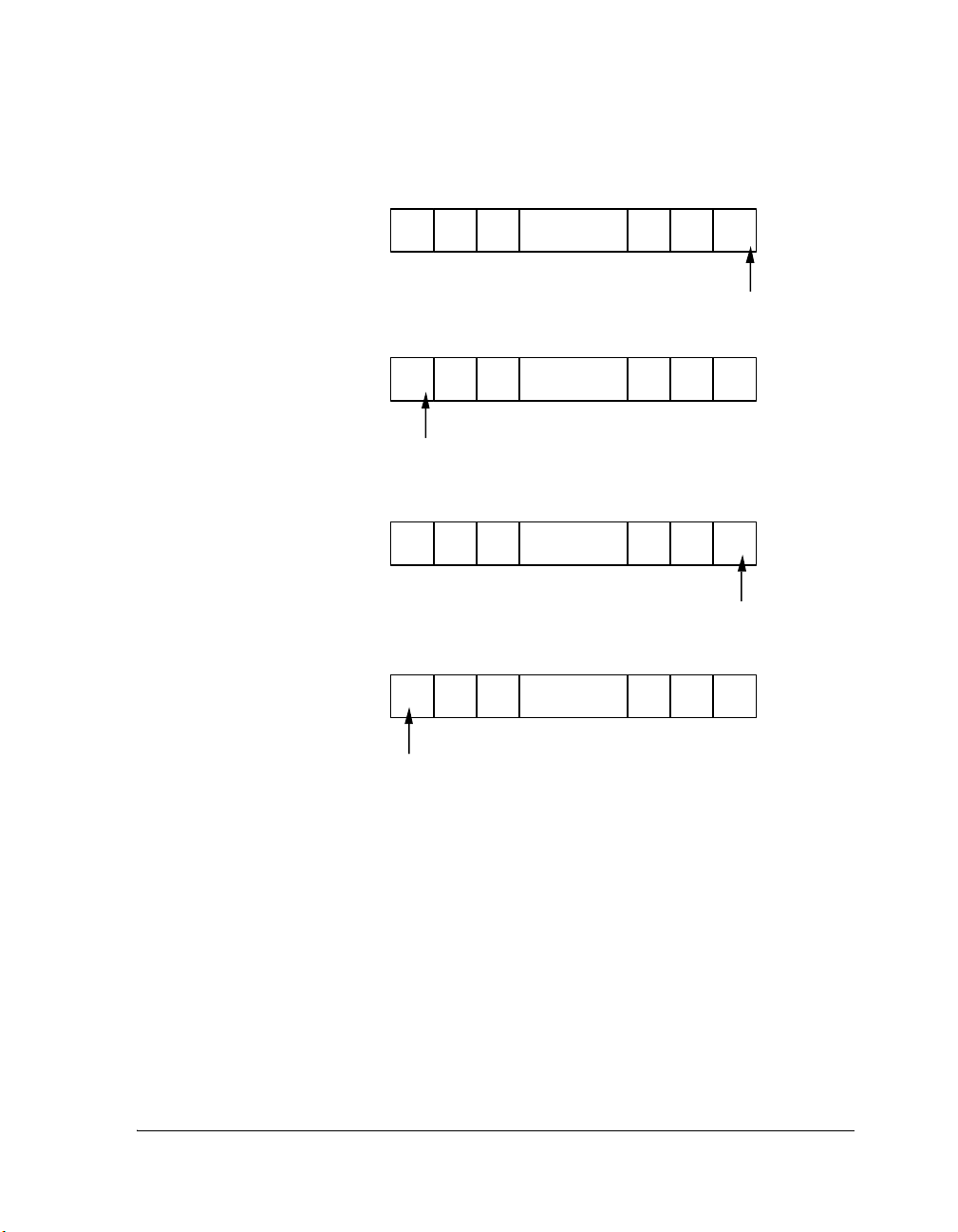
Processing Elements
SIGNED
INTEGER
SIGNED
FRACTIONAL
UNSIGNED
INTEGER
UNSIGNED
FRACTIONAL
31 30 29
BIT
2-22
29
29
-3
WEIGHT
WEIGHT
WEIGHT
-2312302
SIGN
BIT
31 30 29
BIT
-02-12-2
-2
•
SIGN
BIT
BINARY
POINT
BIT 0
31 30 29
2312302
31 30 29 2 1
BIT
-1
.2
•••
•••
•••
•••
21
22212
21
-29
2
21
221
2
-302-312-32
2
-302-31
2
0
0
•
BINARY
POINT
0
0
2
•WEIGHT
BINARY
POINT
0
BINARY POINT
Figure 2-5. 32-Bit Fixed-Point Formats
ADSP-2136x SHARC Processor Programming Reference 2-9
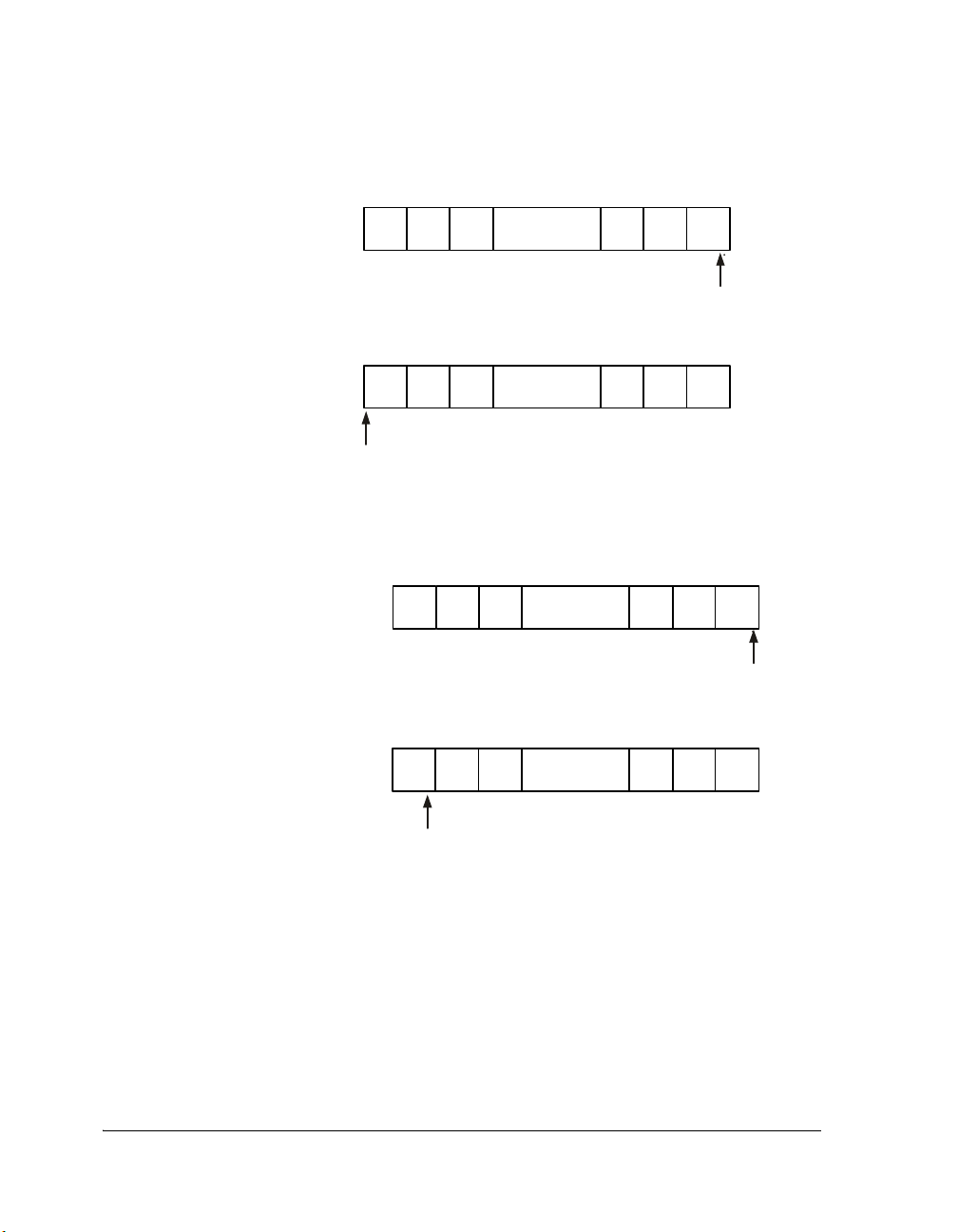
Numeric Formats
63 62 61
UNSIGNED
INTEGER
UNSIGNED
FRACTIONAL
BIT 0
WEIGHT
BIT
WEIGHT
62261
2632
63 62 61 2 1 0
2-22
-3
•
BINARY
POINT
-1
2
•••
••• 2
Figure 2-6. 64-Bit Unsigned Fixed-Point Product
SIGNED INTEGER,
NO LEFT SHIFT
SIGNED FRACTIONAL,
WITH LEFT SHIFT
BIT 0
WEIGHT
BIT 0
WEIGHT
63 62 61
63262261
-2
SIGN
BIT
63 62 61
-202-12
SIGN
BIT
BINARY
POINT
•••
•
-2
•••
21
1
2
2
2
-62
-632-64
2
21
22212
21
-61
2
0
2
•
BINARY
POINT
BINARY
-622-63
2
0
POINT
•
Figure 2-7. 64-Bit Signed Fixed-Point Product
2-10 ADSP-2136x SHARC Processor Programming Reference

Processing Elements
Setting Computational Modes
The MODE1 register controls the operating mode of the processing elements. Table B-2 on page B-5 lists the bits in the MODE1 register. The
following MODE1 bits control computational modes:
• Floating-point data format. Bit 16 (RND32) rounds floating-point
data to 32 bits (if 1) or rounds to 40 bits (if 0).
• Rounding mode. Bit 15 (TRUNC) rounds results with round-to-zero
(if 1) or round-to-nearest (if 0).
• ALU saturation. Bit 13 (ALUSAT) saturates results on positive or
negative fixed-point overflows (if 1) or returns unsaturated results
(if 0).
• Short word sign extension. Bit 14 (SSE) sign extends short word
16-bit data (if 1) or zero-fill the upper 16 bits (if 0).
• Secondary processor element (PEy). Bit 21 (PEYEN) enables com-
putations in PEy (SIMD mode) (if 1) or disables PEy (SISD mode)
(if 0).
ADSP-2136x SHARC Processor Programming Reference 2-11

Setting Computational Modes
32-Bit Floating-Point Format (Normal Word)
In the default mode, (RND32 bit=1), the multiplier and ALU support a single-precision floating-point format, which is specified in the IEEE
754/854 standard. For more information on this standard, see “Numeric
Formats” on page 2-2. This format is IEEE 754/854 compatible for sin-
gle-precision floating-point operations in all respects except:
• The processor does not provide inexact flags. An inexact flag is an
exception flag whose bit position is inexact. The inexact exception
occurs if the rounded result of an operation is not identical to the
exact (infinitely precise) result. Thus, an inexact exception always
occurs when an overflow or an underflow occurs.
• NAN (Not-A-Number) inputs generate an invalid exception and
return a quiet NAN (all 1s).
• Denormal operands, using denormalized (or tiny) numbers, flush
to zero when input to a computational unit and do not generate an
underflow exception. A denormal operand is one of the floating-point operands with an absolute value too small to represent
with full precision in the significant. The denormal exception
occurs if one or more of the operands is a denormal number. This
exception is never regarded as an error.
• The processor supports round-to-nearest and round-toward-zero
modes, but does not support round to +infinity and round to
–infinity.
IEEE single-precision floating-point data uses a 23-bit mantissa with an
8-bit exponent plus sign bit. In this case, the computation unit sets the
eight LSBs of floating-point inputs to zeros before performing the operation. The mantissa of a result rounds to 23 bits (not including the hidden
bit), and the 8 LSBs of the 40-bit result clear to zeros to form a 32-bit
number, which is equivalent to the IEEE standard result.
2-12 ADSP-2136x SHARC Processor Programming Reference

Processing Elements
In fixed-point to floating-point conversion, the rounding boundary is
always 40 bits, even if the
RND32 bit is set.
40-Bit Floating-Point Format
In extended-precision mode (RND32 bit=0), the processor supports a 40-bit
extended-precision floating-point mode, which has eight additional LSBs
of the mantissa and is compliant with the 754/854 standards. However,
results in this format are more precise than the IEEE single-precision standard specifies. Extended-precision floating-point data uses a 31-bit
mantissa with a 8-bit exponent plus sign a bit.
16-Bit Floating-Point Format (Short Word)
The processor supports a 16-bit floating-point storage format and provides instructions that convert the data for 40-bit computations. The
16-bit floating-point format uses an 11-bit mantissa with a 4-bit exponent
plus sign bit. The 16-bit data goes into bits 23 through 8 of a data register.
Two shifter instructions, FPACK and FUNPACK, perform the packing and
unpacking conversions between 32-bit floating-point words and 16-bit
floating-point words. The FPACK instruction converts a 32-bit IEEE floating-point number in a data register into a 16-bit floating-point number.
FUNPACK converts a 16-bit floating-point number in a data register to a
32-bit IEEE floating-point number. Each instruction executes in a single
cycle.
When 16-bit data is written to bits 23 through 8 of a data register, the
processor automatically extends the data into a 32-bit integer (bits 39
through 8). If the
SSE bit in MODE1 is set (1), the processor sign-extends the
upper 16 bits. If the SSE bit is cleared (0), the processor zeros the upper 16
bits.
The 16-bit floating-point format supports gradual underflow. This
method sacrifices precision for dynamic range. When packing a number
that would have underflowed, the exponent clears to zero and the mantissa
ADSP-2136x SHARC Processor Programming Reference 2-13

Setting Computational Modes
(including a “hidden” 1) right-shifts the appropriate amount. The packed
result is a denormal, which can be unpacked into a normal IEEE floating-point number.
32-Bit Fixed-Point Format
The processor represents fixed-point numbers in 32 bits, occupying the 32
MSBs in 40-bit data registers. Fixed-point data may be fractional or integer numbers and unsigned or two’s-complement. Each computational unit
has limitations on how these formats may be mixed for a given operation.
All computational units read the upper 32 bits of data (inputs, operands)
from the 40-bit registers (ignoring the eight LSBs) and write results to the
upper 32 bits (zeroing the eight LSBs).
Rounding Mode
The TRUNC bit in the MODE1 register determines the rounding mode for all
ALU operations, all floating-point multiplies, and fixed-point multiplies
of fractional data. The processor supports two rounding modes—
round-toward-zero and round-toward-nearest. The rounding modes comply with the IEEE 754 standard and have the following definitions:
• Round-toward-zero (TRUNC bit=1). If the result before rounding is
not exactly representable in the destination format, the rounded
result is the number that is nearer to zero. This is equivalent to
truncation.
• Round-toward-nearest (
is not exactly representable in the destination format, the rounded
result is the number that is nearer to the result before rounding. If
the result before rounding is exactly halfway between two numbers
in the destination format (differing by an LSB), the rounded result
is the number that has an LSB equal to zero.
2-14 ADSP-2136x SHARC Processor Programming Reference
TRUNC bit=0). If the result before rounding

Processing Elements
Statistically, rounding up occurs as often as rounding down, so there is no
large sample bias. Because the maximum floating-point value is one LSB
less than the value that represents infinity, a result that is halfway between
the maximum floating-point value and infinity rounds to infinity in this
mode.
Though these rounding modes comply with standards set for floating-point data, they also apply for fixed-point multiplier operations on
fractional data. The same two rounding modes are supported, but only the
round-to-nearest operation is actually performed by the multiplier. Using
its local result register for fixed-point operations, the multiplier
rounds-to-zero by reading only the upper bits of the result and discarding
the lower bits.
Using Computational Status
The multiplier and ALU each provide exception information when executing floating-point operations. Each unit updates overflow, underflow,
and invalid operation flags in the processing element’s arithmetic status
(ASTATx and ASTATy) registers and sticky status (STKYx and STKYy) registers.
An underflow, overflow, or invalid operation from any unit also generates
a maskable interrupt. There are three ways to use floating-point exceptions from computations in program sequencing:
• Enable interrupts and use an interrupt service routine (ISR) to handle the exception condition immediately. This method is
appropriate if it is important to correct all exceptions as they occur.
• Use conditional instructions to test the exception flags in the
ASTATx or ASTATy registers after the instruction executes. This
method permits monitoring each instruction’s outcome.
ADSP-2136x SHARC Processor Programming Reference 2-15

Arithmetic Logic Unit (ALU)
• Use the bit test (
STKY register after a series of operations. If any flags are set, some of
the results are incorrect. Use this method when exception handling
is not critical.
More information on ASTAT and STKY status appears in the sections that
describe the computational units. For summaries relating instructions and
status bits, see Table 2-4, Table 2-5, Table 2-7, Table 2-9, and
Table 2-10.
BTST) instruction to examine exception flags in the
Arithmetic Logic Unit (ALU)
The ALU performs arithmetic operations on fixed-point or floating-point
data and logical operations on fixed-point data. ALU fixed-point instructions operate on 32-bit fixed-point operands and output 32-bit
fixed-point results, and ALU floating-point instructions operate on 32-bit
or 40-bit floating-point operands and output 32-bit or 40-bit floating-point results. ALU instructions include:
• Floating-point addition, subtraction, add/subtract, average
• Fixed-point addition, subtraction, add/subtract, average
• Floating-point manipulation: binary log, scale, mantissa
• Fixed-point add with carry, subtract with borrow, increment,
decrement
• Logical And, Or, Xor, Not
• Functions: ABS, PASS, MIN, MAX, CLIP, COMPARE
• Format conversion
• Reciprocal and reciprocal square root primitives
2-16 ADSP-2136x SHARC Processor Programming Reference

Processing Elements
ALU Operation
ALU instructions take one or two inputs: X input and Y input. These
inputs (known as operands) can be any data registers in the register file.
Most ALU operations return one result; in add/subtract operations, the
ALU operation returns two results; in compare operations, the ALU operation returns no result (only flags are updated). ALU results can be
returned to any location in the register file.
Because of the 5-stage pipeline in the ADSP-2136x processor core, the
operands are fetched before the results are written back. Therefore, the
ALU can read and write the same register file location in a single cycle. If
the ALU operation is fixed-point, the inputs are treated as 32-bit
fixed-point operands. The ALU transfers the upper 32 bits from the
source location in the register file. For fixed-point operations, the result(s)
are 32-bit fixed-point values. Some floating-point operations (LOGB, MANT
and FIX) can also yield fixed-point results.
The processor transfers fixed-point results to the upper 32 bits of the data
register and clears the lower eight bits of the register. The format of
fixed-point operands and results depends on the operation. In most arithmetic operations, there is no need to distinguish between integer and
fractional formats. Fixed-point inputs to operations such as scaling a floating-point value are treated as integers. For purposes of determining status
such as overflow, fixed-point arithmetic operands and results are treated as
two’s-complement numbers.
ALU Saturation
When the ALUSAT bit is set (=1) in the MODE1 register, the ALU is in saturation mode. In this mode, positive fixed-point overflows return the
maximum positive fixed-point number (0x7FFF FFFF), and negative
overflows return the maximum negative number (0x8000 0000).
ADSP-2136x SHARC Processor Programming Reference 2-17

Arithmetic Logic Unit (ALU)
When the
ALUSAT bit is cleared (=0) in the MODE1 register, fixed-point
results that overflow are not saturated; the upper 32 bits of the result are
returned unaltered.
ALU Status Flags
ALU operations update seven status flags in the processing element’s arithmetic status (
the bits in these registers. The following bits in
flag the ALU status (a 1 indicates the condition) of the most recent ALU
operation:
• ALU result zero or floating-point underflow, bit 0 (AZ)
• ALU overflow, bit 1 (AV)
• ALU result negative, bit 2 (AN)
• ALU fixed-point carry, bit 3 (AC)
• ALU X input sign for ABS, MANT operations, bit 4 (AS)
• ALU floating-point invalid operation, bit 5 (AI)
ASTATx and ASTATy) registers. Table B-4 on page B-14 lists
ASTATx or ASTATy registers
• Last ALU operation was a floating-point operation, bit 10 (AF)
• Compare accumulation register results of last eight compare operations, bits 31-24 (
CACC)
ALU operations also update four sticky status flags in the processing element’s sticky status (
lists the bits in these registers. The following bits in
STKYx and STKYy) registers. Table B-5 on page B-20
STKYx or STKYy flag
the ALU status (a 1 indicates the condition). Once set, a sticky flag
remains high until explicitly cleared:
• ALU floating-point underflow, bit 0 (AUS)
• ALU floating-point overflow, bit 1 (
AVS)
2-18 ADSP-2136x SHARC Processor Programming Reference

Processing Elements
• ALU fixed-point overflow, bit 2 (
AOS)
• ALU floating-point invalid operation, bit 5 (AIS)
Flag updates occur at the end of the cycle in which the status is generated
and is available on the next cycle. If a program writes the arithmetic status
register or sticky status register explicitly in the same cycle that the ALU is
performing an operation, the explicit write to the status register supersedes
any flag update from the ALU operation.
ALU Instruction Summary
Table 2-4 and Table 2-5 list the ALU instructions and show how they
relate to ASTATx,y and STKYx,y flags. For more information on assembly
language syntax, see “Instruction Set” in Chapter 8, Instruction Set, and
“Computations Reference” in Chapter 9, Computations Reference. In
these tables, note the meaning of these symbols:
• Rn, Rx, Ry indicate any register file location; treated as fixed-point
• Fn, Fx, Fy indicate any register file location; treated as
floating-point
• * indicates that the flag may be set or cleared, depending on the
results of instruction
• ** indicates that the flag may be set (but not cleared), depending
on the results of the instruction
• – indicates no effect
ADSP-2136x SHARC Processor Programming Reference 2-19

Arithmetic Logic Unit (ALU)
Table 2-4. Fixed-Point ALU Instruction Summary
Instruction ASTATx,y Status Flags STKYx,y Status Flags
Fixed-Point: AZAVANACASAIAFC
Rn = Rx + Ry *** *000–––**–
Rn = Rx – Ry *** *000–––**–
Rn = Rx + Ry + CI * ** *000–––**–
Rn = Rx – Ry + CI – 1 *** *000–––**–
Rn = (Rx + Ry)/2 *0* *000–––––
COMP(Rx, Ry) *0* 0000*––––
COMPU(Rx,Ry) * 0*0000* --------
Rn = Rx + CI * ** *000–––**–
Rn = Rx + CI – 1 * ** *000–––**–
Rn = Rx + 1 *** *000–––**–
Rn = Rx – 1 *** *000–––**–
Rn = –Rx ** ** 000–––**–
Rn = ABS Rx **00* 00–––**–
Rn = PASS Rx *0* 0000–––––
Rn = Rx AND Ry *0* 0000–––––
Rn = Rx OR Ry *0* 0000–––––
Rn = Rx XOR Ry *0* 0000–––––
Rn = NOT Rx *0* 0000–––––
Rn = MIN(Rx, Ry) * 0*0000–––––
Rn = MAX(Rx, Ry) *0*0000–––––
Rn = CLIP Rx BY Ry *0* 0000–––––
A
A
A
A
A
U
V
O
I
C
S
S
S
S
C
2-20 ADSP-2136x SHARC Processor Programming Reference

Processing Elements
Table 2-5. Floating-Point ALU Instruction Summary
Instruction ASTATx,y Status Flags STKYx,y Status Flags
Floating-Point: AZAVANACASAIAFC
Fn = Fx + Fy * * * 0 0 * 1 – ** ** – **
Fn = Fx – Fy * * * 0 0 * 1 – ** ** – **
Fn = ABS (Fx + Fy) * * 0 0 0 * 1 – ** ** – **
Fn = ABS (Fx – Fy) * * 0 0 0 * 1 – ** ** – **
Fn = (Fx + Fy)/2 *0* 00*1–**––**
COMP(Fx, Fy) *0* 00* 1*–––**
Fn = –Fx *** 00*1––**–**
Fn = ABS Fx * *00* *1––**–**
Fn = PASS Fx * 0*00* 1––––**
Fn = RND Fx ** *00* 1––**–**
Fn = SCALB Fx BY Ry * * * 0 0 * 1 – ** ** – **
Rn = MANT Fx * *00* * 1––**–**
Rn = LOGB Fx * ** 00*1––**–**
Rn = FIX Fx BY Ry * * * 0 0 * 1 – ** ** – **
Rn = FIX Fx * * * 0 0 * 1 – ** ** – **
Fn = FLOAT Rx BY Ry ** *0001–****––
Fn = FLOAT Rx *0* 0001–––––
Fn = RECIPS Fx * * * 0 0 * 1 – ** ** – **
Fn = RSQRTS Fx ** *00* 1––**–**
Fn = Fx COPYSIGN Fy *0* 00* 1––––**
Fn = MIN(Fx, Fy) * 0* 00*1––––**
Fn = MAX(Fx, Fy) *0*00* 1––––**
Fn = CLIP Fx BY Fy *0* 00*1––––**
A
A
A
A
A
U
V
O
I
C
S
S
S
S
C
ADSP-2136x SHARC Processor Programming Reference 2-21

Multiply Accumulator (Multiplier)
Multiply Accumulator (Multiplier)
The multiplier performs fixed-point or floating-point multiplication and
fixed-point multiply/accumulate operations. Fixed-point multiply/accumulates are available with cumulative addition or cumulative subtraction.
Multiplier floating-point instructions operate on 32-bit or 40-bit floating-point operands and output 32-bit or 40-bit floating-point results.
Multiplier fixed-point instructions operate on 32-bit fixed-point data and
produce 80-bit results. Inputs are treated as fractional or integer, unsigned
or two’s-complement. Multiplier instructions include:
• Floating-point multiplication
• Fixed-point multiplication
• Fixed-point multiply/accumulate with addition, rounding optional
• Fixed-point multiply/accumulate with subtraction, rounding
optional
• Rounding multiplier result register
• Saturating multiplier result register
• Clearing multiplier result register
Multiplier Operation
The multiplier takes two inputs: X and Y. These inputs (also known as
operands) can be any data registers in the register file. The multiplier can
accumulate fixed-point results in the local multiplier result (MRF) registers
or write results back to the register file. The results in MRF can also be
rounded or saturated in separate operations. Floating-point multiplies
yield floating-point results, which the multiplier writes directly to the register file.
2-22 ADSP-2136x SHARC Processor Programming Reference

Processing Elements
Because of the 5-stage pipeline in the ADSP-2136x processor core, the
operands are fetched before the results are written back. Therefore, the
multiplier can read and write the same register file location in a single
cycle.
For fixed-point multiplies, the multiplier reads the inputs from the upper
32 bits of the data registers. Fixed-point operands may be integer, fractional or both formats. The format of the result matches the format of the
inputs. Each fixed-point operand may be either an unsigned number or a
two’s-complement number. If both inputs are fractional and signed, the
multiplier automatically shifts the result left one bit to remove the redundant sign bit. The register name(s) within the multiplier instruction
specify input data type(s)—Fx for floating-point and Rx for fixed-point.
Multiplier Result Register (Fixed-Point)
Fixed-point operations place 80-bit results in the multiplier’s foreground
MRF register or background MRB register, depending on which is active. For
more information on selecting the result register, see “Alternate (Second-
ary) Data Registers” on page 2-39.
The location of a result in the MRF register’s 80-bit field depends on
whether the result is in fractional or integer format, as shown in
Figure 2-8. If the result is sent directly to a data register, the 32-bit result
with the same format as the input data is transferred, using bits 63-32 for
a fractional result or bits 31-0 for an integer result. The eight LSBs of the
40-bit register file location are zero-filled.
Fractional results can be rounded-to-nearest before being sent to the register file. If rounding is not specified, discarding bits 31-0 effectively
truncates a fractional result (rounds to zero). For more information on
rounding, see “Rounding Mode” on page 2-14.
The MRF register is comprised of the MRF2, MRF1, and MRF0 registers, which
individually can be read from or written to the register file. Each of these
registers has the same format. When data is read from
MRF2, it is
ADSP-2136x SHARC Processor Programming Reference 2-23
Multiply Accumulator (Multiplier)
79 63 31 0
MRF2 MRF0
OVERFLO W UNDERFLOWFRACTIONAL RESULT
OVERFLOW INTEGER RESULTOVERFLOW
MRF1
Figure 2-8. Multiplier Fixed-Point Result Placement
sign-extended to 32 bits as shown in Figure 2-9. The processor zero-fills
the eight LSBs of the 40-bit register file location when data is read from
MRF2, MRF1, or MRF0 written to the register file. When the processor writes
data into MRF2, MRF1, or MRF0 from the 32 MSBs of a register file location,
the eight LSBs are ignored. Data written to MRF1 is sign-extended to MRF2,
repeating the MSB of MRF1 in the 16 bits of MRF2. Data written to MRF0 is
not sign-extended.
16BITS 16 BITS
8BITS
ZEROSSIGN-EXTEND MRF 2
8BITS32BITS
MRF 1
ZEROS
MRF 0
8BITS32 BI TS
ZEROS
Figure 2-9. MR Transfer Formats
2-24 ADSP-2136x SHARC Processor Programming Reference

Processing Elements
In addition to multiply, fixed-point operations include accumulate,
round, and saturate fixed-point data. There are three
MRF register opera-
tions: clear (CLR), round (RND), and saturate (SAT).
The CLR operation (MRF=0) resets the specified MRF register to zero. Often,
it is best to perform this operation at the start of a multiply/accumulate
operation to remove the results of the previous operation.
The RND operation (MRF=RND MRF) applies only to fractional results and
integer results are not effected. This operation rounds the 80-bit MRF value
to nearest at bit 32, for example, the MRF1-MRF0 boundary. Rounding a
fixed-point result occurs as part of a multiply or multiply/accumulate
operation or as an explicit operation on the MRF register. The rounded
result in MRF1 can be sent to the register file or back to the same MRF register. To round a fractional result to zero (truncation) instead of to nearest,
a program transfers the unrounded result from MRF1, discarding the lower
32 bits in MRF0.
The SAT operation (MRF=SAT MRF) sets MRF to a maximum value if the MRF
value has overflowed. Overflow occurs when the MRF value is greater than
the maximum value for the data format—unsigned or two’s-complement
and integer or fractional—as specified in the saturate instruction. The six
possible maximum values appear in Table 2-6. The result from MRF saturation can be sent to the register file or back to the same MRF register.
Table 2-6. Fixed-Point Format Maximum Values (Saturation)
Maximum Number (Hexadecimal)
MRF2 MRF1 MRF0
Two’s-complement fractional (positive) 0000 7FFF FFFF FFFF FFFF
Two’s-complement fractional (negative) FFFF 8000 0000 0000 0000
Two’s-complement integer (positive) 0000 0000 0000 7FFF FFFF
Two’s-complement integer (negative) FFFF FFFF FFFF 8000 0000
ADSP-2136x SHARC Processor Programming Reference 2-25

Multiply Accumulator (Multiplier)
Table 2-6. Fixed-Point Format Maximum Values (Saturation) (Cont’d)
Maximum Number (Hexadecimal)
MRF2 MRF1 MRF0
Unsigned fractional number 0000 FFFF FFFF FFFF FFFF
Unsigned integer number 0000 0000 0000 FFFF FFFF
Multiplier Status Flags
Multiplier operations update four status flags in the processing element’s
arithmetic status registers (ASTATx and ASTATy). “Arithmetic Status Regis-
ters (ASTATx and ASTATy)” on page B-12 lists the bits in these registers.
The bits in the ASTATx or ASTATy registers that indicate the multiplier status (a 1 indicates the condition) of the most recent multiplier operation
are:
• Multiplier result negative, bit 6 (MN)
• Multiplier overflow, bit 7 (MV)
• Multiplier underflow, bit 8 (MU)
• Multiplier floating-point invalid operation, bit 9 (MI)
Multiplier operations also update four “sticky” status flags in the processing element’s sticky status (
STKYx and STKYy) registers. Table B-5 on
page B-20 lists the bits in these registers. Once set, a sticky flag remains
high until explicitly cleared. The bits in the STKYx or STKYy registers that
indicate multiplier status (a 1 indicates the condition) are:
• Multiplier fixed-point overflow, bit 6 (MOS)
• Multiplier floating-point overflow, bit 7 (MVS)
• Multiplier underflow, bit 8 (
• Multiplier floating-point invalid operation, bit 9 (
MUS)
MIS)
2-26 ADSP-2136x SHARC Processor Programming Reference

Processing Elements
Flag updates occur at the end of the cycle in which the status is generated
and are available on the next cycle. If a program writes the arithmetic status register or sticky register explicitly in the same cycle that the multiplier
is performing an operation, the explicit write to
ASTAT or STKY supersedes
any flag update from the multiplier operation.
Multiplier Instruction Summary
Table 2-7 and Table 2-9 list the multiplier instructions and describe how
they relate to ASTATx,y and STKYx,y flags. For more information on
assembly language syntax, see “Instruction Set” in Chapter 8, Instruction
Set, and “Computations Reference” in Chapter 9, Computations Reference. In these tables, note the meaning of the following symbols:
• Rn, Rx, Ry indicate any register file location; treated as fixed-point
• Fn, Fx, Fy indicate any register file location; treated as
floating-point
• * indicates that the flag may be set or cleared, depending on results
of instruction
• ** indicates that the flag may be set (but not cleared), depending
on results of instruction
• – indicates no effect
• The Input Mods column indicates the types of optional modifiers
that can be applied to the instruction inputs. For a list of modifiers,
see Table 2-8.
ADSP-2136x SHARC Processor Programming Reference 2-27

Multiply Accumulator (Multiplier)
Table 2-7. Fixed-Point Multiplier Instruction Summary
Instruction
Fixed-Point:
For Input Mods, see
Table 2-8
Rn = Rx * Ry 1 * * * 0 – ** – –
MRF = Rx * Ry 1 ***0–**––
MRB = Rx * Ry 1 ***0–**––
Rn = MRF + Rx * Ry 1 * * * 0 – ** – –
Rn = MRB + Rx * Ry 1 * * * 0 – ** – –
MRF = MRF + Rx * Ry 1 * * * 0 – ** – –
MRB = MRB + Rx * Ry 1 * * * 0 – ** – –
Rn = MRF – Rx * Ry 1 * * * 0 – ** – –
Rn = MRB – Rx * Ry 1 * * * 0 – ** – –
MRF = MRF – Rx * Ry 1 * * * 0 – ** – –
MRB = MRB – Rx * Ry 1 * * * 0 – ** – –
Rn = SAT MRF 2 * * * 0 – ** – –
Rn = SAT MRB 2 * * * 0 – ** – –
MRF = SAT MRF 2 * * * 0 – ** – –
MRB = SAT MRB 2 * * * 0 – ** – –
Rn = RND MRF 3 * * * 0 – ** – –
Rn = RND MRB 3 * * * 0 – ** – –
MRF = RND MRF 3 * * * 0 – ** – –
MRB = RND MRB 3 * * * 0 – ** – –
MRF = 0 – 0000––––
MRB = 0 – 0000––––
MRxF = Rn – 0000––––
MRxB = Rn – 0000––––
Rn = MRxF – 0000––––
Rn = MRxB – 0000––––
Input
Mods
ASTATx,y Flags STKYx,y Flags
M
M
M
MNM
U
M
U
O
V
I
S
S
M
V
S
M
I
S
2-28 ADSP-2136x SHARC Processor Programming Reference

Processing Elements
Table 2-8. Input Modifiers for Fixed-Point Multiplier Instruction
Input
Mods
from
Table
2-7
1 (SSF), (SSI), (SSFR), (SUF), (SUI), (SUFR), (USF), (USI), (USFR), (UUF), (UUI), or
2 (SF), (SI), (UF), or (UI)
3 (SF) or (UF)
Input Mods—Options For Fixed-Point Multiplier Instructions
Note the meaning of the following symbols in this table:
Signed input — S
Unsigned input — U
Integer input — I
Fractional input — F
Fractional inputs, Rounded output — FR
Note that (SF) is the default format for one-input operations, and (SSF) is the
default format for two-input operations.
(UUFR)
Table 2-9. Floating-Point Multiplier Instruction Summary
Instruction ASTATx,y Flags STKYx,y Flags
Floating-Point: M
Fn = Fx * Fy ******–****
M
MVM
U
N
M
M
M
M
I
U
O
V
I
S
S
S
S
ADSP-2136x SHARC Processor Programming Reference 2-29

Barrel Shifter (Shifter)
Barrel Shifter (Shifter)
The shifter performs bit-wise operations on 32-bit fixed-point operands.
Shifter operations include:
• Shifts and rotates from off-scale left to off-scale right
• Bit manipulation operations, including bit set, clear, toggle, and
test
• Bit field manipulation operations, including extract and deposit
• Fixed-point/floating-point conversion operations, including exponent extract, number of leading 1s or 0s
Shifter Operation
The shifter takes one to three inputs: X, Y, and Z. The inputs (known as
operands) can be any register in the register file. Within a shifter instruction, the inputs serve as follows.
• The X input provides data that is operated on.
• The Y input specifies shift magnitudes, bit field lengths, or bit
positions.
• The Z input provides data that is operated on and updated.
In the following example,
Z input. The shifter returns one output (Rn) to the register file.
Rn = Rn OR LSHIFT Rx BY Ry;
As shown in Figure 2-10, the shifter fetches input operands from the
upper 32 bits of a register file location (bits 39-8) or from an immediate
value in the instruction. Because of the 5-stage pipeline in the
2-30 ADSP-2136x SHARC Processor Programming Reference
Rx is the X input, Ry is the Y input, and Rn is the

Processing Elements
ADSP-2136x processor core, the operands are fetched before the results
are written back. Therefore, the shifter can read and write the same register file location in a single cycle.
The X input and Z input are always 32-bit fixed-point values. The Y input
is a 32-bit fixed-point value or an 8-bit field (shf8), positioned in the register file. These inputs appear in Figure 2-10.
Some shifter operations produce 8 or 6-bit results. As shown in
Figure 2-11, the shifter places these results in the shf8 field or the bit6
field and sign-extends the results to 32 bits. The shifter always returns a
32-bit result.
39 70
32-BIT Y INPUT OR RESULT
39 15 7 0
SHF8
8-BIT Y INPUT OR RESULT
Figure 2-10. Register File Fields for Shifter Instructions
The shifter supports bit field deposit and bit field extract instructions for
manipulating groups of bits within an input. The Y input for bit field
instructions specifies two 6-bit values, bit6 and len6, which are positioned
in the Ry register as shown in Figure 2-11. The shifter interprets bit6 and
len6 as positive integers. Bit6 is the starting bit position for the deposit or
extract, and len6 is the bit field length, which specifies how many bits are
deposited or extracted.
ADSP-2136x SHARC Processor Programming Reference 2-31

Barrel Shifter (Shifter)
39322
41680
39 19 13 7
LEN6
12-BIT Y INPUT
BIT6
Figure 2-11. Register File Fields for FDEP, FEXT Instructions
Field deposit (
FDEP) instructions take a group of bits from the input regis-
ter (starting at the LSB of the 32-bit integer field) and deposit the bits as
directed anywhere within the result register. The bit6 value specifies the
starting bit position for the deposit. Figure 2-13 shows how the inputs,
bit6 and len6, work in a field deposit instruction
Rn = FDEP Rx By Ry
Figure 2-12 shows bit placement for the following field deposit
instruction:
R0 = FDEP R1 By R2;
R2
00000000
00000000 00000000
00000010
00010000
len6 bi t6
len6 = 8
bit6 = 16
0x0000 0210 00
0
39 32 16
R1
R0
00000000
39 32 24 16 8 0
00000000
00000000 00000000 00000000
11111111
24
16
00000000 00000000 00000000
16 8 0
STARTING BIT POSITION
FOR DEPOSIT
8
11111111
8
0
REFERENCE POINT
0
0x0000 00FF 00
0x00FF 0000 00
Figure 2-12. Bit Field Deposit Instruction
2-32 ADSP-2136x SHARC Processor Programming Reference

Processing Elements
39 19 13 7
RY
RY DETERMINES LENGTH OF BIT FIELD TO TAKE FROM RX AND STARTING POSITION
39 7
RX
LEN6 = NUMBER OF BITS TO TAKE FROM RX, STARTING FROM LSB OF 32-BIT FIELD
39 7
RN
BIT6 = STARTING BIT POSITIONFOR DEPOSIT, REFERENCEDFROM LSB OF 32-BIT FIELD
DEPOSIT FIELD
BIT6 REFERENCE POINT
LEN6
FOR DEPOSIT IN RN
BIT6
Figure 2-13. Bit Field Deposit Instruction
Field extract (
FEXT) instructions extract a group of bits as directed from
anywhere within the input register and place them in the result register,
aligned with the LSB of the 32-bit integer field. The bit6 value specifies
the starting bit position for the extract.
0
0
0
Figure 2-14 shows bit placement for the following field extract
instruction:
R3 = FEXT R4 By R5;
ADSP-2136x SHARC Processor Programming Reference 2-33

Barrel Shifter (Shifter)
39 32 24 16 8 0
R5
00000000
00000000 00000000
00000010
00010111
0x0000 0217 00
len6 bit6
39 32 24 16 8 0
R4
R3
10000111
39 32 24 16 8 0
00000000 000 00000
10000000
STARTING BIT POSITION
FOR DEPOSIT
00000000 00000000 00000000
1680
00000000
16 8 0
00001111
len6 = 8
bit6 = 23
REFERENCE POINT
00000000
0x8710 0000 00
0x0000 000F 00
Figure 2-14. Bit Field Extract Instruction
Shifter Status Flags
Shifter operations update three status flags in the processing element’s
arithmetic status registers (ASTATx and ASTATy). Table B-4 on page B-14
lists the bits in these registers. The following bits in the ASTATx or ASTATy
registers indicate shifter status (a 1 indicates the condition) for the most
recent ALU operation:
• Shifter overflow of bits to left of MSB, bit 11 (SV)
• Shifter result zero, bit 12 (
SZ)
• Shifter input sign for exponent extract only, bit 13 (SS)
A flag update occurs at the end of the cycle in which the status is generated and is available on the next cycle. If a program writes the arithmetic
status register explicitly in the same cycle that the shifter is performing an
operation, the explicit write to ASTAT supersedes any flag update caused by
the shift operation.
2-34 ADSP-2136x SHARC Processor Programming Reference

Processing Elements
Shifter Instruction Summary
Table 2-10 lists the shifter instructions and shows how they relate to
ASTATx,y flags. For more information on assembly language syntax, see
“Instruction Set” in Chapter 8, Instruction Set, and “Computations Reference” in Chapter 9, Computations Reference. In these tables, note the
meaning of the following symbols:
• The Rn, Rx, Ry operands indicate any register file location; bit fields
used depend on instruction
• The Fn, Fx operands indicate any register file location; floating-point word
• The * symbol indicates that the flag may be set or cleared, depending on data
Table 2-10. Shifter Instruction Summary
Instruction ASTATx,y Flags
SZ SV SS
Rn = LSHIFT Rx BY Ry * * 0
Rn = LSHIFT Rx BY <data8> * * 0
Rn = Rn OR LSHIFT Rx BY Ry * * 0
Rn = Rn OR LSHIFT Rx BY <data8> * * 0
Rn = ASHIFT Rx BY Ry * * 0
Rn = ASHIFT Rx BY<data8> * * 0
Rn = Rn OR ASHIFT Rx BY Ry * * 0
Rn = Rn OR ASHIFT Rx BY <data8> * * 0
Rn = ROT Rx BY Ry * 0 0
Rn = ROT Rx BY <data8> * 0 0
Rn = BCLR Rx BY Ry * * 0
Rn = BCLR Rx BY <data8> * * 0
Rn = BSET Rx BY Ry * * 0
ADSP-2136x SHARC Processor Programming Reference 2-35

Barrel Shifter (Shifter)
Table 2-10. Shifter Instruction Summary (Cont’d)
Instruction ASTATx,y Flags
SZ SV SS
Rn = BSET Rx BY <data8> * * 0
Rn = BTGL Rx BY Ry * * 0
Rn = BTGL Rx BY <data8> * * 0
BTST Rx BY Ry * * 0
BTST Rx BY <data8> * * 0
Rn = FDEP Rx BY Ry * * 0
Rn = FDEP Rx BY <bit6>:<len6> * * 0
Rn = Rn OR FDEP Rx BY Ry * * 0
Rn = Rn OR FDEP Rx BY <bit6>:<len6> * * 0
Rn = FDEP Rx BY Ry (SE) * * 0
Rn = FDEP Rx BY <bit6>:<len6> (SE) * * 0
Rn = Rn OR FDEP Rx BY Ry (SE) * * 0
Rn = Rn OR FDEP Rx BY <bit6>:<len6> (SE) * * 0
Rn = FEXT Rx BY Ry * * 0
Rn = FEXT Rx BY <bit6>:<len6> * * 0
Rn = FEXT Rx BY Ry (SE) * * 0
Rn = FEXT Rx BY <bit6>:<len6> (SE) * * 0
Rn = EXP Rx (EX) * 0 *
Rn = EXP Rx * 0 *
Rn = LEFTZ Rx * * 0
Rn = LEFTO Rx * * 0
Rn = FPACK Fx 0 * 0
Fn = FUNPACK Rx 0 0 0
2-36 ADSP-2136x SHARC Processor Programming Reference

Processing Elements
Data Register File
Each of the processor’s processing elements has a data register file, which
is a set of data registers that transfers data between the data buses and the
computational units. These registers also provide local storage for operands and results.
The two register files consist of 16 primary registers and 16 alternate (secondary) registers. The data registers are 40 bits wide. Within these
registers, 32-bit data is left-justified. If an operation specifies a 32-bit data
transfer to these 40-bit registers, the eight LSBs are ignored on register
reads, and the LSBs are cleared to zeros on writes.
Program memory data accesses and data memory accesses to and from the
register file(s) occur on the PM data bus and DM data bus, respectively.
One PM data bus access for each processing element and/or one DM data
bus access for each processing element can occur in one cycle. Transfers
between the register files and the DM or PM data buses can move up to
64 bits of valid data on each bus.
If an operation specifies the same register file location as both an input
and output, the 5-stage pipeline fetches the operands before the results are
written back. Therefore, the processor uses the old data as the operand,
before updating the location with the new result data. If writes to the same
location take place in the same cycle, only the write with higher precedence actually occurs. The processor determines precedence for the write
operation from the source of the data; from highest to lowest, the precedence is:
1. Data memory or universal register (
2. Program memory
3. PEx ALU
ADSP-2136x SHARC Processor Programming Reference 2-37
Ureg)

Data Register File
4. PEy ALU
5. PEx Multiplier
6. PEy Multiplier
7. PEx Shifter
8. PEy Shifter
The data register file in Figure 2-1 on page 2-3 lists register names of
R0
through R15 within the PEx’s register file. When a program refers to these
registers as R0 through R15, the computational units treat the contents of
these registers as fixed-point data. To perform floating-point computations, refer to these registers as F0 through F15. For example, the following
instructions refer to the same registers, but direct the computational units
to perform different operations:
F0 = F1 * F2; /* floating-point multiply */
R0 = R1 * R2; /* fixed-point multiply */
The F and R prefixes on register names do not effect the 32-bit or 40-bit
data transfer; the naming convention only determines how the ALU, multiplier, and shifter treat the data.
To maintain compatibility with code written for previous SHARC processors, the assembly syntax accommodates references to the PEx and PEy
data registers.
Code may refer only to the PEy data registers (
S0 through S15) for data
move instructions. The rules for using register names are:
•
R0 through R15 and F0 through F15 refer to PEx registers for data
move and computational instructions, whether the processor is in
SISD or SIMD mode.
2-38 ADSP-2136x SHARC Processor Programming Reference

Processing Elements
•
R0 through R15 and F0 through F15 refer to both PEx and PEy reg-
ister for computational instructions in SIMD mode.
• S0 through S15 refer to PEy registers for data move instructions,
when the processor is in SISD or SIMD mode.
For more information on SISD and SIMD computational operations, see
“Secondary Processing Element (PEy)” on page 2-45. For more informa-
tion on ADSP-2136x assembly language, see“Instruction Set” in
Chapter 8, Instruction Set, and “Computations Reference” in Chapter 9,
Computations Reference.
Alternate (Secondary) Data Registers
Each register file has an alternate register set. To facilitate fast context
switching, the processor includes alternate register sets for data, results,
and data address generator registers. Bits in the MODE1 register control
when alternate registers become accessible. While inaccessible, the contents of alternate registers are not affected by processor operations. Note
that there is a one cycle latency from the time when writes are made to the
MODE1 register until an alternate register set can be accessed. The alternate
register sets for data and results are described in this section. For more
information on alternate data address generator registers, see “Alternate
(Secondary) DAG Registers” on page 4-6.
Bits in the
sets: the lower half (
S8-S15). To share data between contexts, a program places the data to be
MODE1 register can activate independent alternate data register
R0-R7 and S0-S7) and the upper half (R8-R15 and
shared in one half of either the current processing element’s register file or
the opposite processing element’s register file and activates the alternate
register set of the other half. For information on how to activate alternate
data registers, see the description of the
MODE1 register below.
ADSP-2136x SHARC Processor Programming Reference 2-39

Alternate (Secondary) Data Registers
Each multiplier has a primary or foreground (
MRF) register and alternate or
background (MRB) results register. A bit in the MODE1 register selects which
result register receives the result from the multiplier operation, swapping
which register is the current MRF or MRB. This swapping facilitates context
switching. Unlike other registers that have alternates, both MRF and MRB are
accessible at the same time. Fixed-point multiplies can accumulate results
in the MRF or MRB registers, without regard to the state of the MODE1 register. With this arrangement, code can use the result registers as primary
and alternate accumulators, or code can use these registers as two parallel
accumulators. This feature facilitates complex math.
The MODE1 register controls the access to alternate registers. Table B-2 on
page B-5 lists the bits in MODE1. The following bits in the MODE1 register
control alternate registers (a 1 enables the alternate set):
• Secondary registers for computational unit results, bit 2 (SRCU)
• Secondary registers for the hi register file, R8–R15 and S8–S15, bit 7
(SRRFH)
• Secondary registers for the lo register file, R0–R7 and S0–S7, bit 10
(SRRFL)
The following example demonstrates how code should handle the one
cycle of latency—from the instruction that sets the bit in the MODE1 register until the alternate registers may be accessed. Note that it is possible to
use any instruction that does not access the switching register file instead
of a NOP instruction.
BIT SET MODE1 SRRFL; /* activate alternate reg. file */
NOP; /* wait for access to alternates */
R0 = 7;
2-40 ADSP-2136x SHARC Processor Programming Reference

Processing Elements
Multifunction Computations
The processor supports multiple parallel (multifunction) computations by
using the parallel data paths within its computational units. These instructions complete in a single cycle, and they combine parallel operation of
the multiplier and the ALU or dual ALU functions. The multiple operations perform as if they were in corresponding single function
computations. Multifunction computations also handle flags in the same
way as the single function computations, except that in the dual add/subtract computation, the ALU flags from the two operations are ORed
together.
To work with the available data paths, the computational units constrain
which data registers hold the four input operands for multifunction computations. These constraints limit which registers may hold the X input
and Y input for the ALU and multiplier.
Figure 2-15 shows a computational unit and indicates which registers may
serve as X inputs and Y inputs for the ALU and multiplier. For example,
the X input to the ALU can only be R8, R9, R10 or R11. Note that the
shifter is gray in Figure 2-15 to indicate no shifter multifunction
operations.
Table 2-12, Table 2-13, Table 2-14, and Table 2-15 list the multifunc-
tion computations. For more information on assembly language syntax,
see“Instruction Set” in Chapter 8, Instruction Set, and“Computations
Reference” in Chapter 9, Computations Reference. Table 2-11 provides
the description of the following symbols.
ADSP-2136x SHARC Processor Programming Reference 2-41

Multifunction Computations
MODE1
XY ZXY XY
MULTIPLIER SHIFTER ALU
TO PROGRAM SEQUENCER
PM DATA BUS
DM DATA BUS
REGISTER FILE
(16 x 40-BIT)
R0
R1
R2
R3
R4
R5
R6
R7
MRF2 MRF0MRF1
ASTATX STKYX
R8
R9
R10
R11
R12
R13
R14
R15
NOTE THAT SHIFTER IS FADED
HERE, INDICATING THAT IT IS
NOTAVAILABLE FOR
MULTIFUNCTION INSTRUCTIONS.
Figure 2-15. Input Registers for Multifunction Computations
(ALU and Multiplier)
2-42 ADSP-2136x SHARC Processor Programming Reference

Processing Elements
Table 2-11. Multifunction Computation Symbol Descriptions
Symbol Description
Rm, Ra, Rs, Rx, Ry any register file location; fixed-point
Fm, Fa, Fs, Fx, Fy any register file location; floating-point
R3–0 data file registers R3, R2, R1, or R0
R7-4 data file registers R7, R6, R5 or R4
F3–0 data file registers F3, F2, F1, or F0
F7–4 data file registers F7, F6, F5, or F4
R11–8 data file registers R11, R10, R9, or R8
F11–8 data file registers F11, F10, F9, or F8
R15–12 data file registers R15, R14, R13, or R12
F15–12 data file registers F15, F14, F13, or F12
SSFR the X input is signed, the Y input is signed, use fractional inputs,
and rounded-to-nearest output
SSF the X input is signed, Y input is signed, use fractional input
Table 2-12. Dual Add and Subtract
Ra = Rx + Ry, Rs = Rx – Ry
Fa = Fx + Fy, Fs = Fx – Fy
Table 2-13. Fixed-Point Multiply and Add, Subtract, or Average
(Any combination of left and right column)
Rm = R3-0 * R7-4 (SSFR), Ra = R11-8 + R15-12
MRF = MRF + R3-0 * R7-4 (SSF), Ra = R11-8 – R15-12
Rm = MRF + R3-0 * R7-4 (SSFR), Ra = (R11-8 + R15-12)/2
MRF = MRF – R3-0 * R7-4 (SSF),
Rm = MRF – R3-0 * R7-4 (SSFR),
ADSP-2136x SHARC Processor Programming Reference 2-43

Multifunction Computations
Table 2-14. Floating-Point Multiply and ALU Operation
Fm = F3-0 * F7-4, Fa = F11-8 + F15-12
Fm = F3-0 * F7-4, Fa = F11-8 – F15-12
Fm = F3-0 * F7-4, Fa = FLOAT R11-8 by R15-12
Fm = F3-0 * F7-4, Ra = FIX F11-8 by R15-12
Fm = F3-0 * F7-4, Fa = (F11-8 + F15-12)/2
Fm = F3-0 * F7-4, Fa = ABS F11-8
Fm = F3-0 * F7-4, Fa = MAX (F11-8, F15-12)
Fm = F3-0 * F7-4, Fa = MIN (F11-8, F15-12)
Table 2-15. Multiply With Dual Add and Subtract
Rm = R3-0 * R7-4 (SSFR), Ra = R11-8 + R15-12, Rs = R11-8 – R15-12
Fm = F3-0 * F7-4, Fa = F11-8 + F15-12, Fs = F11-8 – F15-12
Another type of multifunction operation available on the processor combines transfers between the results and data registers and transfers between
memory and data registers. These parallel operations complete in a single
cycle. For example, the processor can perform the following multiply and
parallel read of data memory:
MRF = MRF – R5 * R0, R6 = DM(I1,M2);
Or, the processor can perform the following result register transfer and
parallel read:
R5 = MR1F, R6 = DM(I1,M2);
2-44 ADSP-2136x SHARC Processor Programming Reference

Processing Elements
Secondary Processing Element (PEy)
The ADSP-2136x processor contains two sets of computational units and
associated register files. As shown in Figure 2-16, these two processing elements (PEx and PEy) support SIMD operation.
DIFFERENT DATA GOES TO EACH ELEMENT
16/32/40/64
16/32/40/64
PROGRAM
SEQUENCER
BARREL
SHIFTER
ALU
DATA
REGISTER
FILE
(PEy)
16 x 40-BIT
MULT
BUS
CONNECT
(PX)
MULT
PM DATA BUS
DM DATA BUS
DATA
REGISTER
FILE
(PEx)
16 x 40-BIT
BARREL
SHIFTER
ALU
SAME INSTRUCTION GOES TO BOTH ELEMENTS
Figure 2-16. Block Diagram Showing Secondary Execution Complex
MODE1 register controls the operating mode of the processing ele-
The
ments. Table B-2 on page B-5 lists the bits in MODE1. The PEYEN bit (bit
21) in the
When
MODE1 register enables or disables the PEy processing element.
PEYEN is cleared (0), the ADSP-2136x processor operates in SISD
mode, using only PEx. When the PEYEN bit is set (1), the processor operates in SIMD mode, using the PEx and PEy processing elements. There is
a one cycle delay after PEYEN is set or cleared, before the change to or from
SIMD mode takes effect.
ADSP-2136x SHARC Processor Programming Reference 2-45

Secondary Processing Element (PEy)
To support SIMD, the processor performs these parallel operations:
• Dispatches a single instruction to both processing element’s computational units
• Loads two sets of data from memory, one for each processing
element
• Executes the same instruction simultaneously in both processing
elements
• Stores data results from the dual executions to memory
L
The two processing elements are symmetrical; each contains these functional blocks:
Using the information here and in“Instruction Set” in Chapter 8,
Instruction Set, and “Computations Reference” in Chapter 9,
Computations Reference. It is possible through the SIMD mode’s
parallelism to double performance over similar algorithms running
in SISD (ADSP-2106x processor compatible) mode.
•ALU
• Multiplier primary and alternate result registers
• Shifter
• Data register file and alternate register file
Dual Compute Units Sets
The computational units (ALU, multiplier, and shifter) in PEx and PEy
are identical. The data bus connections for the dual computational units
permit asymmetric data moves to, from, and between the two processing
elements. Identical instructions execute on the PEx and PEy computational units; the difference is the data. The data registers for PEy
operations are identified (implicitly) from the PEx registers in the
2-46 ADSP-2136x SHARC Processor Programming Reference
 Loading...