ANALOG DEVICES ADSP-21161N Service Manual

Engineer To Engineer Note EE-163
a
Technical Notes on using Analog Devices' DSP components and development tools
Contact our technical support by phone: (800) ANALOG-D or e-mail: dsp.support@analog.com
Or vi sit ou r on-l ine re sourc es ht tp:// www.analog.com/dsp and http://www.analog.com/dsp/EZAnswers
The ADSP-21161 SHARC® On-chip SDRAM Controller
Contributed by R.Hoffmann September 25, 2003
Introduction
If you use a DSP to address SDRAM, you will need additional hardware or software to handle the
multiplexed row and column addressing and the refresh and pre-charge requirements. The ADSP-21161N
SHARC® DSP uses a hardware intensive solution, an on-chip SDRAM controller.
The application note introduces the On-chip SDRAM controller‘s characteristics. Basically, the internal
signal chain is shown with the necessary address-mapping scheme. The command truth table gives
detailed information about execution in the SDRAM. The important power up sequence summarizes deep
information to start successful designs. Code execution is described to get optimized performance. A
timing overview demonstrates the performance for different access modes. Refer also to “[4] ABC of
SDRAMs (EE-126)”
Content
Introduction ...............................................................................................................................................................................1
Content .......................................................................................................................................................................................1
1 – Signal Chain of SDRAM.....................................................................................................................................................4
2 – On-Chip Controller Architecture ......................................................................................................................................4
2.1 – Command Logic.................................................................................................................................................................4
2.2 – SHARC Address Buffer ..................................................................................................... ................................................5
2.3 – Address Multiplexer ...........................................................................................................................................................5
2.4 – Data Buffer.........................................................................................................................................................................5
2.5 – Clock Divider .....................................................................................................................................................................5
2.6 – I/O Capability.....................................................................................................................................................................5
2.7 – SDRAM Types...................................................................................................................................................................5
2.8 – Control Registers................................................................................................................................................................6
3 – Command Coding................................................................................................................................................................6
3.1 - Pin Description of Controller..............................................................................................................................................6
3.2 - Controller Command Truth Table.......................................................................................................................................6
3.3 – Relevant Specs....................................................................................................................................................................7
3.4 - Simplified State Diagram....................................................................................................................................................7
3.5 – Setup and Hold Times ........................................................................................................................................................7
4 – Hardware Properties...........................................................................................................................................................9
Copyright 2003, Analog Devices, Inc. All rights reserved. Analog Devices assumes no responsibility for customer product design or the use or application of
customers’ products or for any infringements of patents or rights of others which may result from Analog Devices assistance. All trademarks and logos are property
of their respective holders. Information furnished by Analog Devices Applications and Development Tools Engineers is believed to be accurate and reliable, however
no responsibility is assumed by Analog Devices regarding technical accuracy and topicality of the content provided in Analog Devices’ Engineer-to-Engineer Notes.

a
4.1 – SDRAM Interface Speed Control.......................................................................................................................................9
4.2 – SDRAM Clock Control ......................................................................................................................................................9
4.3 – SDRAM Address Space ...................................................................................................................................................10
4.4 – Address Mapping Scheme................................................................................................................................................10
4.5 – SDRAM Transfer Interruption .........................................................................................................................................11
4.6 – Interface during Reset.......................................................................................................................................................11
4.7 – Extended Precision...........................................................................................................................................................11
4.8 – Circular Access.................................................................................................................................................................12
5 – Command Properties ........................................................................................................................................................12
5.1 – Mode Register Set (MRS) ................................................................................................................................................12
5.2 – Deselect (DESL)...............................................................................................................................................................12
5.3 – I/O Mask Function (DQM)...............................................................................................................................................12
5.4 – SDRAM Bank Select........................................................................................................................................................13
5.5 – SDRAM Address 10 (SDA 10)........................................................................................................................................13
5.6 – Write (WR).......................................................................................................................................................................13
5.7 – Read (RD).........................................................................................................................................................................14
5.8 – Precharge All (PREA) ......................................................................................................................................................14
5.9 – Auto Refresh (REF) ..........................................................................................................................................................14
5.10 – Self Refresh (SREF).......................................................................................................................................................14
6 – Shared Memory .................................................................................................................................................................14
6.1 – MRS..................................................................................................................................................................................14
6.2 – REF...................................................................................................................................................................................15
6.3 – SREF.................................................................................................................................................................................15
6.4 – PREA................................................................................................................................................................................15
7 – Programming the SDRAM Interface...............................................................................................................................15
7.1 – Guideline ..........................................................................................................................................................................15
7.2 – Wait Register (Wait States) ..............................................................................................................................................15
7.3 – Refresh Counter (SDRDIV) .............................................................................................................................................15
7.4 – SDRAM Controller (SDCTL) ..........................................................................................................................................16
7.5 – SDRAM (SDCTL)............................................................................................................................................................17
7.6 – Reprogramming................................................................................................................................................................17
8– Timing Power up Sequence................................................................................................................................................18
8.1– Hardware ...........................................................................................................................................................................18
8.2 – Controller..........................................................................................................................................................................18
8.3 – SDRAM............................................................................................................................................................................19
8.4 – External Buffering Access................................................................................................................................................19
8.5 – Host Access ......................................................................................................................................................................19
9 – DMA Transfers..................................................................................................................................................................20
9.1 – Internal Memory and SDRAM.........................................................................................................................................20
9.2 – Host and SDRAM.............................................................................................................................................................21
10 – Examples ADSP-21161N EZ-KIT Lite..........................................................................................................................21
10.1 – Jumper Settings...............................................................................................................................................................21
10.2 – Configuration 1...............................................................................................................................................................21
10.3 – Configuration 2...............................................................................................................................................................22
11 – Code Execution from SDRAM.......................................................................................................................................23
11.1 – Hardware ........................................................................................................................................................................23
11.2 – Simulator/Loader............................................................................................................................................................24
11.3 – Emulator .........................................................................................................................................................................24
The ADSP-21161 SHARC® On-chip SDRAM Controller (EE-163) Page 2 of 50

a
11.4 – Packing Effects...............................................................................................................................................................25
11.5 – Instruction Pipeline.........................................................................................................................................................27
11.6 – Sequential Code crossing Page/Bank .............................................................................................................................29
11.7 – Non Sequential Code same Page/Bank...........................................................................................................................29
11.8 – Non Sequential Code different Page/Bank.....................................................................................................................29
12 – Loop Execution from SDRAM.......................................................................................................................................29
12.1 – Single Loop with DM Data Access ................................................................................................................................29
12.2 – Single Loop with PM Data Access, Cache enabled........................................................................................................29
12.3 – Single Loop with PM Data Access, Cache disabled.......................................................................................................30
12.4 – Code Execution Performance Overview.........................................................................................................................31
13 – Optimizing the Performance ..........................................................................................................................................32
13.1 – SDRAMs for Data Storage.............................................................................................................................................32
13.2 – SDRAMs for Code Storage............................................................................................................................................33
13.3 – External Buffering..........................................................................................................................................................33
13.4 – SDRAM PC Modules.....................................................................................................................................................34
13.5 – Rules for Optimized Performance..................................................................................................................................34
14 – SDRAM and Booting.......................................................................................................................................................35
14.1 – Loader Kernel.................................................................................................................................................................35
14.2 – Booting Modes ...............................................................................................................................................................35
14.3 – In Circuit Emulation (ICE).............................................................................................................................................36
15 – Core and DMA Transfers to SDRAM...........................................................................................................................36
15.1 – Sequential Reads without Interruption ...........................................................................................................................37
15.2 – Sequential Reads with minimum Interruption................................................................................................................38
15.3 – Non Sequential Reads without Interruption ...................................................................................................................39
15.4 – Sequential Writes without Interruption ..........................................................................................................................40
15.5 – Sequential Writes with minimum Interruption...............................................................................................................41
15.6 – Non Sequential Writes without Interruption...................................................................................................................42
15.7 – Minimum Write to Read Interval....................................................................................................................................43
15.8 – Minimum Read to Write Interval....................................................................................................................................44
15.9 – Reads between Page/Bank..............................................................................................................................................45
15.10 – Writes between Page/Bank...........................................................................................................................................46
15.11 – Refresh Sequence .........................................................................................................................................................47
15.12 – Self Refresh ..................................................................................................................................................................48
15.13 – Chained DMA Transfers ..............................................................................................................................................49
15.14 – Host access during Reads .............................................................................................................................................50
References.................................................................................................................................................................................50
Document History ............................................................................................................... .....................................................50
The ADSP-21161 SHARC® On-chip SDRAM Controller (EE-163) Page 3 of 50
a
1 – Signal Chain of SDRAM
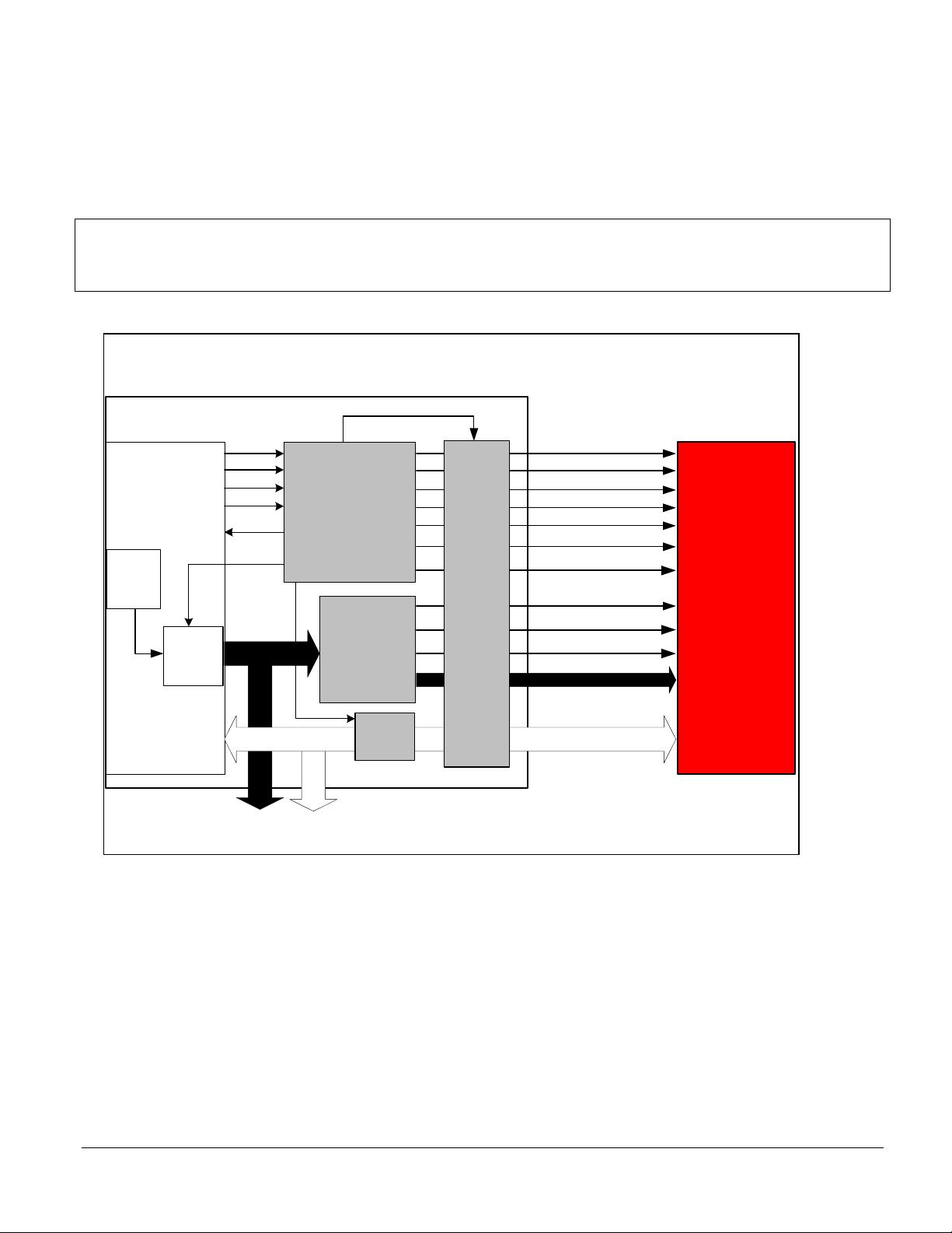
Figure 1 illustrates the signal chain between the ADSP-21161N, the controller and the SDRAM itself. The
3 parts for the signal flow to be considered:
• ADSP-21161N (core, DMA, address buffer)
• SDRAM Controller (command logic, address multiplexer, data buffer and clock divider)
• SDRAMemory
Figure 1: Signal chain: A DSP- 21 161 N t o S DRAM
ADSP-21161N
Core
DMA
CCLK
int. RD
int. WR
int. Reset
int. ACK
Address
buffer
busy
SDEMx
A27:0
A23:0
(non SDRAM)
m
o
C
A
SDBUF
D47:16
m
a
o
L
d
d
M
d
n
c
i
g
s
s
e
r
p
i
t
l
u
SDCKR
CCLK
SDCKE
~RAS
~CAS
~SDWE
DQM
SDA10
~MSx
A14
r
e
x
A13
e
l
A9:0,
A12:11
Data
buffer
Divider
Unit
CCLk
or
CCLK/2
max. 100 MHz
CLK
CKE
~RAS
~CAS
~WE
DQM
A10
SDRAM
~CS
BA0
BA1
A9:0,
A12:11
DQ31:0
2 – On-Chip Controller Architecture
The synchronous interface between the ADSP-21161N and the on-chip controller can be described in 3
basic parts:
2.1 – Command Logic
Because of the 2 different timing protocols, the internal SHARC commands are converted to comply with
the JEDEC standard for SDRAMs. The SDCLK clock, maximum 100 MHz, is used for synchronous
operation. The SHARC’s internal request lines or strobes are used to access the SDRAM with pulsed
The ADSP-21161 SHARC® On-chip SDRAM Controller (EE-163) Page 4 of 50
a
commands. The controller’s internal acknowledge signal inserts variable wait states to the DSP during
overhead cycles, caused by DRAM technology.
2.2 – SHARC Address Buffer
The SHARC’s address buffer enables the controller activation depending on bank assignment and external
address. The SHARC’s address pipeline depth is 1; therefore address pipelining is not supported.
2.3 – Address Multiplexer
Every first read or write action is issued in multiplexed mode. A maximum of 8192 Rows (13 addresses)
within 2048 columns (11 addresses) can be addressed. Furthermore, A[14:13] lines are used to select the
current SDRAM bank.
2.4 – Data Buffer
If systems incorporate a heavy busload, additional data buffers are used to decouple the input from the
capacitive load. The internal data buffer in conjunction with an external buffer reduce additional logic to a
minimum.
2.5 – Clock Divider
The clock divider unit controls the SDRAM with core or core half speed.
2.6 – I/O Capability
The system is designed to support up to 32-bit I/O over the external port. For code execution, the shared
linkports (I/O 16-bits) can be used to get a maximum I/O of 48-bit. The controller doesn’t know about the
connected I/O size.
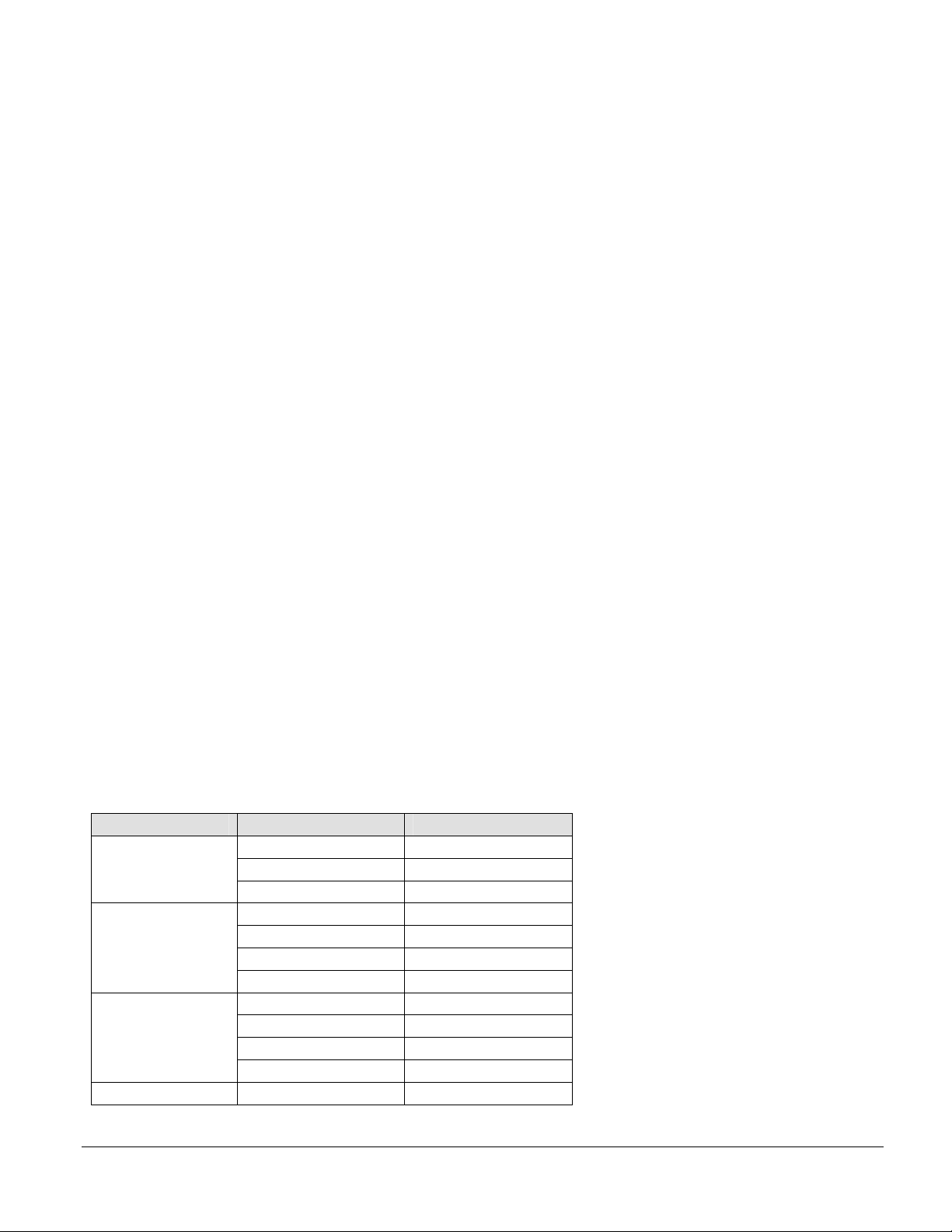
2.7 – SDRAM Types
The interface supports various LVTTL SDRAMs depending on size and organization (I/O capability and
pages size).
Size I/O capability Page size
1M x 16 256
16-Mbits
2M x 8 512
4M x 4 1024
2M x 32 256
64-Mbits
4M x 16 256
8M x 8 512
16M x 4 1024
4M x 32 256
128-Mbits
8M x 16 512
16M x 8 1024
32M x 4 2048
256-Mbits 8M x 32 256
The ADSP-21161 SHARC® On-chip SDRAM Controller (EE-163) Page 5 of 50
a
d
d
d
d
d
d
16M x 16 512
32M x 8 1024
64M x 4 2048
2.8 – Control Registers
3 memory mapped register control the whole interface:
• Wait Register (access mode)
• SDRDIV Register (refresh counter)
• SDCTL Register (control of SDRAM controller and SDRAM)
3 – Command Coding
This chapter covers all kind of information related to control the SDRAM.
Note: All SDRAM commands are fully transparent to the user.
3.1 - Pin Description of Controller
For pin description of the interface ([1], pg.8-7)
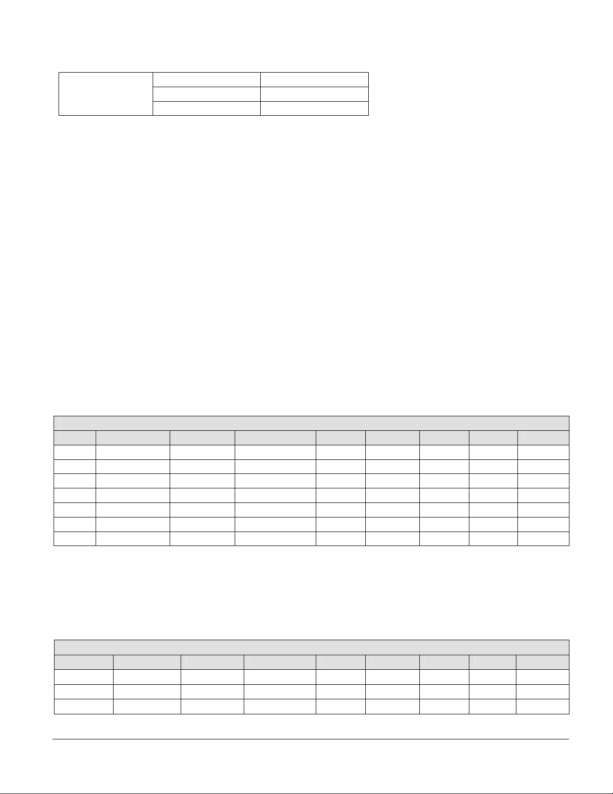
3.2 - Controller Command Truth Table
This section provides a table to get an overview of all commands provided by the SDRAM controller.
Commands SDCKE sampled high
SDCKE(n-1) SDCKE(n) A[0-9,11-14] SDA10 ~MS[0-3] ~RAS ~CAS ~SDWE
MRS 1 1 Vali
ACT 1 1 Vali
RD 1 1 Vali
WR 1 1 Vali
Vali
Vali
0 0 0 0
0 0 1 1
0 0 1 0 1
0 0 1 0 0
DESL 1 1 X X 1 X X X
PREA 1 1 X 1 0 0 1 0
REF 1 1 X X 0 0 0 1
X=don’t care, 0=logic 0, 1=logic 1
These commands are handled automatically by the interface.
While the SDCKE line toggles in asynchronous manner, the commands are sampled synchronous to the
CLK signal.
Commands with Transition of SDCKE
SDCKE(n-1) SDCKE(n) A[0-9,11-14] SDA10 ~MS[0-3] ~RAS ~CAS ~SDWE
SREF En 1 0 X X 0 0 0 1
SREF Ma 0 0 X X X X X X
SREF Ex 0 1 X X 1 X X X
The ADSP-21161 SHARC® On-chip SDRAM Controller (EE-163) Page 6 of 50
a
r
d
X=don’t care, 0=logic 0, 1=logic 1, En=entry, Ma=maintain, Ex=exit
Note: Power-down, Suspend mode and auto precharge are not supported.
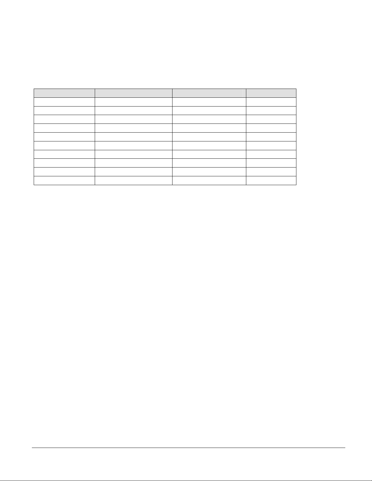
3.3 – Relevant Specs
Timing Spec Description Configuration Register
CCLK core clock 20-100 MHz peripheral
TREF row
TRAS active to precharge 1-15 cycles SDCTL
TRCD RAS to CAS delay 1-7 cycles SDCTL
TRP precharge to active 1-7 cycles SDCTL
TDRD dummy reads 2 + CL cycles Fixed
TRC(TRFC) row refresh cycle TRC=TRAS+TRP SDCTL
TMRD(TRSC) MRS to active 2 cycles Fixed
TXSR self- to auto refresh 2 + TRC cycles Fixed
CL read (CAS) latency 1-3 cycles SDCTL
3.4 - Simplified State Diagram
The state diagram is useful to analyze all deterministic sequences. Figure 4 shows all possible states:
efresh perio
0-0xFFFF SDRDIV
3.5 – Setup and Hold Times
The synchronous operation uses the SDCLK as reference. Commands, addresses and data are latched at
the rising edge of SDCLK. The valid time margin around the rising edge is defined as setup time (time
before rising edge) and hold time (time after rising edge) to guarantee that both the controller and the
SDRAM are working reliably together. Signal’s- slew rates, propagation delays (PCB) and capacitive
loads (devices) influence these parameters and should be taken into consideration [2].
The ADSP-21161 SHARC® On-chip SDRAM Controller (EE-163) Page 7 of 50
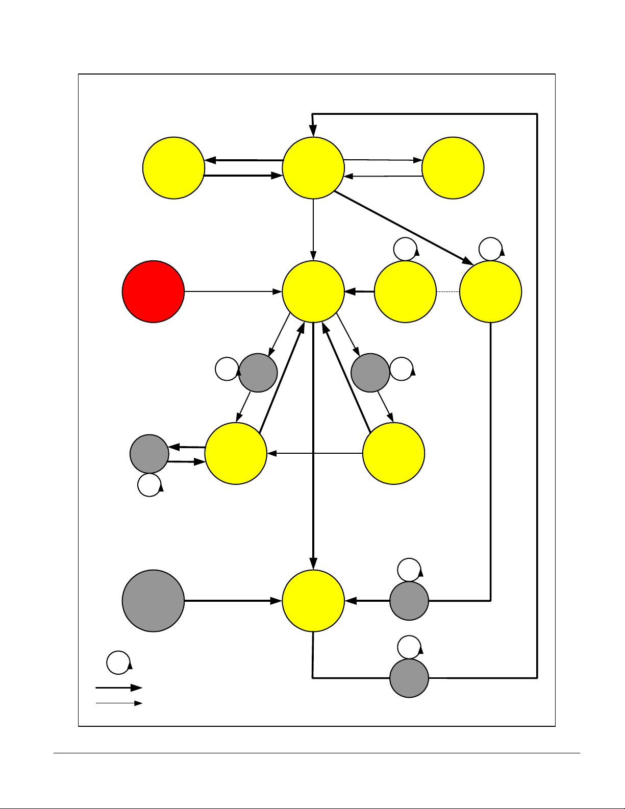
Figure 4: Simplified State Diagram: ADSP-21161N SDRAM Controller
a
Mode
Register
Core
IOP
MMS
Host
CL
1-3
MRS SREF
tMRD=2 tXSR=2+tRC
DESL
RD
tRCD
1-7
Single
Read
L
S
E
D
Idle
State
ACT
Row
activate
RD
DESL
WR
D
E
S
L
Exit
tRCD
1-7
Single
Write
REF
SDRDIV
Counter
expired
Self
Refresh
Auto
Refresh
PREA
Controller works in burst length 1
only one bank at the time
can be active
set bit
SDPSS in
IOCTL
Core Cycles, CL in SDCLK
Automatic sequence
User sequence
PREA
Pre-
charge
all
tRAS
1-15
tRP
1-7
The ADSP-21161 SHARC® On-chip SDRAM Controller (EE-163) Page 8 of 50
a
4 – Hardware Properties
The next properties apply for the ADSP-21161N:
4.1 – SDRAM Interface Speed Control
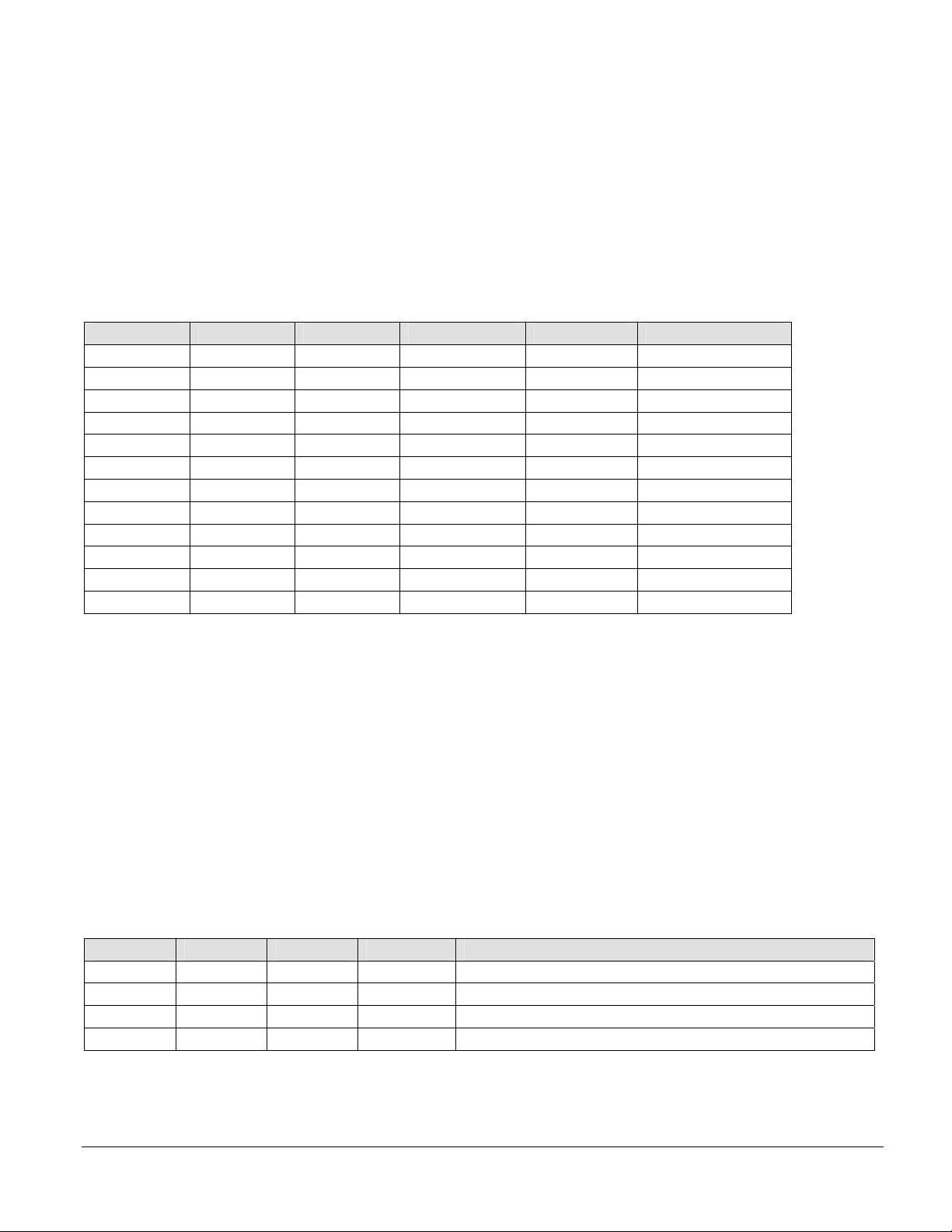
The pins CLKIN/XTAL, CLK_CFG[1:0] and ~CLKDBL affect the speed of SDRAM interface.
Additional, the SDCKR-bit influences the speed as well. The ID number must be 0 or 1 for an uniprocessor system, otherwise the SDCLK[0:1] are not driven (BSYN-bit / SYSTAT must be set). Next
table shows 12 different possibilities for speed configuration:
CLK_CFG1 CLK_CFG0 ~CLKDBL CLKIN:CCLK SDCKR-bit CLKIN:SDCLK
0 0 1 1:2
0 1 1 1:3
1 0 1 1:4
0 0 1 1:2
0 1 1 1:3
1 0 1 1:4
0 0 0 1:4
0 1 0 1:6
1 0 0 1:8
0 0 0 1:4
0 1 0 1:6
1 0 0 1:8
1 1:2
1 1:3
1 1:4
0 1:1
0 1:3/2
0 1:2
1 1:4
1 1:6
1 1:8
0 1:2
0 1:3
0 1:4
Different settings can result in the same speed for the SDRAM interface. Which settings are useful
depends on the used peripherals. The CLKOUT clock samples internal the SRAM, host, IRQs and IOFlags interfaces and are affected by the CLKIN input and ~CLKDBL pin, not the CLK_CFGx pins. ([2],
pg.20). This will help to balance the system and to find the best ratio between CLKOUT, Core clock and
SDRAM clock.
Note: The SDRAM interface is internally sampled with core cycles.
4.2 – SDRAM Clock Control
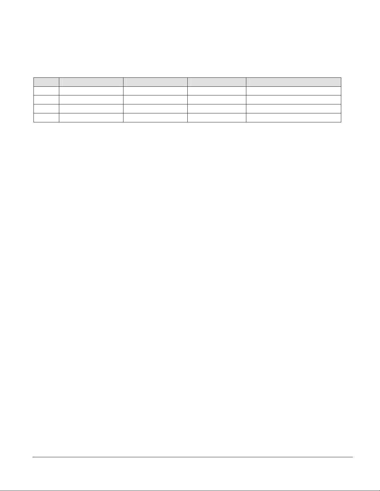
The SDRAM clock is provided by the DSP, not by an external clock oscillator. Even if the SDRAM
interface is disabled, the SDCLK0 and SDCLK1 are driven out of reset. You can vary the clock between
CCLK/2 or CCLK (SDCKR bit in SDCTL). The DSDCTL and DSDCK1 SDCTL control the SDRAM
clock pins.
DSDCK1 DSDCTL SDCLK0 SDCLK1 Comment
0 0 CCLK/2 CCLK/2 Both clocks active (reset value)
0 1 Hi-Z CCLK/2 SDCLK0 and control disabled, SDCLK1 enabled
1 0 CCLK/2 Hi-Z SDCLK0 and control enabled, SDCLK1 disabled
1 1 Hi-Z Hi-Z SDRAM Interface disabled
If SDRAM interface is not used, set both bits DSDCTL and DSDCK1 to 1, the bits SDEMx=000. This
allows the ~MSx banks to be used for other memory types.
The ADSP-21161 SHARC® On-chip SDRAM Controller (EE-163) Page 9 of 50
a
4.3 – SDRAM Address Space
All 4 ~MS[3-0] banks support SDRAM. As the external port supports 24 address bits, some restrictions
apply.
Bank V-Field A[26-27] E-Field A[21-23] Size Comment
0 00 111 62.68 Mwords Part of internal memory
1 10 000 64 Mwords
2 01 000 64 Mwords
3 11 000 64 Mwords
For bank 0, the controller issues external address starting at 0x200000, A[21]=1 to the SDRAM, but the
virtual addresses A[26:27] are still zeros. Addresses smaller 0x200000 are not accessible in bank 0 and
represent MMS and internal memory.
4.4 – Address Mapping Scheme
Basically, there are various possibilities accessing the SDRAM, for instance you access all rows in a bank
sequentially or you access all banks in a row sequentially. PC DIMM modules are accessed different by
its controller compared to a typical DSP application. The ADSP-21161 controller uses a hardware map
scheme optimized for digital signal processing ([1], pg.8-26).
Note: The address map scheme allows you to understand the system’s performance.
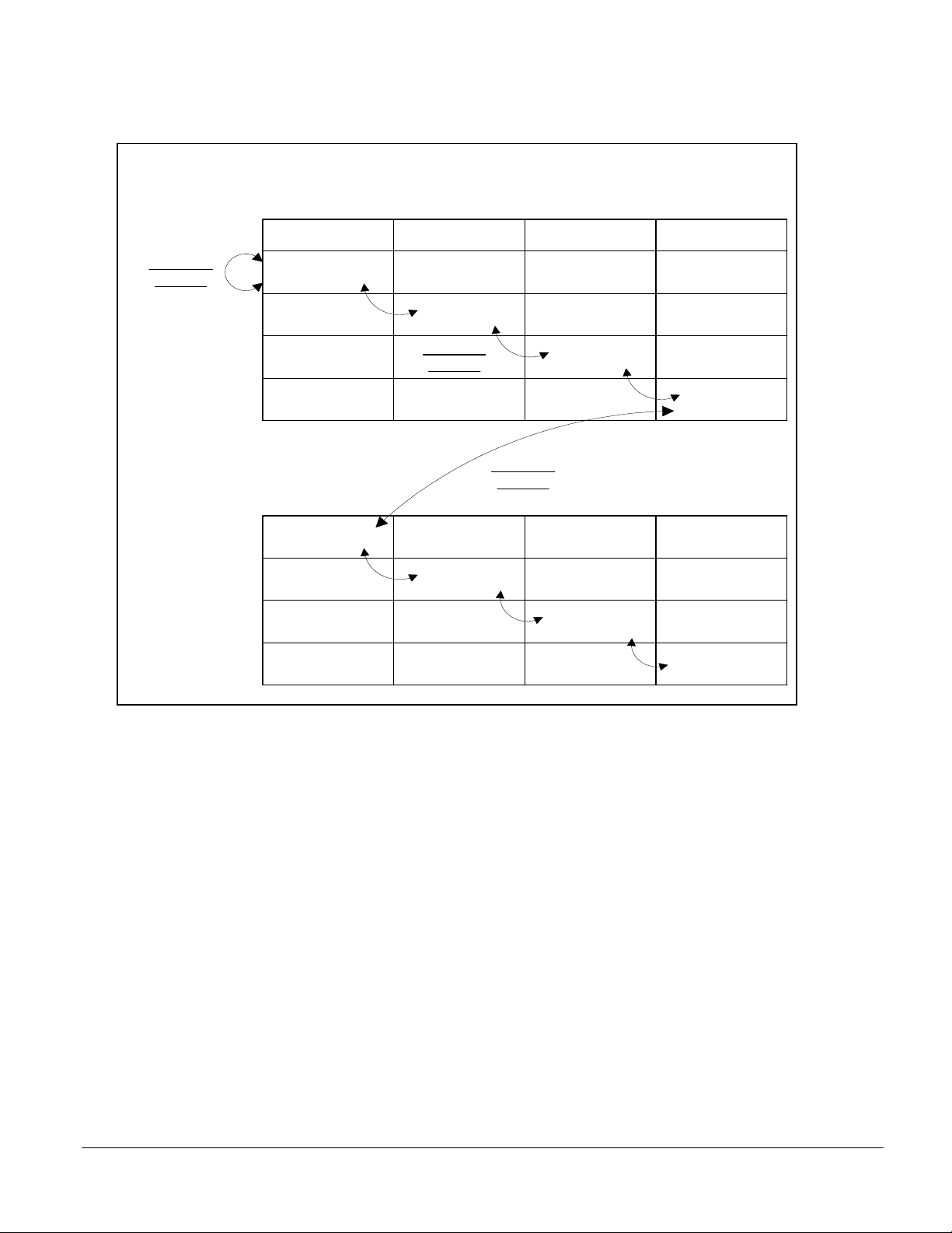
Two control bits (SDBN- and SDPGS-bits / SDCTL) are used to program the address map scheme for
different memory organizations. Figure 2 reproduces an example of the controller’s address mapping. In
page 0, the SDRAM’s banks A to D are sequentially selected. As bank interleaving is not supported, every
bank access in the same page has the overhead as an access between 2 pages. The address region of a full
page for instance 0x200000 to 0x2003FF (1024 words) can be accessed with 1 cycle/word.
The ADSP-21161 SHARC® On-chip SDRAM Controller (EE-163) Page 10 of 50
a
Figure 2: Controller Address Mapping to bank 0 of ADSP-21161N
4M x 4bit x 4, Page size 1024 words
Bank_A Bank_B Bank_C Bank_D
On Page
Access
g
a
P
e
g
a
P
0x200000
0x2003FF
0x200400
0
e
0x2FFF000
0x2FFF3FF
5
9
0
4
0x2007FF
Off Bank
Access
0x2FFF400
0x2FFF7FF
0x200800
0x200BFF
0x200C00
0x200FFF
Off Page
Access
0x2FFF800
0x2FFFBFF
0x2FFFC00
0x2FFFFFF
Note: Only one bank at a time can be active. Off-bank and off-page access have the same overhead.
4.5 – SDRAM Transfer Interruption
The pins CLK_CFG[1:0], ~CLKDBL and SDCKR-bit influence the SDRAM transfer interruptions. If
SDRAM accesses (reads or writes) are interrupted, the controller inserts stall cycles (DESL) to match with
the internal timing boundary based on CLKIN cycles ([1], pg.8-25).
4.6 – Interface during Reset
SDRAM interface status ([1], pg.13-20).
4.7 – Extended Precision
The PX-register allows core transfers of 40/48-bit to internal and external memory. This requires the
setting of IPACK-bit zero in SYSCON to enable 3 column accesses to SDRAM/SBSRAM or SRAM ([1],
pg.5-13).
The ADSP-21161 SHARC® On-chip SDRAM Controller (EE-163) Page 11 of 50

a
4.8 – Circular Access
The controller supports the circular buffer during core access for sequential read or writes in the whole
page, performing a throughput of 1 cycle/word in the boundary.
Note: This functionality is similar to the DAG’s circular buffering mode.
5 – Command Properties
5.1 – Mode Register Set (MRS)
The controller fixes following spec of SDRAM:
Burst length: one
Burst type: sequential
The controller uses no burst mode (burst length one) only. Every read or write command is accompanied
with an external address by the controller.
Note: every SDRAM vendor supports Burst length 1.
5.2 – Deselect (DESL)
Each SHARC bank ~MS[0-3] can be mapped in the memory region of the SDRAM. All 4 SHARC banks
can be connected (bit SDEMx / SDCTL) to the interface. The DESL command has the same functionality
as the NOPs; furthermore, next table lists the different situations in which the DESL occurs:
DESL truth table
• Non-external SDRAM access (access to another SHARC bank)
• Core access (e.g. computation unit, interrupt, cache, DAG)
• DMA operation (higher priority request of IOP)
• SDRDIV counter expired (refresh period counter)
• SDRAM read to write transition
• SDRAM off page and off bank access
• ~HBR asserted (host interface)
• ~BRx asserted (multiprocessing)
5.3 – I/O Mask Function (DQM)
It’s used to disconnect the SDRAM’s I/0 buffer to avoid data contention. The affect latency is zero cycles.
The truth table for DQM:
The ADSP-21161 SHARC® On-chip SDRAM Controller (EE-163) Page 12 of 50
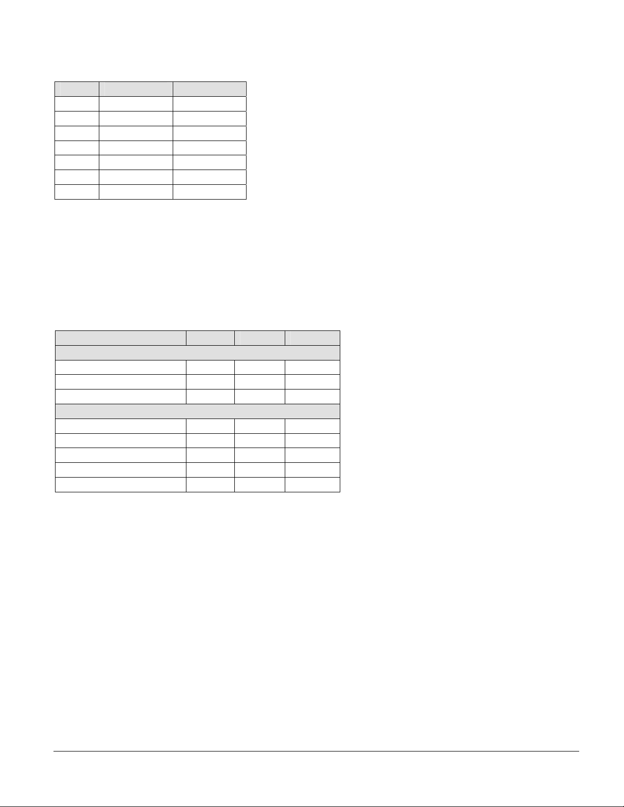
a
SDCKE(n) DQM
MRS 1 1
ACT 1 0
RD 1 0
WR 1 0
DESL 1 0
PREA 1 1
REF 1 0
The controller simply disables the I/O buffer during MRS and PREA command.
Note: The controller does not support partial writes. Therefore, all DQM lines (e.g. DQMH and DQML)
should simply be tied together.
5.4 – SDRAM Bank Select
The controller uses the addresses 13 and 14 for the SDRAM bank selection. The next tables show the truth
table with SDA10, A14 and A13:
Banks A[13] A[14] SDA10
SDRAM with 2 banks
Bank_A - 0 0
Bank_B - 1 0
Both Banks - x 1
SDRAM with 4 banks
Bank_A 0 0 0
Bank_B 0 1 0
Bank_C 1 0 0
Bank_D 1 1 0
All Banks x x 1
x=don’t care, 0=logic 0, 1=logic 1
Note: A14 must be used for 2-banked memories.
Note: It doesn’t matter if you connect A[14:13] to BA[1:0] or A[14:13] to BA[0:1].
5.5 – SDRAM Address 10 (SDA 10)
It provides a special solution to gain refresh control about the SDRAM (without control of address bus) in
host mode. It must be connected with the SDRAM’s A10 pin. This pin has multifunctional character:
depending on the command, it acts as an address (MRS and ACT) or as a command (RD, WR and PREA).
Note: This pin replaces the DSP’s A10 pin during SDRAM accesses only.
5.6 – Write (WR)
Write operations do not use address pipelining. No stall cycles will be inserted.
The ADSP-21161 SHARC® On-chip SDRAM Controller (EE-163) Page 13 of 50

a
5.7 – Read (RD)
The SHARC architecture doesn’t support address pipelining. The next address will only be latched when
the previous data are driven off-chip. For sequential reads, the controller simply applies the command and
address assuming that it will be sequential. For non-sequential reads, it inserts additional dummy reads in
order to reject the data given out by SDRAM, if the next address from the core is non-sequential. It
applies to:
• Non sequential reads
• Sequential reads interruption
• Read to write transition
5.8 – Precharge All (PREA)
This command precharges all banks of the SDRAM simultaneously (SDA 10 high to select all banks),
which returns the banks in idle state.
Note: The controller doesn’t support precharge of single bank while only one bank at the time is active.
5.9 – Auto Refresh (REF)
The auto- or CAS before RAS- refresh requires only a command, no addresses. After the SDRAM
registers the command, it asserts internally CAS and delays RAS to execute a single row refresh. Up to 4
SHARC banks are simultaneously refreshed with ~MS[3:0].
Note: The controller doesn’t support burst refresh.
5.10 – Self Refresh (SREF)
The self-refresh is a very effective way to reduce the application’s power consumption to a minimum. The
device can run in this mode during long non-SDRAM operations. This mode is used to set the SDRAM
and SDRAM-controller in “stand-by”. The device starts refreshing itself triggered by an internal timer.
Additional, only this command allows the transition to another SDRAM controller during run-time.
6 – Shared Memory
This section covers the arbitration logic used to guarantee multiprocessing systems including SDRAM as
shared memory. The ADSP-21161N can be connected to a multi-processor cluster of six. Only one
SHARC can drive the bus at the time to the SDRAM. The interface works bi-directional (BSYN-bit /
SYSTAT set for ID=1-6) in order to detect commands MRS, REF and SREF and PREA. For systems with
heavy busload, you can use both clock outputs (e.g. SDCLK0 for LSB data and SDCLK1 for MSB data).
It is not allowed to use only SDCLK1 in a cluster system, because SDCLK1 is limited to an output
(unidirectional).
6.1 – MRS
Power up sequence can be done by any of six DSPs. Since broadcast write is not supported on ADSP21161N, all six DSPs must set the bit SDPSS/ SDCTL, the one which has the bus mastership, will do
power-up. The slaves recognize power-up with the MRS and clear its read-only SDPSS bit.
Note: For multiprocessing, the MRS is issued once.
The ADSP-21161 SHARC® On-chip SDRAM Controller (EE-163) Page 14 of 50

a
6.2 – REF
This detection helps to synchronize all six refresh counters. The slave’s SDRDIV counter will be
decremented each time the interface detects a refresh. This feature guarantees a periodic refresh and
requires the exact same settings of SDRDIV and SDCTL registers.
Note: For multiprocessing, the control settings must be identical for each DSP.
6.3 – SREF
This detection helps to synchronize the self-refresh base. The master’s bit SDSRF brings the whole
system in self-refresh mode. The slave recognizes the SREF and set therefore its bit SDSRF. The current
SDRDIV counters will be frozen until the self-refresh is exited.
6.4 – PREA
The BTC is used to arbitrate between the maximum of six controllers. Because the new SDRAM
controller doesn’t know which row in the SDRAM was accessed before busmastership, it only executes a
PREA if the previous had accessed SDRAM.
7 – Programming the SDRAM Interface
7.1 – Guideline
When programming the interface depends on the application: If you need it for storage of boot memory,
the initialization must be placed in the dedicated loader files to ensure proper booting. If you use memory
dynamically in your system for data storage, the init sequence can be placed in the user code.
The Interface is programmed in following order:
1. WAIT Register (wait states count)
2. SDRDIV Register (setting the row refresh period value)
3. SDCTL Register (contains programmable SDRAM control bits)
7.2 – Wait Register (Wait States)
For proper internal handshake between core/DMA and controller, make sure that the wait state count
EBxWS (WAIT register) is set to zero ([1], pg.A-77).
The memory access mode EBxAM (WAIT register) becomes regardless for SDRAM as it is defined with
the SDEMx-bit / SDCTL. The ACK signal should not be de-asserted during SDRAM and SBSRAM
accesses. ACK should only be de-asserted during SRAM accesses ([1], pg.7-41).
7.3 – Refresh Counter (SDRDIV)
This counter enables applications to coordinate the clock rate with the SDRAM’s required refresh rate.
The SDRDIV register is used to enter the row refresh period in number of core cycles calculated in the
equation.
Following specs are related to the vendor’s datasheet:
The ADSP-21161 SHARC® On-chip SDRAM Controller (EE-163) Page 15 of 50
 Loading...