


Hardware Rev. 2.2
ADSP-21160 EZ-KIT Lite™
User Guide
Part Number 500-00546
© 2000 Analog Devices, Inc.
ALL RIGHTS RESERVED
Analog Devices, Inc.
Digital Signal Processing Division
One Technology Way
P.O. Box 9106
Norwood, MA 02062-9106
(617) 329-4700

Copyright Information
© 1996-2000 Analog Devices, Inc., ALL RIGHTS RESERVED. This document may not
be reproduced in any form without prior, express written consent from Analog Devices,
Inc.
Disclaimer
Analog Devices, Inc. reserves the right to change this product without prior notice.
Analog Devices believes all information furnished to be accurate and reliable. However,
Analog Devices assumes no responsibility for its use; nor for any infringement of patents
or other rights of third parties, which may result from its use. No license is granted by
implication or otherwise under the patent rights of Analog Devices.
Trademark and Service Mark Notice
The Analog Devices logo, SHARC, the SHARC logo, TigerSHARC, the TigerSHARC
logo, and EZ-LAB are registered trademarks; and VisualDSP++, theVisualDSP++ logo,
EZ-KIT Lite, Apex-ICE, Mountain-ICE, Summit-ICE, and Trek-ICE are trademarks of
Analog Devices, Inc.
Microsoft and Windows are registered trademarks and Windows NT is a trademark of
Microsoft Corporation. Pentium is a trademark of Intel Corporation.
Adobe and Acrobat are registered trademarks of Adobe Corporation.
All other brand and product names are trademarks or service marks of their respective
owners
The ADSP-21160 EZ-KIT Lite evaluation board contains ESD
(electrostatic discharge) sensitive devices. Electrostatic charges
readily accumulate on the hu man body and equipment and can
discharge without detection. Permanent damage may occur to devices
subjected to high energy discharges. Proper E SD precautions are
recommended to avoid performance degradation or loss of
functionality. Unused boards should be stored in the protective
shipping package.
Board products with the CE marking – shown on the right – comply
with the EMC Directive (89/336/EEC). Compliance with this
directive implies conformity to the following European Norms:
• EN55022 (CISPR 22) Radio Frequency Interference, Class A
• EN50082-1 Electromagnetic Immunity
The product also fulfills EN60950 (product safety) which is
essentially the requirement for the Low Voltage Directive
(73/23/EEC).
WARNING!
ESD SENSITIVE DEVICE
ADSP-21160 EZ-KIT Lite

Table of Contents
Table of Contents
1 Introduction ...........................................................................................1
1.1. Overview .............................................................................................................1
1.2. System Architecture ............................................................................................ 3
1.3. What the kit contains........................................................................................... 4
1.4. The ADSP-21160 ADSP-21160 EZ-KIT Lite Board ............................................5
1.5. Reference Material .............................................................................................. 6
2 Getting Started ......................................................................................7
2.1. Installation Overview ........................................................................................... 7
2.2. Requirements ...................................................................................................... 8
2.3. Hardware Installation...........................................................................................9
2.4. Software Installation .......................................................................................... 11
2.5. Verifying the installation.....................................................................................11
2.5.1. Power-on Self Test (POST) .............................................................. 12
2.5.2. Parallel Port Setup ............................................................................13
3 Demonstration Programs...................................................................17
3.1. Overview ...........................................................................................................17
3.2. Starting the VisualDSP++ Debugger.................................................................17
3.3. Debugger Operation with the ADSP-21160 EZ-KIT Lite ................................... 17
3.3.1. Loading and Running Programs .......................................................18
3.3.2. Registers and Memory......................................................................20
3.3.3. Resetting the Board .......................................................................... 21
3.4. Demonstration Programs ..................................................................................21
3.4.1. Fft.dxe ...............................................................................................22
3.4.2. BP.dxe ..............................................................................................27
3.4.3. Pluck.dxe ..........................................................................................29
3.4.4. Primes.dxe ........................................................................................30
3.4.5. Tt.dxe ................................................................................................31
4 Hardware Description.........................................................................33
4.1. Processor and Core Components ..................................................................... 34
4.1.1. Oscillators .........................................................................................34
4.1.2. CODEC .............................................................................................35
4.1.3. Power Supply.................................................................................... 35
4.1.4. PLD ...................................................................................................37
4.1.5. Flash Memory ................................................................................... 37
ADSP-21160 EZ-KIT Lite
i

Table of Contents
4.1.6. SBSRAM ........................................................................................... 37
4.1.7. Processor..........................................................................................37
4.2. Connectors ........................................................................................................ 38
4.2.1. Serial Ports........................................................................................39
4.2.2. Link Ports ..........................................................................................40
4.2.3. Power Supply Connector ..................................................................40
4.2.4. Audio Connectors .............................................................................40
4.2.5. JTAG Connector ...............................................................................41
4.2.6. Cluster Connectors ...........................................................................41
4.2.7. Parallel Port.......................................................................................41
4.3. Push Buttons / LEDs ......................................................................................... 42
4.3.1. Master Reset Push Button (RESET PB) ........................................... 43
4.3.2. User Push Buttons (PB0, PB1, PB2, PB3) .......................................43
4.3.3. User LEDs (D1, D2, D3) ...................................................................43
4.3.4. Power LEDs (D4, D5, D6).................................................................44
4.4. Configuration Switches......................................................................................44
4.4.1. Clock Routing Switch (SW1)............................................................. 47
4.4.2. SBSRAM Configuration Switch (SW2)..............................................47
4.4.3. Parallel Port Configuration Switch (SW7) .........................................47
4.4.4. Clock Configuration Switch (SW9).................................................... 48
4.4.5. Board ID Switch (SW10) ...................................................................49
4.4.6. Boot Mode Switch (SW11) ................................................................ 50
4.4.7. IRQ Routing Switch (SW12) .............................................................50
4.4.8. FLAG Routing Switch (SW13) ..........................................................50
4.5. Test Points ........................................................................................................51
5 Operation............................................................................................. 53
5.1. Overview ...........................................................................................................53
5.2. Power-on Self Test (POST) ..............................................................................53
5.2.1. Flash EPROM ...................................................................................54
5.2.2. External SBSRAM and Internal SRAM .............................................54
5.2.3. CODEC .............................................................................................54
5.3. Monitor Program Operation...............................................................................54
5.4. Interrupts ...........................................................................................................55
5.5. Breakpoints and Stepping .................................................................................56
5.6. Hardware Stacks ............................................................................................... 56
5.7. Benchmarking Utilities.......................................................................................57
6 Programming Reference ....................................................................59
6.1. Memory Map .....................................................................................................59
6.2. Support Library..................................................................................................62
SHARC_OpenSerPort1() ..................................................................................63
SHARC_CloseSerPort1() .................................................................................. 64
HHEZL_SetupCodec() ......................................................................................65
ii ADSP-21160 EZ-KIT Lite

Table of Contents
HHEZL_TransmitToCodec() .............................................................................66
HHEZL_TransmitReadToCodec()..................................................................... 67
HHEZL_ReadFromCodec()............................................................................... 68
HHEZL_WriteCodecReg() ................................................................................69
SHARC_SetLed() .............................................................................................. 70
6.3. Creating and Running Your Own Programs with VisualDSP++ ........................71
6.3.1. Create a New Project File .................................................................72
6.3.2. Set Target Processor Project Options ..............................................72
6.3.3. Edit and Add Project Source Files ....................................................73
6.3.4. Customize Project Build Options ......................................................76
6.3.5. Build a Debug Version of the Project ................................................ 76
6.3.6. Execute and Debug the Project ........................................................76
6.4. EZFlash programmer ........................................................................................77
6.5. Creating Assembly Language Program ............................................................77
6.6. Restrictions on Using the Monitor Executive.....................................................81
7 Forming a Cluster................................................................................83
7.1. Signal Routing in a Cluster................................................................................83
7.2. Example Cluster Configuration .........................................................................84
7.2.1. Identify the Boards and their JTAG positions....................................84
7.2.2. Configure SBSRAM allocation .......................................................... 84
7.2.3. Select the clock sources and multipliers........................................... 85
7.2.4. Assign responsibility for handling the parallel port ............................86
7.2.5. Designate Distribution of IRQs and Flags.........................................86
7.2.6. Set the Boot Source..........................................................................87
8 Connector Pinouts..............................................................................89
8.1. Parallel Port Connector ..................................................................................... 89
8.2. Parallel Port Cable ............................................................................................90
8.3. Link Port Connectors.........................................................................................91
8.4. Link Port Cable..................................................................................................92
8.5. Serial Port Connector ........................................................................................ 93
8.6. Serial Port Cable ............................................................................................... 93
8.7. JTAG Header ....................................................................................................94
8.8. Cluster Connectors ...........................................................................................95
8.9. Desktop Power Connector ................................................................................99
8.10. Line In Connector .............................................................................................. 99
8.11. Line Out Connector ........................................................................................... 99
8.12. Mic In Connector ............................................................................................... 99
8.13. Power Supply Module........................................................................................99
8.14. PLD Footprint .................................................................................................. 100
ADSP-21160 EZ-KIT Lite
iii

Table of Contents
9 Specifications.................................................................................... 101
9.1. Electrical Specifications................................................................................... 101
9.2. Mechanical Specifications ...............................................................................101
9.3. Environmental Specifications ..........................................................................101
9.4. CE Compliance ...............................................................................................101
10 Bill of Materials ................................................................................. 103
11 Schematics........................................................................................ 105
12 Index ................................................................................................. 117
iv ADSP-21160 EZ-KIT Lite

List of Tables
List of Tables
Table 1 Factory Settings - Configuration Switches.............................................. 46
Table 2 Interrupt Vector Assignment ...................................................................56
Table 3 Known Restrictions with the Monitor Program........................................ 81
List of Figures
Figure 1 ADSP-21160 EZ-KIT Lite Board Architecture .........................................3
Figure 2 ADSP-21160 EZ-KIT Lite Board Solder Side ..........................................5
Figure 3 ADSP-21160 EZ-KIT Lite Board Component Side .................................. 5
Figure 4 Hardware Installation...............................................................................9
Figure 5 Master Reset Pushbutton......................................................................21
Figure 6 FFT Example Board Setup....................................................................22
Figure 7 Band Pass (BP) Example Board Setup................................................. 27
Figure 8 Pluck Example Board Setup.................................................................. 29
Figure 9 Talk Thru Example Setup......................................................................31
Figure 10 Core Component Locations................................................................. 34
Figure 11 Connector Locations ...........................................................................38
Figure 12 Serial Port Routing ..............................................................................39
Figure 13 Link Port Routing.................................................................................40
Figure 14 Push Button and LED Locations .........................................................42
Figure 15 Configuration Switches........................................................................ 44
Figure 16 Test Points ..........................................................................................51
Figure 17 CODEC Signal Pin Assignments......................................................... 52
Figure 18 ADSP-21160 Memory Addressing ......................................................59
Figure 19 ADSP-21160 Internal Memory Space .................................................60
Figure 20 ADSP-21160 Memory Space Allocation..............................................61
ADSP-21160 EZ-KIT Lite
v

List of Figures
vi ADSP-21160 EZ-KIT Lite

Introduction
1 Introduction
1.1. Overview
The Analog Devices ADSP-21160 processor used in the ADSP-21160 EZ-KIT Lite® has
many features integrated onto a single digital signal processor (DSP) chip. The processor
features include:
• Super Harvard Architecture: four independent internal buses for dual data fetch;
instruction fetch, and non-intrusive, zero-overhead I/O
• Single-Instruction-Multiple-Data (SIMD) computational architecture: two 32-
bit single-precision (or 40-bit extended precision) IEEE floating-point and 32-bit
fixed-point computation units, each with its own ALU, multiplier, shifter and register
file (100-MIPS, with 600 MFLOPS peak, 400 MFLOPS sustained)
• 12.5 ns core instruction rate: single-cycle instruction execution, including SIMD
operations in both computation units
• Dual Data Address Generators (DAGs) with modulo and bit-reverse addressing
• On-chip, configurable memory banks: dual-ported 4-megabit internal SRAM for
fast, independent local memory access for DSP core, DMA controller and I/O
processor
• Two 40 Mbit/s synchronous serial ports
• Sophisticated DMA controller: 6 simultaneous channels with zero impact on
performance of DSP core
The ADSP-21160 EZ-KIT Lite provides an easy way for you to investigate the power of
the SHARC® family of processors and develop your own applications based on these
high-performance DSPs. The ADSP-21160 EZ-KIT Lite is a complete development
system package that is ideal for getting started in DSP. The ADSP-21160 EZ-KIT Lite
was designed to help you:
• Evaluate Analog Devices’ floating-point DSPs
• Learn about DSP applications
• Develop DSP applications
• Simulate and debug your application
• Prototype new applications
ADSP-21160 EZ-KIT Lite 1

Introduction
The ADSP-21160 EZ-KIT Lite is an ADSP-21160 based development and demonstration
board with full 16-bit stereo audio I/O capabilities. The board’s features include:
• Analog Devices ADSP-21160 DSP running at 80 MHz
• Socketed 40 MHz oscillator with jumper selectable clock multiplier
• Analog Devices AD1881 16-bit Stereo AC’97 SoundMAX® CODEC
• Connectors for CODEC Mic-in, Line-in and Line-out
• Programmable/readable EPROM Flash Memory (4 Mbit)
• Expansion memory 2 banks, 64k x 32 each (4 Mbit total)
• Four User pushbuttons
• Master board Reset pushbutton
• Three User programmable LEDs
• Power supply regulation
• Parallel Port interface for debug and control operations
• External connectors for Link Ports 4 and 5
• External connector for Serial Port 0
• JTAG emulator header
• Cluster Expansion Connectors
The board can run standalone or connect to the parallel port of your PC. A monitor
program running on the DSP in conjunction with a host program running on the PC lets
you interactively download programs as well as interrogate the ADSP-21160. The board
comes with a EPROM so that you can run the monitor program and demonstrations
provided.
The ADSP-21160 EZ-KIT Lite also comes with all the software you need to develop
sophisticated, high-performance DSP applications. A C/C++ compiler, assembler,
run-time libraries and librarian, linker, and debugger are all included.
You can also connect an optional JTAG in-circuit emulator to the ADSP-21160 EZ-KIT
Lite. The emulator allows you to load programs, start and stop program execution,
observe and alter registers and memory, and perform other debugging operations. JTAG
emulators are available from Analog Devices.
The ADSP-21160 EZ-KIT Lite was designed and manufactured by Spectrum Signal
Processing, of Burnaby, BC, Canada, to Analog Devices’ specifications.
ADSP-21160 EZ-KIT Lite
2
Introduction
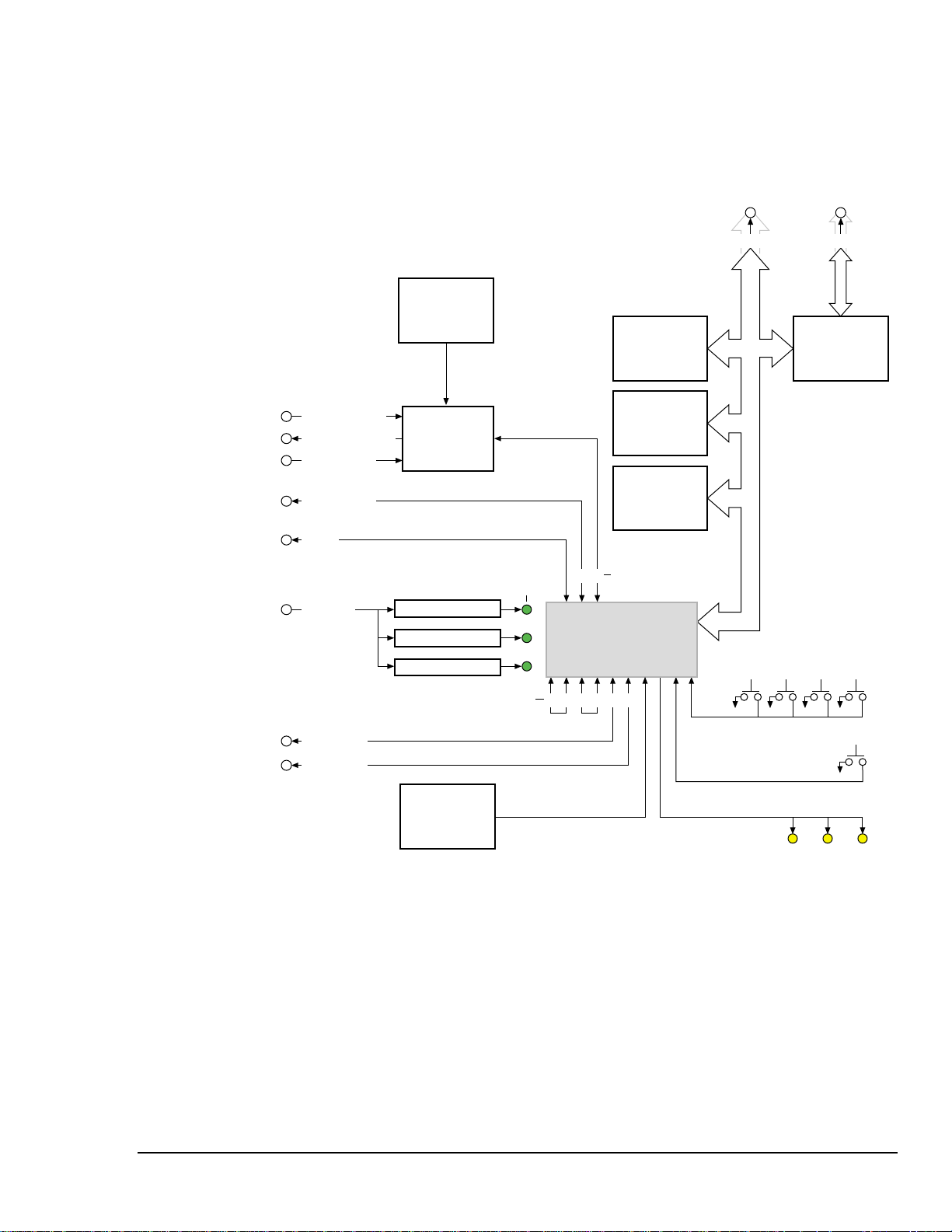
1.2. System Architecture
The block diagram below shows the main features of the ADSP-21160 EZ-KIT Lite
board.
Cluster Connector Parallel Port
Oscillator
24.576 MHz
SBSRAM
64K x 32
Upper Word
PLD
Line In Stereo
Line Out Stereo
Mic In Mono
Serial Port 0
JTAG
POWER
Link Port 4
Link Port 5
CODEC
AD 1881
Regulator 5V
Regulator 3.3V
Regulator 2.5V
Link Ports
Oscillator
40 MHz
Power LEDs
(Green)
ADSP 21160
Processor
0 1 2 3 54
Serial Ports
0 1
S
SBSRAM
64K x 32
Lower Word
Flash
Memory
(4 Mbit)
Cluster Bus
64 Bit
50 Mhz
Interrupt Pushbuttons
Master Reset Pushbutton
User LEDs (Amber)
Figure 1 ADSP-21160 EZ-KIT Lite Board Architecture
The CODEC connects to the processor via serial port 1. Two of the Link Ports are routed
to external connectors. The host port of the processor (64 bit parallel port) connects
directly to the Flash memory and the synchronous burst static RAM (SBSRAM). A
programmable logic device (PLD) interfaces the processor’s external port to the parallel
interface. The push button interrupts are de-bounced and then connected to the dedicated
interrupt pins on the processor. The User LEDs from the processor are driven directly by
the processor Flag pins. The Cluster connectors allow the board to be connected into a
cluster configuration with another ADSP-21160 EZ-KIT Lite board (maximum of 2
boards).
ADSP-21160 EZ-KIT Lite 3

Introduction
1.3. What the kit contains
Your ADSP-21160 EZ-KIT Lite board package contains the following items. If any item
is missing, contact the vendor where you purchased your ADSP-21160 EZ-KIT Lite, or
Analog Devices.
• ADSP-21160 EZ-KIT Lite board
• Power cable with DC power supply
• Parallel port cable
• One CD, containing
− ADSP-21160 EZ-KIT Lite software and examples
− Utilities
− ADSP-21160 EZ-KIT Lite User Guide (this document)
• VisualDSP++® CD
• Registration card - please fill out and return
To fully exercise the board, you may also need one or more of the following accessories:
• Speakers
• Stereo audio source
• Microphone
• Link port cable(s) – Spectrum part number
002-06364, 30cm
If you wish to order a new set of cables for any reason, refer to Analog Devices website
at www.analog.com/industry/dsp/tools/selection.html
.
ADSP-21160 EZ-KIT Lite
4
Introduction
1.4. The ADSP-21160 ADSP-21160 EZ-KIT Lite Board
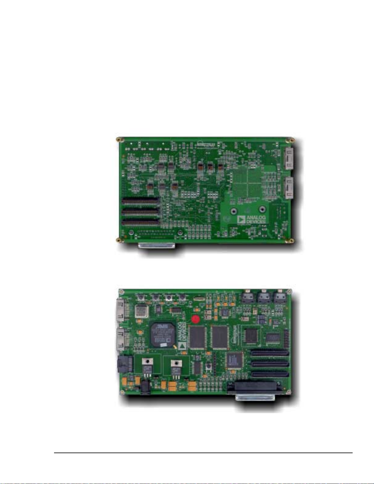
The ADSP-21160 EZ-KIT Lite board measures 4 inches by 6.5 inches (10.16 cm by
16.51 cm), with the active components, LEDs, pushbuttons, signal breakout headers and
connectors on one surface (component side). The reverse side (solder side) contains the
passive components and the configuration switches. The board is designed as a
bench-top evaluation unit, and should be placed on a flat surface, solder side down, to
allow easy access to the pushbuttons and LED’s. Standoff legs on the solder side provide
clearance for the components.
Figure 2 ADSP-21160 EZ-KIT Lite Board Solder Side
Figure 3 ADSP-21160 EZ-KIT Lite Board Component Side
ADSP-21160 EZ-KIT Lite 5

Introduction
The ADSP-21160 EZ-KIT Lite board is pre-configured at the factory, and can be
installed and used directly out of the box.
For a complete description of the components on the board, their locations, and details
see section 4, “Hardware Description”.
If you plan to cluster two boards together, refer to section 7, “Forming a Cluster”, for
requirements and procedures.
1.5. Reference Material
For more information on the ADSP-21160 as well as the components of the ADSP21160 EZ-KIT Lite system, see the following documents:
• ADSP-21160 Hardware Reference Manual
• ADSP-21160 Instruction Set Reference Manual
• ADSP-21160 DSP Microcomputer Data Sheet
• AD1881 Serial Port 16-Bit AC’97 SoundMAX CODEC Data Sheet
The ADSP-21160 processor is supported by a complete set of development tools.
Software tools include a C/C++ compiler, assembler, runtime libraries and librarian,
linker, and debugger. For more information on these tools, see the following documents:
• ADSP-21000 Family Hardware and Software Development Tools Data Sheet
• VisualDSP++ User’s Guide & Reference
• C/C++ Compiler Guide & Reference for the ADSP-2106x Family DSPs
If you plan to use the ADSP-21160 EZ-KIT Lite in conjunction with a JTAG emulator,
refer to the documentation that accompanies that product.
ADSP-21160 EZ-KIT Lite
6

Getting Started
2 Getting Started
2.1. Installation Overview
This section leads you through the recommended installation procedure for the ADSP21160 EZ-KIT Lite. To complete the installation you will:
• Ensure your system meets the requirements
• Install the Hardware
• Install the Software
• Configure the parallel port
• Validate the installation
Following a successful installation, you will be able to run the example programs, and
begin developing and deploying your own code.
ADSP-21160 EZ-KIT Lite 7

Getting Started
2.2. Requirements
For correct operation of the VisualDSP++ software and ADSP-21160 EZ-KIT Lite
examples, your computer must have the minimum configuration shown below.
Windows 95 Windows 98 Windows NT®
Windows 95 release 95a Windows 98 Second Edition Windows NT release 4.0,
Service Pack 3 or later
486 processor or better 486 processor or better 486 processor or better
VGA monitor VGA monitor VGA monitor
16 color video card or better 16 color video card or better 16 color video card or better
2-button mouse 2-button mouse 2-button mouse
100MB free disk space 120 MB free disk space 120MB free disk space
16 MB RAM 16 MB RAM 16 MB RAM
CD-ROM CD-ROM CD-ROM
Parallel Port Parallel Port Parallel Port
Note: The parallel port must support one of the following modes: enhanced
parallel port (EPP) or bi-directional (PS/2 in some machines). For configuration
details see section 2.5.2. “Parallel Port Setup”.
The ADSP-21160 EZ-KIT Lite board comes with a software monitor for PC control and
several demonstration programs. However, in order to use the board, you must install the
VisualDSP++ development software included with this ADSP-21160 EZ-KIT Lite
product. The development software includes the VisualDSP++ debugger providing the
controls and interface with which you use the board.
The development software also includes the SHARC tools with which you can develop
your own DSP programs. The complete development software package contains the
following components:
• SHARC Tools — Linker, Compiler, Assembler
• VisualDSP++ Integrated Development Environment
• SHARC EZ-KIT Lite target
• VisualDSP++ debugger — a Windows interface used to download, execute and
debug demo programs and your own applications.
Please note that the VisualDSP++ development software is restricted to the ADSP-21160
EZ-KIT Lite platform. There is no support for any other Analog Devices target. To make
inquires or to order a complete set of the VisualDSP++ Tools, contact your local
distributor or Analog Devices sales office.
ADSP-21160 EZ-KIT Lite
8
Getting Started
2.3. Hardware Installation
The following procedures are provided for the safe and effective use of the ADSP-21160
EZ-KIT Lite board. It is important that you follow these instructions in the order
presented to prevent your hardware or software from improper operation. After you have
completed the installation of your hardware, you can load and run the demonstration
programs contained on the distribution media.
The ADSP-21160 EZ-KIT Lite board is designed to run
outside your personal computer (PC) as a stand-alone unit.
You do not have to access the interior of your computer.
1
Place ADSP-21160
EZ-KIT Lite board on a
static-free surface.
2
Connect parallel port
cable.
J26
J11
WARNING!
ESD SENSITIVE DEVICE
Three user (amber) LEDs
turn on, then turn off 2
seconds after power
applied.
3
Plug power transformer
into wall outlet, then
connect to board.
Three power (green)
LEDs turn on and remain
on after power applied.
Figure 4 Hardware Installat i on
ADSP-21160 EZ-KIT Lite 9

Getting Started
1. Remove the ADSP-21160 EZ-KIT Lite board from its package and place it resting on
its standoff legs on a flat surface near your PC—be careful when handling the board
to avoid discharge of static electricity, which may damage some components.
2. Connect the IEEE 1284 parallel port cable to an available Parallel Port on the PC and
to connector J11 on the ADSP-21160 EZ-KIT Lite board.
3. Plug the provided power transformer into a 120-Volt receptacle and plug the
connector at the other end of the cable into connector J26 on the board.
When power is applied, all of the power (green) and user (amber) LEDs light up. After
approximately two seconds, the amber user LEDs turn off, and the green power LEDs
remain lit. If the LEDs do not light up, check the power connections. Any amber lights
remaining illuminated indicate an error condition. See section 2.5.1. “Power-on Self Test
(POST)” for error code information.
ADSP-21160 EZ-KIT Lite
10

Getting Started
2.4. Software Installation
The ADSP-21160 EZ-KIT Lite software is supplied on CD-ROM. To install the ADSP21160 EZ-KIT Lite software, follow these steps:
1. Close all VisualDSP++ and Windows applications.
You cannot install any of the ADSP-21160 EZ-KIT Lite software if any
VisualDSP++ applications are running. We also recommend that you close all
Windows applications as well.
2. Insert the ADSP-21160 EZ-KIT Lite CD into your CD-ROM drive.
3. From the Windows Start menu, choose Run.
The Windows Run dialog opens.
4. Click the Browse button, navigate to the CD-ROM drive, select setup.exe and
press open.
5. The ADSP-21160 EZ-KIT Lite installation dialog appears, starts the setup phase, and
displays the ADSP-21160 EZ-KIT Lite install message box. Follow the instructions
that appear on your screen. When the installation is complete, a final message box
prompts you to press Finish. This completes the software installation procedure.
6. If indicated, reboot your system to complete the software installation procedure.
2.5. Verifying the installation
There are two components of verification.
The first component, Power-on Self Test (POST), tests the ADSP-21160 EZ-KIT Lite
board in isolation when either
• power is applied to the board,
• or the board Master reset pushbutton is pressed.
The second verification component tests parallel port communication between the
ADSP-21160 EZ-KIT Lite board and the host. This test is performed as part of the
Parallel Port Setup function described in section 2.5.2.
You can also test the parallel port communication from the VisualDSP++ debugger.
From the debugger window Se
have set up the parallel port as described in section 2.5.2. before you can run this test.
ttings menu, select Test Communications. You must
ADSP-21160 EZ-KIT Lite 11
Getting Started
2.5.1. Power-on Self Test (POST)
When power is applied to the ADSP-21160 EZ-KIT Lite board or the Master Reset
pushbutton is pressed, the firmware executes a Power-on Self Test (POST) routine.
POST performs the following tests:
1. External (SBSRAM) memory test
2. Internal memory test
3. FLASH memory parity check test
4. CODEC functionality test (tone generator)
During these tests, the three amber user LED’s on the ADSP-21160 EZ-KIT Lite board
are illuminated. The test sequence completes in approximately two seconds. When
completed successfully, all three amber LED’s are unlit. If a test fails, POST displays an
error code using the amber LED’s. The CODEC test does not use an LED. An audible
tone, through Line Out, indicates success. To hear the tone, a speaker must be connected
to Line Out.
D3 D2 D1 Meaning
OFF OFF OFF No error. Successful POST.
OFF OFF ON External Memory test failed
OFF ON OFF Internal Memory test failed
OFF ON ON Both external and internal Memory tests failed
ON OFF OFF FLASH test failed
ON OFF ON FLASH and external Memory tests failed
ON ON OFF FLASH and internal Memory tests failed
ON ON ON FLASH, external and internal Memory tests failed
External Memory Test indicator
Internal Memory Test Indicator
FLASH ROM parity check indicator
ADSP-21160 EZ-KIT Lite
12

Getting Started
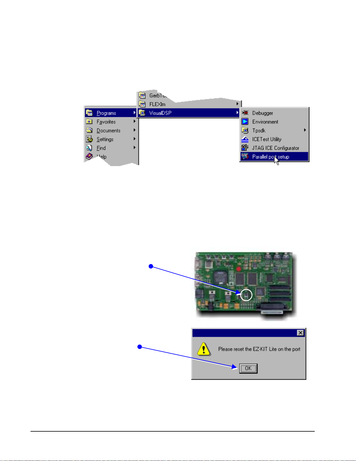
2.5.2. Parallel Port Setup
The ADSP-21160 EZ-KIT Lite includes a Parallel Port Setup utility to assist you in
establishing a communication path between the host PC and the ADSP-21160 EZ-KIT
Lite board. EPP mode is the preferred parallel port mode for the ADSP-21160 EZ-KIT
Lite. Bi-directional (PS/2 in some machines) mode is supported as an alternative. Use
this mode only if your parallel port controller does not include EPP mode support.
To configure the port correctly, you must
• Perform a BIOS Setup
• Run the Parallel Port Setup Utility
BIOS Setup
Use your host computer BIOS Setup utility to configure the parallel port. Refer to your
PC motherboard manual for more information. Use the following steps to set up your
host BIOS:
1. Shut down your computer.
2. Reboot your computer, and select the BIOS setup option.
3. In the BIOS setup screen, configure the parallel port for EPP mode.
For example, with a Phoenix BIOS, navigate to
Advanced > Integrated I/O Ports > Parallel Port
and set the port attributes to Auto configuration, EPP mode. (If your I/O port does
not support EPP mode, select bi-directional mode.)
4. Save the changes and reboot.
ADSP-21160 EZ-KIT Lite 13
Getting Started
Parallel Port
Setup Utility
To execute the Parallel Port Setup utility:
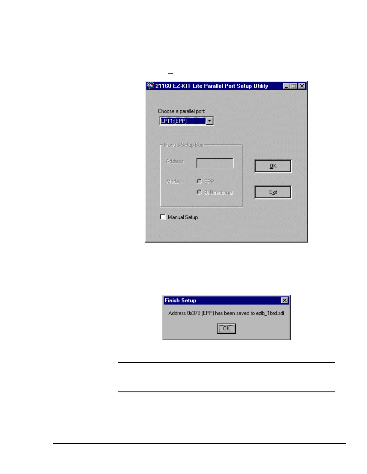
1. Connect the ADSP-21160 EZ-KIT Lite to a parallel port on the target PC.
2. Click Start > Programs > VisualDSP++ > Parallel port setup
The Parallel Port Setup utility polls at the default parallel port addresses 0x278 and
0x378. Ports responding as enhanced parallel port (EPP) compatible are tested for the
presence of an ADSP-21160 EZ-KIT Lite board.
The test is performed by writing a loop-back test message to each compatible port. The
resident monitor on the ADSP-21160 EZ-KIT Lite board responds to such messages by
echoing them back to the host. You must therefore first reset your ADSP-21160 EZ-KIT
Lite board to ensure it is properly initialized, and can respond to a poll request. To do so,
1. press the Master
Reset pushbutton on
the board,
2. wait for the board LEDs
to switch off, then click
OK.*
* You may need to wait for 5 seconds when using bi-directional mode on a slower
machine before clicking OK.
ADSP-21160 EZ-KIT Lite
14
Getting Started
The utility displays a screen listing the available EPP mode parallel ports. Select the port
from the list and click O
K to accept the parallel port setup information.
Manual Setup
The utility confirms the address information has been saved in a file in your <etc>
directory. The address information in this file is used by VisualDSP++ to establish a
communication path to the ADSP-21160 EZ-KIT Lite. Click OK to end the utility.
Note: If the parallel port is in bi-directional mode, the bracketed comments
(EPP) are replaced with (bi-directional), indicating the communication
protocol.
If the parallel port on your PC is not at either of the standard addresses (0x278 or 0x378),
use the Manual Setup option to specify its address and mode. When specified
manually, the utility does not poll the address you define. To validate the port you must
ADSP-21160 EZ-KIT Lite 15
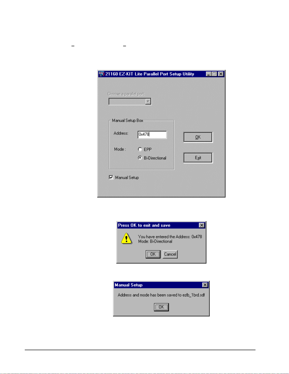
Getting Started
test the communication from the VisualDSP++ debugger. From the debugger window
Se
ttings menu, select Test Communications.
When entering the address, use hexadecimal notation as shown below. (for example,
enter ‘0x478’ rather than just ‘478’).
Enter the parallel port address and mode specification, and Click OK. To confirm the
values click OK, or Cancel to return to the setup screen to modify them.
Click OK to end the utility.
If you happen to corrupt the System Definition File (SDF), an original copy is available
on the Installation CD under the Original Files folder.
ADSP-21160 EZ-KIT Lite
16
Demonstration Programs
3 Demonstration Programs
3.1. Overview
This chapter describes loading and running the demonstration programs supplied with
the ADSP-21160 EZ-KIT Lite board. The demos are designed to run on the
VisualDSP++ debugger, which is supplied on the CD-ROM that shipped with this
product. For detailed information on debugger features and operation, see the
VisualDSP++ debugger Guide & Reference.
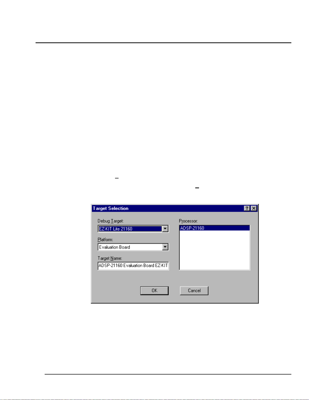
3.2. Starting the VisualDSP++ Debugger
After the VisualDSP++ software has been installed, you can start the VisualDSP++
debugger.
1. Click the Windows Start menu.
2. Select P
3. From the VisualDSP++ debugger window S
4. Configure the debug session as shown in the following figure, and click OK.
rograms >>>> VisualDSP++ >>>> Debugger.
ession menu, select New Session.
3.3. Debugger Operation with the ADSP-21160 EZ-KIT Lite
The VisualDSP++ debugger Guide & Reference contains most of the information you
will need to operate the VisualDSP++ debugger with your ADSP-21160 EZ-KIT Lite
board.
ADSP-21160 EZ-KIT Lite 17
Demonstration Programs
3.3.1. Loading and Running Programs
To load and run a demonstration program:
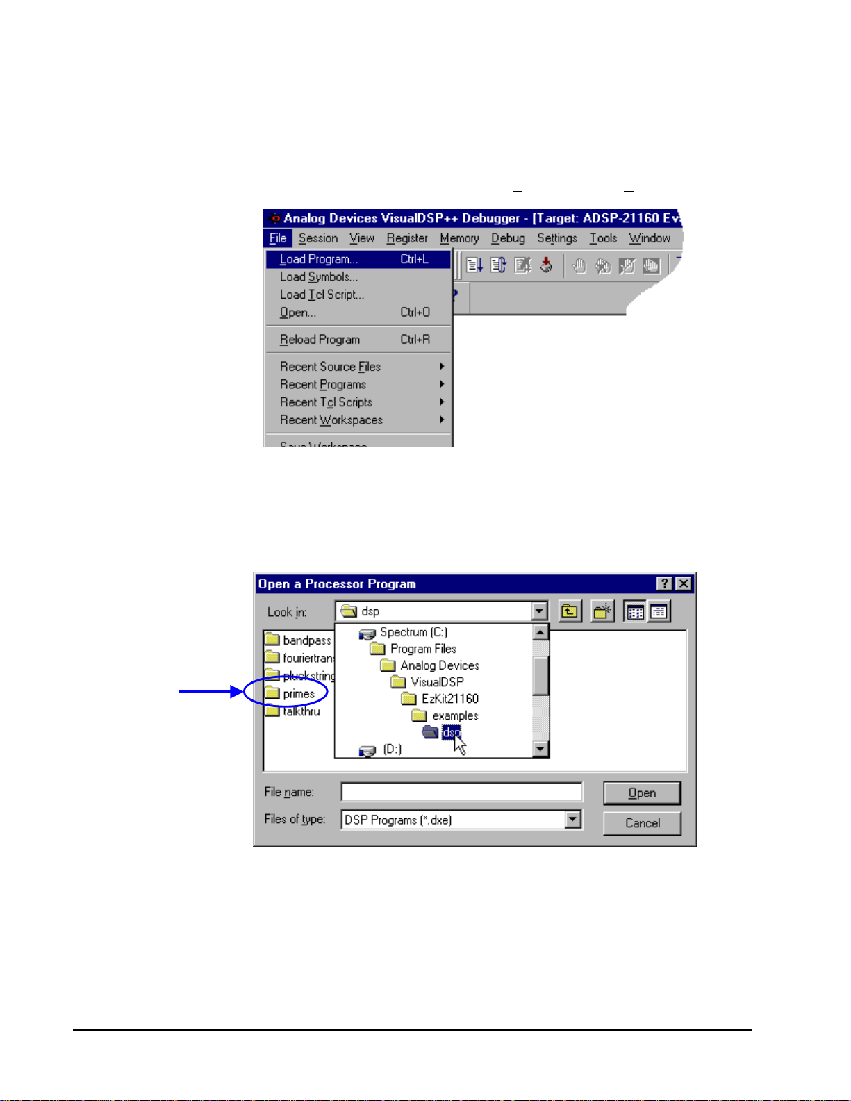
1. From the VisualDSP++ debugger window F
ile menu, select Load.
2. Navigate to the directory containing the demonstration program. (Demonstration
programs are installed in directories under <EzKit21160>\examples\dsp\
<demo name>\debug where <EzKit21160> is the root directory where you
installed the ADSP-21160 EZ-KIT Lite software and <demo name> is the
name of the demonstration program.)
ADSP-21160 EZ-KIT Lite
18
Demonstration Programs
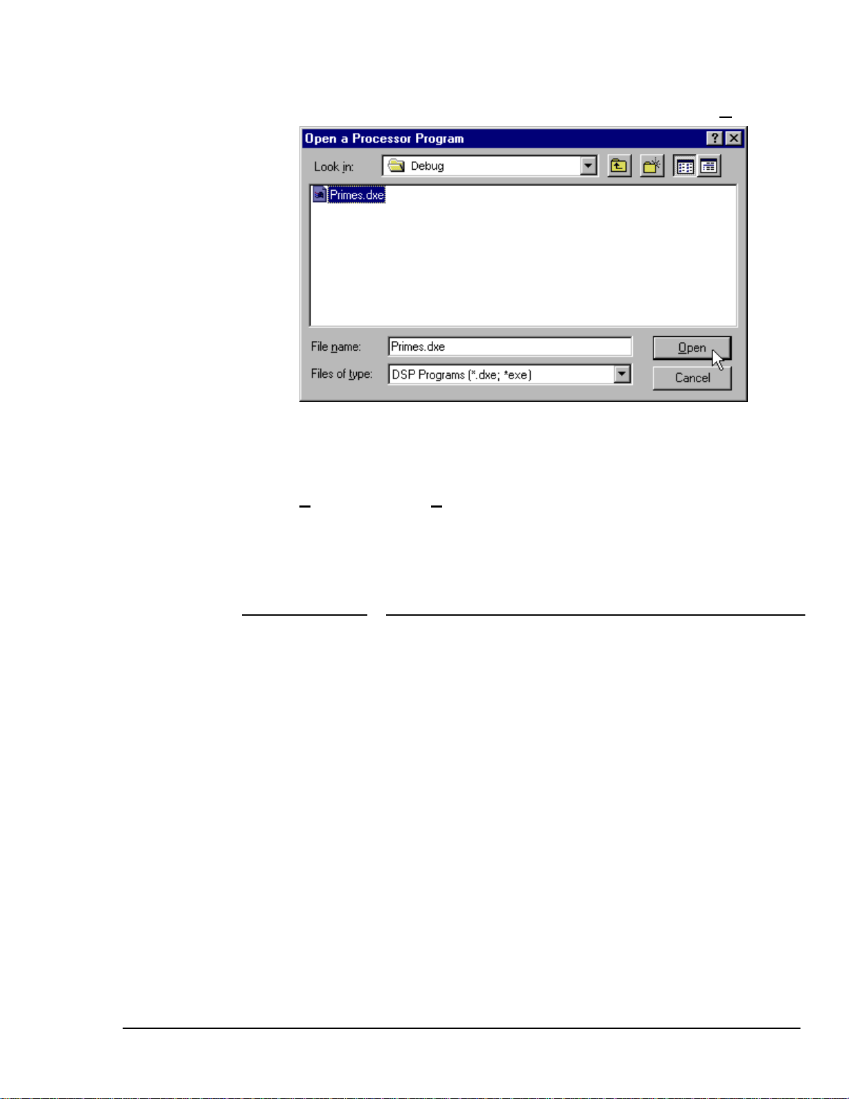
3. Select the executable file for the program (extension .dxe) and click Open
4. Wait for the “Load Complete.” message to appear in the Output window
before you attempt any debug activities.
5. To run the program, use the F5 key, or from the VisualDSP++ debugger window
D
ebug menu, select Run.
The VisualDSP++ debugger includes two commands useful for synchronization of your
test code and the resident monitor on the ADSP-21160 EZ-KIT Lite board. Observe the
following rules when using these commands
Command Usage and impact
Debug > Reset
Debug > Restart
Use to reset the board and reload the monitor executive.
Downloaded programs are lost in their entirety and must be
reloaded. POST routines are executed.
Use to restart the monitor executive after a Halt command or the
normal end of execution of a program. The monitor restarts
unambiguously at its main entry point, but retains information
about breakpoints and downloaded code. For programs which run
to normal completion, and which you wish to re-execute, this is
mandatory (Normal program completion halts at a breakpoint
placed over an idle instruction in the monitor. Continuing from this
point causes the monitor to idle forever.)
ADSP-21160 EZ-KIT Lite 19

Demonstration Programs
3.3.2. Registers and Memory
To see current values in registers, use the Register command and its subcommands to
select specific register groupings (I
To view the current contents of memory, use either the View > Debug Windows >
Plot command for a graphical view, or the Memory > Dump command for an ASCII
display. To modify memory values, use the Memory > Fill command. These functions
are operable only when the DSP program is paused (at a break point).
The F12 key or the Window >>>> Refresh command refreshes all current display
windows.
OP or Core) or your own Custom set of registers.
ADSP-21160 EZ-KIT Lite
20
Demonstration Programs
3.3.3. Resetting the Board
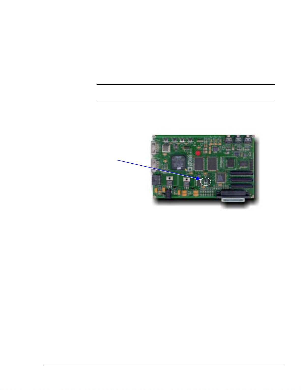
The ADSP-21160 EZ-KIT Lite board can be reset with the master reset push button
(RESET PB) on the board, or with the Debug > Reset command in the debugger.
Both resets clear and reset the ADSP-21160 EZ-KIT Lite board. Following a reset, you
will need to reload any programs you were running.
Note: Using the Master Reset pushbutton while running the debugger will
cause the host to lose communication with the board.
Master Reset Pushbutton
Figure 5 Master Reset Pushbutton
3.4. Demonstration Programs
The demonstration programs included with the ADSP-21160 EZ-KIT Lite are designed
to show you the features and capabilities of the VisualDSP++ debugger and the
ADSP-21160 DSP. The demos are listed by their executable file name and are described
by their output.
The demonstration program's executable code must be loaded first into the VisualDSP++
debugger before you can perform debug functionality within the debugger.
ADSP-21160 EZ-KIT Lite 21
Demonstration Programs
3.4.1. Fft.dxe
The FFT demo performs a frequency analysis on an analog signal presented to the board.
The program runs continuously, repeatedly acquiring a block of 128 samples from the
Codec, optionally filtering the input samples, applying the FFT and optionally scaling
the results. A demo control panel lets you vary these parameters at run-time. To view the
results you must set a break point in the program. (Data viewing and plotting is not
possible while the program is executing).
To configure your board, and run this demo, use the following procedure.
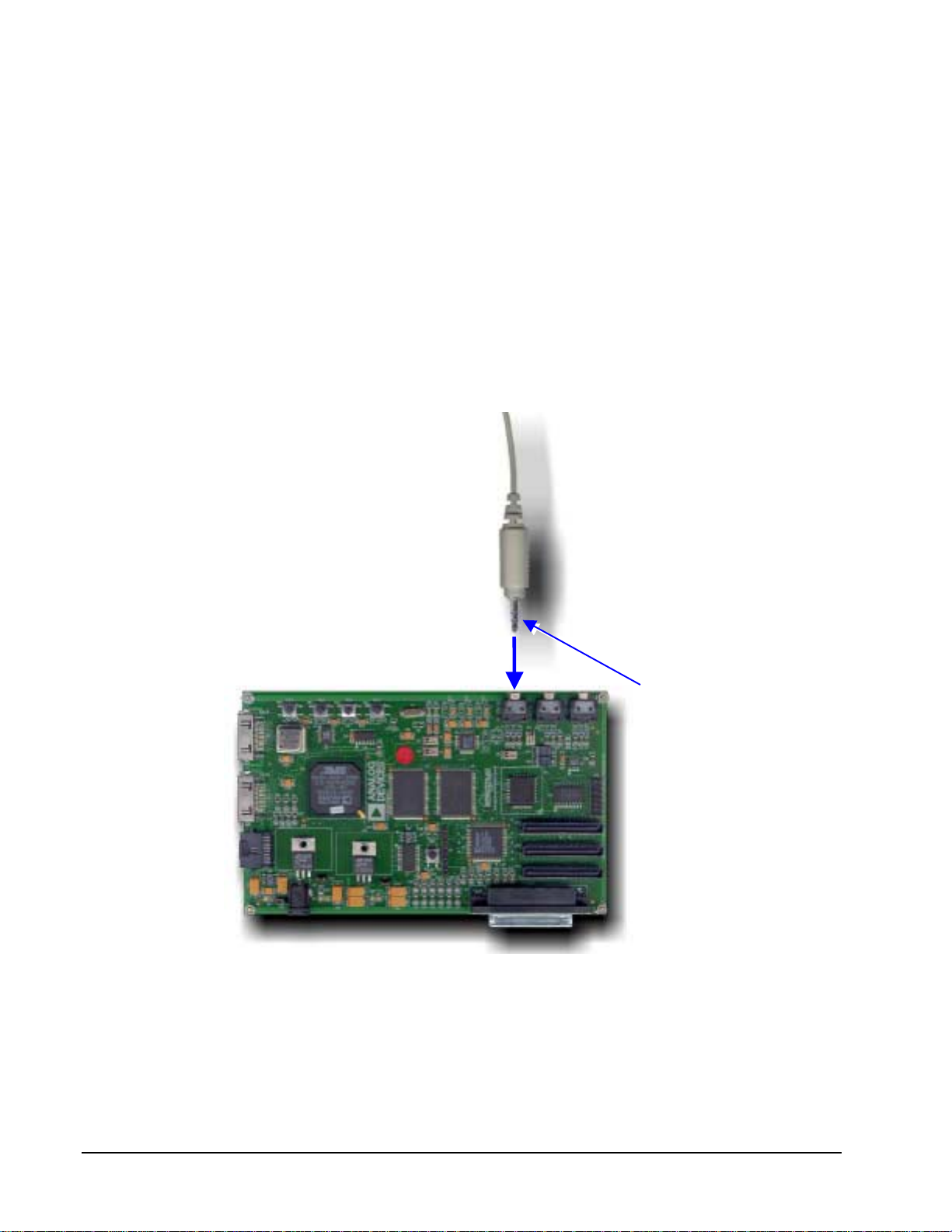
1. Connect the “Line Out” of an electronic audio device (or microphone) to
connector J6 (Line In) on the board.
Figure 6 FFT Example Board Setup
1. “Line Out” from audio device
2. Load the FFT example program
<EzKit21160>\examples\dsp\fouriertransform\debug\Fft.dxe
ADSP-21160 EZ-KIT Lite
22

Demonstration Programs
3. Set a breakpoint in the source code module Fft.c at the sample_codec();
statement. (Click on the source code line in the source code window, then click
the Toggle Break button in the VisualDSP++ menu bar). An asterisk appears
in column one of the source code line, indicating a break point at that location.
4. Start the Fft example by pressing the F5 key, or clicking D
ebug > Run on the
menu bar. The program begins execution, runs to the break point, and halts.
Once a breakpoint halt message is displayed, click OK.
ADSP-21160 EZ-KIT Lite 23

Demonstration Programs
5. From the menu bar, select View > Debug Windows > Plot and configure
four windows to view the source data and the FFT results. In the Plot
Configuration dialog window, ensure the parameters, other than A
ddress, are
defined as illustrated below.
6. For each plot, click B
region to plot (the A
Click Add and then OK to bring up the chosen Plot Window.
FFT Source Data (DataIn)
Imaginary component (ImDataOut)
Real Component (ReDataOut)
Magnitude (data)
rowse to view the symbol table and select a named data
ddress); DataIn, ImDataOut, ReDataOut or data.
ADSP-21160 EZ-KIT Lite
24

Demonstration Programs
7. Run the program from the breakpoint (F5 key). When the code halts again at the
breakpoint, click OK. The plot windows will be refreshed showing the most
recent sample data and its FFT results.
Input Data Plot
Real Component Plot
Imaginary Component Plot
Magnitude Plot
ADSP-21160 EZ-KIT Lite 25

Demonstration Programs
The FFT example includes a Demo control panel activated by the
Demo > Demo Control command. Radio buttons on this panel allow you to select
• the data source (Codec, Noise or Sine wave),
• the data domain (frequency or time),
• the data window filtering (none, Hamming or Blackman),
• and output data scaling (logarithmic or linear).
The Hamming or Blackman filter is applied only if the frequency domain is selected.
Both filters modify the sampled data by applying a positional dependant weighting
multiplier to each of the N (128) data samples.
Filter Weight Notes
Hamming 0.54 - 0.46 cos ( 2k*π / (N-1) ) k = sample
Blackman 0.42 - 0.5 cos ( 2k*π / (N-1) ) + 0.08 cos ( 4k*π / (N-1) ) N = total samples
The FFT demo is capable of generating (internally) a modulated sine wave as the data
source. If you do not have a clean external signal source to present to the Codec, you can
enable the internal generation by selecting Sine as the signal source on the Demo
Control pane.
ADSP-21160 EZ-KIT Lite
26
number

Demonstration Programs
3.4.2. BP.dxe
The BP demo modifies a signal by subjecting it to a band-pass filter. Configure the board
as illustrated in the following figure.
1. Speakers or Headphones
2. Source from audio device
Figure 7 Band Pass (BP) Example Board Setup
The Band pass example program includes a demo control panel activated by the Demo
> Demo Control command. Radio buttons on this panel allow you to select:
• the input source (Codec or internally generated noise)
• the filter range for the program
You can only select the input source (Codec/Noise) before running the program. If you
select Codec as the input source, the program will run in an infinite loop and you may
change the filter range at any time, even while the program is executing. If you select
Noise as the input source, the program will run and then terminate and you should only
set the filter range before the program runs.
ADSP-21160 EZ-KIT Lite 27

Demonstration Programs
While the program is running, you can also adjust the gain using the VisualDSP++
command Set
tings > Codec > Gain.
If you choose Noise, you can plot the generated noise input (NoiseIn) and the filtered
output (NoiseOut) once the program has terminated. Noise output is not sent to the
Codec.
ADSP-21160 EZ-KIT Lite
28

Demonstration Programs
3.4.3. Pluck.dxe
The pluck demo plays a tune (Stairway to Heaven) to the Line Out connector. To hear
the output, connect powered speakers or headphones to connector J9.
1. Speakers or Headphones
Figure 8 Pluck Example Board Setup
While the tune is playing, you can adjust the gain using the VisualDSP++ command
Settings > Codec > Gain. There is no Demo control panel associated with this
example.
ADSP-21160 EZ-KIT Lite 29

Demonstration Programs
3.4.4. Primes.dxe
The primes demo program calculates the first 20 prime numbers and sends them to the
VisualDSP++ debugger output window. There is no Demo control panel associated with
this example, or any required connector setup necessary.
ADSP-21160 EZ-KIT Lite
30

Demonstration Programs
3.4.5. Tt.dxe
The Talk-through demo samples data at 48 kHz from the Mic In of the CODEC (J1), and
then sends the data back out the Line Out of the CODEC (J9). To configure your board
for this demo, use the following procedure.
1. Plug a set of self-powered computer speakers (or headphones) into connector J9
(Line Out) on the board. Turn on the speakers and set the volume to an adequate
level.
2. Connect the “Line Out” of an electronic audio device (or microphone) to connector
J1 (Mic In) on the board.
Figure 9 Talk Thru Example Setup
1. Speaker output
2. Audio in
There is no Demo control panel associated with this example. You can, however, alter
the Codec gain while the example is running by using the Settings > Codec > Gain
command.
ADSP-21160 EZ-KIT Lite 31

Demonstration Programs
ADSP-21160 EZ-KIT Lite
32

Hardware Description
4 Hardware Description
At the heart of the ADSP-21160 EZ-KIT Lite board is the ADSP-21160 DSP processor.
Packaged on the board are a number of components, which interface to the DSP and
together constitute a small, effective demonstration system. The following sections
provide insight into the elements of the board, and describe:
• The processor and key core components
• The connectors on the board
• The functions of the push buttons and LEDs
• The configuration switches
• The user accessible test points
Use the information here, and in section 7, “Forming a Cluster”, to configure the board
as necessary for your use.
Caution: Always remove power from the board, and use static discharge
precautions, before modifying configuration switches, establishing or removing
test-monitoring equipment, connecting or disconnecting cables, or forming and
breaking a cluster configuration.
ADSP-21160 EZ-KIT Lite 33

Hardware Description
4.1. Processor and Core Components
Oscillators
Board (40 MHz)
CODEC (24.576 MHz )
CODEC
AD1881
Y1
X1
U2
U11
U4 U5
U8
U12
+5V Regulator
+3.3V Regulator
+2.5V Regulator
PLD
Flash Memory
ADSP-21160
U13
Power
U14
DSP Core
SBSRAM Memory
Figure 10 Core Component Locations
U6
4.1.1. Oscillators
Two oscillators are installed on the ADSP-21160 EZ-KIT Lite.
A 40 MHz oscillator provides board level clock signals for the DSP core and its
peripherals. The DSP core frequency is derived from this oscillator, and is scaled to a
maximum of 80 MHz.
A second oscillator (24.576 MHz) provides clock signals to the CODEC.
ADSP-21160 EZ-KIT Lite
34

Hardware Description
4.1.2. CODEC
The CODEC used on the ADSP-21160 EZ-KIT Lite board is the AD1881. The CODEC
interfaces to the processor using the SPORT1 serial channel
4.1.3. Power Supply
The ADSP-21160 EZ-KIT Lite uses three different power supply voltages: 5V, 3.3V and
2.5V. The estimated power requirements for the board are indicated in the following
table:
Device 5V 3.3V 2.5V
Processor 800mA 1000mA
SBSRAM x 2 600mA
CODEC 40mA 80mA
Analog 100mA
PLD 200mA
Flash 100mA
Other 200mA
TOTAL 340mA 1780mA 1000mA
All of the board power supplies are generated using linear regulators from an external
power supply module. The total current draw for the board is the sum of each of the three
supply currents. The total is approximately 3.12 Amps.
Power consumption on the ADSP-21160 EZ-KIT Lite was tested using software routines
to exercise different parts of the processor while measurements were made on each of the
power rails. The confirmed power draw during these tests are shown in the following
table:
ADSP-21160 EZ-KIT Lite 35

Hardware Description
Tests 2.5V Total 3.3V Total
Idle (no code after bootup) 330mA 230mA
Idle (JTAG halt) 60mA 390mA 0mA 230mA
Idle (main while(1)) 220mA 550mA 20mA 250mA
core A-5-A copy (internal-internal) 250mA 580mA 20mA 250mA
SPORT1 (48KHz) 210mA 540mA 20mA 250mA
SPORT0 (48KHz) 220mA 550mA 30mA 260mA
LP0-1 (max data rate) 260mA 590mA 30mA 260mA
LP2-3 (max data rate) 260mA 590mA 30mA 260mA
LP4-5 (max data rate) 270mA 600mA 50mA 280mA
LP0-5 (max data rate) 340mA 670mA 60mA 290mA
EP0 write (no burst) 300mA 630mA 140mA 370mA
EP1 read (no burst) 260mA 590mA 90mA 320mA
EP1 read (burst 4) 290mA 620mA 100mA 330mA
EP0 write & EP1 read (no burst) 300mA 630mA 140mA 370mA
EP0 write & EP1 read (w:nb – r:b4) 310mA 640mA 140mA 370mA
LP0-6, SP0-1, EP0-1, core (All at once) 390mA 720mA 80mA 310mA
*All tests involving read/write operations used a 0x100 array of memory.
Power is brought onto the board by a connector to the external power supply module.
The external power supply module (Baknor) provides a minimum of 2.1 Amps at 7.5
volts.
The 5V supply rail is regulated using an ADP3367 device (SO8 package). The 3.3V and
2.5V supplies use three-terminal linear regulators in TO220 packages, with heat-sinks
connected to the board GND plane. On-board power filtering is used to produce “quiet”
power and ground for the PLL of the ADSP-21160 processor.
When two ADSP-21160 EZ-KIT Lite are connected in a cluster an alternate external,
power supply module may be needed to meet the greater power requirements of the two
boards.
ADSP-21160 EZ-KIT Lite
36

Hardware Description
4.1.4. PLD
The PLD implements the state machines that run the parallel port interface. The PLD is a
Xilinx device in the XC95144QC100 family.
4.1.5. Flash Memory
The Flash memory on the ADSP-21160 EZ-KIT Lite is implemented using a single 8-bit
wide device (AMD). The device accommodates memory sizes of 1, 2, and 4 Mbit (all pin
compatible). The Flash memory is located in the “un-banked” area in the 21160 memory
map (In Boot Memory Select mode only).
The Flash memory also has an enable/disable switch (SW11) to allow two ADSP-21160
EZ-KIT Lite boards to be connected together in a cluster. When two boards are
clustered, the Flash memory must be disabled on one of them.
4.1.6. SBSRAM
The SBSRAM on the ADSP-21160 EZ-KIT Lite is implemented using two 64K x 32 bit
wide devices (Micron device). They interface to the upper and lower 32 bits of the 21160
external data bus (cluster bus). The SBSRAM occupies the external memory Bank 0
address space of the 21160 memory map (0x0080 0000 to 0x0081 FFFF).
The SBSRAM also has a pair of enable/disable switches (SW2 and SW10) to allow two
ADSP-21160 EZ-KIT Lite boards to be connected together in a cluster. When two
boards are clustered, the SBSRAM must be configured to prevent multiple mapping.
4.1.7. Processor
The ADSP-21160 EZ-KIT Lite boot mode, processor ID code, and processor clock ratio
are all user configurable. These functions are implemented using configuration switches
(SW11, SW10 and SW1) on the solder side of the ADSP-21160 EZ-KIT Lite. The
processor clock is generated from a socketed 40MHz oscillator.
ADSP-21160 EZ-KIT Lite 37

Hardware Description
4.2. Connectors
DSP Ports CODEC
Serial Port 1 (J21) Line In
Link Port 4 (J22) MIC In
Link P ort 5 (J23) Line Out
J1 J9J6
J23
J28
J22
JP4
J21
J26
Power Connectors
+7.5V supply JTAG
Cluster
Parallel Port
Figure 11 Connector Locations
JP6
JP5
J11
ADSP-21160 EZ-KIT Lite
38

Hardware Description
4.2.1. Serial Ports
The ADSP-21160 has two serial ports. Serial port 0 (SPORT0) is routed directly to a
shrouded, locking header (J21) to allow the user to connect it to other ADSP-21160 EZKIT Lite or external devices.
Serial port 1 (SPORT1) is routed to the on-board AD1881 CODEC. It provides a
data/control path between the CODEC and the ADSP-21160 processor.
Line In Stereo
Line Out Stereo
Mic In Mono
Serial Port 0
CODEC
AD 1881
Figure 12 Serial Port Routing
Serial Ports
0 1
ADSP 21160
Processor
S
ADSP-21160 EZ-KIT Lite 39

Hardware Description
4.2.2. Link Ports
The ADSP-21160 has six link ports. On the ADSP-21160 EZ-KIT Lite, two of the six
link ports are routed to connectors (link port 4 at connector J22, and link port 5 at
connector J23) and are available for external connection. The other four link ports are
interconnected on-board as loop-back pairs (link port 0 to link port 1,
link port 2 to link port 3).
ADSP 21160
Processor
S
Link Ports
Link Port 4
Link Port 5
0 1 2 3 54
Figure 13 Link Port Routing
4.2.3. Power Supply Connector
Power is brought onto the board by a connector (J26) to the external power supply
module. The external power supply module (Baknor) provides a minimum of 2.1 Amps
at 7.5 volts.
4.2.4. Audio Connectors
The Line level input (1/8th inch audio connector, J6) is connected to the 1881 CODEC
pins via a small passive filter/attenuation network to match the input levels to the
required levels for the CODEC.
th
The Mic input (1/8
inputs via AC coupling capacitors.
inch audio connector, J1) is routed directly to the 1881 CODEC
th
The Line level output (1/8
inch audio connector, J9) from the CODEC is routed via an
active filter network based on the SM2135S dual Op-Amp device, and terminated with a
47K Ohm load.
The input and output connectors have unpopulated connector sites connected in parallel
with the audio connectors. You can use these sites to wire external components to the
CODEC.
ADSP-21160 EZ-KIT Lite
40

Hardware Description
4.2.5. JTAG Connector
The ADSP-21160 EZ-KIT Lite is fitted with a standard JTAG emulator header (J28) for
debug interface to the ADSP-21160.
4.2.6. Cluster Connectors
The ADSP-21160 EZ-KIT Lite is able to operate in a cluster of two boards. To form a
cluster, stack two boards on top of each other using the PMC style connectors and
stand-offs (Connectors JP4, JP5 and JP6 on the component side; JP1, JP3 and JP7 on the
solder side).
The capacitive loading on the ADSP-21160 bus increases rapidly as boards are
connected. The cluster size is limited to two ADSP-21160 EZ-KIT Lite boards for full
speed bus operation.
The JTAG signals are routed to the cluster connectors to allow multi-processor JTAG
debug.
Caution: Do not attempt to stack more than two ADSP-21160 EZ-KIT Lite
boards. JTAG chaining will not function with more than two boards.
4.2.7. Parallel Port
The parallel port interface (J11) to the ADSP-21160 EZ-KIT Lite is implemented with
state machines in the PLD. The parallel port interfaces to the ADSP-21160 processor to
provide debug access for the user (via monitor software), and to the Flash memory to
allow the user to directly download boot code. The connection to the ADSP-21160 EZKIT Lite is via a standard IEEE 1284 connector.
The parallel port operates in EPP or bi-directional mode of the IEEE 1284 specification.
This provides 8-bit bi-directional communication to the host PC. The necessary
configuration cycles for the parallel port are implemented using state machines in the
PLD. The host PC acts as master for all cycles on the parallel port interface; the ADSP21160 EZ-KIT Lite board functions as a slave device. The “data” cycles (read and write)
of the EPP mode are used to communicate with the ADSP-21160, and the “address”
cycles communicate with the Flash memory.
The parallel port interface in the PLD also has an enable/disable switch to allow two
ADSP-21160 EZ-KIT Lite boards to be connected together in a cluster. The parallel port
interface must be disabled on one of the ADSP-21160 EZ-KIT Lite boards in a cluster.
ADSP-21160 EZ-KIT Lite 41

Hardware Description
4.3. Push Buttons / LEDs
Pushbuttons
Master Reset User LED’s
(PB0) Flag 3 LED
(PB1) Flag 2 LED
(PB2) Flag 1 LED
(PB3)
D3
D2 D1PB3 PB2 PB0PB1
RESET PB
D4
D5 D6
Power LED’s
+ 2 . 5 V o l t
+ 3 . 3 V o l t
+ 5 V o l t
Figure 14 Push Button and LED Locations
All four push buttons are de-bounced before being routed to the processor pins. PB0,
PB1, PB2 and PB3 correspond to IRQ0, IRQ1, IRQ2 and Flag 0 respectively. Two of the
interrupt lines to the processor (IRQ0 and IRQ1) are used to support the parallel port
interface and are not available as push button interrupts when the parallel port is enabled.
Three amber LEDs are connected to the Flag 1-3 pins of the processor with the processor
acting as the current sink. All user (amber) LEDs and push buttons have “not fitted”
headers connected in parallel to allow you to connect remote devices to these functions.
Each of the three power supplies on the ADSP-21160 EZ-KIT Lite has a green LED to
indicate when the supply rail is powered.
ADSP-21160 EZ-KIT Lite
42

Hardware Description
4.3.1. Master Reset Push Button (RESET PB)
The reset operation for the board is implemented using an ADM708 device. This device
provides Power-on and push button reset functions to the board.
Caution: Be careful not to depress the master reset push button too hard.
Applying excess pressure can cause the board to flex, damaging solder
connections.
The Master Reset pushbutton lets you initiate a power-on reset to the DSP. If you lose
contact between the ADSP-21160 EZ-KIT Lite board and your PC while running
programs, use the Master Reset button to restore communication.
Note: An active VisualDSP++ JTAG interface overrides a manual Master
reset.
4.3.2. User Push Buttons (PB0, PB1, PB2, PB3)
For user input/control, there are four pushbutton switches on the ADSP-21160 EZ-KIT
Lite board: IRQ0, IRQ1, IRQ2, and FLAG 0.
• The FLAG 0 pushbutton (PB3) toggles the status of flag pin FLAG 0 to the DSP.
• IRQ0, IRQ1 and IRQ2 correspond to the PB0, PB1 and PB2 pushbuttons.
• The IRQ pushbuttons let you send interrupts (IRQ’s 0, 1 and 2) to the DSP. This
manually causes interrupts when executing a program.
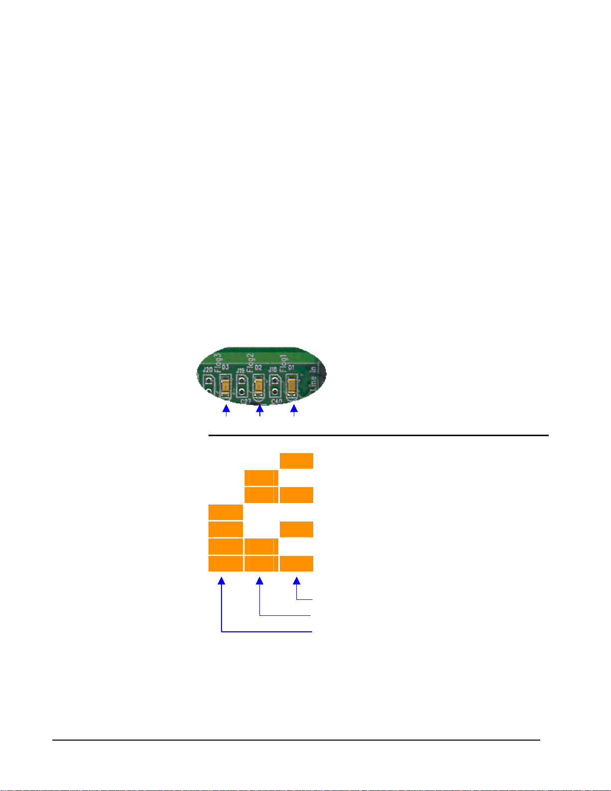
4.3.3. User LEDs (D1, D2, D3)
The user LEDs are tied directly to DSP FLAG pins 1, 2 and 3. User programs are free to
use these LED’s as visual feedback. Setting a FLAG pin to “1” illuminates its
corresponding LED.
FLAG Corresponding LED
1 D1
2 D2
3 D3
The POST routines also use the user LEDs to display test status during a reset. See
section 2.5.1. “Power-on Self Test (POST)” for details.
ADSP-21160 EZ-KIT Lite 43

Hardware Description
4.3.4. Power LEDs (D4, D5, D6)
The three green LED’s provide visual feedback for 5V power (D4), 3.3V power (D5) and
2.5 V power (D6). All three LED’s are calibrated to display the same brightness under
normal voltage conditions. A dimming of the intensity indicates a low-voltage supply.
The Power LEDs will often stay dimly lit when the board is disconnected from the power
supply. This is due to the power leakage through the processor silicon when the parallel
port or the JTAG connecters are left connected.
4.4. Configuration Switches
IRQ Routing (SW12)
FLAGS Routing (SW13)
Boot Mode (SW11)
Clock Configuration (SW9)
Clock Routing (SW1)
SW12 SW13
SW10 SW7 SW2
SBSRAM Configuration (SW2)
Button/Parallel Port (SW7)
JTAG/Board ID (SW10)
SW9 SW1 SW11
Figure 15 Configuration Switches
In addition to the configuration switches, the solder side also carries the other half of the
cluster expansion connectors, enabling two ADSP-21160 EZ-KIT Lite boards to be
stacked and form a cluster. The standoff legs provide clearance between two stacked
boards, preventing component contact.
ADSP-21160 EZ-KIT Lite
44

Hardware Description
The factory settings are:
• 40 MHz processor clock, enabled locally and distributed to the cluster bus
• All SBSRAM accessible
• Parallel port enabled in button mode with loop-back disabled
• The last board in the JTAG chain
• Set for booting from EPROM
• All IRQ and Flag signals isolated to the board
ADSP-21160 EZ-KIT Lite 45

Hardware Description
Table 1 Factory Settings - Configuration Switches
Factory Setting
Switch Function Positive Logic sense (On = True = 1) Pin Off On
SW1
SW2
SW7
SW9 Clock Ratio CLK/CFG0 1
SW10 Board ID LAST IN JTAG 1
SW11 Boot Mode EBOOT 1
SW12
SW13 FLAG Routing FLAG 0 ENABLED
Clock Routing Local Oscillator DISABLED 1
Cluster Clock = Local Clock
NOT USED
NOT USED
SBSRAM Configuration BR1 Pullup ENABLED 1
BR2 Pullup ENABLED
SBSRAM HIGH ENABLED
SBSRAM LOW ENABLED
Parallel Port Configuration Loop-back ENABLED 1
Parallel Port ENABLED
INTERRUPT DISABLED
NOT USED
CLK/CFG0
CLK/CFG0
CLK/CFG0
PROC ID 0
PROC ID 1
PROC ID 2
LBOOT
PROC/BMS = Cluster/BMS
FLSH/BMS = Cluster/BMS
IRQ Routing IRQ0 ENABLED 1
IRQ1 ENABLED
IRQ2 ENABLED
NOT USED
FLAG 1 ENABLED
FLAG 2 ENABLED
FLAG 3 ENABLED
2
3
4
2
3
4
2
3
4
2
3
4
2
3
4
2
3
4
2
3
4
1
2
3
4
!
!
!
!
!
!
!
!
!
!
!
!
!
!
!
!
!
!
!
!
!
!
!
!
!
!
!
!
!
!
!
!
If the ADSP-21160 EZ-KIT Lite board has the X1 crystal, EC13TS, then the SW1 pin 1
will DISABLE the board oscillator when turned ON.
If the board has the X1 crystal without the TS extension then SW1 pin 1 has no effect.
ADSP-21160 EZ-KIT Lite
46

Hardware Description
4.4.1. Clock Routing Switch (SW1)
The clock routing switch settings specify the clock source and its distribution on the
cluster bus when two ADSP-21160 EZ-KIT Lite boards are clustered together. Pin 1
enables or disables the local oscillator on the ADSP-21160 EZ-KIT Lite board. Pin 2
enables or disables the distribution of the local clock to the cluster bus. If the local
oscillator is disabled, the ADSP-21160 EZ-KIT Lite board uses the cluster bus clock
signal. If the local oscillator is enabled, the clock signal can also be distributed to the
cluster bus. In the factory default condition, the local oscillator is enabled, and
distributed to the cluster bus. Pins 3 and 4 are unused and must be left in the OFF
position.
4.4.2. SBSRAM Configuration Switch (SW2)
Each ADSP-21160 EZ-KIT Lite Board has 512 Kbytes of SBSRAM, configured in two
banks of 256Kbytes each. In a clustered environment, you must define how this memory
is accessed. Since both boards share the memory space, you must ensure that there is no
possibility of addressing two physical memory locations for any specific address. Pins 3
and 4 of SW2 determine whether a specific memory bank on a board is enabled. In a
single board configuration, both banks must be enabled (ON). In a two-board cluster, you
must ensure that each bank is enabled only once. For example, if you enable the low
memory bank (Pin 4 ON) on one board, you must disable the same bank (Pin 4 OFF) on
the other board.
Pins 1 and 2 define signal termination for multiprocessor bus request arbitration in a
clustered configuration. The ADSP-21160 EZ-KIT Lite uses only Bus Request lines 1
(BR1) and 2 (BR2) (maximum of two processors in a cluster). These pins must be set to
the “ON” position when a single board is used, and set to the “OFF” position when two
boards are clustered.
4.4.3. Parallel Port Configuration Switch (SW7)
Operation of the parallel port interface to the ADSP-21160 EZ-KIT Lite is controlled by
switch settings on the Parallel Port Configuration Switch (SW7).
The parallel port can be set into a diagnostic state using pin 1. In this state, data loops
back from both the PLD and the Host interface.
The parallel port can be effectively disabled on a board (for cluster operation) by
disabling the DSP interrupts using pin 3. Note that you should disable one of the boards
only, leaving the second board as the communication path for the parallel port connector.
ADSP-21160 EZ-KIT Lite 47

Hardware Description
4.4.4. Clock Configuration Switch (SW9)
The value defined by the Clock Configuration Switch settings specifies the multiplier
applied to the local oscillator to derive the core frequency of the DSP. The allowable
values for this setting are a function of the base frequency of the local oscillator, as
shown in the following table. Note that the maximum core frequency for the ADSP21160 EZ-KIT Lite is 80 MHz.
SW9 Pin Setting Clock ratio DSP Core Frequency (MHz)
0 1 2 3 25 33.3 40 50
1 1 1 1 n/a n/a n/a n/a n/a
0 1 1 1 n/a n/a n/a n/a n/a
1 0 1 1 2:1
0 0 1 1 3:1 75 100 n/a n/a
1 1 0 1 4:1 100 n/a n/a n/a
0 1 0 1 n/a n/a n/a n/a n/a
1 0 0 1 n/a n/a n/a n/a n/a
0 0 0 1 n/a n/a n/a n/a n/a
1 1 1 0 n/a n/a n/a n/a n/a
0 1 1 0 n/a n/a n/a n/a n/a
1 0 1 0 n/a n/a n/a n/a n/a
0 0 1 0 n/a n/a n/a n/a n/a
1 1 0 0 n/a n/a n/a n/a n/a
0 1 0 0 n/a n/a n/a n/a n/a
1 0 0 0 n/a n/a n/a n/a n/a
0 0 0 0 Reserved 25 33.3 40 50
Factory Default (1 = ON, 0 = OFF)
50 66.6
80
100
ADSP-21160 EZ-KIT Lite
48

Hardware Description
4.4.5. Board ID Switch (SW10)
Settings in the Board ID switch define both the ID of a board in a clustered
configuration, and the relative position of the board in a multi-board JTAG chain.
Pin 1 specifies the board position in a JTAG chain as either last (ON) or first (OFF).
Pins 2, 3 and 4 specify the ID of the board in a clustered configuration. For the ADSP21160 EZ-KIT Lite this ID must be either 001 (1) or 010(2). The ID corresponds to the
Bus Request line (BR) used by the board to arbitrate cluster bus accesses. Note that you
must also set pins 1 and 2 of switch SW2 (SBSRAM Configuration) appropriately. In a
cluster, these switches must be set to OFF (0); when used as a single board, both
switches must be ON (1). The following table illustrates the possible settings for these
switches.
SW10 SW2
Pins Pins Pins
23 4
1 1 1 Board ID = 0 x x 1 1
0 1 1 Board ID = 1 0 0 x x
1 0 1 Board ID = 2 0 0 x x
0 0 1 n/a x x x x
1 1 0 n/a x x x x
0 1 0 n/a x x x x
1 0 0 n/a x x x x
0 0 0 n/a x x x x
Factory Default (1=ON, 0=OFF)
When in a Cluster
1 2 Single Board 1 2
ADSP-21160 EZ-KIT Lite 49

Hardware Description
4.4.6. Boot Mode Switch (SW11)
The Boot Mode Switch pin settings specify the board’s boot mechanism. The factory
default setting selects Flash EPROM boot mode. The Flash EPROM is factory initialized
with the monitor executive program.
Note: If you are intending to use EZ-ICE JTAG, make sure to set the board to
Host boot or Link boot mode.
Pin
1 2 3 4 Boot Mode Selected
1 1 1 1 Host Booting
0 1 1 1 Boot from EPROM, BMS to cluster and Onboard Flash
1 0 1 1 Boot from Link Port
0 0 1 1 n/a
1 1 0 1 n/a
0 1 0 1 n/a
1 0 0 1 n/a
0 0 0 1 n/a
1 1 1 0 n/a
0 1 1 0 Boot from EPROM, Boot Memory Select to cluster bus
1 0 1 0 Boot from Link Port, Boot Memory Select to cluster bus
0 0 1 0 n/a
1 1 0 0 n/a
0 1 0 0 n/a
1 0 0 0 n/a
0 0 0 0 n/a
Factory Default (1=ON, 0=OFF)
4.4.7. IRQ Routing Switch (SW12)
The first three pins (1, 2, 3) of switch SW12 are used to direct the routing of IRQ signals
0, 1 and 2. When set to the ON position, the corresponding IRQ signal is connected to
the cluster bus, when OFF the signal is isolated to the specific board. In a single board
configuration the routing is irrelevant; in a clustered configuration, you must ensure that
routing is OFF on one board.
4.4.8. FLAG Routing Switch (SW13)
The four pins of switch SW13 are used to direct the routing of Flag signals 0, 1, 2 and 3.
When set to the ON position, the corresponding Flag signal is connected to the cluster
bus, when OFF the signal is isolated to the specific board. In a single board configuration
the routing is irrelevant.
ADSP-21160 EZ-KIT Lite
50

Hardware Description
4.5. Test Points
Push Button Take-off
Master Reset Mic In Mono
PB0 Line Out (Stereo)
PB1
PB2
PB3
Line In (Stereo)
J16
J24
J25
CODEC Signal Monitor/Insert
J12J13J15
J17
J27
J2 J7
J10
+5 V
+2.5 V
+3.3 V
Power Monitor
Figure 16 Test Points
The ADSP-21160 EZ-KIT Lite board, as illustrated above, has test points for
• Power,
• User push-buttons, and
• CODEC signals
The power test points allow you to place one or more ammeters in series to measure
current drawn by the board at each of the three voltages: 2.5 V, 3.3 V and 5 V. Jumpers
are factory installed at these locations.
ADSP-21160 EZ-KIT Lite 51

Hardware Description
Two pins are available at each push-button test point. You can connect a remote switch
across these pins.
Each of the three CODEC signal lines has three test point pins. You can inject signals at
these pins, or monitor the signals by tapping off the pins. Refer to the following diagram
for signal assignment.
RIGHT SIGNAL RIGHT
GND GND GND
LEFT SIGNAL LEFT
1 2 3
J7 (Line Out Stereo)
1 2 3
J2 (Mic In Mono) J10 (Line In Stereo)
1 2 3
Figure 17 CODEC Signal Pin Assignments
ADSP-21160 EZ-KIT Lite
52

Operation
5 Operation
5.1. Overview
The ADSP-21160 EZ-KIT Lite board and the monitor software are designed as targets
for the VisualDSP++ debugger. The debugger lets you view and modify processor
registers and memory, perform several debugging activities such as setting breakpoints,
stepping through code, and plotting a range of memory.
If you do not have the debugger installed on your system, you can install it from the
VisualDSP++ CD that came with this product. See “Software Installation” on page 11.
• This chapter provides you with monitor level software information that describes
how the ADSP-21160 EZ-KIT Lite board operates "out of the box". This chapter
also provides you with information to help you run your own programs on ADSP21160 EZ-KIT Lite Board.
This section covers the standard operation of the ADSP-21160 EZ-KIT Lite board. It
describes the I/O capabilities of the on-board components, board power-up, and the
on-board Monitor program.
5.2. Power-on Self Test (POST)
The ADSP-21160 EZ-KIT Lite factory installed EPROM includes a Power-on Self Test
procedure. The POST routines are executed whenever the ADSP-21160 EZ-KIT Lite is
powered on or reset. Test results are displayed through the amber user LED’s. A
successful POST sequence disables all three of the LED’s.
The POST routines test, in sequence:
• Internal RAM
• External SBSRAM
• Flash EPROM
• CODEC
For further information on which LEDs are affected by each test, refer to section 2.5.1.
ADSP-21160 EZ-KIT Lite 53

Operation
5.2.1. Flash EPROM
This test calculates and compares the Flash EPROM checksum.
• Read EPROM and calculate checksum.
• Compare calculated checksum with stored checksum in memory
5.2.2. External SBSRAM and Internal SRAM
To test the external SBSRAM and internal SRAM, the POST writes test patterns into the
memory and then reads the test pattern back for comparison. Three different test patterns
are used:
• Alternating one’s and zero’s. e.g. 101010101010….
• Alternating zero’s and one’s. e.g. 010101010101….
• Address as data. E.g. If the address is 0x200, then write 0x200 to that address.
5.2.3. CODEC
The POST tests the CODEC by writing to and reading from the CODEC’s registers. The
data written to the CODEC is pre-defined, and valid for the context of the register being
written to. A read from a register is expected to yield the same data written to it. This is a
test of the integrity of the path between the DSP and CODEC.
The test completes by generating a short tone. To hear the tone, connect headphones or
amplified speakers to J7. No LED is associated with the CODEC test.
5.3. Monitor Program Operation
The monitor program resides on the ADSP-21160 EZ-KIT Lite and provides the ability
to download, debug, and run user programs. The user interface for the monitor resides
on a Windows 95/98 or Windows NT host, which lets you operate the board remotely.
There are four main components of the monitor program:
• Halt Loop
• Parallel Port Host Write ISR
• Parallel Port Host Read ISR
• Command Processing Kernel
The monitor program idles in the Halt Loop when it is not running user code. In this
state, you can read/write memory, read/write registers, download programs, set
breakpoints, modify the CODEC configuration, and single step through code.
ADSP-21160 EZ-KIT Lite
54

Operation
To enter this state from your code, you must suspend or stop user code execution; either
with a breakpoint or a halt instruction. At this point, the host communicates with the
monitor, sending commands and reading data, via the Parallel Port. Commands from the
host are transmitted a single byte at a time.
Each byte written to the parallel port by the host generates an interrupt on the ADSP21160 EZ-KIT Lite. The ISR processing performed by the monitor reconstructs the
command byte by byte, and executes the Command Processing Kernel when a full
command packet has been received. The Command Processing Kernel then constructs
the corresponding response packet for the particular command and notifies the host
through the parallel port.
The host polls the parallel port’s status register to check for the command response from
the board. When a command response notification is detected, the host generates an
interrupt or a sequence of interrupts, which signals the monitor to transmit the response
packet to the host. When the entire response packet has been sent, the monitor returns to
its halt loop.
If the host sends a command to the ADSP-21160 EZ-KIT Lite while your user code is
running, the monitor processes the request in the same fashion. However, control is
returned back to the user code immediately after the interrupt is serviced.
The following restrictions should be followed to ensure correct board operation:
For a list of known restrictions when running programs using the Monitor Executive, see
section 6.6.
5.4. Interrupts
Each of the three external interrupts (IRQ0, IRQ1 and IRQ2) is directly accessible
through the pushbutton switches. IRQ0 and IRQ1 are used to implement interrupt driven
parallel port communication routines with the PC.
• Do not let a user program disable IRQ0/IRQ1 or change their corresponding
interrupt vector. The host loses contact with the monitor under this condition.
• Do not allow a user program to disable SPT1I or change the corresponding
interrupt vector. The host loses contact with the AD1881 CODEC.
• Do not design a user program which includes an ISR at a higher priority than
IRQ0. The host loses contact with the monitor.
Note: If you are intending to use EZ-ICE JTAG, make sure to set the board to
Host boot or Link boot mode.
The monitor executive running on the ADSP-21160 EZ-KIT Lite uses three interrupts
(IRQ0, IRQ1, and SPT1I) for normal operation. Avoid using these interrupts when the
monitor operation is needed. Interrupt vectors for these interrupts are provided in the file
ezlab21160_hdr.asm that comes with the ADSP-21160 EZ-KIT Lite. If these
vectors are overwritten, the kernel will not work as expected.
ADSP-21160 EZ-KIT Lite 55

Operation
Replaced Interrupt Vector Lost Functionality
IRQ0 Debugger’s ability to send a command to the board.
IRQ1 Debugger’s ability to read data from the board.
SPORT1 Interrupts Monitor’s ability to control AD1881 CODEC
Table 2 Interrupt Vector Assignment
The following rules and restrictions should be followed when using interrupts:
• All other interrupts, with the exception of IRQ0 and IRQ1 are masked-off when
the user program is halted.
• The board cannot communicate with the host if an interrupt higher than IRQ1 is
used.
• If you do not require the supplied monitor program, IRQ0, IRQ1, and SPT1I can
be configured for your own use. Replace the file ezlab21160_hdr.asm
with your own runtime header file. This removes all monitor and VisualDSP++
debugger functionality. To execute your program, you must use the EZFlash
utility (see section 6.4 “EZFlash programmer” for details) to write your code to
the FLASH memory. Your code will then execute the next time the board is
reset, or power is applied.
5.5. Breakpoints and Stepping
Breakpoints are used to stop the execution of code and examine processor registers and
memory when debugging code. You can insert your own breakpoints or single-step
through your code. To ensure proper monitor operation, adhere to the following
restrictions:
• Do not place breakpoints in the last 3 instructions of a do-loop.
• Do not set breakpoints in the branch determination phase following a delayed
branch instruction.
The VisualDSP++ debugger handles placement of breakpoints for stepping functionality.
Note: A DO loop that contains 4 instructions in length or less is stepped over.
5.6. Hardware Stacks
The hardware stacks in the ADSP-21160 can be accessed by using the Register> Core
> Stacks selection from the VisualDSP++ debugger menu. The stack view does not
provide transparency of the monitor executive. The PC Stack will always have a
minimum of two locations stored in a main user routine. These two addresses are used
by the monitor to:
ADSP-21160 EZ-KIT Lite
56

Operation
• store the return address from the monitor ISR
• and record the next code location of the current halt/breakpoint.
If the PC Stack is read in a user routine invoked by a “CALL” instruction, the return
address of that routine will be the third item on the stack. In this case the user program
PC stack usage begins at the third location. Since the monitor uses some PC Stack
locations, only 27 are available to the user program. See restrictions on the monitor in
section 6.6.
The Status Stack is also affected by the monitor executive. This stack will always
show a set of values even when the user program does not push anything into the stack.
If the user program does store values into the stack, the values will be shown as the
second down on the list. Because of this behavior, only 4 locations are available to the
user program. See restrictions on the monitor in section 6.6.
5.7. Benchmarking Utilities
The VisualDSP++ debugger provides two unsigned 32-bit cycle count registers to
measure the performance of DSP code execution between two breakpoints; the MS
(Most Significant) and LS (Least Significant) registers. These registers can be selected
from the Register > Core > Counters selection on the menu bar. The LS register is
incremented every cycle of user instruction executed. The MS is incremented when the
LS rolls over to zero.
Note: The MS register does not function correctly with the current revision of
this silicon. The counter is only accurate 232 –1 cycles, the number of cycles
which can be recorded by the LS register.
To use the counters, set both to zero at the start of the code segment. Place a breakpoint
at the end of the segment to be measured, or place the cursor over the segment end
instruction and choose Run To Cursor. The counter values show how many cycles
have elapsed for the code segment.
ADSP-21160 EZ-KIT Lite 57

Operation
ADSP-21160 EZ-KIT Lite
58

Programming Reference
6 Programming Reference
6.1. Memory Map
The ADSP-21160 memory space is divided into three sections:
• Internal memory space
• Multiprocessor memory space
• External memory space
Address Range Memory Section
0x0000 0000
0x000F FFFF
0x0010 0000
0x007F FFFF
0x0080 0000
0xFFFF FFFF
Internal Memory Space
Multiprocessor Memory Space
External Memory Space
Figure 18 ADSP-21160 Memory Addressing
ADSP-21160 EZ-KIT Lite 59

Programming Reference
The internal memory space is further divided into register space and multi-modal
memory space. Multi-modal memory space permits access to memory in three modes:
Long Word (64 bits), Normal Word (32 bits) or Short Word (16 bits). Memory
addressing is aliased in Blocks 0 and 1; the same physical location can be accessed in
any of the three modes as shown in the following diagram.
IOP Registers
Reserved
Block 0
Block 1
0x0000 0000
0x0000 00FF
0x0000 0100
0x0001 FFFF
0x0002 0000 0x0004 0000 0x0008 0000
0x0002 7FFF 0x0004 FFFF 0x0009 FFFF
0x0002 8000 0x0005 0000 0x000A 0000
0x0002 FFFF 0x0005 FFFF 0x000B FFFF
Reserved
0x0003 0000 0x0006 0000 0x000C 0000
0x0003 FFFF 0x0007 FFFF 0x000F FFFF
Long Normal Short
Address ranges for multi-modal access
Figure 19 ADSP-21160 Internal Memory Space
The memory map of the ADSP-21160 EZ-KIT Lite is laid out in the following table. All
shaded regions are reserved memory sections and required for the kernel to work
properly. Segment names for the reserved and user available regions are listed to the
right of the region.
ADSP-21160 EZ-KIT Lite
60

Programming Reference
IOP Registers
Reserved
Block 0
EZ-KIT monitor
(Reserved)
User Program
Code
0x0000 0000
0x0000 00FF
0x0000 0100
0x0001 FFFF
0x0002 0000
0x0002 00BF
0x0002 00C0
0x0002 017F
0x0002 0180
0x0002 0197
0x0002 0198
0x0002 01D3
0x0002 01D4
0x0002 0E3F
0x0002 0E40
0x0002 7FFF
0x0004 0000
0x0004 017F
0x0004 0180
0x0004 02FF
0x0004 0300
0x0004 032F
0x0004 0330
0x0004 03A7
0x0004 03A8
0x0004 1C7F
0x0004 1C80
0x0004 FFFF
0x0008 0000
0x0008 02FE
0x0008 0300
0x0008 05FE
0x0008 0300
0x0008 065E
0x0008 0660
0x0008 074E
0x0008 0750
0x0008 404F
0x0008 4050
0x0009 FFFF
seg_rth
(Interrupt vectors)
seg_init
(Monitor)
Monitor Host I/O
ISR’s
SPORT1 ISR
(Codec)
Monitor Code
seg_pmco
(User Code)
Block 1
User Data (PM)
User Data (DM)
Heap
EZ-KIT monitor
(Reserved)
Reserved
0x0002 8000
0x0002 8FFF
0x0002 9000
0x0005 D6FF
0x0002 D700
0x0002 E6FF
0x0002 E700
0x0002 F6FF
0x0002 F700
0x0002 FF7F
0x0002 FF80
0x0002 FFFF
0x0003 0000 0x0006 0000 0x000C 0000
0x0003 FFFF 0x0007 FFFF 0x000F FFFF
Long Normal Short
0x0005 0000
0x0005 1FFF
0x0005 2000
0x0005 ADFF
0x0005 AE00
0x0005 CDFF
0x0005 CE00
0x0005 EDFF
0x0005 EE00
0x0005 FEFF
0x0005 FF00
0x0005 FFFF
Figure 20 ADSP-21160 Memory Space Allocation
0x000A 0000
0x000A 3FFF
0x000A 4000
0x000A 5BFF
0x000B 5C00
0x000B 9BFF
0x000B 9C00
0x000B DBFF
0x000B DC00
0x000B FDFF
0x000B FE00
0x000B FFFF
seg_pmda
seg_dmda
seg_heap
seg_stak
Monitor data
memory
seg_ubuf
SPORT1 buffers
ADSP-21160 EZ-KIT Lite 61

Programming Reference
Note: External memory can not be used for Core Instruction Fetch (CIF).
48-bit/64-bit access to external memory fetches blocks that are 2 bits wide, making
consecutive even and odd memory fetches access the same memory space (for example,
0x800 000 and 0x800 001 are considered one memory space). Because of this, the user
can not run program code directly from external memory.
In addition, the VisualDSP++ debugger reserves the use of external memory area
(0x81FD00 – 0x81FFFF) to handle C-stdio instructions (printf, scanf, etc.).
6.2. Support Library
The ADSP-21160 EZ-KIT Lite includes a C-library for user control of
• the onboard AD1881 Codec,
• the user LEDs
The Codec library works only in conjunction with the resident monitor. It relies upon the
monitors internal serial port DMA buffering mechanism to receive data from and
transmit data to the Codec. The Codec data transfer functions are implemented as
blocking procedures. Specifically, control is not returned to the user until the requested
data has been transferred.
The onboard AD1881 CODEC is also accessible through the VisualDSP++ debugger
when the monitor executive is active. You can also set Codec parameters while example
programs are running with the monitor.
The following data structure (CODEC buffer) is required as an argument for the read and
transmit to codec registry:
31.. ..16 15.. ..0
Word 1
Word 2
Word 3
Word 4
Word 5
Unused AD1881 Tag
Unused AD1881 Command
Unused AD1881 Data
Unused Left PCM value
Unused Right PCM value
Only the least significant16 bits of each word are transmitted to or read from the
AD1881 CODEC. Refer to the AD1881 Codec Data Sheet for more information on the
CODEC operation, and the associated values for each word in the table.
ADSP-21160 EZ-KIT Lite
62

Programming Reference
SHARC_OpenSerPort1()
Function
Description
Include File
Syntax
Parameters
Returned Value
Remarks
See Also
Initializes serial port 1 (SPORT1) to work with the AD1881 Codec.
hhezl.h
RESULT SHARC_OpenSerPort1
UINT32
(
Flags);
Flags
unused
OK Normal completion
The function sets the SPORT1 in multi-channel mode and enables the monitor executive
DMA support for the Codec.
SHARC_CloseSerPort1()
ADSP-21160 EZ-KIT Lite 63

Programming Reference
SHARC_CloseSerPort1()
Function
Description
Include File
Syntax
Parameters
Returned Value
Remarks
See Also
Closes serial port 1 (SPORT1).
hhezl.h
RESULT SHARC_CloseSerPort1
UINT32
(
Flags);
Flags
unused
OK Normal completion
The function clears out initialization values for SPORT1 registers. All Codec functions
are disabled.
SHARC_OpenSerPort1()
ADSP-21160 EZ-KIT Lite
64

Programming Reference
HHEZL_SetupCodec()
Function
Description
Include File
Syntax
Parameters
Returned Value
Remarks
Initializes AD1881 Codec registers.
hhezl.h
RESULT HHEZL_SetupCodec
UINT32
(
Flags
unused
OK Normal completion
Sets the following default for the AD1881 CODEC operation:
Item Value
Serial configuration 16 bit
Master volume gain 0 dB
PCM volume gain 0 dB
Flags);
Serial Port access to the Codec must be active (prior call to SHARC_OpenSerPort1())
ADSP-21160 EZ-KIT Lite 65

Programming Reference
HHEZL_TransmitToCodec()
Function
Description
Include File
Syntax
Parameters
Returned Value
Remarks
Transmits serial data to AD1881 CODEC via Serial Port 1 transmitter (SPORT1Tx)
hhezl.h
void HHEZL_TransmitToCodec
UINT32 *
(
UserTxBuf);
UserTxBuf
User allocated 5 word CODEC transmit buffer
none
The content of UserTxBuf is copied for transfer to the AD1881 CODEC. The function
blocks until the buffer content is fully transferred to the monitor executives’ internal
DMA buffering mechanism.
Serial Port access to the Codec must be active (prior call to SHARC_OpenSerPort1())
ADSP-21160 EZ-KIT Lite
66

Programming Reference
HHEZL_TransmitReadToCodec()
Function
Description
Include File
Syntax
Parameters
Returned Value
Remarks
Writes and Reads from Codec Simultaneously
hhezl.h
void HHEZL_TransmitToCodec
UINT32 *
(
UINT32 *
UserTxBuf,
UserRxBuf);
UserTxBuf
UserRxBuf
User allocated 5 word CODEC transmit buffer
User allocated 5 word CODEC receive buffer
none
The content of UserTxBuf is copied for transfer to the AD1881 CODEC. The function
blocks until the buffer content is fully transferred to the monitor executives’ internal
DMA buffering mechanism, at which time the UserRxBuf is filled with the latest sample
from the Codec.
Serial Port access to the Codec must be active (prior call to SHARC_OpenSerPort1())
ADSP-21160 EZ-KIT Lite 67

Programming Reference
HHEZL_ReadFromCodec()
Function
Description
Include File
Syntax
Parameters
Returned Value
Remarks
Reads data from CODEC
hhezl.h
void HHEZL_ReadFromCodec
UINT32 *
(
UserRxBuf);
UserRxBuf
User allocated CODEC receive buffer (5 word buffer as described
above)
none
The function copies Codec data from Serial Port 1 Receiver (SPORT1Rx) into the user
allocated CODEC receive buffer. The function blocks until the data is transferred.
Serial Port access to the Codec must be active (prior call to SHARC_OpenSerPort1())
ADSP-21160 EZ-KIT Lite
68

Programming Reference
HHEZL_WriteCodecReg()
Function
Description
Include File
Syntax
Parameters
Returned Value
Remarks
Writes to CODEC
hhezl.h
void HHEZL_WriteCodecReg
UINT32
(
UINT32
RegOffset
Val);
RegOffSet
Val
Codec Register Offset
Value to write to the Codec Register
none
Internally this function constructs a 5 word CODEC buffer, placing RegOffSet in the
second word of the buffer (AD1881 Command) and Val in the third word of the buffer
(AD1881 Data). The function calls HHEZL_TransmitToCodec to perform the data
transfer.
See Also
Serial Port access to the Codec must be active (prior call to SHARC_OpenSerPort1())
HHEZL_TransmitToCodec()
ADSP-21160 EZ-KIT Lite 69

Programming Reference
SHARC_SetLed()
Function
Description
Include File
Syntax
Parameters
Sets the state of one or more LEDs accessible to the DSP.
hhezl.h
RESULT SHARC_SetLed
UINT32
(
UINT32
LedNum
The LEDs to set. LEDs are specified by the logical OR of any
combination of the following values (defined in def21160.h)
FLG1 (LED D1)
FLG2 (LED D2)
FLG3 (LED D3)
State
0 = turns the LED off
1 = turns the LED on
2 = flashes the LED at rate indicating OK status
5 = flashes the LED at rate indicating ERROR status
LedNum
State);
Returned Value
Remarks
OK Normal completion
This function does not return if either of states 2 or 5 is requested. Use State 2 or 5 only
under extreme or unrecoverable conditions.
ADSP-21160 EZ-KIT Lite
70

Programming Reference
6.3. Creating and Running Your Own Progr ams with VisualDSP++
This section provides basic information for creating and debugging your own program
using the ADSP-21160 EZ-KIT Lite board and the monitor executive.
For proper operation of the ADSP-21160 EZ-KIT Lite monitor you must include the
following components in your program:
• ezlab21160_hdr.doj
• ezlab21160.ldf
The file ezlab21160_hdr.doj replaces the default runtime header for the ADSP-21160
provided by the VisualDSP++ tools. This file should always be included in your project.
It defines the reset vector and interrupt vectors, which synchronize the user code with the
operation of the monitor executive.
The file ezlab21160.ldf is the default linker description file, which must be used to
properly place your program and data code if you intend to use the monitor. The
memory segments declared will not conflict with the memory space used by the monitor.
Consult the VisualDSP++ User’s Guide for more information on customizing the ldf
format. You can only change the non-reserved memory space.
Although there are many ways to go about developing programs in the VisualDSP++
environment, the example follows these steps:
1. Create a New Project File
2. Set Target Processor Project Options
3. Add and Edit Project Source Files
4. Customize Project Build Options
5. Build a Debug Version of the Project
6. Execute and Debug the Project
In this example you will create a new version of the Primes example which will
• Calculate the first 21 prime numbers
• Turn on LED one for every second prime number found
ADSP-21160 EZ-KIT Lite 71

Programming Reference
6.3.1. Create a New Project File
To create a new project file, go to the menu bar and click File > New > Project. The
VisualDSP++ environment will ask for a directory location for the new project file.
Choose <EzKit21160>\examples\dsp\primes for your project directory. Give the
new project the name primex.
6.3.2. Set Target Processor Project Options
VisualDSP++ prompts you for the project options. Under the Project tab, select ADSP21160 as the P
configuration setting is set to debug.
rocessor, and DSP Executable as the project Type. Ensure that the
ADSP-21160 EZ-KIT Lite
72

Programming Reference
6.3.3. Edit and Add Project Source Files
The primex project contains a single source file. To create this file, choose File > Open
and select the file Primes.c from the primes example directory.
ADSP-21160 EZ-KIT Lite 73

Programming Reference
Edit the file as shown in the shaded regions below.
additional include
statement for the
FLG definitions
extend array size
and iteration limit to
21 (force 20 prime
numbers)
add statement to
turn off all LED’s
before the loop
begins
add statement to
turn on the LED on
each odd-numbered
iteration, and turn
the LED off on evennumbered iterations
/* primes.c - calculate the first twenty prime numbers */
/* Analog Devices, 1993 */
unsigned int _PRIMES;
#include <stdio.h>
#include "def21160.h"
int _PRIMES;
int primes[21] = {2};
main()
{
int index = 0;
int n_primes = 1;
int testnum = 3;
/* turn off all LEDs */
SHARC_SetLed( FLG3|FLG2|FLG1, 0 );
/* print the first prime number */
printf (“%d\n”, primes[0]);
while (n_primes < 21)
{
/* find a number that is indivisible by known primes. */
while (index < n_primes)
if (!(testnum % primes[index++]))
{
/* if a number is divisible by a known prime, it
cannot be prime. Start over with the next
odd number */
testnum += 2;
index = 0;
}
/* turn on LED one for every second prime number */
SHARC_SetLed( FLG1, (n_primes % 2));
/* this number is prime, add it to the list. */
primes[n_primes++] = testnum;
printf("%d\n",testnum);
/* start checking at the next odd number */
testnum += 2;
index = 0;
}
}
ADSP-21160 EZ-KIT Lite
74

Programming Reference
When your edits are complete, chose File > Save As, and save the file as Primex.c. Use
the Project > Add to Project > File(s) command to add
• Primex.c
• <EzKit21160>\lib\hhezl_alib.dlb
• <EzKit21160>\etc\ezlab21160.ldf
• <EzKit21160>\etc\ezlab21160_hdr.doj
to your project. The project now has the following components and structure.
ADSP-21160 EZ-KIT Lite 75

Programming Reference
6.3.4. Customize Project Build Options
Before compiling the project, click Project > Project Options.. and ensure the
Generate debug information option is selected in the Compile tab.
6.3.5. Build a Debug Version of the Project
Select Project > Build Project from the VisualDSP++ Integrated Development
Environment menu bar. The project files are compiled assembled and linked to create the
executable file Primex.dxe.
6.3.6. Execute and Debug the Project
Start the VisualDSP++ debugger, load and run the Primex example. Observe that 21
prime numbers are calculated, and LED one flashes 10 times, staying in the unlit
condition when the example ends.
ADSP-21160 EZ-KIT Lite
76

Programming Reference
6.4. EZFlash programmer
The EZFlash utility is a DOS command line utility that accepts one command line
argument. The command line argument specifies:
*.ldr filename (contains data to write to flash )
A blank character separates all parameters.
Note: Make sure that you close the debugger before executing the EZFlash
utility.
To use the utility, first open a command window:
Start > Programs > Command Prompt
then in the command window, enter (for example)
EZFlash c:/flashcode/mycode.ldr
6.5. Creating Assembly Language Program
The following section will guide you on how to create your own assembly program and
debug it using the monitor.
The first thing to look at is the linker description file (LDF). The default linker
description file ezlab21160.ldf shows the reserved and non-reserved memory
sections. It is very important that you do not overwrite code in a reserved memory
section as this will corrupt the monitor.
Next, you need to setup the Interrupt Vectors in seg_rth section in the linker
description file. The monitor, by default, uses three interrupt vectors: IRQ0, IRQ1,
SPT1I.
SPT1I is only required for the codec library. You can replace this with your own custom
Interrupt Service Routine (ISR) if necessary but be aware that Codec access from the
debugger will not function properly if you do so. The following is the Monitor SPT1I:
#define Mon_SPT1I JUMP 0x40220;RTI;RTI;RTI
IRQ0 and IRQ1 are necessary for the operation of the monitor and should remain
unmodified. If you do need to place a jump to your own Interrupt Service Routine (ISR)
for a lower priority interrupt than IRQ0, make sure that IRQ1 and IRQ0 are both setup
correctly. The following definitions are required for the monitor.
#define Mon_IRQ1I JUMP 0x40200;RTI;RTI;RTI
#define Mon_IRQ0I JUMP 0x40210;RTI;RTI;RTI
ADSP-21160 EZ-KIT Lite 77

Programming Reference
In order for the debugger to halt at the starting point of your program code after a load,
you must name your main function _main. Make sure to check the Generate Debug
Information option in your Project Option > Assemble tab. There are restrictions
on creating assembly programs to work with the monitor, for details see section 6.6.
The following sections of example code demonstrate the previous concepts using the
LED D1(Flag1). You can build the code by including the default ezlab21160.ldf
into your project.
Example 1 – Non Interrupt Method
/*******************************************************************
File: FLG1flash.asm
Description: Assembly program example for EZ-KIT Lite 21160 using
********************************************************************/
#include "def21160.h"
#define Mon_SPT1I JUMP 0x40220;RTI;RTI;RTI
#define Mon_IRQ0I JUMP 0x40210;RTI;RTI;RTI
#define Mon_IRQ1I JUMP 0x40200;RTI;RTI;RTI
.GLOBAL _main;
/* Interrupt vectors */
.section/pm seg_rth;
Reserved_1:
nop; nop; nop; nop;
Chip_reset:
nop; jump _main; nop; nop;
/* Program code */
.section/pm seg_pmco;
_main:
BIT SET MODE2 FLG1O; /* Set FLG1 for output */
nop;
_toggle:
LCNTR = 1000 , DO loop1 UNTIL LCE; /* Loop for at least 125 ms */
loop1: nop;
monitor executive. The timing uses delay loop.
LCNTR = 2500, DO loop2 UNTIL LCE;
nop;
nop;
nop;
loop2: nop;
jump _toggle (DB); /* infinite loop flashing LED1 */
BIT TGL FLAGS FLG1;
nop;
/* Terminate and wait */
wait1: idle;
ADSP-21160 EZ-KIT Lite
78
jump wait1;

Programming Reference
Example 2 – Use Low priority timer interrupt
/*******************************************************************
File: FLG1flashint.asm
Description: Assembly program example for EZ-KIT Lite 21160 using
********************************************************************/
#include "def21160.h"
#define Mon_SPT1I JUMP 0x40220;RTI;RTI;RTI
#define Mon_IRQ0I JUMP 0x40210;RTI;RTI;RTI
#define Mon_IRQ1I JUMP 0x40200;RTI;RTI;RTI
#define UNUSED_INT nop; rti; rti; rti
#define RESERVED_INT nop; nop; nop; nop
#define T_PERIOD 10000000
.GLOBAL _main;
/* Interrupt vectors */
.section/pm seg_rth;
Reserved_1:
nop; nop; nop; nop;
Chip_reset:
nop; jump _main; nop; nop;
_IICDI: UNUSED_INT;
_SOVFI: UNUSED_INT; /* status/loop/PC stack overflow */
_TMZHI: UNUSED_INT; /* high priority timer */
_VIRPTI: UNUSED_INT; /* external interrupts */
_IRQ2I: UNUSED_INT;
/***********************************************************************
IRQ1 is the monitor's host read interrupt. If the user overwrites this,
then parallel port communication from DSP to Host will break.
***********************************************************************/
_IRQ1I: Mon_IRQ1I;
/***********************************************************************
IRQ0 is the monitor's host write interrupt. If the user overwrites this,
then parallel port communication from Host to DSP will break.
***********************************************************************/
_IRQ0I: Mon_IRQ0I;
_SPR0I: UNUSED_INT; /* serial port DMA channel interrupts*/
_SPR1I: UNUSED_INT;
_SPT0I: UNUSED_INT;
/************************************************************************
SPT1I is the monitor's CODEC Sport interrupt. The user can only overwrites this with the supported library function, so the host can set
CODEC registers.
************************************************************************/
_SPT1I: Mon_SPT1I;
_LP0I: UNUSED_INT; /* link port DMA channel 4 */
_LP1I: UNUSED_INT; /* link port DMA channel 5 */
_LP2I: UNUSED_INT; /* link port DMA channel interrupts */
_LP3I: UNUSED_INT;
_LP4I: UNUSED_INT; /* link port DMA channel 8 */
_LP5I: UNUSED_INT; /* link port DMA channel 9 */
_EP0I: UNUSED_INT; /* ext port DMA channel interrupts */
_EP1I: UNUSED_INT;
_EP2I: UNUSED_INT;
monitor executive. The timing uses timer interrupt.
RESERVED_INT;
ADSP-21160 EZ-KIT Lite 79

Programming Reference
_EP3I: UNUSED_INT;
_LSRQI: UNUSED_INT; /* link service request */
_CB7I: UNUSED_INT; /* circular buffer #7 overflow */
_CB15I: UNUSED_INT; /* circular buffer #15 overflow */
_TMZLI:
/* Program code */
.section/pm seg_pmco;
_main:
BIT SET MODE1 NESTM|IRPTEN; /* Nesting and global int enable */
BIT SET MODE2 FLG1O; /* Set FLG1 for output */
BIT CLR MODE2 TIMEN;
nop;
tperiod = T_PERIOD;
tcount = T_PERIOD;
BIT SET IMASK TMZLI;
BIT SET MODE2 TIMEN; /* Enable timer */
/* wait forever */
wait1:
nop;
nop;
jump wait1;
jump _isr_timer; /* low priority timer */
rti;
nop;
nop;
_isr_timer:
BIT TGL FLAGS FLG1;
_isr_timer:
BIT TGL FLAGS FLG1;
RTI;
ADSP-21160 EZ-KIT Lite
80

Programming Reference
6.6. Restrictions on Using the Monitor Executive
When running code using the Monitor Program there are certain registers and
instructions that must be used with caution. The following table contains a list of
restrictions that must be observed when writing programs intended for use with the
Monitor Program.
Table 3 Known Restrictions with the Monitor Program
Affected register/
Monitor reset value Description
instruction
SYSCON 0x00414000 IMDW1 must be cleared (only 32-bit
access is allowed to memory bank 1).
MSIZE must be set to 0100.
MODE1 0x00011800 Global interrupt must be enabled.
Nested interrupt must be enabled.
MODE2 0x40070010 Use level-sensitive interrupts.
Cache must be disabled for stepping.
Set FLG0 (PB3) – input; FLG1,2,3 –
output
WAIT 0x01CE1385 Do not change this value.
PCSTK N/A Only 27 locations available to the user.
DO LOOP N/A Less than 4 instruction-lengths are
stepped over.
Do not set breakpoints within 3
instructions from the end of the loop.
6 Nested loops are allowed, but no
Codec access from the host inside the
th
loop.
6
Status Stack N/A 4 locations are available to the user.
Effect Latency N/A Instructions which take advantage of
effect latency are not allowed (execute
improperly when stepped).
IMASK 0x000081C2 IRQ0 and IRQ1 must be unmasked.
Higher Priority
Interrupts
Delayed Branch N/A Do not set breakpoints on the two
N/A Interrupts higher than IRQ1 cannot be
debugged.
instructions following a delayed branch
(DB).
ADSP-21160 EZ-KIT Lite 81

Programming Reference
ADSP-21160 EZ-KIT Lite
82

Forming a Cluster
7 Forming a Cluster
Two ADSP-21160 EZ-KIT Lite boards can be connected to form a cluster by stacking
and connecting with the cluster connectors. To do so:
1. Remove power connections from all boards
2. Disconnect parallel port connectors
3. On both boards, set the configuration switches for your requirements.
4. Stack boards to form a cluster; Important: Remove nuts from the lower board and
screw the lower board to the upper board legs to provide mechanical support. Do not
stack both boards without using the proper board legs.
5. Connect the parallel port cable (to upper board only)
6. Connect power (to upper board only)
Note: Only a 2 board-cluster is supported. When two ADSP-21160 EZ-KIT
Lite are connected in a cluster an alternate external, power supply module may
be needed to meet the greater power requirements of the two boards.
Multiprocessing Debug is only available using the ICE-Emulator. The Parallel Port does
not support this feature. As an alternative, you can use the EZFlash utility (see section
6.4 above) to program the Flash ROM with your multiprocessing code via the parallel
port.
7.1. Signal Routing i n a Cl uster
The cluster connectors on the ADSP-21160 EZ-KIT Lite provide a signal bridge for
inter-board communication. Specific signal lines are grouped and assigned to carry:
• 32 memory address lines
• 64 data lines
• 4 Flag lines (0, 1, 2 and 3)
• 3 IRQ signals (0, 1 and 2)
• 1 system clock line
• JTAG signals
• Cluster signals
Since these signals are shared and accessible by both ADSP-21160 EZ-KIT Lite boards
in a cluster, you must configure each board, using the configuration switches, to specify
which board controls which signals. Specifically, you must:
ADSP-21160 EZ-KIT Lite 83

Forming a Cluster
• Provide each board with a unique ID
• Configure which board’s memory is used (memory space is common)
• Choose which board provides the system clock
• Select which board terminates the JTAG chain
• Select which board controls the Flag lines (and therefore responds to the pushbutton
interrupts)
• Define which board handles the IRQ lines
• Choose which board controls the parallel port
When selecting board functionality, remember that only the top board in a cluster
provides easy access to the pushbuttons, and unrestricted space to connect a JTAG pod.
For this reason it is advisable to configure the upper board to handle the FLAG and IRQ
lines, and assign the bottom board as the last board in the JTAG chain.
7.2. Example Cluster Configuration
Use the following example as a guideline for configuring a cluster. Each step illustrates a
cluster requirement to be met, and the configuration switch settings made to meet that
requirement. The example illustrates a typical cluster, where the top board will handle
the parallel port, respond to the push buttons, and provide the physical connection to the
JTAG chain.
7.2.1. Identify the Boards and their JTAG positions
In an ADSP-21160 EZ-KIT Lite cluster, the upper board must have the board ID1
(binary 001) and the bottom board must be ID2 (binary 010). The upper board must
also be configured as the first board in the JTAG chain and the lower board as the last in
the JTAG chain. The JTAG cable will be attached to the header on the upper board.
Lower Board Upper Board
Pin Off On Pin Off On
1
2
3
4
!
!
!
PROC ID BIT1
!
SW10 Board ID
LAST IN JTAG
PROC ID BIT0
PROC ID BIT2
1
2
3
4
!
!
!
!
7.2.2. Configure SBSRAM allocation
The two banks of SBSRAM memory on the each board in a cluster shares the same
memory space as the two banks on the other board. For this example, the lower board
provides one bank (upper half) of memory; the upper board provides the other (lower
half) bank. This demonstrates that, from the perspective of the cluster bus, it is irrelevant
where the memory is physically located as long as only one bank each of lower and
upper memory is enabled.
ADSP-21160 EZ-KIT Lite
84

Forming a Cluster
In a cluster configuration, the board ID controls bus arbitration. Bus Request lines BR1
and BR2 must therefore be allowed to be driven by the two processors in the cluster
(OFF). The upper board (board ID 1) uses BR1, the lower board uses BR2. In a single
board configuration, BR1 and BR2 must be enabled (ON).
Lower Board Upper Board
Pin Off On Pin Off On
1
2
3
4
!
!
!
BR1 Pullup ENABLED
BR2 Pullup ENABLED
!
SBSRAM LOW ENABLED
SW2 SBSRAM Configuration
SBSRAM HIGH ENABLED
1
2
3
4
!
!
!
!
7.2.3. Select the clock sources and multipliers
For the example cluster, the local oscillator on the upper board is enabled and distributed
to the cluster bus. The lower board has its local oscillator disabled and therefore uses the
cluster clock signal generated by the upper board. The clock configuration, SW9, settings
must be the same for both the upper and lower board.
The example illustrates a clock ratio setting of 2:1 (SW9). Assuming a 40MHz local
oscillator on the upper board, this sets the operating frequency of both boards at 80 MHz.
Lower Board Upper Board
Pin Off On Pin Off On
1
2
3
4
1
2
3
4
!
!
!
!
!
Cluster Clock = Local Clock
!
CLK/CFG1
!
!
SW1 Clock Routing
Oscillator DISABLED
NOT USED
NOT USED
SW9 Clock Configuration
CLK/CFG0
CLK/CFG2
CLK/CFG3
1
2
3
4
1
2
3
4
!
!
!
!
!
!
!
!
If the ADSP-21160 EZ-KIT Lite board has the X1 crystal, EC13TS, then SW1 pin 1 will
DISABLE the board oscillator when turned ON.
If the board has the X1 crystal without the TS extension then SW1 pin 1 has no effect.
ADSP-21160 EZ-KIT Lite 85

Forming a Cluster
7.2.4. Assign responsibility for handling the parallel port
The upper board is configured to handle the parallel port communication. Loop-back is
disabled, Button mode is disabled (IRQ 0 and IRQ 1 interrupts are derived from the
parallel port), and Interrupt processing is enabled.
The lower board has its Interrupt processing capability disabled since IRQ routing (see “Designate Distribution of IRQs and Flags” below) is distributed to the cluster bus. When IRQ signals are distributed in a cluster, it is mandatory that only one board handles the interrupts.
Note: When the parallel port is configured to handle interrupts, pushbuttons
PB0 and PB1 are inoperable.
Lower Board Upper Board
Pin Off On Pin Off On
1
2
3
4
!
!
!
Loop-back ENABLED
Parallel Port ENABLED
!
SW7 Parallel Port Configuration
INTERRUPT DISABLED
NOT USED
1
2
3
4
!
!
!
!
7.2.5. Designate Distribution of IRQs and Flags
As noted above, the example configuration routes the IRQ signals from the upper board
to the cluster bus. The lower board is configured in the opposite sense.
The FLAG signals from the upper board are also routed to the cluster bus. This means
that only the upper boards User LED’s are operable,
Lower Board Upper Board
Pin Off On Pin Off On
1
2
3
4
1
2
3
4
!
!
!
!
!
!
!
!
FLAG 0 ENABLED
FLAG 1 ENABLED
FLAG 2 ENABLED
FLAG 3 ENABLED
IRQ0 ENABLED
IRQ1 ENABLED
IRQ2 ENABLED
SW13 FLAG Routing
SW12 IRQ Routing
NOT USED
1
2
3
4
1
2
3
4
!
!
!
!
!
!
!
!
ADSP-21160 EZ-KIT Lite
86

Forming a Cluster
7.2.6. Set the Boot Source
In the final configuration step, both the upper and lower boards can be configured to boot
from Flash memory. The following example sets both processors to boot from Flash
ROM on the upper board. You can use the EZFlash utility to program the upper board
Flash ROM with your multiprocessor code.
Pin Off On Pin Off On
1
2
3
4
!
EBOOT
!
!
!
FLSH/BMS = Cluster/BMS
SW11 Boot Mode
LBOOT
PROC/BMS = Cluster/BMS
1
2
3
4
!
!
!
!
ADSP-21160 EZ-KIT Lite 87

Forming a Cluster
ADSP-21160 EZ-KIT Lite
88

Connector Pinouts
8 Connector Pinouts
8.1. Parallel Port Connector
The Parallel port connector is a standard IEEE 1284A connector (25-pin DB25
peripheral connector).
Pin Number Signal Name Signal Source
1 /Strobe (/C0) Host
2 Data 1 (D0) Host/EZLAB
3 Data 2 (D1) Host/EZLAB
4 Data 3 (D2) Host/EZLAB
5 Data 4 (D3) Host/EZLAB
6 Data 5 (D4) Host/EZLAB
7 Data 6 (D5) Host/EZLAB
8 Data 7 (D6) Host/EZLAB
9 Data 8 (D7) Host/EZLAB
10 /Ack (S6) EZLAB
11 Busy (/S7) EZLAB
12 Paper Empty (S5) EZLAB
13 Select (S4) EZLAB
14 /Auto Feed (/C1) Host
15 /Fault (S3) EZLAB
16 /Init (C2) Host
17 /Select In (/C3) Host
18 GND Host
19 GND Host
20 GND Host
21 GND Host
22 GND Host
23 GND Host
24 GND Host
25 GND Host
ADSP-21160 EZ-KIT Lite 89

Connector Pinouts
8.2. Parallel Port Cable
The parallel port cable mates the ADSP-21160 EZ-KIT Lite connector at one end with a
standard DB25 Female parallel port connector on a PC at the other end. The cable
conforms to IEEE 1284.
Pin Number (EZLAB) Signal Name Pin Number (Host) Signal Source
1 /Strobe (/C0) 1 Host
2 Data 1 (D0) 2 Host/EZLAB
3 Data 2 (D1) 3 Host/EZLAB
4 Data 3 (D2) 4 Host/EZLAB
5 Data 4 (D3) 5 Host/EZLAB
6 Data 5 (D4) 6 Host/EZLAB
7 Data 6 (D5) 7 Host/EZLAB
8 Data 7 (D6) 8 Host/EZLAB
9 Data 8 (D7) 9 Host/EZLAB
10 /Ack (S6) 10 EZLAB
11 Busy (/S7) 11 EZLAB
12 Paper Empty (S5) 12 EZLAB
13 Select (S4) 13 EZLAB
14 /Auto Feed (/C1) 14 Host
15 /Fault (S3) 15 EZLAB
16 /Init (C2) 16 Host
17 /Select In (/C3) 17 Host
18 GND 18 Host
19 GND 19 Host
20 GND 20 Host
21 GND 21 Host
22 GND 22 Host
23 GND 23 Host
24 GND 24 Host
25 GND 25 Host
ADSP-21160 EZ-KIT Lite
90

Connector Pinouts
8.3. Link Port Connectors
Link ports 4 and 5 are brought to Honda RMCA-E26LMY-0M03-AD connectors on the
ADSP-21160 EZ-KIT Lite.
Signal Name Signal Pin Return Pin
UD1 1 n/a
LxClk 2 14
LxAck 3 15
LxData0 4 16
LxData1 5 17
LxData2 6 18
LxData3 7 19
LxData4 8 20
LxData5 9 21
LxData6 10 22
LxData7 11 23
NC 12 n/a
NC 13 n/a
NC 24 n/a
NC 25 n/a
UD2 26 n/a
ADSP-21160 EZ-KIT Lite 91

Connector Pinouts
8.4. Link Port Cable
The Link Port interconnect cables mate to the Link Port connectors (above).
Conductor Cable End A Pin Cable End B Pin
Wire 1 1 1
COAX 1 center 2 2
COAX 1 shield 14 14
COAX 2 center 3 3
COAX 2 shield 15 15
COAX 3 center 4 4
COAX 3 shield 16 16
COAX 4 center 5 5
COAX 4 shield 17 17
COAX 5 center 6 6
COAX 5 shield 18 18
COAX 6 center 7 7
COAX 6 shield 19 19
COAX 7 center 8 8
COAX 7 shield 20 20
COAX 8 center 9 9
COAX 8 shield 21 21
COAX 9 center 10 10
COAX 9 shield 22 22
COAX 10 center 11 11
COAX 10 shield 23 23
COAX 11 center 12 13
COAX 11 shield 24 25
COAX 12 center 13 12
COAX 12 shield 25 24
Wire 2 26 26
ADSP-21160 EZ-KIT Lite
92
 Loading...