


ADSP-21160 SHARC® DSP
Hardware Reference
Revision 3.0, November 2003
Part Number
82-001966-01
Analog Devices, Inc.
One Technology Way
Norwood, Mass. 02062-9106
a

Copyright Information
©2003 Analog Devices, Inc., ALL RIGHTS RESERVED. This document
may not be reproduced in any form without prior, express written consent
from Analog Devices, Inc.
Printed in the USA.
Disclaimer
Analog Devices, Inc. reserves the right to change this product without
prior notice. Information furnished by Analog Devices is believed to be
accurate and reliable. However, no responsibility is assumed by Analog
Devices for its use; nor for any infringement of patents or other rights of
third parties which may result from its use. No license is granted by implication or otherwise under the patent rights of Analog Devices, Inc.
Trademark and Service Mark Notice
The Analog Devices logo, SHARC, the SHARC logo, and EZ-ICE are
registered trademarks of Analog Devices, Inc.
VisualDSP++ is a trademark of Analog Devices, Inc.
All other brand and product names are trademarks or service marks of
their respective owners.

CONTENTS
INTRODUCTION
Purpose ......................................................................................... 1-1
Audience ...................................................................................... 1-1
Overview – Why Floating-Point DSP? ........................................... 1-2
ADSP-21160 DSP Design Advantages ........................................... 1-2
ADSP-21160 DSP Architecture Overview ..................................... 1-6
Processor Core ......................................................................... 1-7
Processing Elements ............................................................ 1-7
Program Sequence Control .................................................. 1-8
Processor Internal Buses .................................................... 1-11
Processor Peripherals .............................................................. 1-12
Dual-Ported Internal Memory (SRAM) ............................. 1-12
External Port ..................................................................... 1-13
I/O Processor .................................................................... 1-14
JTAG Port ............................................................................. 1-16
Development Tools ..................................................................... 1-16
Differences From Previous SHARC DSPs .................................... 1-19
Processor Core Enhancements ................................................ 1-19
Processor Internal Bus Enhancements ..................................... 1-20
ADSP-21160 SHARC DSP Hardware Reference i

CONTENTS
Memory Organization Enhancements .................................... 1-20
External Port Enhancements .................................................. 1-21
Host Interface Enhancements ........................................... 1-21
Multiprocessor Interface Enhancements ............................ 1-21
IO Architecture Enhancements .............................................. 1-22
DMA Controller Enhancements ........................................ 1-22
Link Port Enhancements ................................................... 1-22
Instruction Set Enhancements ............................................... 1-22
For Information About Analog Products ...................................... 1-23
For Technical or Customer Support ............................................. 1-24
What’s New in This Manual ....................................................... 1-24
Related Documents .................................................................... 1-24
Conventions ............................................................................... 1-25
PROCESSING ELEMENTS
Overview ...................................................................................... 2-1
Setting Computational Modes ...................................................... 2-2
32-bit (Normal Word) Floating-Point Format .......................... 2-4
40-bit Floating-Point Format ................................................... 2-4
16-bit (Short Word) Floating-Point Format ............................. 2-5
32-Bit Fixed-Point Format ....................................................... 2-5
Rounding Mode ...................................................................... 2-6
Using Computational Status ......................................................... 2-7
Arithmetic Logic Unit (ALU) ........................................................ 2-8
ALU Operation ....................................................................... 2-8
ii ADSP-21160 SHARC DSP Hardware Reference

CONTENTS
ALU Saturation ....................................................................... 2-9
ALU Status Flags ................................................................... 2-10
ALU Instruction Summary .................................................... 2-11
Multiply—Accumulator (Multiplier) ........................................... 2-13
Multiplier Operation ............................................................. 2-14
Multiplier (Fixed-Point) Result Register ................................. 2-15
Multiplier Status Flags ........................................................... 2-18
Multiplier Instruction Summary ............................................ 2-19
Barrel-Shifter (Shifter) ................................................................. 2-21
Shifter Operation .................................................................. 2-22
Shifter Status Flags ................................................................ 2-25
Shifter Instruction Summary .................................................. 2-27
Data Register File ........................................................................ 2-28
Alternate (Secondary) Data Registers ........................................... 2-31
Multifunction Computations ...................................................... 2-32
Secondary Processing Element (PEy) ............................................ 2-36
Dual Compute Units Sets ...................................................... 2-38
Dual Register Files ................................................................. 2-39
Dual Alternate Registers ........................................................ 2-40
SIMD (Computational) Operations ....................................... 2-41
SIMD and Status Flags .......................................................... 2-44
PROGRAM SEQUENCER
Overview ...................................................................................... 3-1
Instruction Pipeline ...................................................................... 3-7
ADSP-21160 SHARC DSP Hardware Reference iii

CONTENTS
Instruction Cache ......................................................................... 3-9
Using the Cache .................................................................... 3-11
Optimizing Cache Usage ....................................................... 3-12
Branches and Sequencing ............................................................ 3-13
Conditional Branches ............................................................ 3-16
Delayed Branches .................................................................. 3-16
Loops and Sequencing ................................................................ 3-20
Restrictions On Ending Loops ............................................... 3-22
Restrictions On Short Loops ................................................. 3-23
Loop Address Stack ............................................................... 3-28
Loop Counter Stack .............................................................. 3-29
Interrupts and Sequencing .......................................................... 3-33
Sensing Interrupts ................................................................. 3-39
Masking Interrupts ............................................................... 3-40
Latching Interrupts ............................................................... 3-41
Stacking Status During Interrupts .......................................... 3-43
Nesting Interrupts ................................................................. 3-44
Reusing Interrupts ................................................................ 3-46
Interrupting IDLE ................................................................ 3-48
Multiprocessing Interrupts .................................................... 3-48
Timer and Sequencing ................................................................ 3-49
Stacks and Sequencing ................................................................ 3-52
Conditional Sequencing .............................................................. 3-53
SIMD Mode and Sequencing ...................................................... 3-56
iv ADSP-21160 SHARC DSP Hardware Reference

CONTENTS
Conditional Compute Operations .......................................... 3-58
Conditional Branches and Loops ........................................... 3-58
Conditional Data Moves ........................................................ 3-58
Case 1:
Complementary Register Pair Data Move ........................ 3-59
Case 2:
Uncomplemented to Complementary Register Move ....... 3-62
Case 3:
Complementary Register => Uncomplimentary
Register .......................................................................... 3-63
Case 4:
Data Move Involves External Memory or IOP
Memory Space ............................................................... 3-64
Conditional DAG Operations ................................................ 3-65
DATA ADDRESS GENERATORS
Overview ...................................................................................... 4-1
Setting DAG Modes ...................................................................... 4-3
Circular Buffering Mode .......................................................... 4-5
Broadcast Loading Mode ......................................................... 4-5
Alternate (Secondary) DAG Registers ....................................... 4-6
Bit-Reverse Addressing Mode ................................................... 4-8
Using DAG Status ........................................................................ 4-9
DAG Operations ......................................................................... 4-10
Addressing With DAGs ......................................................... 4-10
Addressing Circular Buffers ................................................... 4-12
Modifying DAG Registers ...................................................... 4-17
ADSP-21160 SHARC DSP Hardware Reference v

CONTENTS
Addressing in SISD and SIMD Modes ................................... 4-18
DAGs, Registers, and Memory .................................................... 4-18
DAG Register-to-Bus Alignment ........................................... 4-19
DAG Register Transfer Restrictions ....................................... 4-21
DAG Instruction Summary ......................................................... 4-22
MEMORY
Overview ...................................................................................... 5-1
Internal Address and Data Buses .............................................. 5-4
Internal Data Bus Exchange .................................................... 5-7
ADSP-21160 DSP Memory Map ................................................ 5-12
Internal Memory ................................................................... 5-14
Multiprocessor Memory ........................................................ 5-16
External Memory .................................................................. 5-19
Shadow Write FIFO .............................................................. 5-21
Memory Organization and Word Size .................................... 5-22
Placing 32-Bit Words and 48-Bit Words ............................ 5-22
Mixing 32-Bit and 48-Bit Words ....................................... 5-23
Restrictions on Mixing 32-Bit and 48-Bit Words ............... 5-24
Setting Data Access Modes .......................................................... 5-27
Using Boot Memory .............................................................. 5-29
Reading from Boot Memory ............................................. 5-30
Writing to Boot Memory .................................................. 5-31
Internal Interrupt Vector Table .............................................. 5-31
Internal Memory Block Data Width ...................................... 5-32
vi ADSP-21160 SHARC DSP Hardware Reference

CONTENTS
Memory Bank Size ................................................................ 5-33
External Bus Priority ............................................................. 5-33
Secondary Processor Element (PEy) ........................................ 5-34
Broadcast Register Loads ....................................................... 5-34
Illegal I/O Processor Register Access ....................................... 5-35
Unaligned 64-bit Memory Access ........................................... 5-36
External Bank X Access Mode ................................................ 5-36
External Bank X Waitstates .................................................... 5-37
External (Bank 0) DRAM Page Size ....................................... 5-38
Using Memory Access Status ....................................................... 5-38
Accessing Memory ...................................................................... 5-39
Access Word Size ................................................................... 5-40
Long Word (64-Bit) Accesses ............................................. 5-41
Instruction Word (48-Bit) and Extended Precision
Normal Word (40-Bit) Accesses ...................................... 5-43
Normal Word (32-Bit) Accesses ......................................... 5-43
Short Word (16-Bit) Accesses ............................................ 5-44
SISD, SIMD, and Broadcast Load Modes ............................... 5-44
Single-and Dual-Data Accesses ............................................... 5-45
Data Access Options .............................................................. 5-45
Short Word Addressing of Single Data in SISD Mode ........ 5-45
Short Word Addressing of Single Data in SIMD Mode ....... 5-47
Short Word Addressing of Dual-Data in SISD Mode .......... 5-51
Short Word Addressing of Dual-Data in SIMD Mode ........ 5-51
ADSP-21160 SHARC DSP Hardware Reference vii

CONTENTS
32-Bit Normal Word Addressing of Single Data in
SISD Mode ................................................................... 5-55
32-Bit Normal Word Addressing of Single Data in
SIMD Mode .................................................................. 5-55
32-Bit Normal Word Addressing of Dual Data in
SISD Mode ................................................................... 5-57
32-Bit Normal Word Addressing of Dual Data in
SIMD Mode .................................................................. 5-60
Extended Precision Normal Word Addressing of
Single Data .................................................................... 5-62
Extended Precision Normal Word Addressing of
Dual Data in SISD Mode ............................................... 5-62
Extended Precision Normal Word Addressing of
Dual Data in SIMD Mode ............................................. 5-65
Long Word Addressing of Single Data ............................... 5-67
Long Word Addressing of Dual Data in SISD Mode .......... 5-67
Long Word Addressing of Dual Data in SIMD Mode ........ 5-70
Mixed Word Width Addressing of Dual Data in
SISD Mode ................................................................... 5-72
Mixed Word Width Addressing of Dual Data in
SIMD Mode .................................................................. 5-72
Broadcast Load Access ...................................................... 5-75
Arranging Data in Memory ......................................................... 5-75
I/O PROCESSOR
Overview ...................................................................................... 6-1
Setting I/O Processor—EPort Modes .......................................... 6-14
viii ADSP-21160 SHARC DSP Hardware Reference

CONTENTS
Boot Memory DMA Mode .................................................... 6-16
External Port Buffer Modes .................................................... 6-17
External Port Channel Priority Modes .................................... 6-19
External Port Channel Transfer Modes ................................... 6-21
External Port Channel Handshake Modes .............................. 6-22
Master Mode .................................................................... 6-25
Paced Master Mode ........................................................... 6-31
Slave Mode ....................................................................... 6-31
Handshake Mode .............................................................. 6-34
External-Handshake Mode ................................................ 6-41
Setting I/O Processor—LPort Modes ........................................... 6-43
Link Port Buffer Modes ......................................................... 6-45
Link Port Channel Priority Modes ......................................... 6-46
Link Port Channel Transfer Modes ......................................... 6-50
Setting I/O Processor—SPort Modes ........................................... 6-51
Serial Port Buffer Modes ........................................................ 6-53
Serial Port Channel Priority Modes ........................................ 6-54
Serial Port Channel Transfer Modes ....................................... 6-54
Using I/O Processor Status .......................................................... 6-55
External Port Status ............................................................... 6-58
Link Port Status .................................................................... 6-62
Serial Port Status ................................................................... 6-65
DMA Controller Operation ........................................................ 6-67
Managing DMA Channel Priority .......................................... 6-68
ADSP-21160 SHARC DSP Hardware Reference ix

CONTENTS
Chaining DMA Processes ...................................................... 6-71
Transfer Control Block (TCB) Chain Loading ................... 6-72
Setting Up and Starting The Chain ................................... 6-74
Inserting a TCB in an Active Chain .................................. 6-75
External Port DMA .................................................................... 6-76
Setting up External Port DMA .............................................. 6-76
Bootloading Through The External Port ................................ 6-77
Link Port DMA .......................................................................... 6-82
Setting up Link Port DMA .................................................... 6-82
Using Two-Dimensional Link Port DMA ............................... 6-84
Bootloading Through The Link Port ..................................... 6-89
Serial Port DMA ......................................................................... 6-92
Setting up Serial Port DMA ................................................... 6-92
Using Two-Dimensional Serial Port DMA ............................. 6-94
Optimizing DMA Throughput ................................................... 6-94
Internal Memory DMA ......................................................... 6-94
External Memory DMA ........................................................ 6-95
System-Level Considerations ................................................. 6-98
EXTERNAL PORT
Overview ...................................................................................... 7-1
Setting External Port Modes .......................................................... 7-1
External Memory Interface ........................................................... 7-3
Banked External Memory ...................................................... 7-10
Unbanked External Memory ................................................. 7-10
x ADSP-21160 SHARC DSP Hardware Reference

CONTENTS
Boot Memory ........................................................................ 7-11
Idle Cycle ......................................................................... 7-11
Data Hold Cycle ............................................................... 7-13
Multiprocessor Memory Space Waitstates and
Acknowledge .................................................................. 7-14
DRAM Page Boundary Detection .......................................... 7-15
Timing External Memory Accesses ......................................... 7-18
Asynchronous Mode Interface Timing ............................... 7-19
Asynchronous Mode Read – Bus Master ........................ 7-21
Asynchronous Mode Write – Bus Master ....................... 7-22
Synchronous Mode Interface Timing ................................. 7-23
Synchronous Mode Read – Bus Master .......................... 7-25
Synchronous Write, Zero-Waitstate Mode ...................... 7-28
Synchronous Write, One Waitstate Mode ....................... 7-32
Synchronous Burst Mode Interface Timing ........................ 7-34
Burst Length Determination .......................................... 7-36
Burst Stall Criteria ........................................................ 7-37
Synchronous Burst Reads .............................................. 7-38
Synchronous Burst Writes ............................................. 7-40
Using External SBSRAM ....................................................... 7-44
Executing Instructions From External Memory ...................... 7-49
Host Processor Interface .............................................................. 7-51
Acquiring the Bus .................................................................. 7-54
Asynchronous Transfers ......................................................... 7-58
Asynchronous Transfer Timing .............................................. 7-60
ADSP-21160 SHARC DSP Hardware Reference xi

CONTENTS
Synchronous Transfers ........................................................... 7-64
Synchronous Broadcast Writes .......................................... 7-65
Synchronous Burst Read Transfers ..................................... 7-67
Slave Direct Reads and Writes ............................................... 7-68
IOP Shadow Registers ....................................................... 7-68
Instruction Transfers ......................................................... 7-69
Host Direct Writes and Reads ................................................ 7-70
Direct Writes .................................................................... 7-71
Direct Write Latency ........................................................ 7-71
Direct Reads ..................................................................... 7-72
Broadcast Writes ................................................................... 7-73
Shadow Write FIFO .............................................................. 7-73
Data Transfers Through the EPBx Buffers .............................. 7-74
DMA Transfers ..................................................................... 7-75
Host Data Packing ................................................................ 7-75
32-bit Data Packing .......................................................... 7-76
48-Bit Instruction Packing ................................................ 7-79
Host Interface Status ............................................................. 7-81
Interprocessor Messages and Vector Interrupts ....................... 7-81
Message Passing (MSGRx) ................................................ 7-82
Host Vector Interrupts (VIRPT) ....................................... 7-82
System Bus Interfacing .......................................................... 7-83
Access to the DSP Bus—Slave DSP ................................... 7-84
Access to the System Bus—Master DSP ............................. 7-84
xii ADSP-21160 SHARC DSP Hardware Reference

CONTENTS
Processor Core Access To System Bus ................................. 7-86
Deadlock Resolution ......................................................... 7-88
DSP DMA Access To System Bus ...................................... 7-91
Multiprocessing with Local Memory .................................. 7-92
DSP To Microprocessor Interface ...................................... 7-95
Multiprocessor (DSPs) Interface .................................................. 7-96
Multiprocessing System Architectures .................................... 7-98
Data Flow Multiprocessing ................................................ 7-99
Cluster Multiprocessing .................................................... 7-99
Multiprocessor Bus Arbitration ............................................ 7-102
Bus Arbitration Protocol ................................................. 7-104
Bus Arbitration Priority (RPBA) ...................................... 7-109
Mastership Timeout Bus ................................................ 7-111
Priority Access ................................................................ 7-112
Bus Synchronization After Reset .......................................... 7-115
Booting Another DSP .......................................................... 7-118
Multiprocessor Direct Writes and Reads ............................... 7-118
IOP Shadow Registers ..................................................... 7-119
Instruction Transfers ....................................................... 7-120
Direct Writes .................................................................. 7-120
Direct Write Latency ....................................................... 7-120
Direct Reads ................................................................... 7-120
Broadcast Writes .................................................................. 7-121
Shadow Write FIFO ............................................................ 7-123
ADSP-21160 SHARC DSP Hardware Reference xiii

CONTENTS
Data Transfers Through the EPBx Buffers ............................ 7-123
Bus Lock and Semaphores ................................................... 7-124
Interprocessor Messages and Vector Interrupts ..................... 7-126
Message Passing (MSGRx) .............................................. 7-127
Vector Interrupts (VIRPT) .............................................. 7-127
Multiprocessor Interface Status ....................................... 7-128
LINK PORTS
Overview ...................................................................................... 8-1
Link Port To Link Buffer Assignment ...................................... 8-3
Link Port DMA Channels ....................................................... 8-3
Link Port Booting ................................................................... 8-3
Setting Link Port Modes ............................................................... 8-4
Link Data Path (and Compatibility) Modes ............................. 8-6
Using Link Port Handshake Signals ............................................... 8-7
Using Link Buffers ........................................................................ 8-9
Core Processor Access To Link Buffers ................................... 8-10
Host Processor Access To Link Buffers ................................... 8-10
Using Link Port DMA ................................................................ 8-11
Using Link Port Interrupts .......................................................... 8-11
Link Port Interrupts With DMA Enabled .............................. 8-12
Link Port Interrupts With DMA Disabled ............................. 8-12
Link Port Service Request Interrupts (LSRQ) ......................... 8-13
Detecting Errors On Link Transmissions ..................................... 8-15
Using Token Passing With Link Ports .......................................... 8-16
xiv ADSP-21160 SHARC DSP Hardware Reference

CONTENTS
Designing Link Port Systems ....................................................... 8-20
Terminations For Link Transmission Lines ............................. 8-20
Peripheral I/O Using Link Ports ............................................. 8-21
Data Flow Multiprocessing With Link Ports ........................... 8-21
SERIAL PORTS
Overview ...................................................................................... 9-1
SPORT Interrupts ................................................................... 9-5
SPORT Reset .......................................................................... 9-5
Setting Serial Port Modes .............................................................. 9-6
Transmit and Receive Control Registers
(STCTL, SRCTL) ................................................................ 9-8
Register Writes and Effect Latency ......................................... 9-12
Transmit and Receive Data Buffers (TX, RX) ......................... 9-12
Clock and Frame Sync Frequencies (TDIV, RDIV) ................ 9-14
Data Word Formats ............................................................... 9-17
Word Length .................................................................... 9-17
Endian Format .................................................................. 9-18
Data Packing and Unpacking ............................................ 9-18
Data Type ......................................................................... 9-19
Companding ..................................................................... 9-20
Clock Signal Options ............................................................ 9-21
Frame Sync Options .............................................................. 9-22
Framed Versus Unframed .................................................. 9-22
Internal Versus External Frame Syncs ................................. 9-24
ADSP-21160 SHARC DSP Hardware Reference xv

CONTENTS
Active Low Versus Active High Frame Syncs ...................... 9-24
Sampling Edge For Data and Frame Syncs ......................... 9-25
Early Versus Late Frame Syncs .......................................... 9-25
Data-Independent Transmit Frame Sync ........................... 9-27
SPORT Loopback ................................................................. 9-27
Multichannel Operation ........................................................ 9-28
Frame Syncs in Multichannel Mode .................................. 9-30
Multichannel Control Bits in STCTL, SRCTL .................. 9-31
Channel Selection Registers .............................................. 9-32
SPORT Receive Comparison Registers .............................. 9-33
Moving Data Between SPORTS and Memory ............................. 9-36
DMA Block Transfers ............................................................ 9-37
Single-Word Transfers ........................................................... 9-38
SPORT Pin/Line Terminations ................................................... 9-39
JTAG TEST EMULATION PORT
JTAG Test Access Port ................................................................ 10-3
Instruction Register .................................................................... 10-4
EMUPMD Shift Register ...................................................... 10-5
EMUPX Shift Register .......................................................... 10-6
EMU64PX Shift Register ...................................................... 10-7
EMUPC Shift Register .......................................................... 10-7
EMUCTL Shift Register ....................................................... 10-8
EMUSTAT Shift Register .................................................... 10-12
BRKSTAT Shift Register ..................................................... 10-12
xvi ADSP-21160 SHARC DSP Hardware Reference

CONTENTS
MEMTST Shift Register ...................................................... 10-13
PSx, DMx, IOx, and EPx (Breakpoint) Registers .................. 10-14
EMUN Register .................................................................. 10-16
EMUCLK and EMUCLK2 Registers ................................... 10-17
EMUIDLE Instruction ........................................................ 10-17
In-Circuit Signal Analyzer (ICSA) Function ......................... 10-17
Boundary Register ..................................................................... 10-17
Device Identification Register .................................................... 10-37
Built-in Self-test Operation (BIST) ............................................ 10-37
Private Instructions ................................................................... 10-37
References ................................................................................. 10-38
SYSTEM DESIGN
DSP Pin Descriptions ................................................................. 11-1
Pin States At Reset ............................................................... 11-12
Clock Derivation ................................................................. 11-15
RESET and CLKIN ............................................................ 11-16
Input Synchronization Delay ........................................... 11-17
Interrupt and Timer Pins ..................................................... 11-18
Flag Pins ............................................................................. 11-18
Flag Inputs ..................................................................... 11-19
Flag Outputs ................................................................... 11-19
JTAG Interface Pins ............................................................ 11-20
Dual-Voltage Power-up Sequencing ........................................... 11-21
Designing for JTAG Emulation ................................................. 11-24
ADSP-21160 SHARC DSP Hardware Reference xvii

CONTENTS
Target Board Connector ...................................................... 11-25
Layout Requirements ................................................................ 11-30
Power Sequence for Emulation .................................................. 11-31
Additional JTAG Emulator References ...................................... 11-31
Pod Specifications ..................................................................... 11-32
DSP JTAG Pod Connector .................................................. 11-32
DSP 3.3V Pod Logic ........................................................... 11-32
DSP 2.5V Pod Logic ........................................................... 11-34
Conditioning Input Signals ....................................................... 11-35
Link Port Input Filter Circuits ............................................. 11-35
RESET Input Hysteresis ...................................................... 11-36
Designing For High Frequency Operation ................................. 11-36
Clock Specifications and Jitter ............................................. 11-38
Clock Distribution .............................................................. 11-38
Point-To-Point Connections ................................................ 11-40
Signal Integrity ................................................................... 11-41
Other Recommendations and Suggestions ............................ 11-44
Decoupling Capacitors and Ground Planes .......................... 11-45
Oscilloscope Probes ............................................................. 11-46
Recommended Reading ....................................................... 11-47
Booting Single and Multiple Processors ..................................... 11-48
Multiprocessor Host Booting ............................................... 11-48
Multiprocessor EPROM Booting ......................................... 11-49
All DSPs Boot in Turn from a Single EPROM ................. 11-49
xviii ADSP-21160 SHARC DSP Hardware Reference

CONTENTS
One DSP is Booted, which then Boots the Others ........... 11-49
Multiprocessor Link Port Booting ........................................ 11-51
Multiprocessor Booting From External Memory ................... 11-52
REGISTERS
Control and Status System Registers ............................................. A-2
Mode Control 1 Register (MODE1) ....................................... A-2
Mode Mask Register (MMASK) .............................................. A-5
Mode Control 2 Register (MODE2) ....................................... A-6
Arithmetic Status Registers (ASTATx and ASTATy) ................. A-9
Sticky Status Registers (STKYx and STKYy) .......................... A-13
User-Defined Status Registers (USTATx) .............................. A-16
Processing Element Registers ...................................................... A-16
Data File Data Registers (Rx, Fx, Sx) ..................................... A-16
Multiplier Results Registers (MRxF, MRxB) .......................... A-17
Program Memory Bus Exchange Register (PX) ...................... A-17
Program Sequencer Registers ...................................................... A-18
Interrupt Latch Register (IRPTL) ......................................... A-19
Interrupt Mask Register (IMASK) ......................................... A-24
Interrupt Mask Pointer Register (IMASKP) ........................... A-24
Link Port Interrupt Register (LIRPTL) ................................. A-25
Flag Value Register (FLAGS) ................................................ A-28
Program Counter Register (PC) ............................................ A-29
Program Counter Stack Register (PCSTK) ............................ A-30
Program Counter Stack Pointer Register (PCSTKP) .............. A-30
ADSP-21160 SHARC DSP Hardware Reference xix

CONTENTS
Fetch Address Register (FADDR) .......................................... A-31
Decode Address Register (DADDR) ...................................... A-31
Loop Address Stack Register (LADDR) .................................. A-31
Current Loop Counter Register (CURLCNTR) ..................... A-32
Loop Counter Register (LCNTR) .......................................... A-32
Timer Period Register (TPERIOD) ....................................... A-32
Timer Count Register (TCOUNT) ....................................... A-32
Data Address Generator Registers ................................................ A-33
Index Registers (Ix) ............................................................... A-33
Modify Registers (Mx) .......................................................... A-33
Length and Base Register (Lx, Bx) ......................................... A-34
I/O Processor Registers ............................................................... A-34
System Configuration Register (SYSCON) ............................ A-36
Vector Interrupt Address Register (VIRPT) ............................ A-48
External Memory Waitstate and Access Mode Register (WAIT) A-49
System Status Register (SYSTAT) .......................................... A-49
External Port DMA Buffer Registers (EPBx) .......................... A-49
Message Registers (MSGRx) .................................................. A-53
PC Shadow Register (PC_SHDW) ........................................ A-53
MODE2 Shadow Register (MODE2_SHDW) ....................... A-53
Bus Timeout Maximum Register (BMAX) ............................. A-54
Bus (Timeout) Counter Register (BCNT) .............................. A-54
Address of Last DRAM Page Register (ELAST) ...................... A-55
External Port DMA Control Registers (DMACx) ................... A-55
xx ADSP-21160 SHARC DSP Hardware Reference

CONTENTS
Internal Memory DMA Index Registers (IIx) ......................... A-59
Internal Memory DMA Modifier Registers (IMx) .................. A-60
Internal Memory DMA Count Registers (Cx) ....................... A-60
Chain Pointer For Next DMA TCB Registers (CPx) .............. A-60
General Purpose DMA Registers (GPx, DBx, DAx) ............... A-61
DMA Channel Status Register (DMASTAT) ......................... A-61
External Memory DMA Index Registers (EIx) ....................... A-62
External Memory DMA Modifier Registers (EMx) ................ A-62
External Memory DMA Count Registers (ECx) ..................... A-63
Link Port Buffer Registers (LBUFx) ...................................... A-63
Link Port Buffer Control Registers (LCTLx) ......................... A-63
Link Port Common Control Register (LCOM) ..................... A-66
Link Port Assignment Register (LAR) ................................... A-68
Link Port Service Request and Mask Register (LSRQ) ............ A-69
Link Port Path Registers (LPATHx) ....................................... A-72
Link Port Path Counter Register (LPCNT) ........................... A-72
Link Port Constant Registers (CNSTx) ................................. A-72
SPORT Serial Transmit Control Registers (STCTLx) ............ A-72
SPORT Serial Receive Control Registers (SRCTLx) ............... A-75
SPORT Transmit Buffer Registers (TXx) ............................... A-77
SPORT Receive Buffer Registers (RXx) ................................. A-78
SPORT Transmit Divisor Registers (TDIVx) ......................... A-78
SPORT Transmit Count Registers (TCNTx) ......................... A-78
SPORT Receive Divisor Registers (RDIVx) ........................... A-79
ADSP-21160 SHARC DSP Hardware Reference xxi

CONTENTS
SPORT Receive Count Registers (RCNTx) ............................ A-79
SPORT Transmit Select Registers (MTCSx) ........................... A-79
SPORT Receive Select Registers (MRCSx) ............................. A-80
SPORT Transmit Compand Registers (MTCCSx) .................. A-80
SPORT Receive Compand Register (MRCCSx) ..................... A-80
SPORT Receive Comparison and Mask Registers (KEYWDx and
KEYMASKx) ..................................................................... A-81
SPORT Serial Path Length Registers (SPATHx) ..................... A-81
SPORT Serial Path Counter Registers (SPCNTx) .................. A-82
Register and Bit #Defines File (def21160.h) ................................ A-82
INTERRUPT VECTOR ADDRESSES
NUMERIC FORMATS
IEEE Single-Precision Floating-Point Data Format ........................ C-1
Extended-Precision Floating-Point Format .................................... C-3
Short Word Floating-Point Format ................................................ C-4
Packing for Floating-Point Data .................................................... C-4
Fixed-Point Formats ..................................................................... C-6
GLOSSARY
INDEX
xxii ADSP-21160 SHARC DSP Hardware Reference

1 INTRODUCTION
Thank you for purchasing Analog Devices SHARC® digital signal proces-
sor (DSP).
Purpose
The ADSP-21160 SHARC DSP Hardware Reference provides architec-
tural information on the ADSP-21160 Super Harvard Architecture
(SHARC) Digital Signal Processor (DSP). The architectural descriptions
cover functional blocks, busses, and ports, including all features and pro-
cesses they support. For programming information, see the ADSP-21160
SHARC DSP Instruction Set Reference.
Audience
DSP system designers and programmers who are familiar with signal pro-
cessing concepts are the primary audience for this manual. This manual
assumes that the audience has a working knowledge of microcomputer
technology and DSP-related mathematics.
DSP system designers and programmers who are unfamiliar with signal
processing can use this manual, but should supplement this manual with
other texts, describing DSP techniques.
ADSP-21160 SHARC DSP Hardware Reference 1-1

Overview – Why Floating-Point DSP?
All readers, particularly system designers, should refer to the DSP’s data
sheet for timing, electrical, and package specifications. For additional suggested reading, see “For Information About Analog Products” on
page 1-23.
Overview – Why Floating-Point DSP?
A digital signal processor’s data format determines its ability to handle signals of differing precision, dynamic range, and signal-to-noise ratios.
Because floating-point DSP math reduces the need for scaling and probability of overflow, using a floating-point DSP can ease algorithm and
software development. The extent to which this is true depends on the
floating-point processor’s architecture. Consistency with IEEE workstation simulations and the elimination of scaling are two clear ease-of-use
advantages. High-level language programmability, large address spaces,
and wide dynamic range allow system development time to be spent on
algorithms and signal processing concerns, rather than assembly language
coding, code paging, and error handling. The ADSP-21160 is a highly
integrated, 32-bit floating-point DSP that provides many of these design
advantages.
ADSP-21160 DSP Design Advantages
The ADSP-21160 processor is a high-performance 32-bit DSP for medical
imaging, communications, military, audio, test equipment, 3D graphics,
speech recognition, motor control, imaging, and other applications. This
DSP builds on the ADSP-21000 DSP core to form a complete system-on-a-chip, adding a dual-ported on-chip SRAM, integrated I/O
peripherals, and an additional processing element for Single-Instruction-Multiple-Data (SIMD) support.
1-2 ADSP-21160 SHARC DSP Hardware Reference

Introduction
SHARC is an acronym for Super Harvard Architecture. This DSP archi-
tecture balances a high performance processor core with high performance
buses (PM, DM, IO). In the core, every instruction can execute in a single
cycle. The buses and instruction cache provide rapid, unimpeded data
flow to the core to maintain the execution rate.
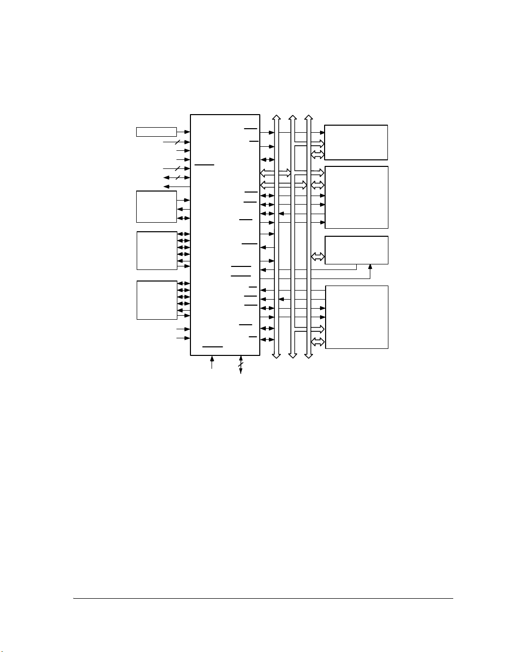
Figure 1-1 shows a detailed block diagram of the processor, illustrating the
following architectural features:
• Two Processing Elements (PEx and PEy), each containing a 32-Bit
IEEE floating-point computation units—multiplier, ALU, Shifter,
and data register file
• Program sequencer with related instruction cache, interval timer,
and Data Address Generators (DAG1 and DAG2)
• Dual-ported SRAM
• External port for interfacing to off-chip memory, peripherals,
hosts, and multiprocessor systems
• Input/Output (IO) processor with integrated DMA controller,
serial ports, and link ports for point-to-point multiprocessor
communications
• JTAG Test Access Port for emulation
Figure 1-1 also shows the three on-chip buses of the ADSP-21160: the
Program Memory (PM) bus, Data Memory (DM) bus, and Input/Output
(IO) bus. The PM bus provides access to either instructions or data. During a single cycle, these buses let the processor access two data operands
(one from PM and one from DM), access an instruction (from the cache),
and perform a DMA transfer.
ADSP-21160 SHARC DSP Hardware Reference 1-3

ADSP-21160 DSP Design Advantages
The buses connect to the ADSP-21160 DSP’s external port, which provides the processor’s interface to external memory, memory-mapped I/O,
a host processor, and additional multiprocessing ADSP-21160 DSPs. The
external port performs bus arbitration and supplies control signals to
shared, global memory and I/O devices.
CORE PROCESSOR
DAG2
DAG1
8x4x32
8x4x32
BUS
CONNECT
(PX)
DATA
REGISTER
FILE
(PEx)
16 x 40-BIT
MULT
TIMER
PROGRAM
SEQUENCER
PM ADDRESS BUS
DM ADDRESS BUS
PM DATA BUS
DM DATA BUS
BARREL
SHIFTER
ALU
INSTRUCTION
CACHE
32 x 48-BIT
32
32
48/64
32/40/64
BARREL
SHIFTER
ALU
DUAL-PORTED SRAM
TWO INDEPENDENT
DUAL-PORTED BLOCKS
PROCESSOR PORT I/ O PORT
ADDR DATA ADDR
ADDR DATA
DATA
REGISTER
FILE
(PEy)
16 x 40-BIT
MULT
DATA
DATA
IOD
64
REGISTERS
MEMORY MAPPED)
(
CONTROL,
STATUS, &
DATA BUFFERS
IOP
ADDR
IOA
32
0
K
C
O
L
B
1
K
C
O
L
B
JTAG
TEST &
EMULATION
EXTERNAL
PORT
ADDR BUS
MUX
MULTIPROCESSOR
INTERFACE
DATA BUS
MUX
HOST PORT
DMA
CONTROLLER
SERIAL PORTS
(2)
LINK PORTS
(6)
6
32
64
4
6
6
60
I/O PROCESSOR
Figure 1-1. ADSP-21160 SHARC DSP Block Diagram
Figure 1-2 illustrates a typical single-processor system. The ADSP-21160
DSP includes extensive support for multiprocessor systems as well. For
more information, see “Multiprocessor (DSPs) Interface” on page 7-96.
Further, the ADSP-21160 DSP addresses the five central requirements for
DSPs:
• Fast, flexible arithmetic computation units
• Unconstrained data flow to and from the computation units
1-4 ADSP-21160 SHARC DSP Hardware Reference
Introduction
ADSP-2116X
CLOCK
LINK
DEVICES
(6 MAX)
(OPTIONAL)
SERIAL
SERIAL
DEVICE
DEVICE
(OPTIONAL)
(OPTIONAL)
SERIAL
SERIAL
DEVICE
DEVICE
(OPTIONAL)
(OPTIONAL)
4
3
4
CLKIN
CLK_CFG3-0
EBOOT
LBOOT
IRQ2-0
FLAG3-0
TIMEXP
LXCLK
LXACK
LXDAT7-0
TCLK0
RCLK0
TFS0
RSF0
DT0
DR0
TCLK1
RCLK1
TFS1
RSF1
DT1
DR1
RPBA
ID2-0
RESET
BMS
CIF
BRST
ADDR31-0
DATA63-0
RDX
WRX
ACK
MS3-0
PAGE
SBTS
CLKOUT
DMAR1-2
DMAG1-2
CS
HBR
HBG
REDY
BR1-6
PA
JTAG
6
L
O
R
T
N
O
C
Figure 1-2. ADSP-21160 Processor System
CS
ADDR
DATA
ADDR
DATA
OE
WE
ACK
CS
S
S
A
E
T
R
A
D
D
D
A
DATA
ADDR
DATA
BOOT
EPROM
(OPTIONAL)
MEMORY
AND
PERIPHERALS
(OPTIONAL)
DMA DEVICE
(OPTIONAL)
HOST
PROCESSOR
INTERFACE
(OPTIONAL)
• Extended precision and dynamic range in the computation units
• Dual address generators with circular buffering support
• Efficient program sequencing
Fast, Flexible Arithmetic. The ADSP-21000 Family processors execute all
instructions in a single cycle. They provide both fast cycle times and a
complete set of arithmetic operations. The DSP is IEEE floating-point
compatible and allows either interrupt on arithmetic exception or latched
status exception handling.
ADSP-21160 SHARC DSP Hardware Reference 1-5

ADSP-21160 DSP Architecture Overview
Unconstrained Data Flow. The ADSP-21160 DSP has a Super Harvard
Architecture combined with a 10-port data register file. In every cycle, the
DSP can write or read two operands to or from the register file, supply
two operands to the ALU, supply two operands to the multiplier, and
receive three results from the ALU and multiplier. The processor’s 48-bit
orthogonal instruction word supports parallel data transfers and arithmetic operations in the same instruction.
40-Bit Extended Precision. The DSP handles 32-bit IEEE floating-point
format, 32-bit integer and fractional formats (twos-complement and
unsigned), and extended-precision 40-bit floating-point format. The processors carry extended precision throughout their computation units,
limiting intermediate data truncation errors.
Dual Address Generators. The DSP has two data address generators
(DAGs) that provide immediate or indirect (pre- and post-modify)
addressing. Modulus, bit-reverse, and broadcast operations are supported
with no constraints on data buffer placement.
Efficient Program Sequencing. In addition to zero-overhead loops, the
DSP supports single-cycle setup and exit for loops. Loops are both
nestable (six levels in hardware) and interruptable. The processors support
both delayed and non-delayed branches.
ADSP-21160 DSP Architecture Overview
The ADSP-21160 DSP forms a complete system-on-a-chip, integrating a
large, high-speed SRAM and I/O peripherals supported by a dedicated
I/O bus. The following sections summarize the features of each functional
block in the ADSP-21160 SHARC architecture, which appears in
Figure 1-1 on page 1-4. With each summary, a cross reference points to
the sections where the features are described in greater detail.
1-6 ADSP-21160 SHARC DSP Hardware Reference

Introduction
Processor Core
The processor core of the ADSP-21160 DSP consists of two processing
elements (each with three computation units and data register file), a program sequencer, two data address generators, a timer, and an instruction
cache. All digital signal processing occurs in the processor core.
Processing Elements
The processor core contains two Processing Elements (PEx and PEy).
Each element contains a data register file and three independent computation units: an ALU, a multiplier with a fixed-point accumulator, and a
shifter. For meeting a wide variety of processing needs, the computation
units process data in three formats: 32-bit fixed-point, 32-bit floating-point and 40-bit floating-point. The floating-point operations are
single-precision IEEE-compatible. The 32-bit floating-point format is the
standard IEEE format, whereas the 40-bit extended-precision format has
eight additional Least Significant Bits (LSBs) of mantissa for greater
accuracy.
The ALU performs a set of arithmetic and logic operations on both
fixed-point and floating-point formats. The multiplier performs floating-point or fixed-point multiplication and fixed-point multiply/add or
multiply/subtract operations. The shifter performs logical and arithmetic
shifts, bit manipulation, field deposit and extraction, and exponent derivation operations on 32-bit operands.
These computation units perform single-cycle operations; there is no computation pipeline. All units are connected in parallel, rather than serially.
The output of any unit may serve as the input of any unit on the next
cycle. In a multifunction computation, the ALU and multiplier perform
independent, simultaneous operations.
Each processing element has a general-purpose data register file that transfers data between the computation units and the data buses and stores
intermediate results. A register file has two sets (primary and alternate) of
ADSP-21160 SHARC DSP Hardware Reference 1-7

ADSP-21160 DSP Architecture Overview
sixteen registers each, for fast context switching. All of the registers are 40
bits wide. The register file, combined with the core processor’s Harvard
architecture, allows unconstrained data flow between computation units
and internal memory.
Primary Processing Element (PEx). PEx processes all computational
instructions whether the DSP is in Single-Instruction, Single-Data (SISD)
or Single-Instruction, Multiple-Data (SIMD) mode. This element corresponds to the computational units and register file in previous
ADSP-21000 DSPs.
Secondary Processing Element (PEy). PEy processes each computational
instruction in lock-step with PEx, but only processes these instructions
when the DSP is in SIMD mode. Because many operations are influenced
by this mode, more information on SIMD is available in multiple
locations:
• For information on PEy operations, see “Processing Elements”
• For information on data addressing in SIMD mode, see “Address-
ing in SISD and SIMD Modes” on page 4-18
• For information on data accesses in SIMD mode, see “SISD,
SIMD, and Broadcast Load Modes” on page 5-44
• For information on multiprocessing in SIMD mode, see “Multi-
processor (DSPs) Interface” on page 7-96.
• For information on SIMD programming, see the ADSP-21160
SHARC DSP Instruction Set Reference.
Program Sequence Control
Internal controls for ADSP-21160 DSP’s program execution come from
four functional blocks: program sequencer, data address generators, timer,
and instruction cache. Two dedicated address generators and a program
sequencer supply addresses for memory accesses. Together the sequencer
1-8 ADSP-21160 SHARC DSP Hardware Reference

Introduction
and data address generators allow computational operations to execute
with maximum efficiency since the computation units can be devoted
exclusively to processing data. With its instruction cache, the
ADSP-21160DSP can simultaneously fetch an instruction from the cache
and access two data operands from memory. The data address generators
implement circular data buffers in hardware.
Program Sequencer. The program sequencer supplies instruction
addresses to program memory. It controls loop iterations and evaluates
conditional instructions. With an internal loop counter and loop stack,
the ADSP-21160 DSP executes looped code with zero overhead. No
explicit jump instructions are required to loop or decrement and test the
counter.
The ADSP-21160 DSP achieves its fast execution rate by means of pipelined fetch, decode and execute cycles. If external memories are used, they
are allowed more time to complete an access than if there were no decode
cycle.
Data Address Generators. The data address generators (DAGs) provide
memory addresses when data is transferred between memory and registers.
Dual data address generators enable the processor to output simultaneous
addresses for two operand reads or writes. DAG1 supplies 32-bit addresses
to data memory. DAG2 supplies 32-bit addresses to program memory for
program memory data accesses.
Each DAG keeps track of up to eight address pointers, eight modifiers and
eight length values. A pointer used for indirect addressing can be modified
by a value in a specified register, either before (pre-modify) or after
(post-modify) the access. A length value may be associated with each
pointer to perform automatic modulo addressing for circular data buffers;
the circular buffers can be located at arbitrary boundaries in memory.
Each DAG register has an alternate register that can be activated for fast
context switching.
ADSP-21160 SHARC DSP Hardware Reference 1-9

ADSP-21160 DSP Architecture Overview
Circular buffers allow efficient implementation of delay lines and other
data structures required in digital signal processing, and are commonly
used in digital filters and Fourier transforms. The DAGs automatically
handle address pointer wraparound, reducing overhead, increasing performance, and simplifying implementation.
Interrupts. The ADSP-21160 DSP has four external hardware interrupts:
three general-purpose interrupts,
IRQ2-0, and a special interrupt for reset.
The processor also has internally generated interrupts for the timer, DMA
controller operations, circular buffer overflow, stack overflows, arithmetic
exceptions, multiprocessor vector interrupts, and user-defined software
interrupts.
For the general-purpose external interrupts and the internal timer interrupt, the ADSP-21160 DSP automatically stacks the arithmetic status and
mode (MODE1) registers in parallel with the interrupt servicing, allowing fifteen nesting levels of very fast service for these interrupts.
Context Switch. Many of the processor’s registers have alternate registers
that can be activated during interrupt servicing for a fast context switch.
The data registers in the register file, the DAG registers, and the multiplier
result register all have alternates. The Primary Registers are active at reset,
while the Alternate (or Secondary) Registers are activated by control bits
in a mode control register.
Timer. The programmable interval timer provides periodic interrupt generation. When enabled, the timer decrements a 32-bit count register every
cycle. When this count register reaches zero, the ADSP-21160 DSP generates an interrupt and asserts its timer expired output. The count register is
automatically reloaded from a 32-bit period register and the count
resumes immediately.
Instruction Cache. The program sequencer includes a 32-word instruction cache that enables three-bus operation for fetching an instruction and
two data values. The cache is selective—only instructions whose fetches
1-10 ADSP-21160 SHARC DSP Hardware Reference

Introduction
conflict with program memory data accesses are cached. This caching
allows full-speed execution of core, looped operations such as digital filter
multiply-accumulates and FFT butterfly processing.
Processor Internal Buses
The processor core has six buses: PM address, PM data, DM address, DM
data, IO address, and IO data. Due to processor’s Harvard Architecture,
data memory stores data operands, while program memory can store both
instructions and data. This architecture allows dual data fetches, when the
instruction is supplied by the cache.
Bus Capacities. The PM address bus and DM address bus transfer the
addresses for instructions and data. The PM data bus and DM data bus
transfer the data or instructions from each type of memory. The PM
address bus is 32 bits wide allowing access of up to 4 Gwords of mixed
instructions and data. The PM data bus is 64 bits wide to accommodate
the 48-bit instructions and 64-bit data.
The DM address bus is 32 bits wide allowing direct access of up to 4G
words of data. The DM data bus is 64 bits wide. The DM data bus provides a path for the contents of any register in the processor to be
transferred to any other register or to any data memory location in a single
cycle. The data memory address comes from one of two sources: an absolute value specified in the instruction code (direct addressing) or the
output of a data address generator (indirect addressing).
The IO address and IO data buses let the IO processor access internal
memory for DMA without delaying the processor core. The IO address
bus is 32 bits wide, and the IO data bus is 64 bits wide.
Data Transfers. Nearly every register in the processor core is classified as a
Universal Register (UREG). Instructions allow transferring data between
any two universal registers or between a universal register and memory.
This support includes transfers between control registers, status registers,
and data registers in the register file. The PM bus connect (
PX) registers
ADSP-21160 SHARC DSP Hardware Reference 1-11

ADSP-21160 DSP Architecture Overview
permit data to be passed between the 64-bit PM data bus and the 64-bit
DM data bus or between the 40-bit register file and the PM data bus.
These registers contain hardware to handle the data width difference. For
more information, see “Processing Element Registers” on page A-16.
Processor Peripherals
The term processor peripherals refers to everything outside the processor
core. The ADSP-21160 DSP’s peripherals include internal memory, external port, I/O processor, JTAG port, and any external devices that connect
to the DSP.
Dual-Ported Internal Memory (SRAM)
The ADSP-21160 DSP contains 4 megabits of on-chip SRAM, organized
as two blocks of 2 Mbits each, which can be configured for different combinations of code and data storage. Each memory block is dual-ported for
single-cycle, independent accesses by the core processor and I/O processor
or DMA controller. The dual-ported memory and separate on-chip buses
allow two data transfers from the core and one from I/O, all in a single
cycle.
All of the memory can be accessed as 16-, 32-, 48-, or 64-bit words. On
the ADSP-21160 DSP, the memory can be configured as a maximum of
128K words of 32-bit data, 256K words of 16-bit data, 80K words of
48-bit instructions (and 40-bit data), or combinations of different word
sizes up to 4 megabits.
The DSP supports a 16-bit floating-point storage format, which effectively doubles the amount of data that may be stored on chip. Conversion
between the 32-bit floating-point and 16-bit floating-point formats completes in a single instruction.
While each memory block can store combinations of code and data,
accesses are most efficient when one block stores data, using the DM bus
for transfers, and the other block stores instructions and data, using the
1-12 ADSP-21160 SHARC DSP Hardware Reference

Introduction
PM bus for transfers. Using the DM bus and PM bus in this way, with one
dedicated to each memory block, assures single-cycle execution with two
data transfers. In this case, the instruction must be available in the cache.
The DSP also maintains single-cycle execution when one of the data operands is transferred to or from off-chip, using the DSP’s external port.
External Port
The ADSP-21160 DSP’s external port provides the processor’s interface
to off-chip memory and peripherals. The 4-gigaword off-chip address
space is included in the ADSP-21160 DSP’s unified address space. The
separate on-chip buses—for PM address, PM data, DM address, DM data,
IO address, and IO data—multiplex at the external port to create an external system bus with a single 32-bit address bus and a single 64-bit data
bus. External SRAM can be 16, 32, 48, or 64 bits wide; the DSP’s on-chip
DMA controller automatically packs external data into the appropriate
word width during transfers.
On-chip decoding of high-order address lines generates memory bank
select signals for addressing external memory devices. Separate control
lines support simplified addressing of page-mode DRAM. The
ADSP-21160 DSP provides programmable memory waitstates and external memory acknowledge controls for interfacing to DRAM and
peripherals with variable access, hold, and disable time requirements.
Host Processor Interface. The ADSP-21160 DSP’s host interface allows
easy connection to standard microprocessor buses, both 16-bit and 32-bit,
with little additional hardware required. The interface supports asynchronous and synchronous transfers at speeds up to the half the internal clock
rate of the ADSP-21160 DSP. The host interface operates through the
DSP’s external port and maps into the unified address space. Four channels of DMA are available for the host interface; code and data transfers
occur with low software overhead. The host can directly read and write the
ADSP-21160 SHARC DSP Hardware Reference 1-13

ADSP-21160 DSP Architecture Overview
internal memory of the ADSP-21160 DSP and can access the DMA channel setup and mailbox registers. Vector interrupt support provides for
efficient execution of host commands.
Multiprocessor System Interface. The ADSP-21160 DSP offers powerful
features tailored to multiprocessing DSP systems. The unified address
space allows direct interprocessor accesses of each ADSP-21160 DSP’s
internal memory. Distributed bus arbitration logic on the DSP allows
simple, glueless connection of systems containing up to six ADSP-21160
DSPs and a host processor. Master processor changeover incurs only one
cycle of overhead. Bus arbitration handles either fixed or rotating priority.
Processor bus lock allows indivisible read-modify-write sequences for
semaphores. A vector interrupt capability is provided for interprocessor
commands. Broadcast writes allow simultaneous transmission of data to
all ADSP-21160 DSPs and can be used to implement reflective
semaphores.
I/O Processor
The ADSP-21160 DSP’s Input/Output Processor (IOP) includes two
serial ports, six link ports, and a DMA controller. One of the I/O processes that the IO processor automates is booting. The DSP can boot from
the external port (with data from an 8-bit EPROM or a host processor) or
a link port. Alternatively, a no-boot mode lets the DSP start by executing
instructions from external memory without booting.
Serial Ports. The ADSP-21160 DSP features two synchronous serial ports
that provide an inexpensive interface to a wide variety of digital and
mixed-signal peripheral devices. The serial ports can operate at up to half
the processor core clock rate. Independent transmit and receive functions
provide greater flexibility for serial communications. Serial port data can
automatically transfer to and from on-chip memory using DMA. Each of
the serial ports offers a TDM multichannel mode and supports m-law or
A-law companding.
1-14 ADSP-21160 SHARC DSP Hardware Reference

Introduction
The serial ports can operate with little-endian or big-endian transmission
formats, with word lengths selectable from 3 to 32 bits. They offer selectable synchronization and transmit modes. Serial port clocks and frame
syncs can be internally or externally generated.
Link Ports. The ADSP-21160 DSP features six 8-bit link ports that provide additional I/O capabilities. Link port I/O is especially useful for
point-to-point interprocessor communication in multiprocessing systems.
The link ports can operate independently and simultaneously. The data
packs into 32-bit or 48-bit words, which the processor core can directly
read or the IO processor can DMA-transfer to on-chip memory.
Clock/acknowledge handshaking controls link port transfers. Transfers are
programmable as either transmit or receive.
DMA Controller. The ADSP-21160 DSP’s on-chip DMA controller
allows zero-overhead data transfers without processor intervention. The
DMA controller operates independently and invisibly to the processor
core to enable DMA operations to occur while the core is simultaneously
executing its program. Both code and data can be downloaded to the
ADSP-21160 DSP using DMA transfers.
DMA transfers can occur between the ADSP-21160 DSP’s internal memory and external memory, external peripherals, or a host processor. DMA
transfers can also occur between the ADSP-21160 DSP’s internal memory
and its serial ports or link ports. DMA transfers between external memory
and external peripheral devices are another option. External bus packing
to 16-, 32-, 48-, or 64-bit words is automatically performed during DMA
transfers.
Fourteen channels of DMA are available on the ADSP-21160 DSP—six
over the link ports, four over the serial ports, and four over the processor’s
external port. The external port DMA channels serve for host processor,
other ADSP-21160 DSPs, memory, or I/O transfers.
ADSP-21160 SHARC DSP Hardware Reference 1-15

Development Tools
JTAG Port
The JTAG port on the ADSP-21160 DSP supports the IEEE standard
1149.1 Joint Test Action Group (JTAG) standard for system test. This
standard defines a method for serially scanning the I/O status of each
component in a system. Emulators use the JTAG port to monitor and
control the DSP during emulation. Emulators using this port provide
full-speed emulation with access to inspect and modify memory, registers,
and processor stacks. JTAG-based emulation is non-intrusive and does not
effect target system loading or timing.
Development Tools
The ADSP-21160 DSP is supported by VisualDSP++™, an easy-to-use
project management environment, comprised of an Integrated Development Environment (IDDE) and Debugger. VisualDSP++ lets you manage
projects from start to finish from within a single, integrated interface.
Because the project development and debug environments are integrated,
you can move easily between editing, building, and debugging activities.
Flexible Project Management. The VisualDSP++ IDDE provides flexible
project management for the development of DSP applications. The IDDE
includes access to all the activities necessary to create and debug DSP
projects. You can create or modify source files or view listing or map files
with the IDDE Editor. This powerful Editor is part of the IDDE and
includes multiple language syntax highlighting, OLE drag and drop,
bookmarks, and standard editing operations such as undo/redo,
find/replace, copy/paste/cut, and go to.
Also, the VisualDSP++ IDDE includes access to the SHARC DSP C
Compiler, C Runtime Library, Assembler, Linker, Loader, Simulator, and
Splitter. You specify options for these SHARC Tools through Property
Page dialog boxes. Property Page dialog boxes are easy to use, and make
configuring, changing, and managing your projects simple. These options
1-16 ADSP-21160 SHARC DSP Hardware Reference

Introduction
control how the tools process inputs and generate outputs, and have a
one-to-one correspondence to the tools’ command line switches. You can
define these options once, or modify them to meet changing development
needs. You can also access the SHARC Tools from the operating system
command line.
Greatly Reduced Debugging Time. The Debugger has an easy-to-use,
common interface for all processor simulators and emulators available
through Analog Devices and third parties or custom developments. The
Debugger has many features that greatly reduce debugging time. You can
view C source interspersed with the resulting Assembly code; profile the
execution of an instruction range in a program; set simulated watch points
on hardware and software registers and on program and data memory.
You can trace instruction execution and memory accesses. These features
enable you to correct coding errors, identify bottlenecks, and examine
DSP performance. You can use the custom register option to select any
combination of registers to view in a single window. The Debugger can
also generate inputs, outputs, and interrupts so you can simulate real
world application conditions.
SHARC Software Development Tools. SHARC Software Development
Tools, which support the SHARC DSPs, allow you to develop applications that take full advantage of the SHARC architecture, including
multiprocessing, shared memory, and memory overlays. SHARC Software
Development Tools include C Compiler, C Runtime Library, DSP and
Math Libraries, Assembler, Linker, Loader, Simulator, and Splitter.
C Compiler and Assembler. The C Compiler generates efficient code that
is optimized for both code density and execution time. The C Compiler
allows you to include Assembly language statements inline. Because of
this, you can program in C and still use Assembly for time-critical loops.
You can also use pretested Math, DSP, and C Runtime Library routines to
help shorten your time to market. The SHARC Assembly language is
ADSP-21160 SHARC DSP Hardware Reference 1-17

Development Tools
based on an algebraic syntax that is easy to learn, program, and debug.
The add instruction, for example, is written in the same manner as the
actual equation.
Linker and Loader. The Linker provides flexible system definition
through Linker Description Files (
.LDF). In a single LDF, you can define
different types of executables for a single or multiprocessor system. The
Linker resolves symbols over multiple executables, maximizes memory use,
and easily shares common code among multiple processors. The Loader
supports creation of host, link port, and PROM boot images. Along with
the Linker, the Loader allows multiprocessor system configuration with
smaller code and faster boot time. The Simulator is a cycle-accurate,
instruction-level simulator, which enables you to simulate your application in real time.
Third-Party Extensible. The VisualDSP++ environment enables
third-party companies to add value using Analog Devices’ published set of
Application Programming Interfaces (API). Third party products—runtime operating systems, emulators, high-level language compilers,
multiprocessor hardware—can interface seamlessly with VisualDSP++
thereby simplifying the tools integration task. VisualDSP++ follows the
COM API format. Two API tools, Target Wizard and API Tester, are also
available for use with the API set. These tools help speed the time-to-market for vendor products. Target Wizard builds the programming shell
based on API features the vendor requires. The API tester exercises the
individual features independently of VisualDSP++. Third parties can use a
subset of these APIs that meets their application needs. The interfaces are
fully supported and backward compatible.
Further details and ordering information are available in the VisualDSP++
Development Tools Data Sheet. This data sheet can be requested from any
Analog Devices sales office or distributor.
1-18 ADSP-21160 SHARC DSP Hardware Reference

Introduction
Differences From Previous SHARC DSPs
This section identifies differences between the ADSP-21160 DSP and previous SHARC DSPs: ADSP-21060, ADSP-21061, and ADSP-21062
processors. The ADSP-21160 DSP preserves much of the ADSP-2106x
architecture, while extending performance and functionality. For background information on SHARC and the ADSP-2106x DSPs, see the
ADSP-2106x SHARC User’s Manual.
Processor Core Enhancements
Computational bandwidth on the ADSP-21160 DSP is significantly
greater that on the ADSP-2106x DSPs. The increase comes from raising
the operational frequency and adding another processing element: ALU,
Shifter, Multiplier, and register file. The new processing element lets the
DSP process multiple data streams in parallel (SIMD mode).
The program sequencer on the ADSP-21160 DSP differs from the
ADSP-2106x DSP family, having several enhancements: new interrupt
vector table definitions, SIMD mode stack and conditional execution
model, and instruction decodes associated with new instructions. Changes
to interrupts include new interrupt vectors for detecting illegal memory
accesses and supporting new unshared DMA channels. Link port interrupt
control has moved to a new register to support the additional DMA channels. Also, new mode stack and mode mask support has been added to
improve context switch time.
Data address generators on the ADSP-21160 DSP differ from the
ADSP-2106x DSPs in that DAG2 (for the PM bus) has the same addressing capability as DAG1 (for the DM bus). The DAG registers are
read/writable in pairs, moving 64-bits/cycle. Additionally, the DAGs support the new memory map and Long Word transfer capability. Circular
buffering on the ADSP-21160 DSP can be quickly disabled on interrupts
ADSP-21160 SHARC DSP Hardware Reference 1-19

Differences From Previous SHARC DSPs
and restored on the return. Data “broadcast”, from one memory location
to both data register files, is determined by appropriate index register
usage.
L
Unlike previous SHARCs, the ADSP-21160 DSP has a global circular buffering enable (CBUFEN) bit. Because at reset this bit defaults
to disabled, programs that use circular buffering and are being
ported from previous SHARCs need to add a line of code to enable
circular buffering. For more information, see “Addressing Circular
Buffers” on page 4-12.
Processor Internal Bus Enhancements
The PM, DM, and IO data buses on the ADSP-21160 DSP are much
wider than on the ADSP-2106x DSPs, increasing to 64 bits. Additional
multiplexing and control logic on the ADSP-21160 DSP enables 16-, 32-,
or 64-bit wide moves between both register files and memory.
The ADSP-21160 DSP also has the capability of broadcasting a single
memory location to each of the register files in parallel. Also, the
ADSP-21160 DSP permits register contents to be exchanged between the
two processing elements’ register files in a single cycle.
Memory Organization Enhancements
The ADSP-21160 memory map differs from the ADSP-2106x DSPs. The
system memory map on the ADSP-21160DSP supports double-word
transfers each cycle, reflects extended internal memory capacity for derivative designs, and works with updated control register for SIMD support.
1-20 ADSP-21160 SHARC DSP Hardware Reference

Introduction
External Port Enhancements
The ADSP-21160 DSP’s external port differs from the ADSP-2106x
DSPs, greatly extending the external interface. The data bus on the
ADSP-21160 DSP is 64 bits wide. The ADSP-21160 DSP has a new synchronous interface that improves local bus switching frequency. Also,
burst support on the ADSP-21160 DSP improves bus usage.
L
Host Interface Enhancements
The ADSP-21160’s host interface differs from the ADSP-2106x DSPs in
that this interface can take advantage of the 64-bit data bus width.
Though the ADSP-21160 DSP supports the ADSP-2106x’s asynchronous
host interface protocols, the ADSP-21160 DSP also provides new synchronous interface protocols for maximum throughput.
The host/local bus deadlock resolution function on the ADSP-21160 DSP
is extended to the DMA controller. The function allows the host (or
bridge) logic to force the local bus to back off and allow the host to complete it’s operation first.
Multiprocessor Interface Enhancements
Unlike previous SHARC DSPs, the ADSP-21160DSP sets the
buffer hang disable (BHD) bit at reset. Because this bit prevents the
processor core from detecting a buffer-related stall condition, programs that use external port, link port, or serial port I/O and are
being ported from previous SHARC DSPs need to add a line of
code to disable BHD. For more information, see the BHD discussion
on page 6-18.
The ADSP-21160’s multiprocessor system interface supports greater
throughput than the ADSP-2106x DSPs. The throughput between
ADSP-21160 DSPs in a multiprocessing application increases due to
shared data bus width increase to 64-bits, new shared bus transfer protocols, shared bus cycle time improvements due to synchronous interface,
ADSP-21160 SHARC DSP Hardware Reference 1-21

Differences From Previous SHARC DSPs
and improvements in Link Port throughput. The external port supports
glueless multiprocessing, with distributed arbitration for up to six
ADSP-21160 DSPs.
IO Architecture Enhancements
The IO processor on the ADSP-21160 DSP provides much greater
throughput than the ADSP-2106x DSPs. The Link Ports and DMA controller differ on the ADSP-21160 DSP.
DMA Controller Enhancements
The ADSP-21160’s DMA controller supports 14 channels (versus 10 on
the ADSP-2106x DSPs), with no channel sharing. New packing modes
support the new 64-bit external/internal busing. To resolve potential
deadlock scenarios, the ADSP-21106’s DMA controller relinquishes the
local bus in a similar fashion to the processor core when host logic asserts
both HBR and SBTS.
Link Port Enhancements
The ADSP-21160’s Link ports provide greater throughput than the
ADSP-2106x DSPs. The link port data bus width on the ADSP-21160
DSP is 8 bits wide (versus 4 bits on the ADSP-2106x DSPs). Link port
clock control on the ADSP-21160 supports a wider frequency range.
Instruction Set Enhancements
ADSP-21160 DSP provides source code compatibility with the previous
SHARC family members, to the application assembly source code level.
All instructions, control registers, and system resources available in t the
ADSP-2106x core programming model are available in ADSP-21160
DSP.
1-22 ADSP-21160 SHARC DSP Hardware Reference

Introduction
New instructions, control registers, or other facilities, required to support
the new feature set of ADSP-21160 processor core are:
• Supersets of the ADSP-2106x programming model
• Reserved facilities in the ADSP-2106x programming model
• Symbol name changes from the ADSP-2106x programming model
These name changes can be managed through re-assembly using the
ADSP-21160 DSP’s development tools to apply the ADSP-21160 symbol
definitions header file and linker description file. While these changes
have no direct impact on existing core applications, system and I/O processor initialization code and control code do require modifications.
This approach simplifies porting of source code written for the
ADSP-2106x DSPs to ADSP-21160 DSP. Code changes will be required
to take full advantage of the new ADSP-21160 DSP features. For more
information, see the ADSP-21160 SHARC DSP Instruction Set Reference.
For Information About Analog Products
Analog Devices is online on the internet at http://www.analog.com. Our
Web pages provide information on the company and products, including
access to technical information and documentation, product overviews,
and product announcements.
You may also obtain additional information about Analog Devices and its
products in any of the following ways.
• Visit our World Wide Web site at
• FAX questions or requests for information to 1(781)461-3010.
• Access the Computer Products Division File Transfer Protocol
(FTP) site at
ftp://ftp.analog.com.
ftp ftp.analog.com or ftp 137.71.23.21 or
ADSP-21160 SHARC DSP Hardware Reference 1-23
www.analog.com

For Technical or Customer Support
For Technical or Customer Support
You can reach our Customer Support group in the following ways.
• E-mail questions to dsp.support@analog.com or
dsp.europe@analog.com (European customer support)
• Contact your local ADI sales office or an authorized ADI
distributor
• Send questions by mail to:
Analog Devices, Inc.
DSP Division
One Technology Way
P.O. Box 9106
Norwood, MA 02062-9106
USA
What’s New in This Manual
This is the third edition of the ADSP-21160 SHARC DSP Hardware Reference. This edition was updated to correct all open document errata.
Related Documents
For more information about Analog Devices DSPs and development
products, see the following documents:
• ADSP-21160 SHARC DSP Microcomputer Data Sheet
• ADSP-21160 SHARC DSP Instruction Set Reference
• Getting Started Guide for VisualDSP++ and ADSP-21xxx DSPs
1-24 ADSP-21160 SHARC DSP Hardware Reference

Introduction
• VisualDSP++ User's Guide for ADSP-21xxx DSPs
• VisualDSP++ C Compiler and Library Manual for ADSP-21xxx
DSPs
• VisualDSP++ Assembler Manual for ADSP-21xxx DSPs
• VisualDSP++ Linker and Utilities Manual for ADSP-21xxx DSPs
All the manuals are included in the software distribution CD-ROM. To
access these manuals, use the Help Topics command in the VisualDSP++
environment’s Help menu and select the Online Manuals book. From this
Help topic, you can open any of the manuals, which are in Adobe Acrobat
PDF format.
Conventions
The following are conventions that apply to all chapters. Note that additional conventions, which apply only to specific chapters, appear
throughout this document.
Table 1-1. Notation Conventions
Example Description
PC, R1, PX Register names appear in UPPERCASE and keyword font
TIMEXP, RESET Pin names appear in UPPERCASE and keyword font; active low signals
appear with an OVERBAR
If, Do/Until Assembler instructions (mnemonics) appear in initial capitals
A note, providing information of special interest or identifying a related
L
DSP topic.
.
ADSP-21160 SHARC DSP Hardware Reference 1-25

Conventions
Table 1-1. Notation Conventions (Cont’d)
Example Description
A caution, providing information on critical design or programming
[
Click Here In the online version of this document, a cross reference acts as a hyper-
issues that influence operation of the DSP.
text link to the item being referenced. Click on blue references (Table,
Figure, or section names) to jump to the location.
1-26 ADSP-21160 SHARC DSP Hardware Reference

2 PROCESSING ELEMENTS
The DSP’s Processing Elements (PEx and PEy) perform numeric processing for DSP algorithms. Each processing element contains a data register
file and three computation units: an arithmetic/logic unit (ALU), a multiplier, and a shifter. Computational instructions for these elements include
both fixed-point and floating-point operations, and each computational
instruction can execute in a single cycle.
Overview
The computational units in a processing element handle different types of
operations. The ALU performs arithmetic and logic operations on
fixed-point and floating-point data. The multiplier does floating-point
and fixed-point multiplication and executes fixed-point multiply/add and
multiply/subtract operations. The shifter completes logical shifts, arithmetic shifts, bit manipulation, field deposit, and field extraction
operations on 32-bit operands. Also, the Shifter can derive exponents.
Data flow paths through the computational units are arranged in parallel,
as shown in Figure 2-1. The output of any computation unit may serve as
the input of any computation unit on the next instruction cycle. Data
moving in and out of the computational units goes through a 10-port register file, consisting of sixteen primary registers and sixteen alternate
registers. Two ports on the register file connect to the PM and DM data
buses, allowing data transfer between the computational units and memory (and anything else) connected to these buses.
ADSP-21160 SHARC DSP Hardware Reference 2-1

Setting Computational Modes
The DSP’s assembly language provides access to the data register files in
both processing elements. The syntax lets programs move data to and
from these registers and specify a computation’s data format at the same
time with naming conventions for the registers. For information on the
data register names, see “Data Register File” on page 2-28 provides a
graphical guide to the other topics in this chapter. First, a description of
the
MODE1 register shows how to set rounding, data format, and other
modes for the processing elements. Next, an examination of each computational unit provides details on operation and a summary of
computational instructions. Outside the computational units, details on
register files and data buses identify how to flow data for computations.
Finally, details on the DSP’s advanced parallelism reveal how to take
advantage of multifunction instructions and SIMD mode.
Setting Computational Modes
The MODE1 register controls the operating mode of the processing elements. Table A-2 on page A-3 lists all the bits in MODE1. The following bits
in MODE1 control computational modes:
• Floating-point data format. Bit 16 (RND32) directs the computational units to round floating-point data to 32 bits (if 1) or round
to 40 bits (if 0)
• Rounding mode. Bit 15 (
TRUNC) directs the computational units to
round results with round-to-zero (if 1) or round-to-nearest (if 0)
• ALU saturation. Bit 13 (
ALUSAT) directs the computational units to
saturate results on positive or negative fixed-point overflows (if 1)
or return unsaturated results (if 0)
2-2 ADSP-21160 SHARC DSP Hardware Reference

Processing Elements
MODE1
XY Z XYXY
MUL TI P LIER
TO PROGRAM SEQUENCER
Figure 2-1. Computations Units
PM DA TA BUS
DM D ATA BUS
REGISTER FILE
(16 × 40 -BI T)
R0
R1
R2
R3
R4
R5
R6
R7
MRF2 MRF 0MRF1
ASTATx STKYx
R8
R9
R10
R11
R12
R13
R14
R15
SHIFTER ALU
• Short word sign extension. Bit 14 (SSE) directs the computational
units to sign extend short-word, 16-bit data (if 1) or zero-fill the
upper 16 bits (if 0)
• Secondary processor element (PEy). Bit 21 (PEYEN) enables com-
putations in PEy—SIMD mode—(if 1) or disables PEy—SISD
mode—(if 0)
ADSP-21160 SHARC DSP Hardware Reference 2-3

Setting Computational Modes
32-bit (Normal Word) Floating-Point Format
In the default mode of the DSP (RND32 bit=1), the multiplier and ALU
support a single-precision floating-point format, which is specified in the
IEEE 754/854 standard. For more information on this standard, see
“Numeric Formats”. This format is IEEE 754/854 compatible for sin-
gle-precision floating-point operations in all respects except that:
• The DSP does not provide inexact flags.
• NAN (“Not-A-Number”) inputs generate an invalid exception and
return a quiet NAN (all 1s).
• Denormal operands flush to zero when input to a computation
unit and do not generate an underflow exception. Any denormal or
underflow result from an arithmetic operation flushes to zero and
generates an underflow exception.
• The DSP supports round to nearest and round toward zero modes,
but does not support round to +Infinity and round to -Infinity.
IEEE single-precision floating-point data uses a 23-bit mantissa with an
8-bit exponent plus sign bit. In this case, the computation unit sets the
eight LSBs of floating-point inputs to zeros before performing the operation. The mantissa of a result rounds to 23 bits (not including the hidden
bit), and the 8 LSBs of the 40-bit result clear to zeros to form a 32-bit
number, which is equivalent to the IEEE standard result.
In fixed-point to floating-point conversion, the rounding boundary is
always 40 bits even if the
RND32 bit is set.
40-bit Floating-Point Format
When in extended precision mode (RND32 bit=0), the DSP supports a
40-bit extended precision floating-point mode, which has eight additional
LSBs of the mantissa and is compliant with the 754/854 standards; how-
2-4 ADSP-21160 SHARC DSP Hardware Reference

Processing Elements
ever, results in this format are more precise than the IEEE single-precision
standard specifies. Extended-precision floating-point data uses a 31-bit
mantissa with a 8-bit exponent plus sign bit.
16-bit (Short Word) Floating-Point Format
The DSP supports a 16-bit floating-point storage format and provides
instructions that convert the data for 40-bit computations. The 16-bit
floating-point format uses an 11-bit mantissa with a 4-bit exponent plus
sign bit. The 16-bit data goes into bits 23 through 8 of a data register.
Two shifter instructions, Fpack and Funpack, perform the packing and
unpacking conversions between 32-bit floating-point words and 16-bit
floating-point words. The Fpack instruction converts a 32-bit IEEE floating-point number in a data register into a 16-bit floating-point number.
Funpack converts a 16-bit floating-point number in a data register into a
32-bit IEEE floating-point number. Each instruction executes in a single
cycle.
When 16-bit data is written to bits 23 through 8 of a data register, the
DSP automatically extends the data into a 32-bit integer (bits 39 through
8). If the SSE bit in MODE1 is set (1), the DSP sign extends the upper 16
bits. If the SSE bit is cleared (0), the DSP zeros the upper 16 bits.
The 16-bit floating-point format supports gradual underflow. This
method sacrifices precision for dynamic range. When packing a number
that would have underflowed, the exponent clears to zero and the mantissa
(including “hidden” 1) right-shifts the appropriate amount. The packed
result is a denormal, which can be unpacked into a normal IEEE floating-point number.
32-Bit Fixed-Point Format
The DSP always represents fixed-point numbers in 32 bits, occupying the
32 MSBs in 40-bit data registers. Fixed-point data may be fractional or
integer numbers and unsigned or twos-complement. Each computational
ADSP-21160 SHARC DSP Hardware Reference 2-5

Setting Computational Modes
unit has its own limitations on how these formats may be mixed for a
given operation. All computational units read the upper 32 bits of data
(inputs, operands) from the 40-bit registers (ignoring the 8 LSBs) and
write results to the upper 32 bits (zeroing the 8 LSBs).
Rounding Mode
The TRUNC bit in the MODE1 register determines the rounding mode for all
ALU operations, all floating-point multiplies, and fixed-point multiplies
of fractional data. The DSP supports two modes of rounding:
round-toward-zero and round-toward-nearest. The rounding modes comply with the IEEE 754 standard and have the following definitions:
• Round-Toward-Zero (
TRUNC bit=1). If the result before rounding
is not exactly representable in the destination format, the rounded
result is the number that is nearer to zero. This is equivalent to
truncation.
• Round-Toward-Nearest (TRUNC bit=0). If the result before rounding is not exactly representable in the destination format, the
rounded result is the number that is nearer to the result before
rounding. If the result before rounding is exactly halfway between
two numbers in the destination format (differing by an LSB), the
rounded result is the number that has an LSB equal to zero.
Statistically, rounding up occurs as often as rounding down, so there is no
large sample bias. Because the maximum floating-point value is one LSB
less than the value that represents Infinity, a result that is halfway between
the maximum floating-point value and Infinity rounds to Infinity in this
mode.
Though these rounding modes comply with standards set for floating-point data, they also apply for fixed-point multiplier operations on
fractional data. The same two rounding modes are supported, but only the
round-to-nearest operation is actually performed by the multiplier. Using
2-6 ADSP-21160 SHARC DSP Hardware Reference

Processing Elements
its local result register for fixed-point operations, the multiplier
rounds-to-zero by reading only the upper bits of the result and discarding
the lower bits.
Using Computational Status
The multiplier and ALU each provide exception information when executing floating-point operations. Each unit updates overflow, underflow,
and invalid operation flags in the processing element’s arithmetic status
(ASTATx and ASTATy) register and sticky status (STKYx and STKYy) register.
An underflow, overflow, or invalid operation from any unit also generates
a maskable interrupt. There are three ways to use floating-point exceptions from computations in program sequencing:
• Interrupts. Enable interrupts and use an interrupt service routine
to handle the exception condition immediately. This method is
appropriate if it is important to correct all exceptions as they occur.
• ASTATx and ASTATy registers. Use conditional instructions to test
the exception flags in the ASTATx or ASTATy register after the
instruction executes. This method permits monitoring each
instruction’s outcome.
• STKYx and STKYy registers. Use the Bit Tst instruction to examine
exception flags in the
any flags are set, some of the results are incorrect. This method is
useful when exception handling is not critical.
More information on
describe the computational units. For summaries relating instructions and
status bits, see Table 2-1 on page 2-11, Table 2-2 on page 2-12, Table 2-4
on page 2-19,Table 2-6 on page 2-21,and Table 2-7 on page 2-27.
ADSP-21160 SHARC DSP Hardware Reference 2-7
ASTAT and STKY status appears in the sections that
STKY register after a series of operations. If

Arithmetic Logic Unit (ALU)
Arithmetic Logic Unit (ALU)
The ALU performs arithmetic operations on fixed-point or floating-point
data and logical operations on fixed-point data. ALU fixed-point instructions operate on 32-bit fixed-point operands and output 32-bit
fixed-point results. ALU floating-point instructions operate on 32-bit or
40-bit floating-point operands and output 32-bit or 40-bit floating-point
results. ALU instructions include:
• Floating-point addition, subtraction, add/subtract, average
• Fixed-point addition, subtraction, add/subtract, average
• Floating-point manipulation: binary log, scale, mantissa
• Fixed-point add with carry, subtract with borrow, increment,
decrement
• Logical And, Or, Xor, Not
• Functions: Abs, pass, min, max, clip, compare
• Format conversion
• Reciprocal and reciprocal square root primitives
ALU Operation
ALU instructions take one or two inputs: X input and Y input. These
inputs (also known as operands) can be any data registers in the register
file. Most ALU operations return one result; in add/subtract operations,
the ALU operation returns two results, and in compare operations, the
ALU operation returns no result (only flags are updated). ALU results can
be returned to any location in the register file.
2-8 ADSP-21160 SHARC DSP Hardware Reference

Processing Elements
The DSP transfers input operands from the register file during the first
half of the cycle and transfers results to the register file during the second
half of the cycle. With this arrangement, the ALU can read and write the
same register file location in a single cycle. If the ALU operation is
fixed-point, the inputs are treated as 32-bit fixed-point operands. The
ALU transfers the upper 32 bits from the source location in the register
file. For fixed-point operations, the result(s) are always 32-bit fixed-point
values. Some floating-point operations (Logb, Mant and Fix) can also
yield fixed-point results.
The DSP transfers fixed-point results to the upper 32 bits of the data register and clears the lower eight bits of the register. The format of
fixed-point operands and results depends on the operation. In most arithmetic operations, there is no need to distinguish between integer and
fractional formats. Fixed-point inputs to operations such as scaling a floating-point value are treated as integers. For purposes of determining status
such as overflow, fixed-point arithmetic operands and results are treated as
twos-complement numbers.
ALU Saturation
When the ALUSAT bit is set (1) in the MODE1 register, the ALU is in saturation mode. In this mode, all positive fixed-point overflows return the
maximum positive fixed-point number (0x7FFF FFFF), and all negative
overflows return the maximum negative number (
When the ALUSAT bit is cleared (0) in the MODE1 register, fixed-point results
that overflow are not saturated; the upper 32 bits of the result are returned
unaltered.
The ALU overflow flag reflects the ALU result before saturation.
ADSP-21160 SHARC DSP Hardware Reference 2-9
0x8000 0000).

Arithmetic Logic Unit (ALU)
ALU Status Flags
ALU operations update seven status flags in the processing element’s
Arithmetic Status (ASTATx and ASTATy) register. Table A-4 on page A-9
lists all the bits in these registers. The following bits in ASTATx or ASTATy
flag ALU status (a 1 indicates the condition) for the most recent ALU
operation:
• ALU result zero or floating-point underflow. Bit 0 (AZ)
• ALU overflow. Bit 1 (AV)
• ALU result negative. Bit 2 (AN)
• ALU fixed-point carry. Bit 3 (AC)
• ALU X input sign for Abs, Mant operations. Bit 4 (AS)
• ALU floating-point invalid operation. Bit 5 (AI)
• Last ALU operation was a floating-point operation. Bit 10 (AF)
• Compare Accumulation register results of last 8 compare opera-
tions. Bits 31-24 (CACC)
ALU operations also update four “sticky” status flags in the processing element’s Sticky status (STKYx and STKYy) register. Table A-5 on page A-14
lists all the bits in these registers. The following bits in STKYx or STKYy flag
ALU status (a 1 indicates the condition). Once set, a sticky flag remains
high until explicitly cleared:
• ALU floating-point underflow. Bit 0 (AUS)
• ALU floating-point overflow. Bit 1 (
AVS)
• ALU fixed-point overflow. Bit 2 (AOS)
• ALU floating-point invalid operation. Bit 5 (
AIS)
2-10 ADSP-21160 SHARC DSP Hardware Reference

Processing Elements
Flag update occurs at the end of the cycle in which the status is generated
and is available on the next cycle. If a program writes the arithmetic status
register or sticky status register explicitly in the same cycle that the ALU is
performing an operation, the explicit write to the status register supersedes
any flag update from the ALU operation.
ALU Instruction Summary
Table 2-1 and Table 2-2 list the ALU instructions and how they relate to
ASTATx,y and STKYx,y flags. For more information on assembly language
syntax, see the ADSP-21160 SHARC DSP Instruction Set Reference. In
these tables, note the meaning of the following symbols:
• Rn, Rx, Ry indicate a register file location; treated as fixed-point
• Fn, Fx, Fy indicate a register file location; treated as floating-point
• * indicates that the flag may be set or cleared, depending on results
of instruction
• ** indicates that the flag may be set (but not cleared), depending
on results of instruction
• – indicates no effect
Table 2-1. Fixed-Point ALU Instruction Summary
Instruction ASTATx,y Status Flags STKYx,y Status Flags
Fixed-point: AZAV ANACAS AI AF C
Rn = Rx + Ry ****000–––**–
Rn = Rx – Ry ****000–––**–
Rn = Rx + Ry + CI ****000–––**–
Rn = Rx – Ry + CI – 1 ****000–––**–
A
C
C
AUSAVSA
AI
O
S
S
ADSP-21160 SHARC DSP Hardware Reference 2-11

Arithmetic Logic Unit (ALU)
Table 2-1. Fixed-Point ALU Instruction Summary (Cont’d)
Instruction ASTATx,y Status Flags STKYx,y Status Flags
Fixed-point: AZAV ANACAS AI AF C
Rn = (Rx + Ry)/2 *0** 000–––––
COMP(Rx, Ry) *0*0000* ––––
COMPU(Rx,Ry) * 0 * 0 0 0 0 * -- -- -- --
Rn = Rx + CI ****000–––**–
Rn = Rx + CI – 1 ****000–––**–
Rn = Rx + 1 ****000–––**–
Rn = Rx – 1 ****000–––**–
Rn = –Rx ****000–––**–
Rn = ABS Rx ** 00* 00–––**–
Rn = PASS Rx *0*0000–––––
Rn = Rx AND Ry *0*0000–––––
Rn = Rx OR Ry *0*0000–––––
Rn = Rx XOR Ry *0* 0000–––––
Rn = NOT Rx *0*0000–––––
Rn = MIN(Rx, Ry) * 0* 0000–––––
Rn = MAX(Rx, Ry) *0*0000–––––
Rn = CLIP Rx BY Ry * 0*0000–––––
AUSAVSA
A
C
C
AI
O
S
S
Table 2-2. Floating-Point ALU Instruction Summary
Instruction ASTATx,y Status Flags STKYx,y Status Flags
Floating–point: AZ AV AN AC AS AI AF CACCAUSAVSAOSAIS
Fn = Fx + Fy *** 00*1–****–**
Fn = Fx – Fy *** 00*1–****–**
Fn = ABS (Fx + Fy) * * 0 0 0 * 1 – ** ** – **
2-12 ADSP-21160 SHARC DSP Hardware Reference

Processing Elements
Table 2-2. Floating-Point ALU Instruction Summary (Cont’d)
Instruction ASTATx,y Status Flags STKYx,y Status Flags
Floating–point: AZ AV AN AC AS AI AF CACCAUSAVSAOSAIS
Fn = ABS (Fx – Fy) * * 0 0 0 * 1 – ** ** – **
Fn = (Fx + Fy)/2 *0*00* 1–**––**
COMP(Fx, Fy) * 0*00* 1*–––**
Fn = –Fx *** 00*1––**–**
Fn = ABS Fx ** 00** 1––**–**
Fn = PASS Fx *0*00* 1––––**
Fn = RND Fx ** *00* 1––**–**
Fn = SCALB Fx BY Ry*** 00*1–****–**
Rn = MANT Fx * *00* *1––**–**
Rn = LOGB Fx *** 00*1––**–**
Rn = FIX Fx BY Ry *** 00*1–****–**
Rn = FIX Fx *** 00*1–****–**
Fn = FLOAT Rx BY Ry*** 0001–****––
Fn = FLOAT Rx * 0*0001–––––
Fn = RECIPS Fx * * *00* 1–****–**
Fn = RSQRTS Fx * ** 00*1––**–**
Fn = Fx COPYSIGN Fy*0*00* 1––––**
Fn = MIN(Fx, Fy) *0* 00*1––––**
Fn = MAX(Fx, Fy) *0*00* 1––––**
Fn = CLIP Fx BY Fy *0* 00* 1––––**
Multiply—Accumulator (Multiplier)
The multiplier performs fixed-point or floating-point multiplication and
fixed-point multiply/accumulate operations. Fixed-point multiply/accumulates are available with either cumulative addition or cumulative
ADSP-21160 SHARC DSP Hardware Reference 2-13

Multiply—Accumulator (Multiplier)
subtraction. Multiplier floating-point instructions operate on 32-bit or
40-bit floating-point operands and output 32-bit or 40-bit floating-point
results. Multiplier fixed-point instructions operate on 32-bit fixed-point
data and produce 80-bit results. Inputs are treated as fractional or integer,
unsigned or twos-complement. Multiplier instructions include:
• Floating-point multiplication
• Fixed-point multiplication
• Fixed-point multiply/accumulate with addition, rounding optional
• Fixed-point multiply/accumulate with subtraction, rounding
optional
• Rounding result register
• Saturating result register
• Clearing result register
Multiplier Operation
The multiplier takes two inputs: X input and Y input. These inputs (also
known as operands) can be any data registers in the register file. The
multiplier can accumulate fixed-point results in the local Multiplier Result
MRF) registers or write results back to the register file. The results in MRF
(
can also be rounded or saturated in separate operations. Floating-point
multiplies yield floating-point results, which the multiplier always writes
directly to the register file.
The multiplier transfers input operands during the first half of the cycle
and transfers results during the second half of the cycle. With this arrangement, the multiplier can read and write the same register file location in a
single cycle.
2-14 ADSP-21160 SHARC DSP Hardware Reference

Processing Elements
For fixed-point multiplies, the multiplier reads the inputs from the upper
32 bits of the data registers. Fixed-point operands may be either both in
integer format or both in fractional format. The format of the result
matches the format of the inputs. Each fixed-point operand may be either
an unsigned or a twos-complement number. If both inputs are fractional
and signed, the multiplier automatically shifts the result left one bit to
remove the redundant sign bit. The register name(s) within the multiplier
instruction specify input data type(s)—Fx for floating-point and Rx for
fixed-point.
Multiplier (Fixed-Point) Result Register
Fixed-point operations place 80-bit results in the multiplier’s foreground
MRF register or background MRB register, depending on which is active. For
more information on selecting the result register, see “Alternate (Second-
ary) Data Registers” on page 2-31.
The location of a result in the MRF register’s 80-bit field depends on
whether the result is in fractional or integer format, as shown in Table 2-1
on page 2-11. If the result is sent directly to a data register, the 32-bit
result with the same format as the input data is transferred, using bits
63-32 for a fractional result or bits 31-0 for an integer result. The eight
LSBs of the 40-bit register file location are zero-filled.
Fractional results can be rounded-to-nearest before being sent to the register file. If rounding is not specified, discarding bits 31-0 effectively
truncates a fractional result (rounds to zero). For more information on
rounding, see “Rounding Mode” on page 2-6.
MRF register is divided into MRF2, MRF1, and MRF0 registers, which can
The
be individually read from or written to the register file. Each of these registers has the same format. When data is read from MRF2, it is
sign-extended to 32 bits as shown in Figure 2-3. The DSP zero fills the
eight LSBs of the 40-bit register file location when data is read from
MRF1, or MRF0 to the register file. When the DSP writes data into MRF2,
MRF2,
ADSP-21160 SHARC DSP Hardware Reference 2-15

Multiply—Accumulator (Multiplier)
796
0
331
MRF2 MRF0
OVERFLOW UNDERFLOWFRACTIONAL RESULT
OVERFLOW INTEGER RESULTOVERFLOW
MRF1
Figure 2-2. Multiplier Fixed-Point Result Placement
MRF1, or MRF0 from the 32 MSBs of a register file location, the eight LSBs
are ignored. Data written to MRF1 is sign-extended to MRF2, repeating the
MSB of MRF1 in the 16 bits of MRF2. Data written to MRF0 is not
sign-extended.
16 BI T S 1 6 BIT S 16 BI T S
MRF2
ZEROSSIGN EX TEND
8BITS32 B ITS
MRF1
ZEROS
8- BITS32-BITS
MRF0
ZEROS
Figure 2-3. MR Transfer Formats
In addition to multiplication, fixed-point operations include accumulation, rounding and saturation of fixed-point data. There are three
MRF
register operations: Clear, Round, and Saturate.
2-16 ADSP-21160 SHARC DSP Hardware Reference

Processing Elements
The clear operation—
MRF=0—resets the specified MRF register to zero.
Often, it is best to perform this operation at the start of a multiply/accumulate operation to remove results left over from the previous operation.
The rounding operation—MRF=Rnd MRF—applies only to fractional
results, so integer results are not effected. This operation rounds the
80-bit MRF value to nearest at bit 32; for example, the MRF1-MRF0 boundary.
Rounding of a fixed-point result occurs either as part of a multiply or multiply/accumulate operation or as an explicit operation on the MRF register.
The rounded result in MRF1 can be sent either to the register file or back to
the same MRF register. To round a fractional result to zero (truncation)
instead of to nearest, a program would transfer the unrounded result from
MRF1, discarding the lower 32 bits in MRF0.
The saturate operation—MRF=Sat MRF—sets MRF to a maximum value if the
MRF value has overflowed. Overflow occurs when the MRF value is greater
than the maximum value for the data format—unsigned or twos-complement and integer or fractional—as specified in the saturate instruction.
The six possible maximum values appear in Table 2-3. The result from
MRF saturation can be sent either to the register file or back to the same MRF
register.
Table 2-3. Fixed-Point Format Maximum Values (for Saturation)
Maximum Number (Hexadecimal)
MRF2 MRF1 MRF0
2’s complement fractional (positive) 0000 7FFF FFFF FFFF FFFF
2’s complement fractional (negative) FFFF 8000 0000 0000 0000
2’s complement integer (positive) 0000 0000 0000 7FFF FFFF
2’s complement integer (negative) FFFF FFFF FFFF 8000 0000
Unsigned fractional number 0000 FFFF FFFF FFFF FFFF
Unsigned integer number 0000 0000 0000 FFFF FFFF
ADSP-21160 SHARC DSP Hardware Reference 2-17

Multiply—Accumulator (Multiplier)
Multiplier Status Flags
Multiplier operations update four status flags in the processing element’s
arithmetic status register (ASTATx and ASTATy). Table A-4 on page A-9 lists
all the bits in these registers. The following bits in ASTATx or ASTATy flag
multiplier status (a 1 indicates the condition) for the most recent multiplier operation:
• Multiplier result negative. Bit 6 (MN)
• Multiplier overflow. Bit 7 (MV)
• Multiplier underflow. Bit 8 (MU)
• Multiplier floating-point invalid operation. Bit 9 (MI)
Multiplier operations also update four “sticky” status flags in the processing element’s Sticky status (STKYx and STKYy) register. Table A-5 on
page A-14 lists all the bits in these registers. The following bits in STKYx or
STKYy flag multiplier status (a 1 indicates the condition). Once set, a sticky
flag remains high until explicitly cleared:
• Multiplier fixed-point overflow. Bit 6 (MOS)
• Multiplier floating-point overflow. Bit 7 (MVS)
• Multiplier underflow. Bit 8 (MUS)
• Multiplier floating-point invalid operation. Bit 9 (MIS)
Flag update occurs at the end of the cycle in which the status is generated
and is available on the next cycle. If a program writes the arithmetic status
register or sticky register explicitly in the same cycle that the multiplier is
performing an operation, the explicit write to
ASTAT or STKY supersedes
any flag update from the multiplier operation.
2-18 ADSP-21160 SHARC DSP Hardware Reference

Processing Elements
Multiplier Instruction Summary
Table 2-4 on page 2-19 and Table 2-6 on page 2-21 list the Multiplier
instructions and how they relate to ASTATx,y and STKYx,y flags. For more
information on assembly language syntax, see the ADSP-21160 SHARC
DSP Instruction Set Reference. In these tables, note the meaning of the following symbols:
• Rn, Rx, Ry indicate any register file location; treated as fixed-point
• Fn, Fx, Fy indicate any register file location; treated as
floating-point
• * indicates the flag may be set or cleared, depending on results of
instruction
• ** indicates the flag may be set (but not cleared), depending on
results of instruction
• – indicates no effect
• The Input Mods column indicates the types of optional modifiers
that you can apply to the instructions inputs. For a list of modifiers, see Table 2-5.
Table 2-4. Fixed-Point Multiplier Instruction Summary
Instruction Input
Fixed-Point:
For Input Mods, see
Table 2-5
Rn = Rx * Ry 1 ***0–**––
MRF = Rx * Ry 1 ***0–**––
MRB = Rx * Ry 1 ***0–**––
Rn = MRF + Rx * Ry 1 ***0–**––
Rn = MRB + Rx * Ry1 ***0–**––
Mods
ASTATx,y Flags STKYx,y Flags
MUMNMVMIM
M
U
O
S
S
M
V
S
M
I
S
ADSP-21160 SHARC DSP Hardware Reference 2-19

Multiply—Accumulator (Multiplier)
Table 2-4. Fixed-Point Multiplier Instruction Summary (Cont’d)
Instruction Input
Fixed-Point:
For Input Mods, see
Table 2-5
MRF = MRF + Rx * Ry1 ***0–**––
MRB = MRB + Rx * Ry1 ***0–**––
Rn = MRF – Rx * Ry 1 ***0–**––
Rn = MRB – Rx * Ry 1 ***0–**––
MRF = MRF – Rx * Ry1 ***0–**––
MRB = MRB – Rx * Ry1 ***0–**––
Rn = SAT MRF 2 ***0–**––
Rn = SAT MRB 2 ***0–**––
MRF = SAT MRF 2 ***0–**––
MRB = SAT MRB 2 ***0–**––
Rn = RND MRF 3 ***0–**––
Rn = RND MRB 3 ***0–**––
MRF = RND MRF 3 ***0–**––
MRB = RND MRB 3 ***0–**––
MRF= 0 – 0000––––
MRB= 0 – 0000––––
MRxF = Rn – 0000––––
MRxB = Rn – 0000––––
Rn = MRxF – 0000––––
Rn = MRxB – 0000––––
Mods
ASTATx,y Flags STKYx,y Flags
MUMNMVMIM
M
U
O
S
S
M
V
S
M
I
S
2-20 ADSP-21160 SHARC DSP Hardware Reference

Processing Elements
Table 2-5. Input Modifiers for Fixed-Point Multiplier Instruction
Input
Mods
from
Table
2-2
1 (SSF), (SSI), (SSFR), (SUF), (SUI), (SUFR), (USF), (USI), (USFR), (UUF),
2 (SF), (SI), (UF), or (UI)
3 (SF) or (UF)
Input Mods—Options For Fixed-point Multiplier Instructions
Note the meaning of the following symbols in this table:
SSigned input
UUnsigned input
IInteger input(s)
FFractional input(s)
FRFractional inputs, Rounded output
Note that (SF) is the default format for 1-input operations, and (SSF) is the
default format for 2-input operations
(UUI), or (UUFR)
Table 2-6. Floating-Point Multiplier Instruction Summary
Instruction ASTATx,y Flags STKYx,y Flags
Floating-Point: MUM
Fn = Fx * Fy * * * * ** – ** **
M
M
M
M
M
N
V
I
U
O
V
S
S
S
M
I
S
Barrel-Shifter (Shifter)
The shifter performs bit-wise operations on 32-bit fixed-point operands.
Shifter operations include:
• Shifts and rotates from off-scale left to off-scale right
• Bit manipulation operations, including bit set, clear, toggle, and
test
ADSP-21160 SHARC DSP Hardware Reference 2-21

Barrel-Shifter (Shifter)
• Bit field manipulation operations, including extract and deposit
• Fixed-point/floating-point conversion operations, including exponent extract, number of leading 1s or 0s
Shifter Operation
The shifter takes from one to three inputs: X-input, Y-input, and Z-input.
The inputs (also known as operands) can be any register in the register
file. Within a shifter instruction, the inputs serve as follows:
• The X-input provides data that is operated on
• The Y-input specifies shift magnitudes, bit field lengths or bit
positions
• The Z-input provides data that is operated on and updated
In the following example, Rx is the X-input, Ry is the Y-input, and Rn is
the Z-input. The shifter returns one output (Rn) to the register file.
Rn = Rn OR LSHIFT Rx BY Ry;
As shown in Figure 2-4, the shifter fetches input operands from the upper
32 bits of a register file location (bits 39-8) or from an immediate value in
the instruction. The shifter transfers operands during the first half of the
cycle and transfers the result to the upper 32 bits of a register (with the
eight LSBs zero-filled) during the second half of the cycle. With this
arrangement, the shifter can read and write the same register file location
in a single cycle.
The X-input and Z-input are always 32-bit fixed-point values. The
Y-input is a 32-bit fixed-point value or an 8-bit field (shf8), positioned in
the register file. These inputs appear in Figure 2-4.
2-22 ADSP-21160 SHARC DSP Hardware Reference

Processing Elements
Some shifter operations produce 8-bit or 6-bit results. As shown in
Figure 2-5, the shifter places these results in either the shf8 field or the
bit6 field and sign-extends the results to 32 bits. The shifter always returns
a 32-bit result.
39 70
32-BIT Y-INPUT OR RESULT
39 15 7 0
SHF8
8-BIT Y-INPUT OR RESULT
Figure 2-4. Register File Fields for Shifter Instructions
The shifter supports bit field deposit and bit field extract instructions for
manipulating groups of bits within an input. The Y-input for bit field
instructions specifies two 6-bit values: bit6 and len6, which are positioned
in the Ry register as shown in Figure 2-5. The shifter interprets bit6 and
len6 as positive integers. Bit6 is the starting bit position for the deposit or
extract, and len6 is the bit field length, which specifies how many bits are
deposited or extracted.
39 19 13 7
LEN6 BIT6
12-BIT Y-INPUT
0
Figure 2-5. Register File Fields for FDEP and FEXT Instructions
ADSP-21160 SHARC DSP Hardware Reference 2-23

Barrel-Shifter (Shifter)
p
Field deposit (Fdep) instructions take a group of bits from the input register (starting at the LSB of the 32-bit integer field) and deposit the bits as
directed anywhere within the result register. The bit6 value specifies the
starting bit position for the deposit. Figure 2-6 shows bit placement for
the following field deposit instruction:
R0 = FDEP R1 BY R2;
39 32 24 16 8 0
R2
00000000 00000000
00000000
0
0 00
0
0
0 11
0
1
1 00
1
0
0
0
1
0
0
0
0
00
0 00
0 00
0 11
0
0
0
0
0
1 00
1
0 00
0
0 00
0
0 00
0
0
0000000
0
0x0000 0210 00
len6
39 32 24 16
00000000
39 32 24 16 8 0
R0
00000000 00000000
00000000
1
1
1
1
1
11
1 11
1 11
1 11
1 11
1 11
1
1
1
1
1
00000000
16
00000000
1
1
1
1 11
1 11
1
1
1
1
16 8 0
Starti ng bit
position
for de
osit
8
bit6
1
1
1
1
1
1
1 11
1 11
1
1
Reference
point
1 11
1
1 11
1
1
1 11
1
11
1 11
1 11
1
1
00000000
len6 = 8
bit6 = 16
8
00000000
1
1
1
0
0
0x0000 00FF 00R1
0x00FF 0000 00
Figure 2-6. Bit Field Deposit Example
Figure 2-7 shows how the inputs, bit6 and len6, work in an field deposit
instruction (Rn=Fdep Rx By Ry). Field extract (
Fext) instructions extract
a group of bits as directed from anywhere within the input register and
place them in the result register (aligned with the LSB of the 32-bit integer field). The bit6 value specifies the starting bit position for the extract.
2-24 ADSP-21160 SHARC DSP Hardware Reference

Processing Elements
Figure 2-8 shows bit placement for the following field extract instruction:
R3 = FEXT R4 BY R5;
39 32 24 16 8 0
R5
00000000 00000000
39 32 24 16
R4
0
0
0
0
1 00
0 00
0 00
0 00
0 11
0
0
0
0
39 32 24 16 8 0
R3
00000000 00000000
00000000
1
1
1
1
1 11
1 11
1
11
1 0000000
1
1
1
1
Starting bit position
for deposit
00000000
0
0
0
1
0
1
0
0
1
0
00
0 00
1 00
1
len6
0 00
0
0
0
0
8
0
0
00
0 00
0 00
0
0
0 00
0 11
0
0
16
16 8 0
1
0 11
1 00
0 11
1 11
1 11
0
1
0
1
1
0
1
0
1
1
bit6
Reference point
0
0
0
1
1
0 00
0
0 11
0
1 11
1
1 11
1
1
100000000
1
0 00
0
1
1000000
1
1
len6 = 8
bit6 = 23
8
0
000000000000000000000000
0x0000 0217 00
0
0x8788 0000 00
0x0000 000F 00
Figure 2-7. Bit Field Extract Example
Shifter Status Flags
Shifter operations update three status flags in the processing element’s
arithmetic status register (ASTATx and ASTATy). Table A-4 on page A-9 lists
all the bits in these registers. The following bits in
shifter status (a 1 indicates the condition) for the most recent ALU
operation:
• Shifter overflow of bits to left of MSB. Bit 11 (SV)
• Shifter result zero. Bit 12 (SZ)
• Shifter input sign for exponent extract only. Bit 13 (
ADSP-21160 SHARC DSP Hardware Reference 2-25
ASTATx or ASTATy flag
SS)

Barrel-Shifter (Shifter)
3
3
7
9191
RY
RY DETERMINES LENGTH OF BIT FIELD TO TAKE FROM RX AND STARTING POSITION FOR DEPOSIT IN RN
39 7
LEN6 BIT6
RX
LEN6 = NUM BER OF BITS TO TAK E FROM RX, STAR TING FROM LSB OF 3 2-BIT FIELD
39 7
RN
BIT6 = STARTING BIT POSITION FOR DEPOSIT, REFERENCED FROM LSB OF 32-BIT FIELD
DEPOSIT FIELD
BIT6 REFEREN CE POIN T
Figure 2-8. Bit Field Deposit Instruction
Flag update occurs at the end of the cycle in which the status is generated
and is available on the next cycle. If a program writes the arithmetic status
register explicitly in the same cycle that the shifter is performing an operation, the explicit write to
ASTAT supersedes any flag update caused by the
shift operation.
0
0
0
2-26 ADSP-21160 SHARC DSP Hardware Reference

Processing Elements
Shifter Instruction Summary
Table 2-7 on page 2-27 lists the Shifter instructions and how they relate
to ASTATx,y flags. For more information on assembly language syntax, see
the ADSP-21160 SHARC DSP Instruction Set Reference. In these tables,
note the meaning of the following symbols:
• Rn, Rx, Ry indicate any register file location; bit fields used
depend on instruction
• Fn, Fx indicate any register file location; floating-point word
• * indicates the flag may set or cleared, depending on data
Table 2-7. Shifter Instruction Summary
Instruction ASTATx,y Flags
SZ SV SS
Rn = LSHIFT Rx BY Ry * * 0
Rn = LSHIFT Rx BY <data8> * * 0
Rn = Rn OR LSHIFT Rx BY Ry * * 0
Rn = Rn OR LSHIFT Rx BY <data8> * * 0
Rn = ASHIFT Rx BY Ry * * 0
Rn = ASHIFT Rx BY<data8> * * 0
Rn = Rn OR ASHIFT Rx BY Ry * * 0
Rn = Rn OR ASHIFT Rx BY <data8> * * 0
Rn = ROT Rx BY Ry * 0 0
Rn = ROT Rx BY <data8> * 0 0
Rn = BCLR Rx BY Ry * * 0
Rn = BCLR Rx BY <data8> * * 0
Rn = BSET Rx BY Ry * * 0
Rn = BSET Rx BY <data8> * * 0
Rn = BTGL Rx BY Ry * * 0
ADSP-21160 SHARC DSP Hardware Reference 2-27

Data Register File
Table 2-7. Shifter Instruction Summary (Cont’d)
Instruction ASTATx,y Flags
SZ SV SS
Rn = BTGL Rx BY <data8> * * 0
BTST Rx BY Ry * * 0
BTST Rx BY <data8> * * 0
Rn = FDEP Rx BY Ry * * 0
Rn = FDEP Rx BY <bit6>:<len6> * * 0
Rn = Rn OR FDEP Rx BY Ry * * 0
Rn = Rn OR FDEP Rx BY <bit6>:<len6> * * 0
Rn = FDEP Rx BY Ry (SE) * * 0
Rn = FDEP Rx BY <bit6>:<len6> (SE) * * 0
Rn = Rn OR FDEP Rx BY Ry (SE) * * 0
Rn = Rn OR FDEP Rx BY <bit6>:<len6> (SE) * * 0
Rn = FEXT Rx BY Ry * * 0
Rn = FEXT Rx BY <bit6>:<len6> * * 0
Rn = FEXT Rx BY Ry (SE) * * 0
Rn = FEXT Rx BY <bit6>:<len6> (SE) * * 0
Rn = EXP Rx (EX) * 0 *
Rn = EXP Rx * 0 *
Rn = LEFTZ Rx * * 0
Rn = LEFTO Rx * * 0
Rn = FPACK Fx 0 * 0
Fn = FUNPACK Rx 0 0 0
Data Register File
Each of the DSP’s processing elements has a data register file: a set of data
registers that transfer data between the data buses and the computation
units. These registers also provide local storage for operands and results.
2-28 ADSP-21160 SHARC DSP Hardware Reference

Processing Elements
The two register files each consist of 16 primary registers and 16 alternate
(secondary) registers. All of the data registers are 40 bits wide. Within
these registers, 32-bit data is always left-justified. If an operation specifies
a 32-bit data transfer to these 40-bit registers, the eight LSBs are ignored
on register reads, and the eight LSBs are cleared to zeros on writes.
Program memory data accesses and data memory accesses to/from the register file(s) occur on the PM data bus and DM data bus, respectively. One
PM data bus access for each processing element and/or one DM data bus
access for each processing element can occur in one cycle. Transfers
between the register files and the DM or PM data buses can move up to
64-bits of valid data on each bus.
If an operation specifies the same register file location as both an input
and output, the read occurs in the first half of the cycle and the write in
the second half. With this arrangement, the DSP uses the old data as the
operand, before updating the location with the new result data. If writes
to the same location take place in the same cycle, only the write with
higher precedence actually occurs. The DSP determines precedence for
the write operation from the source of the data; from highest to lowest,
the precedence is:
1. Data memory or universal register
2. Program memory
3. PEx ALU
4. PEy ALU
5. PEx Multiplier
6. PEy Multiplier
7. PEx Shifter
8. PEy Shifter
ADSP-21160 SHARC DSP Hardware Reference 2-29

Data Register File
The data register file in Figure 2-1 on page 2-3 lists register names of
through R15 within PEx’s register file. When a program refers to these registers as R0 through R15, the computational units treat the registers’
contents as fixed-point data. To perform floating point computations,
refer to these registers as F0 through F15. For example, the following
instructions refer to the same registers, but direct the computational units
to perform different operations:
F0=F1 * F2; floating-point multiply
R0=R1 * R2; fixed-point multiply
The F and R prefixes on register names do not effect the 32-bit or 40-bit
data transfer; the naming convention only determines how the ALU, multiplier, and shifter treat the data.
L
Code may only refer to the PEy data registers (S0 through S15) for data
move instructions. The rules for using register names are as follows:
To maintain compatibility with code written for previous SHARC
DSPs, the assembly syntax accommodates references to PEx data
registers and PEy data registers.
• R0 through R15 and F0 through F15 always refer to PEx registers for
data move and computational instructions, whether the DSP is in
SISD or SIMD mode
R0
R0 through R15 and F0 through F15 refer to both PEx and PEy reg-
•
ister for computational instructions in SIMD mode
• S0 through S15 always refer to PEy registers for data move instructions, whether the DSP is in SISD or SIMD mode
For more information on SISD and SIMD computational operations, see
“Secondary Processing Element (PEy)” on page 2-36. For more informa-
tion on ADSP-21160 assembly language, see the ADSP-21160 SHARC
DSP Instruction Set Reference.
2-30 ADSP-21160 SHARC DSP Hardware Reference

Processing Elements
Alternate (Secondary) Data Registers
Each register file has an alternate register set. To facilitate fast context
switching, the DSP includes alternate register sets for data, results, and
data address generator registers. Bits in the MODE1 register control when
alternate registers become accessible. While inaccessible, the contents of
alternate registers are not effected by DSP operations. Note that there is a
one cycle latency between writing to MODE1 and being able to access an
alternate register set. The alternate register sets for data and results are
described in this section. For more information on alternate data address
generator registers, see “Alternate (Secondary) Data Registers” on
page 2-31.
Bits in the MODE1 register can activate independent-alternate-data-register
sets: the lower half (R0-R7 and S0-S7) and the upper half (R8-R15 and
S8-S15). To share data between contexts, a program places the data to be
shared in one half of either the current processing element’s register file or
the opposite processing element’s register file and activates the alternate
register set of the other half. For information on how to activate alternate
data registers, see the description on page 2-31.
Each multiplier has a primary or foreground (MRF) register and alternate or
background (MRB) results register. A bit in the MODE1 register selects which
result register receives the result from the multiplier operation, swapping
which register is the current
switching. Unlike other registers that have alternates, both
MRF or MRB. This swapping facilitates context
MRF and MRB are
accessible at the same time. All fixed-point multiplies can accumulate
results in either
MRF or MRB, without regard to the state of the MODE1 regis-
ter. With this arrangement, code can use the result registers as primary
and alternate accumulators, or code can use these registers as two parallel
accumulators. This feature facilitates complex math.
ADSP-21160 SHARC DSP Hardware Reference 2-31

Multifunction Computations
The
MODE1 register controls the access to alternate registers. Table A-2 on
page A-3 lists all the bits in MODE1. The following bits in MODE1 control
alternate registers (a 1 enables the alternate set):
• Secondary registers for computation unit results. Bit 2 (SRCU)
• Secondary registers for hi register file, R8-R15 and S8-15. Bit 7
(SRRFH)
• Secondary registers for lo register file, R0-R7 and S0-S7. Bit 10
(SRRFL)
The following example demonstrates how code should handle the one
cycle of latency from the instruction setting the bit in MODE1 to when the
alternate registers may be accessed.
BIT SET MODE1 SRRFL;/* activate alternate reg. file */
NOP;/* wait for access to alternates */
R0=7;
Multifunction Computations
Using the many parallel data paths within its computational units, the
DSP supports multiple-parallel (multifunction) computations. These
instructions complete in a single cycle, and they combine parallel operation of the multiplier and the ALU or dual ALU functions. The multiple
operations perform the same as if they were in corresponding single-function computations. Multifunction computations also handle flags in the
same way as the single-function computations, except that in the dual
add/subtract computation the ALU flags from the two operations are
Or’ed together.
To work with the available data paths, the computation units constrain
which data registers may hold the four input operands for multifunction
computations. These constraints limit which registers may hold the
X-input and Y-input for the ALU and multiplier.
2-32 ADSP-21160 SHARC DSP Hardware Reference

Processing Elements
Figure 2-9 shows a computational unit and indicates which registers may
serve as X-inputs and Y-inputs for the ALU and multiplier.
MODE1
XY ZXY XY
MUL TI PLIER
TO PROGRAM SEQUENCER
PM DATA BUS
DM DATA BUS
REGIST ER FILE
(16 × 40- BI T)
R0
R1
R2
R3
R4
R5
R6
R7
MRF2 MRF0MRF1
ASTATx STKYx
R8
R9
R10
R11
R12
R13
R14
R15
NOTE THAT SHIFTER IS FADED
HERE, INDICATING THAT IT IS
NOT AVAILABLE FOR
MULTIFUNCTION INSTRUCTI ONS.
SHIFTER ALU
Figure 2-9. Input Registers for Multifunction Computations (ALU and
Multiplier)
For example, the X-input to the ALU can only be R8, R9, R10 or R11. Note
that the shifter is gray in Figure 2-9 to indicate that there are no shifter
multifunction operations.
ADSP-21160 SHARC DSP Hardware Reference 2-33

Multifunction Computations
Table 2-8, Table 2-9, Table 2-10, and Table 2-11 list the multifunction
computations. For more information on assembly language syntax, see the
ADSP-21160 SHARC DSP Instruction Set Reference. In these tables, note
the meaning of the following symbols:
• Rm, Ra, Rs, Rx, Ry indicate any register file location; fixed-point
• Fm, Fa, Fs, Fx, Fy indicate any register file location; floating-point
• R3-0 indicates data file registers
R3, R2, R1, or R0, and F3-0 indi-
cates data file registers F3, F2, F1, or F0
• R7-4 indicates data file registers R7, R6, R5, or R4, and F7-4 indi-
cates data file registers F7, F6, F5, or F4
• R11-8 indicates data file registers R11, R10, R9, or R8, and F11-8
indicates data file registers F11, F10, F9, or F8
• R15-12 indicates data file registers R15, R14, R13, or R12, and
F15-12 indicates data file registers F15, F14, F13, or F12
• SSFR indicates the X-input is signed, Y-input is signed, use Fractional inputs, and Rounded-to-nearest output
• SSF indicates the X-input is signed, Y-input is signed, use Fractional input
Table 2-8. Dual Add And Subtract
Ra = Rx + Ry, Rs = Rx – Ry
Fa = Fx + Fy, Fs = Fx – Fy
2-34 ADSP-21160 SHARC DSP Hardware Reference

Processing Elements
Table 2-9. Fixed-Point Multiply and Add, Subtract, or Average
(Any combination of left and right column)
Rm=R3-0 * R7-4 (SSFR), Ra=R11-8 + R15-12
MRF=MRF + R3-0 * R7-4 (SSF), Ra=R11-8 – R15-12
Rm=MRF + R3-0 * R7-4 (SSFR), Ra=(R11-8 + R15-12)/2
MRF=MRF – R3-0 * R7-4 (SSF),
Rm=MRF – R3-0 * R7-4 (SSFR),
Table 2-10. Floating-Point Multiply And ALU Operation
Fm=F3-0 * F7-4, Fa=F11-8 + F15-12
Fm=F3-0 * F7-4, Fa=F11-8 – F15-12
Fm=F3-0 * F7-4, Fa=FLOAT R11-8 by R15-12
Fm=F3-0 * F7-4, Ra=FIX F11-8 by R15-12
Fm=F3-0 * F7-4, Fa=(F11-8 + F15-12)/2
Fm=F3-0 * F7-4, Fa=ABS F11-8
Fm=F3-0 * F7-4, Fa=MAX (F11-8, F15-12)
Fm=F3-0 * F7-4, Fa=MIN (F11-8, F15-12)
Table 2-11. Multiply With Dual Add and Subtract
Rm = R3-0 * R7-4 (SSFR), Ra = R11-8 + R15-12, Rs = R11-8 – R15-12
Fm = F3-0 * F7-4, Fa = F11-8 + F15-12, Fs = F11-8 – F15-12
ADSP-21160 SHARC DSP Hardware Reference 2-35

Secondary Processing Element (PEy)
Another type of multifunction operation is also available on the DSP,
combining transfers between the results and data registers and transfers
between memory and data registers. Like other multifunction instructions,
these parallel operations complete in a single cycle. For example, the DSP
can perform the following multiply and parallel read of data memory:
MRF=MRF-R5*R0, R6=DM(I1,M2);
Or, the DSP can perform the following result register transfer and parallel
read:
R5=MR1F, R6=DM(I1,M2);
Secondary Processing Element (PEy)
The ADSP-21160 DSP contains two sets of computation units and associated register files. As shown in Figure 2-10 on page 2-35, these two
Processing Elements (PEx and PEy) support Single Instruction, Multiple
Data (SIMD) operation.
The MODE1 register controls the operating mode of the processing elements. Table A-2 on page A-3 lists all the bits in MODE1. The PEYEN bit (bit
21) in the MODE1 register enables or disables the PEy processing element.
When PEYEN is cleared (0), the ADSP-21160 DSP operates in Single-Instruction-Single-Data (SISD) mode, using only PEx; this is the
mode in which ADSP-2106x DSPs operate. When the
PEYEN bit is set (1),
the ADSP-21160 DSP operates in SIMD mode, using the PEx and PEy
processing elements. There is a one cycle delay after PEYEN is set or cleared,
before the change to or from SIMD mode takes effect.
2-36 ADSP-21160 SHARC DSP Hardware Reference

DIFFERENT DATA GOES TO EACH ELEMEN T
Processing Elements
16/32/40/64
16/32/40/64
PROGRAM
SEQUENCER
BARRE L
SHIFTER
ALU
DATA
REGISTER
FILE
(PEy)
16 x 40-BIT
MULT
BUS
CONNECT
(PX)
MULT
DATA
REGISTER
FILE
(PEx)
16 x 40-BIT
SAME
PM DATA BUS
DM DATA BUS
BARREL
SHIFTER
ALU
INST RUCTI ON GOES TO BOTH ELEMENTS
Figure 2-10. Block Diagram Showing Secondary Execution
To support SIMD, the DSP performs the following parallel operations:
• Dispatches a single instruction to both processing element’s computation units
• Loads two sets of data from memory, one for each processing
element
ADSP-21160 SHARC DSP Hardware Reference 2-37

Secondary Processing Element (PEy)
• Executes the same instruction simultaneously in both processing
elements
• Stores data results from the dual executions to memory
L
The two processing elements are symmetrical, each containing the following functional blocks:
Using the information here and in the ADSP-21160 SHARC DSP
Instruction Set Reference, it is possible through SIMD mode’s parallelism to double performance over similar algorithms running in
SISD (ADSP-2106x DSP compatible) mode.
•ALU
• Multiplier primary and alternate result registers
• Shifter
• Data register file and alternate register file
Dual Compute Units Sets
The computation units (ALU, Multiplier, and Shifter) in PEx and PEy are
identical. The data bus connections for the dual computation units permit
asymmetric data moves to, from, and between the two processing elements. Identical instructions execute on the PEx and PEy computational
units; the difference is the data. The data registers for PEy operations are
identified (implicitly) from the PEx registers in the instruction.
This implicit relation between
complementary register pairs in Table 2-12. Any universal registers that
do not appear in Table 2-12 have the same identities in both PEx and
PEy. When a computation in SIMD mode refers to a register in the PEx
column, the corresponding computation in PEy refers to the complimentary register in the PEy column.
2-38 ADSP-21160 SHARC DSP Hardware Reference
PEx and PEy data registers corresponds to

Processing Elements
Table 2-12. SIMD Mode Complementary Register Pairs
PEx PEy PEx PEy
R0 S0 R11 S11
R1 S1 R12 S12
R2 S2 R13 S13
R3 S3 R14 S14
R4 S4 R15 S15
R5 S5 USTAT1 USTAT2
R6 S6 USTAT3 USTAT4
R7 S7 ASTATx ASTATy
R8 S8 STKYx STKYy
R9 S9 PX1 PX2
R10 S10
Dual Register Files
The two 16 entry data register files (one in each PE) and their operand
and result busing and porting are identical. The same is true for each 16
entry alternate register files. The transfer direction, source and destination
registers, and data bus usage depend on the following conditions:
• Computational mode:
• Is PEy enabled (
• Is the data register file in PEx (
S0-S15)?
(
• Is the instruction a data register swap between processing
elements?
ADSP-21160 SHARC DSP Hardware Reference 2-39
PEYEN bit=1 in MODE1 register)?
R0-R15, F0-F15) or PEy

Secondary Processing Element (PEy)
• Data addressing mode:
• What is the state of the Internal Memory Data Width
(
IMDW) bits in the System Configuration (SYSCON) register?
• Is Broadcast write enabled (BDCST1,9 bits in MODE1 register)?
• What is the type of address (long, normal, or short word)?
• Is long-word override (LW) specified in the instruction?
• What are the states of instruction fields for DAG1 or
DAG2?
• Program sequencing (conditional logic):
• What is the outcome of the instruction’s condition comparison on each processing element?
For information on SIMD issues that relate to computational modes, see
“SIMD (Computational) Operations” on page 2-41. For information on
SIMD issues relating to data addressing, see “SIMD Mode and Sequenc-
ing” on page 3-56. For information on SIMD issues relating to program
sequencing, see “Addressing in SISD and SIMD Modes” on page 4-18.
Dual Alternate Registers
Both register files consist of a primary set of 16 by 40-bit registers and an
alternate set of 16 by 40-bit registers. Context switching between the two
sets of registers occur in parallel between the two processing elements. For
more information, see “Alternate (Secondary) Data Registers” on
page 2-31.
2-40 ADSP-21160 SHARC DSP Hardware Reference

Processing Elements
SIMD (Computational) Operations
In SIMD mode, the dual processing elements execute the same instruction, but operate on different data. To support SIMD operation, the
elements support a variety of dual data move features.
The DSP supports unidirectional and bidirectional register-to-register
transfers with the conditional compute and move instruction. All four
combinations of inter-register file and intra-register file transfers
(PEx <-> PEx, PEx <-> PEy, PEy <-> PEx, and PEy <-> PEy) are possible
in both SISD (unidirectional) and SIMD (bidirectional) modes.
In SISD mode (PEYEN bit=0), the register-to-register transfers are unidirectional, meaning that an operation performed on one processing element is
not duplicated on the other processing element. The SISD transfer uses a
source register and a destination register, and either register can be in
either element’s data register file. For a summary of unidirectional transfers, see the upper half of Table 2-12 on page 2-39. Note that in SISD
mode a condition for an instruction only tests in the PEx element and
applies to the entire instruction.
In SIMD mode (PEYEN bit=1), the register-to-register transfers are bidirectional, meaning that an operation performed on one element is duplicated
in parallel on the other element. The instruction uses two source registers
(one from each element’s register file) and two destination registers (one
from each element’s register file).
For a summary of bidirectional transfers, see the lower half of Table 2-12
on page 2-39. Note that in SIMD mode a conditional for an instruction
test in both the PEx and PEy elements, dividing control of the explicit and
implicit transfers as detailed in Table 2-12 on page 2-39.
ADSP-21160 SHARC DSP Hardware Reference 2-41

Secondary Processing Element (PEy)
Bidirectional register-to-register transfers in SIMD mode are allowed
between a data register and DAG, control, or status registers. When the
DAG, control, or status register is a source of the transfer, the destination
can be a data register. This SIMD transfer duplicates the contents of the
source register in a data register in both processing elements.
L
In the case where a DAG, control, or status register is both source and destination, the data move operation executes the same as if SIMD mode
were disabled.
In both SISD and SIMD modes, the DSP supports bidirectional register-to-register swaps. The swap always occurs between one register in each
processing element’s data register file.
Registers swaps use the special swap operator, <->. A register-to-register
swap occurs when registers in different processing elements exchange values; for example
are supported—no double register operations.
Careful programming is required when a DAG, control, or status
register is a destination of a transfer from a data register. If the destination register has a complement (for example ASTATx and
ASTATy), the SIMD transfer moves the contents of the explicit data
register into the explicit destination and moves the contents of the
implicit data register into the implicit destination (the complement). If the destination register has no complement (for example,
I0), only the explicit transfer occurs.
Even if the code uses a conditional operation to select whether the
transfer occurs, only the explicit transfer can take place if the destination register has no complement.
R0 <-> S1. Only single, 40-bit register to register swaps
When they are unconditional, register-to-register swaps operate the same
in SISD mode and SIMD mode. If a condition is added to the instruction
in SISD mode, the condition tests only in the PEx element and controls
2-42 ADSP-21160 SHARC DSP Hardware Reference

Processing Elements
the entire operation. If a condition is added in SIMD mode, the condition
tests in both the PEx and PEy elements and controls the halves of the
operation as detailed in Table 2-12 on page 2-39.
Table 2-13. Register-to-Register Move Summary (SISD versus SIMD)
Mode Instruction Explicit Transfer Implicit Transfer
1
SISD
SIMD
IF condition compute, Rx = Ry; Rx loaded from Ry None
IF condition compute, Rx = Sy; Rx loaded from Sy None
IF condition compute, Sx = Ry; Sx loaded from Ry None
IF condition compute, Sx = Sy; Sx loaded from Sy None
IF condition compute, Rx <-> Sy; Rx swaps to Sy
Sy swaps to Rx
2
IF condition compute, Rx = Ry; Rx loaded from Ry Sx loaded from Sy
IF condition compute, Rx = Sy; Rx loaded from Sy Sx loaded from Ry
IF condition compute, Sx = Ry; Sx loaded from Ry Rx loaded from Sy
IF condition compute, Sx = Sy; Sx loaded from Sy Rx loaded from Ry
3
IF condition compute, Rx <-> Sy;
Sy swaps to Rx Rx swaps to Sy
None
1 In SISD mode, the conditional applies only to the entire operation and is only tested against
PEx’s flags. When the condition tests true, the entire operation occurs.
2 In SIMD mode, the conditional applies separately to the explicit and implicit transfers. Where
the condition tests true (PEx for the explicit and PEy for the implicit), the operation occurs in
that processing element.
3 Register to register transfers (R0=S0) and register swaps (R0<->S0) do not cause a PMD bus con-
flict. These operations use only the DMD bus and a hidden 16-bit bus to do the two register
moves.
SIMD conditional instructions with the same destination registers
L
do not produce predictable transfers. For example, the instruction
IF EQ R4 = R14 – R15, S4 = R6; may not work as expected. This
kind of usage is prohibited, as it is not logical to use it this way.
ADSP-21160 SHARC DSP Hardware Reference 2-43

Secondary Processing Element (PEy)
SIMD and Status Flags
When the DSP is in SIMD mode (PEYEN bit=1), computations on both
processing elements generate status flags, producing a logical Or’ing of the
exception status test on each processing element. If one of the four
fixed-point or floating-point exceptions is enabled, an exception condition
on either or both processing elements generates an exception interrupt.
Interrupt service routines must determine which of the processing elements encountered the exception. Note that returning from a floating
point interrupt does not automatically clear the STKY state. Code must
clear the STKY bits in both processing element’s sticky status (STKYx and
STKYy) registers as part of the exception service routine. For more informa-
tion, see For more information, see “Interrupts and Sequencing” on
page 3-33.
2-44 ADSP-21160 SHARC DSP Hardware Reference

3 PROGRAM SEQUENCER
The DSP’s program sequencer implements program flow, constantly providing the address of the next instruction to be executed by other parts of
the DSP.
Overview
Program flow in the DSP is mostly linear with the processor executing
program instructions sequentially. This linear flow varies occasionally
when the program uses non-sequential program structures, such as those
illustrated in Figure 3-1. Non-sequential structures direct the DSP to execute an instruction that is not at the next sequential address, following the
current instruction. These structures include:
Loops. One sequence of instructions executes several times with zero
overhead.
• Subroutines. The processor temporarily interrupts sequential flow
to execute instructions from another part of program memory.
• Jumps. Program flow transfers permanently to another part of pro-
gram memory.
• Interrupts. Subroutines in which a runtime event (not an instruc-
tion) triggers the execution of the routine.
• Idle. An instruction that causes the processor to cease operations,
holding its current state until an interrupt occurs. Then, the processor services the interrupt and continues normal execution.
ADSP-21160 SHARC DSP Hardware Reference 3-1

Overview
ADDRESS:
LINEAR FLOW
INS T RU CT ION
N
N+1
INS T RU CT ION
INS T RU CT ION
N+2
N+3
INS T RU CT ION
N+4
INS T RU CT ION
INS T RU CT ION
N+5
SUBROUTINE
CAL L
INST R UCT ION
INST R UCT ION
…
INST R UCT ION
INS T RUCT ION
INS T RUCT ION
RTS
INST R UCT ION
INST R UCT ION
INST R UCT ION
INS T RU CT ION
INS T RU CT ION
INT E R RUPT
IR Q
INS T RUCT ION
INS T RUCT ION
INS T RUCT ION
INS T RUCT ION
INS T RUCT ION
INS T RUCT ION
LOOP
DO UNTIL
…
RTI
NTIMES
VE CT OR
JUMP
JUMP
INST R UCT ION
INST R UCT ION
INST R UCT ION
INST R UCT ION
INST R UCT ION
IDL E
IDL E
INST R UCT ION
INST R UCT ION
INST R UCT ION
INST R UCT ION
INST R UCT ION
INST R UCT ION
INST R UCT ION
INST R UCT ION
WAIT ING
FOR IRQ
Figure 3-1. Program Flow Variations
The sequencer manages execution of these program structures by selecting
the address of the next instruction to execute. As part of its process, the
sequencer handles the following tasks.
• Increments the fetch address
• Maintains stacks
• Evaluates conditions
3-2 ADSP-21160 SHARC DSP Hardware Reference

Program Sequencer
• Decrements the loop counter
• Calculates new addresses
• Maintains an instruction cache
• Handles interrupts
To accomplish these tasks, the sequencer uses the blocks shown in
Figure 3-2. The sequencer’s address multiplexer selects the value of the
next fetch address from several possible sources. The fetched address
enters the instruction pipeline, made up of the fetch address register,
decode address register, and program counter (
PC). These contain the
24-bit addresses of the instructions currently being fetched, decoded, and
executed. The PC couples with the PC stack, which stores return addresses
and top-of-loop addresses. All addresses generated by the sequencer are
24-bit program memory instruction addresses.
To manage events, the sequencer’s interrupt controller handles interrupt
processing, determines whether an interrupt is masked, and generates the
appropriate interrupt vector address.
With selective caching, the instruction cache lets the DSP access data in
program memory and fetch an instruction (from the cache) in the same
cycle. The DAG2 data address generator outputs program memory data
addresses.
The sequencer evaluates conditional instructions and loop termination
conditions using information from the status registers. The loop address
stack and loop counter stack support nested loops. The status stack stores
status registers for implementing nested interrupt routines.
ADSP-21160 SHARC DSP Hardware Reference 3-3

Overview
MODE 1 MODE 2 AS T AT X USTAT1 USTAT3
TPERIOD
MULTIPLEXER
TCOUNT
DE C RE M E NT
TCOUNT=0
NO
OT H E R
INT E RRU P TS
INTERRUPT
CONT ROL L E R
INT E RR UP T LA T CH
(IR PT L)
INTERRUPT MASK
(IMAS K)
INTE RR UPT MASK
P OINT ER (IMAS KP )
INT E RRUPT
VE CT OR
32 32 32
YES
TIMEXP
COUN T ER ST ACK
STACK (PCSTK)
POINT ER (PCSTK P)
R ET U RN ADDR ES S
OR T OP OF L OOP
AST AT Y USTAT2 USTAT4STK YX ST KYY
INP U T
FLAGS
L OOP ADDRES S ST ACK
CONDIT ION
L OGI C
BR ANCH
CONT R OL
PROGRAM
TOP OF PC
PC ST ACK
REPEATED
ADDRE SS
NEX T ADDR ES S MUL T IPL EXE R
L OOP COU NT S T ACK
(CURLCNTR,LCNTR)
ADDRE SS
(IDL E)
(L ADDR)
L OOP CO NT R OL
INS T RU CT ION P IPE L INE
FETCH
(FADDR )
24
ADDRES S
+1
NEXT
ADDRE S S
(L INE AR
FL OW)
DE CO DE
(D A DD R )
PC-RELATIVE
P R OGR A M
COUNT ER
ADDR ES S
DI RE CT
B R ANCH
INS T RUCT ION
INS T RU CT ION
(PC)
+
CACHE
LATCH
ADDRES S
F R OM D A G2
INDIRECT
B RANCH
DM D ATA BU S PM ADDRES S BUS PM DATABUS
Figure 3-2. Program Sequencer Block Diagram
3-4 ADSP-21160 SHARC DSP Hardware Reference

Program Sequencer
Table 3-1 and Table 3-2 list the registers within and related to the pro-
gram sequencer. All registers in the program sequencer are universal
registers, so they are accessible to other universal registers and to data
memory. All the sequencer’s registers and the tops of stacks are readable,
and all these registers are writable, except for the fetch address, decode
address, and PC. Pushing or popping the PC stack is done with a write to
the PC stack pointer, which is readable and writable. Pushing or popping
the loop address stack requires explicit instructions.
A set of system control registers configures or provides input to the
sequencer. These registers appear across the top and within the interrupt
controller of Figure 3-2. A bit manipulation instruction permits setting,
clearing, toggling, or testing specific bits in the system registers. For information on this instruction (Bit), see the ADSP-21160 SHARC DSP
Instruction Set Reference.
Writes to some of these registers do not take effect on the next cycle. For
example, after a write to the
MODE1 register to enable ALU saturation
mode, the change does not take effect until two cycles after the write.
Also, some of these registers do not update on the cycle immediately following a write. It takes an extra cycle before a read of the register returns
the new value.
With the lists of sequencer and system registers, Table 3-1 and Table 3-2
summarize the number of extra cycles (latency) for a write to take effect
(effect latency) and for a new value to appear in the register (read latency).
0” indicates that the write takes effect or appears in the register on the
A “
next cycle after the write instruction is executed, and a “1” indicates one
extra cycle.
ADSP-21160 SHARC DSP Hardware Reference 3-5

Overview
Table 3-1. Program Sequencer Registers Read and Effect Latencies
Register Contents Bits Read Latency Effect Latency
FADDR fetch address 24 — —
DADDR decode address 24 — —
PC execute address 24 — —
PCSTK top of PC stack 24 0 0
PCSTKP PC stack pointer 5 1 1
LADDER top of loop address stack 32 0 0
CURLCNTR top of loop count stack (current loop
count)
LCNTR loop count for next DO UNTIL loop 32 0 0
32 0 0
Table 3-2. System Registers Read and Effect Latencies
Register Contents Bits Read Latency Effect Latency
MODE1 mode control bits 32 0 1
MODE2 mode control bits 32 0 1
IRPTL interrupt latch 32 0 1
IMASK interrupt mask 32 0 1
IMASKP interrupt mask pointer (for nest-
ing)
MMASK mode mask 32 0 1
FLAGS flag inputs 32 0 1
LIRPTL link port interrupt latch/mask 32 0 1
ASTATX arithmetic status flags 32 0 1
ASTATY arithmetic status flags 32 0 1
32 1 1
STKYX sticky status flags 32 0 1
STKYY sticky status flags 32 0 1
3-6 ADSP-21160 SHARC DSP Hardware Reference
 Loading...