

Page 1
EXTERNAL
ADDRESS
BUSES
PROGRAM
SEQUENCER
EXTERNAL
DATA
BUSES
DATA ADDRESS
GENERATORS
DAG 1 DAG 2
PROGRAM MEMORY ADDRESS
PROGRAM MEMORY DATA
DATA MEMORY DATA
DATA MEMORY ADDRESS
INSTRUCTION
CACHE
ARITHMETIC UNITS
SHIFTERMULTIPLIER
ALU
REGISTER FILE
TIMER
JTAG TEST
& EMULATION
32/40-Bit IEEE Floating-Point
a
FEATURES
Superscalar IEEE Floating-Point Processor
Off-Chip Harvard Architecture Maximizes Signal
Processing Performance
30 ns, 33.3 MIPS Instruction Rate, Single-Cycle
Execution
100 MFLOPS Peak, 66 MFLOPS Sustained Performance
1024-Point Complex FFT Benchmark: 0.58 ms
Divide (y/x): 180 ns
Inverse Square Root (1/√
32-Bit Single-Precision and 40-Bit Extended-Precision
IEEE Floating-Point Data Formats
32-Bit Fixed-Point Formats, Integer and Fractional,
with 80-Bit Accumulators
IEEE Exception Handling with Interrupt on Exception
Three Independent Computation Units: Multiplier,
ALU, and Barrel Shifter
Dual Data Address Generators with Indirect, Immedi-
ate, Modulo, and Bit Reverse Addressing Modes
Two Off-Chip Memory Transfers in Parallel with
Instruction Fetch and Single-Cycle Multiply & ALU
Operations
Multiply with Add & Subtract for FFT Butterfly
Computation
Efficient Program Sequencing with Zero-Overhead
Looping: Single-Cycle Loop Setup
Single-Cycle Register File Context Switch
15 (or 25) ns External RAM Access Time for Zero-Wait-
State, 30 (or 40) ns Instruction Execution
IEEE JTAG Standard 1149.1 Test Access Port and
On-Chip Emulation Circuitry
223-Pin PGA Package (Ceramic)
GENERAL DESCRIPTION
The ADSP-21020 is the first member of Analog Devices’ family
of single-chip IEEE floating-point processors optimized for
digital signal processing applications. Its architecture is similar
to that of Analog Devices’ ADSP-2100 family of fixed-point
DSP processors.
Fabricated in a high-speed, low-power CMOS process, the
ADSP-21020 has a 30 ns instruction cycle time. With a highperformance on-chip instruction cache, the ADSP-21020 can
execute every instruction in a single cycle.
The ADSP-21020 features:
•
REV. C
Information furnished by Analog Devices is believed to be accurate and
reliable. However, no responsibility is assumed by Analog Devices for its
use, nor for any infringements of patents or other rights of third parties
which may result from its use. No license is granted by implication or
otherwise under any patent or patent rights of Analog Devices.
Independent Parallel Computation Units
The arithmetic/logic unit (ALU), multiplier and shifter
perform single-cycle instructions. The units are architecturally
arranged in parallel, maximizing computational throughput. A
single multifunction instruction executes parallel ALU and
x): 270 ns
DSP Microprocessor
ADSP-21020
FUNCTIONAL BLOCK DIAGRAM
multiplier operations. These computation units support IEEE
32-bit single-precision floating-point, extended precision
40-bit floating-point, and 32-bit fixed-point data formats.
Data Register File
•
A general-purpose data register file is used for transferring
data between the computation units and the data buses, and
for storing intermediate results. This 10-port (16-register)
register file, combined with the ADSP-21020’s Harvard
architecture, allows unconstrained data flow between
computation units and off-chip memory.
Single-Cycle Fetch of Instruction and Two Operands
•
The ADSP-21020 uses a modified Harvard architecture in
which data memory stores data and program memory stores
both instructions and data. Because of its separate program
and data memory buses and on-chip instruction cache, the
processor can simultaneously fetch an operand from data
memory, an operand from program memory, and an
instruction from the cache, all in a single cycle.
Memory Interface
•
Addressing of external memory devices by the ADSP-21020 is
facilitated by on-chip decoding of high-order address lines to
generate memory bank select signals. Separate control lines
are also generated for simplified addressing of page-mode
DRAM.
The ADSP-21020 provides programmable memory wait
states, and external memory acknowledge controls allow
interfacing to peripheral devices with variable access times.
One Technology Way, P.O. Box 9106, Norwood, MA 02062-9106, U.S.A.
Tel: 617/329-4700 Fax: 617/326-8703
Page 2

ADSP-21020
Instruction Cache
•
The ADSP-21020 includes a high performance instruction
cache that enables three-bus operation for fetching an
instruction and two data values. The cache is selective—only
the instructions whose fetches conflict with program memory
data accesses are cached. This allows full-speed execution
of core, looped operations such as digital filter multiplyaccumulates and FFT butterfly processing.
Hardware Circular Buffers
•
The ADSP-21020 provides hardware to implement circular
buffers in memory, which are common in digital filters and
Fourier transform implementations. It handles address
pointer wraparound, reducing overhead (thereby increasing
performance) and simplifying implementation. Circular
buffers can start and end at any location.
Flexible Instruction Set
•
The ADSP-21020’s 48-bit instruction word accommodates a
variety of parallel operations, for concise programming. For
example, the ADSP-21020 can conditionally execute a
multiply, an add, a subtract and a branch in a single
instruction.
DEVELOPMENT SYSTEM
The ADSP-21020 is supported with a complete set of software
and hardware development tools. The ADSP-21000 Family
Development System includes development software, an
evaluation board and an in-circuit emulator.
Assembler
•
Creates relocatable, COFF (Common Object File Format)
object files from ADSP-21xxx assembly source code. It
accepts standard C preprocessor directives for conditional
assembly and macro processing. The algebraic syntax of the
ADSP-21xxx assembly language facilitates coding and
debugging of DSP algorithms.
Linker/Librarian
•
The Linker processes separately assembled object files and
library files to create a single executable program. It assigns
memory locations to code and to data in accordance with a
user-defined architecture file that describes the memory and
I/O configuration of the target system. The Librarian allows
you to group frequently used object files into a single library
file that can be linked with your main program.
Simulator
•
The Simulator performs interactive, instruction-level
simulation of ADSP-21xxx code within the hardware
configuration described by a system architecture file. It flags
illegal operations and supports full symbolic disassembly. It
provides an easy-to-use, window oriented, graphical user
interface that is identical to the one used by the ADSP-21020
EZ-ICE Emulator. Commands are accessed from pull-down
menus with a mouse.
PROM Splitter
•
Formats an executable file into files that can be used with an
industry-standard PROM programmer.
C Compiler and Runtime Library
•
The C Compiler complies with ANSI specifications. It takes
advantage of the ADSP-21020’s high-level language architectural features and incorporates optimizing algorithms to speed
up the execution of code. It includes an extensive runtime
library with over 100 standard and DSP-specific functions.
C Source Level Debugger
•
A full-featured C source level debugger that works with the
simulator or EZ-ICE emulator to allow debugging of
assembler source, C source, or mixed assembler and C.
Numerical C Compiler
•
Supports ANSI Standard (X3J11.1) Numerical C as defined
by the Numeric C Extensions Group. The compiler accepts C
source input containing Numerical C extensions for array
selection, vector math operations, complex data types,
circular pointers, and variably dimensioned arrays, and
outputs ADSP-21xxx assembly language source code.
ADSP-21020 EZ-LAB® Evaluation Board
•
The EZ-LAB Evaluation Board is a general-purpose, standalone ADSP-21020 system that includes 32K words of
program memory and 32K words of data memory as well as
analog I/O. A PC RS-232 download path enables the user to
download and run programs directly on the EZ-LAB. In
addition, it may be used in conjunction with the EZ-ICE
Emulator to provide a powerful software debug environment.
ADSP-21020 EZ-ICE® Emulator
•
This in-circuit emulator provides the system designer with a
PC-based development environment that allows nonintrusive
access to the ADSP-21020’s internal registers through the
processor’s 5-pin JTAG Test Access Port. This use of on-chip
emulation circuitry enables reliable, full-speed performance in
any target. The emulator uses the same graphical user interface as the ADSP-21020 Simulator, allowing an easy transition from software to hardware debug. (See “Target System
Requirements for Use of EZ-ICE Emulator” on page 27.)
ADDITIONAL INFORMATION
This data sheet provides a general overview of ADSP-21020
functionality. For additional information on the architecture and
instruction set of the processor, refer to the ADSP-21020 User’s
Manual. For development system and programming reference
information, refer to the ADSP-21000 Family Development
Software Manuals and the ADSP-21020 Programmer’s Quick
Reference. Applications code listings and benchmarks for key
DSP algorithms are available on the DSP Applications BBS; call
(617) 461-4258, 8 data bits, no parity, 1 stop bit, 300/1200/
2400/9600 baud.
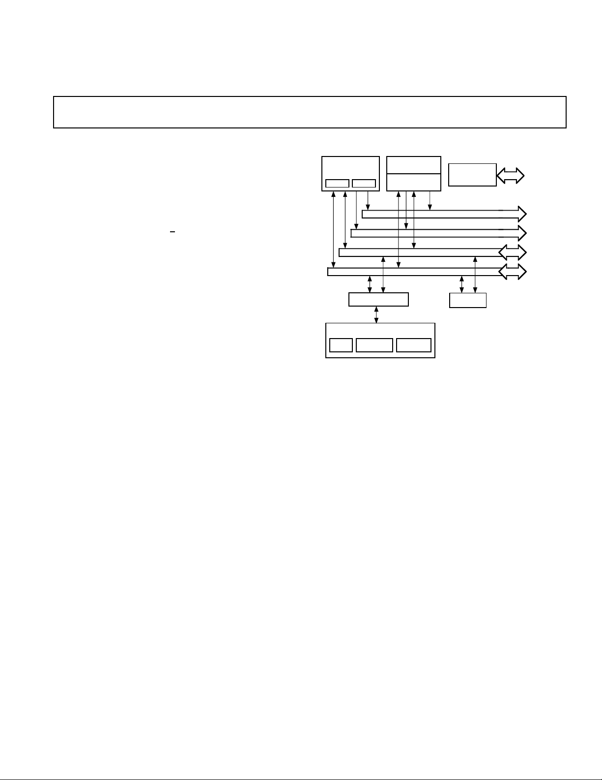
ARCHITECTURE OVERVIEW
Figure 1 shows a block diagram of the ADSP-21020. The
processor features:
Three Computation Units (ALU, Multiplier, and Shifter)
•
with a Shared Data Register File
Two Data Address Generators (DAG 1, DAG 2)
•
Program Sequencer with Instruction Cache
•
32-Bit Timer
•
Memory Buses and Interface
•
JTAG Test Access Port and On-Chip Emulation Support
•
Computation Units
The ADSP-21020 contains three independent computation
units: an ALU, a multiplier with fixed-point accumulator, and a
shifter. In order to meet a wide variety of processing needs, the
computation units process data in three formats: 32-bit
fixed-point, 32-bit floating-point and 40-bit floating-point. The
floating-point operations are single-precision IEEE-compatible
(IEEE Standard 754/854). The 32-bit floating-point format is
EZ-LAB and EZ-ICE are registered trademarks of Analog Devices, Inc.
–2–
REV. C
Page 3
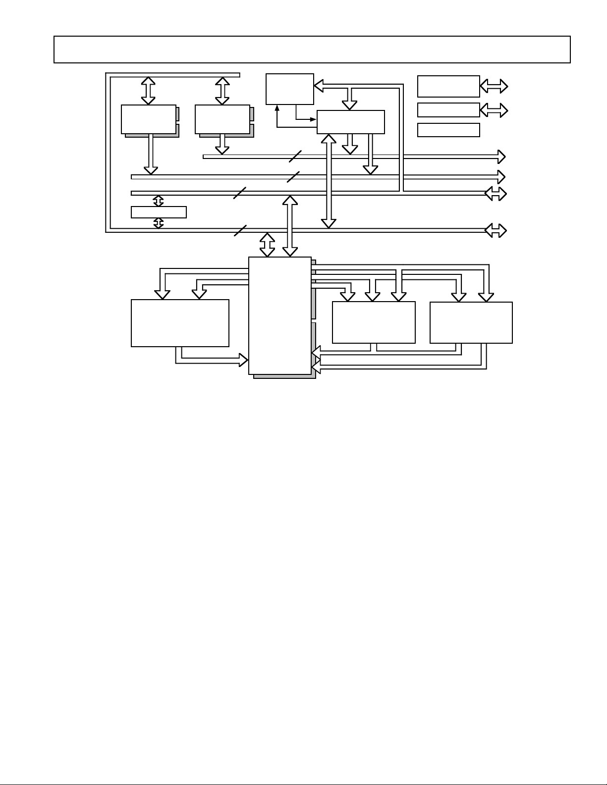
ADSP-21020
DAG 1
8 x 4 x 32
BUS CONNECT
FLOATING & FIXED-POINT
MULTIPLIER, FIXED-POINT
ACCUMULATOR
DAG 2
8 x 4 x 24
PMD BUS
DMD BUS
48
40
PMA BUS
REGISTER
16 x 40
CACHE
MEMORY
32 x 48
24
32DMA BUS
FILE
PROGRAM
SEQUENCER
32-BIT
BARREL
SHIFTER
JTAG TEST &
EMULATION
FLAGS
TIMER
FLOATING-POINT
& FIXED-POINT
PMA
DMA
PMD
DMD
ALU
Figure 1. ADSP-21020 Block Diagram
the standard IEEE format, whereas the 40-bit IEEE extendedprecision format has eight additional LSBs of mantissa for
greater accuracy.
The multiplier performs floating-point and fixed-point
multiplication as well as fixed-point multiply/add and multiply/
subtract operations. Integer products are 64 bits wide, and the
accumulator is 80 bits wide. The ALU performs 45 standard
arithmetic and logic operations, supporting both fixed-point and
floating-point formats. The shifter performs 19 different
operations on 32-bit operands. These operations include logical
and arithmetic shifts, bit manipulation, field deposit, and extract
and derive exponent operations.
The computation units perform single-cycle operations; there is
no computation pipeline. The three units are connected in
parallel rather than serially, via multiple-bus connections with
the 10-port data register file. The output of any computation
unit may be used as the input of any unit on the next cycle. In a
multifunction computation, the ALU and multiplier perform
independent, simultaneous operations.
Data Register File
The ADSP-21020’s general-purpose data register file is used for
transferring data between the computation units and the data
buses, and for storing intermediate results. The register file has
two sets (primary and alternate) of sixteen 40-bit registers each,
for fast context switching.
With a large number of buses connecting the registers to the
computation units, data flow between computation units and
from/to off-chip memory is unconstrained and free from
bottlenecks. The 10-port register file and Harvard architecture
of the ADSP-21020 allow the following nine data transfers to be
performed every cycle:
Off-chip read/write of two operands to or from the register file
•
Two operands supplied to the ALU
•
Two operands supplied to the multiplier
•
Two results received from the ALU and multiplier (three, if
•
the ALU operation is a combined addition/subtraction)
The processor’s 48-bit orthogonal instruction word supports
fully parallel data transfer and arithmetic operations in the same
instruction.
Address Generators and Program Sequencer
Two dedicated address generators and a program sequencer
supply addresses for memory accesses. Because of this, the
computation units need never be used to calculate addresses.
Because of its instruction cache, the ADSP-21020 can
simultaneously fetch an instruction and data values from both
off-chip program memory and off-chip data memory in a single
cycle.
The data address generators (DAGs) provide memory addresses
when external memory data is transferred over the parallel
memory ports to or from internal registers. Dual data address
generators enable the processor to output two simultaneous
addresses for dual operand reads and writes. DAG 1 supplies
32-bit addresses to data memory. DAG 2 supplies 24-bit
addresses to program memory for program memory data
accesses.
Each DAG keeps track of up to eight address pointers, eight
modifiers, eight buffer length values and eight base values. A
pointer used for indirect addressing can be modified by a value
REV. C
–3–
Page 4

ADSP-21020
in a specified register, either before (premodify) or after
(postmodify) the access. To implement automatic modulo
addressing for circular buffers, the ADSP-21020 provides buffer
length registers that can be associated with each pointer. Base
values for pointers allow circular buffers to be placed at arbitrary
locations. Each DAG register has an alternate register that can
be activated for fast context switching.
The program sequencer supplies instruction addresses to
program memory. It controls loop iterations and evaluates
conditional instructions. To execute looped code with zero
overhead, the ADSP-21020 maintains an internal loop counter
and loop stack. No explicit jump or decrement instructions are
required to maintain the loop.
The ADSP-21020 derives its high clock rate from pipelined
fetch, decode and execute cycles. Approximately 70% of the
machine cycle is available for memory accesses; consequently,
ADSP-21020 systems can be built using slower and therefore
less expensive memory chips.
Instruction Cache
The program sequencer includes a high performance, selective
instruction cache that enables three-bus operation for fetching
an instruction and two data values. This two-way, set-associative
cache holds 32 instructions. The cache is selective—only the
instructions whose fetches conflict with program memory data
accesses are cached, so the ADSP-21020 can perform a program
memory data access and can execute the corresponding instruction
in the same cycle. The program sequencer fetches the instruction
from the cache instead of from program memory, enabling the
ADSP-21020 to simultaneously access data in both program
memory and data memory.
Context Switching
Many of the ADSP-21020’s registers have alternate register sets
that can be activated during interrupt servicing to facilitate a fast
context switch. The data registers in the register file, DAG
registers and the multiplier result register all have alternate sets.
Registers active at reset are called primary registers; the others
are called alternate registers. Bits in the MODE1 control register
determine which registers are active at any particular time.
The primary/alternate select bits for each half of the register file
(top eight or bottom eight registers) are independent. Likewise,
the top four and bottom four register sets in each DAG have
independent primary/ alternate select bits. This scheme allows
passing of data between contexts.
Interrupts
The ADSP-21020 has four external hardware interrupts, nine
internally generated interrupts, and eight software interrupts.
For the external interrupts and the internal timer interrupt, the
ADSP-21020 automatically stacks the arithmetic status and
mode (MODE1) registers when servicing the interrupt, allowing
five nesting levels of fast service for these interrupts.
An interrupt can occur at any time while the ADSP-21020 is
executing a program. Internal events that generate interrupts
include arithmetic exceptions, which allow for fast trap handling
and recovery.
Timer
The programmable interval timer provides periodic interrupt
generation. When enabled, the timer decrements a 32-bit count
register every cycle. When this count register reaches zero, the
ADSP-21020 generates an interrupt and asserts its TIMEXP
output. The count register is automatically reloaded from a
32-bit period register and the count resumes immediately.
System Interface
Figure 2 shows an ADSP-21020 basic system configuration.
The external memory interface supports memory-mapped
peripherals and slower memory with a user-defined combination
of programmable wait states and hardware acknowledge signals.
Both the program memory and data memory interfaces support
addressing of page-mode DRAMs.
The ADSP-21020’s internal functions are supported by four
internal buses: the program memory address (PMA) and data
memory address (DMA) buses are used for addresses associated
with program and data memory. The program memory data
(PMD) and data memory data (DMD) buses are used for data
associated with the two memory spaces. These buses are
extended off chip. Four data memory select (DMS) signals
select one of four user-configurable banks of data memory.
Similarly, two program memory select (PMS) signals select
between two user-configurable banks of program memory. All
banks are independently programmable for 0-7 wait states.
The PX registers permit passing data between program memory
and data memory spaces. They provide a bridge between the
48-bit PMD bus and the 40-bit DMD bus or between the 40-bit
register file and the PMD bus.
The PMA bus is 24 bits wide allowing direct access of up to
16M words of mixed instruction code and data. The PMD is 48
bits wide to accommodate the 48-bit instruction width. For
access of 40-bit data the lower 8 bits are unused. For access of
32-bit data the lower 16 bits are ignored.
The DMA bus is 32 bits wide allowing direct access of up to 4
Gigawords of data. The DMD bus is 40 bits wide. For 32-bit
data, the lower 8 bits are unused. The DMD bus provides a
path for the contents of any register in the processor to be
transferred to any other register or to any external data memory
location in a single cycle. The data memory address comes from
one of two sources: an absolute value specified in the instruction
code (direct addressing) or the output of a data address
generator (indirect addressing).
External devices can gain control of the processor’s memory
buses from the ADSP-21020 by means of the bus request/grant
signals (
request, the ADSP-21020 halts internal operations and places
its program and data memory interfaces in a high impedance
state. In addition, three-state controls (
allow an external device to place either the program or data
memory interface in a high impedance state without affecting
the other interface and without halting the ADSP-21020 unless
it requires a memory access from the affected interface. The
three-state controls make it easy for an external cache controller
to hold the ADSP-21020 off the bus while it updates an external
cache memory.
JTAG Test and Emulation Support
The ADSP-21020 implements the boundary scan testing
provisions specified by IEEE Standard 1149.1 of the Joint
Testing Action Group (JTAG). The ADSP-21020’s test
access port and on-chip JTAG circuitry is fully compliant with
the IEEE 1149.1 specification. The test access port enables
boundary scan testing of circuitry connected to the
ADSP-21020’s I/O pins.
BR and BG). To grant its buses in response to a bus
DMTS and PMTS)
–4–
REV. C
Page 5
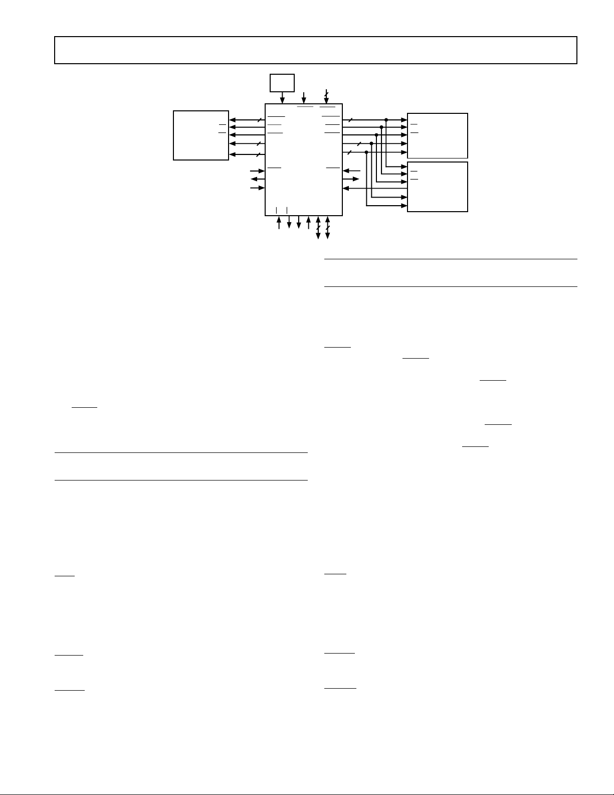
1×
CLOCK
CLKIN
PROGRAM
MEMORY
SELECTS
WE
ADDR
DATA
2
OE
24
48
PMS1-0
PMRD
PMWR
PMA
PMD
ADSP-21010
PMTS
PMACK
BR
BG
RESET
TIMEXP
RCOMP
4
Figure 2. Basic System Configuration
The ADSP-21020 also implements on-chip emulation through
the JTAG test access port. The processor’s eight sets of breakpoint range registers enable program execution at full speed
until reaching a desired break-point address range. The
processor can then halt and allow reading/writing of all the
processor’s internal registers and external memories through the
JTAG port.
PIN DESCRIPTIONS
This section describes the pins of the ADSP-21020. When
groups of pins are identified with subscripts, e.g. PMD
highest numbered pin is the MSB (in this case, PMD
, the
47–0
). Inputs
47
identified as synchronous (S) must meet timing requirements
with respect to CLKIN (or with respect to TCK for TMS, TDI,
and
TRST). Those that are asynchronous (A) can be asserted
asynchronously to CLKIN.
O = Output; I = Input; S = Synchronous; A = Asynchronous;
P = Power Supply; G = Ground.
Pin
Name Type Function
PMA
O Program Memory Address. The ADSP-21020
23–0
outputs an address in program memory on
these pins.
PMD
I/O Program Memory Data. The ADSP-21020
47–0
inputs and outputs data and instructions on
these pins. 32-bit fixed-point data and 32-bit
single-precision floating-point data is transferred over bits 47-16 of the PMD bus.
PMS
O Program Memory Select lines. These pins are
1–0
asserted as chip selects for the corresponding
banks of program memory. Memory banks
must be defined in the memory control
registers. These pins are decoded program
memory address lines and provide an early
indication of a possible bus cycle.
PMRD O Program Memory Read strobe. This pin is
asserted when the ADSP-21020 reads from
program memory.
PMWR O Program Memory Write strobe. This pin is
asserted when the ADSP-21020 writes to
program memory.
PMACK I/S Program Memory Acknowledge. An external
device deasserts this input to add wait states
to a memory access.
ADSP-21020
4
IRQ3-0
4
DMS3-0
DMRD
DMWR
DMTS
DMPAGEPMPAGE
DMACK
FLAG3-0
DMA
DMD
JTAG
5
32
32
Pin
Name Type Function
PMPAGE O Program Memory Page Boundary. The
PMTS I/S Program Memory Three-State Control.
DMA
DMD
DMS
O Data Memory Address. The ADSP-21020
31–0
I/O Data Memory Data. The ADSP-21020
39–0
O Data Memory Select lines. These pins are
3–0
DMRD O Data Memory Read strobe. This pin is
DMWR O Data Memory Write strobe. This pin is
DMACK I/S Data Memory Acknowledge. An external
SELECTS
OE
WE
ADDR
DATA
SELECTS
OE
WE
ACK
ADDR
DATA
DATA
MEMORY
PERIPHERALS
ADSP-21020 asserts this pin to signal that a
program memory page boundary has been
crossed. Memory pages must be defined in
the memory control registers.
PMTS places the program memory address,
data, selects, and strobes in a highimpedance state. If
PMTS is asserted while
a PM access is occurring, the processor will
halt and the memory access will not be
completed. PMACK must be asserted for at
least one cycle when
PMTS is deasserted to
allow any pending memory access to complete properly.
PMTS should only be
asserted (low) during an active memory
access cycle.
outputs an address in data memory on these
pins.
inputs and outputs data on these pins.
32-bit fixed point data and 32-bit
single-precision floating point data is
transferred over bits 39-8 of the DMD bus.
asserted as chip selects for the corresponding banks of data memory. Memory banks
must be defined in the memory control
registers. These pins are decoded data
memory address lines and provide an early
indication of a possible bus cycle.
asserted when the ADSP-21020 reads from
data memory.
asserted when the ADSP-21020 writes to
data memory.
device deasserts this input to add wait states
to a memory access.
REV. C
–5–
Page 6

ADSP-21020
Pin
Name Type Function
DMPAGE O Data Memory Page Boundary. The ADSP-
21020 asserts this pin to signal that a data
memory page boundary has been crossed.
Memory pages must be defined in the
memory control registers.
DMTS I/S Data Memory Three-State Control. DMTS
places the data memory address, data,
selects, and strobes in a high-impedance
state. If
access is occurring, the processor will halt
and the memory access will not be
completed. DMACK must be asserted for
at least one cycle when
deasserted to allow any pending memory
access to complete properly.
only be asserted (low) during an active
memory access cycle.
CLKIIN I External clock input to the ADSP-21020.
The instruction cycle rate is equal to
CLKIN. CLKIN may not be halted,
changed, or operated below the specified
frequency.
RESET I/A Sets the ADSP-21020 to a known state and
begins execution at the program memory
location specified by the hardware reset
vector (address). This input must be
asserted (low) at power-up.
IRQ
3–0
FLAG
BR I/A Bus Request. Used by an external device to
BG O Bus Grant. Acknowledges a bus request
TIMEXP O Timer Expired. Asserted for four cycles
RCOMP Compensation Resistor input. Controls
EVDD P Power supply (for output drivers),
EGND G Power supply return (for output drivers);
I/A Interrupt request lines; may be either edge
triggered or level-sensitive.
I/O/A External Flags. Each is configured via
3–0
control bits as either an input or output. As
an input, it can be tested as a condition. As
an output, it can be used to signal external
peripherals.
request control of the memory interface.
When
execution after completion of the current
cycle, places all memory data, addresses,
selects, and strobes in a high-impedance
state, and asserts
continues normal operation when
released.
(
may take control of the memory interface.
BG is asserted (held low) until BR is
released.
when the value of TCOUNT is
decremented to zero.
compensated output buffers. Connect
RCOMP through a 1.8 kΩ ± 15% resistor
to EVDD. Use of a capacitor (approximately 100 pF), placed in parallel with the
1.8 kΩ resistor is recommended.
nominally +5 V dc (10 pins).
(16 pins).
DMTS is asserted while a DM
DMTS is
DMTS should
BR is asserted, the processor halts
BG. The processor
BR is
BR), indicating that the external device
–6–
Pin
Name Type Function
IVDD P Power supply (for internal circuitry),
nominally +5 V dc (4 pins).
IGND G Power supply return (for internal circuitry); (7
pins).
TCK I Test Clock. Provides an asynchronous clock
for JTAG boundary scan.
TMS I/S Test Mode Select. Used to control the test
state machine. TMS has a 20 kΩ internal
pullup resistor.
TDI VS Test Data Input. Provides serial data for the
boundary scan logic. TDI has a 20 kΩ internal
pullup resistor.
TDO O Test Data Output. Serial scan output of the
boundary scan path.
TRST I/A Test Reset. Resets the test state machine.
TRST must be asserted (pulsed low) after
power-up or held low for proper operation of
the ADSP-21020.
pullup resistor.
NC No Connect. No Connects are reserved pins
that must be left open and unconnected.
INSTRUCTION SET SUMMARY
The ADSP-21020 instruction set provides a wide variety of
programming capabilities. Every instruction assembles into a
single word and can execute in a single processor cycle.
Multifunction instructions enable simultaneous multiplier and
ALU operations, as well as computations executed in parallel
with data transfers. The addressing power of the ADSP-21020
gives you flexibility in moving data both internally and
externally. The ADSP-21020 assembly language uses an
algebraic syntax for ease of coding and readability.
The instruction types are grouped into four categories:
Compute and Move or Modify
Program Flow Control
Immediate Move
Miscellaneous
The instruction types are numbered; there are 22 types. Some
instructions have more than one syntactical form; for example,
Instruction 4 has four distinct forms. The instruction number
itself has no bearing on programming, but corresponds to the
opcode recognized by the ADSP-21020 device.
Because of the width and orthogonality of the instruction word,
there are many possible instructions. For example, the ALU
supports 21 fixed-point operations and 24 floating-point
operations; each of these operations can be the compute portion
of an instruction.
The following pages provide an overview and summary of the
ADSP-21020 instruction set. For complete information, see the
ADSP-21020 User’s Manual. For additional reference information, see the ADSP-21020 Programmer’s Quick Reference.
This section also contains several reference tables for using the
instruction set.
Table I describes the notation and abbreviations used.
•
Table II lists all condition and termination code mnemonics.
•
Table III lists all register mnemonics.
•
Tables IV through VII list the syntax for all compute
•
(ALU, multiplier, shifter or multifunction) operations.
Table VIII lists interrupts and their vector addresses.
•
TRST has a 20 kΩ internal
REV. C
Page 7

COMPUTE AND MOVE OR MODIFY INSTRUCTIONS
1. compute,
2. IF condition compute;
3a. IF condition compute,
3b. IF condition compute,
3c. IF condition compute, ureg =|DM(Ia, Mb)|;
3d. IF condition compute, ureg =|DM(Mb, Ia)|;
4a. IF condition compute,
4b. IF condition compute,
4c. IF condition compute, dreg =|DM(Ia, <data6>)|;
4d. IF condition compute, dreg =|DM(<data6>, Ia)|;
5. IF condition compute, ureg1 = ureg2 ;
6a. IF condition shiftimm,
6b. IF condition shiftimm, dreg = |DM(Ia, Mb)|;
7. IF condition compute, MODIFY |(Ia, Mb)|;
7. IF condition compute, MODIFY
DM(Ia, Mb) = dreg1|,
|
|
dreg1 = DM(Ia, Mb)
DM(Ia, Mb)|= ureg ;
|
|
PM(Ic, Md)
DM(Mb, Ia)|= ureg ;
|
|
PM(Md, Ic)
DM(Ia, <data6>)|= dreg ;
|
|
PM(Ic, <data6>)
DM(<data6>, Ia)|= dreg ;
|
|
PM(<data6>, Ic)
DM(Ia, Mb)| = dreg ;
|
|
PM(Ic, Md)
|
|
|
|
PM(Ic, Md)
|
PM(Md, Ic)
|
PM(Ic, <data6>)
|
PM(<data6>, Ic)
|
PM(Ic, Md)
|
(Ic, Md)
||
|
|
|
|
|
|
|
|
PM(Ic, Md) = dreg2|;
|
dreg2 = PM(Ic, Md)
ADSP-21020
|
PROGRAM FLOW CONTROL INSTRUCTIONS
8. IF condition
9. IF condition
11. IF condition
12. LCNTR =
12. LCNTR =
13. LCNTR =
12. LCNTR =
(DB) Delayed branch
(LA) Loop abort (pop loop PC stacks on branch)
REV. C
JUMP
|
|
CALL
|
|
|
|
|
|
|
|
|
|
|
||
CALL
JUMP
CALL
||
CALL
RTS
|
RTI
|
RTI | (
<data16>| ,DO|<addr24>
ureg
<data16>| , DO|<addr24>
ureg
<addr24>
||
||
(PC, <reladdr6>)
(PC, <reladdr6>)
(Md, Ic)
||
||
(PC, <reladdr6>)
(PC, <reladdr6>)
(|DB,
(|LA,
|
DB, LA
|
,DO
|
,DO
),compute ;
|
|
|
|
(
<PC, <reladdr24>)
|(|
(PC, <reladdr24>)
|
|
|
|
|
|
(|DB
LA
|
(
|
DB, LA
(
(|DB
|
LA
(
|
DB, LA
(
|
(|UNTIL LCE ;
|
) ;
|
|
,
|
),compute ;
|
|
,
|
UNTIL LCE ;
UNTIL termination ;
|
–7–
Page 8

ADSP-21020
IMMEDIATE MOVE INSTRUCTIONS
14a. DM(<addr32>) = ureg ;
PM(<addr24>)
14b. ureg = DM(<addr32>) ;
PM(<addr24>)
15a. DM(<data32>, Ia) = ureg;
PM(< data24>, Ic)
15b. ureg = DM(<data32>, Ia) ;
PM(<data24>, Ic)
16. DM(Ia, Mb) = <data32>;
PM(Ic, Md)
17. ureg = <data32>;
MISCELLANEOUS INSTRUCTIONS
18. BIT SET sreg <data32>;
CLR
TGL
TST
XOR
19a. MODIFY (Ia, <data32>)|;
(Ic, <data32>)|
19b. BITREV (Ia, <data32>) ;
20. |PUSH LOOP , PUSH STS ;
|POP POP
21. NOP ;
22. IDLE ;
Table I. Syntax Notation Conventions
Notation Meaning
UPPERCASE Explicit syntax—assembler keyword (nota-
tion only; assembler is not case-sensitive
and lowercase is the preferred programming
convention)
; Instruction terminator
, Separates parallel operations in an
instruction
italics Optional part of instruction
| between lines | List of options (choose one)
<datan> n-bit immediate data value
<addrn> n-bit immediate address value
<reladdrn> n-bit immediate PC-relative address value
compute ALU, multiplier, shifter or multifunction
operation (from Tables IV-VII)
shiftimm Shifter immediate operation
(from Table VI)
condition Status condition (from Table II)
termination Termination condition (from Table II)
ureg Universal register (from Table III)
sreg System register (from Table III)
dreg R15-R0, F15-F0; register file location
Ia I7-I0; DAG1 index register
Mb M7-M0; DAG1 modify register
Ic I15-I8; DAG2 index register
Md M15-M8; DAG2 modify register
Table II. Condition and Termination Codes
Name Description
eq ALU equal to zero
ne ALU not equal to zero
ge ALU greater than or equal to zero
lt ALU less than zero
le ALU less than or equal to zero
gt ALU greater than zero
ac ALU carry
not ac Not ALU carry
av ALU overflow
not av Not ALU overflow
mv Multiplier overflow
not mv Not multiplier overflow
ms Multiplier sign
not ms Not multiplier sign
sv Shifter overflow
not sv Not shifter overflow
sz Shifter zero
not sz Not shifter zero
flag0_in Flag 0
not flag0_in Not Flag 0
flag1_in Flag 1
not flag1_in Not Flag l
flag2_in Flag 2
not flag2_in Not Flag 2
flag3_in Flag 3
not flag3_in Not Flag 3
tf Bit test flag
not tf Not bit test flag
lce Loop counter expired (DO UNTIL)
not lce Loop counter not expired (IF)
forever Always False (DO UNTIL)
true Always True (IF)
In a conditional instruction, the execution of the entire instruction is based on
the specified condition.
–8–
REV. C
Page 9

ADSP-21020
Table III. Universal Registers
Name Function
Register File
R15–R0 Register file locations
Program Sequencer
PC* Program counter; address of instruction cur-
rently executing
PCSTK Top of PC stack
PCSTKP PC stack pointer
FADDR* Fetch address
DADDR* Decode address
LADDR Loop termination address, code; top of loop
address stack
CURLCNTR Current loop counter; top of loop count stack
LCNTR Loop count for next nested counter-controlled
loop
Data Address Generators
I7–I0 DAG1 index registers
M7–M0 DAG1 modify registers
L7–L0 DAG1 length registers
B7–B0 DAG1 base registers
I15–I8 DAG2 index registers
M15–M8 DAG2 modify registers
L15–L8 DAG2 length registers
B15–B8 DAG2 base registers
Bus Exchange
PX1 PMD-DMD bus exchange 1 (16 bits)
PX2 PMD-DMD bus exchange 2 (32 bits)
PX 48-bit PX1 and PX2 combination
Timer
TPERIOD Timer period
TCOUNT Timer counter
Memory Interface
DMWAIT Wait state and page size control for data
memory
DMBANK1 Data memory bank 1 upper boundary
DMBANK2 Data memory bank 2 upper boundary
DMBANK3 Data memory bank 3 upper boundary
DMADR* Copy of last data memory address
PMWAIT Wait state and page size control for program
memory
PMBANK1 Program memory bank 1 upper boundary
PMADR* Copy of last program memory address
System Registers
MODE1 Mode control bits for bit-reverse, alternate reg-
isters, interrupt nesting and enable, ALU satu-
ration, floating-point rounding mode and
boundary
MODE2 Mode control bits for interrupt sensitivity,
cache disable and freeze, timer enable, and I/O
flag configuration
IRPTL Interrupt latch
IMASK Interrupt mask
IMASKP Interrupt mask pointer (for nesting)
ASTAT Arithmetic status flags, bit test, I/O flag values,
and compare accumulator
STKY Sticky arithmetic status flags, circular buffer
overflow flags, stack status flags (not sticky)
USTAT1 User status register l
USTAT2 User status register 2
*read-only
Refer to User’s Manual for bit-level definitions of each register.
Table IV. ALU Compute Operations
Fixed-Point Floating-Point
Rn = Rx + Ry Fn = Fx + Fy
Rn = Rx – Ry Fn = Fx – Fy
Rn = Rx + Ry, Rm = Rx – Ry Fn = Fx + Fy, Fm = Fx – Fy
Rn = Rx + Ry + CI Fn = ABS (Fx + Fy)
Rn = Rx – Ry + CI – l Fn = ABS (Fx – Fy)
Rn = (Rx + Ry)/2 Fn = (Fx + Fy)/2
COMP(Rx, Ry) COMP(Fx, Fy)
Rn = –Rx Fn = –Fx
Rn = ABS Rx Fn = ABS Fx
Rn = PASS Rx Fn = PASS Fx
Rn = MIN(Rx, Ry) Fn = MIN(Fx, Fy)
Rn = MAX(Rx, Ry) Fn = MAX(Fx, Fy)
Rn = CLIP Rx BY Ry Fn = CLIP Fx BY Fy
Rn = Rx + CI Fn = RND Fx
Rn = Rx + CI – 1 Fn = SCALB Fx BY Ry
Rn = Rx + l Rn = MANT Fx
Rn = Rx – l Rn = LOGB Fx
Rn = Rx AND Ry Rn = FIX Fx BY Ry
Rn = Rx OR Ry Rn = FIX Fx
Rn = Rx XOR Ry Fn = FLOAT Rx BY Ry
Rn = NOT Rx Fn = FLOAT Rx
Fn = RECIPS Fx
Fn = RSQRTS Fx
Fn = Fx COPYSIGN Fy
Rn, Rx, Ry R15–R0; register file location, fixed-point
Fn, Fx, Fy F15–F0; register file location, floating point
REV. C
–9–
Page 10

ADSP-21020
Table V. Multiplier Compute Operations
Rn = Rx * Ry ( SSF ) Fn = Fx * Fy
MRF = Rx * Ry ( UUI
MRB = Rx * Ry (U U FR
Rn = MRF + Rx * Ry ( SSF ) Rn = MRF – Rx * Ry ( SSF )
Rn = MRB + Rx * Ry ( UUI Rn = MRB= Rx * Ry ( UUI
MRF = MRF + Rx * Ry ( U U FR MRF = MRF= Rx * Ry ( UUI FR
MRB = MRB MRB = MRB
Rn = SAT MRF (SI) Rn = RND MRF (SF)
Rn = SAT MRB (UI) Rn = RND MRB (UF)
MRF = SAT MRF (SF) MRF = RND MRF
MRB = SAT MRB (UF) MRB = RND MRB
MRF = 0
MRB
MRxF = Rn Rn = MRxF
MRxB Rn = MRxB
Rn, Rx, Ry R15–R0; register file location, fixed-point
Fn, Fx, Fy F15–F0; register file location, floating-point
MRxF MR2F, MR1F; MR0F; multiplier result accumulators, foreground
MRxB MR2B, MR1B, MR0B; multiplier result accumulators, background
( x-input y-input data format, )
( x-input y-input rounding
S Signed input
U Unsigned input
I Integer input(s)
F Fractional input(s)
FR Fractional inputs, Rounded output
(SF) Default format for 1-input operations
(SSF) Default format for 2-input operations
Table VI. Shifter and Shifter Immediate Compute Operations
Shifter Shifter Immediate
Rn = LSHIFT Rx BY Ry Rn = LSHIFT Rx BY<data8>
Rn = Rn OR LSHIFT Rx BY Ry Rn = Rn OR LSHIFT Rx BY<data8>
Rn = ASHIFT Rx BY Ry Rn = ASHIFT Rx BY<data8>
Rn = Rn OR ASHIFT Rx BY Ry Rn = Rn OR ASHIFT Rx BY<data8>
Rn = ROT Rx BY RY Rn = ROT Rx BY<data8>
Rn = BCLR Rx BY Ry Rn = BCLR Rx BY<data8>
Rn = BSET Rx BY Ry Rn = BSET Rx BY<data8>
Rn = BTGL Rx BY Ry Rn = BTGL Rx BY<data8>
BTST Rx BY Ry BTST Rx BY<data8>
Rn = FDEP Rx BY Ry Rn = FDEP Rx BY <bit6>: <len6>
Rn = Rn OR FDEP Rx BY Ry Rn = Rn OR FDEP Rx BY <bit6>:<1en6>
Rn = FDEP Rx BY Ry (SE) Rn = FDEP Rx BY <bit6>:<1en6> (SE)
Rn = Rn OR FDEP Rx BY Ry (SE) Rn = Rn OR FDEP Rx BY <bit6>:<1en6> (SE)
Rn = FEXT Rx BY Ry Rn = FEXT Rx BY <bit6>:<1en6>
Rn = FEXT Rx BY Ry (SE) Rn = FEXT Rx BY <bit6>:<1en6> (SE)
Rn = EXP Rx
Rn = EXP Rx (EX)
Rn = LEFTZ Rx
Rn = LEFTO Rx
Rn, Rx, Ry R15-R0; register file location, fixed-point
<bit6>:<len6> 6-bit immediate bit position and length values (for shifter immediate operations)
–10–
REV. C
Page 11

ADSP-21020
Table Vll. Multifunction Compute Operations
Fixed-Point
Rm=R3-0 * R7-4 (SSFR), Ra=R11-8 + R15-12
Rm=R3-0 * R7-4 (SSFR), Ra=R11-8 – R15-12
Rm=R3-0 * R7-4 (SSFR), Ra=(R11-8 + R15-12)/2
MRF=MRF + R3-0 * R7-4 (SSF), Ra=R11-8 + R15-12
MRF=MRF + R3-0 * R7-4 (SSF), Ra=R11-8 – R15-12
MRF=MRF + R3-0 * R7-4 (SSF), Ra=(R11-8 + R15-12)/2
Rm=MRF + R3-0 * R7-4 (SSFR), Ra=R11-8 + R15-12
Rm=MRF + R3-0 * R7-4 (SSFR), Ra=R11-8 – R15-12
Rm=MRF + R3-0 * R7-4 (SSFR), Ra=(R11-8 + R15-12)/2
MRF=MRF – R3-0 * R7-4 (SSF), Ra=R11-8 + R15-12
MRF=MRF – R3-0 * R7-4 (SSF), Ra=R11-8 – R15-12
MRF=MRF – R3-0 * R7-4 (SSF), Ra=(R11-8 + R15-12)/2
Rm=MRF – R3-0 * R7-4 (SSFR), Ra=R11-8 + R15-12
Rm=MRF – R3-0 * R7-4 (SSFR), Ra=R11-8 – R15-12
Rm=MRF – R3-0 * R7-4 (SSFR), Ra=(R11-8 + R15-12)/2
Rm=R3-0 * R7-4 (SSFR), Ra=R11-8 + R15-12,
Rs=R11-8 – R15-12
Floating-Point
Fm=F3-0 * F7-4, Fa=F11-8 + F15-12
Fm=F3-0 * F7-4, Fa=F11-8 – F15-12
Fm=F3-0 * F7-4, Fa=FLOAT R11-8 by R15-12
Fm=F3-0 * F7-4, Fa=FIX R11-8 by R15-12
Fm=F3-0 * F7-4, Fa=(F11-8 + F15-12)/2
Fm=F3-0 * F7-4, Fa=ABS F11-8
Fm=F3-0 * F7-4, Fa=MAX (F11-8, F15-12)
Fm=F3-0 * F7-4, Fa=MIN (F11-8, F15-12)
Fm=F3-0 * F7-4, Fa=F11-8 + F15-12,
Fs=F11-8 – F15-12
Table VIII. Interrupt Vector Addresses and Priorities
Vector
Address
No. (Hex) Function
0 0x00 Reserved
1* 0x08 Reset
2 0xl0 Reserved
3 0xl8 Status stack or loop stack overflow or
PC stack full
4 0x20 Timer=0 (high priority option)
5 0x28
6 0x30
7 0x38
8 0x40
IRQ3 asserted
IRQ2 asserted
IRQ1 asserted
IRQ0 asserted
9 0x48 Reserved
10 0x50 Reserved
11 0x58 DAG 1 circular buffer 7 overflow
12 0x60 DAG 2 circular buffer 15 overflow
13 0x68 Reserved
14 0x70 Timer=0 (low priority option)
15 0x78 Fixed-point overflow
16 0x80 Floating-point overflow
17 0x88 Floating-point underflow
18 0x90 Floating-point invalid operation
19–23 0x98-0xB8 Reserved
24–31 0xC0–OxF8 User software interrupts
*Nonmaskable
Ra, Rm Any register file location (fixed-point)
R3-0 R3, R2, R1, R0
R7-4 R7, R6, R5, R4
R11-8 R11, R10, R9, R8
R15-12 R15, R14, R13, R12
Fa, Fm Any register file location (floating-point)
F3-0 F3, F2, F1, F0
F7-4 F7, F6, F5, F4
F11-8 F11, F10, F9, F8
F15-12 F15, F14, F13, F12
(SSF) X-input signed, Y-input signed, fractional inputs
(SSFR) X-input signed, Y-input signed, fractional inputs, rounded output
REV. C
–11–
Page 12

ADSP-21020–SPECIFICATIONS
WARNING!
ESD SENSITIVE DEVICE
RECOMMENDED OPERATING CONDITIONS
K Grade B Grade T Grade
Parameter Min Max Min Max Min Max Unit
V
DD
T
AMB
Refer to Environmental Conditions for information on thermal specifications.
Supply Voltage 4.50 5.50 4.50 5.50 4.50 5.50 V
Ambient Operating Temperature 0 +70 –40 +85 –55 +125 °C
ELECTRICAL CHARACTERISTICS
Parameter Test Conditions Min Max Unit
9, 10
1
2, 12
1, 12
2
3, 11
3, 11
4, 5
4
5
6
6
7
8
VDD = max 2.0 V
VDD = max 3.0 V
VDD = min 0.8 V
VDD = max 0.6 V
VDD = min, IOH = –1.0 mA 2.4 V
VDD = min, IOL = 4.0 mA 0.4 V
VDD = max, VIN = V
VDD = max, V
VDD = max, V
VDD = max, VIN = V
VDD = max, V
tCK = 30–33 ns, VDD = max, V
V
= 2.4 V, VIL = V
IH
VDD = max, VIN = 0 V or VDD max 150 mA
fIN = 1 MHz, T
(typical) = 230 mA; at tCK = 40 ns, I
DDIN
max 10 µA
DD
= 0 V 10 µA
IN
= 0 V 350 µA
IN
IN
max 10 µA
DD
= 0 V 10 µA
= 3.0 V, 490 mA
IHCR
= 0.4 V
ILC
= 25°C, V
CASE
DDIN
= 2.5 V 10 pF
IN
(max) = 420 mA and I
(typical) = 200 mA; at tCK = 50 ns,
DDIN
V
IH
V
IHCR
V
IL
V
ILC
V
OH
V
OL
I
IH
I
IL
I
ILT
I
OZH
I
OZL
I
DDIN
I
DDIDLE
C
IN
NOTES
l
Applies to: PMD47–0, PMACK, PMTS, DMD39–0, DMACK, DMTS, IRQ3–0. FLAG3–0, BR, TMS, TDI.
2
Applies to: CLKIN, TCK.
3
Applies to: PMA23–0, PMD47–0, PMS1–0, PMRD, PMWR, PMPAGE, DMA31–0, DMD39–0, DMS3–0, DMRD, DMWR, DMPAGE, FLAG3–0,
TIMEXP, BG.
4
Applies to: PMACK, PMTS, DMACK, DMTS, IRQ3–0, BR, CLKIN, RESET, TCK.
5
Applies to: TMS, TDI, TRST.
6
Applies to: PMA23–0, PMD47–0, PMS1–0, PMRD, PMWR, PMPAGE, DMA31–0, DMD39–0, DMS3–0, DMRD, DMWR, DMPAGE, FLAG3–0, TDO.
7
Applies to IVDD pins. At tCK = 30–33 ns, I
I
DDIN
8
Applies to IVDD pins. Idle refers to ADSP-21020 state of operation during execution of the IDLE instruction.
9
Guaranteed but not tested.
10
Applies to all signal pins.
11
Although specified for TTL outputs, all ADSP-21020 outputs are CMOS-compatible and will drive to VDD and GND assuming no dc loads.
12
Applies to RESET, TRST.
Hi-Level Input Voltage
Hi-Level Input Voltage
Lo-Level Input Voltage
Lo-Level Input Voltage
Hi-Level Output Voltage
Lo-Level Output Voltage
Hi-Level Input Current
Lo-Level Input Current
Lo-Level Input Current
Tristate Leakage Current
Tristate Leakage Current
Supply Current (Internal)
Supply Current (Idle)
Input Capacitance
(max) = 370 mA and I
(typical) = 115 mA. See “Power Dissipation” for calculation of external (EVDD) supply current for total supply current.
DDIN
ABSOLUTE MAXIMUM RATINGS*
Supply Voltage . . . . . . . . . . . . . . . . . . . . . . . . . –0.3 V to +7 V
Input Voltage . . . . . . . . . . . . . . . . . . . . –0.3 V to V
Output Voltage Swing . . . . . . . . . . . . . –0.3 V to V
+ 0.3 V
DD
+ 0.3 V
DD
Load Capacitance . . . . . . . . . . . . . . . . . . . . . . . . . . . . 200 pF
*Stresses above those listed under “Absolute Maximum Ratings” may cause
permanent damage to the device. These are stress ratings only and functional
operation of the device at these or any other conditions above those indicated in the
operational sections of this specification is not implied. Exposure to absolute
maximum rating conditions for extended periods may affect device reliability.
Operating Temperature Range (Ambient) . . –55°C to +125°C
Storage Temperature Range . . . . . . . . . . . . –65°C to +150°C
Lead Temperature (10 seconds) CPGA . . . . . . . . . . . +300°C
ESD SENSITIVITY
The ADSP-21020 features proprietary input protection circuitry to dissipate high energy discharges
(Human Body Model). Per method 3015 of MIL-STD-883, the ADSP-21020 has been classified
as a Class 3 device, with the ability to withstand up to 4000 V ESD.
Proper ESD precautions are strongly recommended to avoid functional damage or performance
degradation. Charges readily accumulate on the human body and test equipment and discharge
without detection. Unused devices must be stored in conductive foam or shunts, and the foam
should be discharged to the destination socket before devices are removed. For further information
on ESD precautions, refer to Analog Devices’ ESD Prevention Manual.
–12–
REV. C
Page 13

ADSP-21020
TIMING PARAMETERS
General Notes
See Figure 15 on page 24 for voltage reference levels. Use the exact timing information given. Do not attempt to derive parameters
from the addition or subtraction of others. While addition or subtraction would yield meaningful results for an individual device, the
values given in this data sheet reflect statistical variations and worst cases. Consequently, you cannot meaningfully add parameters to
derive other specifications.
Clock Signal
K/B/T Grade K/B/T Grade B/T Grade K Grade
20 MHz 25 MHz 30 MHz 33.3 MHz
Parameter Min Max Min Max Min Max Min Max Unit
Timing Requirement:
t
CK
t
CKH
t
CKL
CLKIN Period 50 150 40 150 33 150 30 150 ns
CLKIN Width High 10 10 10 10 ns
CLKIN Width Low 10 10 10 10 ns
t
CK
CLKIN
t
CKH
t
CKL
Figure 3. Clock
Reset
K/B/T Grade K/B/T Grade B/T Grade K Grade
20 MHz 25 MHz 30 MHz 33.3 MHz Frequency Dependency*
Parameter Min Max Min Max Min Max Min Max Min Max Unit
Timing Requirement:
1
t
RESET Width Low 200 160 132 120 4t
WRST
2
t
RESET Setup before CLKIN High 29 50 24 40 21 33 19 30 29 + DT/2 30 ns
SRST
NOTES
DT = tCK –50 ns
1
Applies after the power-up sequence is complete. At power up, the Internal Phase Locked Loop requires no more than 1000 CLKIN cycles while RESET is low,
assuming stable VDD and CLKIN (not including clock oscillator start-up time).
2
Specification only applies in cases where multiple ADSP-21020 processors are required to execute in program counter lock-step (all processors start execution at
location 8 in the same cycle). See the Hardware Configuration chapter of the ADSP-21020 User’s Manual for reset sequence information.
CLKIN
RESET
t
WRST
t
SRST
CK
ns
Figure 4. Reset
REV. C
–13–
Page 14

ADSP-21020
Interrupts
K/B/T Grade K/B/T Grade B/T Grade K Grade
20 MHz 25 MHz 30 MHz 33.3 MHz Frequency Dependency*
Parameter Min Max Min Max Min Max Min Max Min Max Unit
Timing Requirement:
t
IRQ3-0 Setup before CLKIN High 38 31 25 23 38 + 3DT/4 ns
SIR
t
IRQ3-0 Hold after CLKIN High 0 0 0 0 ns
HIR
t
IRQ3-0 Pulse Width 55 45 38 35 tCK + 5 ns
IPW
NOTE
*DT = tCK – 50 ns
Meeting setup and hold guarantees interrupts will be latched in that cycle. Meeting the pulse width is not necessary if the setup and hold is met. Likewise, meeting the
setup and hold is not necessary if the pulse width is met. See the Hardware Configuration chapter of the ADSP-21020 User’s Manual for interrupt servicing information.
CLKIN
t
HIR
IRQ3-0
t
SIR
t
IPW
Figure 5. Interrupts
Timer
K/B/T Grade K/B/T Grade B/T Grade K Grade
20 MHz 25 MHz 30 MHz 33.3 MHz Frequency Dependency*
Parameter Min Max Min Max Min Max Min Max Min Max Unit
Switching Characteristic:
t
CLKIN High to TIMEXP 24 24 24 24 ns
DTEX
NOTE
*DT = tCK – 50 ns
CLKIN
TIMEXP
t
DTEX
t
DTEX
Figure 6. TIMEXP
–14–
REV. C
Page 15

ADSP-21020
Flags
K/B/T Grade K/B/T Grade B/T Grade K Grade
20 MHz 25 MHz 30 MHz 33.3 MHz Frequency Dependency*
Parameter Min Max Min Max Min Max Min Max Min Max Unit
Timing Requirement:
t
FLAG3-0IN Setup before CLKIN High 19 16 14 13 19 + 5DT/16 ns
SFI
FLAG3-0IN Hold after CLKIN High 0 0 0 0 ns
t
HFI
FLAG3-0IN Delay from xRD, xWR Low 12 8 5 3 12 + 7DT/16 ns
t
DWRFI
t
FLAG3-0IN Hold after xRD, xWR 0000 ns
HFIWR
Deasserted
Switching Characteristic:
t
FLAG3-0
DFO
FLAG3-0
t
HFO
CLKIN High to FLAG3-0
t
DFOE
t
CLKIN High to FLAG3-0
DFOD
NOTES
*DT = tCK – 50 ns
1
Flag inputs meeting these setup and hold times will affect conditional operations in the next instruction cycle. See the Hardware Configuration chapter of the
ADSP-21020 User’s Manual for additional flag servicing information.
x = PM or DM.
1
Delay from CLKIN High 24 24 24 24 ns
OUT
Hold after CLKIN High 5 5 5 5 ns
OUT
Enable 1 1 1 1 ns
OUT
Disable 24 24 24 24 ns
OUT
FLAG3-0
FLAG3-0
xRD, xWR
CLKIN
OUT
CLKIN
t
t
t
DFOE
t
SFI
IN
t
DWRFI
FLAG INPUT
DFO
FLAG OUTPUT
t
HFI
t
HFIWR
t
DFO
HFO
t
DFOD
Figure 7. Flags
REV. C
–15–
Page 16

ADSP-21020
Bus Request/Bus Grant
K/B/T Grade K/B/T Grade B/T Grade K Grade
20 MHz 25 MHz 30 MHz 33.3 MHz Frequency Dependency*
Parameter Min Max Min Max Min Max Min Max Min Max Unit
Timing Requirement:
t
HBR
t
SBR
Switching Characteristic:
t
DMDBGL
t
DME
t
DBGL
t
DBGH
NOTES
*DT = tCK – 50 ns.
Memory Interface = PMA23-0, PMD47-0, PMS1-0, PMRD, PMWR, PMPAGE, DMA31-0, DMD39-0, DMS3-0, DMRD, DMWR, DMPAGE.
Buses are not granted until completion of current memory access.
See the Memory Interface chapter of the ADSP-21020 User’s Manual for BG, BR cycle relationships.
BR Hold after CLKIN High 0 0 0 0 ns
BR Setup before CLKIN High 18 15 13 12 18 + 5DT/16 ns
Memory Interface Disable to BG Low –2 –2 –2 –2 ns
CLKIN High to Memory Interface
Enable 25 20 16 15 25 + DT/2 ns
CLKIN High to BG Low 22 22 22 22 ns
CLKIN High to BG High 22 22 22 22 ns
CLKIN
BR
MEMORY
INTERFACE
BG
t
HBR
t
SBR
t
DBGL
t
DMDBGL
t
HBR
t
SBR
t
DME
t
DBGH
Figure 8. Bus Request/Bus Grant
–16–
REV. C
Page 17

ADSP-21020
External Memory Three-State Control
K/B/T Grade K/B/T Grade B/T Grade K Grade
20 MHz 25 MHz 30 MHz 33.3 MHz Frequency Dependency*
Parameter Min Max Min Max Min Max Min Max Min Max Unit
Timing Requirement:
t
xTS, Setup before CLKIN High 14 50 12 40 10 33 9 30 14 + DT/4 t
STS
t
DADTS
t
DSTS
xTS Delay after Address, Select 28 19 13 10 28 + 7DT/8 ns
xTS Delay after XRD, XWR Low 16 11 7 6 16 + DT/2 ns
CK
Switching Characteristic:
Memory Interface Disable before
t
DTSD
CLKIN High 0 –2 –4 –5 DT/4 ns
t
xTS High to Address, Select Enable 0 0 0 0 ns
DTSAE
NOTES
*DT = tCK – 50 ns.
xTS should only be asserted (low) during an active memory access cycle.
Memory Interface = PMA23-0, PMD47-0, PMS1-0, PMRD, PMWR, PMPAGE, DMA31-0, DMD39-0, DMS3-0, DMRD, DMWR, DMPAGE.
Address = PMA23-0, DMA31-0. Select = PMS1-0, DMS3-0.
x = PM or DM.
CLKIN
ns
PMTS, DMTS
xRD, xWR
ADDRESS,
SELECTS
DATA
t
STS
t
DADTS
t
DSTS
t
DTSD
t
DTSAE
Figure 9. External Memory Three-State Control
t
STS
REV. C
–17–
Page 18

ADSP-21020
Memory Read
K/B/T Grade K/B/T Grade B/T Grade K Grade
20 MHz 25 MHz 30 MHz 33.3 MHz Frequency Dependence*
Parameter Min Max Min Max Min Max Min Max Min Max Unit
Timing Requirement:
t
Address, Select to Data Valid 37 27 20 17 37 + DT ns
DAD
xRD Low to Data Valid 24 18 13 11 24 + 5DT/8 ns
t
DRLD
Data Hold from Address, Select 0 0 0 0 ns
t
HDA
t
Data Hold from xRD High –1 –1 –1 –1 ns
HDRH
xACK Delay from Address 27 18 12 9 27 + 7DT/8 ns
t
DAAK
xACK Delay from xRD Low 15 10 6 5 15 + DT/2 ns
t
DRAK
t
xACK Setup before CLKIN High 14 12 10 9 14 + DT/4 ns
SAK
xACK Hold after CLKIN High 0 0 0 0 ns
t
HAK
Switching Characteristic:
t
Address, Select to xRD Low 8 4 2 0 8 + 3DT/8 ns
DARL
xPAGE Delay from Address, Select 1 1 1 1 ns
t
DAP
CLKIN High to xRD Low 16 26 13 24 12 22 11 21 16 + DT/4 26 + DT/4 ns
t
DCKRL
t
xRD Pulse Width 26 20 15 13 26 + 5DT/8 ns
RW
t
xRD High to xRD, xWD Low 17 13 11 9 17 + 3DT/8
RWR
NOTES
*DT = tCK – 50 ns
x = PM or DM; Address = PMA23-0, DMA31-0; Data = PMD47-0, DMD39-0; Select = PMS1-0, DMS3-0.
ns
–18–
REV. C
Page 19

CLKIN
ADDRESS,
SELECT
DMPAGE,
PMPAGE
DMRD,
PMRD
DATA
DMACK,
PMACK
DMWR,
PMWR
t
DAP
t
DCKRL
t
DARL
t
DAAK
t
DRAK
t
DAD
t
DRLD
ADSP-21020
t
RW
t
HDA
t
HDRH
t
t
SAK
t
HAK
RWR
Figure 10. Memory Read
REV. C
–19–
Page 20

ADSP-21020
Memory Write
K/B/T Grade K/B/T Grade B/T Grade K Grade
20 MHz 25 MHz 30 MHz 33.3 MHz Frequency Dependency*
Parameter Min Max Min Max Min Max Min Max Min Max Unit
Timing Requirement: 12
t
xACK Delay from Address, Select 27 18 6 9 27 + 7DT/8 ns
DAAK
xACK Delay from xWR Low 15 10 10 5 15 + DT/2 ns
t
DWAK
xACK Setup before CLKIN High 14 12 0 9 14 + DT/4 ns
t
SAK
t
xACK Hold after CLKIN High 0 0 0 ns
HAK
Switching Characteristic:
t
Address, Select to xWR Deasserted 37 28 21 18 37+ 15DT/16 ns
DAWH
t
Address, Select to xWR Low 11 7 5 3 11 + 3DT/8 ns
DAWL
xWR Pulse Width 26 20 16 15 26 + 9DT/16 ns
t
WW
Data Setup before xWR High 23 18 14 13 23 + DT/2 ns
t
DDWH
t
Address, Select Hold after xWR
DWHA
Deasserted 1 0 0 0 1 + DT/16 ns
Data Hold after xWR Deasserted10 –1 –1 –1 DT/16 ns
t
HDWH
t
xPAGE Delay from Address, Select 1 1 1 1 ns
DAP
CLKIN High to xWR Low 16 26 13 24 12 22 11 21 16 + DT/4 26 + DT/4 ns
t
DCKWL
xWR High to xWR or xRD Low 17 13 10 8 17 + 7DT/16 ns
t
WWR
t
Data Disable before xWR or xRD
DDWR
Low 13 9 7 5 13 + 3DT/8 ns
t
xWR Low to Data Enabled 0 –1 –1 –1 DT/16 ns
WDE
NOTES
*DT = tC – 50 ns
See “System Hold Time Calculation” in “Test Conditions” section for calculating hold times given capacitive and DC loads.
x = PM or DM; Address = PMA23-0, DMA31-0; Data = PMD47-0, DMD39-0; Select = PMS1-0, DMS3-0.
–20–
REV. C
Page 21

CLKIN
ADDRESS,
SELECT
DMPAGE,
PMPAGE
DMWR,
PMWR
t
DAP
t
DCKWL
t
DAWL
t
WDE
t
DAWH
t
WW
t
DDWH
t
DWHA
ADSP-21020
t
WWR
t
HDWH
DATA
DMACK,
PMACK
DMRD,
PMRD
t
DAAK
t
DWAK
t
SAK
Figure 11. Memory Write
t
HAK
t
DDWR
REV. C
–21–
Page 22

ADSP-21020
IEEE 1149.1 Test Access Port
K/B/T Grade K/B/T Grade B/T Grade K Grade
20 MHz 25 MHz 30 MHz 33.3 MHz Frequency Dependency*
Parameter Min Max Min Max Min Max Min Max Min Max Unit
Timing Requirement:
t
TCK Period 50 40 33 30 t
TCK
TDI, TMS Setup before TCK High 5 5 5 5 ns
t
STAP
t
TDI, TMS Hold after TCK High 6 6 6 6 ns
HTAP
System Inputs Setup before TCK High 7 7 7 7 ns
t
SSYS
System Inputs Hold after TCK High 9 9 9 9 ns
t
HSYS
t
TRST Pulse Width 200 160 132 120 ns
TRSTW
CK
Switching Characteristic:
t
TDO Delay from TCK Low 15 15 15 15 ns
DTDO
t
System Outputs Delay from TCK Low 26 26 26 26 ns
DSYS
NOTES
*DT = tC – 50 ns
System Inputs = PMD47-0, PMACK, PMTS, DMD39-0, DMACK, DMTS, CLKIN, IRQ3 0, RESET, FLAG3-0, BR.
System Outputs = PMA23-0, PMS1-0, PMRD, PMWR, PMD47-0, PMPAGE, DMA31-0, DMS1-0, DMRD, DMWR, DMD39-0, DMPAGE, FLAG3-0, BG,
TIMEXP.
See the IEEE 1149.1 Test Access Port chapter of the ADSP-21020 User’s Manual for further detail.
ns
–22–
REV. C
Page 23

TCK
t
ADSP-21020
TCK
TMS,TDI
TDO
SYSTEM
INPUTS
SYSTEM
OUTPUTS
t
SSYS
t
STAP
t
HTAP
t
DTDO
t
HSYS
t
DSYS
Figure 12. IEEE 1149.1 Test Access Port
REV. C
–23–
Page 24

ADSP-21020
TO
OUTPUT
PIN
50pF
*
+1.5V
*
AC TIMING SPECIFICATIONS ARE CALCULATED FOR 100pF
DERATING ON THE FOLLOWING PINS: PMA23–0, PMS1–0, PMRD,
PMWR, PMPAGE, DMA31–0, DMS3–0, DMRD, DMWR, DMPAGE
I
OH
I
OL
TEST CONDITIONS
Output Disable Time
Output pins are considered to be disabled when they stop
driving, go into a high-impedance state, and start to decay from
their output high or low voltage. The time for the voltage on the
bus to decay by ∆V is dependent on the capacitive load, C
the load current, I
. It can be approximated by the following
L
equation:
∆V
C
t
DECAY
The output disable time (t
t
MEASURED
t
MEASURED
and t
as shown in Figure 13. The time
DECAY
) is the interval from when the reference signal
DIS
L
=
I
L
) is the difference between
switches to when the output voltage decays ∆V from the
measured output high or output low voltage. t
calculated with ∆V equal to 0.5 V, and test loads C
DECAY
L
Output Enable Time
Output pins are considered to be enabled when they have made
a transition from a high-impedance state to when they start
driving. The output enable time (t
) is the interval from when
ENA
a reference signal reaches a high or low voltage level to when the
output has reached a specified high or low trip point, as shown
in the Output Enable/Disable diagram. If multiple pins (such as
the data bus) are enabled, the measurement value is that of the
first pin to start driving.
Example System Hold Time Calculation
To determine the data output hold time in a particular system,
first calculate t
using the above equation. Choose ∆V to be
DECAY
the difference between the ADSP-21020’s output voltage and
the input threshold for the device requiring the hold time. A
typical ∆V will be 0.4 V. C
data line), and I
is the total leakage or three-state current (per
L
data line). The hold time will be t
disable time (i.e. t
HDWD
is the total bus capacitance (per
L
plus the minimum
DECAY
for the write cycle).
is
and IL.
, and
L
Figure 14. Equivalent Device Loading For AC
Measurements (Includes All Fixtures)
INPUT OR
OUTPUT
1.5V
1.5V
Figure 15. Voltage Reference Levels For AC
Measurements (Except Output Enable/Disable)
REFERENCE
SIGNAL
t
DIS
V
OH (MEASURED)
OUTPUT
V
OL (MEASURED)
OUTPUT STOPS DRIVING
t
DECAY
t
MEASURED
V
OH (MEASURED)
V
OL (MEASURED)
HIGH-IMPEDANCE STATE. TEST CONDITIONS
CAUSE THIS VOLTAGE LEVEL TO BE
APPROXIMATELY 1.5 V.
–∆V
+∆V
2.0V
1.0V
Figure 13. Output Enable/Disable
–24–
t
ENA
OUTPUT STARTS DRIVING
V
OH (MEASURED)
V
OL (MEASURED)
REV. C
Page 25

Capacitive Loading
10
–2
200
4
NOMINAL
50
2
25
8
6
175
125
100
75 150
1
2
11.19
5.34
–1.86
– 0.89
LOAD CAPACITANCE – pF
OUTPUT DELAY OR HOLD – ns
NOTES:
(1) OUTPUT PINS BG, TIMEXP
(2) OUTPUT PINS PMD47–0, DMD39–0, FLAG3–0
12
Output delays are based on standard capacitive loads: 100 pF
on address, select, page and strobe pins, and 50 pF on all others
(see Figure 14). For different loads, these timing parameters
should be derated. See the Hardware Configuration chapter of
the ADSP-21020 User’s Manual for further information on
derating of timing specifications.
Figures 16 and 17 show how the output rise time varies with
capacitance. Figures 18 and 19 show how output delays vary
with capacitance. Note that the graphs may not be linear outside
the ranges shown.
10
9
8
7
6
5
4
3
RISE TIME – ns (0.8V – 2.0V)
1.46
2
1.31
1
0
50
25
NOTES:
(1) OUTPUT PINS BG, TIMEXP
(2) OUTPUT PINS PMD47–0, DMD39–0, FLAG3–0
LOAD CAPACITANCE – pF
1
2
9.18
3.95
200
17515012510075
ADSP-21020
Figure 18. Typical Output Delay or Hold vs. Load
Capacitance (at Maximum Case Temperature)
3
2
1
NOMINAL
2.99
1
2.27
2
Figure 16. Typical Output Rise Time vs. Load
Capacitance (at Maximum Case Temperature)
4
3
2
1.33
1
0.85
RISE TIME – ns (0.8V – 2.0V)
0
25
NOTES:
(1) OUTPUT PINS PMA23–0, PMS1–0, PMPAGE, DMA31–0, DMS3–0, DMPAGE, TDO
(2) OUTPUT PINS PMRD, PMWR, DMRD, DMWR
Figure 17. Typical Output Rise Time vs. Load
Capacitance (at Maximum Case Temperature)
50
100
75 150
LOAD CAPACITANCE – pF
125
–1
OUTPUT DELAY OR HOLD – ns
3.59
1
2
3.00
NOTES:
(1) OUTPUT PINS PMA23–0, PMS1–0, PMPAGE, DMA31–0, DMS3–0, DMPAGE, TDO
(2) OUTPUT PINS PMRD, PMWR, DMRD, DMWR
– 1.70
–2
– 2.24
–3
25
50
LOAD CAPACITANCE – pF
200
17515012510075
Figure 19. Typical Output Delay or Hold vs. Load
Capacitance (at Maximum Case Temperature)
175
200
π
REV. C
–25–
Page 26

ADSP-21020
ENVIRONMENTAL CONDITIONS
The ADSP-21020 is available in a Ceramic Pin Grid Array
(CPGA). The package uses a cavity-down configuration which
gives it favorable thermal characteristics. The top surface of the
package contains a raised copper slug from which much of the
die heat is dissipated. The slug provides a surface for mounting
a heat sink (if required).
The commercial grade (K grade) ADSP-21020 is specified for
operation at T
of 0°C to +70°C. Maximum T
AMB
CASE
(case
temperature) can be calculated from the following equation:
T
CASE=TAMB
where PD is power dissipation and θ
+ PD ×θ
()
CA
is the case-to-ambient
CA
thermal resistance. The value of PD depends on your
application; the method for calculating PD is shown under
“Power Dissipation” below. θ
varies with airflow and with the
CA
presence or absence of a heat sink. Table IX shows a range of
θ
values.
CA
Table IX. Maximum θCA for Various Airflow Values
Airflow (Linear ft./min.) 0 100 200 300
CPGA with No Heat Sink 12.8°C/W 9.2°C/W 6.6°C/W 5.5°C/W
NOTES
θJC is approximately 1°C/W.
Maximum recommended TJ is 130°C.
As per method 1012 MIL-STD-883. Ambient temperature: 25°C. Power:
3.5 W.
Power Dissipation
Total power dissipation has two components: one due to
internal circuitry and one due to the switching of external
output drivers. Internal power dissipation is dependent on the
instruction execution sequence and the data values involved.
Internal power dissipation is calculated in the following way:
P
INT
= I
DDIN
3 V
DD
The external component of total power dissipation is caused by
the switching of output pins. Its magnitude depends on:
1) the number of output pins that switch during each cycle (O),
2) the maximum frequency at which they can switch (f),
3) their load capacitance (C), and
4) their voltage swing (V
DD
).
It is calculated by:
P
= O 3 C 3 V
EXT
DD
2
3 f
The load capacitance should include the processor’s package
capacitance (C
). The switching frequency includes driving the
IN
load high and then back low. Address and data pins can drive
high and low at a maximum rate of 1/(2t
can switch every cycle at a frequency of 1/t
at 1/(2t
), but 2 DM and 2 PM selects can switch on each
CK
). The write strobes
CK
. Select pins switch
CK
cycle. If only one bank is accessed, no select line will switch.
Example:
Estimate P
A system with one RAM bank each of PM (48 bits) and DM
•
with the following assumptions:
EXT
(32 bits).
32K 3 8 RAM chips are used, each with a load of 10 pF.
•
Single-precision mode is enabled so that only 32 data pins can
•
switch at once.
PM and DM writes occur every other cycle, with 50% of the
•
pins switching.
The instruction cycle rate is 20 MHz (tCK = 50 ns) and
•
V
= 5.0 V.
DD
The P
equation is calculated for each class of pins that can
EXT
drive:
Pin # %
Type Pins Switch 3 C 3 f 3 V
DD
2
P
EXT
PMA 15 50 68 pF 5 MHz 25 V 0.064 W
PMS 2 0 68 pF 5 MHz 25 V 0.000 W
PMWR 1 — 68 pF 10 MHz 25 V 0.017 W
PMD 32 50 18 pF 5 MHz 25 V 0.036 W
DMA 15 50 48 pF 5 MHz 25 V 0.045 W
DMS 2 0 48 pF 5 MHz 25 V 0.000 W
DMWR 1 — 48 pF 10 MHz 25 V 0.012 W
DMD 32 50 18 pF 5 MHz 25 V 0.036 W
P
=0.210 W
EXT
A typical power consumption can now be calculated for this
situation by adding a typical internal power dissipation:
P
TOTAL
= P
+ (5 V 3 I
EXT
(typ)) = 0.210 + 1.15
DDIN
= 1.36 W
Note that the conditions causing a worst case P
from those causing a worst case P
. Maximum P
INT
are different
EXT
cannot
INT
occur while 100% of the output pins are switching from all ones
to all zeros. Also note that it is not common for a program to
have 100% or even 50% of the outputs switching simultaneously.
Power and Ground Guidelines
To achieve its fast cycle time, including instruction fetch, data
access, and execution, the ADSP-21020 is designed with high
speed drivers on all output pins. Large peak currents may pass
through a circuit board’s ground and power lines, especially
when many output drivers are simultaneously charging or
discharging their load capacitances. These transient currents can
cause disturbances on the power and ground lines. To minimize
these effects, the ADSP-21020 provides separate supply pins for
its internal logic (IGND and IVDD) and for its external drivers
(EGND and EVDD).
To reduce system noise at low temperatures when transistors
switch fastest, the ADSP-21020 employs compensated output
drivers. These drivers equalize slew rate over temperature
extremes and process variations. A 1.8 kΩ resistor placed
between the RCOMP pin and EVDD (+5 V) provides a
reference for the compensated drivers. Use of a capacitor
(approximately 100 pF), placed in parallel with the 1.8 kΩ
resistor, is recommended.
–26–
REV. C
Page 27

All GND pins should have a low impedance path to ground. A
BOTTOM
VIEW
2.435
(61.9)
0.6
(15.2)
0.92
(23.4)
RIBBON
CABLE
ALL DIMENSIONS IN INCHES AND (mm)
0.590
(15.0)
2.435 (61.9)
0.2 (5.1)
0.128 (3.25)
0.408 (10.4)
RIBBON CABLE LENGTH = 60.0 INCHES
ground plane is required in ADSP-21020 systems to reduce this
impedance, minimizing noise.
The EVDD and IVDD pins should be bypassed to the ground
plane using approximately 14 high-frequency capacitors (0.1 µF
ceramic). Keep each capacitor’s lead and trace length to the
pins as short as possible. This low inductive path provides the
ADSP-21020 with the peak currents required when its output
drivers switch. The capacitors’ ground leads should also be
short and connect directly to the ground plane. This provides a
low impedance return path for the load capacitance of the
ADSP-21020’s output drivers.
If a V
plane is not used, the following recommendations
DD
apply. Traces from the +5 V supply to the 10 EVDD pins
should be designed to satisfy the minimum V
while carrying average dc currents of [I
EVDD pins per trace)]. I
is the calculated external supply
DDEX
DDEX
specification
DD
/10 3 (number of
current. A similar calculation should be made for the four
IVDD pins using the I
specification. The traces connecting
DDIN
+5 V to the IVDD pins should be separate from those connecting to the EVDD pins.
A low frequency bypass capacitor (20 µF tantalum) located near
the junction of the IVDD and EVDD traces is also recommended.
Target System Requirements For Use Of EZ-ICE Emulator
The ADSP-21020 EZ-ICE uses the IEEE 1149.1 JTAG test
access port of the ADSP-21020 to monitor and control the
target board processor during emulation. The EZ-ICE probe
requires that CLKIN, TMS, TCK,
TRST, TDI, TDO, and
GND be made accessible on the target system via a 12-pin
connector (pin strip header) such as that shown in Figure 20.
The EZ-ICE probe plugs directly onto this connector for
chip-on-board emulation; you must add this connector to your
target board design if you intend to use the ADSP-21020
EZ-ICE. Figure 21 shows the dimensions of the EZ-ICE probe;
be sure to allow enough space in your system to fit the probe
onto the 12-pin connector.
KEY (NO PIN 1)
BTMS
X
CLKIN
TMS
ADSP-21020
Figure 21. EZ-ICE Probe
The 12-pin, 2-row pin strip header is keyed at the Pin 1 location
–you must clip Pin 1 off of the header. The pins must be 0.025
inch square and at least 0.20 inch in length. Pin spacing is
0.1 3 0.1 inches.
The tip of the pins must be at least 0.10 inch higher than the
tallest component under the probe to allow clearance for the
bottom of the probe. Pin strip headers are available from
vendors such as 3M, McKenzie, and Samtec.
The length of the traces between the EZ-ICE probe connector
and the ADSP-21020 test access port pins should be less than 1
inch. Note that the EZ-ICE probe adds two TTL loads to the
CKIN pin of the ADSP-21020.
The BMTS, BTCK,
that the test access port can also be used for board-level testing.
When the connector is not being used for emulation, place
jumpers between the BXXX pins and the XXX pins as shown in
Figure 20. If you are not going to use the test access port for
board test, tie
VDD. The
up (through
TRST pin must be asserted (pulsed low) after power
BTRST on the connector) or held low for proper
operation of the ADSP-21020.
BTRST, and BTDI signals are provided so
BTRST to GND and tie or pull up BTCK to
Figure 20. Target Board Connector for EZ-ICE Emulator
(Jumpers In Place)
REV. C
BTCK
BTRST
BTDI
GND
TOP VIEW
TCK
TRST
TDI
TDO
–27–
Page 28

ADSP-21020
13 12 11 10 9 8 7 6 5 4 3 2 118 17 16 15 14
TMS
PMA23
PMA18
PMA15
PMA13
PMA6
PMA3
TIMEXP
IRQ2
EGND
PMS1
PMA22
PMA16
PMA12
PMA7
PMA2
IGND
IRQ3
TCK
TRST
PMPAGE
PMA21
EVDD
DMWR
TDI
PMS0
RCOMP
DMACK
DMTS
TDO
PMACK
EGND
CLKIN
DMRD
IGND
RESET
ADSP-21020
PMWR
EVDD
NC
NC
PMTS
NC
PMRD
PMD47
PMD46
IVDD
EGND
PMD45
PMD43
IGND
PMD44
PMD42
PMD41
PMD38
EGND
NC
PMD36
PMD33
PMD40
PMD37
PMD34
PMD29
PMD24
PMD20
PMD15
IGND
PMD6
PMD39
PMD32
PMD28
PMD25
PMD22
PMD17
PMD14
PMD10
PMD7
PMD35
PMD30
PMD26
PMD23
PMD19
PMD16
PMD13
PMD11
PMD8
PMD31
PMD27
PMD21
EGND
PMD18
EVDD
PMD12
EGND
PMD9
U
T
S
R
P
N
M
L
K
PMA20
PMA17
U
PMA19
EGND
T
S
R
P
N
M
L
K
PMA11
EGND
PMA8
EVDD
PMA1
EGND
EVDD
PMA14
PMA10
PMA9
PMA5
PMA4
PMA0
NC
TOP VIEW
J
EVDD
H
EGND
G
FLAG3
IRQ0
FLAG2
DMA1
IRQ1
FLAG0
DMA0
IVDD
FLAG1
IGND
(PINS DOWN)
IVDD
DMD1
IGND
PMD2
DMD0
DMD3
PMD5
PMD3
NC
EVDD
PMD4
EGND
J
H
G
F
E
D
C
B
A
DMA3
DMA2
DMA6
DMA9
DMA13
DMA16
BR
18 17 16 15 14
DMA7
DMA11
DMA14
DMA17
BG
DMA4
DMA8
DMA12
DMA18
DMA21
DMA22
DMA5
DMA10
DMA15
DMA20
DMA25
EGND
DMA19
DMA23
DMA24
DMA28
DMA26
DMA30
EVDD
DMA29
13 12 11 10
DMA27
DMA31
DMPAGE
DMS2
IGND
DMS1
DMS3
EGND
DMD9
DMD6
DMD10
DMD13
DMD31
DMD30
DMD32
EGND
DMD27
DMD28
DMD23
DMD22
DMD24
DMD25DMD26
EVDD
DMD17
DMD20
DMD21
DMD19
DMD11
DMD15
DMD18
EGND
DMS0
NC
DMD39
DMD34
DMD36
IVDD
DMD35
DMD38
DMD33
DMD37
DMD29
EVDD
987654321
PMD0
DMD2
DMD5
DMD8
DMD14
DMD16
PMD1
EGND
DMD4
DMD7
DMD12
F
E
D
C
B
A
–28–
REV. C
Page 29

ADSP-21020
13121110987654321
PMD31 PMD35 PMD39 PMD40 PMD44 PMWR PMACK RCOMP
U
PMD27 PMD30 PMD32 PMD37 NC PMD42 PMTS NC NC CLKIN DMACK DMWR
T
PMD21 PMD26
S
R
P
PMD18 PMD19
N
M
PMD12 PMD13
L
EGND
K
PMD9 PMD8 NC EVDD
J
EVDD EVDD
PMD4 PMD3 FLAG2 EGND
H
G
EGND
PMD28
PMD23
PMD25
PMD16
PMD11 PMA0 EGND
PMD10
PMD7
PMD5 IRQ0
PMD2
DMD0 DMD1
DMD3
NC
EGND EGND EGND EGND
PMD45
PMD36PMD34
PMD33PMD29
PMD24PMD22
PMD20PMD17
PMD15PMD14
PMD6
IVDD IVDD
IGND IGND
PMD43PMD41
PMD38
IGND IGND
EVDD EVDD
PMD47 PMRD NC
PMD46
IVDD
RESET
ADSP-21020
BOTTOM VIEW
(PINS UP)
TDO
TCK TMS PMA20 PMA17
TRST PMS1 PMA23 PMA19
PMA18
PMA22
PMPAGE
TDIDMTSDMRD
PMS0
PMA21
PMA15PMA16
PMA13
PMA6PMA7
PMA2 PMA3
TIMEXP
IGNDIGND
IRQ2
IRQ3
IRQ1
FLAG0FLAG1
DMA0
PMA14 PMA11
PMA10
PMA9
PMA5
PMA4 PMA1
DMA1 FLAG3
1817161514
EGND
EGNDEGND
PMA8PMA12
EVDDEVDD
U
T
S
R
P
N
M
L
K
J
H
G
PMD1 PMD0 DMA3 DMA2
F
E
EGND
DMD4 DMD5 DMA11 DMA9
D
DMD7 DMD8 DMA14 DMA13
C
DMD12 DMD14 DMD18 DMD21
B
A
DMD6 DMD9
DMD2 DMA7 DMA6
DMD10
DMD13
DMD11
DMD15
DMD16 EGND DMD19
DMD22
DMD17
DMD20 DMD24
DMD27
DMD31 DMD36
DMD28 DMD30
DMD26 DMD32 DMD33 DMD37 DMD39 DMA21 DMA17 DMA16
DMD25
EVDD DMD23 DMD29 DMD34 DMA22
DMD35 DMD38 NC
EGND EGND EGND
DMS0
IVDD
EVDD EVDD
IGND
DMS1
DMS3
DMA27
DMA23
DMA31 DMA28
DMA30 DMA26 DMA25
DMPAGE
DMS2
13121110987654321
DMA19
DMA24
DMA29
DMA5 DMA4
DMA10 DMA8
DMA15 DMA12
DMA18
DMA20
BG
F
E
D
C
B
BR
A
1817161514
REV. C
–29–
Page 30

ADSP-21020
PGA PIN PGA PIN PGA PIN PGA PIN
LOCATION NAME LOCATION NAME LOCATION NAME LOCATION NAME
G16 DMA0 B5 DMD25 K1 PMD9 L16 TIMEXP
G17 DMA1 B6 DMD26 L3 PMD10 U12 RCOMP
F18 DMA2 D6 DMD27 L2 PMD11 T11 CLKIN
F17 DMA3 C6 DMD28 M1 PMD12 T14 TRST
F16 DMA4 A8 DMD29 M2 PMD13 R12 TD0
F15 DMA5 C7 DMD30 M3 PMD14 S13 TDI
E18 DMA6 D7 DMD31 M4 PMD15 U16 TMS
E17 DMA7 B7 DMD32 N2 PMD16 U14 TCK
E16 DMA8 B8 DMD33 N3 PMD17 H18 EGND
D18 DMA9 A10 DMD34 P1 PMD18 A3 EGND
E15 DMA10 C8 DMD35 P2 PMD19 A7 EGND
D17 DMA11 D8 DMD36 N4 PMD20 A11 EGND
D16 DMA12 B9 DMD37 S1 PMD21 A15 EGND
C18 DMA13 C9 DMD38 P3 PMD22 E1 EGND
C17 DMA14 B10 DMD39 R2 PMD23 G1 EGND
D15 DMA15 D10 DMS0 P4 PMD24 L1 EGND
B18 DMA16 C11 DMS1 R3 PMD25 L18 EGND
B17 DMA17 A12 DMS2 S2 PMD26 R1 EGND
C16 DMA18 B11 DMS3 T1 PMD27 R18 EGND
D14 DMA19 T13 DMWR S3 PMD28 T18 EGND
C15 DMA20 S11 DMRD R4 PMD29 U5 EGND
B16 DMA21 B12 DMPAGE T2 PMD30 U7 EGND
A16 DMA22 S12 DMTS U1 PMD31 U11 EGND
D13 DMA23 T12 DMACK T3 PMD32 U15 EGND
C14 DMA24 L17 PMA0 R5 PMD33 D11 IGND
B15 DMA25 M18 PMA1 S4 PMD34 G4 IGND
B14 DMA26 M15 PMA2 U2 PMD35 G15 IGND
D12 DMA27 M16 PMA3 S5 PMD36 L4 IGND
C13 DMA28 M17 PMA4 T4 PMD37 L15 IGND
A14 DMA29 N17 PMA5 R6 PMD38 R7 IGND
B13 DMA30 N16 PMA6 U3 PMD39 R11 IGND
C12 DMA31 N15 PMA7 U4 PMD40 A5 EVDD
H3 DMD0 P18 PMA8 S6 PMD41 A9 EVDD
H4 DMD1 P17 PMA9 T6 PMD42 A13 EVDD
E2 DMD2 R17 PMA10 S7 PMD43 J1 EVDD
G3 DMD3 S18 PMA11 U6 PMD44 J18 EVDD
D1 DMD4 P15 PMA12 T7 PMD45 N1 EVDD
D2 DMD5 P16 PMA13 R8 PMD46 N18 EVDD
F3 DMD6 S17 PMA14 S8 PMD47 U9 EVDD
C1 DMD7 R16 PMA15 R13 PMS0 U13 EVDD
C2 DMD8 R15 PMA16 T15 PMS1 K18 EVDD
F4 DMD9 U18 PMA17 U8 PMWR D9 IVDD
E3 DMD10 S16 PMA18 S9 PMRD J4 IVDD
D3 DMD11 T17 PMA19 S14 PMPAGE J15 IVDD
B1 DMD12 U17 PMA20 T8 PMTS R9 IVDD
E4 DMD13 R14 PMA21 U10 PMACK C10 NC
B2 DMD14 S15 PMA22 A17 BG S10 NC
C3 DMD15 T16 PMA23 A18 BR T10 NC
A2 DMD16 F2 PMD0 H16 FLAG0 T9 NC
D4 DMD17 F1 PMD1 H15 FLAG1 K17 NC
B3 DMD18 J3 PMD2 H17 FLAG2 T5 NC
A4 DMDl9 H2 PMD3 G18 FLAG3 G2 NC
C4 DMD20 H1 PMD4 J17 IRQ0
B4 DMD21 J2 PMD5 J16 IRQ1
D5 DMD22 K4 PMD6 K16 IRQ2
A6 DMD23 K3 PMD7 K15 IRQ3
C5 DMD24 K2 PMD8 R10 RESET
–30–
REV. C
Page 31

ADSP-21020
OUTLINE DIMENSIONS
Dimensions shown in inches and (mm).
223-Pin Ceramic Pin Grid Array
e
1
18
17
16
15
14
13
12
11
e
D
A
L
3
j
2
j
1
D
1
h
ABCDEFGHJ KLMNPRSTU
A
1
TOP VIEW
10
9
8
7
6
5
4
3
2
1
φ
b
e
φ
b
1
INCHES MILLIMETERS
SYMBOL MIN MAX MIN MAX
A 0.084 0.102 2.11 2.59
A
1
0.40 0.60 1.02 1.52
φb 0.018 TYP 0.46 TYP
φb
1
0.050 TYP 1.27 TYP
D 1.844 1.876 46.84 47.64
e
1
1.700 TYP 43.18 TYP
e 0.100 TYP 2.54 TYP
L
3
0.172 0.188 4.37 4.77
h 0.020 TYP 0.500 TYP
j
1
j
2
1.125 1.147 28.56 29.14
1.065 1.186 27.05 27.61
NOTE
When socketing the CPGA package, use of a low
insertion force socket is recommended.
REV. C
–31–
Page 32

ADSP-21020
ORDERING GUIDE
Ambient Temperature Instruction Cycle Time
Part Number* Range Rate (MHz) (ns) Package
ADSP-21020KG-80 0°C to +70°C 20 50 223-Lead Ceramic Pin Grid Array
ADSP-21020KG-100 0°C to +70°C 25 40 223-Lead Ceramic Pin Grid Array
ADSP-21020KG-133 0°C to +70°C 33.3 30 223-Lead Ceramic Pin Grid Array
ADSP-21020BG-80 –40°C to +85°C 20 50 223-Lead Ceramic Pin Grid Array
ADSP-21020BG-100 –40°C to +85°C 25 40 223-Lead Ceramic Pin Grid Array
ADSP-21020BG-120 –40°C to +85°C 30 33.3 223-Lead Ceramic Pin Grid Array
ADSP-21020TG-80 –55°C to +125°C 20 50 223-Lead Ceramic Pin Grid Array
ADSP-21020TG-100 –55°C to +125°C 25 40 223-Lead Ceramic Pin Grid Array
ADSP-21020TG-120 –55°C to +125°C 30 33.3 223-Lead Ceramic Pin Grid Array
ADSP-21020TG-80/883B –55°C to +125°C 20 50 223-Lead Ceramic Pin Grid Array
ADSP-21020TG-100/883B –55°C to +125°C 25 40 223-Lead Ceramic Pin Grid Array
ADSP-21020TG-120/883B –55°C to +125°C 30 33.3 223-Lead Ceramic Pin Grid Array
*G = Ceramic Pin Grid Array.
C1601c–5–8/94
–32–
PRINTED IN U.S.A.
REV. C
 Loading...