

Low Noise, Micropower
www.BDTIC.com/ADI
FEATURES
6.0 V to 15 V supply range
Supply current: 15 μA maximum
Low noise: 15 μV p-p typical (0.1 Hz to 10 Hz)
High output current: 5 mA
Temperature range: −40°C to +125°C
Pin-compatible with the REF02/REF19x
APPLICATIONS
Portable instrumentation
Precision reference for 5 V systems
ADC and DAC reference
Solar-powered applications
Loop-current powered instruments
GENERAL DESCRIPTION
The ADR293 is a low noise, micropower precision voltage
reference that utilizes an XFET® (eXtra implanted junction FET)
reference circuit. The XFET architecture offers significant
performance improvements over traditional band gap and
buried Zener-based references. Improvements include one
quarter the voltage noise output of band gap references
operating at the same current, very low and ultralinear
temperature drift, low thermal hysteresis, and excellent longterm stability.
The ADR293 is a series voltage reference providing stable and
ccurate output voltage from a 6.0 V supply. Quiescent current
a
is only 15 μA maximum, making this device ideal for battery
powered instrumentation. Three electrical grades are available
offering initial output accuracy of ±3 mV, ±6 mV, and ±10 mV.
Temperature coefficients for the three grades are 8 ppm/°C,
5.0 V Precision Voltage Reference
ADR293
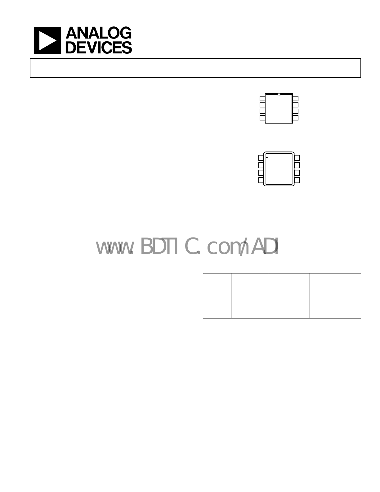
PIN CONFIGURATIONS
NC
1
ADR293
V
2
IN
TOP VIEW
NC
3
(Not to Scale)
4
GND
NC = NO CONNECT
Figure 1. 8-Lead Narrow Body SOIC (R-8)
1
NC
2
V
NC
GND
ADR293
IN
TOP VIEW
3
(Not to Scale)
4
NC = NO CONNECT
Figure 2. 8-Lead TSSOP (RU-8)
15 ppm/°C, and 25 ppm/°C maximum. Line regulation and load
regulation are typically 30 ppm/V and 30 ppm/mA, respectively,
maintaining the reference’s overall high performance.
The ADR293 is specified over the extended industrial
emperature range of –40°C to +125°C. This device is available
t
in the 8-lead SOIC and 8-lead TSSOP packages.
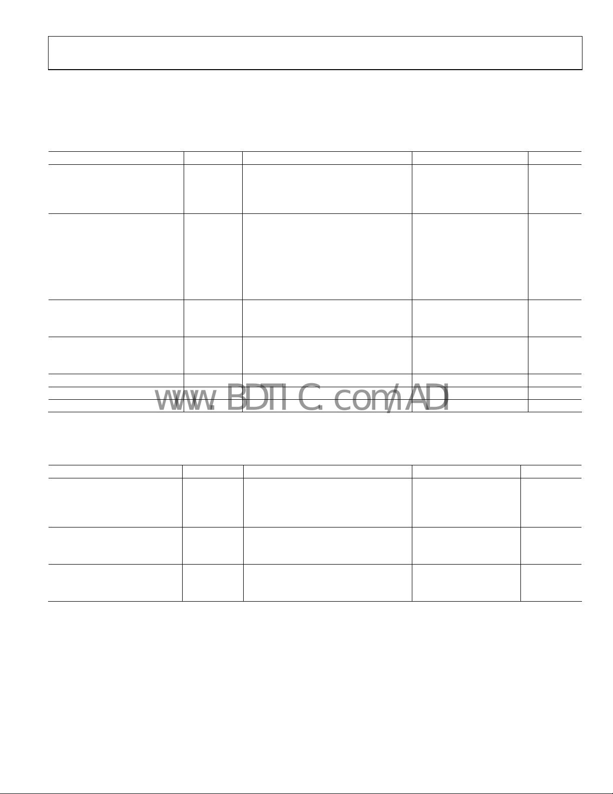
Table 1. ADR29x Products
Device
Output
V
oltage (V)
Initial
Accuracy (%)
ADR291 2.500 0.08, 0.12, 0.24 8, 15, 25
ADR292 4.096 0.07, 0.10, 0.15 8, 15, 25
ADR293 5.000 0.06, 0.12, 0.20 8, 15, 25
NC
8
NC
7
V
6
OUT
5
NC
8
NC
7
NC
6
V
OUT
5
NC
00164-001
00164-002
Temperature
C
oefficient
(ppm/°C max)
Rev. B
Information furnished by Analog Devices is believed to be accurate and reliable. However, no
responsibility is assumed by Anal og Devices for its use, nor for any infringements of patents or ot her
rights of third parties that may result from its use. Specifications subject to change without notice. No
license is granted by implication or otherwise under any patent or patent rights of Analog Devices.
Trademarks and registered trademarks are the property of their respective owners.
One Technology Way, P.O. Box 9106, Norwood, MA 02062-9106, U.S.A.
Tel: 781.329.4700 www.analog.com
Fax: 781.461.3113 ©2007 Analog Devices, Inc. All rights reserved.

ADR293
www.BDTIC.com/ADI
TABLE OF CONTENTS
Features.............................................................................................. 1
Applications....................................................................................... 1
Pin Configurations ........................................................................... 1
General Description ......................................................................... 1
Revision History ............................................................................... 2
Specifications..................................................................................... 3
Electrical Specificiations.............................................................. 3
Absolute Maximum Ratings............................................................ 5
Thermal Resistance ...................................................................... 5
ESD Caution.................................................................................. 5
Typical Performance Characteristics ............................................. 6
Terminology ...................................................................................... 9
Theory of Operation ...................................................................... 10
REVISION HISTORY
6/07—Rev. A to Rev. B
Updated Format..................................................................Universal
Changes to Table 1............................................................................ 1
Updated Outline Dimensions....................................................... 13
Changes to Ordering Guide.......................................................... 13
3/01—Rev. 0 to Rev. A
Device Power Dissipation Considerations.............................. 10
Basic Voltage Reference Connections ..................................... 10
Noise Performance..................................................................... 10
Turn-On Time ............................................................................ 10
Applications..................................................................................... 11
A Negative Precision Reference Without Precision
Resistors....................................................................................... 11
A Precision Current Source...................................................... 11
Kelvin Connections.................................................................... 11
Voltage Regulator for Portable Equipment............................. 12
Outline Dimensions....................................................................... 13
Ordering Guide .......................................................................... 14
Rev. B | Page 2 of 16
ADR293
www.BDTIC.com/ADI
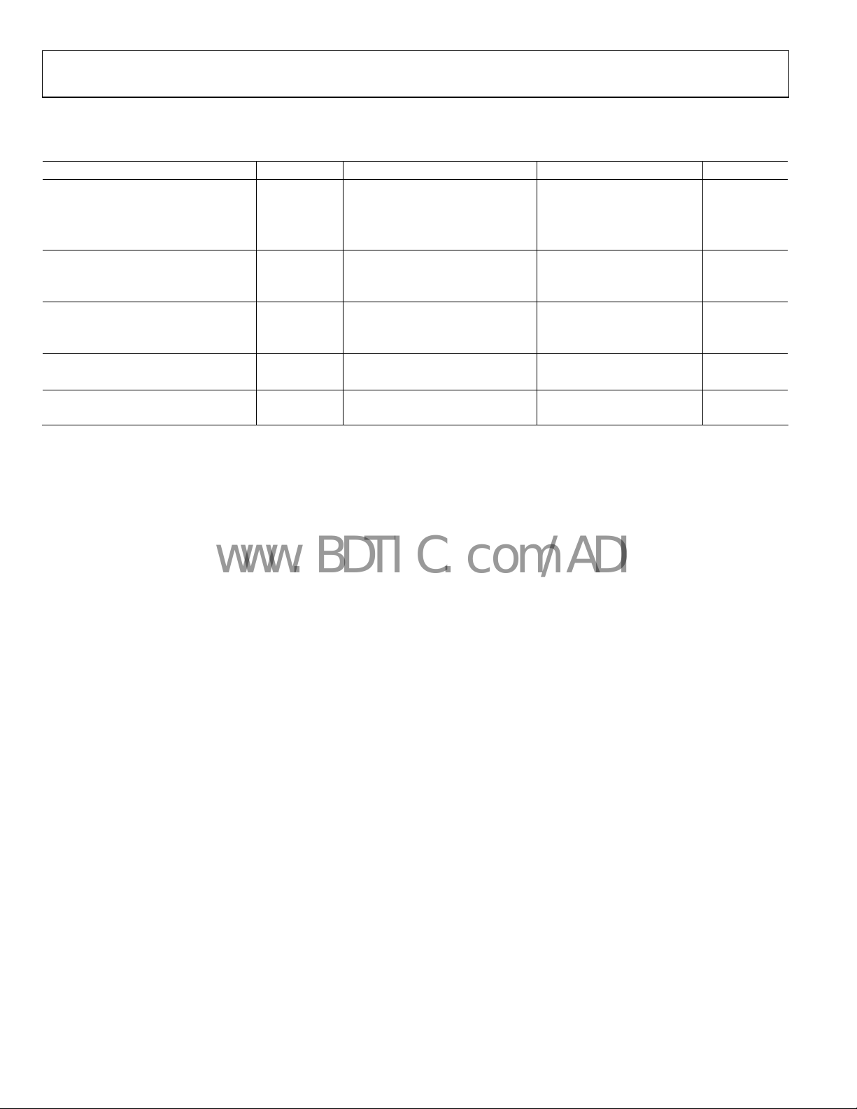
SPECIFICATIONS
ELECTRICAL SPECIFICIATIONS
VS = 6.0 V, TA = 25°C, unless otherwise noted.
Table 2.
Parameter Symbol Conditions Min Typ Max Unit
OUTPUT VOLTAGE V
E Grade 4.997 5.000 5.003 V
F Grade 4.994 5.000 5.006 V
G Grade 4.990 5.000 5.010 V
INITIAL ACCURACY I
E Grade –3 +3 mV
0.06 %
F Grade –6 +6 mV
0.12 %
G Grade –10 +10 mV
0.20 %
LINE REGULATION ΔV
E, F Grades 30 100 ppm/V
G Grade 40 150 ppm/V
LOAD REGULATION ΔV
E, F Grades 30 100 ppm/mA
G Grade 40 150 ppm/mA
LONG-TERM STABILITY ΔV
NOISE VOLTAGE eN 0.1 Hz to 10 Hz 15 μV p-p
WIDEBAND NOISE DENSITY eN at 1 kHz 640 nV/√Hz
V
= 6.0 V, TA = −25°C to +85°C, unless otherwise noted.
S
I
OUT
/ΔVIN 6.0 V to 15 V, I
OUT
/ΔI
OUT
LOAD
After 1000 hours of operation @ 125°C 50 ppm
OUT
= 0 mA
OUT
= 0 mA
OUT
= 0 mA
OUT
VS = 6.0 V, 0 mA to 5 mA
Table 3.
Parameter Symbol Conditions Min Typ Max Unit
TEMPERATURE COEFFICIENT TCV
I
OUT
OUT
= 0 mA
E Grade 3 8 ppm/°C
F Grade 5 15 ppm/°C
G Grade 10 25 ppm/°C
LINE REGULATION ΔV
/ΔVIN 6.0 V to 15 V, I
OUT
= 0 mA
OUT
E, F Grades 35 150 ppm/V
G Grade 50 200 ppm/V
LOAD REGULATION ΔV
OUT
/ΔI
VS = 6.0 V, 0 mA to 5 mA
LOAD
E, F Grades 20 150 ppm/mA
G Grade 30 200 ppm/mA
Rev. B | Page 3 of 16
ADR293
www.BDTIC.com/ADI
VS = 6.0 V, TA = −40°C to +125°C, unless otherwise noted.
Table 4.
Parameter Symbol Conditions Min Typ Max Unit
TEMPERATURE COEFFICIENT TCV
E Grade 3 10 ppm/°C
F Grade 5 20 ppm/°C
G Grade 10 30 ppm/°C
LINE REGULATION ΔV
E, F Grades 40 200 ppm/V
G Grade 70 250 ppm/V
LOAD REGULATION ΔV
E, F Grades 20 200 ppm/mA
G Grade 30 300 ppm/mA
SUPPLY CURRENT IS @ 25°C 11 15 μA
15 20 μA
THERMAL HYSTERESIS V
8-lead TSSOP 157 ppm
I
OUT
/ΔVIN 6.0 V to 15 V, I
OUT
/ΔI
OUT
LOAD
8-lead SOIC_N 72 ppm
OUT-HYS
= 0 mA
OUT
= 0 mA
OUT
VS = 6.0 V, 0 mA to 5 mA
Rev. B | Page 4 of 16
ADR293
www.BDTIC.com/ADI
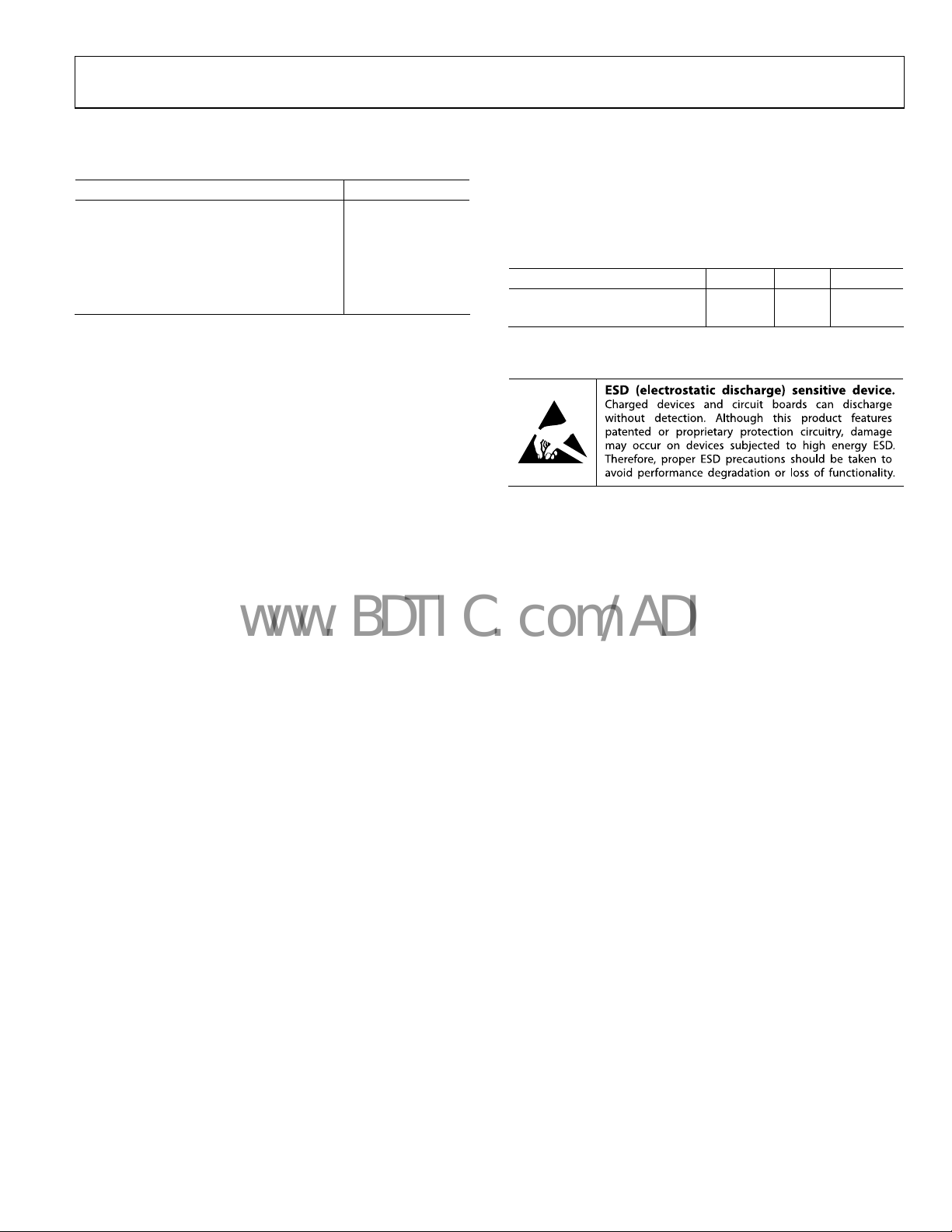
ABSOLUTE MAXIMUM RATINGS
Table 5.
Parameter Rating
Supply Voltage 18 V
Output Short-Circuit Duration to GND Indefinite
Storage Temperature Range −65°C to +150°C
Operating Temperature Range −40°C to +125°C
Junction Temperature Range −65°C to +150°C
Lead Temperature (Soldering, 60 sec) 300°C
Stresses above those listed under Absolute Maximum Ratings
y cause permanent damage to the device. This is a stress
ma
rating only; functional operation of the device at these or any
other conditions above those indicated in the operational
section of this specification is not implied. Exposure to absolute
maximum rating conditions for extended periods may affect
device reliability.
THERMAL RESISTANCE
θJA is specified for worst-case conditions; that is, θJA is specified
for device in socket testing. In practice, θ
device soldered in circuit board.
Table 6. Thermal Resistance
Package Type θJA θ
8-Lead SOIC_N (R-8) 158 43 °C/W
8-Lead TSSOP (RU-8) 240 43 °C/W
is specified for a
JA
Unit
JC
ESD CAUTION
Rev. B | Page 5 of 16

ADR293
T
A
A
A
www.BDTIC.com/ADI
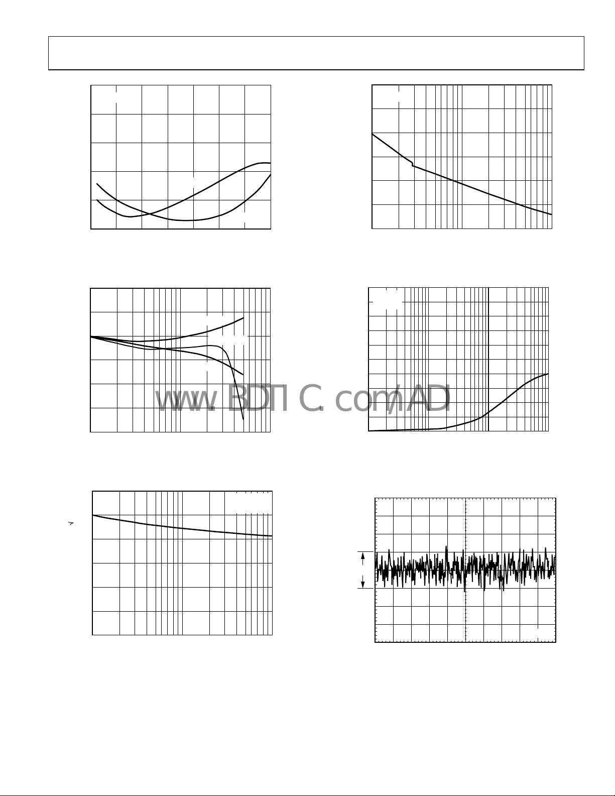
TYPICAL PERFORMANCE CHARACTERISTICS
AGE (V)
OUTPUT VOL
5.006
5.004
5.002
5.000
4.998
4.996
VS = 6V
3 TYPICAL PARTS
TION (ppm/V)
LINE REGUL
100
80
60
40
20
VS = 6V TO 15V
4.994
–50 –25 0 25 50 75 100 125
16
14
12
10
8
6
SUPPLY CURRENT (µA)
4
2
0
0 2 4 6 8 10 12 14 16
TEMPERATURE (°C)
Figure 3. V
INPUT VOLTAGE (V)
vs. Temperature
OUT
TA = +125°C
TA = +25°C
TA = –40°C
Figure 4. Supply Current vs. Input Voltage
16
VS = 6V
14
12
10
SUPPLY CURRENT (µA)
8
0
00164-003
–50 –25 0 25 50 75 100 125
TEMPERATURE (°C)
00164-006
Figure 6. Line Regulation vs. Temperature
100
I
VS = 6V TO 9V
80
60
TION (ppm/V)
40
LINE REGUL
20
0
00164-004
–50 –25 0 25 50 75 100 125
TEMPERATURE (°C)
OUT
= 0mA
00164-007
Figure 7. Line Regulation vs. Temperature
0.7
0.6
0.5
0.4
L VOLTAGE (V)
0.3
0.2
DIFFERENTI
0.1
TA = +125°C
TA = +25°C
TA = –40°C
6
–50 –25 0 25 50 75 100 125
TEMPERATURE (°C)
00164-005
Figure 5. Supply Current vs. Temperature
Rev. B | Page 6 of 16
0
0 0.5 1.0 1.5 2.0 2.5 3.0 3.5 4.0 4.5 5.0
Figure 8. Minimum Input/Output Volt
LOAD CURRENT (mA)
age Differential vs. Load Current
00164-008
ADR293
A
A
www.BDTIC.com/ADI
200
VS = 6V
160
120
TION (ppm/mA)
80
I
= 5mA
OUT
LOAD REGUL
40
I
= 1mA
OUT
0
–50 –25 0 25 50 75 100 125
TEMPERATURE (°C)
Figure 9. Load Regulation vs. Temperature
00164-009
120
VS = 6V
100
80
60
40
RIPPLE REJECT ION (d B)
20
0
10 100 1k
FREQUENCY (Hz)
Figure 12. Ripple Rejection vs. Frequency
00164-012
2
1
L (mV)
0
–1
FROM NOMIN
–2
OUT
ΔV
–3
–4
10 100 1k
Figure 10. ΔV
1200
1000
800
600
SOURCING LO AD CURRENT (mA)
from Nominal vs. Load Current
OUT
TA = +25°C
TA = –40°C
TA = +125°C
VIN = 15V
T
A
= 25°C
50
VS = 6V
= 0mA
I
L
40
30
20
OUTPUT IMPEDANCE (Ω)
10
0
10 100 1k 10k
00164-010
Figure 13. Output Imped
10µV p-p
FREQUENCY ( Hz)
ance vs. Frequency
00164-013
400
200
VOLTAGE NOISE DENSITY (nV/ Hz)
0
10 100 1k
FREQUENCY ( Hz)
00164-011
Figure 11. Voltage Noise Density
Rev. B | Page 7 of 16
Figure 14. 0.1 Hz to 10 Hz Noise
1s/DIV
00164-014

ADR293
www.BDTIC.com/ADI
IL = 5mA
5V/DIV
2V/DIV
II = 5mA
C
= 1nF
L
IL = 5mA
IL = 5mA
Figure 15. Turn-On Time
5V/DIV
2V/DIV
Figure 16. Turn-Off Time
Figure 17. Load Transient
50µs/DIV
50µs/DIV
1ms/DIV
0164-015
1ms/DIV
00164-018
Figure 18. Load Transient
II = 5mA
C
= 100nF
L
00164-016
1ms/DIV
00164-019
Figure 19. Load Transient
18
16
14
12
10
8
6
4
FREQUENCY I N NUMBER OF UNITS
2
0
00164-017
–200 –160 –120 –80 –40 0 40 80 120 160 200 240
V
DEVIATION (ppm)
OUT
Figure 20. Typical Hysteresis f
TEMPERATURE
+25°C → –40°C →
+85°C → +25°C
or ADR29x Product
00164-020
Rev. B | Page 8 of 16

ADR293
www.BDTIC.com/ADI
TERMINOLOGY
Line Regulation
The change in output voltage due to a specified change in input
v
oltage. It includes the effects of self-heating. Line regulation is
expressed in percent per volt, parts per million per volt, or
microvolts per volt change in input voltage.
Load Regulation
The change in output voltage due to a specified change in load
urrent. It includes the effects of self-heating. Load regulation is
c
expressed in microvolts per milliampere, parts per million per
milliampere, or ohms of dc output resistance.
Long-Term Stability
Typical shift of output voltage of 25°C on a sample of parts
s
ubjected to high temperature operating life test of 1000 hours
at 125°C.
( )
0
OUTOUT
[]
V
OUT
OUT
=Δ
()
tVtVV −=Δ
OUT
()
−
0
()
OUT
tV
1
0
OUT
()
tVtV
1
6
10ppm ×
where:
V
V
OUT (t0
(t1) = V
OUT
) = V
at 25°C at time 0.
OUT
at 25°C after 1000 hours operation at 125°C.
OUT
NC = No Connect
There are in fact connections at NC pins, which are reserved for
manufacturing purposes. Users should not connect anything at
NC pins.
Temperature Coefficient
The change of output voltage over the operating temperature
change and normalized by the output voltage at 25°C, expressed
in ppm/°C.
[]
VTC
OUT
=°
2
OUT
()
OUT
−
TVΤV
1
OUT
()
−×°
TTC25V
6
10Cppm/ ×
12
() ( )
where:
V
(25°C) = V
OUT
V
(T1) = V
OUT
V
(T2) = V
OUT
at 25°C.
OUT
at Temperature 1.
OUT
at Temperature 2.
OUT
Thermal Hysteresis
Thermal hysteresis is defined as the change of output voltage
after the device is cycled through temperatures from +25°C to
–40°C to +85°C and back to +25°C. This is a typical value from
a sample of parts put through such a cycle.
( )
[]
V
−
HYSOUT
=
VC25VV
−°=
()
TCOUTOUTHYSOUT
−−
−°
VC25V
()
°
OUT
C25V
−
TCOUTOUT
6
10ppm ×
where:
V
V
OUT
OUT-TC
(25°C) = V
= V
OUT
at 25°C.
OUT
(25°C) after temperature cycle at +25°C to –40°C
to +85°C and back to +25°C.
Rev. B | Page 9 of 16

ADR293
V
−
www.BDTIC.com/ADI
THEORY OF OPERATION
The ADR293 uses a new reference generation technique known
as XFET, which yields a reference with low noise, low supply
current, and very low thermal hysteresis.
The core of the XFET reference consists of two junction field
fect transistors, one of which has an extra channel implant to
ef
raise its pinch-off voltage. By running the two JFETs at the same
drain current, the difference in pinch-off voltage can be amplified
and used to form a highly stable voltage reference. The intrinsic
reference voltage is around 0.5 V with a negative temperature
coefficient of about –120 ppm/K. This slope is essentially locked
to the dielectric constant of silicon and can be closely compensated by adding a correction term generated in the same fashion
as the proportional-to-temperature (PTAT) term used to
compensate band gap references. The big advantage over a band
gap reference is that the intrinsic temperature coefficient is
some 30 times lower (therefore, less correction is needed) and
this results in much lower noise, because most of the noise of a
band gap reference comes from the temperature compensation
circuitry.
The simplified schematic in Figure 21 shows the basic topology
f the ADR293. The temperature correction term is provided by
o
a current source with value designed to be proportional to
absolute temperature. The general equation is
++
OUT
⎛
Δ=
VV
⎜
P
⎝
R1
R3R2R1
⎞
()
+
⎟
PTAT
⎠
()
R3I
where:
ΔV
is the difference in pinch-off voltage between the two FETs.
P
I
is the positive temperature coefficient correction current.
PTAT
The process used for the XFET reference also features vertical
NPN an
d PNP transistors, the latter of which are used as output
devices to provide a very low dropout voltage.
IN
I
1I1
1
1
EXTRA CHANNEL IMP LANT
R1 + R2 + R3
=×ΔVP + I
V
OUT
R1
Figure 21. Simplifi
ΔV
P
R1
R2
R3
× R3
PTAT
ed Schematic
I
PTAT
GND
V
OUT
00164-021
DEVICE POWER DISSIPATION CONSIDERATIONS
The ADR293 is guaranteed to deliver load currents to 5 mA
with an input voltage that ranges from 5.5 V to 15 V. When
this device is used in applications with large input voltages,
care should be exercised to avoid exceeding the published
specifications for maximum power dissipation or junction
temperature that could result in premature device failure.
The following formula should be used to calculate a device’s
maximum junction temperature or dissipation:
TT
J
A
P
=
D
θ
JA
where:
T
and TA are the junction temperature and ambient
J
temperature, respectively.
P
is the device power dissipation.
D
θ
is the device package thermal resistance.
JA
BASIC VOLTAGE REFERENCE CONNECTIONS
References, in general, require a bypass capacitor connected
from the V
pin to the GND pin. The circuit in Figure 22
OUT
illustrates the basic configuration for the ADR293. Note that the
decoupling capacitors are not required for circuit stability.
1
NC
ADR293
2
3
+
10µF
Figure 22. Basic Voltage Reference Configuration
0.1µF
NC
4
NC = NO CONNECT
8
NC
7
NC
V
OUT
6
5
NC
0.1µF
00164-022
NOISE PERFORMANCE
The noise generated by the ADR293 is typically less than
15 μV p-p over the 0.1 Hz to 10 Hz band. The noise measurement is made with a band-pass filter made of a 2-pole high-pass
filter with a corner frequency at 0.1 Hz and a 2-pole low-pass
filter with a corner frequency at 10 Hz.
TURN-ON TIME
Upon application of power (cold start), the time required for
the output voltage to reach its final value within a specified
error band is defined as the turn-on settling time. Two
components normally associated with this are the time for the
active circuits to settle and the time for the thermal gradients on
the chip to stabilize. Figure 15 shows the typical turn-on time
or the ADR293.
f
Rev. B | Page 10 of 16

ADR293
V
V
www.BDTIC.com/ADI
APPLICATIONS
R1
P1
R
LW
, which sets
SET
R
SET
00164-024
+V
OUT
SENSE
+V
OUT
FORCE
R
L
0164-025
A NEGATIVE PRECISION REFERENCE WITHOUT PRECISION RESISTORS
In many current-output CMOS DAC applications where the
output signal voltage must be of the same polarity as the
reference voltage, it is often required to reconfigure a currentswitching DAC into a voltage-switching DAC by using a 1.25 V
reference, an op amp, and a pair of resistors. Using a currentswitching DAC directly requires the need for an additional
operational amplifier at the output to reinvert the signal.
Therefore, a negative voltage reference is desirable from the
point that an additional operational amplifier is not required for
either reinversion (current-switching mode) or amplification
(voltage-switching mode) of the DAC output voltage. In
general, any positive voltage reference can be converted into a
negative voltage reference by using an operational amplifier and
a pair of matched resistors in an inverting configuration. The
disadvantage to that approach is that the largest single source of
error in the circuit is the relative matching of the resistors used.
The circuit illustrated in Figure 23 avoids the need for tightly
m
atched resistors with the use of an active integrator circuit. In
this circuit, the output of the voltage reference provides the
input drive for the integrator. To maintain circuit equilibrium,
the integrator adjusts its output to establish the proper
relationship between the reference’s V
and GND. One caveat
OUT
with this approach should be mentioned. Although rail-to-rail
output amplifiers work best in the application, these operational
amplifiers require a finite amount (mV) of headroom when
required to provide any load current. The choice for the circuit’s
negative supply should take this issue into account.
IN
2
ADR293
V
6
OUT
GND
100kΩ
4
Figure 23. A Negative Precision Voltage Reference Uses No
1µF
1kΩ
+5V
1µF
A1 = 1/2 OP291, 1/2 OP295
100Ω
A1
–5V
–V
REF
00164-023
Precision Resistors
A PRECISION CURRENT SOURCE
Many times in low power applications, the need arises for a
precision current source that can operate on low supply
voltages. As shown in Figure 24, the ADR293 is configured as a
recision current source. The circuit configuration illustrated is
p
a floating current source with a grounded load. The output
voltage of the reference is bootstrapped across R
the output current into the load. With this configuration, circuit
precision is maintained for load currents in the range from the
reference’s supply current, typically 15 μA to approximately 5 mA.
IN
2
ADR293
V
6
OUT
GND
4
1µF
ADJUST
I
SY
I
OUT
R
L
Figure 24. A Precision Current Source
KELVIN CONNECTIONS
In many portable instrumentation applications where PC board
cost and area go hand-in-hand, circuit interconnects are very
often of dimensionally minimum width. These narrow lines
can cause large voltage drops if the voltage reference is required
to provide load currents to various functions. In fact, a circuit’s
interconnects can exhibit a typical line resistance of 0.45 mΩ/
square (1 oz. Cu, for example). Force and sense connections,
also referred to as Kelvin connections, offer a convenient
method of eliminating the effects of voltage drops in circuit
wires. Load currents flowing through wiring resistance produce
an error (V
connection in Figure 25 overcomes the problem by including
he wiring resistance within the forcing loop of the op amp.
t
Because the op amp senses the load voltage, op amp loop
control forces the output to compensate for the wiring error and
to produce the correct voltage at the load.
= R × IL) at the load. However, the Kelvin
ERROR
V
IN
2
R
LW
V
IN
ADR293
A1
100kΩ
GND
4
V
6
OUT
1µF
Figure 25. Advantage of Kelvin Connection
Rev. B | Page 11 of 16

ADR293
www.BDTIC.com/ADI
VOLTAGE REGULATOR FOR PORTABLE EQUIPMENT
The ADR293 is ideal for providing a stable, low cost, and low
power reference voltage in portable equipment power supplies.
Figure 26 shows how the ADR293 can be used in a voltage
egulator that not only has low output noise (as compared to
r
switch mode design) and low power, but also a very fast
recovery after current surges. Some precautions should be taken
in the selection of the output capacitors. Too high an ESR
(effective series resistance) could endanger the stability of the
circuit. A solid tantalum capacitor, 16 V or higher, and an
aluminum electrolytic capacitor, 10 V or higher, are recommended for C1 and C2, respectively. In addition, the path from
the ground side of C1 and C2 to the ground side of R1 should
be kept as short as possible.
CHARGER
INPUT
LEAD-ACID
BATTERY
0.1µF
2
V
IN
R3
510kΩ
ADR293
V
GND
4
OUT
402kΩ
6 2
R1
1%
6V
+
7
6
OP20
3
4
R2
402kΩ
1%
68µF
TANT
IRF9530
C1
Figure 26. Voltage Regulator for Portable Equipment
5V, 100mA
C2
++
1000µF
ELECT
00164-026
Rev. B | Page 12 of 16

ADR293
Y
www.BDTIC.com/ADI
OUTLINE DIMENSIONS
5.00 (0.1968)
4.80 (0.1890)
4.00 (0.1574)
3.80 (0.1497)
0.25 (0.0098)
0.10 (0.0040)
COPLANARITY
0.10
CONTROLL ING DIMENSI ONS ARE IN MILLIMETERS; INCH DI MENSIONS
(IN PARENTHESES) ARE ROUNDED-OFF MILLIMETER EQUIVALENTS FOR
REFERENCE ONLY AND ARE NOT APPROPRI ATE FOR USE IN DES IGN.
85
1
1.27 (0.0500)
SEATING
PLANE
COMPLIANT TO JEDEC STANDARDS MS-012-A A
BSC
6.20 (0.2441)
5.80 (0.2284)
4
1.75 (0.0688)
1.35 (0.0532)
0.51 (0.0201)
0.31 (0.0122)
8°
0°
0.25 (0.0098)
0.17 (0.0067)
0.50 (0.0196)
0.25 (0.0099)
1.27 (0.0500)
0.40 (0.0157)
45°
012407-A
Figure 27. 8-Lead Standard Small Outline Package [SOIC_N]
Nar
row Body
(R-8)
Dimensions shown in millimeters and (inches)
3.10
3.00
2.90
8
5
4.50
6.40 BSC
4.40
4.30
41
PIN 1
0.15
0.05
COPLANARIT
Figure 28. 8-Lead Thin Shrink Small Outline Package [TSSOP]
0.65 BSC
1.20
MAX
0.30
SEATING
0.19
0.10
COMPLIANT TO JEDEC STANDARDS MO-153-AA
PLANE
0.20
0.09
8°
0°
(RU-8)
Dim
ensions shown in millimeters
0.75
0.60
0.45
Rev. B | Page 13 of 16
ADR293
www.BDTIC.com/ADI
ORDERING GUIDE
Temperature
Output
Model
ADR293ER 5.00 0.06 8 −40°C to +125°C 8-Lead SOIC_N R-8 98
ADR293ER-REEL 5.00 0.06 8 −40°C to +125°C 8-Lead SOIC_N R-8 2,500
ADR293ERZ
ADR293ERZ-REEL
ADR293FR 5.00 0.12 15 −40°C to +125°C 8-Lead SOIC_N R-8 98
ADR293FRZ
ADR293GR 5.00 0.20 25 −40°C to +125°C 8-Lead SOIC_N R-8 98
ADR293GR-REEL7 5.00 0.20 25 −40°C to +125°C 8-Lead SOIC_N R-8 1,000
ADR293GRZ
ADR293GRZ-REEL715.00 0.20 25 −40°C to +125°C 8-Lead SOIC_N R-8 1,000
ADR293GRU 5.00 0.20 25 −40°C to +125°C 8-Lead TSSOP RU-8 96
ADR293GRU-REEL 5.00 0.20 25 −40°C to +125°C 8-Lead TSSOP RU-8 2,500
ADR293GRU-REEL7 5.00 0.20 25 −40°C to +125°C 8-Lead TSSOP RU-8 1,000
ADR293GRUZ
ADR293GRUZ-REEL15.00 0.20 25 −40°C to +125°C 8-Lead TSSOP RU-8 2,500
ADR293GRUZ-REEL715.00 0.20 25 −40°C to +125°C 8-Lead TSSOP RU-8 1,000
1
Z = RoHS Compliant Part.
1
1
1
1
V
oltage (V)
5.00 0.06 8 −40°C to +125°C 8-Lead SOIC_N R-8 98
1
5.00 0.06 8 −40°C to +125°C 8-Lead SOIC_N R-8 2,500
5.00 0.12 15 −40°C to +125°C 8-Lead SOIC_N R-8 98
5.00 0.20 25 −40°C to +125°C 8-Lead SOIC_N R-8 98
5.00 0.20 25 −40°C to +125°C 8-Lead TSSOP RU-8 96
Initial
Accuracy (%)
C
oefficient
(ppm/°C max)
Temperature
nge
Ra
Package
Description
Package
Option
Ordering
Quantity
Rev. B | Page 14 of 16

ADR293
www.BDTIC.com/ADI
NOTES
Rev. B | Page 15 of 16

ADR293
www.BDTIC.com/ADI
NOTES
©2007 Analog Devices, Inc. All rights reserved. Trademarks and
registered trademarks are the property of their respective owners.
C00164-0-6/07(B)
Rev. B | Page 16 of 16
 Loading...