Analog Devices ADR280 b Datasheet

1.2 V Ultralow Power
V
OUT
V
IN
1
2
3
ADR280
GND
V
IN
V
OUT
1
2
3
ADR280
GND
TEMPERATURE (C)
15
–15
–40 100–20
LINE REGULATION (ppm/V)
0 20 40 60 80
–10
–5
0
5
10
3V TO 5V
High PSRR Voltage Reference
ADR280
FEATURES
1.2 V Precision Output
Excellent Line Regulation, 2 ppm/V Typical
High Power Supply Ripple Rejection, –80 dB at 220 Hz
Ultralow Power, Supply Current 16 A Maximum
Temperature Coefcient, 40 ppm/oC Maximum
Low Noise, 12.5 nV/÷Hz Typical
Operating Supply Range, 2.4 V to 5.5 V
Compact 3-Lead SOT-23 and SC70 Packages
APPLICATIONS
GSM, GPRS, 3G Mobile Stations
Portable Battery-Operated Electronics
Low Voltage Converter References
Wireless Devices
GENERAL DESCRIPTION
The ADR280 is a 1.2 V band gap core reference with excellent
line regulation and power supply rejection designed specically
for applications experiencing heavy dynamic supply variations,
such as data converter references in GSM, GPRS, and 3G
mobile station applications. Devices such as the AD6535, that has
an analog baseband IC with on-board baseband and audio codecs,
voltage regulators, and battery charger rely on the ADR280’s
ability to reject input battery voltage variations during RF power
amplier activity.
In addition to mobile stations, the ADR280 is suitable for a variety of general-purpose applications. Most band gap references
include internal gain for specic outputs, which simplies the
user’s design, but compromises on the cost, form factor, and
exibility. The ADR280, on the other hand, optimizes the band
gap core voltage and allows users to tailor the voltage, current, or
transient response by simply adding their preferred op amps.
The ADR280 operates on a wide supply voltage range from 2.4 V
to 5.5 V. It is available in compact 3-lead SOT-23 and
SC70
packages. The device is specied over the extended indus-
trial temperature range of –40°C to +85°C.
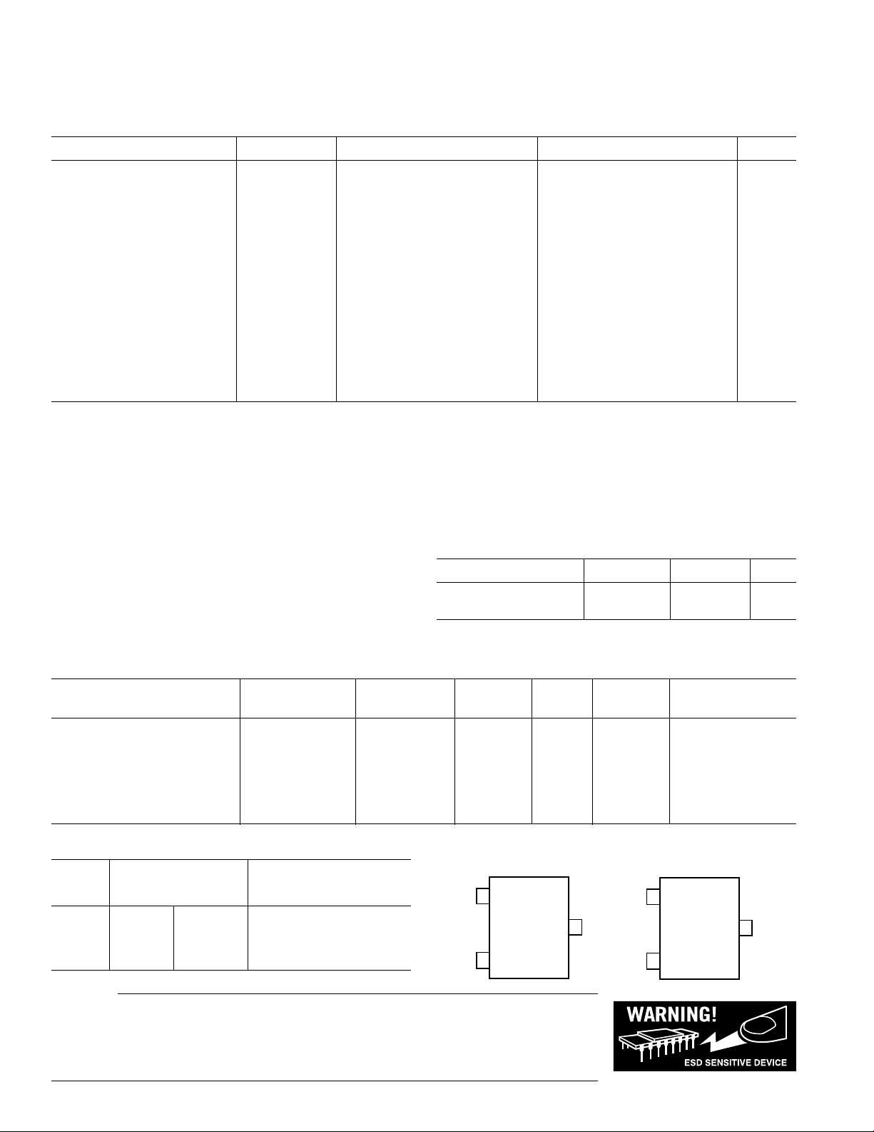
PIN CONFIGURATIONS
3-Lead SOT-23
(RT Sufx)
3-Lead SC70
(KS Sufx)
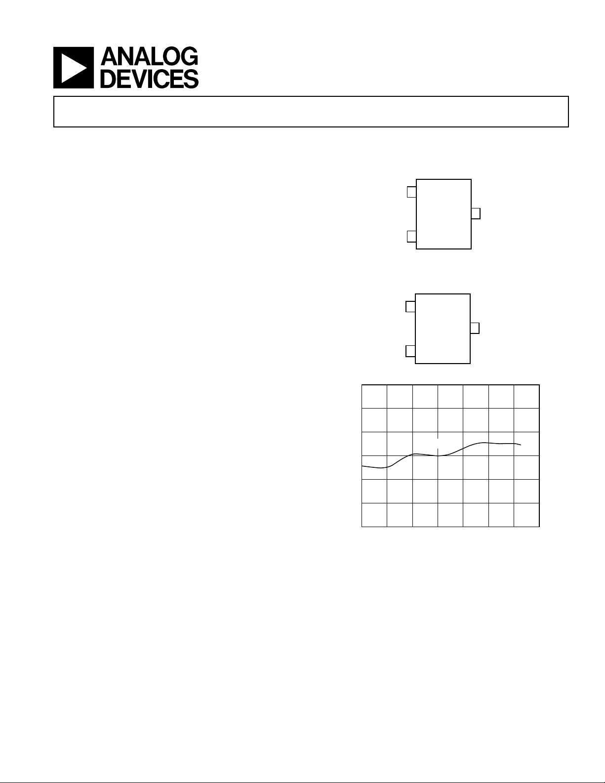
Figure 1. Line Regulation vs. Temperature
REV. B
Information furnished by Analog Devices is believed to be accurate and
reliable. However, no responsibility is assumed by Analog Devices for its
use, nor for any infringements of patents or other rights of third parties
that may result from its use. No license is granted by implication or otherwise under any patent or patent rights of Analog Devices. Trademarks
and registered trademarks are the property of their respective owners.
One Technology Way, P.O. Box 9106, Norwood, MA 02062-9106, U.S.A.
Tel: 781/329-4700 www.analog.com
Fax: 781/326-8703 © 2004 Analog Devices, Inc. All rights reserved.

ADR280–SPECIFICATIONS
V
OUT
V
IN
1
2
3
ADR280
GND
V
IN
V
OUT
1
2
3
ADR280
GND
ELECTRICAL CHARACTERISTICS
(VIN = 2.55 V to 5.5 V, TA = 25°C, unless otherwise noted.)
Parameter Symbol Conditions Min Typ1 Max Unit
Output Voltage2 V
1.195 1.200 1.205 V
OUT
Temperature Coefcient TCVo 0°C < TA < 50°C 5 20 ppm/oC
–40°C < TA < +85°C 10 40 ppm/oC
Line Regulation V
/VIN 2.55 V < VIN < 5.5 V, No Load 2 12 ppm/V
OUT
Supply Current IIN 2.4 V < VIN < 5.5 V, No Load 10 16 µA
Ground Current I
V– Grounded, I
GND
= 10 µA 12 20 µA
LOAD
Input Voltage Range VIN 2.4 5.5 V
Operating Temperature Range T
Nominal Load Capacitance C
A
1 µF
OUT
–40 +85 °C
Output Noise Voltage VN f = 10 Hz to 10 kHz 12.5 µVrms
Output Noise Density eN f = 400 kHz 12.5 nV/÷Hz
Power Supply Ripple Rejection3 PSRR I
= 10 µA –80 dB
LOAD
Start-Up Time tON 2 ms
NOTES
1
Typical values represent average readings taken at room temperature.
2
Conditions: 2.4 V < VIN < 5.5 V, 0 µA < I
3
Power supply ripple rejection measurement applies to a changing input voltage (VIN) waveform with a nominal 3.6 V baseline that drops to a 3 V value for
380 µs at a 4.6 ms repetition rate.
Specications subject to change without notice.
ABSOLUTE MAXIMUM RATINGS
Supply Voltage . . . . . . . . . . . . . . . . . . . . . . . . . . . . . . . . . . . 6 V
Storage Temperature Range . . . . . . . . . . . . . . –65°C to +150°C
Operating Temperature Range . . . . . . . . . . . . . –40°C to +85°C
Junction Temperature Range . . . . . . . . . . . . . . –65°C to +150°C
Lead Temperature Range (Soldering, 60 Sec) . . . . . . . . . .300°C
NOTES
1
Stresses above those listed under Absolute Maximum Ratings may cause permanent
damage to the device. This is a stress rating only and functional operation of the
device at these or any other conditions above those listed in the operational sections
< 10 µA, –40°C < TA < +85°C.
OUT
1, 2
of this specication is not implied. Exposure to absolute maximum rating conditions
for extended periods may affect device reliability.
2
Absolute Maximum Ratings apply at 25°C, unless otherwise noted.
THERMAL RESISTANCE
Package Type JA*
JC
Unit
SOT-23 230 146 °C/W
SC70 376 102 °C/W
* JA is specied for the worst-case conditions, i.e., JA is specied for device sol-
dered in circuit board for surface-mount packages.
ORDERING GUIDE
Temperature Package Package Top Output Number of
Model Range Description Option Mark Voltage (V) Parts per Reel
ADR280ART-R2 –40°C to +85°C SOT-23 RT-3 RBA 1.200 250
ADR280ART-REEL7 –40°C to +85°C SOT-23 RT-3 RBA 1.200 3,000
ADR280ART-REEL –40°C to +85°C SOT-23 RT-3 RBA 1.200 10,000
ADR280ARTZ-REEL7* –40°C to +85°C SOT-23 RT-3 RBA 1.200 3,000
ADR280AKS-R2 –40°C to +85°C SC70 KS-3 RBA 1.200 250
ADR280AKS-REEL7 –40°C to +85°C SC70 KS-3 RBA 1.200 3,000
ADR280AKS-REEL –40°C to +85°C SC70 KS-3 RBA 1.200 10,000
*Z = Pb-free part.
PIN FUNCTION DESCRIPTIONS
Mnemonic
PIN CONFIGURATIONS
SOT-23
SC70
Pin No. SOT-23 SC70 Description
1 V+ V
2 V
OUT
High Supply Voltage Input
OUT
V+ Output Voltage
3 V– V– Low Supply Voltage Input
CAUTION
ESD (electrostatic discharge) sensitive device. Electrostatic charges as high as 4000 V readily accumulate
on the human body and test equipment and can discharge without detection. Although the ADR280
features proprietary ESD protection circuitry, permanent damage may occur on devices subjected to high
energy electrostatic discharges. Therefore, proper ESD precautions are recommended to avoid performance
degradation or loss of functionality.
–2–
REV. B REV. B

Typical Performance Characteristics–ADR280
TEMPERATURE (C)
1.20225
–40 100–20
V
OUT
(V)
0 20 40 60 80
NO LOAD
1.20200
1.20175
1.20150
1.20125
1.20100
1.20075
1.20050
1.20025
1.20000
TEMPERATURE (C)
–40 100–20
I
IN
(A)
0 20 40 60 80
VIN = 5V
15
14
13
12
11
10
9
VIN = 3V
TEMPERATURE (C)
15
–15
–40 100–20
LINE REGULATION (ppm/V)
0 20 40 60 80
–10
–5
0
5
10
3V TO 5V
Ch1 50.0V M 1.00 s
1
–100
–80
–60
–40
NOISE POWER DENSITY (dBm)
10.07.55.02.50
FREQUENCY (kHz)
10dB/DIV
–40dB
0Hz 100kHz
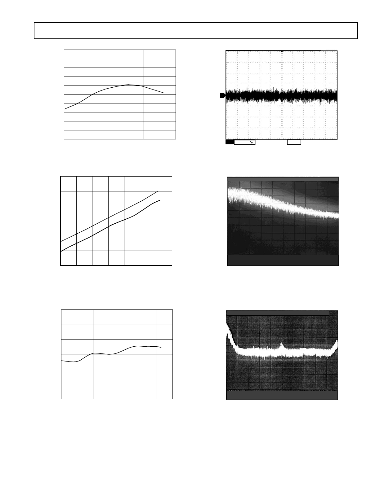
TPC 1. V
vs. Temperature
OUT
TPC 2. Supply Current vs. Temperature
TPC 4. Noise Voltage Peak-to-Peak 10 Hz to 10 kHz
TPC 5. Output Noise Density Plot
(VIN = 3.6 V, C
= 1 µF, CIN = 1 µF)
OUT
TPC 3. Line Regulation vs. Temperature
TPC 6. Voltage Noise Density 0 Hz to 100 kHz
–3–
 Loading...