ANALOG DEVICES ADR1581 Service Manual

1.25 V Micropower, Precision Shunt
V
V
www.BDTIC.com/ADI
FEATURES
Wide operating range: 60 μA to 10 mA
Initial accuracy: ±0.12% maximum
Temperature drift: ±50 ppm/°C maximum
Output impedance: 0.5 Ω maximum
Wideband noise (10 Hz to 10 kHz): 20 μV rms
Operating temperature range: −40°C to +85°C
High ESD rating
4 kV human body model
400 V machine model
Compact, surface-mount SOT-23 package
APPLICATIONS
Portable, battery-powered equipment
Cellular phones, notebook computers, PDAs, GPSs,
and DMMs
Computer workstations
Suitable for use with a wide range of video RAMDACs
Smart industrial transmitters
PCMCIA cards
Automotive
3 V/5 V, 8-bit to 12-bit data converters
GENERAL DESCRIPTION
The ADR15811 is a low cost, 2-terminal (shunt), precision band
gap reference. It provides an accurate 1.250 V output for input
currents between 60 A and 10 mA.
The superior accuracy and stability of the ADR1581 is made
possible by the precise matching and thermal tracking of onchip components. Proprietary curvature correction design
techniques have been used to minimize the nonlinearities in
the voltage output temperature characteristics. The ADR1581
is stable with any value of capacitive load.
The low minimum operating current makes the ADR1581 ideal
fo
r use in battery-powered 3 V or 5 V systems. However, the wide
operating current range means that the ADR1581 is extremely
versatile and suitable for use in a wide variety of high current
applications.
The ADR1581 is available in two grades, A and B, both of which
re provided in the SOT-23 package. Both grades are specified
a
over the industrial temperature range of −40°C to +85°C.
1
Protected by U.S. Patent No. 5,969,657; other patents pending.
Voltage Reference
ADR1581
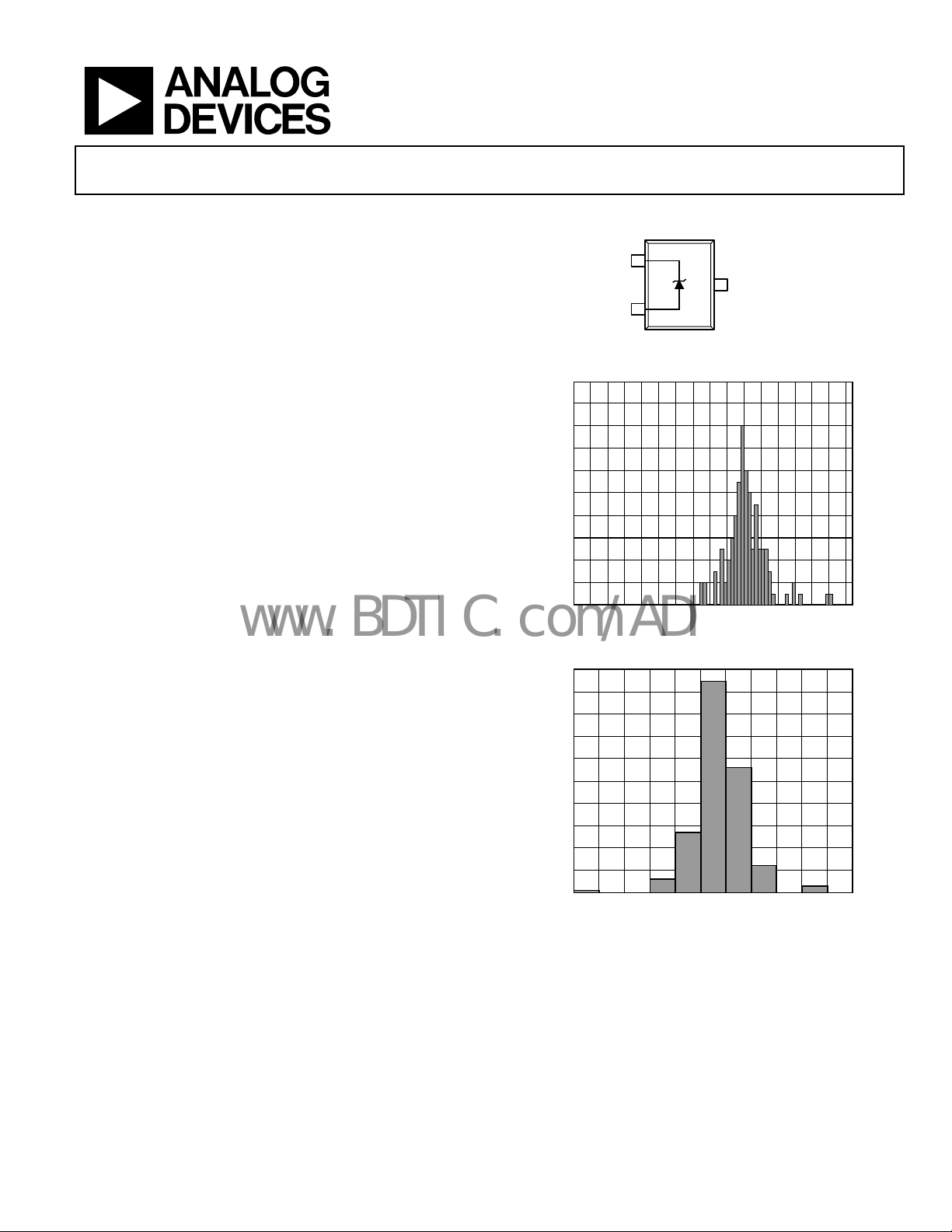
PIN CONFIGURATION
ADR1581
1
+
NC (OR V–)
3
–
2
TOP VIEW
NC = NO CONNECT
Figure 1. SOT-23
20
18
16
14
12
10
QUANTITY
8
6
4
2
0
–20 –10 0 10 20
Figure 2. Reverse Voltage Temperature Drift Distribution
100
90
80
70
60
50
QUANTITY
40
30
20
10
0
–5 –4 –3 –2 –1 0 1 2 3 4 5
TEMPERATURE DRIFT (ppm/°C)
OUTPUT ERROR (mV)
Figure 3. Reverse Voltage Error Distribution
06672-001
06672-002
06672-003
Rev. 0
Information furnished by Analog Devices is believed to be accurate and reliable. However, no
responsibility is assumed by Anal og Devices for its use, nor for any infringements of patents or ot her
rights of third parties that may result from its use. Specifications subject to change without notice. No
license is granted by implication or otherwise under any patent or patent rights of Analog Devices.
Trademarks and registered trademarks are the property of their respective owners.
One Technology Way, P.O. Box 9106, Norwood, MA 02062-9106, U.S.A.
Tel: 781.329.4700 www.analog.com
Fax: 781.461.3113 ©2007 Analog Devices, Inc. All rights reserved.

ADR1581
www.BDTIC.com/ADI
TABLE OF CONTENTS
Features.............................................................................................. 1
Temperature Performance............................................................6
Applications....................................................................................... 1
General Description ......................................................................... 1
Pin Configuration............................................................................. 1
Revision History ............................................................................... 2
Specifications..................................................................................... 3
Absolute Maximum Ratings............................................................ 4
ESD Caution.................................................................................. 4
Typical Performance Characteristics ............................................. 5
Theory of Operation ........................................................................ 6
Applying the ADR1581................................................................ 6
REVISION HISTORY
5/07—Revision 0: Initial Version
Voltage Output Nonlinearity vs. Temperature..........................7
Reverse Voltage Hysteresis...........................................................7
Output Impedance vs. Frequency ...............................................8
Noise Performance and Reduction .............................................8
Turn-On Time ...............................................................................8
Transient Response .......................................................................9
Precision Micropower Low Dropout Reference .......................9
Using the ADR1581 with 3 V Data Converters ..................... 10
Outline Dimensions....................................................................... 11
Ordering Guide .......................................................................... 12
Rev. 0 | Page 2 of 12

ADR1581
www.BDTIC.com/ADI
SPECIFICATIONS
TA = 25°C, IIN = 100 µA, unless otherwise noted.
Table 1.
ADR1581A ADR1581B
Parameter Min Typ Max Min Typ Max Unit
REVERSE VOLTAGE OUTPUT (SOT-23) 1.240 1.250 1.260 1.2485 1.250 1.2515 V
REVERSE VOLTAGE TEMPERATURE DRIFT
−40°C to +85°C 100 50 ppm/°C
MINIMUM OPERATING CURRENT, T
MIN
to T
60 60 A
MAX
REVERSE VOLTAGE CHANGE WITH REVERSE CURRENT
60 A < IIN < 10 mA, T
60 A < IIN < 1 mA, T
MIN
MIN
to T
2.5 6 2.5 6 mV
MAX
to T
0.8 0.8 mV
MAX
DYNAMIC OUTPUT IMPEDANCE (VR/∆IR)
IIN = 1 mA ± 100 A (f = 120 Hz) 0.4 1 0.4 0.5 Ω
OUTPUT NOISE
RMS Noise Voltage: 10 Hz to 10 kHz 20 20 V rms
Low Frequency Noise Voltage: 0.1 Hz to 10 Hz 4.5 4.5 V p-p
TURN-ON SETTLING TIME TO 0.1%
OUTPUT VOLTAGE HYSTERESIS
1
2
5 5 µs
80 80 µV
TEMPERATURE RANGE
Specified Performance, T
Operating Range
1
Measured with a no load capacitor.
2
Output hysteresis is defined as the change in the +25°C output voltage after a temperature excursion to −40°C, then to +85°C, and back to +25°C.
3
The operating temperature range is defined as the temperature extremes at which the device continues to function. Parts may deviate from their specified
performance.
3
MIN
to T
−40 +85 −40 +85 °C
MAX
−55 +125 −55 +125 °C
Rev. 0 | Page 3 of 12

ADR1581
www.BDTIC.com/ADI
ABSOLUTE MAXIMUM RATINGS
Table 2.
Parameter Rating
Reverse Current 25 mA
Forward Current 20 mA
Internal Power Dissipation
SOT-23 (RT) 0.3 W
Storage Temperature Range −65°C to +150°C
Operating Temperature Range
ADR1581/RT −55°C to +125°C
Lead Temperature, Soldering
Vapor Phase (60 sec) 215°C
Infrared (15 sec) 220°C
ESD Susceptibility2
Human Body Model 4 kV
Machine Model 400 V
1
Specification is for device (SOT-23 package) in free air at 25°C: θJA = 300°C/W.
2
The human body model is a 100 pF capacitor discharged through 1.5 kΩ. For
the machine model, a 200 pF capacitor is discharged directly into the device.
1
Stresses above those listed under Absolute Maximum Ratings
may cause permanent damage to the device. This is a stress
rating only; functional operation of the device at these or any
other conditions above those indicated in the operational
section of this specification is not implied. Exposure to absolute
maximum rating conditions for extended periods may affect
device reliability.
ESD CAUTION
Rev. 0 | Page 4 of 12
 Loading...