Precision Series Sub-Band Gap
www.BDTIC.com/ADI
FEATURES
Initial accuracy
A grade: +
B grade: +
Maximum temperature coefficient
A grade: 50 ppm/°C
B grade: 25 ppm/°C
C
= 50 nF to 10 µF
LOAD
Output current: +4 mA/−2 mA
Low operating current: 80 A (typical)
Output noise: 6 µV p-p @ 1.0 V output
Input range: 2.0 V to 18 V
Temperature range: −40°C to +125°C
Tiny, Pb-free TSOT package
APPLICATIONS
Battery-powered instrumentation
Portable medical equipment
Communication infrastructure equipment
0.70% (maximum)
0.35% (maximum)
Voltage Reference
ADR130
PIN CONFIGURATION
1
NC
ADR130
TOP VIEW
2
GND
(Not to Scale)
3
V
IN
NC = NO CONNECT
Figure 1. 6-Lead TSOT (UJ-6)
NC
6
5
SET
4
V
OUT
06322-001
GENERAL DESCRIPTION
The ADR130 is the industry’s first family of tiny, micropower,
low voltage, high precision voltage references. Featuring 0.35%
initial accuracy and 25 ppm/°C of temperature drift in the tiny
TSOT-23 package, the ADR130 voltage reference only requires
80 μA for typical operation. The ADR130 design includes a
patented temperature drift curvature correction technique that
minimizes the nonlinearities in the output voltage vs. temperature characteristics.
Available in the industrial temperature range of −40°C to
+125°C, the ADR130 is housed in a tiny TSOT package.
For 0.5 V output, tie SET (Pin 5) to V
(Pin 4). For 1.0 V
OUT
output, tie SET (Pin 5) to GND (Pin 2).
Rev. 0
Information furnished by Analog Devices is believed to be accurate and reliable. However, no
responsibility is assumed by Anal og Devices for its use, nor for any infringements of patents or ot her
rights of third parties that may result from its use. Specifications subject to change without notice. No
license is granted by implication or otherwise under any patent or patent rights of Analog Devices.
Trademarks and registered trademarks are the property of their respective owners.
One Technology Way, P.O. Box 9106, Norwood, MA 02062-9106, U.S.A.
Tel: 781.329.4700 www.analog.com
Fax: 781.461.3113 ©2006 Analog Devices, Inc. All rights reserved.

ADR130
www.BDTIC.com/ADI
TABLE OF CONTENTS
Features .............................................................................................. 1
Applications....................................................................................... 1
Pin Configuration............................................................................. 1
General Description......................................................................... 1
Revision History ............................................................................... 2
Specifications..................................................................................... 3
Electrical Characteristics............................................................. 3
Absolute Maximum Ratings............................................................ 5
Thermal Resistance ...................................................................... 5
ESD Caution.................................................................................. 5
Typical Performance Characteristics ............................................. 6
Te r mi n ol o g y .................................................................................... 11
REVISION HISTORY
10/06—Revision 0: Initial Version
Theory of Operation ...................................................................... 12
Power Dissipation Considerations ........................................... 12
Input Capacitor........................................................................... 12
Output Capacitor........................................................................ 12
Application Notes........................................................................... 13
Basic Voltage Reference Connection....................................... 13
Stacking Reference ICs for Arbitrary Outputs ....................... 13
Negative Precision Reference Without Precision Resistors.. 14
Precision Current Source .......................................................... 14
Outline Dimensions ....................................................................... 15
Ordering Guide .......................................................................... 15
Rev. 0 | Page 2 of 16

ADR130
www.BDTIC.com/ADI
SPECIFICATIONS
ELECTRICAL CHARACTERISTICS
TA = 25°C, VIN = 2.0 V to 18 V, unless otherwise noted. SET (Pin 5) tied to V
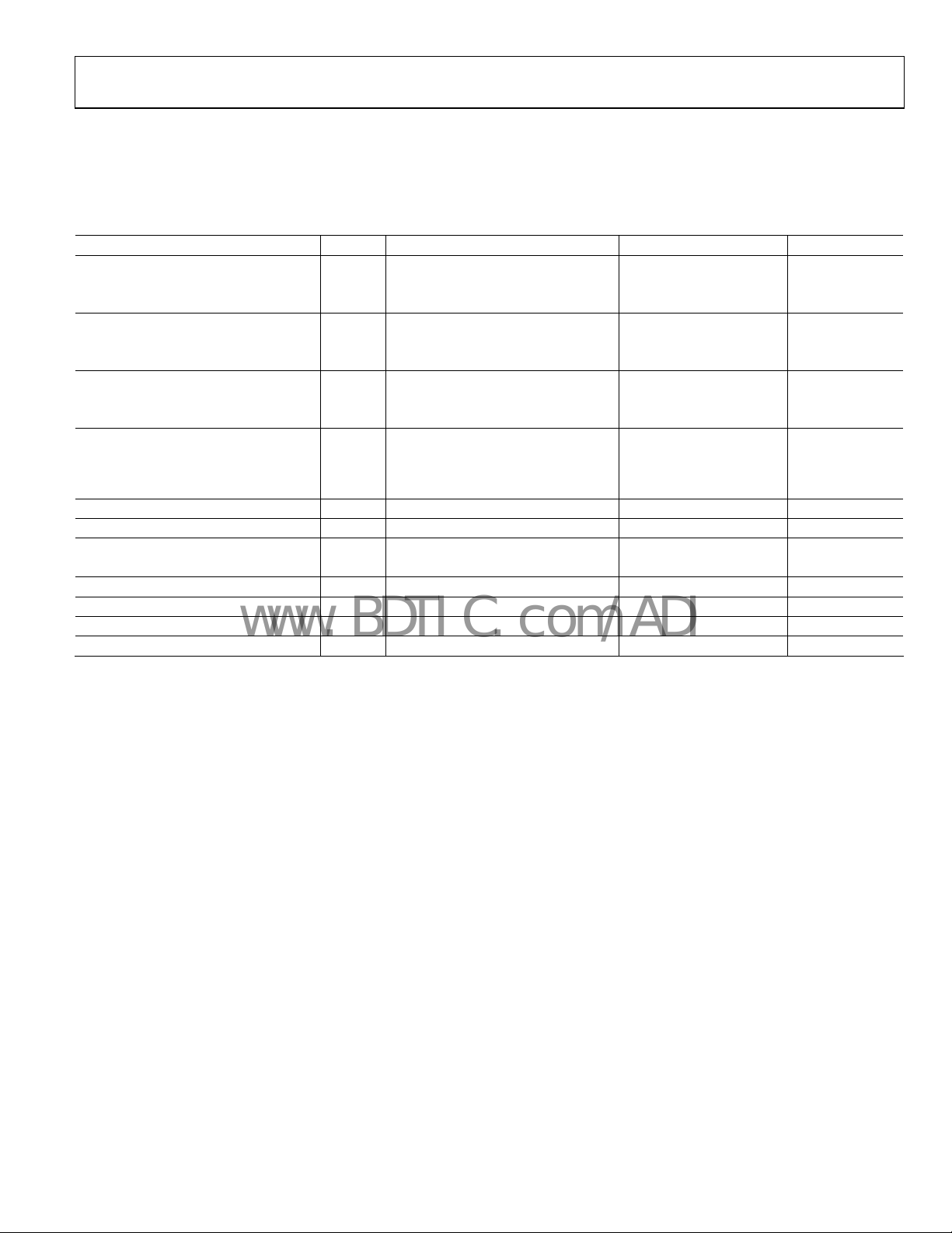
Table 1.
Parameter Symbol Conditions Min Typ Max Unit
OUTPUT VOLTAGE V
A Grade 0.49650 0.5 0.50350 V
B Grade 0.49825 0.5 0.50175 V
INITIAL ACCURACY ERROR V
A Grade −3.50 +3.50 mV
B Grade −1.75 +1.75 mV
TEMPERATURE COEFFICIENT TCV
A Grade 15 50 ppm/°C
B Grade 5 25 ppm/°C
LOAD REGULATION
LINE REGULATION 2.0 V to 18 V, I
QUIESCENT CURRENT I
SHORT-CIRCUIT CURRENT TO GROUND VIN = 2.0 V 15 mA
V
VOLTAGE NOISE 0.1 Hz to 10 Hz 3 μV p-p
TURN-ON SETTLING TIME To 0.1%, CL = 0.1 μF 80 μs
LONG-TERM STABILITY 1000 hours @ 25°C 100 ppm/1000 hours
OUTPUT VOLTAGE HYSTERESIS 150 ppm
O
OERR
Q
−40°C < TA < +125°C
O
−40°C < T
0 mA < I
−40°C < T
−2 mA < I
−40°C < TA < +125°C, no load 75 150 μA
IN
< +125°C; 3 V ≤ VIN ≤ 18 V;
A
< 4 mA
OUT
< +125°C; 3 V ≤ VIN ≤ 18 V;
A
< 0 mA
OUT
= 0 mA −40 +10 +40 ppm/V
OUT
= 18.0 V 50 mA
(Pin 4).
OUT
−0.13 +0.13 mV/mA
−1.0 +1.0 mV/mA
Rev. 0 | Page 3 of 16

ADR130
www.BDTIC.com/ADI
TA = 25°C, VIN = 2.0 V to 18 V, unless otherwise noted. SET (Pin 5) tied to GND (Pin 2).
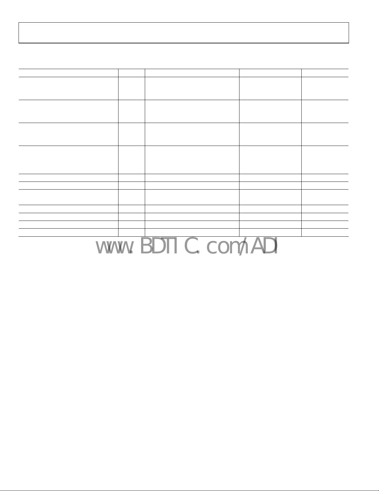
Table 2.
Parameter Symbol Conditions Min Typ Max Unit
OUTPUT VOLTAGE V
O
A Grade 0.9930 1.0 1.0070 V
B Grade 0.9965 1.0 1.0035 V
INITIAL ACCURACY ERROR V
OERR
A Grade −7.0 +7.0 mV
B Grade −3.5 +3.5 mV
TEMPERATURE COEFFICIENT TCV
A Grade 15 50 ppm/°C
B Grade 5 25 ppm/°C
LOAD REGULATION
LINE REGULATION 2.0 V to 18 V, I
QUIESCENT CURRENT I
Q
SHORT-CIRCUIT CURRENT TO GROUND VIN = 2.0 V 15 mA
V
VOLTAGE NOISE 0.1 Hz to 10 Hz 6 μV p-p
TURN-ON SETTLING TIME To 0.1%, CL = 0.1 μF 80 μs
LONG-TERM STABILITY 1000 hours @ 25°C 100 ppm/1000 hours
OUTPUT VOLTAGE HYSTERESIS 150 ppm
−40°C < TA < +125°C
O
−40°C < T
0 mA < I
−40°C < T
−2 mA < I
< +125°C; 3 V ≤ VIN ≤ 18 V;
A
< 4 mA
OUT
< +125°C; 3 V ≤ VIN ≤ 18 V;
A
< 0 mA
OUT
= 0 mA −40 +10 +40 ppm/V
OUT
−0.25 +0.25 mV/mA
−2.0 +2.0 mV/mA
−40°C < TA < +125°C, no load 85 150 μA
= 18.0 V 50 mA
IN
Rev. 0 | Page 4 of 16

ADR130
www.BDTIC.com/ADI
ABSOLUTE MAXIMUM RATINGS
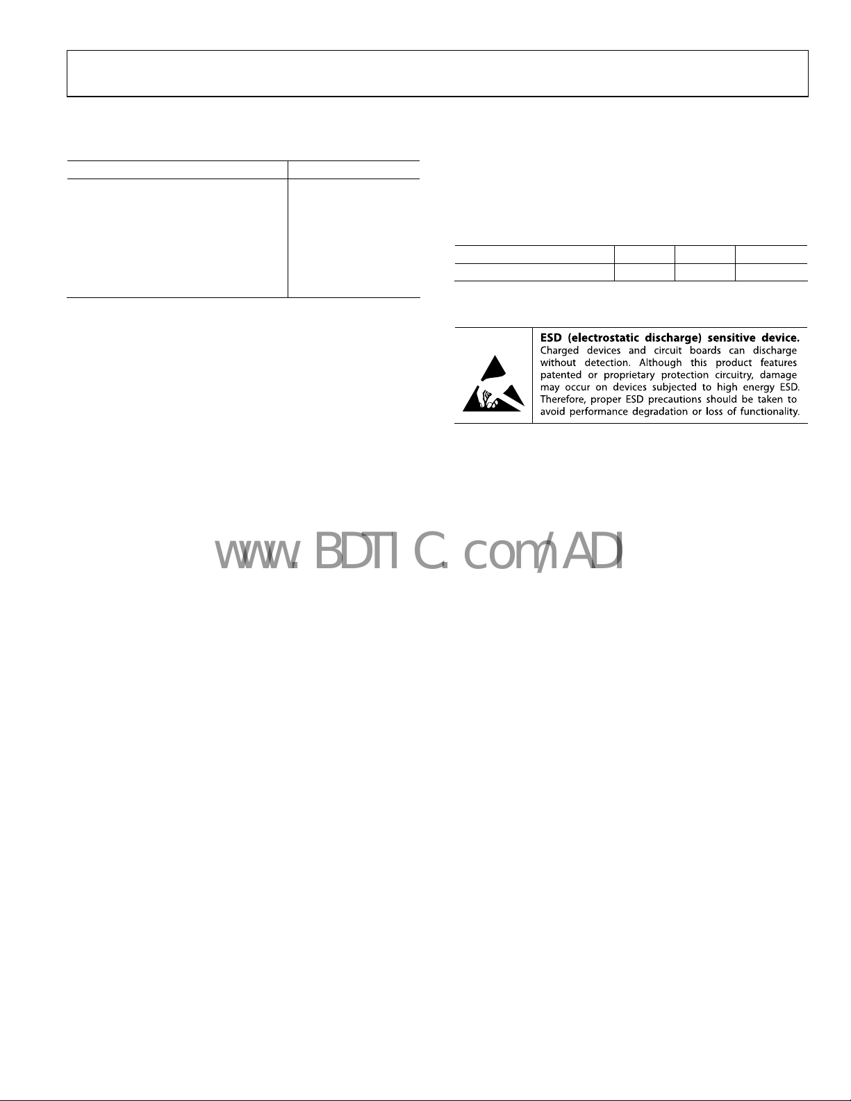
Table 3.
Parameter Ratings
VIN to GND 20 V
Internal Power Dissipation 40 mW
Storage Temperature Range −65°C to +150°C
Specified Temperature Range −40°C to +120°C
Lead Temperature, Soldering
Vapor Phase (60 sec) 215°C
Infrared (15 sec) 220°C
Stresses above those listed under Absolute Maximum Ratings
may cause permanent damage to the device. This is a stress
rating only; functional operation of the device at these or any
other conditions above those indicated in the operational
section of this specification is not implied. Exposure to absolute
maximum rating conditions for extended periods may affect
device reliability.
THERMAL RESISTANCE
θJA is specified for the worst-case conditions, that is, a device
soldered in a circuit board for surface-mount packages.
Table 4. Thermal Resistance
Package Type θ
TSOT (UJ-6) 186 67 °C/W
JA
θ
JC
Unit
ESD CAUTION
Rev. 0 | Page 5 of 16
 Loading...