Precision, Micropower LDO Voltage
www.BDTIC.com/ADI
FEATURES
Initial accuracy
A grade: ±0.24%
B grade: ±0.12%
Maximum temperature coefficient
A grade: 25 ppm/°C
B grade: 9 ppm/°C
Low dropout: 300 mV for ADR121/ADR125
High output current: +5 mA/−2 mA
Low typical operating current: 85 μA
Input range: 2.7 V to 18 V for ADR127
Temperature range: −40°C to +125°C
Tiny TSOT (UJ-6) package
APPLICATIONS
Battery-powered instrumentation
Portable medical equipment
Data acquisition systems
Automotive
References in TSOT
ADR121/ADR125/ADR127
PIN CONFIGURATION
1
1
NC
GND
ADR12x
2
TOP VIEW
(Not to Scale)
V
3
IN
NC = NO CONNECT
1
MUST BE LEFT FLOATING
Figure 1.
1
6
NC
1
NC
5
V
4
OUT
05725-001
GENERAL DESCRIPTION
The ADR121/ADR125/ADR127 are a family of micropower,
high precision, series mode, band gap references with sink and
source capability. The parts feature high accuracy and low
power consumption in a tiny package. The ADR12x design
includes a patented temperature-drift curvature correction
technique that minimizes the nonlinearities in the output
voltage vs. temperature characteristics.
The ADR12x is a low dropout voltage reference, requiring only
300 mV for the ADR121/ADR125 and 1.45 V for the ADR127
above the nominal output voltage on the input to provide a
stable output voltage. This low dropout performance, coupled
with the low 85 μA operating current, makes the ADR12x ideal
for battery-powered applications.
Available in an extended industrial temperature range of −40°C
to +125°C, the ADR121/ADR125/ADR127 are housed in the
tiny TSOT (UJ-6) package.
Rev. B
Information furnished by Analog Devices is believed to be accurate and reliable. However, no
responsibility is assumed by Analog Devices for its use, nor for any infringements of patents or other
rights of third parties that may result from its use. Specifications subject to change without notice. No
license is granted by implication or otherwise under any patent or patent rights of Analog Devices.
Trademarks and registered trademarks are the property of their respective owners.
One Technology Way, P.O. Box 9106, Norwood, MA 02062-9106, U.S.A.
Tel: 781.329.4700 www.analog.com
Fax: 781.461.3113 ©2006–2008 Analog Devices, Inc. All rights reserved.

ADR121/ADR125/ADR127
www.BDTIC.com/ADI
TABLE OF CONTENTS
Features .............................................................................................. 1
Applications ....................................................................................... 1
Pin Configuration ............................................................................. 1
General Description ......................................................................... 1
Revision History ............................................................................... 2
Specifications ..................................................................................... 3
ADR121 Electrical Characteristics ............................................. 3
ADR125 Electrical Characteristics ............................................. 4
ADR127 Electrical Characteristics ............................................. 5
Absolute Maximum Ratings ............................................................ 6
Thermal Resistance ...................................................................... 6
ESD Caution .................................................................................. 6
Typical Performance Characteristics ............................................. 7
REVISION HISTORY
1/08—Rev. A to Rev. B
Changes to Table 1 ............................................................................ 3
Changes to Table 2 ............................................................................ 4
Changes to Table 3 .............................................................................5
Changes to Figure 52 ...................................................................... 17
Changes to Ordering Guide ......................................................... 18
Terminology .................................................................................... 15
Theory of Operation ...................................................................... 16
Power Dissipation Considerations ........................................... 16
Input Capacitor ........................................................................... 16
Output Capacitor ........................................................................ 16
Applications Information .............................................................. 17
Basic Voltage Reference Connection ....................................... 17
Stacking Reference ICs for Arbitrary Outputs ....................... 17
Negative Precision Reference Without Precision Resistors .. 17
General-Purpose Current Source ............................................ 17
Outline Dimensions ....................................................................... 18
Ordering Guide .......................................................................... 18
5/07—Rev. 0 to Rev. A
Changes to Table 1 ............................................................................ 3
Changes to Table 2 ............................................................................ 4
Changes to Table 3 ............................................................................ 5
Added Thermal Hysteresis Equation ............................................. 7
Changes to Ordering Guide .......................................................... 18
6/06—Revision 0: Initial Version
Rev. B | Page 2 of 20

ADR121/ADR125/ADR127
www.BDTIC.com/ADI
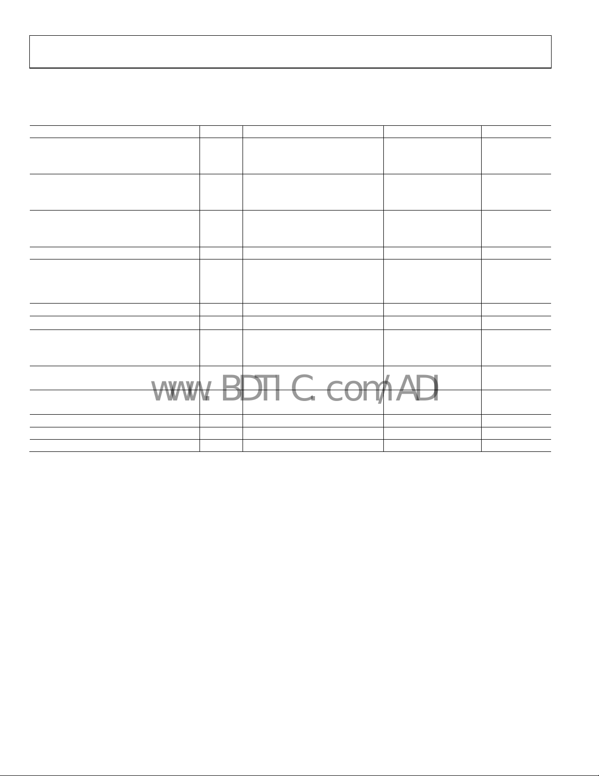
SPECIFICATIONS
ADR121 ELECTRICAL CHARACTERISTICS
TA = 25°C, VIN = 2.8 V to 18 V, I
Table 1.
Parameter Symbol Conditions/Comments Min Typ Max Unit
OUTPUT VOLTAGE V
B Grade 2.497 2.5 2.503 V
A Grade 2.494 2.5 2.506 V
INITIAL ACCURACY ERROR V
B Grade −0.12 +0.12 %
A Grade −0.24 +0.24 %
TEMPERATURE COEFFICIENT TCV
B Grade 3 9 ppm/°C
A Grade 15 25 ppm/°C
DROPOUT (V
− VIN) VDO I
OUT
LOAD REGULATION
LINE REGULATION 2.8 V to 18 V, I
PSRR f = 60 Hz −90 dB
QUIESCENT CURRENT IQ −40°C < TA < +125°C, no load
V
V
SHORT-CIRCUIT CURRENT TO GROUND VIN = 2.8 V 18 mA
V
VOLTAGE NOISE f = 10 kHz 500 nV/√Hz
f = 0.1 Hz to 10 Hz 18 μV p-p
TURN-ON SETTLING TIME To 0.1%, CL = 0.2 μF 100 μs
LONG-TERM STABILITY 1000 hours @ 25°C 150 ppm/1000 hrs
OUTPUT VOLTAGE HYSTERESIS See the Terminology section 300 ppm
= 0 mA, unless otherwise noted.
OUT
OUT
OERR
−40°C < TA < +125°C
OUT
OUT
−40°C < T
0 mA < I
−40°C < T
−2 mA < I
= 0 mA 300 mV
< +125°C; VIN = 5.0 V,
A
< 5 mA
OUT
< +125°C; VIN = 5.0 V,
A
< 0 mA
OUT
= 0 mA −50 +3 +50 ppm/V
OUT
= 18 V 95 125 μA
IN
= 2.8 V 80 95 μA
IN
= 18 V 40 mA
IN
80 300 ppm/mA
50 300 ppm/mA
Rev. B | Page 3 of 20

ADR121/ADR125/ADR127
www.BDTIC.com/ADI
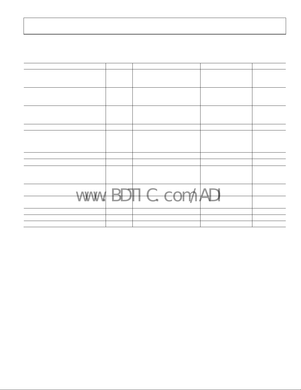
ADR125 ELECTRICAL CHARACTERISTICS
TA = 25°C, VIN = 5.3 V to 18 V, I
Table 2.
Parameter Symbol Conditions/Comments Min Typ Max Unit
OUTPUT VOLTAGE V
B Grade 4.994 5.0 5.006 V
A Grade 4.988 5.0 5.012 V
INITIAL ACCURACY ERROR V
B Grade −0.12 +0.12 %
A Grade −0.24 +0.24 %
TEMPERATURE COEFFICIENT TCV
B Grade 3 9 ppm/°C
A Grade 15 25 ppm/°C
DROPOUT (V
− VIN) VDO I
OUT
LOAD REGULATION
LINE REGULATION 5.3 V to 18 V, I
PSRR
QUIESCENT CURRENT IQ −40°C < TA < +125°C, no load
V
V
SHORT-CIRCUIT CURRENT TO GROUND VIN = 5.3 V 25 mA
V
VOLTAGE NOISE f = 10 kHz 900 nV/√Hz
f = 0.1 Hz to 10 Hz 36 μV p-p
TURN-ON SETTLING TIME To 0.1%, CL = 0.2 μF 100 μs
LONG-TERM STABILITY 1000 hours @ 25°C 150 ppm/1000 hrs
OUTPUT VOLTAGE HYSTERESIS See the Terminology section 300 ppm
= 0 mA, unless otherwise noted.
OUT
OUT
OERR
−40°C < TA < +125°C
OUT
OUT
−40°C < T
0 mA < I
−40°C < T
−2 mA < I
f = 60 Hz −90 dB
= 18 V 95 125 μA
IN
= 5.3 V 80 95 μA
IN
= 18 V 40 mA
IN
= 5 mA 300 mV
< +125°C; VIN = 6.0 V,
A
< 5 mA
OUT
< +125°C; VIN = 6.0 V,
A
< 0 mA
OUT
= 0 mA 30 ppm/V
OUT
35 200 ppm/mA
35 200 ppm/mA
Rev. B | Page 4 of 20

ADR121/ADR125/ADR127
www.BDTIC.com/ADI
ADR127 ELECTRICAL CHARACTERISTICS
TA = 25°C, VIN = 2.7 V to 18 V, I
Table 3.
Parameter Symbol Conditions/Comments Min Typ Max Unit
OUTPUT VOLTAGE V
B Grade 1.2485 1.25 1.2515 V
A Grade 1.2470 1.25 1.2530 V
INITIAL ACCURACY ERROR V
B Grade −0.12 +0.12 %
A Grade −0.24 +0.24 %
TEMPERATURE COEFFICIENT TCV
B Grade 3 9 ppm/°C
A Grade 15 25 ppm/°C
DROPOUT (V
− VIN) VDO I
OUT
LOAD REGULATION
LINE REGULATION 2.7 V to 18 V, I
PSRR
QUIESCENT CURRENT IQ −40°C < TA < +125°C, no load
V
V
SHORT-CIRCUIT CURRENT TO GROUND VIN = 2.7 V 15 mA
V
VOLTAGE NOISE f = 10 kHz 300 nV/√Hz
f = 0.1 Hz to 10 Hz 9 μV p-p
TURN-ON SETTLING TIME To 0.1%, CL = 0.2 μF 80 μs
LONG-TERM STABILITY 1000 hours @ 25°C 150 ppm/1000 hrs
OUTPUT VOLTAGE HYSTERESIS See the Terminology section 300 ppm
= 0 mA, unless otherwise noted.
OUT
OUT
OERR
−40°C < TA < +125°C
OUT
OUT
−40°C < T
0 mA < I
−40°C < T
−2 mA < I
f = 60 Hz −90 dB
IN
IN
IN
= 0 mA 1.45 V
< +125°C; VIN = 3.0 V,
A
< 5 mA
OUT
< +125°C; VIN = 3.0 V,
A
< 0 mA
OUT
= 0 mA 30 90 ppm/V
OUT
85 400 ppm/mA
65 400 ppm/mA
= 18 V 95 125 μA
= 2.7 V 80 95 μA
= 18 V 30 mA
Rev. B | Page 5 of 20

ADR121/ADR125/ADR127
www.BDTIC.com/ADI
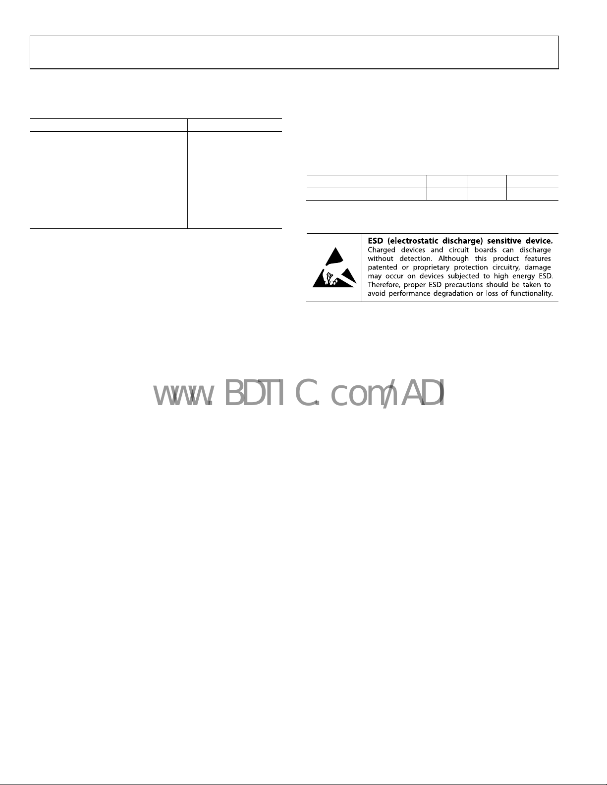
ABSOLUTE MAXIMUM RATINGS
Table 4.
Parameter Rating
VIN to GND 20 V
Internal Power Dissipation
TSOT (UJ-6) 40 mW
Storage Temperature Range −65°C to +150°C
Operating Temperature Range −40°C to +125°C
Lead Temperature, Soldering
Vapor Phase (60 sec) 215°C
Infrared (15 sec) 220°C
Stresses above those listed under Absolute Maximum Ratings
may cause permanent damage to the device. This is a stress
rating only; functional operation of the device at these or any
other conditions above those indicated in the operational
section of this specification is not implied. Exposure to absolute
maximum rating conditions for extended periods may affect
device reliability.
THERMAL RESISTANCE
θJA is specified for the worst-case conditions, that is, a device
soldered in a circuit board for surface-mount packages.
Table 5.
Package Type θJA θ
6-Lead TSOT (UJ-6) 230 146 °C/W
Unit
JC
ESD CAUTION
Rev. B | Page 6 of 20
 Loading...