Charge-Pump, Parallel Backlight Driver
V
FEATURES
Charge pump with automatic gain selection of 1×, 1.5×, and
2× for maximum efficiency
Two high accuracy (±5%) phototransistor inputs for
automated ambient light sensing (ALS)
5 programmable ambient light-sensing zones for optimal
backlight power savings
Independent ALS control of D7, for automated response of
keypad lighting to ambient light levels
PWM input can be used for content adaptive brightness
control (CABC) of any, or all, of the LEDs
with Image Content PWM Input
ADP8870
APPLICATIONS
Mobile display backlighting
Mobile phone keypad backlighting
RGB LED lighting
LED indication
General backlighting of small format displays
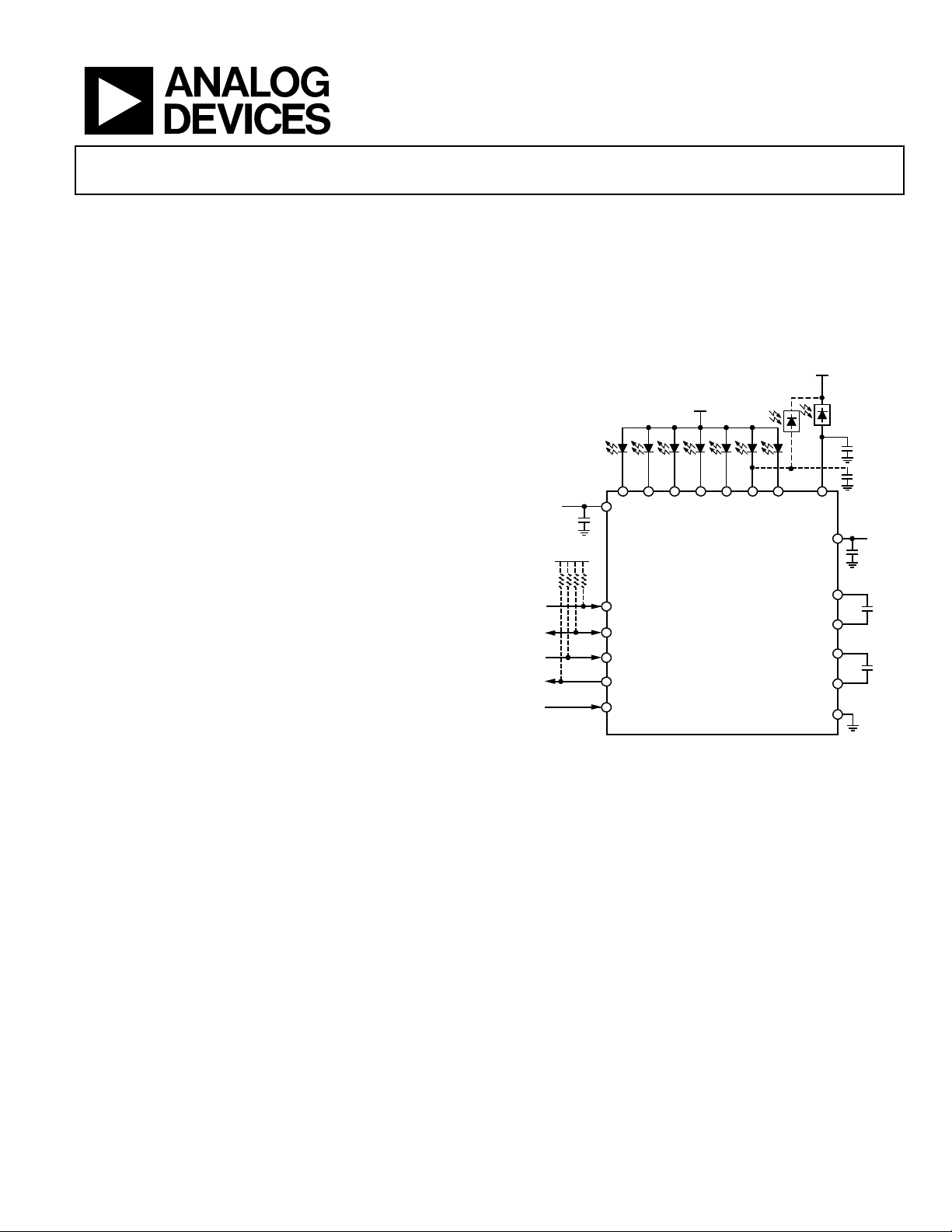
TYPICAL OPERATING CIRCUIT
OPTIONAL
V
PHOTOSENSOR
OUT
DD_ALS
PWM input scales the LED output current
7 independent, programmable LED drivers
6 drivers capable of 30 mA (maximum)
1 driver capable of 60 mA (maximum)
Programmable maximum current limit (128 levels)
Standby mode for <1 μA current consumption
16 programmable fade-in and fade-out times (0.1 sec to 5.5 sec)
with choice of square or cubic rates
V
IN
1µF
VDDIO
D1 D2 D3 D4 D5 D6 D7 CMP_IN
Fading override
2
I
C-compatible interface for all programming
Dedicated reset pin and built-in power-on reset (POR)
Short-circuit, overvoltage, and overtemperature protection
Internal soft start to limit inrush currents
Input-to-output isolation during faults or shutdown
Operates down to V
= 2.5 V, with undervoltage lockout
IN
(UVLO) at 2.0 V.
nRST
SDA
SCL
nINT
PWM
ADP8870
Available in a small, 2.15 mm × 2.36 mm × 0.6 mm wafer level
chip scale package (WLCSP) or a 4 mm × 4 mm × 0.75 mm
Figure 1.
lead frame chip scale package (LFCSP)
GENERAL DESCRIPTION
The ADP8870 combines a programmable backlight LED
charge-pump driver with automatic phototransistor control of
the brightness (LED current) and a PWM input to control the
scale of the output current. This combination allows significant
power savings because it automatically changes the current
intensity based on the sensed ambient lighting levels and the
display image content. It performs this function automatically,
eliminating the need for a processor to monitor the phototransistor. The light intensity thresholds are fully programmable
via the I
2
C interface.
The ADP8870 allows up to six LEDs to be independently driven up
to 30 mA (maximum). An additional seventh LED can be driven to
For more information about the ADP8870, including the complete data sheet, contact your local Analog Devices, Inc., sales office at
www.analog.com/sales.
Rev. Sp0
Information furnished by Analog Devices is believed to be accurate and reliable. However, no
responsibility is assumed by Analog Devices for its use, nor for any infringements of patents or other
rights of third parties that may result from its use. Specifications subject to change without notice. No
license is granted by implication or otherwise under any patent or patent rights of Analog Devices.
Trademarks and registered trademarks are the property of their respective owners.
60 mA (maximum). All LEDs are individually programmable for
minimum/maximum current and fade-in/fade-out times through
2
an I
C interface. These LEDs can also be combined into groups
to reduce the processor instructions during fade-in and fade-out.
Driving these components is a two-capacitor charge pump
with gains of 1×, 1.5×, and 2×. This setup is capable of driving a
maximum I
of 240 mA from a supply of 2.5 V to 5.5 V. A full
OUT
suite of safety features, including short-circuit, overvoltage, and
overtemperature protection, allows easy implementation of a
safe and robust design. Additionally, input inrush currents are
limited via an integrated soft start combined with controlled
input-to-output isolation.
One Technology Way, P.O. Box 9106, Norwood, MA 02062-9106, U.S.A.
Tel: 781.329.4700 www.analog.com
Fax: 781.461.3113 ©2010 Analog Devices, Inc. All rights reserved.
PHOTOSENSOR
0.1µF
0.1µF
1µF
C1+
C1–
C2+
C2–
GND
V
OUT
C1
1µF
C2
1µF
08829-001

ADP8870
OUTLINE DIMENSIONS
2.190
2.150
2.110
4
1
23
BALL 1
IDENTIFIER
0.645
0.600
0.555
SEATING
PLANE
INDICATOR
SEATING
PIN 1
0.80
0.75
0.70
PLANE
2.395
TOP VIEW
(BALL SIDE DOWN)
SIDE VIEW
0.287
0.267
0.247
2.355
2.315
0.415
0.400
0.385
1.60 REF
0.40
REF
COPLANARITY
0.05
0.230
0.200
0.170
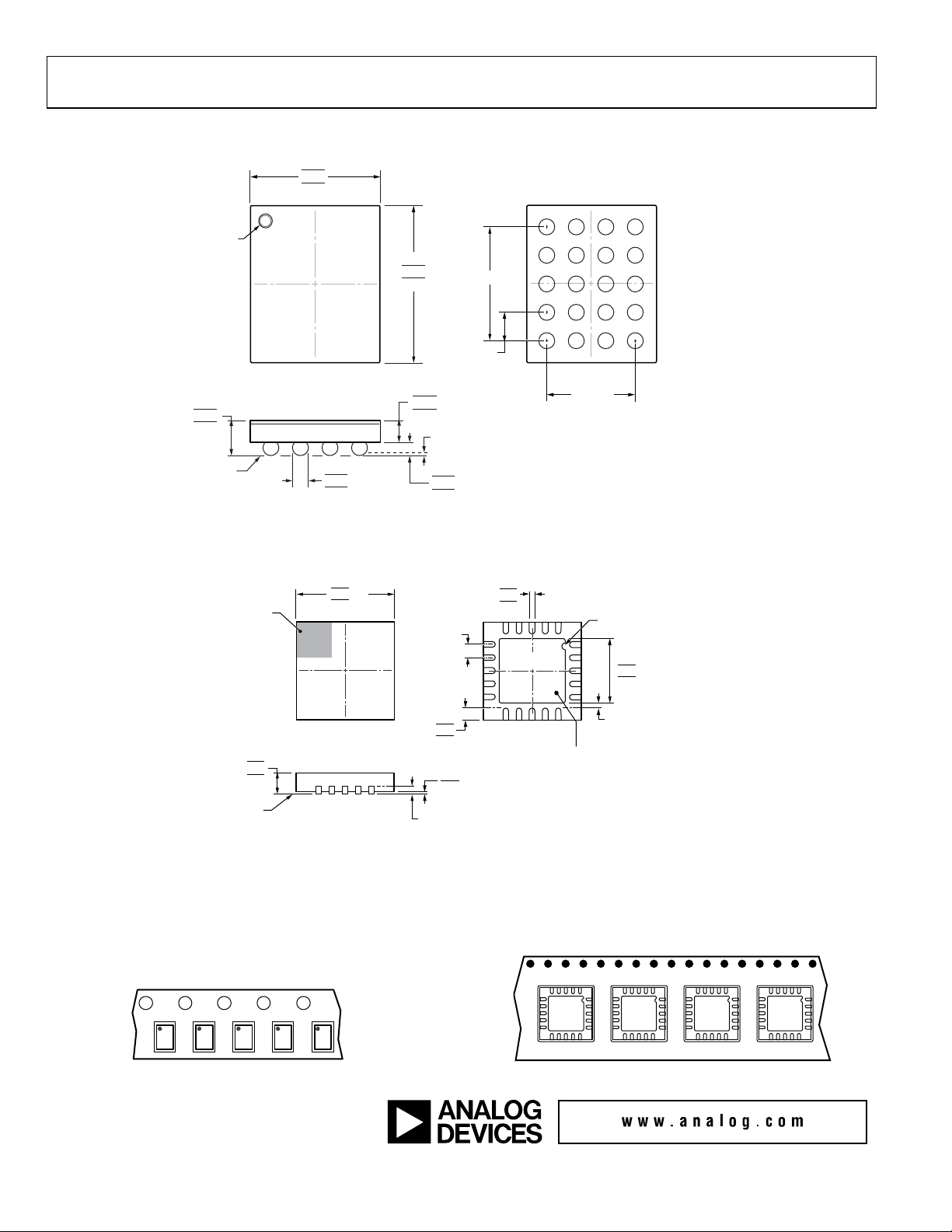
Figure 2. 20-Ball Wafer Level Chip Scale Package [WLCSP]
(CB-20-7)
Dimensions shown in millimeters
4.10
4.00 SQ
3.90
0.50
BSC
0.50
0.40
0.30
0.05 MAX
0.02 NOM
0.20 REF
COPLANARITY
0.08
0.30
0.25
0.20
16
15
11
10
BOTTOM VIEWTOP VIEW
BOTTOM VIEW
(BALL SIDE UP)
1.20 REF
N
1
P
I
D
C
I
A
N
I
20
EXPOSED
1
PAD
5
6
FOR PROPER CONNECTION OF
THE EXPOSED PAD, REFER TO
THE PIN CONFIGURATION AND
FUNCTION DESCRIPTIONS
SECTION OF THIS DATA SHEET.
2.65
2.50 SQ
2.35
0.25 MIN
A
B
C
D
E
110609-A
R
O
T
COMPLIANTTOJEDEC STANDARDS MO-220-WGGD.
Figure 3. 20-Lead Lead Frame Chip Scale Package [LFCSP_WQ]
4 mm × 4 mm Body, Very Very Thin Quad
Figure 4. Tape and Reel Orientation for WLCSP Units
©2010 Analog Devices, Inc. All rights reserved. Trademarks and
registered trademarks are the property of their respective owners.
D08829F-0-6/10(Sp0)
08829-031
Dimensions shown in millimeters
(CP-20-10)
Rev. Sp0 | Page 2 of 2
061609-B
Figure 5. Tape and Reel Orientation for LFCSP Units
08829-032
 Loading...