

ANALOG DEVICES ADP7102 Service Manual
20 V, 300 mA, Low Noise, CMOS LDO
ADP7102
Rev. A
Trademarks and registered trademarks are the property of their respective owners.
Fax: 781.461.3113 ©2011 Analog Devices, Inc. All rights reserved.
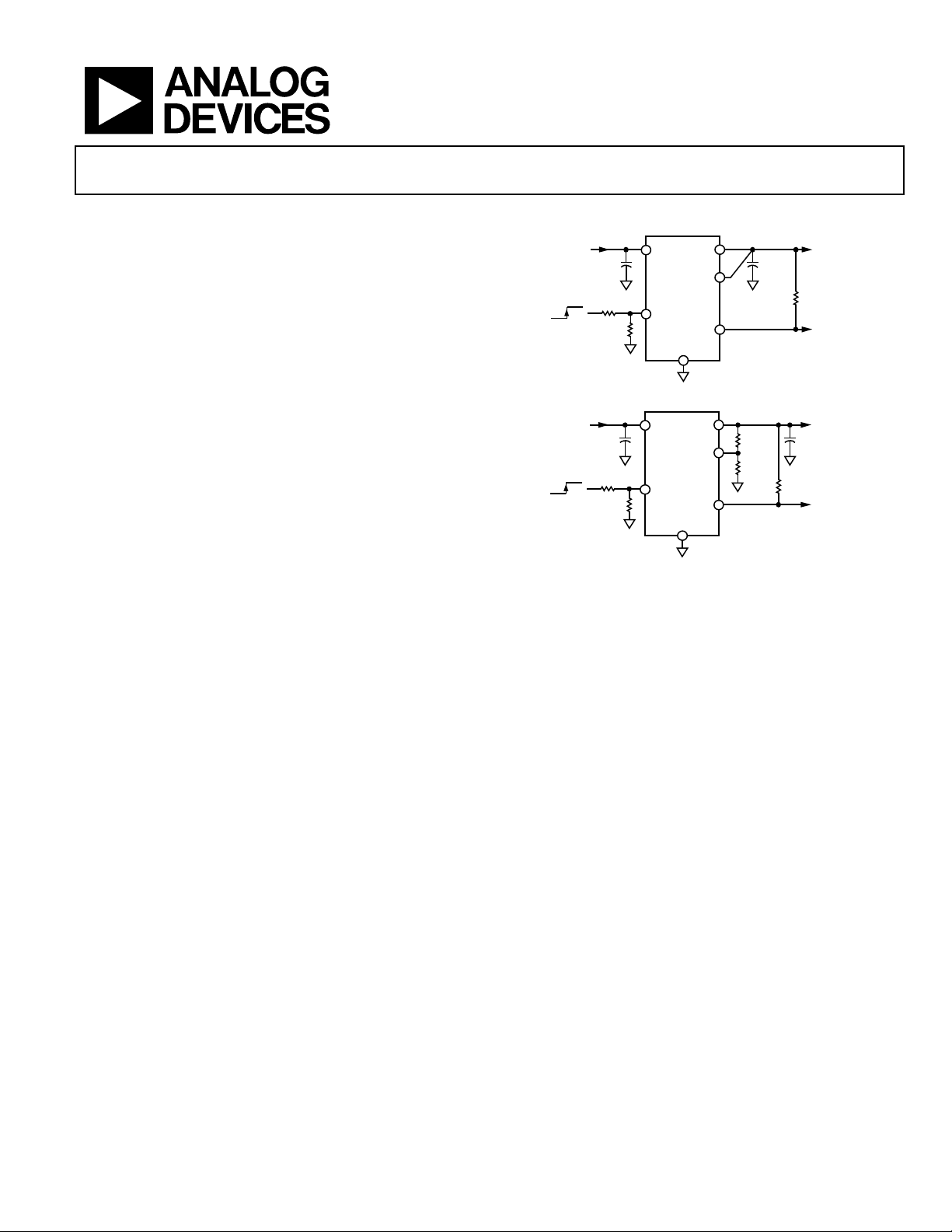
VOUT = 5V
VIN = 8V
PG
VOUTVIN
PG
GND
SENSE
EN/
UVLO
RPG
100kΩ
R2
100kΩ
R1
100kΩ
COUT
1µF
CIN
1µF
ON
OFF
+
+
09506-001
VOUT = 5V
VIN = 8V
PG
VOUTVIN
PG
GND
ADJ
EN/
UVLO
RPG
100kΩ
R4
100kΩ
R3
100kΩ
COUT
1µF
CIN
1µF
ON
OFF
+
+
R2
13kΩ
R1
40.2kΩ
09506-002
Data Sheet
FEATURES
Input voltage range: 3.3 V to 20 V
Maximum output current: 300 mA
Low noise: 15 µV rms for fixed output versions
PSRR performance of 60 dB at 10 kHz, V
Reverse current protection
Low dropout voltage: 200 mV at 300 mA load
Initial accuracy: ±0.8%
Accuracy over line, load, and temperature: −2%, +1%
Low quiescent current (V
= 5 V), I
IN
GND
load
Low shutdown current: 40 µA at V
IN
Stable with small 1 µF ceramic output capacitor
7 fixed output voltage options: 1.5 V, 1.8 V, 2.5 V, 3 V, 3.3 V,
5 V, and 9 V
Adjustable output from 1.22 V to V
Foldback current limit and thermal overload protection
User programmable precision UVLO/enable
Power good indicator
8-lead LFCSP and 8-lead SOIC packages
= 3.3 V
OUT
= 750 μA with 300 mA
= 12 V
– VDO
IN
TYPICAL APPLICATION CIRCUITS
Figure 1. ADP7102 with Fixed Output Voltage, 5 V
Figure 2. ADP7102 with Adjustable Output Voltage, 5 V
APPLICATIONS
Regulation to noise sensitive applications: ADC, DAC
circuits, precision amplifiers, high frequency oscillators,
clocks, and PLLs
Communications and infrastructure
Medical and healthcare
Industrial and instrumentation
GENERAL DESCRIPTION
The ADP7102 is a CMOS, low dropout linear regulator that
operates from 3.3 V to 20 V and provides up to 300 mA of
output current. This high input voltage LDO is ideal for
regulation of high performance analog and mixed signal
circuits operating from 19 V to 1.22 V rails. Using an
advanced proprietary architecture, it provides high power
supply rejection, low noise, and achieves excellent line and
load transient response with just a small 1 µF ceramic
output capacitor.
The ADP7102 is available in 7 fixed output voltage options and
an adjustable version, which allows output voltages that range
from 1.22 V to V
− VDO via an external feedback divider.
IN
The ADP7102 output noise voltage is 15 μV rms and is independent of the output voltage. A digital power good output
allows power system monitors to check the health of the output
voltage. A user programmable precision undervoltage lockout
function facilitates sequencing of multiple power supplies.
The ADP7102 is available in 8-lead, 3 mm × 3 mm LFCSP
and 8-lead SOIC packages. The LFCSP offers a very compact
solution and also provides excellent thermal performance for
applications requiring up to 300 mA of output current in a
small, low-profile footprint.
Information furnishe d by Analog Devices is believed to be accurate and reliable. However, no
responsibility is assumed by Analog Devices for its use, nor for any infringements of patents or other
rights of third parties that may result from its use. Specifications subject to change without notice. No
license is granted by implication or otherwise under any patent or patent rights of Analog Devices.
One Technology Way, P.O. Box 9106, Norwood, MA 02062-9106, U.S.A.
Tel: 781.329.4700
www.analog.com

ADP7102 Data Sheet
TABLE OF CONTENTS
Features .............................................................................................. 1
Applications ....................................................................................... 1
Typical Application Circuits ............................................................ 1
General Description ......................................................................... 1
Revision History ............................................................................... 2
Specifications ..................................................................................... 3
Input and Output Capacitor, Recommended Specifications .. 4
Absolute Maximum Ratings ............................................................ 5
Thermal Data ................................................................................ 5
ESD Caution .................................................................................. 5
Pin Configurations and Function Descriptions ........................... 6
Typical Performance Characteristics ............................................. 7
REVISION HISTORY
11/11—Rev. 0 to Rev. A
Changes to Figure 50 ...................................................................... 14
10/11—Revision 0: Initial Version
Theory of Operation ...................................................................... 17
Applications Information .............................................................. 18
Capacitor Selection .................................................................... 18
Programable Undervoltage Lockout (UVLO) ........................... 19
Power Good Feature .................................................................. 20
Noise Reduction of the Adjustable ADP7102 ........................ 20
Current Limit and Thermal Overload Protection ................. 21
Thermal Considerations ............................................................ 21
Printed Circuit Board Layout Considerations ............................ 24
Outline Dimensions ....................................................................... 25
Ordering Guide .......................................................................... 26
Rev. A | Page 2 of 28
Data Sheet ADP7102
I
= 300 mA, VIN = 10 V, TJ = −40°C to +125°C
1400
µA
SPECIFICATIONS
VIN = (V
Table 1.
Parameter Symbol Conditions Min Typ Max Unit
INPUT VOLTAGE RANGE VIN 3.3 20 V
OPERATING SUPPLY CURRENT I
I
I
I
I
I
I
SHUTDOWN CURRENT I
EN = GND, VIN = 12 V, TJ = −40°C to +125°C 75 µA
INPUT REVERSE CURRENT I
EN = GND, VIN = 0 V, V
OUTPUT VOLTAGE ACCURACY
Fixed Output Voltage Accuracy V
1 mA < I
Adjustable Output Voltage
1 mA < I
LINE REGULATION ∆V
LOAD REGULATION1 ∆V
I
ADJ INPUT BIAS CURRENT ADJ
SENSE INPUT BIAS CURRENT SENSE
DROPOUT VOLTAGE2 V
I
I
I
I
I
START-UP TIME3 t
CURRENT-LIMIT THRESHOLD4 I
PG OUTPUT LOGIC LEVEL
PG Output Logic High PG
PG Output Logic Low PG
PG OUTPUT THRESHOLD
Output Voltage Falling PG
Output Voltage Rising PG
THERMAL SHUTDOWN
Thermal Shutdown Threshold TSSD TJ rising 150
Thermal Shutdown Hysteresis TS
+ 1 V) or 3.3 V (whichever is greater), EN = VIN, I
OUT
I
GND
EN = GND, VIN = 12 V 40 µA
GND-SD
EN = GND, VIN = 0 V, V
REV-INPUT
I
OUT
V
I
ADJ
Accuracy
/∆VIN VIN = (V
OUT
/∆I
OUT
OUT
1 mA < I
I-BIAS
I-BIAS
I
DROPOUT
V
STA RT-UP
450 575 750 mA
LIMIT
IOH < 1 µA 1.0 V
HIGH
IOL < 2 mA 0.4 V
LOW
−9.2 %
FAL L
−6.5 %
RISE
15
SD-HYS
= 10 mA, CIN = C
OUT
= 100 µA, VIN = 10 V 400 µA
OUT
= 100 µA, VIN = 10 V, TJ = −40°C to +125°C 900 µA
OUT
= 10 mA, VIN = 10 V 450 µA
OUT
= 10 mA, VIN = 10 V, TJ = −40°C to +125°C 1050 µA
OUT
= 150 mA, VIN = 10 V 650 µA
OUT
= 150 mA, VIN = 10 V, TJ = −40°C to +125°C 1250 µA
OUT
= 300 mA, VIN = 10 V 750 µA
OUT
OUT
= 20 V 0.3 µA
OUT
= 20 V, TJ = −40°C to +125°C 5 µA
OUT
= 10 mA –0.8 +0.8 %
OUT
< 300 mA, VIN = (V
T
T
I
OUT
= −40°C to +125°C
J
= 10 mA 1.21 1.22 1.23 V
OUT
< 300 mA, VIN = (V
OUT
= −40°C to +125°C
J
+ 1 V ) to 20 V, TJ = −40°C to +125°C −0.015 +0.015 %/V
OUT
= 1 mA to 300 mA 0.2 %/A
OUT
= 1 mA to 300 mA, TJ = −40°C to +125°C 1.0 %/A
OUT
< 300 mA, VIN = (V
OUT
= 1 µ F, TA = 25°C, unless otherwise noted.
OUT
+ 1 V) to 20 V,
OUT
+ 1 V) to 20 V,
OUT
+ 1 V) to 20 V,
OUT
–2 +1 %
1.196 1.232 V
10 nA
ADJ connected to VOUT
1 mA < I
SENSE connected to VOUT, V
OUT
OUT
OUT
OUT
OUT
OUT
OUT
< 300 mA, VIN = (V
OUT
+ 1 V) to 20 V,
OUT
= 1.5 V
OUT
1 μA
= 10 mA 20 mV
= 10 mA, TJ = −40°C to +125°C 40 mV
= 150 mA 100 mV
= 150 mA, TJ = −40°C to +125°C 175 mV
= 300 mA 200 mV
= 300 mA, TJ = −40°C to +125°C 325 mV
= 5 V 800 µs
°C
°C
Rev. A | Page 3 of 28
ADP7102 Data Sheet
Start Threshold
V
TJ = −40°C to +125°C
3.2
V
Parameter Symbol Conditions Min Typ Max Unit
PROGRAMMABLE EN/UVLO
UVLO Threshold rising UVLO
UVLO Threshold falling UVLO
UVLO Hysteresis Current UVLO
Enable Pulldown Current I
INPUT VOLTAGE
Shutdown Threshold V
Hysteresis 250 mV
OUTPUT NOISE OUT
10 Hz to 100 kHz, VIN = 6.3 V, V
10 Hz to 100 kHz, VIN = 8 V, V
10 Hz to 100 kHz, VIN = 12 V, V
10 Hz to 100 kHz, VIN = 5.5 V, V
10 Hz to 100 kHz, VIN = 12 V, V
10 Hz to 100 kHz, VIN = 18 V, V
POWER SUPPLY REJECTION RATIO PSRR 100 kHz, VIN = 4.3 V, V
100 kHz, VIN = 6 V, V
10 kHz, VIN = 4.3 V, V
10 kHz, VIN = 6 V, V
100 kHz, VIN = 3.3 V, V
100 kHz, VIN = 6 V, V
100 kHz, VIN = 16 V, V
10 kHz, VIN = 3.3 V, V
10 kHz, VIN = 6 V, V
10 kHz, VIN = 16 V, V
1
Based on an end-point calculation using 1 mA and 300 mA loads. See Figure 6 for typical load re gulation performance for loads less than 1 mA.
2
Dropout voltage is defined as the input-to-output voltage differential when the input voltage is set to the nominal output voltage. This applies only for output
voltages above 3.0 V.
3
Start-up time is defined as the time between the rising edge of EN to VOUT being at 90% of its nominal value.
4
Current-limit threshold is defined as the current at which the output voltage drops to 90% of the specified typical value. For example, the current limit for a 5.0 V
output voltage is defined as the current that causes the output voltage to drop to 90% of 5.0 V, or 4.5 V.
3.3 V ≤ VIN ≤ 20 V, TJ = −40°C to +125°C 1.18 1.23 1.28 V
RISE
3.3 V ≤ VIN ≤ 20 V, TJ = −40°C to +125°C, 10 kΩ
FAL L
1.13 V
in series with enable pin
VEN > 1.25 V, TJ = −40°C to +125°C 7.5 9.8 12 µA
HYS
EN = VIN 500 nA
EN-IN
STA RT
TJ = −40°C to +125°C 2.45 V
SHUTDOWN
10 Hz to 100 kHz, VIN = 5.5 V, V
NOISE
= 1.8 V 15 µV rms
OUT
= 3.3 V 15 µV rms
OUT
= 5 V 15 µV rms
OUT
= 9 V 15 µV rms
OUT
= 1.5 V,
OUT
18 µV rms
adjustable mode
OUT
= 5 V,
30 µV rms
adjustable mode
= 15 V,
OUT
65 µV rms
adjustable mode
= 3.3 V 50 dB
OUT
= 5 V 50 dB
OUT
= 3.3 V 60 dB
OUT
= 5 V 60 dB
OUT
= 1.8 V, adjustable mode 50 dB
OUT
= 5 V, adjustable mode 60 dB
OUT
= 15 V, adjustable mode 60 dB
OUT
= 1.8 V, adjustable mode 60 dB
OUT
= 5 V, adjustable mode 80 dB
OUT
= 15 V, adjustable mode 80 dB
OUT
INPUT AND OUTPUT CAPACITOR, RECOMMENDED SPECIFICATIONS
Table 2.
Parameter Symbol Conditions Min Typ Max Unit
Minimum Input and Output Capacitance1 C
Capacitor ESR R
1
The minimum input and output capacitance should be greater than 0.7 μF over the full range of operating conditions. The full range of operating conditions in the
application must be considered during device selection to ensure that the minimum capacitance specification is met. X7R and X5R type capacitors are recommended;
Y5V and Z5U capacitors are not recommended for use with any LDO.
TA = −40°C to +125°C 0.7 µF
MIN
TA = −40°C to +125°C 0.001 0.2 Ω
ESR
Rev. A | Page 4 of 28
Data Sheet ADP7102
Operating Ambient Temperature Range
–40°C to +85°C
ABSOLUTE MAXIMUM RATINGS
Table 3.
Parameter Rating
VIN to GND –0.3 V to +22 V
VOUT to GND –0.3 V to +20 V
EN/UVLO to GND –0.3 V to VIN
PG to GND –0.3 V to VIN
SENSE/ADJ to GND –0.3 V to VOUT
Storage Temperature Range –65°C to +150°C
Operating Junction Temperature Range –40°C to +125°C
Soldering Conditions JEDEC J-STD-020
Stresses above those listed under absolute maximum ratings
may cause permanent damage to the device. This is a stress
rating only and functional operation of the device at these or
any other conditions above those indicated in the operational
section of this specification is not implied. Exposure to absolute
maximum rating conditions for extended periods may affect
device reliability.
THERMAL DATA
Absolute maximum ratings apply individually only, not in
combination. The ADP7102 can be damaged when the junction
temperature limit is exceeded. Monitoring ambient temperature
does not guarantee that T
limits. In applications with high power dissipation and poor
thermal resistance, the maximum ambient temperature may
have to be derated.
In applications with moderate power dissipation and low PCB
thermal resistance, the maximum ambient temperature can
exceed the maximum limit as long as the junction temperature
is within specification limits. The junction temperature (T
the device is dependent on the ambient temperature (T
power dissipation of the device (P
ambient thermal resistance of the package (θ
Maximum junction temperature (T
ambient temperature (T
formula
T
= TA + (PD × θJA)
J
Junction-to-ambient thermal resistance (θ
based on modeling and calculation using a 4-layer board. The
junction-to-ambient thermal resistance is highly dependent on
the application and board layout. In applications where high
maximum power dissipation exists, close attention to thermal
is within the specified temperature
J
) of
J
), the
A
), and the junction-to-
D
).
JA
) is calculated from the
J
) and power dissipation (PD) using the
A
) of the package is
JA
board design is required. The value of θ
on PCB material, layout, and environmental conditions. The
specified values of θ
are based on a 4-laye r, 4 in. × 3 in. circuit
JA
board. See JESD51-7 and JESD51-9 for detailed information on
the board construction. For additional information, see the
AN-617 Application Note, MicroCSP™ Wafer Level Chip Scale
Package, available at www.analog.com.
Ψ
is the junction-to-board thermal characterization parameter
JB
with units of °C/W. The package’s Ψ
calculation using a 4-layer board. The JESD51-12, Guidelines
for Reporting and Using Electronic Package Thermal
Information, states that thermal characterization parameters are
not the same as thermal resistances. Ψ
component power flowing through multiple thermal paths
rather than a single path as in thermal resistance, θ
Ψ
thermal paths include convection from the top of the
JB
package as well as radiation from the package, factors that make
Ψ
more useful in real-world applications. Maximum junction
JB
temperature (T
and power dissipation (P
T
= TB + (PD × ΨJB)
J
) is calculated from the board temperature (TB)
J
) using the formula
D
See JESD51-8 and JESD51-12 for more detailed information
about Ψ
.
JB
Thermal Resistance
θJA and ΨJB are specified for the worst-case conditions, that is, a
device soldered in a circuit board for surface-mount packages.
θ
is a parameter for surface-mount packages with top
JC
mounted heatsinks. θ
is presented here for reference on l y.
JC
Table 4. Thermal Resistance
Package Type
θJA θJC
8-Lead LFCSP 40.1 27.1 17.2 °C/W
8-Lead SOIC 48.5 58.4 31.3 °C/W
ESD CAUTION
may vary, depending
JA
is based on modeling and
JB
measures the
JB
. Therefore,
JB
ΨJB Unit
Rev. A | Page 5 of 28
ADP7102 Data Sheet
NOTES
1. NC = NO CONNECT. DO NOT CONNECT TO
THIS PIN.
2. IT IS HI GHLY RECOM M E NDE D THAT THE
EXPOSED PAD ON THE BOTTOM OF THE
PACKAGE BE CONNE CTED TO THE GROUND
PLANE ON T HE BOARD.
3GND
4NC
1VOUT
2SENSE/ADJ
6 GND
5 EN/UVLO
8 VIN
7 PG
ADP7102
TOP VIEW
(Not to S cale)
09506-003
NOTES
1. NC = NO CONNECT. DO NOT CONNECT TO
THIS PIN.
2. IT IS HI GHLY RECOM M E NDE D THAT THE
EXPOSED PAD ON THE BOTTOM OF THE
PACKAGE BE CONNE CTED TO THE GROUND
PLANE ON T HE BOARD.
VOUT
1
SENSE/ADJ
2
GND
3
NC
4
VIN
8
PG
7
GND
6
EN/UVLO
5
ADP7102
TOP VIEW
(Not to S cale)
09506-104
Sense (SENSE). Measures the actual output voltage at the load and feeds it to the error amplifier.
performance and is electrically connected to GND inside the package. It is highly recommended
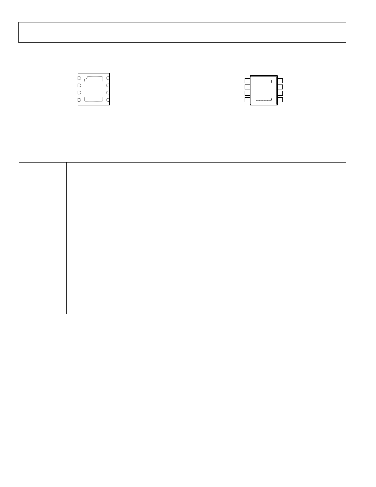
PIN CONFIGURATIONS AND FUNCTION DESCRIPTIONS
Figure 3. LFCSP Package
Figure 4. Narrow Body SOIC Package
Table 5. Pin Function Descriptions
Pin No. Mnemonic Description
1 VOUT Regulated Output Voltage. Bypass VOUT to GND with a 1 µF or greater capacitor.
2 SENSE/ADJ
Connect SENSE as close as possible to the load to minimize the effect of IR drop between the
regulator output and the load. This function applies to fixed voltages only.
Adjust Input (ADJ). An external resistor divider sets the output voltage. This function applies to
adjustable voltages only.
3 GND Ground.
4 NC Do Not Connect to this Pin.
5 EN/UVLO Enable Input (EN). Drive EN high to turn on the regulator; drive EN low to turn off the regulator.
For automatic startup, connect EN to VIN.
Programmable Undervoltage Lockout (UVLO). When the programmable UVLO function is used,
the upper and lower thresholds are determined by the programming resistors.
6 GND Ground.
7 PG Power Good. This open-drain output requires an external pull-up resistor to VIN or VOUT. If the
part is in shutdown, current limit, thermal shutdown, or falls below 90% of the nominal output
voltage, PG immediately transitions low. If the power good function is not used, the pin may be
left open or connected to ground.
8 VIN Regulator Input Supply. Bypass VIN to GND with a 1 µF or greater capacitor.
EPAD Exposed Pad. Exposed paddle on the bottom of the package. The EPAD enhances thermal
that the EPAD be connected to the ground plane on the board.
Rev. A | Page 6 of 28
Data Sheet ADP7102
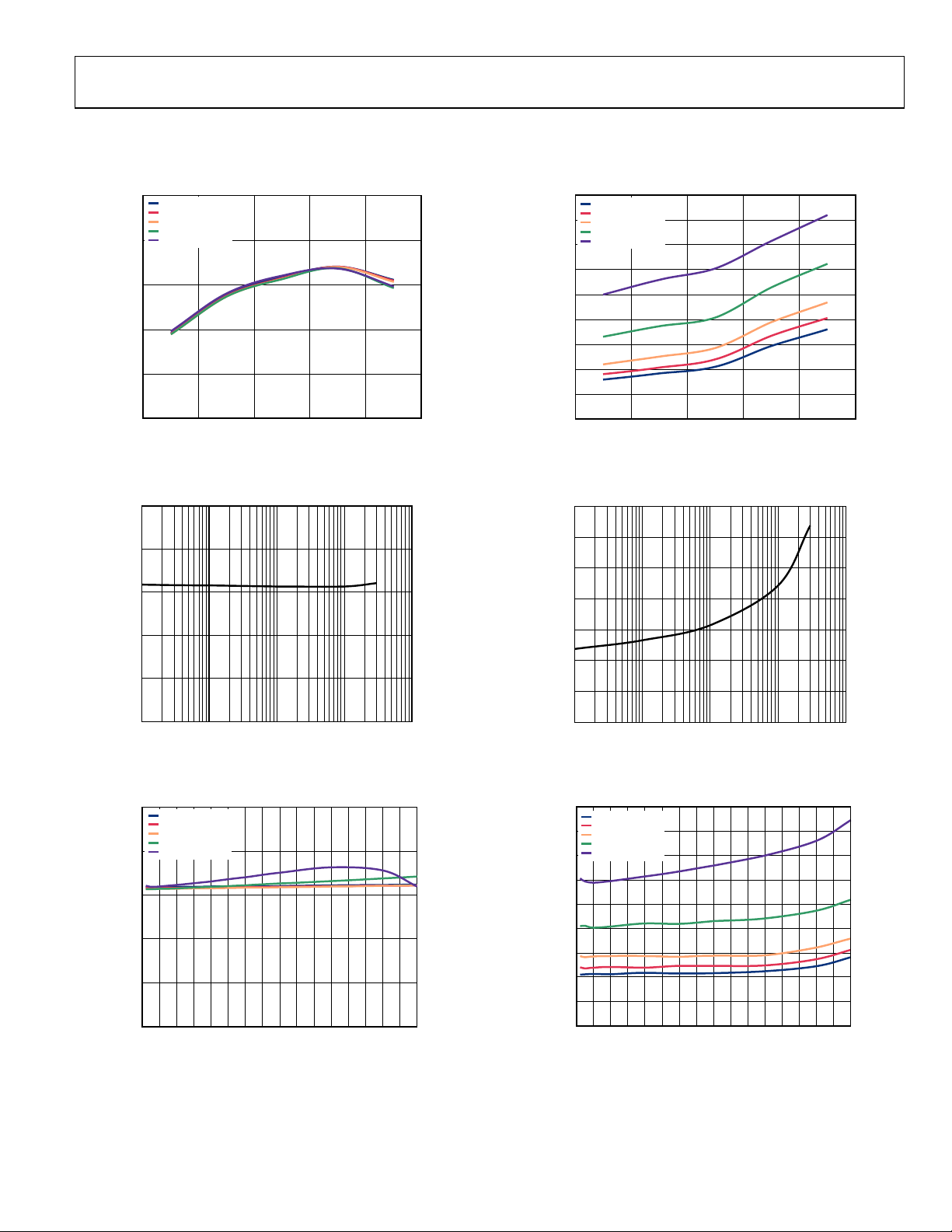
3.25
3.27
3.29
3.31
3.33
3.35
V
OUT
(V)
–40°C –5°C 25°C 85°C 125°C
TJ (°C)
LOAD = 100µA
LOAD = 1mA
LOAD = 10mA
LOAD = 100mA
LOAD = 300mA
09506-004
3.25
3.27
3.29
3.31
3.33
3.35
0.1 1 10 100 1000
V
OUT
(V)
I
LOAD
(mA)
09506-005
3.25
3.27
3.29
3.31
3.33
3.35
4 6 8 10 12 14 16 18 20
V
OUT
(V)
VIN (V)
LOAD = 100µA
LOAD = 1mA
LOAD = 10mA
LOAD = 100mA
LOAD = 300mA
09506-006
0
100
200
300
400
500
600
700
800
900
GROUND CURRENT (µA)
–40°C –5°C 25°C 85°C 125°C
TJ(°C)
LOAD = 100µA
LOAD = 1mA
LOAD = 10mA
LOAD = 100mA
LOAD = 300mA
09506-007
0
100
200
300
400
500
600
700
0.1 1 10 100 1000
GROUND CURRENT (µA)
I
LOAD
(mA)
09506-008
0
100
200
300
400
500
600
700
800
90
0
64 8 10 12 14 16 18 20
GROUND CURRENT (µA)
V
IN
(V)
LOAD = 100µA
LOAD = 1mA
LOAD = 10mA
LOAD = 100mA
LOAD = 300mA
09506-009
TYPICAL PERFORMANCE CHARACTERISTICS
VIN = 5 V, V
= 3.3 V, I
OUT
= 1 mA, CIN = C
OUT
= 1 µF, TA = 25°C, unless otherwise noted.
OUT
Figure 5. Output Voltage vs. Junction Temperature
Figure 6. Output Voltage vs. Load Current
Figure 8. Ground Current vs. Junction Temperature
Figure 9. Ground Current vs. Load Current
Figure 7. Output Voltage vs. Input Voltage
Figure 10. Ground Current vs. Input Voltage
Rev. A | Page 7 of 28
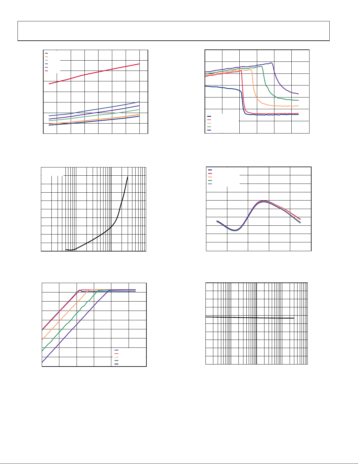
ADP7102 Data Sheet
0
20
40
60
80
100
120
140
160
–50 –25 0 25 50 75 100 125
SHUTDOWN CURRE NT (µA)
TEMPERATURE (°C)
3.3V
4.0V
6.0V
8.0V
12.0V
20.0V
09506-010
0
20
40
60
80
100
120
140
160
180
200
1 10 100 1000
DROPOUT ( mV )
I
LOAD
(mA)
V
OUT
= 3.3V
T
A
= 25°C
09506-011
2.90
2.95
3.00
3.05
3.10
3.15
3.20
3.25
3.30
3.35
3.10 3.20 3.30 3.40 3.50 3.60 3.70
V
OUT
(V)
VIN (V)
09506-012
LOAD = 100µA
LOAD = 1mA
LOAD = 10mA
LOAD = 100mA
LOAD = 300mA
0
200
400
600
800
1000
1200
1400
3.10 3.20 3.30 3.40 3.50 3.60 3.70
GROUND CURRENT (µA)
VIN (V)
09506-013
LOAD = 5mA
LOAD = 10mA
LOAD = 100mA
LOAD = 200mA
LOAD = 300mA
4.95
4.96
4.97
4.98
4.99
5.00
5.01
5.02
5.03
5.04
5.05
V
OUT
(V)
–40°C –5°C 25°C 85°C 125°C
T
J
(
°C
)
LOAD = 100µA
LOAD = 1mA
LOAD = 10mA
LOAD = 100mA
LOAD = 300mA
09506-014
4.95
4.96
4.97
4.98
4.99
5.00
5.01
5.02
5.03
5.04
5.05
0.1 1 10 100 1000
V
OUT
(V)
I
LOAD
(mA)
09506-015
Figure 11. Shutdown Current vs. Temperature at Various Input Voltages
Figure 12. Dropout Voltage vs. Load Current
Figure 14. Ground Current vs. Input Voltage (in Dropout)
Figure 15. Output Voltage vs. Junction Temperature, V
OUT
= 5 V
Figure 13. Output Voltage vs. Input Voltage (in Dropout)
Figure 16. Output Voltage vs. Load Current, V
OUT
= 5 V
Rev. A | Page 8 of 28
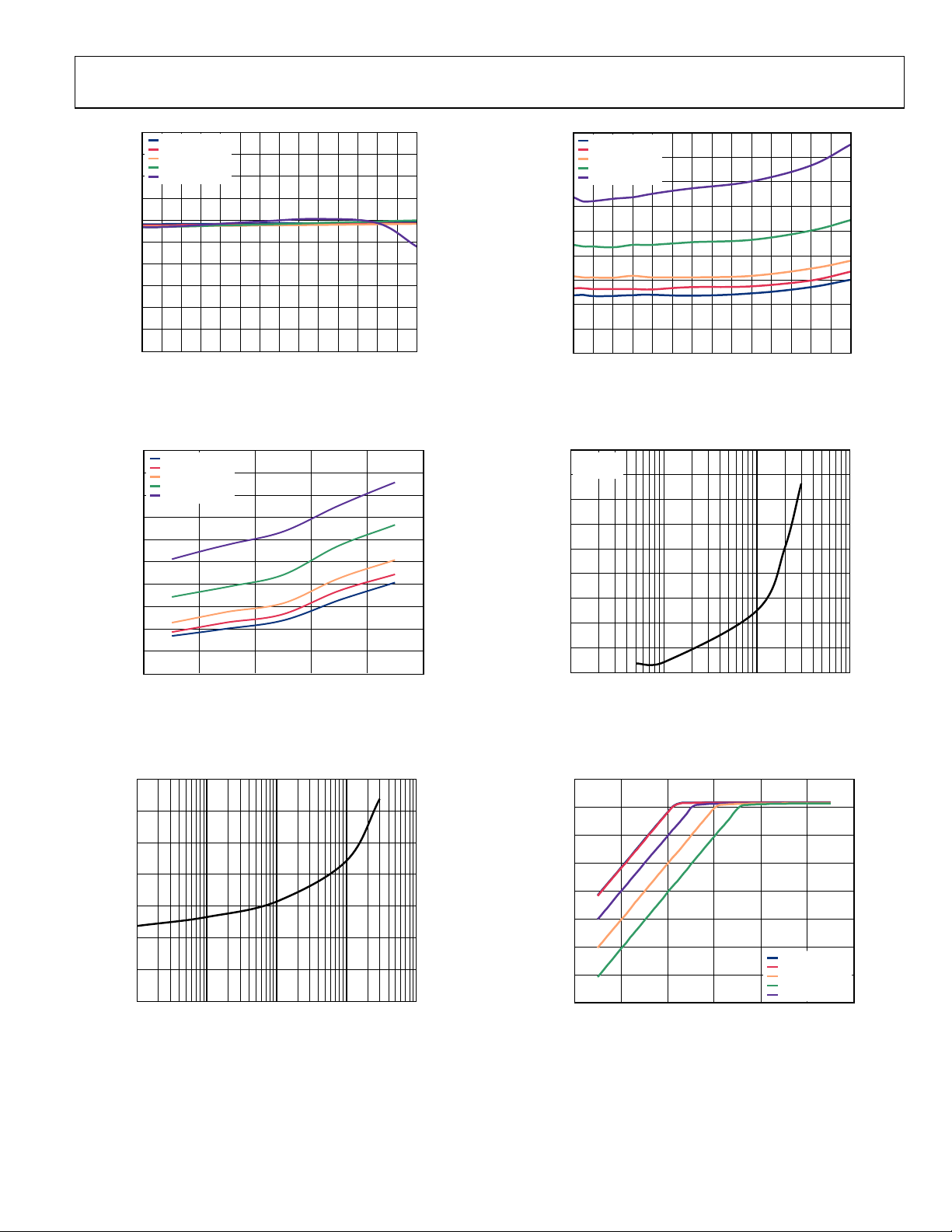
Data Sheet ADP7102
4.95
4.96
4.97
4.98
4.99
5.00
5.01
5.02
5.03
5.04
5.05
6 8 10 12 14 16 18 20
V
OUT
(V)
V
IN
(V)
LOAD = 100µA
LOAD = 1mA
LOAD = 10mA
LOAD = 100mA
LOAD = 300mA
09506-016
09506-118
GROUND CURRENT (µA)
0
100
200
300
400
500
600
700
800
900
1000
–40°C –5°C 25°C 85°C 125°C
TJ (
°C
)
LOAD = 100µA
LOAD = 1mA
LOAD = 10mA
LOAD = 100mA
LOAD = 300mA
0
100
200
300
400
500
600
700
0.1 1 10 100 1000
GROUND CURRENT (µA)
I
LOAD
(mA)
09506-119
0
100
200
300
400
500
600
700
800
900
GROUND CURRENT (µA)
6 8 10 12 14 16 18 20
VIN (V)
LOAD = 100µA
LOAD = 1mA
LOAD = 10mA
LOAD = 100mA
LOAD = 300mA
09506-120
0
20
40
60
80
100
120
140
160
180
1 10 100 1000
DROPOUT ( mV )
I
LOAD
(mA)
V
OUT
= 5V
T
A
= 25°C
09506-017
4.65
4.70
4.75
4.80
4.85
4.90
4.95
5.00
5.05
4.8 4.9 5.0 5.1 5.2 5.3 5.4
V
OUT
(V)
VIN (V)
09506-018
LOAD = 5mA
LOAD = 10mA
LOAD = 100mA
LOAD = 200mA
LOAD = 300mA
Figure 17. Output Voltage vs. Input Voltage, V
OUT
Figure 18. Ground Current vs. Junction Temperature, V
= 5 V
OUT
= 5 V
Figure 20. Ground Current vs. Input Voltage, V
OUT
= 5 V
Figure 21. Dropout Voltage vs. Load Current, V
OUT
= 5 V
Figure 19. Ground Current vs. Load Current, V
OUT
= 5 V
Figure 22. Output Voltage vs. Input Voltage (in Dropout), V
OUT
= 5 V
Rev. A | Page 9 of 28
 Loading...