QWERTY Keypad Controller
ADP5588
C8C9C8
C9
18
17
19
21
23
22
20
24
CONTROL
REGISTERS
CONTROL
INTERFACE
REF
VOLTAGE
REF
VOLTAGE
R7R6R5R4R3R2R1R0C0C1C2C3C4C5C6
C7
C9
C8
GND
V
CC
SCL
SDA
RST
INT
3 4 5 6 7 8 9 10 11 12 13 14 15 161 2
07673-001
ADP5588
Rev. C
Trademarks and registered trademarks are the property of their respective owners.
Fax: 781.461.3113 ©2008–2012 Analog Devices, Inc. All rights reserved.
Data Sheet
FEATURES
18-GPIO port expander or 10 × 8 keypad matrix
GPIOs configurable to GPIs, GPOs, and keypad rows or
columns
Dual light sensor inputs (C8 and C9)
2
I
C interface
2
I
C register read autoincrement
1.8 V to 3.0 V operation
Keypad lock capability
Open-drain interrupt output
Key press and key release interrupts
GPI interrupt with level programmability
Programmable pull-ups
Key event counter with overflow interrupt
50 μs debounce on the reset line and GPIs
1 μA typical idle current, 55 μA typical polling current drain
for one key press
Small 4 mm × 4 mm LFCSP package
Mobile I/O Expander and
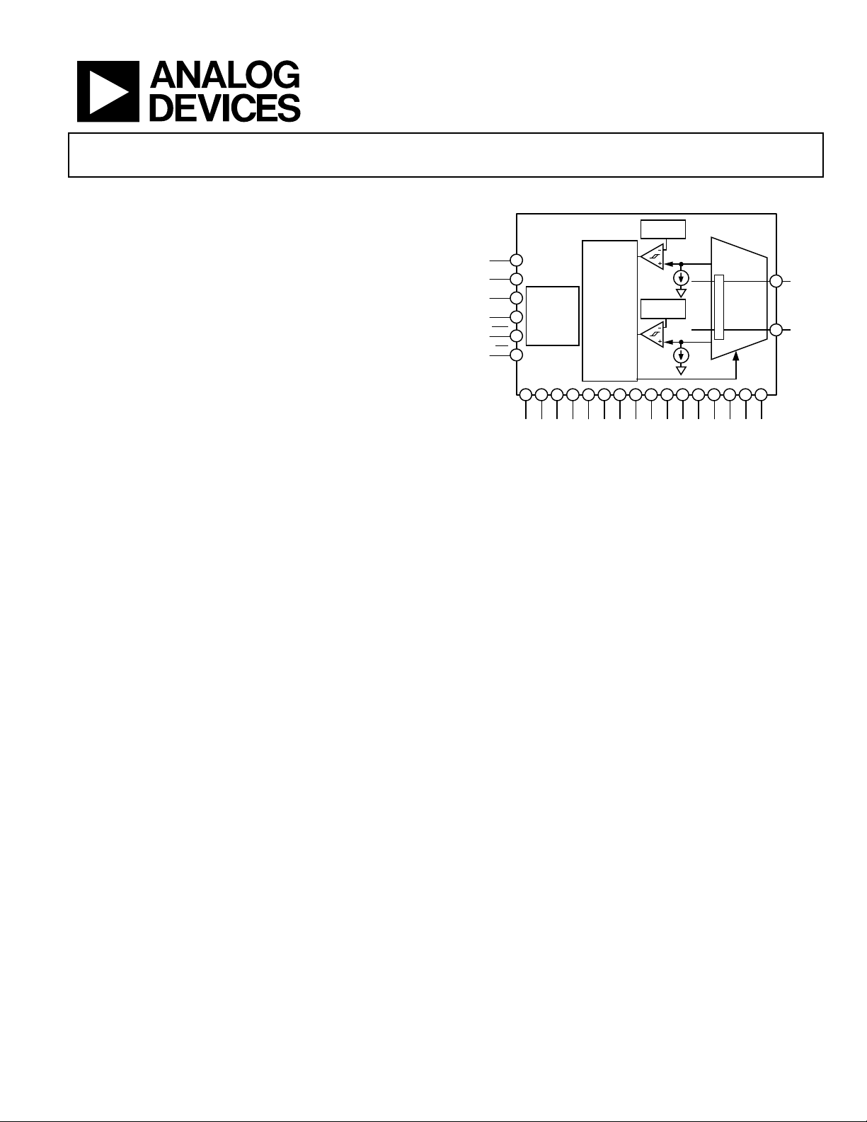
FUNCTIONAL BLOCK DIAGRAM
Figure 1.
APPLICATIONS
Keypad and I/O expander designed for QWERTY type phones
that require a large keypad matrix
GENERAL DESCRIPTION
The ADP5588 is an I/O port expander and keypad matrix
designed for QWERTY type phones that require a large keypad
matrix and expanded I/O lines. I/O expander ICs are used in
mobile platforms as a solution to the limited number of GPIOs
available in the main processor.
In its small 4 mm × 4 mm package, the ADP5588 contains
enough power to handle all key scanning and decoding and flag
the processor of key presses and releases via the I
and interrupt. It frees the main microprocessor from having to
monitor the keypad, thereby minimizing current drain and
increasing processor bandwidth. It is also equipped with a
buffer/FIFO and key event counter to handle and keep track of
up to 10 unprocessed key or GPI events with overflow wrap and
interrupt capability.
The ADP5588 has a keylock capability with an option to trigger
or not trigger an interrupt at key presses and releases. All communication to the main processor is done using one interrupt line
and two I
configured to have a keypad matrix of up to 8 rows × 10 columns
(a maximum of 80 keys).
Information furnishe d by Analog Devices is believed to be accurate and reliable. However, no
responsibility is assumed by Analog Devices for its use, nor for any infringements of patents or other
rights of third parties that may result from its use. Specifications subject to change without notice. No
license is granted by implication or otherwise under any patent or patent rights of Analog Devices.
2
C-compatible interface lines. The ADP5588 can be
2
C® interface
When used for smaller keypad matrices, unused row and
column pins can be reconfigured to act as general-purpose
inputs, outputs, or light sensor inputs. R0, R1, R2, R3, R4, R5,
R6, and R7 denote the row pins of the matrix, while C0, C1, C2,
C3, C4, C5, C6, C7, C8, and C9 denote the column pins. At
power-up, all rows and columns default as GPIs and must be
programmed to function as part of the keypad matrix, GPOs, or
light sensor inputs. In addition to keypad and GPIO functionalities,
C8 and C9 can also be configured as light sensor inputs.
When configured as keypad lines, the function of the C8 and
C9 lines is straightforward: the control interface disconnects
these lines from the comparator inputs, disables the light sensor
comparator, and connects them to the keypad columns of the
keypad matrix. When used as light sensor comparator inputs,
the control interface disconnects these pins from the keypad,
enables the comparators, and connects these lines to the comparator inputs. Two external capacitors (0.1 μF) are required
when these pins are configured as light sensor inputs. When
used as GPIOs, these pins are removed from the keypad and the
light sensor interface, and the light sensor comparators are
disabled, along with the logic for the sensors.
One Technology Way, P.O. Box 9106, Norwood, MA 02062-9106, U.S.A.
Tel: 781.329.4700
www.analog.com

ADP5588 Data Sheet
TABLE OF CONTENTS
Features .............................................................................................. 1
Applications ....................................................................................... 1
Functional Block Diagram .............................................................. 1
General Description ......................................................................... 1
Revision History ............................................................................... 2
Specifications ..................................................................................... 3
DC Electrical Characteristics ...................................................... 3
Absolute Maximum Ratings ............................................................ 5
Thermal Resistance ...................................................................... 5
ESD Caution .................................................................................. 5
Pin Configuration and Function Descriptions ............................. 6
Theory of Operation ........................................................................ 7
REVISION HISTORY
2/12—Rev. B to Rev. C
Changes to Table 12 .......................................................................... 8
Changes to Table 27 ........................................................................ 18
4/09—Rev. A to Rev. B
Changes to Title ................................................................................ 1
Changes to Ordering Guide .......................................................... 26
11/08—Rev. Sp0 to Rev. A
Keypad Operation .........................................................................7
General-Purpose Inputs and Outputs ........................................9
I2C Programming and Digital Control ........................................ 14
Registers ....................................................................................... 15
Register Descriptions ................................................................. 16
Comparator Register Descriptions .......................................... 21
Applications Information .............................................................. 24
Applications Overview .............................................................. 24
Keypad Current .......................................................................... 24
Backlight Control Application .................................................. 24
Outline Dimensions ....................................................................... 26
Ordering Guide .......................................................................... 26
Rev. C | Page 2 of 28

Data Sheet ADP5588
SPECIFICATIONS
TA = TJ = −40°C to +85°C, unless otherwise noted.
DC ELECTRICAL CHARACTERISTICS
Table 1. General DC Electrical Characteristics
Parameter Symbol Conditions Min Typ Max Unit
SUPPLY VOLTAGE
VCC Input Voltage Range VCC 1.7 3.0 V
Photosensor Voltage V
Supply Current1 I
PHOTOSENSOR
CC
With One Key Press ICC V
With One Key Press ICC V
With GPI Low (Pull-Up Enabled)2 I
CC
With GPI Low (Pull-Up Disabled) ICC V
With One GPO Active3 I
CC
AMBIENT LIGHT SENSOR (CMP_IN1, CMP_IN2)
Maximum Sensor Range I
Sensor Supply Current (One Comparator Enabled,
0 Minimum Input Current)
Sensor Current (One Comparator Enabled,
Maximum Input Current)
Sensor Current (Both Comparators Enabled,
Minimum Input Current)
Sensor Current (Both Comparators Enabled,
Maximum Input Current)
4
4
4
4
SENSOR
I
CC
I
CC
I
CC
I
CC
OSCILLATOR CURRENT
Oscillator Current (Enabled) ICC V
1
Operating current measured with I/Os defaulting as GPIs with all pull-ups enabled and all inputs open.
2
With one GPI low.
3
Load = 100 k.Ω
4
Photosensor maximum voltage = VCC + 0.2.
Table 2. I/O DC Electrical Characteristics
Parameter Symbol Conditions Min Typ Max Unit
INPUT LOGIC LEVELS (SCL, SDA, RST, C0 to C9, R0 to R7)1
Logic Low Input Voltage VIL 1.7 V ≤ VIO ≤ 3.0 V 0.2 x VCC V
Logic High Input Voltage VIH 1.7 V ≤ VIO ≤ 3.0 V 0.65 x VCC V
Schmitt Trigger Hysteresis V
Input Leakage Current V
HYST
I-LEAKAGE
OUTPUT LOGIC LEVELS (C0 to C9, R0 to R7)
Logic Low Output Voltage VOL I
Output High Voltage VOH I
OUTPUT LOGIC LEVELS (INT, SDA)
Output Low Voltage VOL I
Output High Voltage VOH 1.7 V ≤ VCC ≤ 3.0 V 0.95 × VCC V
Logic High Leakage Current V
PULL-UP RESISTANCE FOR GPIOs (C0 to C9, R0 to R7)2 R
1
Power-up default current. All I/Os default as GPIs and are open; C8 and C9 default as GPIs; I2C is idle.
2
GPIO internal pull-ups are designed to 100 kΩ.
O-LEAKAGE
PULL-UP
VCC + 0.2
V
V
V
V
V
V
V
V
= 1.8 V to 3.0 V, TA = −40°C to +85°C 1 10 A
CC
= 1.8 V, TA = −40°C to +85°C 55 90 A
CC
= 3.0 V, TA = −40°C to +85°C 100 200 A
CC
= 1.8 V to 3.0 V, TA = −40°C to +85°C 20 50 A
CC
= 1.8 V to 3.0 V, TA = −40°C to +85°C 2 10 A
CC
= 1.8 V, TA = −40°C to +85°C 50 A
CC
= 1.8 V to 3.0 V, TA = 25°C 0.85 1.0 1.15 mA
CC
= 1.8 V to 3.0 V 100 150 A
CC
= 1.8 V to 3.0 V 160 200 A
CC
= 1.8 V to 3.0 V 130 180 A
CC
= 1.8 V to 3.0 V 240 400 A
CC
= 1.8 V to 3.0 V 40 A
CC
0.10 V
1.7 V ≤ VIO ≤ 3.0 V −1 1 µA
= 1 mA 0.40 V
SINK
= 1 mA VCC − 0.3 V V
SOURCE
= 3 mA
SINK
1.7 V ≤ V
≤ 3.0 V
CC
0.40 V
1.7 V ≤ VCC ≤ 3.0 V 0.1 1 µA
100 kΩ
Rev. C | Page 3 of 28
ADP5588 Data Sheet
p
p
p
Table 3. Comparator Input Capacitor
Parameter Symbol Min Typ Max Unit
Comparator Input Capacitor Value C
Table 4. Capacitance Loading1
Parameter Symbol Min Typ Max Unit
I/O Input Capacitance C
I/O Output Loading Capacitance C
Capacitive Load for Each Bus Line C
1
Guaranteed by design.
2
CB = total capacitance of one bus line in picofarads.
Table 5. AC Characteristics1
Parameter Symbol Min Typ Max Unit
Delay from Reset Deassertion to I2C Access R
Keypad Unlock Timer T
Keypad Interrupt Mask Timer T
Debounce TD 50 μs
Filter Time T
1
Guaranteed by design.
2
Table 6. I
C AC Electrical Characteristics1
Parameter Symbol Min Typ Max Unit
SCL Clock Frequency f
SCL High Time t
SCL Low Time t
Data Setup Time tSU,
Data Hold Time tHD,
Setup Time for Repeated Start tSU,
Hold Time for Start/Repeated Start tHD,
Bus Free Time for Stop and Start t
Setup Time for Stop Condition tSU,
Rise Time for SCL and SDA2 t
Fall Time for SCL and SDA2 t
Pulse Width of Suppressed Spike tSP 0 50 μs
1
Guaranteed by design.
2
tR and tF are measured between 0.3 × VCC and 0.7 × VCC.
0.1 μF
COMP
IN
OUT
2
B
60 μs
STD
7 sec
KUT
31 sec
KIMT
0.070 12 sec
TTR
400 kHz
SCL
0.6 μs
HIGH
1.3 μs
LOW
100 ns
DAT
0 0.9 μs
DAT
0.6 μs
STA
0.6 μs
STA
1.3 μs
BUF
0.6 μs
STO
20 + 0.1 CB 300 ns
R
20 + 0.1 CB 300 ns
F
1 10
50
400
F
F
F
SDA
t
t
LOW
SCL
S
S = START CONDITION
Sr = REPEATED START CONDITION
P = STOP CO NDITION
t
R
t
HD, DAT
t
SU, DAT
t
HIGH
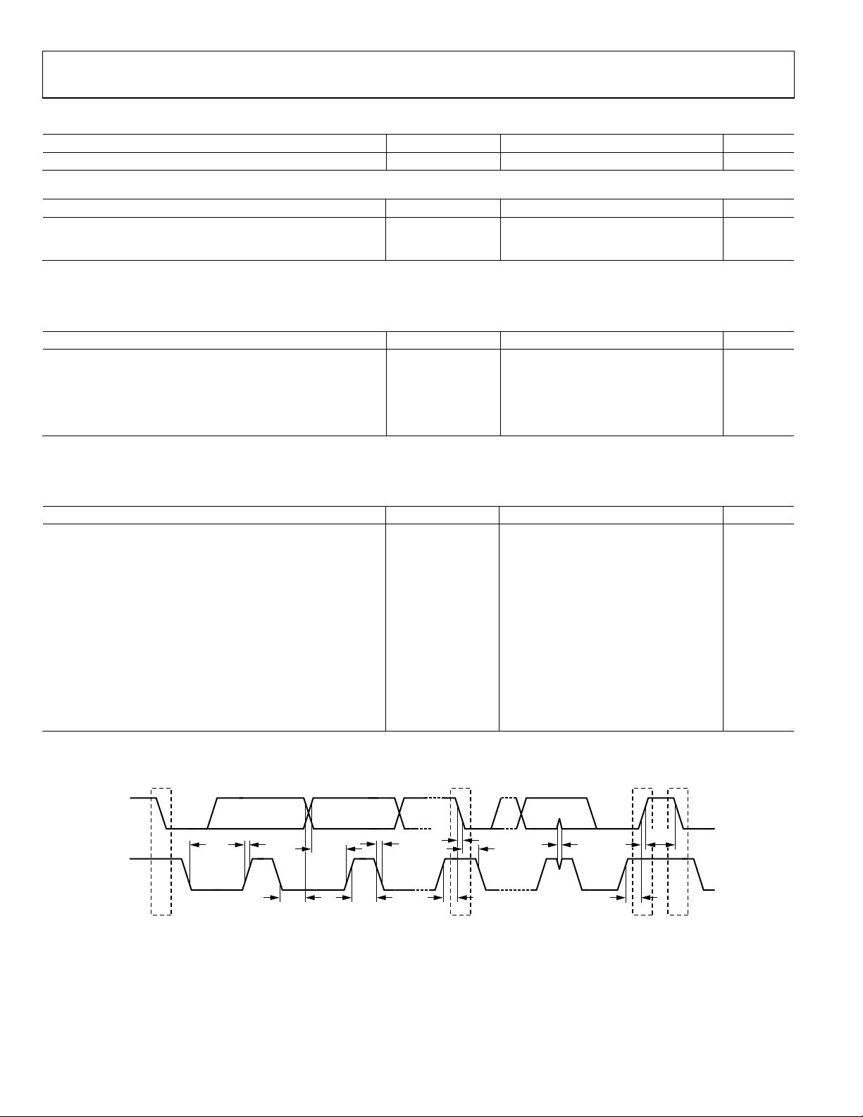
Figure 2. I
t
F
t
F
t
SU, STA
2
C Interface Timing Diagram
Sr P S
t
HD, STA
t
SP
t
SU, STO
BUF
t
R
07673-002
Rev. C | Page 4 of 28

Data Sheet ADP5588
ABSOLUTE MAXIMUM RATINGS
Table 7.
Parameter Rating
VCC −3 V to +4.0 V
R0 to R7, C0 to C9 −3 V to VCC + 0.3 V
SCL −3 V to VCC+ 0.3 V
SDA −3 V to VCC + 0.3 V
−3 V to VCC + 0.3 V
RST
−3 V to VCC + 0.3 V
INT
GND −0.3 V to +0.3 V
Operating Ambient Temperature Range −40°C to +85°C
Operating Junction Temperature Range −40°C to +125°C
Storage Temperature Range −65°C to +150°C
ESD Machine Model ±200 V
ESD Human Body Model ±2000 V
ESD Charged Device Model ±1000 V
Soldering Condition JEDEC J-STD-020
Stresses above those listed under Absolute Maximum Ratings
may cause permanent damage to the device. This is a stress
rating only; functional operation of the device at these or any
other conditions above those indicated in the operational
section of this specification is not implied. Exposure to absolute
maximum rating conditions for extended periods may affect
device reliability.
THERMAL RESISTANCE
θJA is specified for the worst-case conditions, that is, a device
soldered in a circuit board for surface-mount packages.
Table 8. Thermal Resistance
Package Type θJA θJC Unit
24-Lead LFCSP_VQ 57.8 9.4 °C/W
Maximum Power 600 mW
ESD CAUTION
Rev. C | Page 5 of 28

ADP5588 Data Sheet
PIN 1
INDICATOR
NOTES
1. NC = NO CONNECT.
2. EXPOSED PAD MUST BE CONNECTED TO GROUND.
1R7
2R6
3R5
4R4
5R3
6R2
15 C6
16 C7
17 CMP_IN1/C8
18 CMP_IN2/C9
14 C5
13 C4
7
R1
8R0
9C0
11C2
12C3
10C1
21
V
CC
22
SDA
23
SCL
24
INT
20
RST
19
GND
TOP VIEW
(Not to S cale)
ADP5588
07673-003
8
R0
GPIO, Row 0 in the Keypad Matrix.
23
SCL
I2C Clock.
PIN CONFIGURATION AND FUNCTION DESCRIPTIONS
Figure 3. Pin Configuration
Table 9. Pin Function Descriptions
Pin No. Mnemonic Description
1 R7 GPIO, Row 7 in the Keypad Matrix.
2 R6 GPIO, Row 6 in the Keypad Matrix.
3 R5 GPIO, Row 5 in the Keypad Matrix.
4 R4 GPIO, Row 4 in the Keypad Matrix.
5 R3 GPIO, Row 3 in the Keypad Matrix.
6 R2 GPIO, Row 2 in the Keypad Matrix.
7 R1 GPIO, Row 1 in the Keypad Matrix.
9 C0 GPIO, Column 0 in the Keypad Matrix.
10 C1 GPIO, Column 1 in the Keypad Matrix.
11 C2 GPIO, Column 2 in the Keypad Matrix.
12 C3 GPIO, Column 3 in the Keypad Matrix.
13 C4 GPIO, Column 4 in the Keypad Matrix.
14 C5 GPIO, Column 5 in the Keypad Matrix.
15 C6 GPIO, Column 6 in the Keypad Matrix.
16 C7 GPIO, Column 7 in the Keypad Matrix.
17 CMP_IN1/C8 GPIO, Column 8 in the Keypad Matrix; Comparator Input for Photosensor 1.
18 CMP_IN2/C9 GPIO, Column 9 in the Keypad Matrix; Comparator Input for Photosensor 2.
19 GND Ground.
20
Hardware Reset (Active Low). This bit resets the device to the power default conditions. The reset pin must be
RST
driven for a minimum of 50 μs to be valid and to prevent falsing due to ESD glitches or noise in the system. If
not used,
must be tied high with a pull-up.
RST
21 VCC VCC = 1.7 V to 3.3 V.
22 SDA I2C Serial Data (Open Drain Requires External Pull-up).
24
Processor Interrupt, Active Low, Open Drain. This pin can be pulled up to 2.7 V or 1.8 V for selection flexibility in
INT
the processor GPIO supply group.
EP EPAD Exposed Pad. The exposed pad must be connected to ground.
Rev. C | Page 6 of 28
Data Sheet ADP5588
CONTROL
REGISTERS
CONTROL
INTERFACE
REF
VOLTAGE
C9
C9
C8
C8
R7R6R5R4R3R2R1R0C0C1C2C3C4C5C6
C7
C9
C8
A0A1A2A3A4A5A6A7
B0B1B2B3B4B5B6B7
C0C1C2C3C4C5C6C7
D0D1D2D3D4D5D6D7
E0E1E2E3E4E5E6E7
F0F1F2F3F4F5F6F7
G0G1G2G3G4G5G6G7
H0H1H2H3H4H5H6H7
I0I1I2I3I4I5I6I7
J0J1J2J3J4J5J6J7
SCL
SDA
RST
INT
V
CC
GND
V
CC
SCL
SDA
19
21
23
22
18
17
20
24
1 2 3 4 5 6 7 8 9 10 11 12 13 14 15 16
REF
VOLTAGE
0.1µF
0.1µF
V
CC
07673-009
ADP5588
RST
INT
R2
21
22
23
24
25
26
27
28
29
30
R4
R5
51
52
53
54
55
56
57
58
59
60
THEORY OF OPERATION
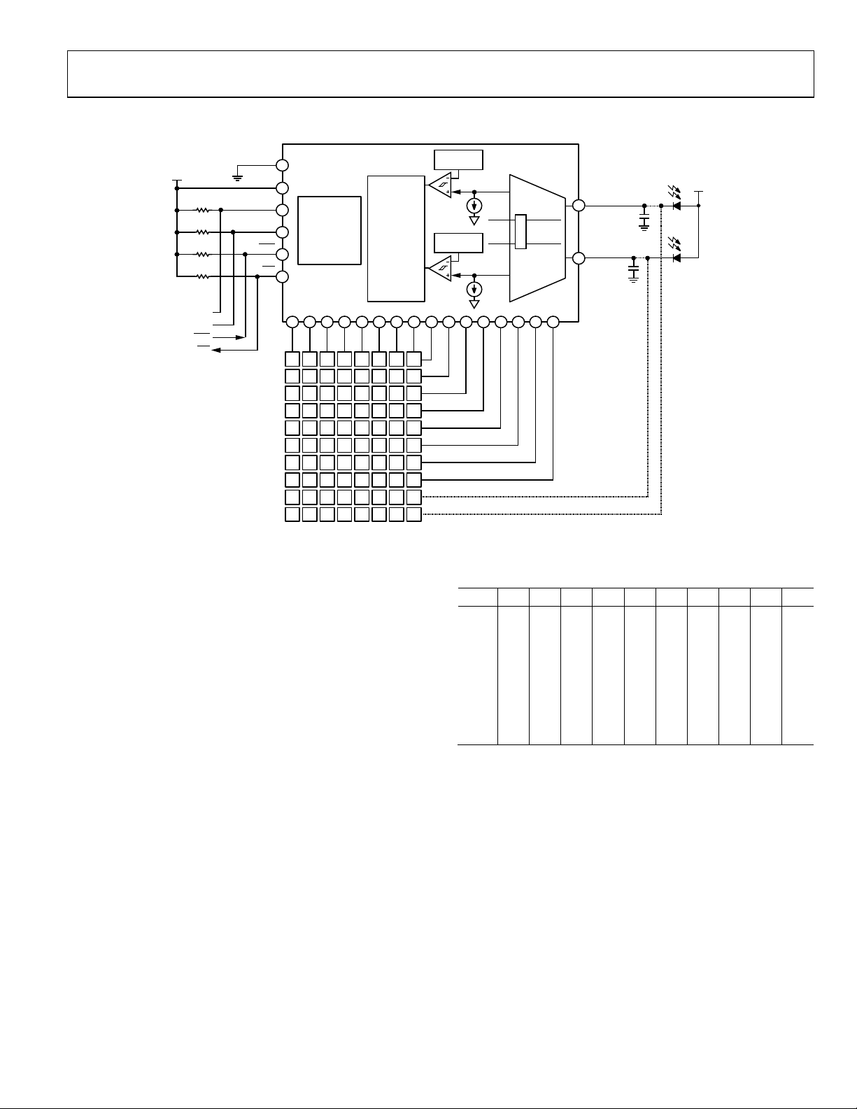
Figure 4. Typical Operating Circuit
The ADP5588 is a GPIO expander that can be configured either
as an 18-I/O port expander or as a 10 column × 8 row keypad
matrix (80 keys maximum). It is ideal for cellular phone designs
and other portable devices that require a large extended keypad
Table 10. Key Event Number Assignment Table
Row C0 C1 C2 C3 C4 C5 C6 C7 C8 C9
1 2 4 4 5 6 7 8 9 10
R0
11 12 13 14 15 16 17 18 19 20
R1
and/or expanded I/Os (see the Applications Information section
for various configurations). When smaller size keypads are
required, unused GPIOs in the keypad matrix can be used as
31 32 33 34 35 36 37 38 39 40
R3
41 42 43 44 45 46 47 48 49 50
I/Os (GPOs and GPIs). Two of the columns (C8 and C9) can
also be configured as comparator inputs for single or dual light
sensors. All GPIOs (rows and columns) default as GPIs at powerup with pull-ups and debounce enabled.
KEYPAD OPERATION
Any number of rows and columns, up to 10 columns × 8 rows,
can be configured to be part of the keypad matrix. The rows
and columns that make up the keypad matrix must be configured by setting the corresponding bits in Register 0x1D
through Register 0x1F. Keys on the keypad matrix appear on
the key event table with a decimal value of 1 (0x01 hexidecimal
or 0000001 binary) and run through 80 decimals (0x50 hexidecimal or 1010000 binary). See Ta b l e 10 for key event number
assignments. The keypad, in idle mode, is configured with
columns being driven low and rows as inputs high with pull-ups.
Rev. C | Page 7 of 28
61 62 63 64 65 66 67 68 69 70
R6
71 72 73 74 75 76 77 78 79 80
R7
When one key press or multiple key presses (short between
coumn and row) occur, the internal state machine checks the
row pins to determine which one is driven low and then triggers
an interrupt. The state machine then starts a key scan cycle to
determine which keys are pressed. After a key has been pressed
for 25 ms, the state machine sets the appropriate key(s) in the
key event status register with the key-pressed bits set (the MSB
in the key event register) in the order detected. If the KE_IEN
field in Register 0x01 is set, the state machine then sets the
KE_INT field in Register 0x01 and generates an interrupt to the
host processor.
ADP5588 Data Sheet
KEYPAD SCAN AND DECODE
D0_PULL
J7
I7
H7
G7
F7
E7
D7
C7
B7
A7
J6
I6
H6
G6
F6
E6
D6
C6
B6
A6
J5
I5
H5
G5
F5
E5
D5
C5
B5
A5
J4
I4
H4
G4
F4
E4
D4
C4
B4
A4
J3
I3
H3
G3
F3
E3
D3
C3
B3
A3
J2
I2
H2
G2
F2
E2
D2
C2
B2
A2
J1
I1
H1
G1
F1
E1
D1
C1
B1
A1
J0
I0
H0
G0
F0
E0
D0
C0
B0
A0
R7 R6 R5 R4 R3 R2 R1
R0
C0 C1 C2 C3 C4 C5 C6 C7 C9C8
10 × 8 KEYPAD MATRI X
V
CC
D1_PULL
D2_PULL
D3_PULL
D4_PULL
D5_PULL
D6_PULL
D7_PULL
07673-010
E4
Released
9
7 C 0 0000001
Key A0 released
To prevent glitches or narrow press times registering as valid
key presses, the key scanner requires the key to be pressed for
two scan cycles. The key scanner has a sampling period of 25 ms,
so the key must be pressed and held for at least 25 ms to register
as pressed. If the key is continuously pressed, the key scanner
continues to sample every 25 ms. If a key that was pressed is
released for 25 ms or greater, the state machine sets the appropriate keys in the key event status register with the key pressed
bits cleared in the order detected. Because the release of a key is
not necessarily in sync with the key scan sampling period, it may
take between 25 ms and 50 ms for a key to register as released.
After the key is registered as released, the key scanner goes back
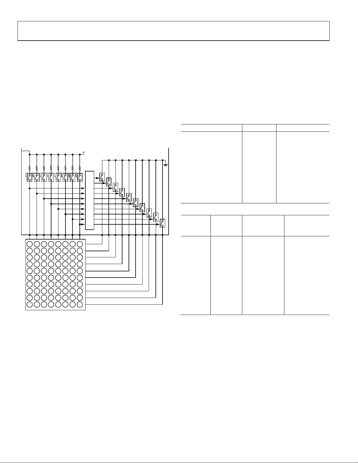
to idle mode. Figure 5 shows the row and column pins
connected to a typical 10 × 8, 80-switch keypad matrix.
The first read of any of the FIFO registers displays the first
event that happened and its status. Subsequent reads of the
same register replace the register data with the next event that
happens. If tracking of all the events is important, it is best to
used a single register per event. After all the events in the FIFO
are read, reading of any of the event registers yields a zero value.
Table 11 and Tabl e 12 show the event sequences as they are
logged in and read from the FIFO. The 10 FIFO registers are
labeled A through J, and keys are labeled A0 through J7.
Table 11. Example of Event Sequence
Key Pressed/Released Status Key Event Counter
A0 Pressed 1
B1 Pressed 2
A0 Released 3
C2 Pressed 4
B1 Released 5
D3 Pressed 6
C2 Released 7
E4 Pressed 8
D3 Released 10
Key Event Tracking
The 10-key event registers are set to act as a FIFO, meaning that
reading any of the 10-key event registers yields the key events in
the order they were pressed and released.
Tracking of key events is done with the help of the key event
counter (the KEC field in Register 0x03) and the FIFO/key
event registers (Register 0x04 through Register 0x0D). The KEC
count increases as keys are pressed and released; up to 10 events
can be logged in the count e r. The FIFO/key event registers, on
the other hand, display the key events and their status (pressed
or released) as they are read out of the FIFO. The FIFO registers
are made of eight bits, with the MSB dedicated as the status bit
(1 indicates a press and 0 indicates a release); the remaining
seven bits are used to display binary representation of the keys
that are pressed or released.
Figure 5. Keypad Decode Configuration
Rev. C | Page 8 of 28
Table 12. Interpretation of FIFO Event Reading
Key Event
Register
Interpretation
Key Event
Counter
Key Event
Register
Read
Key Event Register Content
(Binary)
1
10 N/A N/A N/A
9 D 1 0000001 Key A0 pressed
8 E 1 0001100 Key B1 pressed
6 F 1 0010111 Key C2 pressed
5 G 0 0001100 Key B1 released
4 A 1 0100010 Key D3 pressed
3 B 0 0010111 Key C2 released
2 H 1 0101101 Key E4 pressed
1 J 0 0101101 Key E4 released
0 I 0 0100010 Key D3 released
1
The first number indicates a key press or key release in Bit 7 of the key event
register: 1 = key press; 0 = key release.
Key Event Overflow
The ADP5588 is equipped with an overflow feature to handle
key events beyond the FIFO capacity. When all events are filled, any
additional events set the OVR_FLOW_INT bit in Register 0x02;
if the OVR_FLOW_IEN bit in Register 0x01 is set, the host
processor is also interrupted when overflow occurs. When the
FIFO is not full, new events are added as the last events.
The OVR_FLOW_M bit in Register 0x01 sets the mode of
operation during overflows. Clearing the OVR_FLOW_M bit
causes new incoming events to be discarded, and setting this bit
rolls over and overwrites old data with new data starting at the
first event.
Data Sheet ADP5588
KP_MODE
KEC
REG. 0x1D
THROUGH 0x1F
REG. 0x03
READ KE(s) TO CLEAR
INT DRIVE
KE_INT
REG. 0x02
WRITE 1 TO CLEAR
KE_IEN
REG. 0x01
07673-011
AND
DEBOUNCE
GPIOx
Dx_DIR
Dx_OUT
Dx_IN
Dx_IN_DBNC
Dx_PULL
V
CC
V
CC
07673-012
Autoincrement
The ADP5588 features automatic increment during I2C read
access. This allows the user to increment the address pointer
without having to send a read command for subsequent
addresses. This minimizes processor intervention and, therefore,
saves processor bandwidth and current drain. Bit 7 of Register 0x01
must be set to initiate autoincrement (see Figure 16 for the full
write and read sequence).
Key Event Interrupt
On a key event (KE) interrupt, the processor reads the interrupt
register to determine the cause of the interrupt. If the KE_INT
bit in Register 0x02 is the cause of the interrupt, the state
machine sets the KE_INT bit and reads the key event count
from the KEC[3:0] field in Register 0x03 to determine the number
of events. It then reads the INT_STAT register (Register 0x02)
to make sure that no new events have come in. After all the
events are read, the KEC field is decremented to zero (KEC =0)
and the KE_INT bit can be cleared by writing a 1 to it. Both key
presses and key releases are capable of generating key event
interrupts. The KE_INT bit cannot be cleared, and the
INT
pin
cannot be deasserted, until the FIFO is cleared of all events.
display the unlock message. The host then reads the lock status
register to see if the keypad is unlocked. After the first key event
interrupt, the state machine does not interrupt the processor
again unless the correct sequence is keyed. The state machine
resets if the correct sequences are not keyed before the keypad
lock interrupt mask timer expires.
The state of the keypad lock interrupt mask bit (Register 0x01,
Bit 2) in the configuration register determines whether the
interrupt pin is asserted when the keylock interrupt status bit
(Register 0x02, Bit 2) is set. Setting the keylock interrupt mask
bit causes the
INT
pin to be asserted when the keylock interrupt
status bit is set in Register 0x02; clearing that bit masks the
interrupt, causing the interrupt pin not to respond to the keylock
interrupt status bit. The mask interrupt timer should be set for
the time that it takes for the LCD to dim or turn off so that, if a
key is pressed, the backlight is set to bright mode again or reset
to turn on the LCD.
When the unlock mask interrupt timer equals 0, only the
correct unlock sequence can generate an interrupt. Disabling
the unlock mask interrupt timer allows the processor to remain
undisturbed for situations in which the user has the phone in a
pocket or purse and the keys are constantly pressed. The flow
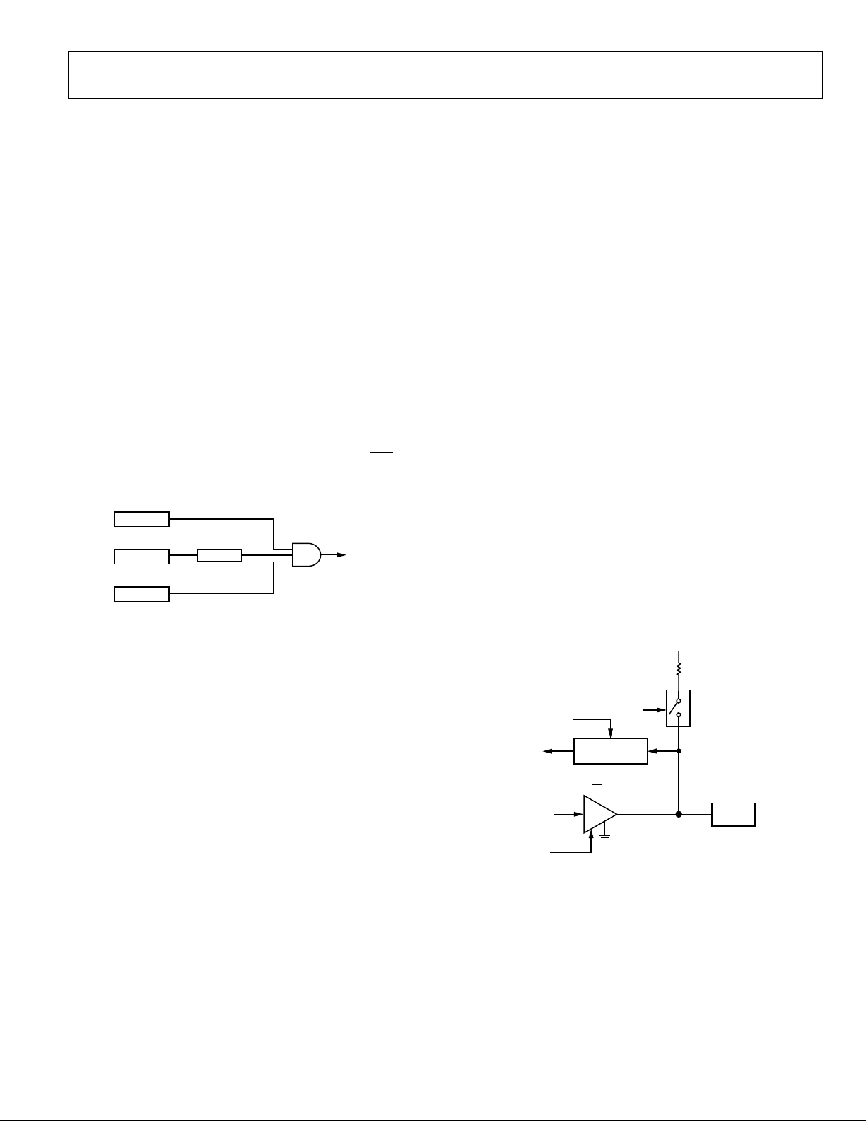
chart in Figure 6 shows the interaction of the interrupt mask
timer and interrupt generation.
Keypad Lock/Unlock Feature
The ADP5588 has a locking feature that allows the user to lock
the keypad or GPIs (configured to be part of the event table).
Once enabled, the keypad lock can prevent generation of key
event interrupts and key events to be recorded in the key event
table. This feature comprises the Unlock Key 1 and Unlock Key 2
registers (Register 0x0F and Register 0x10), the keypad lock
interrupt mask, the keypad unlock timers (Register 0x0E),
and the LCK1 and LCK2 bits, and the keylock enable bit
(Register 0x03).
The unlock keys can be programmed with any value of the keys
in the keypad matrix or any GPI values that are part of the key
event table. When the keypad lock interrupt mask timer is
enabled, the user must press two specific keys before a keylock
interrupt is generated or keypad events are recorded. After the
keypad is locked (set Bit 6, Register 0x03 to enable the lock), the
first time that the user presses any key, a key event interrupt is
generated. No additional interrupt is generated unless both
unlock key sequences are correct; then a keylock interrupt is
generated.
If the correct unlock keys are not pressed before the mask timer
expires, the state machine starts over. The first key event
interrupt is generated to allow the software to see that the user
has pressed a key so that the host can turn on the LCD and
Figure 6. Key Event Interrupt Generation
GENERAL-PURPOSE INPUTS AND OUTPUTS
The ADP5588 supports up to 18 programmable GPIOs that can
Rev. C | Page 9 of 28
be configured to address a variety of uses. Figure 7 shows the
makeup of a typical GPIO block where GPIOx represents any of
the 18 I/O lines.
General Purpose Inputs (GPI)
The ADP5588 allows the user to configure all or some of its
GPIOs into GPIs (general-purpose inputs). After the GPIOs are
configured as GPIs, the user can opt to also turn on pull-up
resistors and interrupt generation capability, thus reducing the
amount of software monitoring and processor interaction and
saving p ower.
The programmed level of the GPI interrupt determines the
active level of the GPI pin. For example, if a GPI interrupt level
Figure 7. Typical GPIO Block
 Loading...