QWERTY Keypad Controller
ADP5587
18
17
19
21
23
22
20
24
CONTROL
REGISTERS
CONTROL
INTERFACE
R7R6R5R4R3R2R1R0C0C1C2C3C4C5C6
C7
C9
C8
GND
V
CC
SCL
SDA
RST
INT
3 4 5 6 7 8 9 10 11 12 13 14 15 161 2
ADP5587
08612-001
Rev. D
Information furnished by Analog Devices is believed to be accurate and reliable. However, no
Trademarks and registered trademarks are the property of their respective owners.
Fax: 781.461.3113 ©2009-2012 Analog Devices, Inc. All rights reserved.
Data Sheet
FEATURES
18-GPIO port expander or 10 × 8 keypad matrix
GPIOs configurable as GPIs, GPOs, and keypad rows or
columns
2
I
C interface with auto-increment
1.65 V to 3.6 V operation
Keypad lock capability
Open-drain interrupt output
Key press and key release interrupts
GPI interrupt with level programmability
Programmable pull-ups
Key event counter with overflow interrupt
275 μs debounce on the reset line and GPIs
1 μA typical idle current
55 μA typical polling current
4 mm × 4 mm LFCSP package
Small 2 mm x 2 mm WLCSP package, 0.4 mm pitch
Multiple I
2
C addresses available for the LFCSP package to
allow multiple port expanders on the same bus
Mobile I/O Expander and
FUNCTIONAL BLOCK DIAGRAM
Figure 1.
APPLICATIONS
Keypad and I/O expander designed for QWERTY type phones
that require a large keypad matrix
GENERAL DESCRIPTION
The ADP5587 is an I/O port expander and keypad matrix
designed for QWERTY type phones that require a large keypad
matrix and expanded I/O lines. I/O expander ICs are used in
mobile platforms as a solution to the limited number of GPIOs
available in the main processor.
In its small 2 mm × 2 mm package, the ADP5587 contains
enough power to handle all key scanning and decoding and
to flag the processor of key presses and releases via the I
interface and interrupt. The ADP5587 frees the main microprocessor from the need to monitor the keypad, thereby
minimizing current drain and increasing processor bandwidth.
The ADP5587 is also equipped with a buffer/FIFO and key
event counter to handle and keep track of up to 10 unprocessed
key or GPI events with overflow wrap and interrupt capability.
The ADP5587 has keypad lock capability with an option to
trigger or not trigger an interrupt at key presses and releases.
2
C
All communication to the main processor is done using one
interrupt line and two I
2
C-compatible interface lines. The
ADP5587 can be configured as a keypad matrix of up to 8 rows ×
10 columns (a maximum of 80 keys).
When the ADP5587 is used for smaller keypad matrices, unused
row and column pins can be reconfigured to act as generalpurpose inputs or outputs. R0 to R7 denote the row pins of the
matrix, whereas C0 to C9 denote the column pins. At power-up,
all rows and columns default to GPIs and must be programmed
to function as part of the keypad matrix or as GPOs.
Two options for I
2
C addresses exist for the LFCSP package to
reduce the chance of port contention and allow up to two
ADP5587 ICs to operate on the same I
2
C bus (see the Ordering
Guide).
responsibility is assumed by Analog Devices for its use, nor for any infringements of patents or other
rights of third parties that may result from its use. Specifications subject to change without notice. No
license is granted by implication or otherwise under any patent or patent rights of Analog Devices.
One Technology Way, P.O. Box 9106, Norwood, MA 02062-9106, U.S.A.
Tel: 781.329.4700
www.analog.com

ADP5587 Data Sheet
TABLE OF CONTENTS
Features .............................................................................................. 1
Applications ....................................................................................... 1
Functional Block Diagram .............................................................. 1
General Description ......................................................................... 1
Revision History ............................................................................... 2
Specifications ..................................................................................... 3
DC Characteristics ....................................................................... 3
AC Characteristics ........................................................................ 4
Absolute Maximum Ratings ............................................................ 5
Thermal Resistance ...................................................................... 5
ESD Caution .................................................................................. 5
Pin Configurations and Function Descriptions ........................... 6
REVISION HISTORY
1/12—Rev. C to Rev. D
Changes to Table 11 .......................................................................... 9
Changes to Table 25 ........................................................................ 18
7/11—Rev. B to Rev. C
Changes to Features and General Description,
2
I
C Address Options ........................................................................ 1
Changes to the I
Figure 16, Figure, 17, and Figure 18 ............................................. 14
Changes to Ordering Guide .......................................................... 23
5/10—Rev. A to Rev. B
Changes to Features .......................................................................... 1
Changes to Table 1 ............................................................................ 3
Changes to Table 8 ............................................................................ 6
2
C Programming and Digital Control Section,
Typical Performance Characteristics ..............................................7
Theory of Operation .........................................................................8
Keypad Operation .........................................................................8
General-Purpose Inputs and Outputs ..................................... 12
I2C Programming and Digital Control ........................................ 14
Registers ....................................................................................... 15
Register Descriptions ................................................................. 16
Applications Information .............................................................. 21
Applications Overview .............................................................. 21
Keypad Current .......................................................................... 21
Outline Dimensions ....................................................................... 23
Ordering Guide .......................................................................... 23
3/10—Rev. 0 to Rev. A
Added WLCSP Information ........................................ Throughout
Added Typical Performance Characteristics Section ................... 7
Updated Outline Dimensions, Changes to Ordering Guide .... 23
12/09—Revision 0: Initial Version
Rev. D | Page 2 of 24

Data Sheet ADP5587
With One Key Press
ICC
VCC = 1.8 V, TA = −40°C to +85°C
55
90
μA
SPECIFICATIONS
TA = TJ = −40°C to +85°C, unless otherwise noted.
DC CHARACTERISTICS
Table 1. General DC Electrical Characteristics
Parameter Symbol Conditions Min Typ Max Unit
SUPPLY VOLTAGE
VCC Input Voltage Range VCC 1.65 3.6 V
Supply Current1 ICC VCC = 1.8 V to 3.0 V, TA = −40°C to +85°C 1 10 μA
ICC VCC = 3.0 V, TA = −40°C to +85°C 100 200 μA
With GPI Low (Pull-Up Enabled)2 ICC VCC = 1.8 V to 3.0 V, TA = −40°C to +85°C 20 50 μA
With GPI Low (Pull-Up Disabled) ICC VCC = 1.8 V to 3.0 V, TA = −40°C to +85°C 2 10 μA
With One GPO Active3 ICC VCC = 1.8 V, TA = −40°C to +85°C 50 μA
OSCILLATOR CURRENT
Oscillator Current (Enabled) ICC VCC = 1.8 V to 3.0 V 40 μA
1
Operating current measured with I/Os defaulting as GPIs, with all pull-ups enabled and all inputs open.
2
With one GPI low.
3
Load = 100 kΩ.
Table 2. I/O DC Electrical Characteristics
Parameter Symbol Conditions Min Typ Max Unit
INPUT LOGIC LEVELS (SCL, SDA,
Logic Low Input Voltage VIL 1.8 V ≤ VIO ≤ 3.0 V 0.3 × VCC V
Logic High Input Voltage VIH 1.8 V ≤ VIO ≤ 3.0 V 0.7 × VCC V
Schmitt Trigger Hysteresis V
Input Leakage Current V
OUTPUT LOGIC LEVELS (C0 to C9, R0 to R7)
Logic Low Output Voltage VOL I
Output High Voltage VOH I
OUTPUT LOGIC LEVELS (
INT
Output Low Voltage VOL I
Output High Voltage VOH 1.8 V ≤ VCC ≤ 3.0 V 0.7 × VCC V
Logic High Leakage Current V
PULL-UP RESISTANCE FOR GPIOs (C0 to C9, R0 to R7)2 R
1
Power-up default current. All I/Os default to GPIs and are open; C8 and C9 default to GPIs; I2C is idle.
2
GPIO internal pull-ups are approximately 100 kΩ.
, C0 to C9, R0 to R7)1
RST
0.10 V
HYST
1.8 V ≤ VIO ≤ 3.0 V −1 +1 µA
I-LEAKAGE
= 1 mA 0.40 V
SINK
= 1 mA VCC − 0.3 V V
SOURCE
, SDA)
= 3 mA,
SINK
1.8 V ≤ V
1.8 V ≤ VCC ≤ 3.0 V 0.1 1 µA
O-LEAKAG E
100 kΩ
PULL-UP
≤ 3.0 V
CC
0.40 V
Table 3. Capacitance Loading1
Parameter Symbol Min Typ Max Unit
I/O Input Capacitance CIN 1 10 pF
I/O Output Loading Capacitance C
Capacitive Load for Each Bus Line C
1
Guaranteed by design.
2
CB = total capacitance of one bus line in picofarads.
50 pF
OUT
2
400 pF
B
Rev. D | Page 3 of 24

ADP5587 Data Sheet
Setup Time for Stop Condition
tSU,
0.6
μs
SDA
SCL
S
S = START CONDITION
Sr = REPEATED S TART CONDITION
P = STOP CONDITION
Sr P S
t
LOW
t
R
t
HD, DAT
t
HIGH
t
SU, DAT
t
F
t
F
t
SU, STA
t
HD, STA
t
SP
t
SU, STO
t
BUF
t
R
08612-002
AC CHARACTERISTICS
Table 4. General AC Characteristics1
Parameter Symbol Min Typ Max Unit
Delay from Reset Deassertion to I2C Access R
Keypad Unlock Timer T
Keypad Interrupt Mask Timer T
Debounce TD 275 μs
1
Guaranteed by design.
Table 5. I2C AC Electrical Characteristics1
Parameter Symbol Min Ty p Max Unit
SCL Clock Frequency f
SCL High Time t
SCL Low Time t
Data Setup Time tSU,
Data Hold Time tHD,
Setup Time for Repeated Start tSU,
Hold Time for Start/Repeated Start tHD,
Bus Free Time for Stop and Start t
Rise Time for SCL and SDA2 tR 20 + 0.1 CB 300 ns
Fall Time for SCL and SDA2 tF 20 + 0.1 CB 300 ns
Pulse Width of Suppressed Spike tSP 0 50 μs
1
Guaranteed by design.
2
tR and tF are measured between 0.3 × VCC and 0.7 × VCC.
60 μs
STD
7 sec
KUT
31 sec
KIMT
400 kHz
SCL
0.6 μs
HIGH
1.3 μs
LOW
100 ns
DAT
0 0.9 μs
DAT
0.6 μs
STA
0.6 μs
STA
1.3 μs
BUF
STO
2
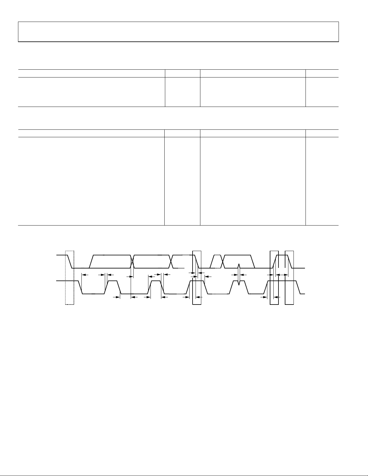
Figure 2. I
C Interface Timing Diagram
Rev. D | Page 4 of 24

Data Sheet ADP5587
ABSOLUTE MAXIMUM RATINGS
Table 6.
Parameter Rating
VCC −0.3 V to + 4.0 V
R0 to R7, C0 to C9 −0.3 V to VCC + 0.3 V
SCL −0.3 V to VCC + 0.3 V
SDA −0.3 V to VCC + 0.3 V
−0.3 V to VCC + 0.3 V
RST
−0.3 V to VCC + 0.3 V
INT
GND −0.3 V to +0.3 V
Operating Ambient Temperature Range −40°C to +85°C
Operating Junction Temperature Range −40°C to +125°C
Storage Temperature Range −65°C to +150°C
ESD Machine Model ±200 V
ESD Human Body Model ±2000 V
ESD Charged Device Model ±1000 V
Soldering Condition JEDEC J-STD-020
Stresses above those listed under Absolute Maximum Ratings
may cause permanent damage to the device. This is a stress
rating only; functional operation of the device at these or any
other conditions above those indicated in the operational
section of this specification is not implied. Exposure to absolute
maximum rating conditions for extended periods may affect
device reliability.
THERMAL RESISTANCE
θJA is specified for the worst-case conditions, that is, a device
soldered in a circuit board for surface-mount packages.
Table 7. Thermal Resistance
Package Type θJA θJC Unit
24-Lead LFCSP_WQ 57.8 9.4 °C/W
Maximum Power 600 N/A mW
25-Ball WLCSP 46 N/A °C/W
Maximum Power 600 N/A mW
ESD CAUTION
Rev. D | Page 5 of 24

ADP5587 Data Sheet
08612-003
2
1
3
4
5
6
18
17
16
15
14
13
R2
R3
R4
R5
R6
R7
C4
NOTES
1. EXPOSED
PAD MUST BE CONNECTED
TO GROUND.
C5
C6
C7
C8
C9
8
9
10
11
7
R0
C0
C1
C2
12
C3
R1
20
19
21
RST
GND
VCC
22
SDA
23
SCL
24
INT
ADP5587
TOP
VIEW
(Not to S cale)
INT
RST
TOP VIEW
(BALL SIDE DO WN)
Not to Scale
08612-004
1
A
B
C
D
E
2 3 4
BALL A1
CORNER
C6 C1 R2 R7
VCC C7 C2 NC R6
SDA C8 C3 R1 R5
SCL C9 C4 R0 R4
GND C5 C0 R3
NOTES
1. NC = NO CONNECT.
5
6
A4
R2
GPIO, Row 2 in the Keypad Matrix.
PIN CONFIGURATIONS AND FUNCTION DESCRIPTIONS
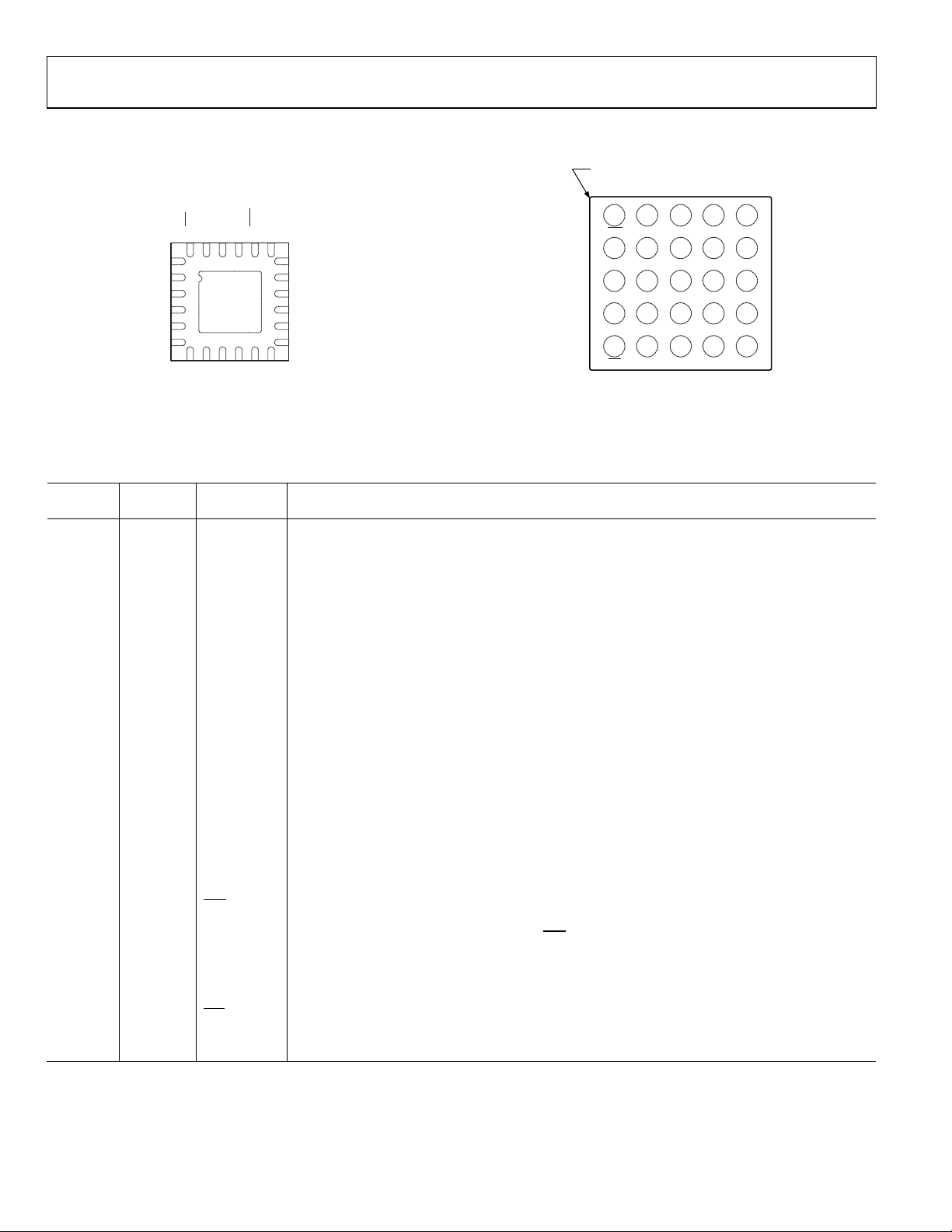
Figure 3. LFCSP Pin Configuration
Table 8. Pin Function Descriptions
LFCSP
Pin No.
WLCSP
Pin No.
1 A5 R7 GPIO, Row 7 in the Keypad Matrix.
2 B5 R6 GPIO, Row 6 in the Keypad Matrix.
3 C5 R5 GPIO, Row 5 in the Keypad Matrix.
4 D5 R4 GPIO, Row 4 in the Keypad Matrix.
5 E5 R3 GPIO, Row 3 in the Keypad Matrix.
N/A B4 N/A No Connect (NC)
7 C4 R1 GPIO, Row 1 in the Keypad Matrix.
8 D4 R0 GPIO, Row 0 in the Keypad Matrix.
9 E4 C0 GPIO, Column 0 in the Keypad Matrix.
10 A3 C1 GPIO, Column 1 in the Keypad Matrix.
11 B3 C2 GPIO, Column 2 in the Keypad Matrix.
12 C3 C3 GPIO, Column 3 in the Keypad Matrix.
13 D3 C4 GPIO, Column 4 in the Keypad Matrix.
14 E3 C5 GPIO, Column 5 in the Keypad Matrix.
15 A2 C6 GPIO, Column 6 in the Keypad Matrix.
16 B2 C7 GPIO, Column 7 in the Keypad Matrix.
17 C2 C8 GPIO, Column 8 in the Keypad Matrix.
18 D2 C9 GPIO, Column 9 in the Keypad Matrix.
19 E2 GND Ground.
20 A1
21 B1 VCC Supply Voltage, 1.65 V to 3.6 V.
22 C1 SDA I2C Serial Data. The open drain requires an external pull-up resistor.
23 D1 SCL I2C Clock.
24 E1
EP N/A EPAD Exposed Pad. The exposed pad must be connected to ground.
Figure 4. WLCSP Pin Configuration
Mnemonic Description
Hardware Reset (Active Low). This pin resets the device to the power default conditions. The reset
RST
pin must be driven low for a minimum of 50 μs to be valid and to prevent false resets due to ESD
glitches or noise in the system. If not used,
Processor Interrupt, Active Low, Open Drain. This pin can be pulled up to 2.7 V or 1.8 V for selection
INT
must be tied high with a pull-up resistor.
RST
flexibility in the processor GPIO supply group.
Rev. D | Page 6 of 24

Data Sheet ADP5587
3.5
3.0
2.5
2.0
1.5
1.0
0.5
0
–40 –20 0 20 40 60 80 100
TEMPERATURE (°C)
I
CC
CURRENT (µA)
08612-017
VCC AT 1.8V
VCC AT 3.0V
140
120
100
80
60
40
20
0
–40 –20 0 20 40 60 80 100
TEMPERATURE (°C)
INPUT/OUTPUT V
OH
(mV)
08612-019
VCC AT 1.8V
VCC AT 3.0V
60
50
40
30
20
10
0
–40 –20 0 20 40 60 80 100
TEMPERATURE (°C)
INPUT/OUTPUT V
OL
(mV)
08612-018
VCC AT 1.8V
V
CC
AT 3.0V
1.7
1.6
1.5
1.4
1.3
1.2
1.1
1.0
0.9
0.8
0.7
1.7 1.9 2.1 2.3 2.5 2.7 2.9 3.1 3.3
SUPPLY VOLTAGE (V)
STANDBY CURRENT ( µ A)
08612-020
TYPICAL PERFORMANCE CHARACTERISTICS
TA = 25°C, unless otherwise specified.
Figure 5. Standby (ICC) Current vs. Temperature
Figure 6. Input/Output VOH vs. Temperature (Source Current = 1 mA)
Figure 7. Input/Output VOL vs. Temperature (Sink Current = 1 mA)
Figure 8. Supply Voltage vs. Standby Current
Rev. D | Page 7 of 24

ADP5587 Data Sheet
CONTROL
REGISTERS
CONTROL
INTERFACE
R7R6R5R4R3R2R1R0C0C1C2C3C4C5C6
C7
C9
C8
A0A1
A2A3
A4
A5A6
A7
B0B1B2B3B4B5B6B7
C0C1C2C3C4C5C6C7
D0D1D2D3D4D5D6D7
E0E1E2E3E4E5E6E7
F0F1F2F3F4F5F6F7
G0G1G2G3G4G5G6G7
H0H1H2H3H4H5H6H7
I0I1I2I3I4I5I6I7
J0J1J2J3J4J5J6J7
SCL
SDA
RST
INT
V
CC
GND
V
CC
SCL
SDA
19
21
23
22
18
17
20
24
1
2 3
4
5 6
7 8
9
10 11 12 13 14 15 16
ADP5587
RST
INT
08612-005
THEORY OF OPERATION
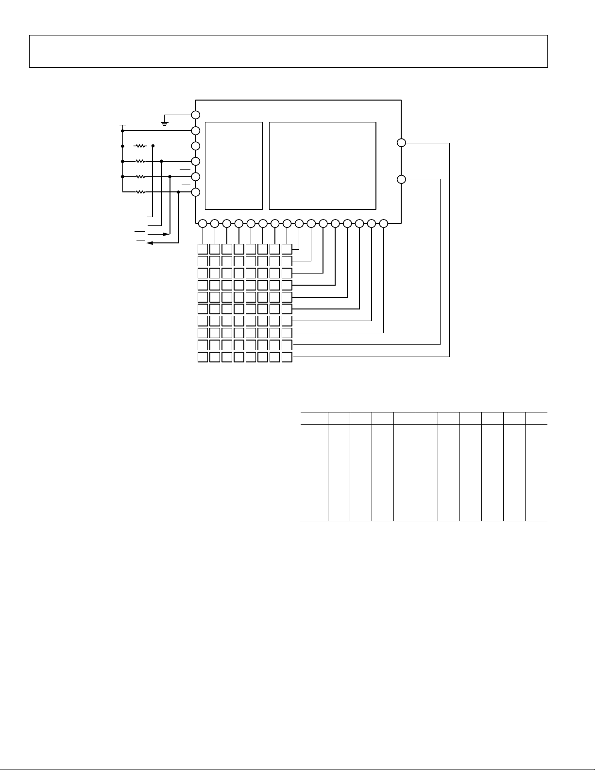
Figure 9. Typical Operating Circuit
The ADP5587 is a GPIO expander that can be configured either
as an 18 I/O port expander or as a 10 column × 8 row keypad
matrix (80 keys maximum). It is ideal for cellular phone designs
and other portable devices that require a large extended keypad
and/or expanded I/Os. When smaller size keypads are required,
unused GPIOs in the keypad matrix can be used as I/Os (GPOs
and GPIs). All GPIOs (rows and columns) default to GPIs at
power-up with pull-ups and debounce enabled.
KEYPAD OPERATION
Any number of rows and columns, up to 10 columns × 8 rows,
can be configured to be part of the keypad matrix. The rows and
columns that make up the keypad matrix must be configured by
setting the corresponding bits in Register 0x1D to Register 0x1F.
Key presses and releases appear in the key event table/registers
with a decimal value of 1 (0x01 hexadecimal or 0000001 binary)
through a decimal value of 80 (0x50 hexadecimal or 1010000
binary). See Ta b l e 9 for key event number assignments. The
keypad, in idle mode, is configured with columns driven low
and rows as inputs configured high with pull-up resistors.
Rev. D | Page 8 of 24
Table 9. Key Event Number Assignment Table
Row C0 C1 C2 C3 C4 C5 C6 C7 C8 C9
1 2 3 4 5 6 7 8 9 10
R0
11 12 13 14 15 16 17 18 19 20
R1
21 22 23 24 25 26 27 28 29 30
R2
31 32 33 34 35 36 37 38 39 40
R3
41 42 43 44 45 46 47 48 49 50
R4
51 52 53 54 55 56 57 58 59 60
R5
61 62 63 64 65 66 67 68 69 70
R6
71 72 73 74 75 76 77 78 79 80
R7
When one key press or multiple key presses (short between
column and row) occur, the internal state machine checks the
row pins to determine which one is driven low and then triggers
an internal interrupt. The state machine then starts a key scan
cycle to determine which columns are involved in the key press.
After a key has been pressed for 25 ms, the state machine sets
the appropriate key number in the key event status register with
the key-pressed bits set (the MSB in the key event register) in
the order detected. The state machine then sets the KE_INT bit
in Register 0x02. If the KE_IEN field in Register 0x01 is set, an
interrupt is sent to the host processor.
 Loading...