Programmable Current Backlight Driver
FEATURES
Efficient asynchronous boost converter for driving up to
6 white LEDs
2.7 V to 5.5 V input voltage range
128 programmable backlight LED current levels (30 mA
maximum)
Programmable backlight fade-in/fade-out times
Programmable backlight dim and off times
Ambient light sensing with autonomous backlight
adjustment
3 auxiliary LED current sinks
64 programmable auxiliary LED current levels (14 mA
maximum)
Programmable auxiliary LED fade-in/fade-out times
Programmable auxiliary LED on and off times (allows
blinking)
2
I
C-compatible serial interface
Interrupt line for signaling an external processor (
Hard reset (
RST
)
Current limit protection
Thermal overload protection
Available in small 4.0 mm × 4.0 mm, 24-lead LFCSP package
APPLICATIONS
Display backlight driver with ambient light sensor input and
control and multiple LED indicator sinks
INT
)
with Ambient Light Sensor Input
ADP5501
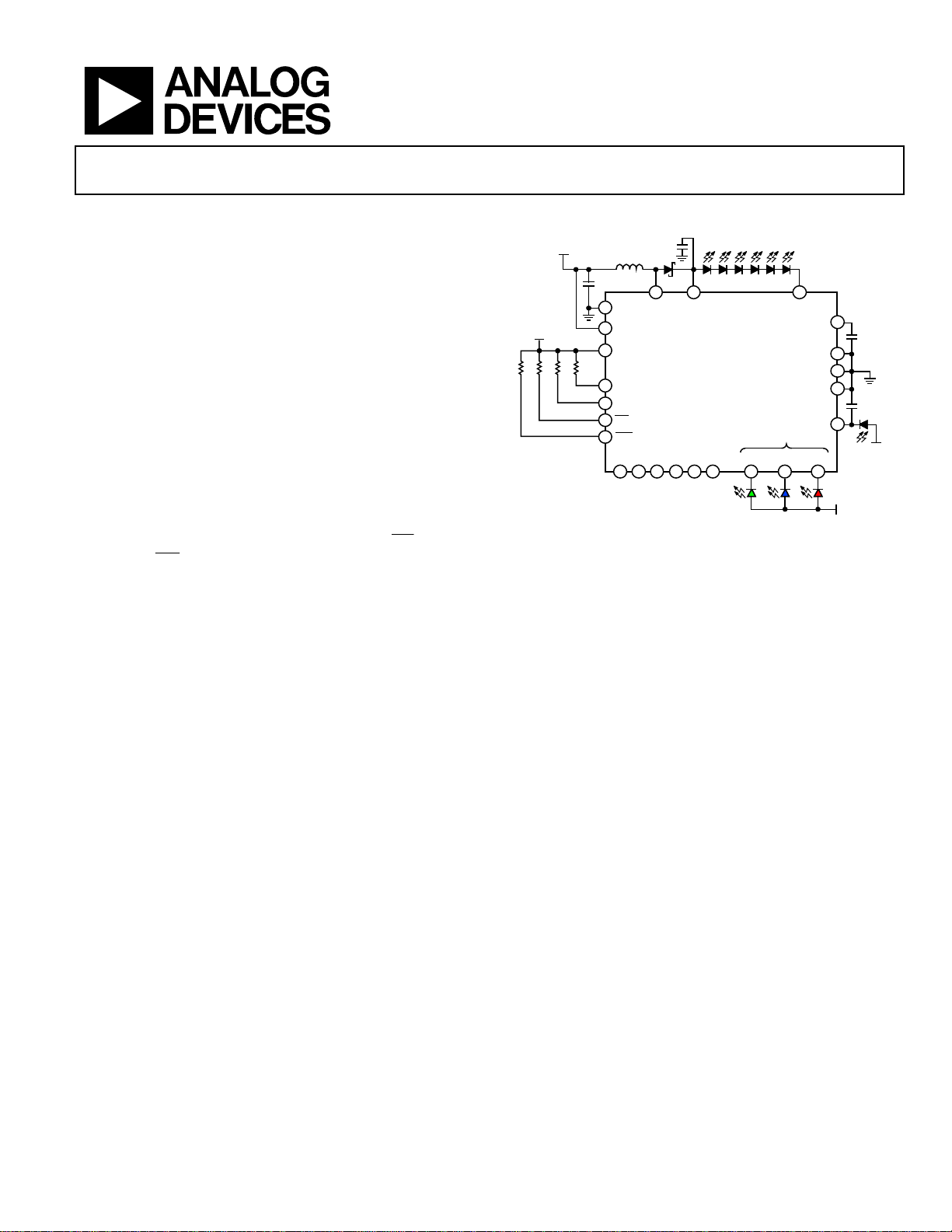
TYPICAL OPERATING CIRCUIT
2.7V TO 5.5V
I/O RAIL
10kΩ
1µF
1
21
16
10kΩ
2.2kΩ
2.2kΩ
5
4
3
15
1µF
4.7µH
2
SW22BST
PGND
VBAT
VDDIO
SCL
SDA
INT
RST
6NC7NC8NC9NC10NC11NC12
ADP5501
Figure 1.
LED1
BL_SNK
CAP_OUT
RGB
LED2
13
23
GND
GND
GND
CMP_IN
LED0
14
20
1µF
19
18
24
100nF
17
VBAT
3.3V
07780-001
GENERAL DESCRIPTION
The ADP5501 is a versatile, single-chip, white LED backlight
driver with programmable ambient light sensor input and
programmable LED current. This device is designed for mediaenabled handset applications. The ADP5501 uses an I
compatible serial interface and a single line interrupt to
communicate with the host processor.
Rev. 0
Information furnished by Analog Devices is believed to be accurate and reliable. However, no
responsibility is assumed by Analog Devices for its use, nor for any infringements of patents or other
rights of third parties that may result from its use. Specifications subject to change without notice. No
license is granted by implication or otherwise under any patent or patent rights of Analog Devices.
Trademarks and registered trademarks are the property of their respective owners.
2
C®-
The ADP5501 can detect ambient light levels and adjust the
backlight brightness accordingly, resulting in extended battery life.
Once configured, the ADP5501 is capable of controlling the
display backlight intensity, on/off timing, dimming, and fading
without the intervention of the main processor, which translates
into valuable battery power savings. The three auxiliary LEDs
are also capable of fading and are timed on and off via register
programming.
One Technology Way, P.O. Box 9106, Norwood, MA 02062-9106, U.S.A.
Tel: 781.329.4700 www.analog.com
Fax: 781.461.3113 ©2008 Analog Devices, Inc. All rights reserved.

ADP5501
TABLE OF CONTENTS
Features .............................................................................................. 1
Applications ....................................................................................... 1
Typical Operating Circuit ................................................................ 1
General Description ......................................................................... 1
Revision History ............................................................................... 2
Specifications ..................................................................................... 3
Absolute Maximum Ratings ............................................................ 5
Thermal Resistance ...................................................................... 5
ESD Caution .................................................................................. 5
Pin Configuration and Function Descriptions ............................. 6
Typical Performance Characteristics ............................................. 7
Theory of Operation ........................................................................ 9
Backlight Drive Control .............................................................. 9
Backlight Operating Levels ....................................................... 10
Backlight Maximum and Dim Settings ................................... 10
Backlight Turn-On/Turn-Off/Dim .......................................... 10
Automatic Dim and Turn-Off Timers ..................................... 11
Linear Backlight Fade-In and Fade-Out .................................. 11
Fade Override ............................................................................. 13
Advanced Fading (Square) ........................................................ 13
Advanced Fading (Cubic 1 and Cubic 2) ................................ 13
Ambient Light Sensing .............................................................. 14
Automatic Backlight Adjustment ............................................. 14
LED Current Sinks ..................................................................... 15
Interrupt Output (
Reset Input (
Communicaton Interface .............................................................. 18
Register Map ................................................................................... 19
Detailed Register Descriptions ..................................................... 20
Applications Information .............................................................. 26
Converter Topology ................................................................... 26
PCB Layout ................................................................................. 27
Example Circuit .......................................................................... 27
Outline Dimensions ....................................................................... 28
Ordering Guide .......................................................................... 28
INT
) ............................................................. 17
RST
) ....................................................................... 17
REVISION HISTORY
10/08—Revision 0: Initial Version
Rev. 0 | Page 2 of 28

ADP5501
SPECIFICATIONS
VBAT = 2.7 V to 5.5 V, TJ = −40C to +125C, unless otherwise noted.
Table 1.
Parameter Symbol Conditions1 Min Typ Max Unit
SUPPLY VOLTAGE
VBAT Input Voltage Range V
VDDIO Input Voltage Range VIO 1.8 3.3
Undervoltage Lockout Threshold UVLO
UVLO
UVLO
UVLO
SW Leakage SW
SUPPLY CURRENT
Shutdown Current3 I
Standby Current4 I
BACKLIGHT LED DRIVER (SW, BST)
Current Limit (Peak Inductor Current) 450 600 750 mA
On Resistance 200 200 400 mΩ
Overvoltage Threshold 24.5 27 29.5 V
Boost Startup Time 1 mS
BACKLIGHT LED CURRENT SINK (BL_SNK)
Full-Scale Current Sink
Backlight Current Ramp Rate Fade timers disabled 0.3 mA/ms
AMBIENT LIGHT SENSOR (CMP_IN)
Full-Scale Current BL
INPUT LOGIC LEVELS (SCL, SDA, RST)
Logic Low Input Voltage VIL 1.8 V ≤ VDDIO ≤ 3.3 V
Logic High Input Voltage VIH 1.8 V ≤ VDDIO ≤ 3.3 V
Input Leakage Current V
INPUT LOGIC DEBOUNCE (RST)
OPEN-DRAIN OUTPUT LOGIC LEVELS (INT, SDA)
Logic Low Output Voltage VOL I
Logic High Leakage Current V
AUX LED CURRENT SINKs (ILED, C3, R3)
Leakage LED
Full-Scale Current Sink LED
THERMAL SHUTDOWN
Thermal Shutdown Threshold TS TJ rising 150 °C
Thermal Shutdown Hysteresis TS
I2C TIMING SPECIFICATIONS
Delay from Reset Deassertion to I2C Access 60 s
SCL Clock Frequency f
SCL High Time t
SCL Low Time t
Data Setup Time t
Data Hold Time t
Setup Time for Repeated Start t
2.7 5.5 V
BAT
VBAT falling 1.7 2.1 V
VBAT
VBAT rising 2.4 2.7 V
VBAT
VDDIO falling 1.1 1.3 V
VDDIO
VDDIO rising 1.4 V
VDDIO
2.7 V ≤ VBAT ≤ 5.5 V 0.1 1 A
LEAKAGE
VDDIO = 0 V 0.1 1 A
SD
STNBY
1.8 V ≤ VDDIO ≤ 3.3 V
STNBY
= 0
Backlight code = 0x7F,
2
25 45 A
,
26 30 32 mA
2
V
bias = 0.65 V
0.7 1 1.2 mA
FULLSCALE
2
0.3 × VDDIO V
2
0.7 × VDDIO V
1.8 V ≤ VDDIO ≤ 3.3 V
I-LEAKAGE
2
0.1 1 µA
VIL-DBNC 50 75 100 s
= 1mA 0.4 V
OH-LEAKAGE
SINK
1.8 V ≤ VDDIO ≤ 3.3 V
2
0.1 1 µA
Sink disabled 0.1 1 µA
LEAKAGE
Applied pin voltage = 1 V 10.5 14 16.5 mA
FULLSCALE
T
HYS
400 kHz
SCL
0.6 s
HIGH
1.3 s
LOW
100 ns
SU, DAT
0 0.9 s
HD, DAT
0.6 s
SU, STA
falling 10 °C
J
Rev. 0 | Page 3 of 28
ADP5501
Parameter Symbol Conditions
Hold Time for Start/Repeated Start t
Bus Free Time for Stop and Start Condition t
Setup Time for Stop Condition t
0.6 s
HD, STA
1.3 s
BUF
0.6 s
SU, STO
1
Min Typ Max Unit
Rise Time for SCL and SDA tR 20 + 0.1 CB 300 ns
Fall Time for SCL and SDA tF 20 + 0.1 CB 300 ns
Pulse Width of Suppressed Spike tSP 0 50 s
5
Capacitive Load for Each Bus Line C
1
All limits at temperature extremes are guaranteed via correlation using standard statistical quality control (SQC). Typical values are at TA = 25°C, VBAT = 3.6 V.
2
3.3 V or VBAT, whichever is smaller.
3
Internal LDO powered down, digital blocks inactive, I2C inactive, boost inactive.
4
Internal LDO powered up, digital blocks active, I2C active, boost inactive.
5
C
is the total capacitance of one bus line in picofarads (pF).
B
B
400 pF
SDA
t
t
LOW
SCL
S
S = START CONDI TION
Sr = REPEATED START CONDITION
P = STOP CO NDITION
t
R
t
HD, DAT
t
SU, DAT
t
HIGH
t
F
t
SU, STA
t
F
t
HD, STA
Sr
t
SP
t
SU, STO
t
R
BUF
P S
07780-002
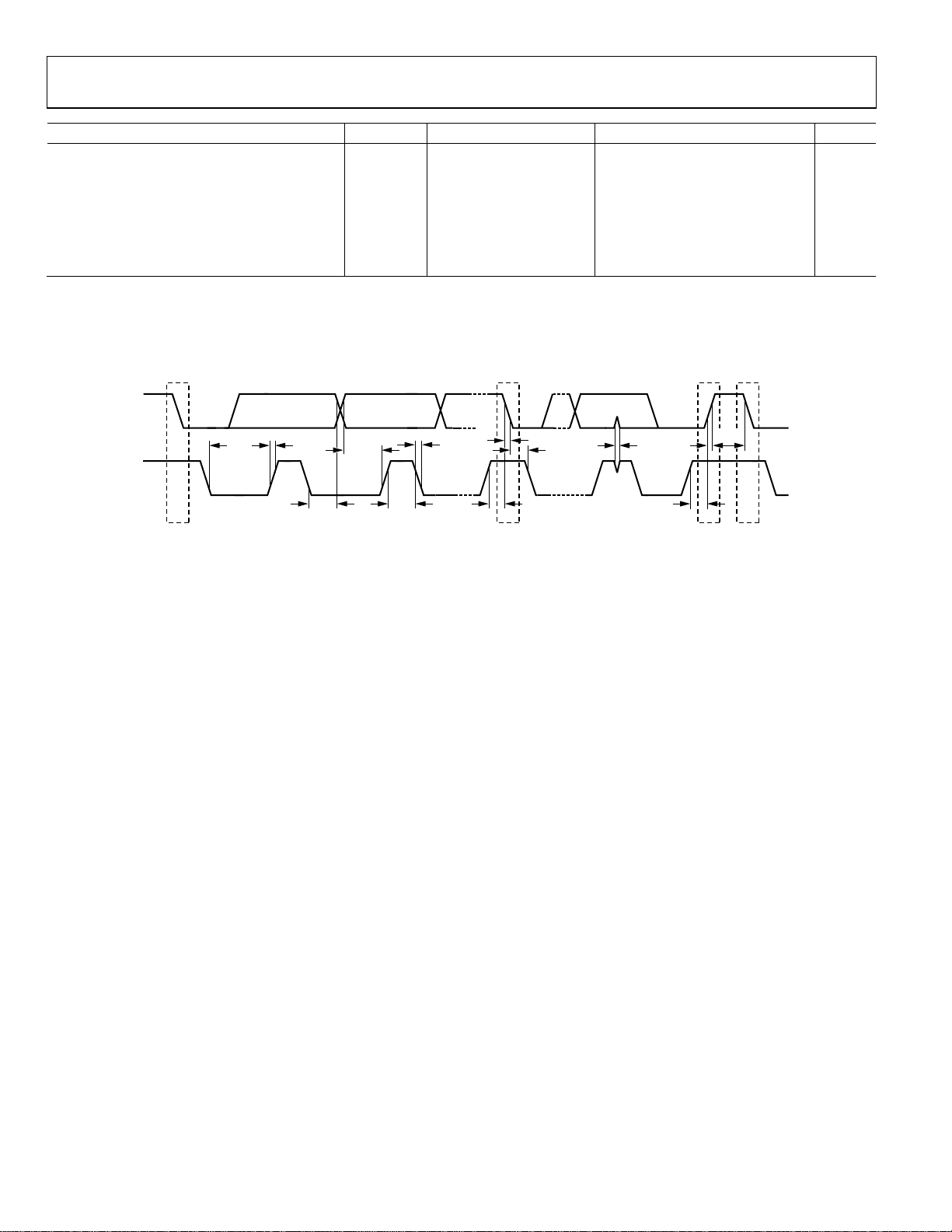
Figure 2. Interface Timing Diagram
Rev. 0 | Page 4 of 28
ADP5501
ABSOLUTE MAXIMUM RATINGS
Table 2.
Parameter Rating
VBAT to GND –0.3 V to +6 V
VDDIO to GND –0.3 V to VBAT
SW/BST to GND –0.3 V to +30 V
LED0/LED1/LED2/CMP_IN/SCL/SDA/INT/
RST/CAP_OUT/BL_SNK to GND
PGND to GND –0.3 V to +0.3 V
Operating Ambient Temperature Range −40°C to +85°C
Operating Junction Temperature Range –40°C to +125°C
Storage Temperature Range –65°C to +150°C
Soldering Conditions JEDEC J-STD-020
1
In applications where high power dissipation and poor thermal resistance
are present, the maximum ambient temperature may have to be derated.
Maximum ambient temperature (TA(MAX)) is dependent on the maximum
operating junction temperature (TJ(MAXOP) = 125°C), the maximum power
dissipation of the device (PD(MAX)), and the junction-to-ambient thermal
resistance of the part/package in the application (θJA), using the following
equation: TA(MAX) = TJ(MAXOP) – (θJA x PD(MAX)).
–0.3 V to +6 V
1
Stresses above those listed under Absolute Maximum Ratings
may cause permanent damage to the device. This is a stress
rating only; functional operation of the device at these or any
other conditions above those indicated in the operational
section of this specification is not implied. Exposure to absolute
maximum rating conditions for extended periods may affect
device reliability.
Absolute maximum ratings apply individually only, not in
combination. Unless otherwise specified, all other voltages are
referenced to GND.
THERMAL RESISTANCE
θJA is specified for the worst-case conditions, that is, a device
soldered in a circuit board for surface-mount packages.
Table 3. Thermal Resistance
Package Type θJA Unit
24-Lead LFCSP_VQ 50 ⁰C/W
ESD CAUTION
Rev. 0 | Page 5 of 28

ADP5501
PIN CONFIGURATION AND FUNCTION DESCRIPTIONS
VBAT
BST
BL_SNK
GND
CAP_OUT
GND
20
19
21
22
23
24
PIN 1
INDICATO R
1PGND
2SW
3
4SDA
5SCL
6NC
ADP5501
TOP VIEW
(Not to Scale)
9
7
8
C
C
C
N
N
N
INT
NOTES
1. NC = NO CONNECT .
2. EXPOSED P AD MUST BE CONNECT ED
TO GROUND.
Figure 3. Pin Configuration
Table 4. Pin Function Descriptions
Pin No. Mnemonic Description
1 PGND Power Switch Output to Ground.
2 SW Power Switch Input.
3
Processor Interrupt, Active Low, Open Drain. INT should be pulled up to VDDIO.
INT
4 SDA I2C-Compatible Serial Data Line (Open Drain Requires External Pull-Up) to VDDIO.
5 SCL I2C-Compatible Serial Clock Line (Open Drain Requires External Pull-Up) to VDDIO.
6 NC No Connect.
7 NC No Connect.
8 NC No Connect.
9 NC No Connect.
10 NC No Connect.
11 NC No Connect.
12 LED1 LED 1 Current Sink. LED1 can be used with LED0 and LED2 as RGB.
13 LED2 LED 2 Current Sink. LED2 can be used with LED1 and LED0 as RGB.
14 LED0 LED 0 Current Sink. LED0 can be used with LED1 and LED2 as RGB.
15
Reset Input, Active Low. This input signal resets the device to the power-up default conditions. It must be driven
RST
low for a minimum of 75 s (typical) to be valid.
16 VDDIO
Supply Voltage for the I/O Pin. The output pin can be 1.8 V to 3.3 V or VBAT, whichever is smaller. If VDDIO = 0,
the device goes into full shutdown mode.
17 CMP_IN Input for Ambient Light Sensing.
18 GND Ground.
19 GND Ground.
20 CAP_OUT
Capacitor for Internal 2.7 V LDO. A 1 F capacitor must be connected between this pin and ground. Do not use
this pin to supply external loads.
21 VBAT Main Supply Voltage for the IC (2.7 V to 5.5 V).
22 BST Overvoltage Monitor Input for the Boost Converter.
23 BL_SNK Backlight Current Sink.
24 GND Ground.
EPAD The exposed pad must be connected to ground.
18 GND
17 CMP_IN
16 VDDI O
15
RST
14 LED0
13 LED2
11
12
10
1
C
C
N
N
LED
07780-003
Rev. 0 | Page 6 of 28
ADP5501
TYPICAL PERFORMANCE CHARACTERISTICS
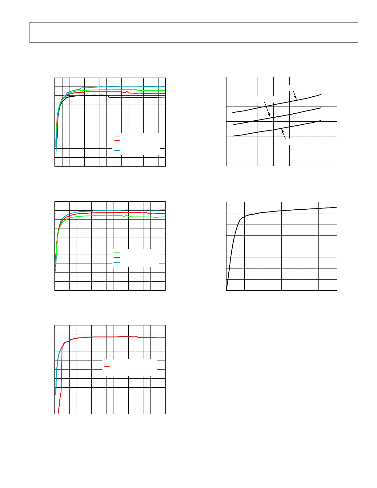
VBAT = 3.6 V, TA = 25°C, unless otherwise noted. Inductor = LPS4012-472MLB. Schottky rectifier = MBR140SFT1G.
90
85
80
75
70
65
60
EFFICIE NCY (%)
55
50
45
40
024681012141618202224262830
BACKLIGHT CURRENT (mA)
6 LEDs, VBAT = 3. 0V
6 LEDs, VBAT = 3. 6V
6 LEDs, VBAT = 4. 2V
6 LEDs, VBAT = 5. 5V
Figure 4. Efficiency vs. Backlight Current (6 LEDs)
07780-004
48
40
TEMP = +25°C
32
24
16
8
STANDBY SUPPLY CURRENT (µA)
0
2.5 3.0 3.5 4.0 4.5 5.0 5.5 6.0
TEMP = –40°C
TEMP = +85°C
VBAT (V)
Figure 7. Standby Supply Current vs. VBAT
7780-007
90
85
80
75
70
65
60
EFFICIE NCY (%)
55
50
45
40
024681012141618202224262830
BACKLIGHT CURRENT (mA)
6 LEDs, VBAT = 3. 6V
5 LEDs, VBAT = 3. 6V
4 LEDs, VBAT = 3. 6V
Figure 5. Efficiency vs. Backlight Current (4, 5, and 6 LEDs)
90
85
80
75
70
65
60
EFFICIE NCY (%)
55
50
45
40
024681012141618202224262830
BACKLIGHT CURRENT (mA)
6 LEDs, VBAT = 4.2V
6 LEDs, VBAT = 4.2V,
AUTOLOAD-ENABLED
Figure 6. Efficiency vs. Backlight Current (Autoload On/Off)
16
14
12
10
8
6
4
2
AUX LED FULL -SCALE SINK CURRENT (mA)
0
0 0.5 1.0 1.5 2.0 2.5 3.0
07780-005
AUX LED PIN VO LTAGE (V )
07780-008
Figure 8. Typical Auxiliary LED Pin (LED0, LED1, LED2), Full-Scale
Sink Current vs. Applied Pin Voltage
07780-006
Rev. 0 | Page 7 of 28
ADP5501
SW
1
INDUCTOR CURRENT
2
BST
BL_SNK
3
4
CH1 20.0V
CH3 10.0V
CH2 500mA
CH4 1.0V
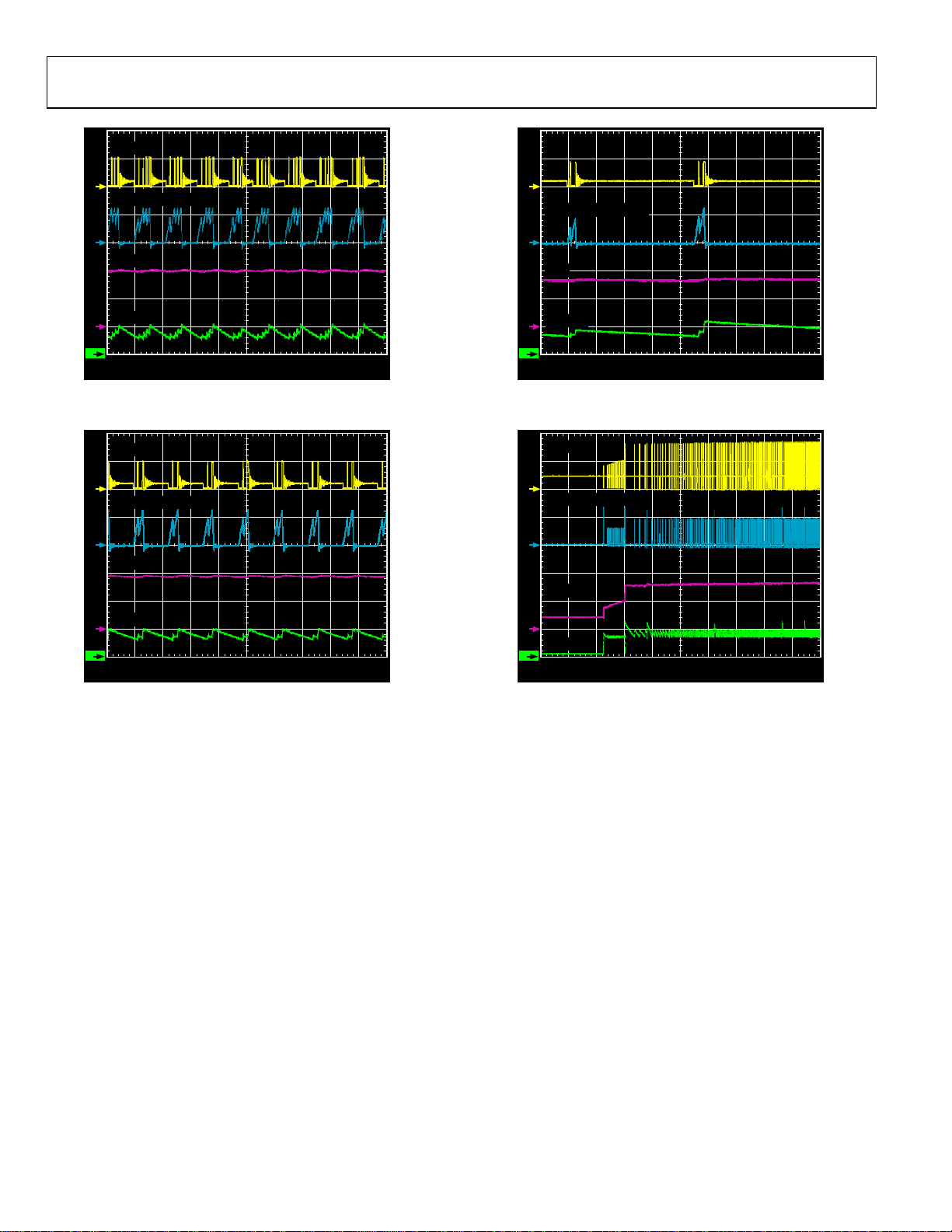
Figure 9. Boost Operation (Backlight = 30 mA)
SW
1
INDUCTOR CURRENT
2
BST
TIME (4µs/DIV)
SW
1
INDUCTOR CURRENT
2
BST
BL_SNK
3
0907780-0
4
CH1 20.0V
CH3 10.0V
CH2 500mA
CH4 1.0V
TIME (4µs/DIV)
07780-011
Figure 11. Boost Operation (Backlight = 2 mA)
SW
1
INDUCTOR CURRENT
2
BST
BL_SNK
3
4
CH1 20.0V
CH3 10.0V
CH2 500mA
CH4 1.0V
Figure 10. Boost Operation (Backlight = 15 mA)
TIME (4µs/DIV)
07780-010
3
4
BL_SNK
CH1 10.0V
CH3 10.0V
CH2 500mA
CH4 1.0V
TIME (1ms/DIV)
Figure 12. Boost Startup
07780-012
Rev. 0 | Page 8 of 28
ADP5501
2
V
THEORY OF OPERATION
.7V TO 5.5
1µF
4.7µH
1µF
PGND
VBAT
VDDIO
CAP_OUT
1µF
SCL
SDA
INT
RST
1
21
16
20
5
4
3
15
SW
2
EN
POR
BIAS/CLOCK
INTERFACE
GND19GND24GND
18
BOOST
CONTROL
IN
LDO
OUT
2.7V
6NC7NC8NC9NC10NC11
OVPI-LIMIT
ADP5501
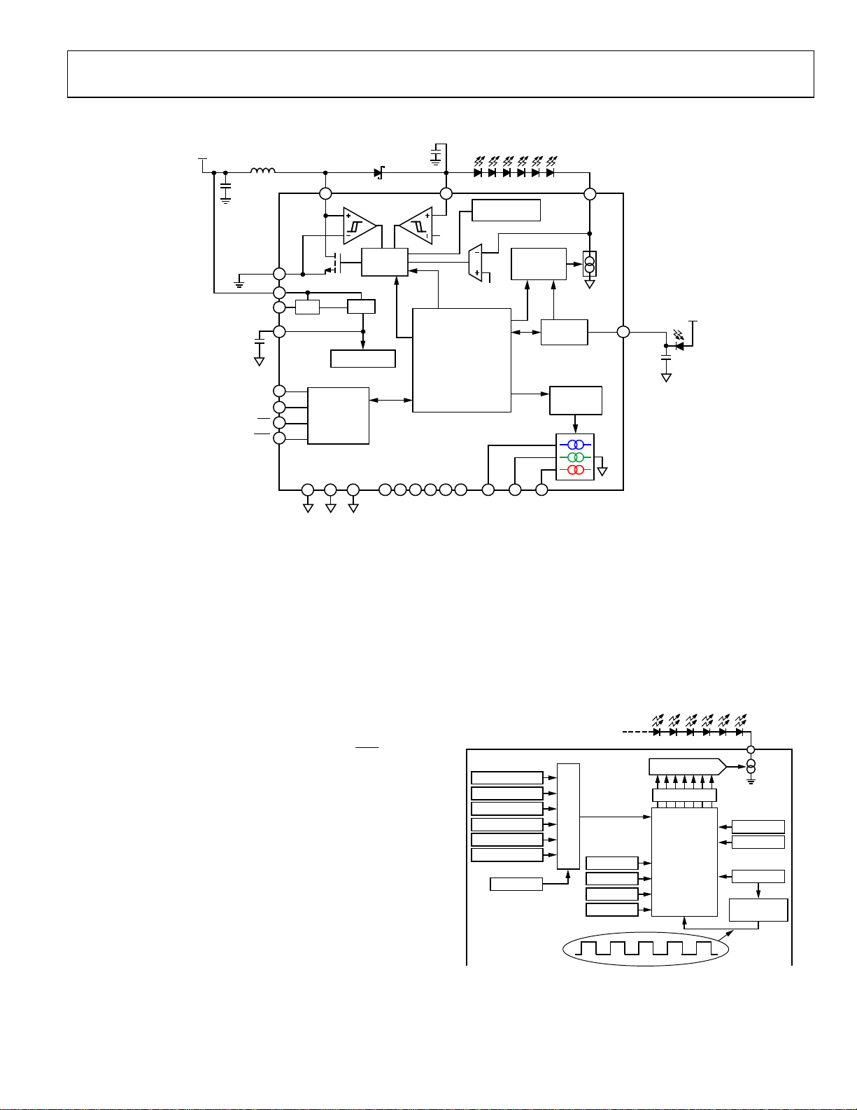
Figure 13. Internal Block Diagram
The ADP5501 is an autonomous backlight white LED driver
with programmable current and ambient light sensor input. It is
ideal for cellular phone designs and other portable devices,
where programmable and automated light output is needed. Its
versatility makes it ideal for media-enabled mobile devices.
Programmable fade-in, fade-out, dim, and off timers provide
the backlight with excellent flexibility and control features.
Using an external photodiode, the ADP5501 can perform
ambient light sensing and adjust the backlight brightness
according to varying lighting conditions.
Programmable fading is also available for the three LED sinks.
Once programmed through its I
ADP5501 can run autonomously. An interrupt line (
2
C-compatible interface, the
INT
) is
available to alert an external microprocessor of the status of its
ambient light sensor comparator states, current limit, thermal
overload, and overvoltage conditions.
BACKLIGHT DRIVE CONTROL
White LEDs are common in backlighting the displays of
modern portable devices such as cell phones. White LEDs
require a high forward voltage, V
conduct current and emit light. Display panels, depending on
their size, can be backlit with single or multiple white LEDs. In
panels that require multiple LEDs, the LEDs are commonly
connected in a series string to achieve uniform brightness in
each LED by passing a common current through all of them.
The LED string, however, needs to be biased with a voltage
greater than the sum of each LED V
(typically, 3.5 V), before they
F
before it can conduct.
F
BST BL_SNK
22
27V
STATE MACHINE
REGISTER MAP
INTERRUPT/RESET
CONTROL
FB
NC
THERMAL
PROTECTION
0.65V
13
LED1
LED2
To achieve this high voltage, the ADP5501 contains a nonsynchronous boost device capable of driving an LED string with an
OVP limited to 24.5 V(minimum). For detailed information
about the boost device, see the Applications Information
section. With sufficient forward voltage created, the ADP5501
controls the current (and thus the brightness) of the LED string
via an adjustable internal current sink. An internal state
machine, in conjunction with programmable timers, dynamically
adjusts the current sink between 0 mA and 30 mA to achieve
impressive backlight control features.
DAYLIGHT_MAX
DAYLIGHT_DIM
OFFICE_MAX
OFFICE_DIM
DARK_MAX
DARK_DIM
BL_LVL
23
BACKLIGHT
CURRENT
CONTROL
LIGHT
SENSOR
LED
CURRENT
CONTRO L
14
12
LED0
MUX
17
BST
BL_OFFT
BL_DIMT
BL_FI
BL_FO
CMP_IN
Figure 14. Backlight Brightness Control
VBAT
100nF
BL_VALUE
COUNTERS
AND
CONTROL
LOGIC
07780-013
BL_SNK
BL_EN
DIM_EN
BL_LAW
CLOCK
GENERATOR
07780-014
Rev. 0 | Page 9 of 28
 Loading...