Fast Charge Battery Manager with Power
Path and USB Compatibility
ADP5065
Rev. B
Information furnished by Analog Devices is believed to be accurate and reliable. However, no
Trademarks and registered trademarks are the property of their respective owners.
Fax: 781.461.3113 ©2011–2012 Analog Devices, Inc. All rights reserved.
V_WEAK_SET AGND
PGNDx
IIN_EXT
TRK_EXT
SCL
SDA
SYS_ON_OK
CHARGER
CONTROL
BLOCK
3MHz
BUCK
CFILT
VBUS
AC
OR
USB
VINx
PGNDx
ISO_Sx
ISO_Bx
BAT_SNS
THR
SWx
INDUCTOR
SYSTEM
+
Li-Ion
ADP5065
09370-001
Data Sheet
FEATURES
3 MHz switch mode charger
1.25 A charge current from dedicated charger
Up to 680 mA charging current from 500 mA USB host
Operating input voltage from 4.0 V up to 5.5 V
Tolerant input voltage −0.5 V to +20 V (USB VBUS)
Dead battery isolation FET between battery and
charger output
Battery thermistor input with automatic charger shutdown
for when battery temperature exceeds limits
Compliant with the JEITA Li-Ion battery charging
temperature specification
SYS_EN_OK flag to hold off system turn-on until battery is at
minimum required level for guaranteed system startup
due to minimum battery voltage and/or minimum battery
charge level requirements
EOC programming with C/20, C/10 and specific current level
selection
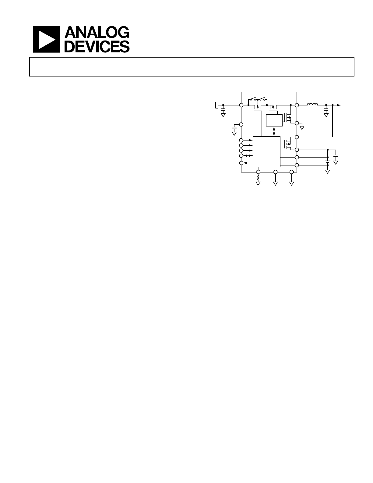
FUNCTIONAL BLOCK DIAGRAM
Figure 1.
APPLICATIONS
Digital still cameras
Digital video cameras
Single cell Li-Ion portable equipment
PDA, audio, GPS devices
Mobile phones
GENERAL DESCRIPTION
The ADP5065 charger is fully compliant with the USB 2.0,
USB 3.0, and USB Battery Charging Specification 1.1 and
enables charging via the mini USB VBUS pin from a wall
charger, car charger, or USB host port.
The ADP5065 operates from a 4 V to 5.5 V input voltage range
but is tolerant of voltages of up to 20 V. Th is alleviates the
concerns about the USB bus spiking during disconnect or
connect scenarios.
The ADP5065 also features an internal FET between the dc-todc charger output and the battery. This permits battery isolation
and, hence, system powering under a dead battery or no battery
scenario, which allows for immediate system function on
connection to a USB power supply.
Based on the type of USB source, which is detected by an external
USB detection chip, the ADP5065 can be set to apply the correct
current limit for optimal charging and USB compliance.
The ADP5065 comes in a very small and low profile 20-lead
WLCSP (0.5 mm pitch spacing) package.
The overall solution requires only five small, low profile external
components consisting of four ceramic capacitors (one of which
is the battery filter capacitor), one multilayer inductor. In addition
to these components, there is one optional dead battery situation
default setting resistor. This configuration enables a very small
PCB area to provide an integrated and performance enhancing
solution to USB battery charging and power rail provision.
responsibility is assumed by Analog Devices for its use, nor for any infringements of patents or other
rights of third parties that may result from its use. Specifications subject to change without notice. No
license is granted by implication or otherwise under any patent or patent rights of Analog Devices.
One Technology Way, P.O. Box 9106, Norwood, MA 02062-9106, U.S.A.
Tel: 781.329.4700
www.analog.com

ADP5065 Data Sheet
TABLE OF CONTENTS
Features .............................................................................................. 1
Applications ....................................................................................... 1
Functional Block Diagram .............................................................. 1
General Description ......................................................................... 1
Revision History ............................................................................... 2
Specifications ..................................................................................... 3
Recommended Input and Output Capacitance ........................ 5
I2C-Compatible Interface Timing Specifications ..................... 6
Absolute Maximum Ratings ....................................................... 7
Thermal Resistance ...................................................................... 7
ESD Caution .................................................................................. 7
Pin Configuration and Function Descriptions ............................. 8
Typical Performance Characteristics ............................................. 9
Temperature Characteristics ..................................................... 11
Typical Waveforms ..................................................................... 13
Theory of Operation ...................................................................... 15
Introduction ................................................................................ 15
Charger Modes............................................................................ 17
Thermal Management ............................................................... 19
Battery Isolation FET ................................................................. 19
Battery Detection ....................................................................... 20
Battery Pack Temperature Sensing .......................................... 22
External Resistor for V_WEAK_SET ...................................... 23
I2C Interface ................................................................................ 24
Charger Operational Flowchart ............................................... 25
I2C Register Map ......................................................................... 26
Register Bit Descriptions ........................................................... 27
Applications Information .............................................................. 33
External Components ................................................................ 33
PCB Layout Guidelines .................................................................. 35
Power Dissipation and Thermal Considerations ....................... 37
Charger Power Dissipation ....................................................... 37
Junction Temperature ................................................................ 38
Factory-Programmable Options .................................................. 39
Packaging and Ordering Information ......................................... 40
Outline Dimensions ................................................................... 40
Ordering Guide .......................................................................... 40
REVISION HISTORY
4/12—Re v.A to Rev. B
Changes to Features Section and General Description Section ........ 1
Changes to Table 1 ............................................................................ 3
Changes to VIN1, VIN2 to PGND1, PGND2 Parameter, Tab l e 4 ... 7
Changes to Introduction Section .................................................. 15
11/11—Rev. 0 to Rev. A
Changes to Figure 10 ...................................................................... 10
Changes to Figure 17 and Figure 18 ............................................. 11
Changes to Figure 41 ...................................................................... 36
10/11—Revision 0: Initial Version
Rev. B | Page 2 of 40

Data Sheet ADP5065
Parameter
Symbol
Min
Typ
Max
Unit
Test Conditions/Comments
GENERAL PARAMETERS
Undervoltage Lockout
V
2.25
2.35
2.45 V Falling threshold, higher of V
and V
Total Input Current
I
86
92
100
mA
Nominal USB initialized current level1
150
mA
USB super speed
300
mA
USB enumerated current level (specification
for China)
900
mA
Dedicated charger input
1500
mA
Dedicated wall charger
VINx
I
15 mA
No battery, no ISO_Sx load, switching 3 MHz
SWxPin Leakage Current
−I
2 µA
V
= 0 V, TJ = −40°C to +85°C
CHARGING PARAMETERS
Fast Charge Current, CC Mode
I
1250 mA
V
> V
+ V
1, 2
Fast Charge Current Accuracy
I
−7 +5 % Tj = 25°C, I
= 550 mA to 1250 mA
−8 +8 % I
= 550 mA to 1150 mA, fast charge current
−17 +8 % I
= 1250 mA, Tj = 0°C to isothermal regulation
limit (typically Tj = 115°C)
Weak Charge Current
I
I
+ 20
mA
When V
< V
< V
1, 3
Dead Battery
Trickle to Weak Charge Threshold
V
2.4
2.5
2.6 V On BAT_SNS1
Trickle to Weak Charge Threshold
ΔV
90 mV
Weak Battery
Weak to Fast Charge Threshold
V
2.9
3.0
3.1 V On BAT_SNS
1, 3
Battery Termination Voltage
V
4.158
4.200
4.242
V
On BAT_SNS, TJ = 0°C to 115°C1
Battery Overvoltage Threshold
V
V
− 0.15
V Relative to CFILT voltage, BAT_SNS rising
Charge Complete Current
I
52.5 mA
V
= V
1
Accuracy
−55 +55 % I
= 32.5 mA, TJ = 0°C to 115°C
Recharge Voltage Differential
V
260 mV
Relative to V
, BAT_SNS falling1
Switching Frequency
f
2.8 3 3.2
MHz
Maximum Duty Cycle
D
93 %
Regulated System Voltage
V
ISO_STRK
3.21
3.3
3.39 V V
BAT_SNS
< V
TRK_DEAD
, trickle charging mode
PMOS On Resistance
R
220
285
mΩ
SPECIFICATIONS
−40°C < TJ < 125°C, VIN = 5.0 V, V
4.7 µF, L
= 1 µH, all registers are at default values, unless otherwise noted.
OUT
Table 1.
> 3.0 V, V
ISO_S
HOT
< V
THR
< V
COLD
, V
BAT_ SNS
= 3.6 V, C
= 2.2 µF, C
VIN
= 22 µF, C
DCDC
= 22 µF, C
BAT
CF ILT
=
UVLO
50 100 150 mV Hysteresis, higher of V
VIN
CFILT
and V
460 475 500 mA USB enumerated current level
Current Consumption
QVIN
Battery, Standby I
(Battery Voltage > V
TRK_DEAD
)
0.22 2 µA TJ = −40°C to +85°C
QISO_B
OUT
CHG
CHG(TOL)
CHG
VIN
CFILT
BAT_SNS
CCDROP
CHG
accuracy is guaranteed at temperatures from
= 0°C to isothermal regulation limit (typically
T
j
= 115°C)
T
j
CHG
Trickle Charge Current
1, 2
I
16 20 25 mA
TRK_DEAD
CHG_WEAK
TRK_DEA D
TRK_DEAD
CHG
TRK_DEA D
BAT_SNS
WEAK
Hysteresis
CFILT
BAT_SNS
BAT_SNS
rising
Weak Battery Threshold Hysteresis ΔV
Battery Termination Voltage Accuracy −0.3 +0.3 % On BAT_SNS, TJ = 25°C, I
Charge Complete Current Threshold
−35 +35 % I
Battery Node Short Threshold Voltage1 V
CHARGER DC-to-DC CONVERTER
Peak Inductor Current I
Load Regulation 5 mV/A
DC-to-DC Power
NMOS On Resistance R
WEAK
90 mV
WEAK
TRM
= 52.5 mA1
END
BATOV
END
−25 +25 % I
RCH
2.3 2.4 2.5 V
BAT_S HR
SWCHG
MAX
1500 1750 2000 mA
L(PK)
DS(ON)P
160 210 mΩ
DS(ON)N
CFILT
Rev. B | Page 3 of 40
BAT_SNS
END
END
END
TRM
= 72.5 mA or 92.5 mA, TJ = 0°C to 115°C
= 52.5 mA, TJ = 0°C to 115°C
TRM

ADP5065 Data Sheet
Parameter
Symbol
Min
Typ
Max
Unit
Test Conditions/Comments
Bump to Bump Resistance Between
R
76
115
mΩ
Includes bump resistances and battery isolation
Regulated System Voltage
V
3.15
3.3
3.45 V V
< V
, fast charging CC mode
VINx Input
High Voltage Blocking FET On
R
340
455
mΩ
IIN = 500 mA
Current, Suspend Mode
I
1.3
2.5
mA
EN_CHG = low
Input Voltage
Good Threshold
Rising
V
3.78
3.9
4.0 V
Overvoltage Threshold
V
5.35
5.42
5.5 V
Overvoltage Threshold Hysteresis
75 mV
Minimum Rise Time for VINx from
t
10
µs
Minimum Fall Time for VINx from
4 V to 0 V
t
10
µs
THERMAL CONTROL
Thermal Early Warning Temperature
T
130 °C
Thermal Shutdown Temperature
TSD 140 °C
TJ rising
Thermistor Current
10,000 NTC
I
400
μA
Thermistor Capacitance
C
100
pF
Resistance Thresholds
Cool to Cold Resistance
R
24,050
27,300
30,600
Ω
Hot Temperature Threshold
T
60 °C
No battery charging occurs
Hot to Typical Resistance
R
2990
3310
3640 Ω
Typical to Hot Resistance
R
2730
3030
3330 Ω
JEITA SPECIFICATION4
Resistance Thresholds
Cool to Cold Resistance
R
24,050
27,300
30,600
Ω
JEITA Cool Temperature
T
10 °C
Battery charging occurs at 50% of
Resistance Thresholds
Typical to Cool Resistance
R
15,200
17,800
20,400
Ω
JEITA Typical Temperature
T
°C
Normal battery charging occurs at
default/programmed levels
Resistance Thresholds
Warm to Typical Resistance
R
4710
5400
6100 Ω
Resistance Thresholds
Warm to Hot Resistance
R
2730
3030
3330 Ω
JEITA Hot Temperature
T
60 °C
No battery charging occurs
BATTERY ISOLATION FET
ISO_Bx and ISO_Sx Bumps
Battery Supplementary Threshold V
HIGH VOLTAGE BLOCKING FET
DSONISO
ISO_SFC
0 5 10 mV V
THISO
PMOS on resistance; on battery supplement
mode, V
TRK_DEA D
ISO_S[1:2]
= 0 V, V
IN
< V
BAT_SNS
ISO_B[1:2]
ISO_B
, V
SYS
= 3.6 V, I
rising
= 500 mA
ISO_B
Resistance
DSONHV
SUSPEND
VIN_OK_RISE
Falling V
3.6 3.67 V
VIN_OK_FALL
VIN_OV
VINx Transition Timing
5 V to 20 V
VIN_RISE
VIN_FALL
Isothermal Charging Temperature T
115 °C
LIM
SDL
110 °C TJ falling
THERMISTOR CONTROL
NTC_10k
100,000 NTC I
Cold Temperature Threshold T
Cold to Cool Resistance R
40 μA
NTC_100k
NTC
0 °C No battery charging occurs
NTC_COLD
COLD_FA LL
23,100 26,200 29,400 Ω
COLD_R ISE
NTC_HOT
Resistance Thresholds
HOT_FALL
HOT_RIS E
JEITA Cold Temperature T
Cold to Cool Resistance R
Cool to Typical Resistance R
Typical to Warm Resistance R
JEITA Warm Temperature T
Hot to Warm Resistance R
0 °C No battery charging occurs
JEITA_C OLD
COLD_FA LL
23,100 26,200 29,400 Ω
COLD_R ISE
JEITA_ COOL
programmed level
TYP_FALL
14,500 17,000 19,500 Ω
TYP_RISE
JEITA_TY P
WARM_FALL
WARM_RISE
JEITA_W ARM
4320 4950 5590 Ω
45 °C Battery termination voltage (V
by 100 mV
2990 3310 3640 Ω
HOT_FALL
HOT_RIS E
JEITA_H OT
Rev. B | Page 4 of 40
) is reduced
TRM

Data Sheet ADP5065
Parameter
Symbol
Min
Typ
Max
Unit
Test Conditions/Comments
Sink Current
I
13
20
34
mA
Source Current
I
7
10
13
mA
Battery Threshold
Low
V
1.8
1.9
2.0 V
No Battery Threshold
V
3.3 V
V
≥ 3.7 V, valid after charge complete (see
Figure 38)
Figure 38)
Trickle Charge Timer
t
60 min
Charge Complete Timer
t
END
7.5 min
V
BAT_SNS
= V
TRM
, I
CHG
< I
END
Deglitch Timer
tDG 31 ms
Applies to V
, V
, I
, V
, V
Safety Timer
t
36
40
44
min
Maximum Logic Low Input Voltage
VIL
0.5 V Applies to SCL, SDA, TRK_EXT, IIN_EXT
Pull-Down Resistance
215
350
610
kΩ
Applies to TRK_EXT, IIN_EXT
BATTERY DETECTION
SINK
SOUR CE
BATL
High V
3.4 V
BATH
NOBAT
TRM
3.0 V V
Battery Detection Timer t
333 ms
BATOK
< 3.7 V, valid after charge complete (see
TRM
TIMERS
Start Charging Delay Timer t
Fast Charge Timer t
1 sec
START
TRK
600 min
CHG
TRK
RCH
END
DEAD
Watchdog Timer1 tWD 32 sec
SAFE
Battery Node Short Timer1 t
30 sec
BAT_S HR
LOGIC INPUTS
Maximum Voltage on Digital Inputs V
5.5 V
DIN_MAX
Minimum Logic High Input Voltage VIH 1.2 V Applies to SCL, SDA, TRK_EXT, IIN_EXT
1
These values are programmable via I2C. Values are given with default register values.
2
The output current during charging can be limited by I
3
Programmable via external resistor programming, if required.
4
JEITA can be enabled or disabled in I2C.
or by the isothermal charging mode.
BUS
RECOMMENDED INPUT AND OUTPUT CAPACITANCE
Table 2.
Parameter Min Typ Max Unit Test Conditions/Comments
CAPACITANCE
VINx Capacitance 1.0 µF Effective capacitance
CFILT Pin Total External Capacitance 2.0 4.7 5.0 μF Effective capacitance
ISO_Sx Pin Total Capacitance 10 50 µF Effective capacitance
ISO_Bx Pin Total Capacitance 10 µF Effective capacitance
VIN_OK
Rev. B | Page 5 of 40
ADP5065 Data Sheet
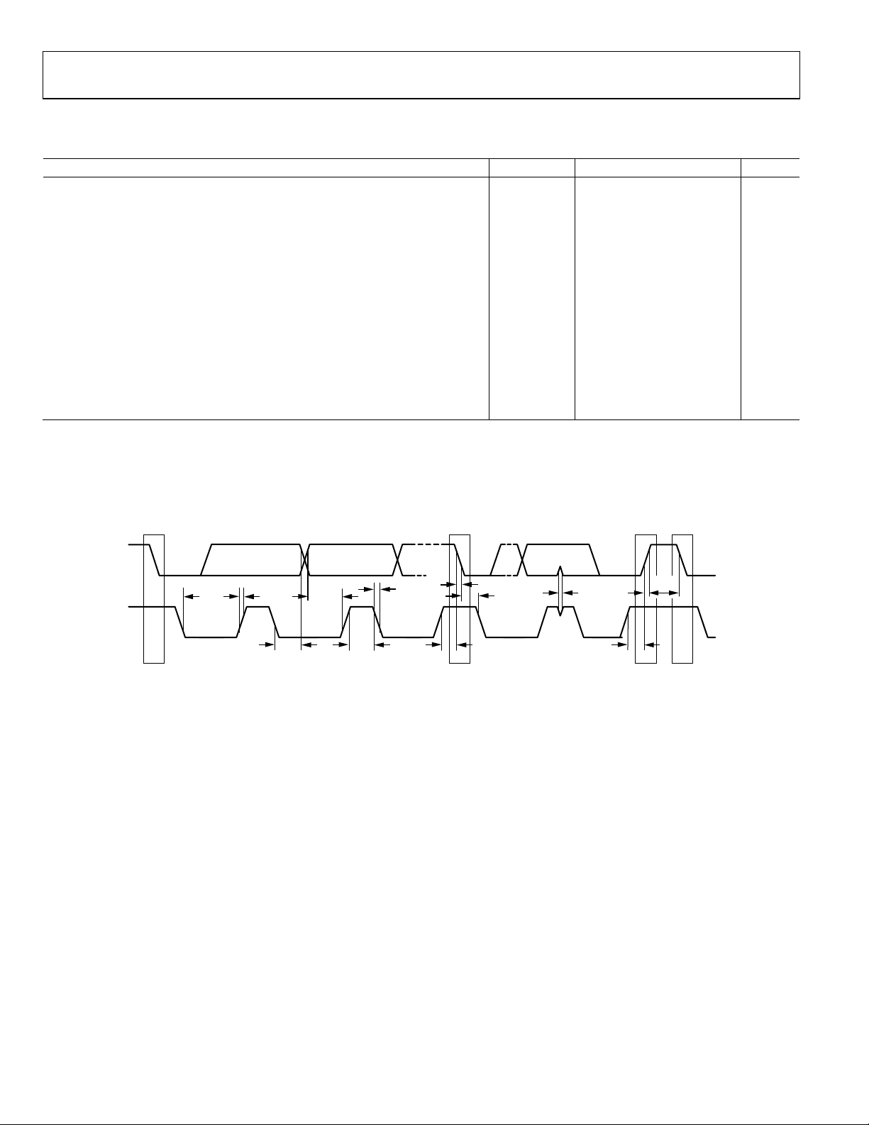
I2C-COMPATIBLE INTERFACE2
S = START CONDITION
Sr = REPEATED S TART CONDITION
P = STOP CONDITION
t
LOW
t
SU,DAT
t
R
t
HD,DAT
t
SU,STA
t
SU,STO
t
SPtR
t
BUF
t
HIGH
S Sr P S
SDA
SCL
t
F
t
HD,STA
t
F
09370-002
I2C-COMPATIBLE INTERFACE TIMING SPECIFICATIONS
Table 3.
Parameter1 Symbol Min Typ Max Unit
Capacitive Load, Each Bus Line CS 400 pF
SCL Clock Frequency f
SCL High Time t
SCL Low Time t
Data Setup Time t
Data Hold Time t
Setup Time for Repeated Start t
Hold Time for Start/Repeated Start t
Bus Free Time Between a Stop and a Start Condition t
Setup Time for Stop Condition t
SCL
HIGH
LOW
SU DAT
0 0.9 µs
HDDAT
SU STA
HD STA
BUF
SUSTO
Rise Time of SCL/SDA tR 20 300 ns
Fall Time of SCL/SDA tF 20
Pulse Width of Suppressed Spike t
1
Guaranteed by design.
2
A master device must provide a hold time of at least 300 ns for the SDA signal to bridge the undefined region of the falling edge of SCL. See Figure 2, the I2C timing
diagram.
SP
Timing Diagram
400 kHz
0.6 µs
1.3 µs
100 ns
0.6 µs
0.6 µs
1.3 µs
0.6 µs
300 ns
0 50 ns
2
Figure 2. I
C Timing Diagram
Rev. B | Page 6 of 40
Data Sheet ADP5065
VIN1, VIN2 to PGND1, PGND2
−0.5 V to +20 V
Stresses a bove those l isted under Absolute Maximum Ratings
may cause permanent damage to the device. This is a stress
rating only; functional operation of the device at these or any
other conditions above those indicated in the operational
section of this specification is not implied. Exposure to absolute
maximum rating conditions for extended periods may affect
device reliability.
ABSOLUTE MAXIMUM RATINGS
Table 4.
Parameter Rating
All Other Pins to AGND −0.3 V to +6 V
Continuous Drain Current, Battery Supple-
mentary Mode, from ISO_Bx to ISO_Sx
TJ ≤ 85°C 2.2 A
TJ = 125°C 1.1 A
Storage Temperature Range −65°C to +150°C
Operating Junction Temperature Range −40°C to +125°C
Soldering Conditions JEDEC J-STD-020
THERMAL RESISTANCE
θJA is specified for the worst-case conditions, that is, a device
soldered in a circuit board for surface-mount packages.
Table 5. Thermal Resistance
Package Type θJA θJC θJB Unit
20-Lead WLC SP1 46.8 0.7 9.2 °C/W
1
5 × 4 array, 0.5 mm pitch (2.75 mm × 2.08 mm); based on a JEDEC, 2S2P,
4-layer board with 0 m/sec airflow.
Maximum Power Dissipation
The maximum safe power dissipation in the ADP5065 package
is limited by the associated rise in junction temperature (T
) on
J
the die. At approximately 150°C, which is the glass transition
temperature, the plastic changes its properties. Even temporarily
exceeding this temperature limit may change the stresses that
the package exerts on the die, permanently shifting the parametric performance of the ADP5065. Exceeding a junction
temperature of 175°C for an extended period of time can result
in changes in the silicon devices that potentially cause failure.
ESD CAUTION
Rev. B | Page 7 of 40
ADP5065 Data Sheet
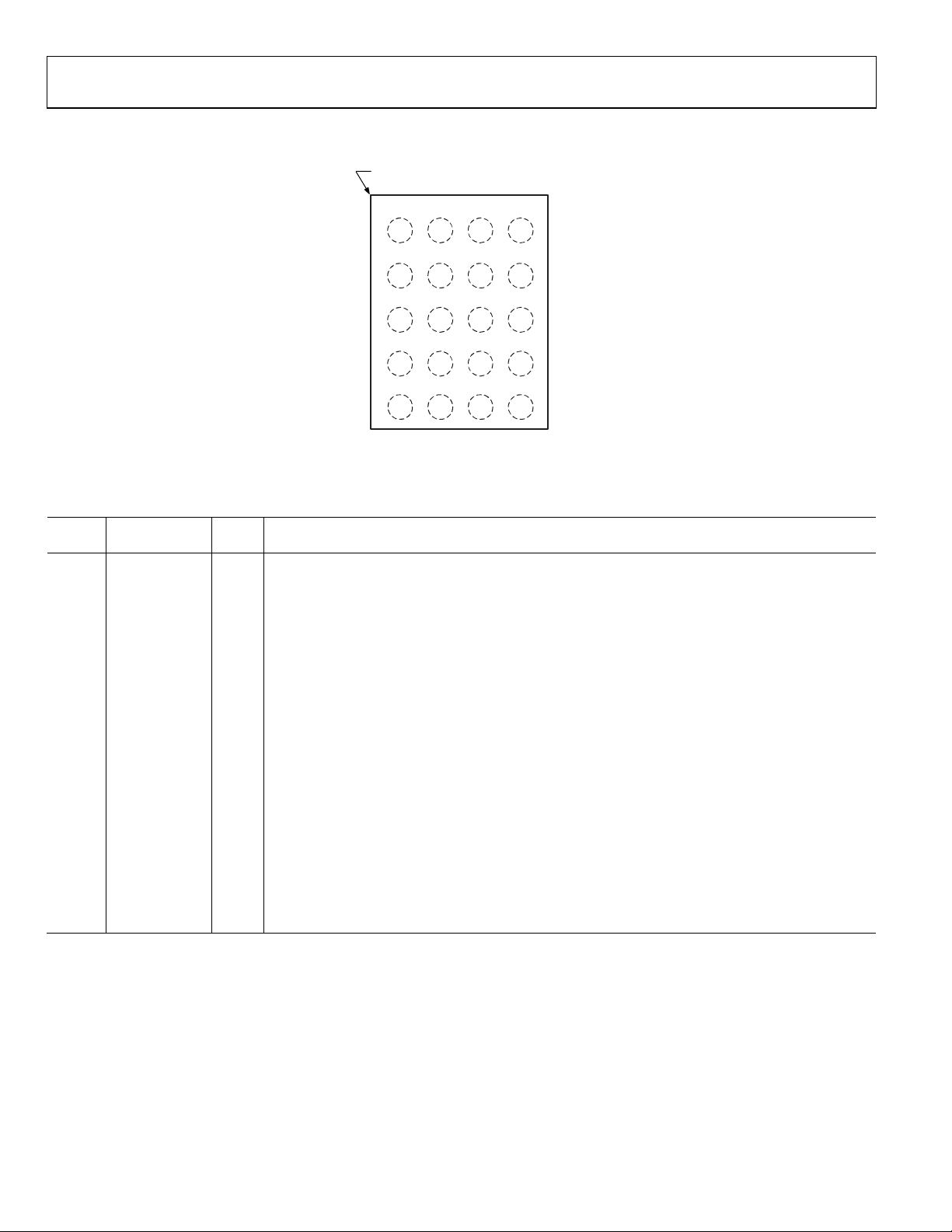
TOP VIEW
(BALL SI DE DOWN)
Not to Scale
1
A
B
C
D
E
2 3 4
BALL A1
CORNER
V_WEAK_SET
SDA
BAT_SNS
VIN1
THR
ISO_B1
ISO_S1
SW1
IIN_EXT
ISO_B2
ISO_S2
PGND1
SCL
TRK_EXT
AGND
SYS_ON_OK
VIN2 SW2 PGND2
CFILT
09370-003
Pin
B1
SDA
I/O
I2C-Compatible Interface Serial Data.
A3
THR I Battery Pack Thermistor Connection. If not used, connect a dummy 10 kΩ resistor from THR to GND.
PIN CONFIGURATION AND FUNCTION DESCRIPTIONS
Table 6. Pin Function Descriptions
No. Mnemonic Typ e1 Description
D3, E3 SW1, SW2 I/O DC-to-DC Converter Inductor Connection. These pins are high current outputs when in charging mode.
D1, E1 VIN1, VIN2 I/O Power Connection to USB VBUS. These pins are high current inputs when in charging mode.
D4, E4 PGND1,
C2 AGND G Analog Ground.
E2 CF ILT I/O 4.7 μF Filter Capacitor Connection. This pin is a high current input/output when in charging mode.
C3, C4 ISO_S1, ISO_S2 I/O Charger Supply Side Input to Internal Isolation FET/Battery Current Regulation FET.
B3, B4 ISO_B1,
A2 SCL I I2C-Compatible Interface Serial Clock.
A4 IIN_EXT I Set Input Current Limit. This pin sets the input current limit directly. When IIN_EXT = low or high-Z, the
B2 TRK_EXT I Enable Trickle Charge Function. When TRK_EXT = low or high-Z, the trickle charge is enabled. When
C1 B AT_SNS I Battery Voltage Sense Pin.
D2 SYS_ON_OK O Battery Okay Open-Drain Output Flag. Active low. This pin enables the system when the battery
A1 V_WEAK_SET I/O External Resistor Setting Pin for V_WEAK threshold. The use of this pin is optional. When not in use,
1
I is input, O is output, I/O is input/output, and G is ground.
PGND2
ISO_B2
Figure 3. Pin Configuration
G Charger Power Ground. These pins are high current inputs when in charging mode.
I/O Battery Supply Side Input to Internal Isolation FET/Battery Current Regulation FET.
input limit is 100 mA. When IIN_EXT = high, the input limit is 500 mA.
TRK_EXT = high, the trickle charge is disabled.
reaches V
WEAK
.
connect to GND.
Rev. B | Page 8 of 40
Data Sheet ADP5065
100
0
10
20
30
40
50
60
70
90
80
2.5 2.9 3.3 3.7 4.1 4.5
EFFICIENCY (%)
BATTERY VOLTAGE (V)
VIN INPUT LIMIT 100mA
V
IN
INPUT LIMIT 500mA
09370-004
0.001 0.01 0.1 1
SYSTEM VOLTAGE (V)
SYSTEM OUTPUT CURRENT ( A)
3.25
3.26
3.27
3.28
3.29
3.30
3.31
3.32
3.33
3.34
3.35
09370-005
700
0
100
200
300
400
500
600
2.7 3.0 3.3 3.6 3.9 4.2
BATTERY CHARG E CURRE NT (mA)
BATTERY VOLTAGE (V)
09370-006
0.01 0.1 1
SYSTEM OUTPUT CURRENT ( A)
100
0
10
20
30
40
50
60
70
90
80
EFFICI E NCY ( %)
09370-007
2.7 3.0 3.3 3.6 3.9 4.2
BATTERY VOLTAGE (V)
4.5
2.5
2.7
2.9
3.1
3.3
3.5
3.7
3.9
4.3
4.1
SYSTEM VOLTAGE (V)
SYSTEM VOLTAGE
BATTERY VOLTAGE
09370-008
2.7 3.0 3.3 3.6 3.9 4.2
BATTERY VOLTAGE (V)
140
0
20
40
60
80
100
120
BATTERY CHARG E CURRE NT (mA)
09370-009
TYPICAL PERFORMANCE CHARACTERISTICS
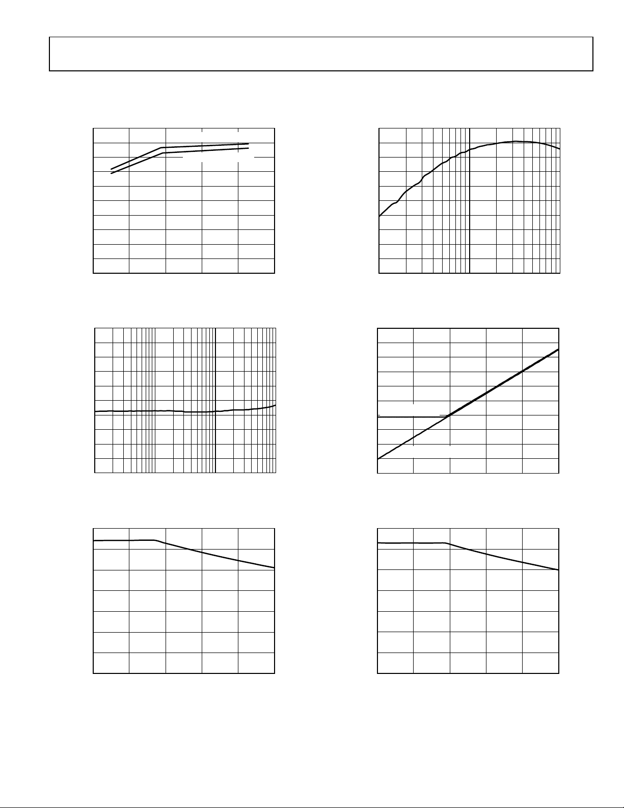
Figure 4. Battery Charger Efficiency vs. Battery Voltage, VIN = 5.0 V
Figure 5. System Voltage Regulation vs. Output Current, VIN = 5.0 V
Figure 7. System Voltage Efficiency vs. Output Current, VIN = 5.0 V
Figure 8. System Voltage vs. Battery Voltage, VIN = 5.0 V, ILIM = 100 mA
Figure 6. USB Compliant Charge Current vs. Battery Voltage,
V
= 5.0 V, ILIM = 500 mA
IN
Figure 9. USB Limited Battery Charge Current vs. Battery Voltage,
V
= 5.0 V, ILIM = 100 mA
IN
Rev. B | Page 9 of 40
ADP5065 Data Sheet
2.7 3.0 3.3 3.6 3.9 4.2
BATTERY VOLTAGE (V)
100
70
75
80
85
90
95
RON RESISTANCE (mΩ)
09370-010
1 2 3 4 5 6
VIN VOLTAGE (V)
1.6
1.4
1.2
1.0
0.8
0.6
0.4
0.2
0
VIN CURRENT (mA)
09370-011
0 50 100 150
CHARGE TIM E ( M inutes)
4.4
4.2
4.0
3.8
3.6
3.4
3.2
3.0
0.7
0.6
0.5
0.4
0.3
0.2
0
0.1
BATTERY VOLTAGE (V)
CURRENT (A)
V
BAT_SNS
I
ISO_B
I
VIN
09370-012
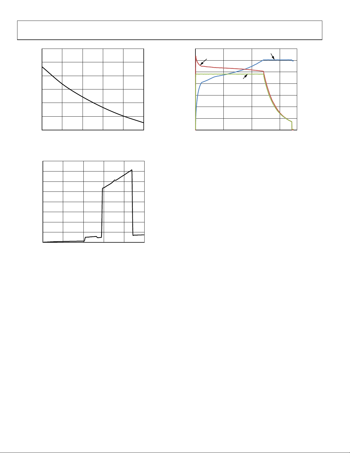
Figure 10. Battery Isolation FET Resistance vs. Battery Voltage, VIN = 5.0 V,
Load Current = 1.0 A
Figure 11. VINx Current vs. VINx Voltage, Suspend Mode (EN_CHG = 0)
Figure 12. Charge Profile, VIN = 5.0 V, ILIM = 500 mA,
Battery Capacity = 1320 mAh
Rev. B | Page 10 of 40
Data Sheet ADP5065
AMBIENT T E M P E RATURE (°C)
VIN OVERVOLTAGE PROTECTION (V)
5.25
5.30
5.35
5.40
5.45
5.50
5.55
5.60
5.65
5.70
5.75
–40 –20 0 20 40 60 80 100 120
09370-013
AMBIENT T E M P E RATURE (°C)
SYSTEM VOLTAGE (V)
–40 –20 0 20 40 60 80 100 120
3.275
3.280
3.285
3.290
3.295
3.300
3.305
3.310
3.315
09370-014
AMBIENT T E M P E RATURE (°C)
INPUT CURRENT LIMIT ( mA)
–40 –20 0 20 40 60 80 100 120
0
50
100
150
200
250
300
350
400
450
500
VIN INPUT LIMIT 100mA
V
IN
INPUT LIMIT 500mA
09370-015
AMBIENT T E M P E RATURE (°C)
V
TRM
ACCURACY (%)
–40 –20 0 20 40 60 80 100 120
–1.0
1.0
0.5
0
–0.5
V
TRM
= 3.50V
V
TRM
= 3.80V
V
TRM
= 4.20V
V
TRM
= 4.42V
09370-016
AMBIENT T E M P E RATURE (°C)
SWITCHING FREQUE NCY ( M Hz )
–40 –20 0 20 40 60 80 100 120
2.90
2.92
2.94
2.96
2.98
3.00
3.02
3.04
3.06
3.08
3.10
09370-017
AMBIENT T E M P E RATURE (°C)
CHARGE CURRENT (A)
–40 –20 0 20 40 60 80 100 120
1.00
1.01
1.02
1.03
1.04
1.05
1.06
1.07
1.08
1.09
1.10
09370-018
TEMPERATURE CHARACTERISTICS
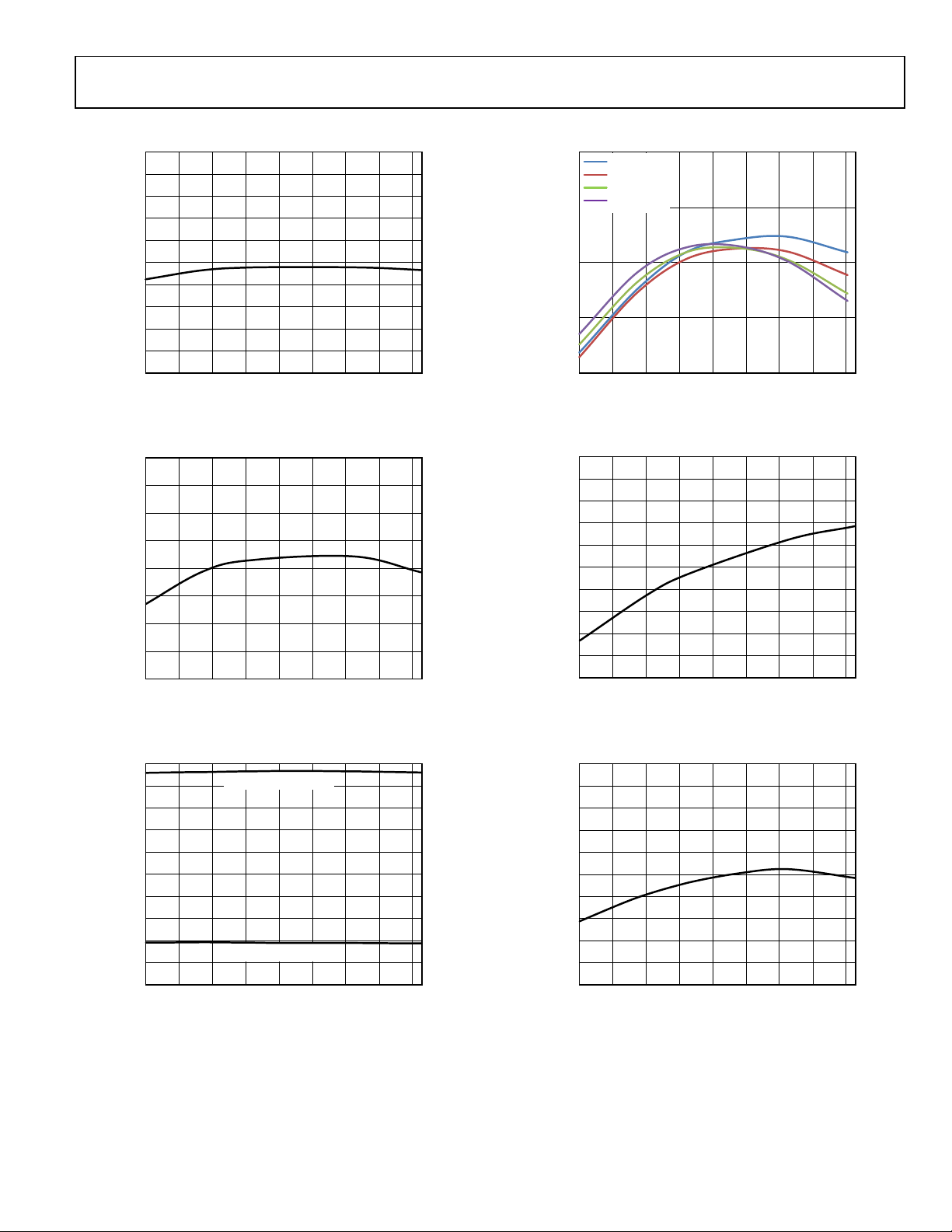
Figure 13. VINx Overvoltage Protection Rising Threshold vs. Ambient
Temperature
Figure 14. System Voltage vs. Ambient Temperature, VIN = 5.0 V, R
LOAD
= 33 Ω
Figure 16. Termination Voltage vs. Ambient Temperature, VIN = 5.0 V, V
Programming 3.50 V, 3.80 V, 4.20 V, and 4.42 V
Figure 17. Switching Frequency vs. Ambient Temperature, VIN = 5.0 V
TRM
Figure 15. Input Current Limit vs. Ambient Temperature, VIN = 5.0 V
V
= 5.0 V, V
IN
ISO_B
= 3.6 V, I
= 1050 mA
CHG
Rev. B | Page 11 of 40
Figure 18. Fast Charge Current vs. Ambient Temperature,
ADP5065 Data Sheet
AMBIENT T E M P E RATURE (°C)
BATTERY L E AKAGE CURRENT (µA)
–40 –20 0 20 40 60 80
0
0.1
0.2
0.3
0.4
0.5
0.6
0.7
0.8
0.9
1.0
V
ISO_B
= 2.7V
V
ISO_B
= 3.6V
V
ISO_B
= 4.2V
09370-019
AMBIENT T E M P E RATURE (°C)
INPUT CURRENT ( mA)
–40 –20 0 20 40 60 80
1.16
1.18
1.20
1.22
1.24
1.26
1.28
1.30
1.32
1.34
09370-020
AMBIENT T E M P E RATURE (°C)
CHARGE CURRENT (A)
0 20 40 80 12060 100
0
0.1
0.2
0.3
0.4
0.5
0.6
0.7
0.8
09370-021
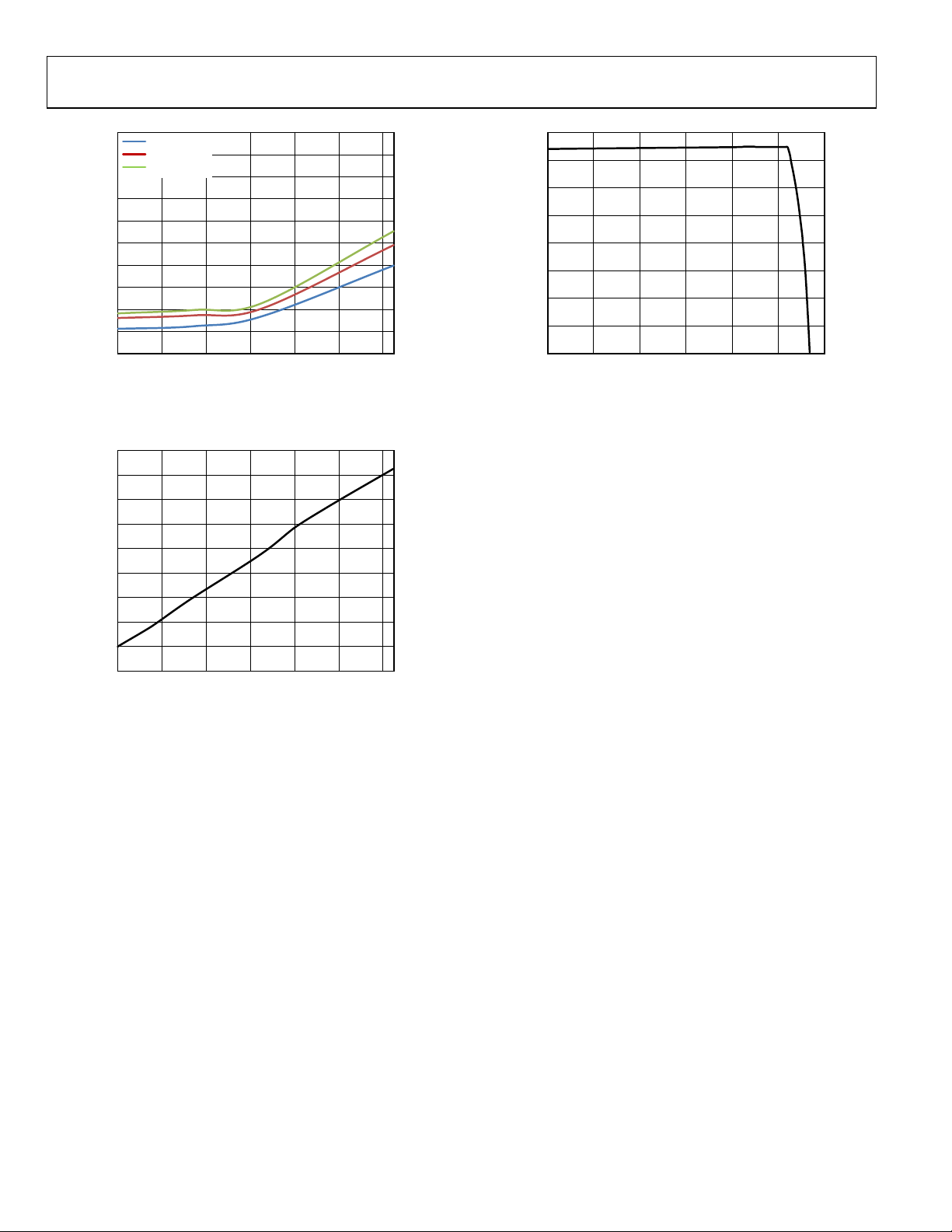
Figure 19. Battery Leakage Current vs. Ambient Temperature
Figure 20. VINx Quiescent Current vs. Temperature, VIN = 5.0 V,
Suspend Mode (EN_CHG = 0)
Figure 21. Isothermal Regulation of Charge Current vs. Ambient
Temperature, I
= 750 mA, VIN = 5.0 V, V
CHG
ISO_B
= 3.6 V
Rev. B | Page 12 of 40
 Loading...