Tiny I2C Programmable Linear Battery Charger
with Power Path and USB Mode Compatibility
ADP5061
Rev. 0
Information furnished by Analog Devices is believed to be accurate and reliable. However, no
Trademarks and registered trademarks are the property of their respective owners.
Fax: 781.461.3113 ©2012 Analog Devices, Inc. All rights reserved.
VIN
VBUS
AC OR
USB
SCL
SDA
DIG_IO1
DIG_IO2
DIG_IO3
AGND
+
Li-ion
THR
C3
47µF
C2
10nF
C1
10µF
C4
22µF
ISO_S
ISO_B
BAT_SNS
ADP5061
SYS_EN
SYSTEM
PROGRAMMABLE
ILED
VLED
CBP
CHARGER
CONTROL
BLOCK
10544-001
Data Sheet
FEATURES
2.6 mm × 2 mm WLCSP package
Fully programmable via I
Flexible digital control inputs
Up to 2.1 A current from an ac charger in LDO mode
Operating input voltage from 4.0 V to 6.7 V
Tolerant input voltage from −0.5 V to +20 V (USB VBUS)
Fully compatible with USB 3.0 and USB Battery Charging
Specification 1.2
Built-in current sensing and limiting
As low as 30 mΩ battery isolation FET between battery and
charger output
Thermal regulation prevents over heating
Compliant with JEITA 1 and JEITA 2 Li-Ion battery charging
temperature specifications
SYS_EN flag permits the system to be disabled until battery is at
minimum required level for guaranteed system start-up
2
C
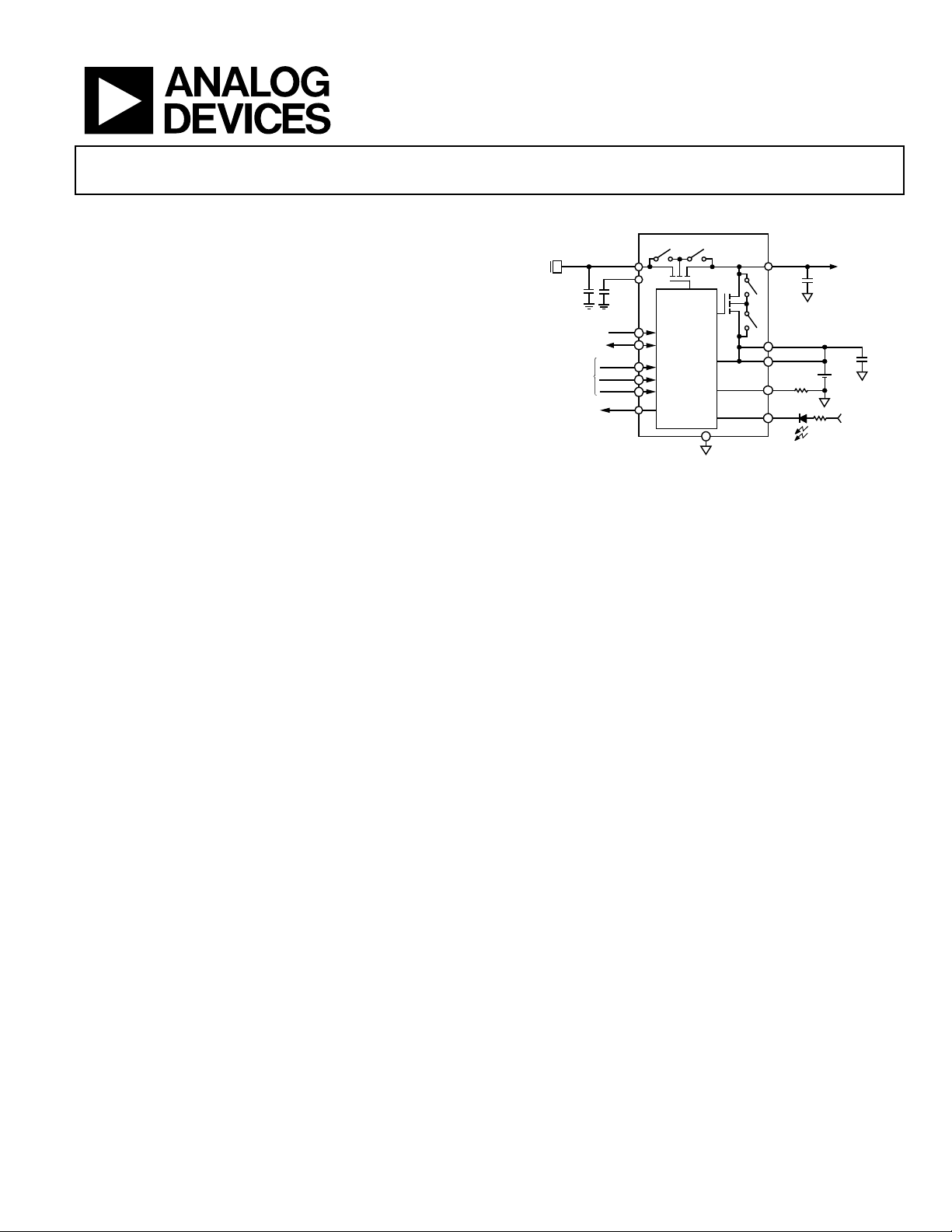
TYPICAL APPLICATION CIRCUIT
Figure 1.
APPLICATIONS
Digital still cameras
Digital video cameras
Single cell Li-Ion portable equipment
PDAs, audio, and GPS devices
Portable medical devices
Mobile phones
GENERAL DESCRIPTION
The ADP5061 charger is fully compliant with USB 3.0 and the
USB Battery Charging Specification 1.2 and enables charging
via the mini USB VBUS pin from a wall charger, car charger, or
USB host port.
The ADP5061 operates from a 4 V to 6.7 V input voltage range
but is tolerant of voltages up to 20 V. The 20 V voltage tolerance
alleviates the concerns about the USB bus spiking during disconnect or connect scenarios.
The ADP5061 features an internal FET between the linear
charger output and the battery. This permits battery isolation
and, hence, system powering under a dead battery or no battery
scenario, which allows for immediate system function on connection to a USB power supply.
Based on the type of USB source, which is detected by an external
USB detection chip, the ADP5061 can be set to apply the correct
current limit for optimal charging and USB compliance.
The ADP5061 has three factory programmable digital input/output
pins that provide maximum flexibility for different systems.
These digital input/output pins permit combinations of features
such as, input current limits, charging enable and disable,
charging current limits, and a dedicated interrupt output pin.
responsibility is assumed by Analog Devices for its use, nor for any infringements of patents or other
rights of third parties that may result from its use. Specifications subject to change without notice. No
license is granted by implication or otherwise under any patent or patent rights of Analog Dev ices.
One Technology Way, P.O. Box 9106, Norwood, MA 02062-9106, U.S.A.
Tel: 781.329.4700
www.analog.com

ADP5061 Data Sheet
TABLE OF CONTENTS
Features .............................................................................................. 1
Applications ....................................................................................... 1
Typical Application Circuit ............................................................. 1
General Description ......................................................................... 1
Revision History ............................................................................... 2
Specifications ..................................................................................... 3
Recommended Input and Output Capacitances ...................... 6
I2C-Compatible Interface Timing Specifications ..................... 6
Absolute Maximum Ratings ....................................................... 7
Thermal Resistance ...................................................................... 7
ESD Caution .................................................................................. 7
Pin Configuration and Function Descriptions ............................. 8
Typical Performance Characteristics ............................................. 9
Temperature Characteristics ..................................................... 11
Typical Waveforms ..................................................................... 13
Theory of Operation ...................................................................... 14
Summary of Operation Modes ................................................. 14
Introduction ................................................................................ 15
Charger Modes............................................................................ 17
Thermal Management ............................................................... 20
Battery Isolation FET ................................................................. 20
Battery Detection ....................................................................... 20
Battery Pack Temperature Sensing .......................................... 21
I2C Interface ................................................................................ 25
I2C Register Map ......................................................................... 26
Register Bit Descriptions ........................................................... 27
Applications Information .............................................................. 35
External Components ................................................................ 35
PCB Layout Guidelines.............................................................. 37
Power Dissipation and Thermal Considerations ....................... 38
Charger Power Dissipation ....................................................... 38
Junction Temperature ................................................................ 38
Factory Programmable Options ................................................... 39
Charger Options ......................................................................... 39
I2C Register Defaults .................................................................. 40
Digital Input and Output Options ........................................... 40
Packaging and Ordering Information ......................................... 42
Outline Dimensions ................................................................... 42
Ordering Guide .......................................................................... 42
REVISION HISTORY
6/12—Revision 0: Initial Version
Rev. 0 | Page 2 of 44

Data Sheet ADP5061
Parameter
Symbol
Min
Typ
Max
Unit
Test Conditions/Comments
Hysteresis
50
100
150
mV
Hysteresis, higher of V
and V
rising1
VINx Current Consumption
I
2 mA
Charging or LDO mode
−65 +35
mA
I
= 1000 mA to 1300 mA
Hysteresis
ΔV
100 mV
On BAT_SNS2
Termination Voltage Accuracy
−0.25
+0.25
%
On BAT_SNS, TJ = 25°C, I
= 52.5 mA2
−1.15
+1.20
%
TJ = −40°C to +125°C
Battery Short Detection Current
I
20 mA
I
= I
Charging Soft Start Current
I
185
260
365
mA
V
> V
3.3
3.5
3.7 VTRM[5:0] programming < 4.00 V
SPECIFICATIONS
−40°C < TJ < +125°C, V
C
= 10 nF, all registers at default values, unless otherwise noted.
CBP
Table 1.
= 5.0 V, V
VIN
HOT
< V
THR
< V
COLD
, V
BAT_ SNS
= 3.6 V, V
ISO_B
= V
BAT_ SNS
, C
VIN
= 10 µF, C
= 22 µF, C
ISO_S
ISO_B
= 22 µF,
GENERAL PARAMETERS
Undervoltage Lockout V
Total Input Current I
2.25 2.35 2.5 V Falling threshold, higher of V
UVLO
VIN
74 92 100 mA Nominal USB initialized current level2
LIM
VIN
BAT_SNS
and V
BAT_SNS
1
114 150 mA USB super speed
300 mA USB enumerated current level (specification for China)
425 470 500 mA USB enumerated current level
900 mA Dedicated charger input
1500 mA Dedicated wall charger
QVIN
I
Battery Current Consumption I
5 µA Standby, includes ISO_Sx pin leakage, V
280 450 µA DIS_IC1 = high, V
QVIN_D IS
20 µA LDO mode, V
QBATT
= −40°C to +85°C
T
J
ISO_S
ISO_B
> V
< VINx < 5.5 V
BAT_SNS
= 0 V,
VIN
0.5 0.9 mA Standby, battery monitor active
CHARGER
Fast Charge Current CC Mode I
Fast Charge Current Accuracy −40 +30 mA I
−50 +30 mA I
Trickle Charge Current2 I
Weak Charge Current
2, 3
I
715 750 775 mA V
CHG
16 20 25 mA
TRK_DEAD
CHG_WEAK
I
TRK_DEAD
+ I
mA
CHG
= 3.9 V; fast charge current accuracy is
ISO_B
guaranteed at temperatures from T
J
isothermal regulation limit (typically T
= 50 mA to 550 mA
CHG
= 600 mA to 950 mA
CHG
CHG
= −40°C to
= +115°C)
J
Trickle to Weak Charge Threshold
Dead Battery V
2.4 2.5 2.6 V V
TRK_DEA D
TRK_DEAD
TRK_DEA D
< V
BAT_SNS
< V
WEAK
2, 4
Weak Battery Threshold
Weak to Fast Charge Threshold V
ΔV
Battery Termination Voltage V
2.89 3.0 3.11 V On BAT_SNS
WEAK
100 mV
WEAK
4.200 V
TRM
2, 4
END
−0.96 +0.89 % TJ = 0°C to 115°C2
2, 3
Battery Overvoltage Threshold V
Charge Complete Current I
Charging Complete Current Threshold
Accuracy
59 123 I
Recharge Voltage Differential V
Battery Node Short Threshold Voltage2 V
Charging Start Voltage Limit V
Charging Soft Start Timer t
BATTERY ISOLATION FET
Bump to Bump Resistance Between
ISO_Sx and ISO_Bx
Regulated System Voltage: V
Battery Supplementary Threshold V
Low V
BAT
VIN −
BATOV
V Relative to VINx voltage, BAT_SNS rising
0.075
15 52.5 98 mA V
END
17 83 mA I
160 260 390 mV Relative to V
RCH
2.2 2.4 2.5 V
BAT_S HR
TRK_SHORT
3.6 3.7 3.8 V Voltage limit is not active by default
CHG_VLIM
CHG_START
3 ms
CHG_START
R
30 49 mΩ On battery supplement mode, VINx = 0 V, V
DSONISO
3.6 3.8 4.0 V VTRM[5:0] programming ≥ 4.00 V
ISO_SFC
0 5 12 mV V
THISO
Rev. 0 | Page 3 of 44
= V
< V
TRM
, BAT_SNS falling2
TRM
2
TRK_DEAD
TRK_DEAD
, V
rising
ISO_B
SYS
BAT_SNS
= 52.5 mA, TJ = 0°C to 115°C2
END
= 92.5 mA, TJ = 0°C to 115°C
END
TRK_SHORT
BAT_SNS
= 500 mA
I
ISO_B
ISO_S
ISO_B
= 4.2 V,

ADP5061 Data Sheet
VINx Transition Timing
T
10
µs
Minimum rise time for VINx from 5 V to 20 V
Thermal Early Warning Temperature
T
130 °C
110 °C
TJ falling
100,000 NTC
I
40
μA
Resistance Thresholds
Cold to Cool Resistance
R
24,400
Ω
JEITA Typical Temperature
T
°C
Normal battery charging occurs at default/programmed
Resistance Thresholds
Typical to Warm Resistance
R
4260
5200
6140 Ω
Hot to Warm Resistance
R
3700 Ω
JEITA Hot Temperature
T
60 °C
No battery charging occurs
Parameter Symbol Min Typ Max Unit Test Conditions/Comments
LDO AND HIGH VOLTAGE BLOCKING
Regulated System Voltage V
Load Regulation −0.28 %/A I
High Voltage Blocking FET (LDO FET)
On Resistance
Maximum Output Current 2.1 A V
VINx Input Voltage, Good Threshold
Rising
VINx Falling V
VINx Input Overvoltage Threshold V
Hysteresis ΔV
T
THERMAL CONTROL
Isothermal Charging Temperature T
Thermal Shutdown Temperature TSD 140 °C TJ rising
THERMISTOR CONTROL
Thermistor Current
10,000 NTC I
Thermistor Capacitance C
Cold Temperature Threshold T
Resistance Thresholds
Cool to Cold Resistance R
Cold to Cool Resistance R
Hot Temperature Threshold T
4.214 4.3 4.386 V VSYSTEM[2:0] = 000 (binary) = 4.3 V, I
ISO_STRK
LDO mode
ISO_S
R
330 485 mΩ I
DS(ON)HV
V
3.75 3.9 4.0 V
VIN_OK_RISE
3.6 3.7 V
VIN_OK_FALL
6.7 6.9 7.2 V
VIN_OV
0.1 V
VIN_OV
VIN_RISE
10 µs Minimum fall time for VINx from 4 V to 0 V
VIN_FALL
115 °C
LIM
SDL
400 μA
NTC_10k
NTC_100k
100 pF
NTC
0 °C No battery charging occurs
NTC_COLD
20,500 25,600 30,720 Ω
COLD_FA LL
24,400 Ω
COLD_R ISE
60 °C No battery charging occurs
NTC_HOT
VIN
ISO_S
2
= 0 m A to 1500 mA
= 500 mA
= 4.3 V, LDO mode
= 100 mA,
ISO_S
Hot to Typical Resistance R
Typical to Hot Resistance R
JEITA1 Li-ION BATTERY CHARGING
SPECIFICATION DEFAULTS
5
JEITA Cold Temperature T
3700 Ω
HOT_FALL
HOT_RIS E
2750 3350 3950 Ω
0 °C No battery charging occurs
JEITA_C OLD
Resistance Thresholds
Cool to Cold Resistance R
JEITA Cool Temperature T
20,500 25,600 30,720 Ω
COLD_FA LL
COLD_R ISE
10 °C Battery charging occurs at 50% of programmed level
JEITA_ COOL
Resistance Thresholds
Typical to Cool Resistance R
Cool to Typical Resistance R
Warm to Typical Resistance R
JEITA Warm Temperature T
13,200 16,500 19,800 Ω
TYP_FALL
15,900 Ω
TYP_RISE
JEITA_TY P
5800 Ω
WARM_FALL
WARM_RISE
45 °C Battery termination voltage (V
JEITA_WARM
Resistance Thresholds
HOT_FALL
Warm to Hot Resistance R
HOT_RIS E
JEITA_H OT
2750 3350 3950 Ω
levels
) is reduced by 100 mV
TRM
Rev. 0 | Page 4 of 44

Data Sheet ADP5061
JEITA Cool Temperature
T
10 °C
Battery termination voltage (V
) is reduced by 100 mV
JEITA Warm Temperature
T
45 °C
Battery termination voltage (V
) is reduced by 100 mV
Battery Detection
High
V
3.4 V
Battery Detection Timer
t
333 ms
Fast Charge
t
600 min
Deglitch
tDG 31 ms
Applies to V
, V
, I
, V
, V
Battery Short2
t
30 sec
ILED OUTPUT PINS
Maximum Voltage on Digital Inputs
V
5.5 V Applies to SCL, SDA, DIG_IO1, DIG_IO2, DIG_IO3
Minimum Logic High Input Voltage
VIH
1.2 V Applies to SCL, SDA, DIG_IO1, DIG_IO2, DIG_IO3
Parameter Symbol Min Typ Max Unit Test Conditions/Comments
JEITA2 Li-ION BATTERY CHARGING
SPECIFICATION DEFAULTS
5
JEITA Cold Temperature T
Resistance Thresholds
Cool to Cold Resistance R
Cold to Cool Resistance R
Resistance Thresholds
Typical to Cool Resistance R
Cool to Typical Resistance R
JEITA Typical Temperature T
Resistance Thresholds
Warm to Typical Resistance R
Typical to Warm Resistance R
Resistance Thresholds
Hot to Warm Resistance R
Warm to Hot Resistance R
JEITA Hot Temperature T
BATTERY DETECTION
0 °C No battery charging occurs
JEITA_C OLD
20,500 25,600 30,720 Ω
COLD_FA LL
24,400 Ω
COLD_R ISE
JEITA_ COOL
13,200 16,500 19,800 Ω
TYP_FALL
15,900 Ω
TYP_RISE
°C Normal battery charging occurs at
JEITA_TY P
default/programmed levels
5800 Ω
WARM_FALL
WARM_RISE
JEITA_WARM
HOT_FALL
HOT_RIS E
JEITA_H OT
4260 5200 6140 Ω
3700 Ω
2750 3350 3950 Ω
60 °C No battery charging occurs
TRM
TRM
Sink Current I
Source Current I
13 20 34 mA
SINK
7 10 13 mA
SOUR CE
Battery Threshold
Low V
1.8 1.9 2.0 V
BATL
BATH
BATOK
TIMERS
Clock Oscillator Frequency f
Start Charging Delay t
Trickle Charge t
Charge Complete t
Watchdog2 tWD 32 sec
Safety t
Voltage Drop over ILED V
Maximum Operating Voltage over
2.7 3 3.3 MHz
CLK
1 sec
START
60 min
TRK
CHG
7.5 min V
END
36 40 44 min
SAFE
BAT_S HR
200 mV I
ILED
V
5.5 V
MAXILED
BAT_SNS
= 20 mA
ILED
= V
TRM
, I
< I
CHG
END
TRK
RCH
END
DEAD
VIN_OK
ILED
SYS_EN OUTPUT PIN
SYS_EN FET On Resistance R
10 Ω I
ON_SYS_EN
SYS_EN
= 20 mA
LOGIC INPUT PIN
DIN_MAX
Maximum Logic Low Input Voltage VIL 0.5 V Applies to SCL, SDA, DIG_IO1, DIG_IO2, DIG_IO3
Pull-Down Resistance 215 350 610 kΩ Applies to DIG_IO1, DIG_IO2, DIG_IO3
1
Undervoltage lockout generated normally from ISO_Sx or ISO_Bx; in certain transition cases, it can be generated from VINx.
2
These values are programmable via I2C. Values are given with default register values.
3
The output current during charging may be limited by the input current limit or by the isothermal charging mode.
4
During weak charging mode, the charger provides at least 20 mA of charging current via the trickle charge branch to the battery unless trickle charging is disabled.
Any residual current, which is not required by the system, is also used to charge the battery.
5
Either JEITA1 (default) or JEITA2 can be selected in I2C, or both JEITA functions can enabled or disabled in I2C.
Rev. 0 | Page 5 of 44
ADP5061 Data Sheet
CAPACITANCES
Hold Time for Start/Repeated Start
t
0.6
µs
Pulse Width of Suppressed Spike
tSP 0
50
ns
SD
RECOMMENDED INPUT AND OUTPUT CAPACITANCES
Table 2.
Parameter Symbol Min Typ Max Unit Test Conditions/Comments
VINx C
CBP C
ISO_Sx C
ISO_Bx C
4 10 μF Effective capacitance
VIN
BP
20 47 100 μF Effective capacitance
ISO_S
10 22 μF Effective capacitance
ISO_B
6 10 14 nF Effective capacitance
I2C-COMPATIBLE INTERFACE TIMING SPECIFICATIONS
Table 3.
Parameter1 Symbol Min Typ Max Unit Test Conditions/Comments
I2C-COMPATIBLE INTERFACE2
Capacitive Load for Each Bus Line CS 400 pF
SCL Clock Frequency f
SCL High Time t
SCL Low Time t
Data Setup Time t
Data Hold Time t
Setup Time for Repeated Start t
Bus Free Time Between a Stop and a Start Condition t
Setup Time for Stop Condition t
Rise Time of SCL/SDA tR 20 300 ns
Fall Time of SCL/SDA tF 20
1
Guaranteed by design.
2
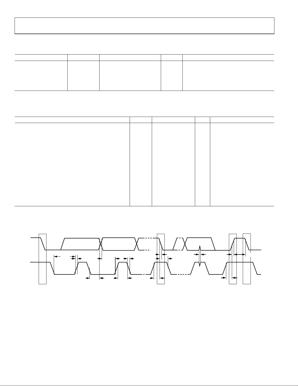
A master device must provide a hold time of at least 300 ns for the SDA signal to bridge the undefined region of the falling edge of SCL (see Figure 2).
Timing Diagram
400 kHz
SCL
0.6 µs
HIGH
1.3 µs
LOW
100 ns
SU, DAT
0 0.9 µs
HD, DAT
0.6 µs
SU, STA
HD, STA
1.3 µs
BUF
0.6 µs
SU, STO
300 ns
A
SCL
S Sr P S
S = START CONDITION
Sr = REPEATED START CONDITION
P = STOP CONDITION
t
LOW
t
HD, DAT
t
SU, DAT
t
t
HIGH
Figure 2. I
Rev. 0 | Page 6 of 44
F
t
2
C Timing Diagram
t
R
t
BU, STA
F
t
HD, STA
t
SP
t
BU, STO
t
R
t
BUF
10544-002
Data Sheet ADP5061
VIN1, VIN2, VIN3 to AGND
–0.5 V to +20 V
Stresses a bove those l isted under Absolute Maximum Ratings
may cause permanent damage to the device. This is a stress
rating only; functional operation of the device at these or any
other conditions above those indicated in the operational
section of this specification is not implied. Exposure to absolute
maximum rating conditions fo r extended periods may affect
device reliability.
ABSOLUTE MAXIMUM RATINGS
Table 4. Absolute Maximum Ratings
Parameter Rating
All Other Pins to AGND –0.3 V to +6 V
Continuous Drain Current, Battery Supple-
mentary Mode, from ISO_Bx to ISO_Sx
Storage Temperature Range –65°C to +150°C
Operating Junction Temperature Range –40°C to +125°C
Soldering Conditions JEDEC J-STD-020
2.1 A
THERMAL RESISTANCE
θJA is specified for the worst-case conditions, that is, θJA is
specified for a device soldered in a circuit board for surfacemount packages.
Table 5. Thermal Resistance
Package Type θJA θJC θJB Unit
20-Lead WLC SP1 46.8 0.7 9.2 °C/W
1
5 × 4 array, 0.5 mm pitch (2.6 mm × 2.0 mm); based on a JEDEC 2S2P, 4-layer
board with 0 m/sec airflow.
Maximum Power Dissipation
The maximum safe power dissipation in the ADP5061 package
is limited by the associated rise in junction temperature (T
the die. At a die temperature of approximately 150°C (the glass
transition temperature), the properties of the plastic change.
Even temporarily exceeding this temperature limit may change
the stresses that the package exerts on the die, thereby permanently shifting the parametric performance of the ADP5061.
Exceeding a junction temperature of 175°C for an extended
period can result in changes in the silicon devices, potentially
causing failure.
) on
J
ESD CAUTION
Rev. 0 | Page 7 of 44
ADP5061 Data Sheet
TOP VIEW
(BALL SI DE DOWN)
Not to Scale
1
A
B
C
D
E
2 3 4
BALL A1 CORNER
ILED
AGND
ISO_B3
ISO_B2
SDA
CBP
VIN3
VIN2
SCL
DIG_IO3
DIG_IO2
BAT_SNS
SYS_EN
THR
ISO_S3
ISO_S2
ISO_B1 VIN1 DIG_IO1ISO_S1
10544-003
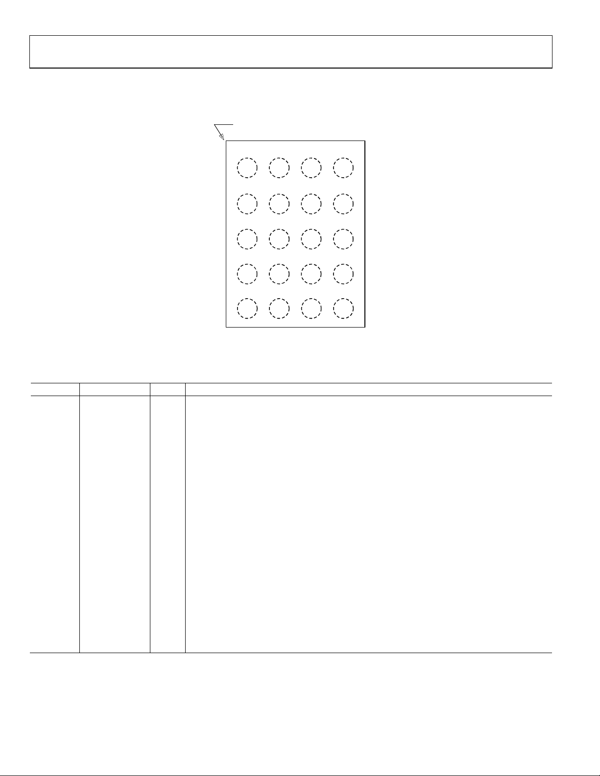
PIN CONFIGURATION AND FUNCTION DESCRIPTIONS
Figure 3. Pin Configuration
Table 6. Pin Function Descriptions
Pin No. Name Type1 Description
E2, D2, C2 ISO_S1, ISO_S2,
ISO_S3
I/O Linear Charger Supply Side Input to the Internal Isolation FET/Battery Current Regulation FET.
High current input/output.
E3, D3, C3 VIN1, VIN2, VIN3 I/O Power Connections to USB VBUS. These pins are high current inputs when in charging mode.
B1 AGND G Analog Ground.
E1, D1, C1 ISO_B1, ISO_B2,
I/O Battery Supply Side Input to Internal Isolation FET/Battery Current Regulation FET.
ISO_B3
A4 SCL I I2C-Compatible Interface Serial Clock.
A3 SDA I/O I2C-Compatible Interface Serial Data.
E4 DIG_IO1 GPIO Set Input Current Limit. This pin sets the input current limit directly. When DIG_IO1 = low or
high-Z, the input limit is 100 mA. When DIG_IO1 = high, the input limit is 500 mA.
2, 3
C4 DIG_IO2 GPIO Disable IC1. This pin sets the charger to the low current mode. When DIG_IO2 = low or high-Z, the
charger operates in normal mode. When DIG_IO2 = high, the LDO and the charger are disabled
and VINx current consumption is 280 µA (typical). 20 V VINx input protection is disabled and VINx
B4 DIG_IO3 GPIO Enable Charging. When DIG_IO3 = low or high-Z, charging is disabled. When DIG_IO3 = high,
B2 THR I Battery Pack Thermistor Connection. If this pin is not used, connect a dummy 10 kΩ resistor from THR
voltage level must be equal to or lower than 5.5 V.
charging is enabled.
2, 3
to GND.
2, 3
D4 BAT _ SNS I Battery Voltage Sense Pin.
A1 ILED O Open-Drain Output to Indicator LED.
A2 SYS_EN O System Enable. This is the battery OK flag/open-drain pull-down FET pin to enable the system
B3 CBP I/O Bypass Capacitor Input.
1
I is input, O is output, I/O is input/output, G is ground, and GPIO is factory programmable general-purpose input/output.
2
See the Digital Input and Output Options section for details.
3
DIG_IOx setting defines the initial state of the ADP5061. When the parameter or the mode that is related to each DIG_IOx pin setting is changed (by programming the
equivalent I
when the battery level reaches the V
2
C register bit or bits), the I2C register setting dominates over the DIG_IOx pin setting. VINx connection or disconnection resets control to the DIG_IOx pin.
Rev. 0 | Page 8 of 44
WEAK
level.
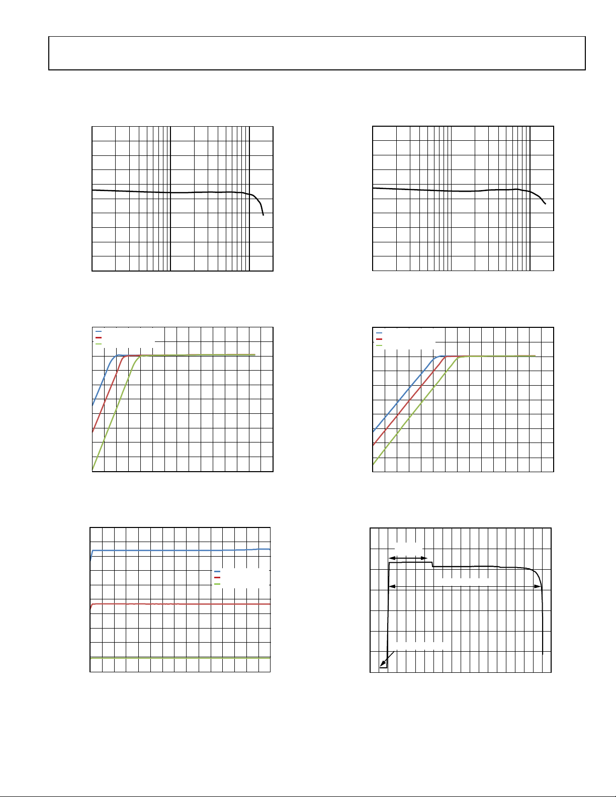
Data Sheet ADP5061
4.35
SYSTEM VOLTAGE (V)
4.5
4.0 4.4 4.8 5.2 5.6 6.0 6.4 6.8
SYSTEM VOLTAGE (V)
INPUT VOLTAGE (V)
LOAD = 100mA
LOAD = 500mA
LOAD = 1000mA
10544-005
0
100
200
300
400
500
600
700
800
900
1000
2.7 3.2 3.7 4.2
CHARGE CURRENT (mA)
BATTERY VOLTAGE (V)
LIMIT = 900mA
LIMIT = 500mA
LIMIT = 100mA
10544-006
4.95
4.96
4.97
4.98
4.99
5.00
5.01
5.02
5.03
5.04
5.05
0.01 0.1 1
SYSTEM VOLTAGE (V)
SYSTEM OUTPUT CURRENT ( A)
10544-007
5.4
4.0 4.4 4.8 5.2 5.6 6.0 6.4 6.8
SYSTEM VOLTAGE (V)
INPUT VOLTAGE (V)
LOAD = 100mA
LOAD = 500mA
LOAD = 1000mA
10544-008
0
100
200
300
400
500
600
700
2.3 2.8 3.3 3.8 4.3
CHARGE CURRENT (mA)
BATTERY VOLTAGE (V)
WEAK
CHARGE
FAST CHARGE
TRICKLE CHARGE
10544-009
TYPICAL PERFORMANCE CHARACTERISTICS
V
= 5.0 V, C
VIN
4.34
4.33
4.32
4.31
4.30
4.29
4.28
4.27
4.26
4.25
0.01 0.1 1
Figure 4. System Voltage vs. System Output Current, LDO Mode,
= 10 µF, C
VIN
SYSTEM OUTPUT CURRENT ( A)
= 44 µF, C
ISO_S
VSYSTEM[2:0] = 000 (Binary) = 4.3 V
= 22 µF, CBP = 10 nF, all registers at default values, unless otherwise noted.
ISO_B
10544-004
Figure 7. System Voltage vs. System Output Current, LDO Mode, V
VSYSTEM[2:0] = 111 (Binary) = 5.0 V
= 6.0 V,
VIN
4.4
4.3
4.2
4.1
4.0
3.9
3.8
3.7
3.6
3.5
Figure 5. Output Voltage vs. Input Voltage (In Dropout), LDO Mode,
VSYSTEM[2:0] = 000 (Binary) = 4.3 V
Figure 6. Input Current-Limited Charge Current vs. Battery Voltage
5.2
5.0
4.8
4.6
4.4
4.2
4.0
3.8
3.6
3.4
Figure 8. Output Voltage vs. Input Voltage (In Dropout), LDO Mode,
VSYSTEM[2:0] = 111 (Binary) = 5.0 V
Figure 9. Battery Charge Current vs. Battery Voltage, ICHG[4:0] = 01001
(Binary) = 500 mA, ILIM[3:0] = 1111 (Binary) = 2100 mA
Rev. 0 | Page 9 of 44
ADP5061 Data Sheet
20
22
24
26
28
30
32
34
36
38
40
2.7 3.2 3.7 4.2
ISOLATION FET RESISTANCE (mΩ)
BATTERY VOLTAGE (V)
10544-010
0
0.5
1.0
1.5
2.0
2.5
3.0
3.5
4.0
0 2 4 6 8
VINx CURRENT (mA)
INPUT VOLTAGE (V)
DEFAULT STARTUP
DIS_LDO = HIGH
DIS_IC1 = HIGH
10544-011
20
22
24
26
28
30
32
34
36
38
40
0 0.5 1.0 1.5 2.0
ISOLATION FET RESISTANCE (mΩ)
LOAD CURRENT ( A)
10544-012
0
0.1
0.2
0.3
0.4
0.5
0.6
0.7
3.0
3.2
3.4
3.6
3.8
4.0
4.2
4.4
0 50 100 150
CHARGE CURRENT (A)
BATTERY VOLTAGE (A)
CHARGE TIM E ( min)
V
BAT_SNS
I
ISO_B
10544-013
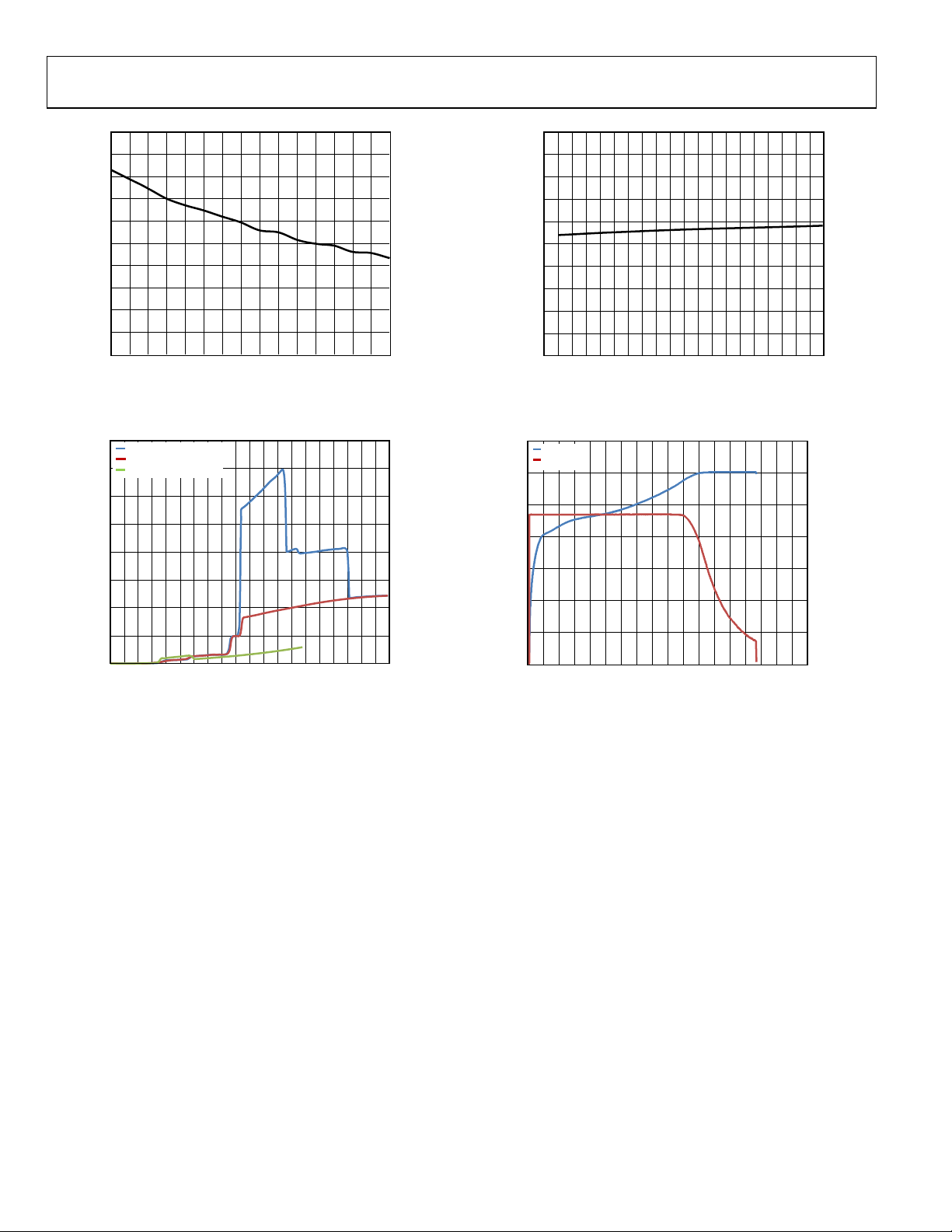
Figure 10. Ideal Diode RON vs. Battery Voltage, I
Figure 11. VINx Current vs. VINx Voltage
= 500 mA, VINx Open
ISO_S
Figure 12. Ideal Diode RON vs. Load Current, V
ISO_B
= 3.6 V
Figure 13. Charge Profile, ILIM[3:0] = 0110 (Binary) = 500 mA, Battery
Capacity = 925 mAh
Rev. 0 | Page 10 of 44
Data Sheet ADP5061
0
0.1
0.2
0.3
0.4
0.5
0.6
0.7
0.8
0.9
1.0
1.1
1.2
1.3
1.4
1.5
–40 –15 10 35 60 85
STANDBY CURRENT (µA)
AMBIENT TEMPERATURE (°C)
V
ISO_B
= 3.6V
V
ISO_B
= 4.2V
V
ISO_B
= 5.5V
10544-014
0
0.05
0.10
0.15
0.20
0.25
0.30
0.35
0.40
0.45
0.50
–40 –25 –10 5 20 35 50 65 80 95 110 125
VINx QUIE S CE NT CURRENT (mA)
AMBIENT TEMPERATURE (°C)
V
IN
= 4.0V
V
IN
= 5.0V
V
IN
= 5.5V
10544-015
–0.5
–0.4
–0.3
–0.2
–0.1
0
0.1
0.2
0.3
0.4
0.5
–40 –25 –10 5 20 35 50 65 80 95 110 125
SYSTEM VOLTAGE ACCURACY (%)
AMBIENT TEMPERATURE (°C)
V
ISO_S
= 4.3V
V
ISO_S
= 5.0V
10544-016
–0.5
–0.4
–0.3
–0.2
–0.1
0
0.1
0.2
0.3
0.4
0.5
–40 –25 –10 5 20 35 50 65 80 95 110 125
SYSTEM VOLTAGE ACCURACY (%)
AMBIENT TEMPERATURE (°C)
V
ISO_S
= 4.3V
V
ISO_S
= 5.0V
10544-017
0
0.5
1.0
1.5
2.0
2.5
3.0
3.5
4.0
4.5
5.0
–40 –25 –10 5 20 35 50 65 80 95 110 125
VINx QUIE S CE NT CURRENT (mA)
AMBIENT TEMPERATURE (°C)
VIN = 4.0V
V
IN
= 5.0V
VIN = 6.7V
10544-018
–0.5
–0.4
–0.3
–0.2
–0.1
0
0.1
0.2
0.3
0.4
0.5
–40 –25 –10 5 20 35 50 65 80 95 110 125
VTRM VOLTAGE ACCURACY (%)
AMBIENT TEMPERATURE (°C)
V
TRM
= 3.8V
V
TRM
= 4.2V
V
TRM
= 4.5V
10544-019
TEMPERATURE CHARACTERISTICS
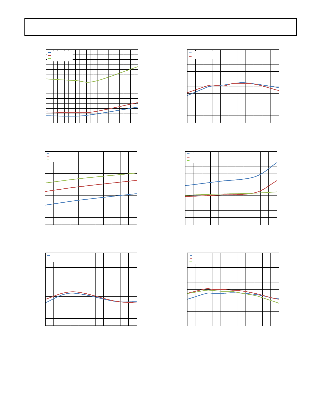
Figure 14. Battery Leakage Current vs. Ambient Temperature
Figure 15. VINx Quiescent Current vs. Ambient Temperature, DIS_IC1 = High
Figure 17. System Voltage vs. Temperature, Trickle Charge Mode,
V
= 4.3 V and VINx = 5.0 V, or V
ISO_S
= 5.0 V and VINx = 6.0 V
ISO_S
Figure 18. VINx Quiescent Current vs. Ambient Temperature, LDO Mode
Figure 16. LDO Mode Voltage vs. Ambient Temperature,
Load = 100 mA, V
= 5.5 V
VIN
Figure 19. Termination Voltage vs. Ambient Temperature
Rev. 0 | Page 11 of 44
ADP5061 Data Sheet
1.4
–40 –15 10 35
60 85 110
CHARGE CURRENT (A)
AMBIENT TEMPERATURE (°C)
I
CHG
= 750mA
I
CHG
= 500mA
I
CHG
= 1300mA
10544-020
AMBIENT TEMPERATURE (°C)
6.80
6.85
6.90
6.95
7.00
–40 –25 –10 5 20 35 50 65 80 95 110 125
VIN OVERVOLTAGE THRESHOL D ( V )
10544-021
1.6
–40 –25 –10 5 20 35 50 65 80 95 110 125
INPUT CURRENT LIMIT ( A)
AMBIENT TEMPERATURE (°C)
I
LIM
= 1500mA
I
LIM
= 900mA
I
LIM
= 500mA
I
LIM
= 100mA
10544-022
1.3
1.2
1.1
1.0
0.9
0.8
0.7
0.6
0.5
0.4
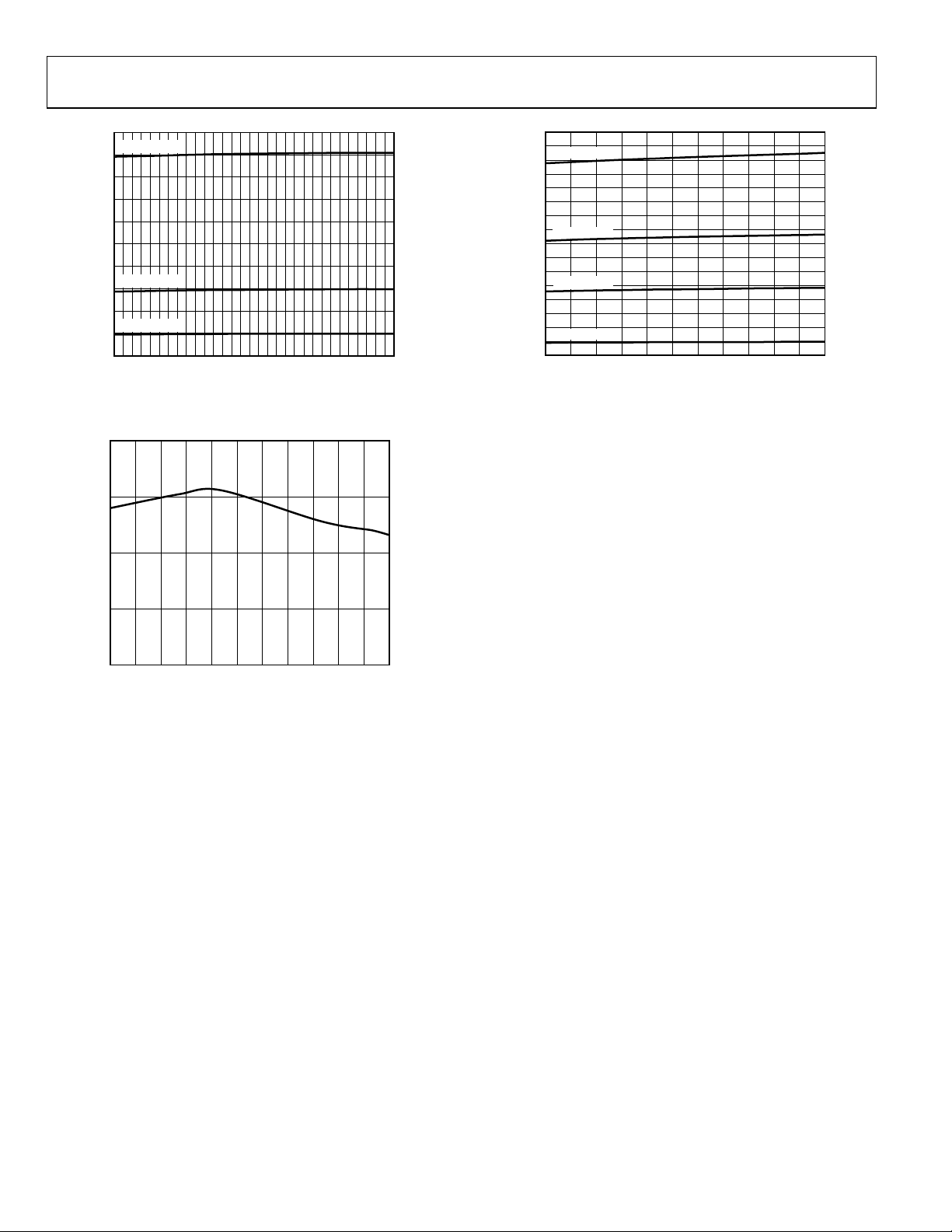
Figure 20. Fast Charge CC Mode Current vs. Ambient Temperature
1.5
1.4
1.3
1.2
1.1
1.0
0.9
0.8
0.7
0.6
0.5
0.4
0.3
0.2
0.1
0
Figure 22. Input Current Limit vs. Ambient Temperature
Figure 21. VINx Overvoltage Threshold vs. Ambient Temperature
Rev. 0 | Page 12 of 44
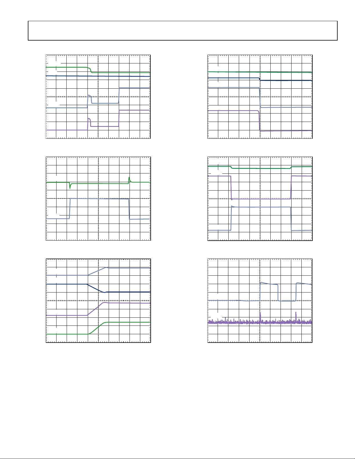
Data Sheet ADP5061
I
VIN
I
ISO_B
V
VIN
V
ISO_S
10544-023
I
ISO_S
V
ISO_S
10544-024
I
ISO_B
V
ISO_S
V
VIN
I
VIN
10544-025
I
VIN
I
ISO_B
V
VIN
V
ISO_S
10544-026
I
ISO_S
I
ISO_B
V
ISO_S
10544-027
I
ISO_B
V
ISO_B
10544-028
TYPICAL WAVEFORMS
Figure 23. Charging Startup, V
ICHG[4:0] = 01110 (Binary) = 750 mA
Figure 24. Load Transient, I
= 5.0 V, ILIM[3:0] = 0110 (Binary) = 500 mA,
VIN
Load = 300 mA to 1500 mA to 300 mA
ISO_Sx
Figure 26. VBUS Disconnect
Figure 27. Load Transient. I
Load = 300 mA to 1500 mA to 300 mA,
ISO_Sx
EN_CHG = High, ILIM[3:0] = 0110 (Binary) = 500 mA
Figure 25. Input Current-Limit Transition from 100 mA to 900 mA,
ISO_Sx Load = 66 Ω, Charging = 750 mA
Figure 28. Battery Detection Waveform, VSYSTEM[2:0] = 000 (Binary) = 4.3 V,
No Battery
Rev. 0 | Page 13 of 44

ADP5061 Data Sheet
High = all charging modes enabled (fast, weak, trickle).
Yes
CHG
CHG
THEORY OF OPERATION
SUMMARY OF OPERATION MODES
Table 7. Summary of the ADP5061 Operation Modes
LDO
Mode Name
VINx
Condition
Battery Condition
Trickle
Charge
FET
State
IC Off, Standby 0 V Any battery condition Off Off On/Off Battery voltage
IC Off, Suspend 5 V Any battery condition Off Off On Battery voltage Disable IC1
LDO Mode Off, Isolation
5 V Any battery condition Off Off On Battery voltage Disable LDO and
FET On
LDO Mode Off, Isolation
5 V Any battery condition Off Off Off 0 V Enable battery
FET Off (System Off)
LDO Mode, Charger Off 5 V Any battery condition Off LDO Off 5.0 V Enable battery
Trickle Charge Mode 5 V Battery < V
Weak Charge Mode 5 V V
TRK_DEA D
≤ battery < V
Fast Charge Mode 5 V Battery ≥ V
On LDO Off 5.0 V Enable battery
TRK_DEAD
On CHG CHG 3.8 V Enable battery
WEAK
Off CHG CHG 3.8 V (min) Enable battery
WEAK
Charge Mode, No Battery 5 V Open Off LDO Off 5.0 V Enable battery
Charge Mode, Battery
5 V Short On LDO Off 5.0 V Enable battery
(ISO_Bx) Short
1
See Table 8 for details.
Battery
Isolation
FET
System
Voltage
ISO_Sx
or 0 V
Additional
Conditions
1
Disable IC1
enable isolation FET
charging
charging
charging
charging
charging
charging
charging
Table 8. Operation Mode Controls
2
C
Pin Configuration DIG_IOx
Equivalent I
Address, Data Description
Enable Battery Charging DIG_IO3 0x07, D0 Low = all charging modes disabled (fast, weak, trickle).
Disable IC1 DIG_IO2 0x07, D6
Disable IC1
1
VINx
Supply
Connected
LDO_FET ISO_FET
Low No Off On
High No Off On
Yes Off On
Disable LDO and Enable Isolation FET 0x07, D3, D0 Low = LDO enabled.
High = LDO disabled. In addition, when EN_CHG = low, the
battery isolation FET is on; when EN_CHG = high, the battery
isolation FET is off.
1
When disable IC1 mode is active and the VINx supply is connected, the supply voltage level must fulfill the following condition: V
< VIN < 5.5 V.
ISO_B
Rev. 0 | Page 14 of 44
 Loading...