

ANALOG DEVICES ADP5040 Service Manual
Micro PMU with 1.2 A Buck Regulator
SW
C3
1µF
09665-001
FB2
R4
R2
R1
R3
FB3
R3
R7
C2
2.2µF
C4
2.2µF
VOUT2
VOUT1
FB1
V
IN1
= 2.3V TO
5.5V
VIN1
EN1
VIN2
EN2
EN3
VIN3
V
IN3
= 1.7V
TO 5.5V
EN_LDO2
LDO2
(ANALOG)
BUCK
PGND
MODE
VOUT3
LDO1
(DIGITAL)
EN_LDO1
AVIN
AVIN
R
FILT
= 30Ω
C5
4.7µF
V
IN2
= 1.7V
TO 5.5V
V
OUT1
AT
1.2A
V
OUT2
AT
300mA
V
OUT3
AT
300mA
C6
10µF
L1
1µH
C1
1µF
ON
OFF
ON
OFF
ON
OFF
AGND
EN_BK
PSM/PWM
FPWM
Data Sheet
FEATURES
Input voltage range: 2.3 V to 5.5 V
One 1.2 A buck regulator
Two 300 mA LDOs
20-lead, 4 mm × 4 mm LFCSP package
Overcurrent and thermal protection
Soft start
Undervoltage lockout
Buck key specifications
Output voltage range: 0.8 V to 3.8 V
Current mode topology for excellent transient response
3 MHz operating frequency
Peak efficiency up to 96%
Uses tiny multilayer inductors and capacitors
Mode pin selects forced PWM or auto PWM/PSM modes
100% duty cycle low dropout mode
LDOs key specifications
Output voltage range: 0.8 V to 5.2 V
Low V
from 1.7 V to 5.5 V
IN
Stable with 2.2 µF ceramic output capacitors
High PSRR
Low output noise
Low dropout voltage
−40°C to +125°C junction temperature range
and Two 300 mA LDOs
ADP5040
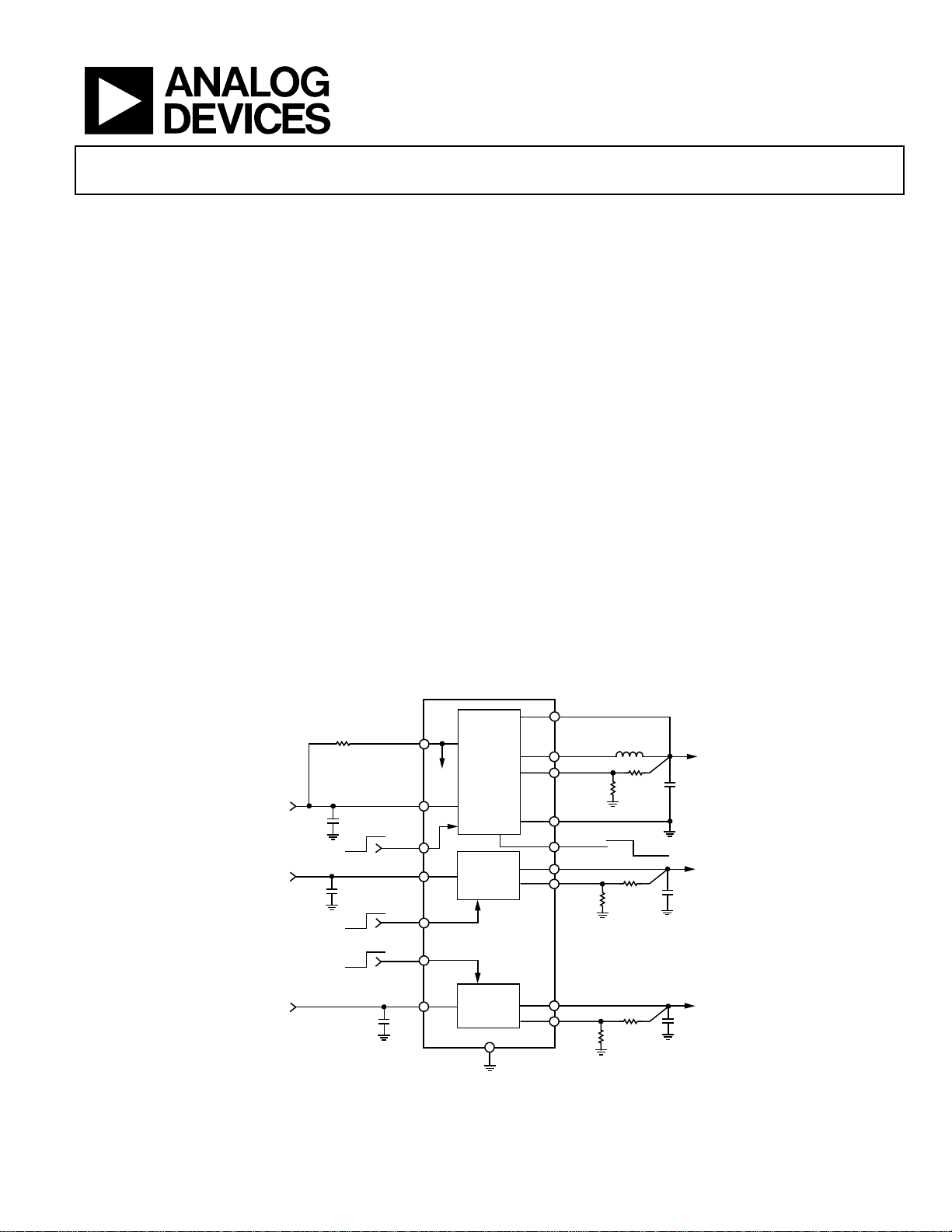
GENERAL DESCRIPTION
The ADP5040 combines one high performance buck regulator
and two low dropout regulators (LDO) in a small 20-lead
LFCSP to meet demanding performance and board space
requirements.
The high switching frequency of the buck regulator enables the use
of tiny multilayer external components and minimizes board space.
When the MODE pin is set to logic high, the buck regulator
operates in forced pulse width modulation (PWM) mode.
When the MODE pin is set to logic low, the buck regulator
operates in PWM mode when the load is around the nominal
value. When the load current falls below a predefined threshold
the regulator operates in power save mode (PSM) improving
the light-load efficiency. The low quiescent current, low
dropout voltage, and wide input voltage range of the ADP5040
LDOs extend the battery life of portable devices. The ADP5040
LDOs maintain a power supply rejection greater than 60 dB for
frequencies as high as 10 kHz while operating with a low headroom
voltage.
Each regulator in the ADP5040 is activated by a high level on
the respective enable pin. The output voltages of the regulators
are programmed though external resistor dividers to address a
variety of applications.
FUNCTIONAL BLOCK DIAGRAM
Rev. 0
Information furnished by Analog Devices is believed to be accurate and reliable. However, no
responsibility is assumed by Analog Devices for its use, nor for any infringements of patents or other
rights of third parties that may result from its use. Specifications subject to change without notice. No
license is granted by implication or otherwise under any patent or patent rights of Analog Devices.
Trademarks and registered trademarks are the property of their respec tive owners.
Figure 1.
One Technology Way, P.O. Box 9106, Norwood, MA 02062-9106, U.S.A.
Tel: 781.329.4700 www.analog.com
Fax: 781.461.3113 ©2011 Analog Devices, Inc. All rights reserved.

ADP5040 Data Sheet
TABLE OF CONTENTS
Features .............................................................................................. 1
General Description ......................................................................... 1
Functional Block Diagram .............................................................. 1
Revision History ............................................................................... 2
Specifications ..................................................................................... 3
General Specifications ................................................................. 3
Buck Specifications ....................................................................... 3
LDO1, LDO2 Specifications ....................................................... 4
Input and Output Capacitor, Recommended Specifications .. 5
Absolute Maximum Ratings ............................................................ 6
Thermal Resistance ...................................................................... 6
ESD Caution .................................................................................. 6
Pin Configuration and Function Descriptions ............................. 7
Theory of Operation ...................................................................... 25
REVISION HISTORY
12/11—Revision 0: Initial Version
Power Management Unit ........................................................... 25
Buck Section ................................................................................ 26
LDO Section ............................................................................... 27
Applications Information .............................................................. 29
Buck External Component Selection ....................................... 29
LDO External Component Selection ...................................... 30
Power Dissipation/Thermal Considerations ............................. 31
Application Diagram ................................................................. 33
PCB Layout Guidelines .................................................................. 34
Suggested Layout ........................................................................ 34
Bill of Materials ........................................................................... 35
Factory Programmable Options ................................................... 36
Outline Dimensions ....................................................................... 37
Ordering Guide .......................................................................... 37
Rev. 0 | Page 2 of 40

Data Sheet ADP5040
SPECIFICATIONS
GENERAL SPECIFICATIONS
AVIN, VIN1 = 2.3 V to 5.5 V; AVIN, VIN1 ≥VIN2, VIN3; VIN2, VIN3 = 1.7 V to 5.5 V, TJ = −40°C to +125°C for minimum/maximum
specifications, and T
Table 1.
Parameter Symbol Description Min Typ Max Unit
AVIN UNDERVOLTAGE LOCKOUT UVLO
Input Voltage Rising UVLO
Option 0 2.275 V
Option 1 3.9 V
Input Voltage Falling UVLO
Option 0 1.95 V
Option 1 3.1 V
SHUTDOWN CURRENT I
Thermal Shutdown Threshold TSSD TJ rising 150 °C
Thermal Shutdown Hysteresis TS
STA RT-UP TIME1
BUCK t
LDO1, LDO2 t
Enx, MODE, INPUTS
Input Logic High VIH 2.5 V ≤ AVIN ≤ 5.5 V 1.2 V
Input Logic Low VIL 2.5 V ≤ AVIN ≤ 5.5 V 0.4 V
Input Leakage Current V
1
Start-up time is defined as the time from the moment EN1 = EN2 = EN3 transfers from 0 V to V
nominal level. Start-up times are shorter for individual channels if another channel is already enabled. See the Typical Performance Characteristics section for more
information.
= 25°C for typical specifications, unless otherwise noted.
A
AVIN
AVINRISE
AVI NFAL L
ENx = GND 0.1 2 µA
GND-SD
20 °C
SD-HYS
250 µs
STA RT1
V
STA RT2
ENx = AVIN or GND 0.05 1 µA
I-LEAKAGE
OUT2
, V
= 3.3 V 85 µs
OUT3
to the moment VOUT1, VOUT2, and VOUT3 reache 90% of their
AVIN
BUCK SPECIFICATIONS
AVIN, VIN1 = 2.3 V to 5.5 V; V
specifications, and T
= 25°C for typical specifications, unless otherwise noted.1
A
Table 2.
Parameter Symbol Test Conditions/Comments Min Typ Max Unit
INPUT CHARACTERISTICS
Input Voltage Range
OUTPUT CHARACTERISTICS
Output Voltage Accuracy V
Line Regulation (ΔV
Load Regulation (ΔV
VOLTAGE FEEDBACK V
PWM TO POWER SAVE MODE
CURRENT THRESHOLD
INPUT CURRENT CHARACTERISTICS
DC Operating Current I
Shutdown Current I
= 1.8 V; L = 1 µH; CIN = 10 µF; C
OUT1
V
2.3 5.5 V
IN1
PWM mode,
OUT1
I
LOAD
)/ΔV
PWM mode −0.05 %/V
IN1
)/ΔI
I
OUT1
LOAD
MODE = ground
I
LOAD
FB1
I
PSM_L
NOLO AD
OUT1/VOUT1
OUT1/VOUT1
= 10 µF; TJ= −40°C to +125°C for minimum/maximum
OUT
−3 +3 %
= 0 mA to 1200 mA
= mA to 1200 mA, PWM mode −0.1 %/A
0.485 0.5 0.515 V
100 mA
= 0 mA, device not switching, all other
21 35 μA
channels disabled
EN1 = 0 V, TA = TJ = −40°C to +125°C 0.2 1.0 μA
SHTD
Rev. 0 | Page 3 of 40

ADP5040 Data Sheet
Parameter Symbol Test Conditions/Comments Min Typ Max Unit
SW CHARACTERISTICS
SW On Resistance R
PFET, AVIN = VIN1 = 5 V 140 190 mΩ
R
NFET, AVIN = VIN1 = 5 V 150 210 mΩ
Current Limit I
ACTIVE PULL-DOWN EN1 = 0 V 85 Ω
OSCILLATOR FREQUENCY F
1
All limits at temperature extremes are guaranteed via correlation using standard statistical quality control (SQC).
LDO1, LDO2 SPECIFICATIONS
V
, V
= (V
IN2
IN3
OUT2,VOUT3
T
= −40°C to +125°C for minimum/maximum specifications, and TA = 25°C for typical specifications, unless otherwise noted. 1
J
Table 3.
Parameter Symbol Conditions Min Typ Max Unit
INPUT VOLTAGE RANGE V
OPERATING SUPPLY CURRENT
Bias Current per LDO2 I
Total System Input Current IIN Includes all current into AVIN, VIN1, VIN2 and VIN3
LDO1 or LDO2 Only I
LDO1 and LDO2 Only I
OUTPUT VOLTAGE ACCURACY V
100 μA < I
REFERENCE VOLTAGE V
REGULATION
Line Regulation (ΔV
I
Load Regulation3 (ΔV
DROPOUT VOLTAGE4 V
V
V
V
V
ACTIVE PULL-DOWN R
CURRENT-LIMIT THRESHOLD5 I
OUTPUT NOISE OUT
10 Hz to 100 kHz, V
10 Hz to 100 kHz, V
OUT
10 Hz to 100 kHz, V
10 Hz to 100 kHz, V
+ 0.5 V) or 1.7 V (whichever is greater) to 5.5V; AVIN, VIN1 ≥ VIN2, VIN3; CIN = 1 μF , C
I
I
(ΔV
(ΔV
PFET
NFET, AVIN = VIN1 = 3.6 V 170 235 mΩ
NFET
LIMIT
2.5 3.0 3.5 MHz
OSC
, V
T
IN2
IN3
VIN2BIAS /IVIN3BIAS
OUT2, VOUT3
I
OUT3
OUT2
OUT2
OUT2
OUT2
V
V
, V
0.485 0.500 0.515 V
FB2
FB3
OUT2/VOUT2
OUT3/VOUT3
OUT2/VOUT2
OUT3/VOUT3
DROPOUT
PDLDO
T
LIMIT
)/ΔV
)/ΔV
)/ΔI
)/ΔI
EN2/EN3 = 0 V 600 Ω
10 Hz to 100 kHz, V
LDO2NOISE
10 Hz to 100 kHz, V
LDO1NOISE
IN2
IN3
OUT2
OUT3
V
V
OUT2
I
OUT2 = IOUT3
PFET, AVIN = VIN1 = 3.6 V 180 240 mΩ
PFET switch peak current limit 1600 1950 2300 mA
= 2.2 μF;
OUT
= −40°C to +125°C 1.7
J
= I
= 0 μA 10 30 μA
OUT4
60 100 μA
−3 +3 %
−0.03 +0.03 %/ V
IN2
IN3
IN2
IN3
= I
= 10 mA
OUT3
= I
= 300 mA
OUT3
= I
= 0 μA, all other channels disabled 53 μA
OUT3
= I
= 0 μA, buck disabled 74 μA
OUT3
< 300 mA, 100 μA < I
OUT2
= (V
+ 0.5 V) to 5.5 V,
OUT2
= (V
+ 0.5 V) to 5.5 V
OUT3
= (V
+ 0.5 V) to 5.5 V
OUT2
= (V
+ 0.5 V) to 5.5 V
OUT3
= I
= 1 mA
OUT3
< 300 mA
OUT3
165 245 μA
5.5 V
= 1 mA to 300 mA 0.002 0.0075 %/mA
= V
= V
= V
= V
= 5.0 V, I
OUT3
= 3.3 V, I
OUT3
= 2.5 V, I
OUT3
= 1.8 V, I
OUT3
OUT2
OUT2
OUT2
OUT2
= −40°C to +125°C 335 470 mA
J
OUT2
OUT2
OUT2
OUT2
= 5 V, V
IN3
= 5 V, V
IN3
= 5 V, V
IN3
= 5 V, V
IN2
= 5 V, V
IN2
= 5 V, V
IN2
= I
= 300 mA 72 mV
OUT3
= I
= 300 mA 86 140 mV
OUT3
= I
= 300 mA 107 mV
OUT3
= I
= 300 mA 180 mV
OUT3
= 3.3 V 123 μV rms
OUT3
= 2.8 V 110 μV rms
OUT3
= 1.5 V 59 μV rms
OUT3
= 3.3 V 140 μV rms
OUT2
= 2.8 V 129 μV rms
OUT2
= 1.5 V 66
OUT2
μV rms
Rev. 0 | Page 4 of 40

Data Sheet ADP5040
Parameter Symbol Conditions Min Typ Max Unit
POWER SUPPLY REJECTION
RATIO
100 kHz, V
1 MHz, V
1
All limits at temperature extremes are guaranteed via correlation using standard statistical quality control (SQC).
2
This is the input current into V
3
Based on an end-point calculation using 1 mA and 300 mA loads.
4
Dropout voltage is defined as the input-to-output voltage differential when the input voltage is set to the nominal output voltage. This applies only for output
voltages above 1.7 V.
5
Current-limit threshold is defined as the current at which the output voltage drops to 90% of the specified typical value. For example, the current limit for a 3.0 V
PSRR 1 kHz, V
and V
IN2
, which is not delivered to the output load.
IN3
= 100 mA
I
OUT
= 100 mA
I
OUT
= 100 mA
I
OUT
IN2, VIN3
IN2, VIN3
, V
IN2
= 3.3 V, V
= 3.3 V, V
= 3.3 V, V
IN3
, V
OUT2
OUT2, VOUT3
OUT2, VOUT3
= 2.8 V,
OUT3
= 2.8 V,
= 2.8 V,
output voltage is defined as the current that causes the output voltage to drop to 90% of 3.0 V, or 2.7 V.
INPUT AND OUTPUT CAPACITOR, RECOMMENDED SPECIFICATIONS
Table 4.
Parameter Symbol Conditions Min Typ Max Unit
INPUT CAPACITANCE (BUCK)1 C
OUTPUT CAPACITANCE (BUCK)2 C
INPUT AND OUTPUT CAPACITANCE3 (LDO1, LDO2) C
CAPACITOR ESR R
1
The minimum input capacitance should be greater than 4.7 µF over the full range of operating conditions. The full range of operating conditions in the application
must be considered during device selection to ensure that the minimum capacitance specification is met. X7R and X5R type capacitors are recommended, whereas
Y5V and Z5U capacitors are not recommended for use with the buck.
2
The minimum output capacitance should be greater than 7 µF over the full range of operating conditions. The full range of operating conditions in the application
must be considered during device selection to ensure that the minimum capacitance specification is met. X7R and X5R type capacitors are recommended, whereas
Y5V and Z5U capacitors are not recommended for use with the buck.
3
The minimum input and output capacitance should be greater than 0.70 µF over the full range of operating conditions. The full range of operating conditions in the
application must be considered during device selection to ensure that the minimum capacitance specification is met. X7R and X5R type capacitors are recommended,
whereas Y5V and Z5U capacitors are not recommended for use with LDOs.
TJ = −40°C to +125°C 4.7 40 µF
MIN1
TJ = −40°C to +125°C 7 40 µF
MIN2
TJ = −40°C to +125°C 0.70 µF
MIN34
TJ = −40°C to +125°C 0.001 1 Ω
ESR
66 dB
57 dB
60 dB
Rev. 0 | Page 5 of 40

ADP5040 Data Sheet
ABSOLUTE MAXIMUM RATINGS
Table 5.
Parameter Rating
AVIN to AGND −0.3 V to +6 V
VIN1 to AVIN −0.3 V to +0.3 V
PGND to AGDN −0.3 V to +0.3 V
VIN2, VIN3, VOUTx, ENx, MODE, FBx, SW to
AGND
SW to PGND −0.3 V to (VIN1 + 0.3 V)
Storage Temperature Range −65°C to +150°C
Operating Junction Temperature Range −40°C to +125°C
Soldering Conditions JEDEC J-STD-020
ESD Human Body Model 3000 V
ESD Charged Device Model 1500 V
ESD Machine Model 200 V
Stresses above those listed under Absolute Maximum Ratings
may cause permanent damage to the device. This is a stress
rating only; functional operation of the device at these or any
other conditions above those indicated in the operational
section of this specification is not implied. Exposure to absolute
maximum rating conditions for extended periods may affect
device reliability.
−0.3 V to (AVIN + 0.3 V)
THERMAL RESISTANCE
θJA is specified for the worst-case conditions, that is, a device
soldered in a circuit board for surface-mount packages.
Table 6. Thermal Resistance
Package Type θJA θJC Unit
20-Lead, 0.5 mm pitch LFCSP 38 4.2 °C/W
ESD CAUTION
Rev. 0 | Page 6 of 40
Data Sheet ADP5040
14
13
12
1
3
4
VOUT2
15 FB2
VIN2
FB1
11
VOUT1
FB3
VIN3
2
VOUT3
EN3
5
NC
7
VIN1
6
AVIN
8
SW
9
PGND
10
EN1
19
NC
20
NC
18
NC
17
MODE
16
EN2
ADP5040
TOP VIEW
(Not to S cale)
NOTES
1. EXPO S E D P AD M US T BE CONNECT E D TO
SYSTEM GROUND PLANE.
09665-002
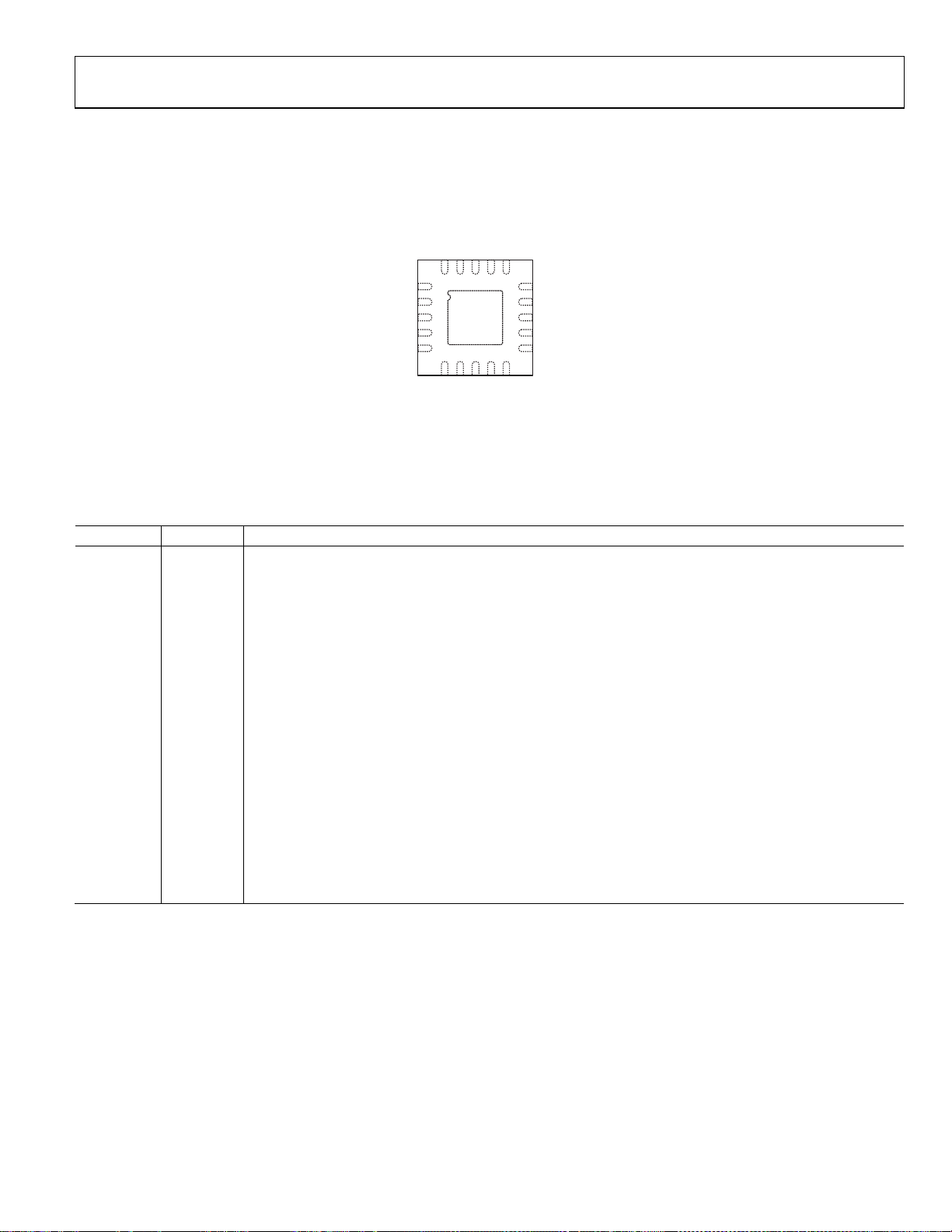
PIN CONFIGURATION AND FUNCTION DESCRIPTIONS
Figure 2. Pin Configuration—View from Top of the Die
Table 7. Preliminary Pin Function Descriptions
Pin No. Mnemonic Description
1 FB3 LDO2 Feedback Input.
2 VOUT3 LDO2 Output Voltage.
3 VIN3 LDO2 Input Supply (1.7 V to 5.5 V).
4 EN3 Enable LDO2. EN3 = high: turn on LDO2; EN3 = low: turn off LDO2.
6 AVIN Housekeeping Input Supply (2.3 V to 5.5 V).
7 VIN1 Buck Input Supply (2.3 V to 5.5 V).
8 SW Buck Switching Node.
9 PGND Dedicated Power Ground for Buck Regulator.
10 EN1 Enable Buck. EN1 = high: turn on buck; EN1 = low: turn off buck.
11 VOUT1 Buck Output Sensing Node.
12 FB1 Buck Feedback Input.
13 VIN2 LDO1 Input Supply (1.7 V to 5.5 V).
14 VOUT2 LDO1 Output Voltage.
15 FB2 LDO1 Feedback Input.
16 EN2 Enable LDO1. EN2 = high: turn on LDO1; EN2 = low: turn off LDO1.
17 MODE
5, 18, 19, 20 NC Not Connected.
0 EPAD Exposed Pad. ( AGND = Analog Ground). The exposed pad must be connected to the system ground plane.
Buck Mode. Mode = high: buck regulator operates in fixed PWM mode; mode = low: buck regulator operates in
power save mode (PSM) at light load and in constant PWM at higher load.
Rev. 0 | Page 7 of 40
ADP5040 Data Sheet
CH4 2.0V/DIV 1MΩ
B
W
500M
CH2 2.0V/DIV 1MΩ
B
W
20.0M
CH3 2.0V/DIV 1MΩ
B
W
500M
A CH2 1.88V 200µs/DIV
1.0MS/s
1.0µs/pt
4
2
3
V
OUT1
V
OUT2
V
OUT3
09665-003
CH1
CH2
CH3
CH4
A CH1 1.08V 200µs/DIV
5.0MS/s
200ns/pt
1
2
3
4
V
OUT3
V
OUT2
V
OUT1
I
IN
2.0V/DIV 1MΩ
B
W
20.0M
2.0V/DIV 1MΩ
B
W
20.0M
300mA/DIV 1MΩ
B
W
20.0M
2.0V/DIV 1MΩ
B
W
20.0M
09665-004
1.0
0
2.4 2.9 3.4 3.9 4.4 4.9 5.4
I
IN
(mA)
V
IN
(V)
0.1
0.2
0.3
0.4
0.5
0.6
0.7
0.8
0.9
09665-005
CH1
CH2
CH3
CH4
A CH1 2.32V 50µs/DIV
2.0MS/s
500ns/pt
1
2
3
4
SW
V
OUT1
EN
I
IN
4.0V/DIV 1MΩ
B
W
20.0M
3.0V/DIV 1MΩ
B
W
500M
200mA/DIV 1MΩ
B
W
20.0M
5.0V/DIV 1MΩ
B
W
500M
09665-006
CH1
CH2
CH3
CH4
A CH1 1.12V 50µs/DIV
2.0MS/s
500ns/pt
1
2
3
4
SW
V
OUT1
EN
I
IN
8.0V/DIV 1MΩ
B
W
20.0M
2.0V/DIV 1MΩ
B
W
500.0M
200mA/DIV 1MΩ
B
W
20.0M
5.0V/DIV 1MΩ
B
W
500.0M
09665-007
CH1
CH2
CH3
CH4
A CH1 640mV 50µs/DIV
2.0MS/s
500ns/pt
SW
V
OUT1
EN
I
IN
8.0V/DIV 1MΩ
B
W
20.0M
2.0V/DIV 1MΩ
B
W
500.0M
200mA/DIV 1MΩ
B
W
20.0M
5.0V/DIV 1MΩ
B
W
500.0M
1
2
3
4
09665-008
TYPICAL PERFORMANCE CHARACTERISTICS
VIN1 = VIN2 = VIN3 = AVIN = 5.0 V, TA = 25°C, unless otherwise noted.
Figure 3. 3-Channel Start-Up Waveforms
Figure 4. Total Inrush Current, All Channels Started Simultaneously
Figure 6. Buck Startup, V
Figure 7. Buck Startup, V
OUT1
OUT1
= 3.3 V, I
= 1.8 V, I
= 20 mA
OUT2
= 20 mA
OUT
Figure 5. System Quiescent Current (Sum of All the Input Currents) vs.
V
OUT1
= 1.8 V, V
Input Voltage
= V
OUT2
= 3.3 V, (UVLO = 3.3 V)
OUT3
Figure 8. Buck Startup, V
OUT1
= 1.2 V, I
= 20 mA
OUT
Rev. 0 | Page 8 of 40

Data Sheet ADP5040
3.90
3.70
0.01 0.1 1
OUTPUT VOLTAGE (V)
OUTPUT CURRE NT (A)
3.72
3.74
3.76
3.78
3.80
3.82
3.84
3.86
3.88
–40°C
+25°C
+85°C
09665-009
3.39
OUTPUT VOLTAGE (V)
1.820
1.815
1.810
1.800
1.805
1.795
1.790
1.780
1.785
0.01 0.1 1
OUTPUT VOLTAGE (V)
OUTPUT CURRE NT (A)
–40°C
+25°C
+85°C
09665-011
1.24
1.23
1.22
1.21
1.20
1.19
1.18
0.01 0.1 1
OUTPUT VOLTAGE (V)
OUTPUT CURRE NT (A)
–40°C
+25°C
+85°C
09665-012
3.90
3.88
3.86
3.70
3.72
3.74
3.76
3.78
3.80
3.82
3.84
0.01 0.1 1
OUTPUT VOLTAGE (V)
OUTPUT CURRE NT (A)
–40°C
+25°C
+85°C
09665-013
3.32
3.31
3.30
3.25
3.26
3.27
3.28
3.29
0.01 0.1 1
OUTPUT VOLTAGE (V)
OUTPUT CURRE NT (A)
–40°C
+25°C
+85°C
09665-014
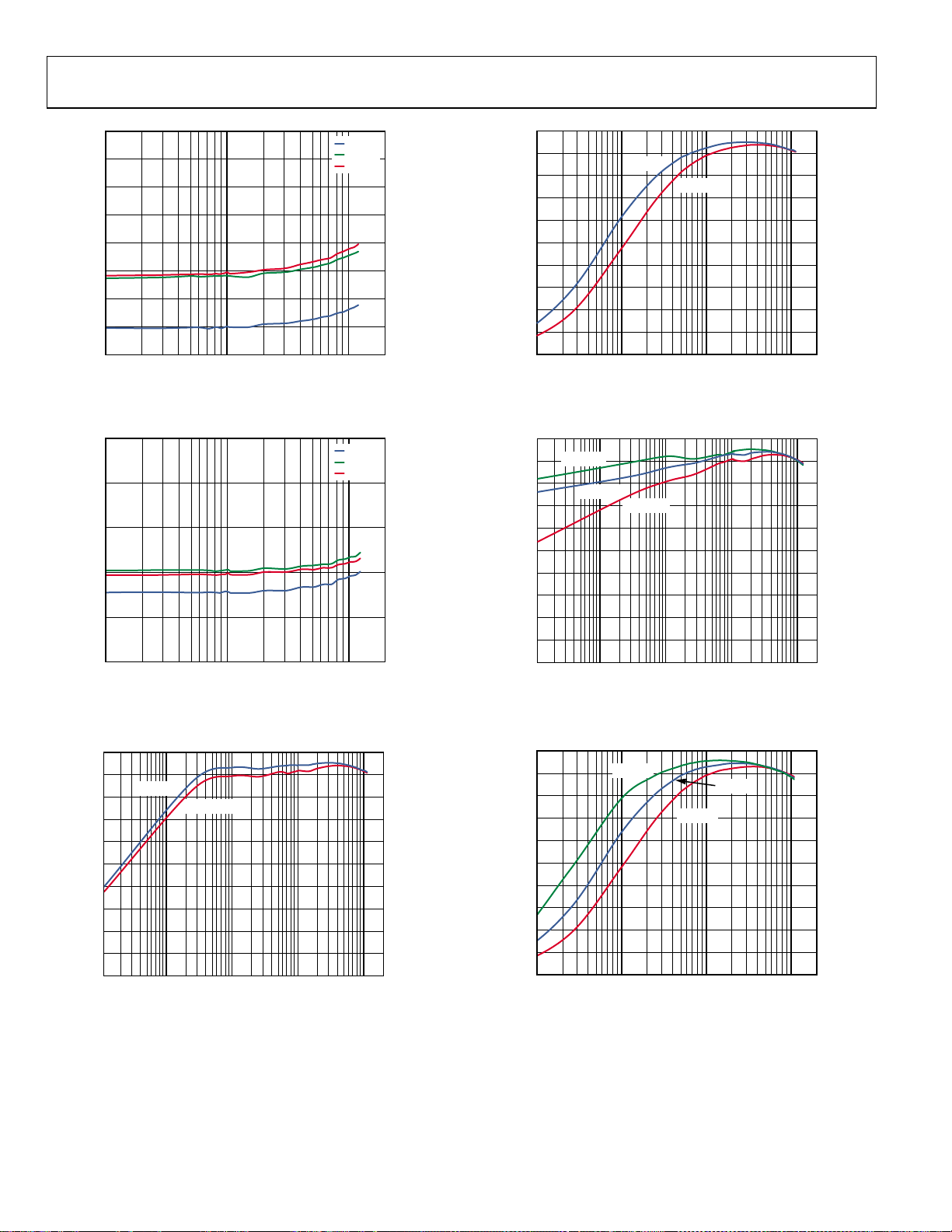
Figure 9. Buck Load Regulation Across Temperature, V
Auto Mode
3.37
3.35
3.33
3.31
3.29
3.27
3.25
0.01 0.1 1
OUTPUT CURRE NT (A)
Figure 10. Buck Load Regulation Across Temperature, V
Auto Mode
OUT1
OUT1
–40°C
+25°C
+85°C
= 3.8 V,
= 3.3 V,
Figure 12. Buck Load Regulation Across Temperature, V
OUT1
= 1.2 V,
Auto Mode
09665-010
Figure 13. Buck Load Regulation Across Temperature, V
OUT1
= 3.8 V,
PWM Mode
Figure 11. Buck Load Regulation Across Temperature, V
Auto Mode
OUT1
= 1.8 V,
Figure 14. Buck Load Regulation Across Temperature, V
OUT1
= 3.3 V,
PWM Mode
Rev. 0 | Page 9 of 40
ADP5040 Data Sheet
1.820
1.815
1.810
1.800
1.805
1.795
1.790
1.780
1.785
0.01 0.1 1
OUTPUT VOLTAGE (V)
OUTPUT CURRE NT (A)
–40°C
+25°C
+85°C
09665-015
1.205
1.200
1.195
1.185
1.190
1.180
0.01 0.1 1
OUTPUT VOLTAGE (V)
OUTPUT CURRE NT (A)
–40°C
+25°C
+85°C
09665-016
100
0
0.0001 0.001 0.01 0.1 1
EFFICIENCY (%)
OUTPUT CURRE NT (A)
10
20
30
40
50
60
70
80
90
V
IN
= 5.5V
V
IN
= 4.5V
09665-017
EFFICIENCY (%)
100
EFFICIENCY (%)
100
0
0.001 0.01 0.1 1
EFFICIENCY (%)
OUTPUT CURRE NT (A)
10
20
30
40
50
60
70
80
90
V
IN
= 5.5
VIN= 3.6
V
IN
= 4.5
09665-020
100
Figure 15. Buck Load Regulation Across Temperature,
= 1.8 V, PWM Mode
V
OUT1
Figure 16. Buck Load Regulation Across Temperature,
V
= 1.2 V, PWM Mode
OUT1
90
80
70
60
50
40
30
20
10
0
0.001 0.01 0.1 1
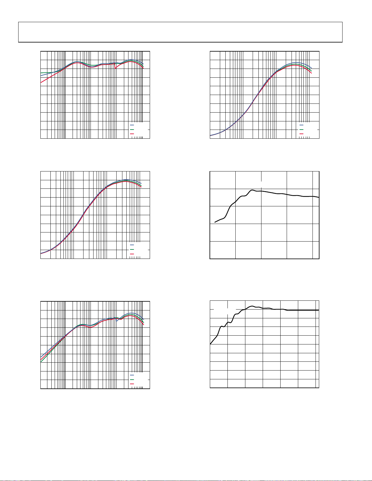
Figure 18. Buck Efficiency vs. Load Current, Across Input Voltage,
VIN= 3.6V
90
80
70
60
50
40
30
20
10
0
0.0001 0.001 0.01 0.1 1
Figure 19. Buck Efficiency vs. Load Current, Across Input Voltage,
V
VIN= 4.5V
V
VIN= 4.5V
VIN= 5.5V
OUTPUT CURRE NT (A)
= 3.8 V, PWM Mode
OUT1
VIN= 5.5V
OUTPUT CURRE NT (A)
= 3.3 V, Auto Mode
OUT1
09665-018
09665-019
Figure 17. Buck Efficiency vs. Load Current, Across Input Voltage,
V
= 3.8 V, Auto Mode
OUT1
Figure 20. Buck Efficiency vs. Load Current, Across Input Voltage,
= 3.3 V, PWM Mode
V
OUT1
Rev. 0 | Page 10 of 40

Data Sheet ADP5040
EFFICIENCY (%)
100
EFFICIENCY (%)
100
EFFICIENCY (%)
EFFICIENCY (%)
100
EFFICIENCY (%)
100
0
0.001 0.01 0.1 1
EFFICIENCY (%)
OUTPUT CURRE NT (A)
10
20
30
40
50
60
70
80
90
–40°C
+25°C
+85°C
09665-026
100
90
80
70
60
50
40
30
20
10
0
0.0001 0.001 0.01 0.1 1
VIN = 2.4V
V
= 3.6V
IN
= 4.5V
V
IN
V
= 5.5V
IN
OUTPUT CURRE NT (A)
Figure 21. Buck Efficiency vs. Load Current, Across Input Voltage,
V
= 1.8 V, Auto Mode
OUT1
09665-021
100
90
80
70
60
50
40
30
20
10
0
0.001 0.01 0.1 1
VIN = 2.4V
V
= 3.6V
IN
= 4.5V
V
IN
V
= 5.5V
IN
OUTPUT CURRE NT (A)
Figure 24. Buck Efficiency vs. Load Current, Across Input Voltage,
V
= 1.2 V, PWM Mode
OUT1
09665-024
90
80
70
60
50
40
30
20
10
0
0.001 0.01 0.1 1
OUTPUT CURRE NT (A)
Figure 22. Buck Efficiency vs. Load Current, Across Input Voltage,
= 1.8 V, PWM Mode
V
OUT1
90
80
70
60
50
40
30
20
10
0
0.0001 0.001 0.01 0.1 1
OUTPUT CURRE NT (A)
Figure 23. Buck Efficiency vs. Load Current, Across Input Voltage,
= 1.2 V, Auto Mode
V
OUT1
VIN = 2.4V
V
= 3.6V
IN
= 4.5V
V
IN
V
= 5.5V
IN
VIN = 2.4V
V
= 3.6V
IN
= 4.5V
V
IN
V
= 5.5V
IN
09665-022
09665-023
Rev. 0 | Page 11 of 40
90
80
70
60
50
40
30
20
10
0
0.0001 0.001 0.01 0.1 1
–40°C
+25°C
+85°C
OUTPUT CURRE NT (A)
Figure 25. Buck Efficiency vs. Load Current, Across Temperature,
= 5.0 V, V
V
IN
= 3.3 V, Auto Mode
OUT1
Figure 26. Buck Efficiency vs. Load Current, Across Temperature,
= 5.0 V, V
V
IN
= 3.3 V, PWM Mode
OUT1
09665-025
ADP5040 Data Sheet
EFFICIENCY (%)
100
EFFICIENCY (%)
100
0
0.0001 0.001 0.01 0.1 1
EFFICIENCY (%)
OUTPUT CURRE NT (A)
10
20
30
40
50
60
70
80
90
–40°C
+25°C
+85°C
09665-029
EFFICIENCY (%)
2.5
2.0
0.5
1.0
1.5
0
3.4 3.9 4.4 4.9 5.4
OUTPUT CURRE NT (A)
VIN (V)
V
OUT
= 3.3V
09665-031
2.0
1.8
0.2
0.4
0.6
0.8
1.6
1.4
1.2
1.0
0
2.4 3.93.42.9 4.4 4.9 5.4
OUTPUT CURRE NT (A)
VIN (V)
V
OUT
= 1.8V
09665-032
100
90
80
70
60
50
40
30
20
10
0
0.0001 0.001 0.01 0.1 1
OUTPUT CURRE NT (A)
–40°C
+25°C
+85°C
Figure 27. Buck Efficiency vs. Load Current, Across Temperature,
V
= 5.0 V, V
IN
90
80
70
60
50
40
30
20
10
0
0.001 0.01 0.1 1
= 1.8 V, Auto Mode
OUT1
OUTPUT CURRE NT (A)
–40°C
+25°C
+85°C
Figure 28. Buck Efficiency vs. Load Current, Across Temperature,
= 5.0 V, V
V
IN
= 1.8 V, PWM Mode
OUT1
09665-027
09665-028
100
90
80
70
60
50
40
30
20
10
0
0.001 0.01 0.1 1
OUTPUT CURRE NT (A)
–40°C
+25°C
+85°C
Figure 30. Buck Efficiency vs. Load Current, Across Temperature,
V
= 5.0 V, V
IN
= 1.2 V, PWM Mode
OUT1
Figure 31. Buck DC Current Capability vs. Input Voltage
09665-030
Figure 29. Buck Efficiency vs. Load Current, Across Temperature,
V
= 5.0 V, V
IN
= 1.2 V, Auto Mode
OUT1
Figure 32. Buck DC Current Capability vs. Input Voltage
Rev. 0 | Page 12 of 40
 Loading...