

Dual 3 MHz, 800 mA Buck
FEATURES
Main input voltage range: 2.3 V to 5.5 V
Two 800 mA buck regulators and two 300 mA LDOs
Tiny, 16-ball, 2 mm × 2 mm WLCSP package
Regulator accuracy: ±3%
Factory programmable VOUTx
3 MHz buck operation with forced PWM and auto PWM/PSM
modes
BUCK1/BUCK2: output voltage range from 0.8 V to 3.3 V
LDO1/LDO2: output voltage range from 0.8 V to 3.3V
LDO1/LDO2: low input supply voltage from 1.7 V to 5.5 V
LDO1/LDO2: high PSRR and low output noise
APPLICATIONS
Power for processors, ASICS, FPGAs, and RF chipsets
Portable instrumentation and medical devices
Space constrained devices
GENERAL DESCRIPTION
The ADP5033 combines two high performance buck regulators
and two low dropout regulators (LDO) in a tiny, 16-ball, 2 mm ×
2 mm WLCSP to meet demanding performance and board
space requirements.
Regulators with Two 300 mA LDOs
ADP5033
The high switching frequency of the buck regulators enables
tiny multilayer external components and minimizes the board
space. When the MODE pin is set high, the buck regulators
operate in forced PWM mode. When the MODE pin is set low,
the buck regulators operate in QPXFSTBWFNPEFP
UIFMPBEJT
CFMPXB
around the nominal value and the load current falls
predefined threshold, the regulator operates in 14.
improving the light load efficiency.
o bucks operate out of phase to reduce the input capacitor
The tw
requirement and noise.
The low quiescent current, low dropout voltage, and wide input
voltage range of the ADP5033 LDO extend the battery life of
portable devices. The ADP5033 LDOs maintain power supply
rejection greater than 60 dB for frequencies as high as 10 kHz
while operating with a low headroom voltage.
The regulators in the ADP5033 are activated by the ENA and
ENB pins. The specific channels controlled by ENA and ENB
are set by factory programming. A high voltage level applied to
the enable pins activates the regulators. The default output
voltages are factory programmable and can be set to a wide
range of options.
4M. When
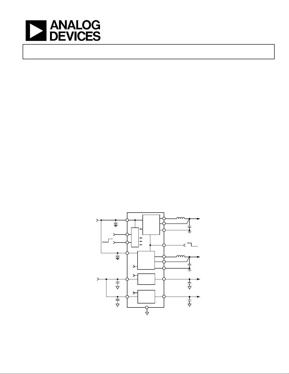
TYPICAL APPLICATION CIRCUIT
ADP5033
4.7µF
ON
4.7µF
C1
1µF
1µF
VIN1
ENA
ENB
VIN2
C2
VIN3
C3
VIN4
C4
UVLO
ACTIV. AND
EN2
EN3
EN4
2.3V TO 5.5V
OFF
1.7V TO 5. 5V
Rev. 0
Information furnished by Analog Devices is believed to be accurate and reliable. However, no
responsibility is assumed by Anal og Devices for its use, nor for any infringements of patents or ot her
rights of third parties that may result from its use. Specifications subject to change without notice. No
license is granted by implication or otherwise under any patent or patent rights of Analog Devices.
Trademarks and registered trademarks are the property of their respective owners.
BUCK1
EN1
MODE
EN2
EN3
EN4
MODE
BUCK2
LDO1
(ANALOG)
LDO2
(DIGITAL)
AGND
Figure 1.
L1 1µH
SW1
VOUT1
PGND1
MODE
SW2
VOUT2
PGND2
VOUT3
VOUT4
One Technology Way, P.O. Box 9106, Norwood, MA 02062-9106, U.S.A.
Tel: 781.329.4700 www.analog.com
Fax: 781.461.3113 ©2011 Analog Devices, Inc. All rights reserved.
PWM
L2 1µH
VOUT1 @
800mA
C5
10µF
PSM/PWM
VOUT2 @
800mA
C6
10µF
VOUT3 @
300mA
C7
1µF
VOUT4 @
300mA
C8
1µF
09788-001

ADP5033
TABLE OF CONTENTS
Features.............................................................................................. 1
Applications....................................................................................... 1
General Description ......................................................................... 1
Typical Application Circuit ............................................................. 1
Revision History ............................................................................... 2
Specifications..................................................................................... 3
General Specifications ................................................................. 3
BUCK1 and BUCK2 Specifications ........................................... 4
LDO1 and LDO2 Specifications................................................. 4
Input and Output Capacitor, Recommended Specifications.. 5
Absolute Maximum Ratings............................................................ 6
Thermal Resistance ...................................................................... 6
ESD Caution.................................................................................. 6
Pin Configuration and Function Descriptions............................. 7
Typical Performance Characteristics ............................................. 8
REVISION HISTORY
5/11—Revision 0: Initial Version
Power Dissipation and Thermal Considerations....................... 15
Buck Regulator Power Dissipation .......................................... 15
Junction Temperature................................................................ 16
Theory of Operation ...................................................................... 17
Power Management Unit........................................................... 17
BUCK1 and BUCK2 .................................................................. 18
LDO1 and LDO2........................................................................ 19
Applications Information.............................................................. 20
Buck External Component Selection....................................... 20
LDO Capacitor Selection .......................................................... 22
PCB Layout Guidelines.................................................................. 23
Typical Application Schematic ..................................................... 24
Outline Dimensions....................................................................... 25
Ordering Guide .......................................................................... 25
Rev. 0 | Page 2 of 28

ADP5033
SPECIFICATIONS
GENERAL SPECIFICATIONS
V
= V
= V
= V
IN1
IN2
IN3
T
= 25°C for typical specifications, unless otherwise noted.
A
= 2.3 V to 5.5 V; V
IN4
Table 1.
Parameter Symbol Test Conditions/Comments Min Typ Max Unit
INPUT VOLTAGE RANGE V
THERMAL SHUTDOWN
Threshold TSSD T
Hysteresis TS
START-UP TIME1
BUCK1, LDO1, LDO2 t
BUCK2 t
ENA, ENB, MODE INPUTS
Input Logic High VIH 1.1 V
Input Logic Low VIL 0.4 V
Input Leakage Current V
STANDBY CURRENT
All Channels Enabled I
All Channels Disabled I
VIN1 UNDERVOLTAGE LOCKOUT
High UVLO Input Voltage Rising UVLO
High UVLO Input Voltage Falling UVLO
Low UVLO Input Voltage Rising UVLO
Low UVLO Input Voltage Falling UVLO
1
Start-up time is defined as the time from V
IN1
START1
START2
STBY-NOSW
SHUTDOWN
> UVLO
= V
IN3
IN1
SD-HYS
= 1.7 V to 5.5 V; TJ = −40°C to +125°C for minimum/maximum specifications, and
IN4
, V
2.3 5.5 V
IN2
rising 150 °C
J
20 °C
250 μs
300 μs
0.05 1 μA
I-LEAKAGE
No load, no buck switching 108 175 μA
T
VIN1RISE
VIN1FALL
VIN1RISE
VIN1FALL
to VOUT1, VOUT2, VOUT3, and VOUT4 reaching 90% of their nominal levels.
VIN1RISE
= −40°C to +85°C 0.3 1 μA
J
3.9 V
3.1 V
2.275 V
1.95 V
Rev. 0 | Page 3 of 28

ADP5033
BUCK1 AND BUCK2 SPECIFICATIONS
V
= V
IN1
otherwise noted.
Table 2.
Parameter
INPUT CHARACTERISTICS
Input Voltage Range V
OUTPUT CHARACTERISTICS
Output Voltage Accuracy V
Line Regulation
Load Regulation
PSM CURRENT THRESHOLD
PSM to PWM Operation I
OPERATING SUPPLY CURRENT MODE = ground
BUCK1 Only I
BUCK2 Only IIN I
BUCK1 and BUCK2 IIN I
SW CHARACTERISTICS
SW On Resistance R
R
Current Limit I
ACTIVE PULL-DOWN R
OSCILLATOR FREQUENCY fSW 2.5 3.0 3.5 MHz
1
All limits at temperature extremes are guaranteed via correlation using standard statistical quality control (SQC).
= 2.3 V to 5.5 V; TJ = −40°C to +125°C for minimum/maximum specications, and TA = 25°C for typical specifications, unless
IN2
1
Symbol
, V
IN1
, V
OUT1
, V
V
OUT1
, I
I
OUT1
100 mA
PSM
IN
pFET at VIN1 = 5 V 145 235 mΩ
PFET
R
pFET at VIN1 = 3.6 V 180 295 mΩ
PFET
R
nFET at VIN1 = 5 V 110 190 mΩ
NFET
nFET at VIN1 = 3.6 V 125 220 mΩ
NFET
, I
LIMIT1
PDWN-B
Test Conditions/Comments Min Typ Max Unit
PWM mode, I
IN2
PWM mode; V
OUT2
PWM mode
OUT2
I
OUT2
LIMIT2
= 0 mA to 800mA, PWM mode
LOAD
I
= 0 mA, device not switching, all other channels disabled. 44 A
LOAD1
= 0 mA, device not switching, all other channels disabled. 55 A
LOAD2
= I
LOAD1
LOAD2
pFET switch peak current limit 1100 1350 mA
Channel disabled
= I
LOAD 1
IN1
= V
= 0 mA to 800 mA
LOAD 2
= 2.3 V to 5.5 V; I
IN2
LOAD1 = ILOAD2
= 0 mA to 800 mA −3 +3 %
= 0 mA, device not switching, LDO channels disabled. 67 A
2.3 5.5 V
−0.05
−0.1
75 Ω
%/V
%/A
LDO1 AND LDO2 SPECIFICATIONS
V
= (V
IN3
1 μF; T
Table 3.
Parameter Symbol Test Conditions/Comments Min Typ Max Unit
INPUT VOLTAGE RANGE V
OPERATING SUPPLY CURRENT
Bias Current per LDO2 I
I
I
Total System Input Current IIN Includes all current into VIN1, VIN2, VIN3, and VIN4
LDO1 or LDO2 Only I
LDO1 and LDO2 Only I
OUTPUT CHARACTERISTICS
Output Voltage Accuracy V
Line Regulation
Load Regulation3
DROPOUT VOLTAGE4 V
V
V
CURRENT-LIMIT THRESHOLD5 I
ACTIVE PULL-DOWN R
+ 0.5 V) or 1.7 V (whichever is greater) to 5.5 V, V
OUT3
= −40°C to +125°C for minimum/maximum specications, and TA = 25°C for typical specifications, unless otherwise noted.1
J
, V
1.7 5.5 V
IN3
IN4
I
VIN3BIAS/IVIN4BIAS
, V
OUT3
V
V
V
V
DROPOUT
LIMIT3
PDWN-L
OUT4
/V
/V
/I
/I
IN3
IN4
OUT3
OUT4
,
,
OUT3
OUT4
OUT3
OUT4
V
, I
335 600 mA
LIMIT4
Channel disabled 600 Ω
= I
OUT3
OUT4
= I
OUT3
OUT4
= I
OUT3
OUT4
= I
OUT3
OUT4
= I
OUT3
OUT4
100 µA < I
V
= (V
IN3
V
= (V
IN3
5.5 V, I
OUT3
= I
I
OUT3
OUT4
= V
OUT3
= V
OUT3
= V
OUT3
OUT3
OUT3
OUT3
= I
OUT4
OUT4
OUT4
IN4
= (V
+ 0.5 V) or 1.7 V (whichever is greater) to 5.5 V; CIN = C
OUT4
= 0 µA 10 30 µA
= 10 mA 60 100 µA
= 300 mA 165 245 µA
= 0 µA, all other channels disabled 53 µA
= 0 µA, buck channels disabled 74 µA
< 300 mA, 100 µA < I
+ 0.5 V) to 5.5 V, V
+ 0.5 V) to 5.5 V, V
= 1 mA
OUT4
IN4
= (V
= (V
IN4
OUT4
OUT4
< 300 mA;
+ 0.5 V) to 5.5 V
+ 0.5 V) to
OUT4
−3 +3 %
−0.03 +0.03 %/V
= 1 mA to 300 mA 0.001 0.003 %/mA
= 3.3 V 65 110 mV
= 2.5 V 85 mV
= 1.8 V 165 mV
OUT
=
Rev. 0 | Page 4 of 28
ADP5033
Parameter Symbol Test Conditions/Comments Min Typ Max Unit
POWER SUPPLY REJECTION
RATIO
Regulator LDO1 10 kHz, V
100 kHz, V
1 MHz, V
Regulator LDO2 10 kHz, V
100 kHz, V
1 MHz, V
1
All limits at temperature extremes are guaranteed via correlation using standard statistical quality control (SQC).2
2
This is the input current into VIN3/VIN4, which is not delivered to the output load.
3
Based on an endpoint calculation using 1 mA and 100 mA loads.
4
Dropout voltage is defined as the input-to-output voltage differential when the input voltage is set to the nominal output voltage. This applies only to output voltages
above 1.7 V.
5
Current-limit threshold is defined as the current at which the output voltage drops to 90% of the specified typical value. For example, the current limit for a 3.0 V
output voltage is defined as the current that causes the output voltage to drop to 90% of 3.0 V, or 2.7 V.
INPUT AND OUTPUT CAPACITOR, RECOMMENDED SPECIFICATIONS
TA = −40°C to +125°C, unless otherwise specified.
Table 4.
Parameter Symbol Min Typ Max Unit
SUGGESTED INPUT AND OUTPUT CAPACITANCE
BUCK1, BUCK2 Input Capacitor C
BUCK1, BUCK2 Output Capacitor C
LDO1, LDO21 Input and Output Capacitors C
CAPACITOR ESR R
1
The minimum input and output capacitance should be greater than 0.70 μF over the full range of operating conditions. The full range of operating conditions in the
application must be considered during device selection to ensure that the minimum capacitance specification is met. X7R- and X5R-type capacitors are
recommended; Y5V and Z5U capacitors are not recommended for use with LDOs.
PSRR
= 3.3 V, V
IN3
= 3.3 V, V
IN3
= 3.3 V, V
IN3
= 1.8 V, V
IN4
= 1.8 V, V
IN4
= 1.8 V, V
IN4
OUT3
OUT3
OUT3
OUT4
OUT4
OUT4
= 2.8 V, I
= 2.8 V, I
= 2.8 V, I
= 1.2 V, I
= 1.2 V, I
= 1.2 V, I
= 1 mA 60 dB
OUT3
= 1 mA 62 dB
OUT3
= 1 mA 63 dB
OUT3
= 1 mA 54 dB
OUT4
= 1 mA 57 dB
OUT4
= 1 mA 64 dB
OUT4
, C
MIN1
MIN1
MIN3
ESR
4.7 40 μF
MIN2
, C
10 40 μF
MIN2
, C
0.70 μF
MIN4
0.001 1 Ω
Rev. 0 | Page 5 of 28
ADP5033
ABSOLUTE MAXIMUM RATINGS
Table 5.
Parameter Rating
VIN1, VIN2, VIN3, VIN4, VOUT1, VOUT2,
VOUT3, VOUT4, ENA, MODE, ENB to
Ground
Storage Temperature Range –65°C to +150°C
Operating Junction Temperature Range –40°C to +125°C
Soldering Conditions JEDEC J-STD-020
ESD Human Body Model ±1500 V
ESD Charged Device Model ±500 V
ESD Machine Model ±100 V
Stresses above those listed under Absolute Maximum Ratings
may cause permanent damage to the device. This is a stress
rating only; functional operation of the device at these or any
other conditions above those indicated in the operational
section of this specification is not implied. Exposure to absolute
maximum rating conditions for extended periods may affect
device reliability.
For detailed information on power dissipation, see the Power
Dissipation and Thermal Considerations section.
–0.3 V to +6 V
THERMAL RESISTANCE
θJA and ΨJB are specified for the worst-case conditions, that is, a
device soldered in a circuit board for surface-mount packages.
Table 6. Thermal Resistance
Package Type θJA ΨJB Unit
16-Ball, 0.5 mm Pitch WLCSP 57 14 °C/W
ESD CAUTION
Rev. 0 | Page 6 of 28
ADP5033
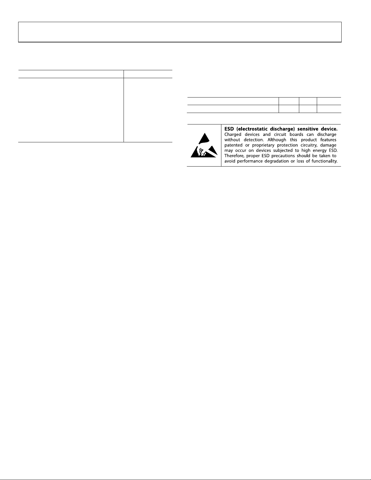
PIN CONFIGURATION AND FUNCTION DESCRIPTIONS
BALL A1
INDICATOR
VOUT3
A
AGND
B
C
PGND1
D
Figure 2. Pin Configuration—View from the Top of the Die
Table 7. Pin Function Descriptions
Pin No. Mnemonic Description
A1 VOUT3 LDO1 Output Voltage and Sensing Input.
A2 VIN3 LDO1 Input Supply (1.7 V to 5.5 V, VIN4 ≤ VIN1 = VIN2).
A3 VIN4 LDO2 Input Supply (1.7 V to 5.5 V, VIN3 ≤ VIN1 = VIN2).
A3 VOUT4 LDO2 Output Voltage and Sensing Input.
B1 AGND Analog Ground.
B2 MODE BUCK1/BUCK2 Operating Mode. MODE = high: forced PWM operation. MODE = low: auto PWM/PSM operation.
B3 ENA Regulator Enable Pin A, Active High. The regulators turned on with ENA are factory programmed.
B4 ENB Regulator Enable Pin B, Active High. The regulators turned on with ENB are factory programmed.
C1 VIN1 BUCK1 Input Supply (2.3 V to 5.5 V) and UVLO Detection. Connect VIN1 to VIN2.
C2 VOUT1 BUCK1 Output Voltage Sensing Input.
C3 VOUT2 BUCK2 Output Voltage Sensing Input.
C4 VIN2 BUCK2 Input Supply (2.3 V to 5.5 V). Connect VIN2 to VIN1.
D1 PGND1 Dedicated Power Ground for BUCK1.
D2 SW1 BUCK1 Switching Node.
D3 SW2 BUCK2 Switching Node.
D4 PGND2 Dedicated Power Ground for BUCK2.
234
1
VIN3
MODE
VIN1
VOUT1
SW1
TOP VIEW
(BALL SIDE DOWN)
Not to Scale
VIN4
ENA
VOUT2
SW2
VOUT4
ENB
VIN2
PGND2
09788-002
Rev. 0 | Page 7 of 28
ADP5033
TYPICAL PERFORMANCE CHARACTERISTICS
V
= V
= V
= V
IN1
IN2
IN3
= 5.0 V, TA = 25°C, unless otherwise noted.
IN4
140
120
100
80
60
40
QUIESCENT CURRENT (µA)
20
0
2.3 2.8 3.3 3.8 4.3 4.8 5.3
INPUT VOLTAGE (V)
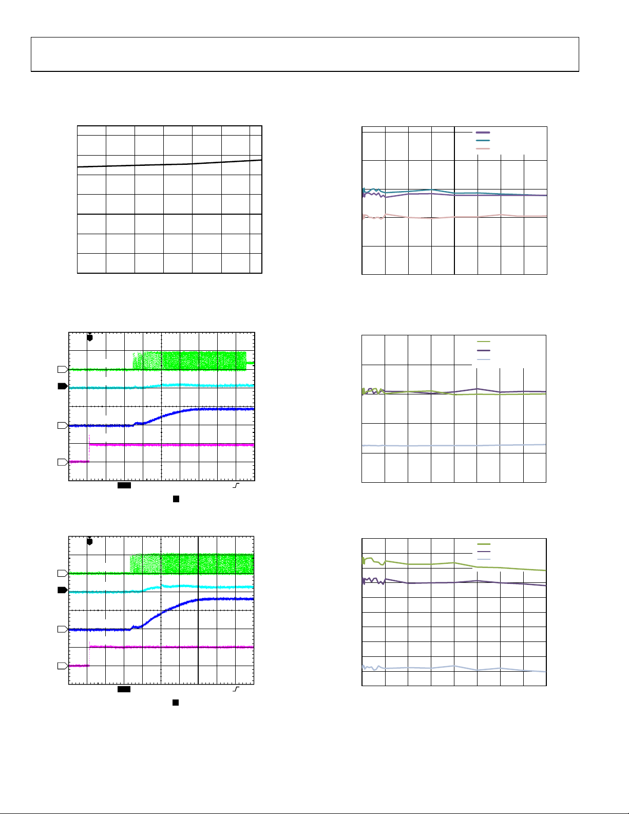
Figure 3. System Quiescent Current vs. Input Voltage, V
V
OUT2
4
2
1
3
= 1.8 V, V
= 1.2 V, V
OUT3
T
SW
VOUT
EN
I
IN
= 3.3 V, All Channels Unloaded
OUT4
OUT1
= 3.3 V,
3.35
3.33
3.31
A (V)
OUT
V
3.29
3.27
3.25
0 0.1 0.2 0.3 0.4 0.5 0.6 0.7 0.8
09788-139
I
OUT
(A)
Figure 6. BUCK1 Load Regulation Across Temperature, V
VIN = 4.2V, +85°C
VIN = 4.2V, +25°C
VIN = 4.2V, –40°C
= 3.3 V,
OUT1
09788-058
Auto Mode
A (V)
V
OUT
1.864
1.844
1.824
1.804
1.784
VIN = 3.6V, + 85°C
VIN = 3.6V, + 25°C
VIN = 3.6V, –40° C
CH1 2.00V
CH3 5.00V
Figure 4. Buck1 Startup, V
T
4
2
1
3
CH1 2.00V
CH3 5.00V
SW
VOUT
EN
I
IN
Figure 5. BUCK2 Startup, V
CH2 50.0mA Ω
CH4 5.00V
CH2 50.0mA Ω
CH4 5.00V
M 40.0µs A CH3 2. 2V
T 11.20%
OUT1
= 3.3 V, I
OUT1
= 10 mA
M 40.0µs A CH3 2.2V
T 11.20%
OUT2
= 1.8 V, I
OUT2
= 5 mA
09788-021
09788-020
Rev. 0 | Page 8 of 28
1.764
0 0.10.20.30.40.50.60.7 0.8
I
OUT
(A)
Figure 7. BUCK2 Load Regulation Across Temperature, V
Auto Mode
0.799
0.798
0.797
0.796
0.795
A (V)
0.794
OUT
V
0.793
0.792
0.791
0.790
0.789
0 0.1 0.2 0.3 0.4 0.5 0.6 0.7 0.8
I
OUT
(A)
VIN = 3.6V, + 85°C
VIN = 3.6V, + 25°C
VIN = 3.6V, –40° C
Figure 8. BUCK1 Load Regulation Across Input Voltage, V
PWM Mode
OUT2
OUT1
= 1.8 V,
= 3.3 V,
09788-057
09788-054
ADP5033
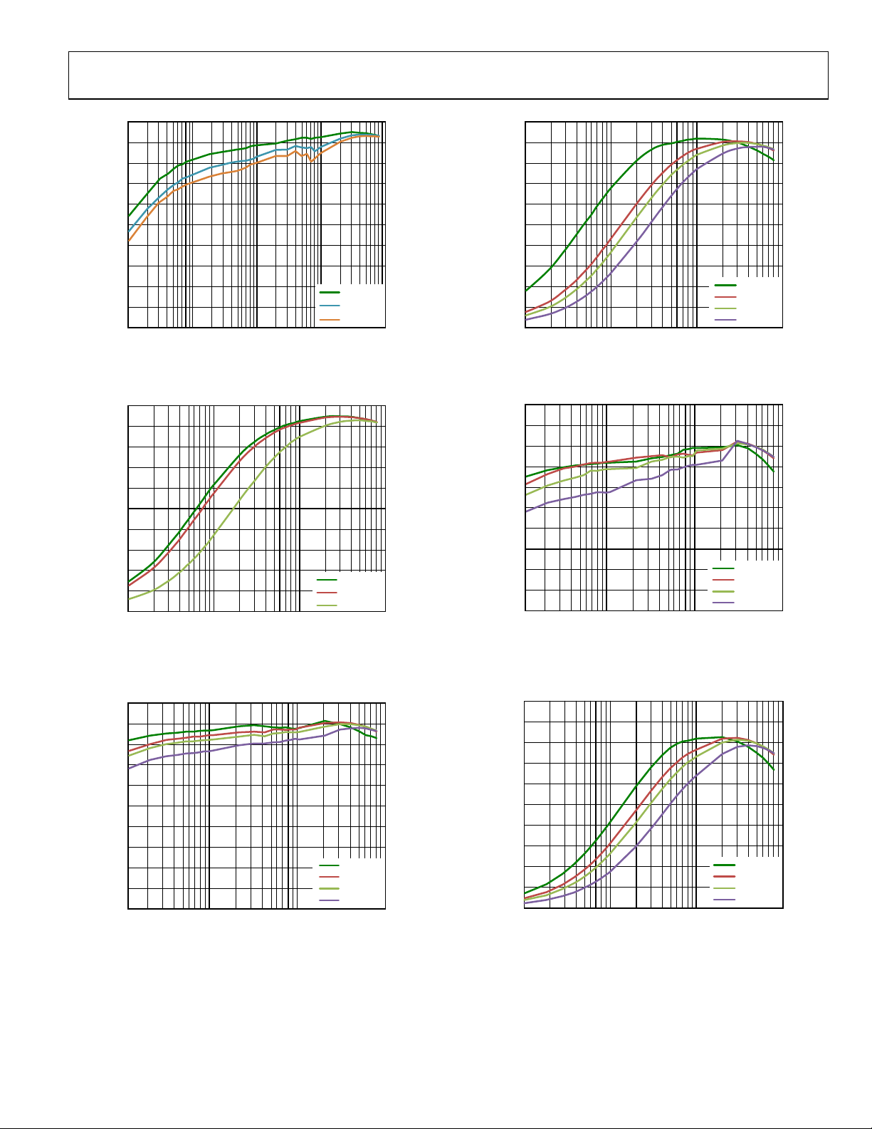
100
90
80
70
60
50
40
EFFICI ENCY (%)
30
20
10
0
0.0001 0.001 0.01 0.1 1
I
OUT
(A)
VIN = 3.9V
VIN = 4.2V
VIN = 5.5V
Figure 9. BUCK1 Efficiency vs. Load Current, Across Input Voltage,
= 3.3 V, Auto Mode
V
OUT1
100
90
80
70
60
50
40
EFFICI ENCY (%)
30
20
10
0
0.001 0.01 0.1 1
I
OUT
(A)
VIN = 3.9V
VIN = 4.2V
VIN = 5.5V
Figure 10. BUCK1 Efficiency vs. Load Current, Across Input Voltage,
= 3.3 V, PWM Mode
V
OUT1
100
90
80
70
60
50
40
EFFICI ENCY (%)
30
20
10
0
0.001 0.01 0.1 1
I
OUT
(A)
VIN = 2.3V
VIN = 3.6V
VIN = 4.2V
VIN = 5.5V
Figure 11. BUCK2 Efficiency vs. Load Current, Across Input Voltage,
= 1.8 V, Auto Mode
V
OUT2
09788-038
09788-039
09788-036
100
90
80
70
60
50
40
EFFICI ENCY (%)
30
20
10
0
0.001 0.01 0.1 1
I
OUT
(A)
VIN = 2.4V
V
= 3.6V
IN
V
= 4.5V
IN
V
= 5.5V
IN
Figure 12. BUCK2 Efficiency vs. Load Current, Across Input Voltage,
= 1.8 V, PWM Mode
V
OUT2
100
90
80
70
60
50
40
EFFICI ENCY (%)
30
20
10
0
0.001 0.01 0.1 1
I
OUT
(A)
VIN = 2.3V
= 3.6V
V
IN
= 4.2V
V
IN
= 5.5V
V
IN
Figure 13. BUCK1 Efficiency vs. Load Current, Across Input Voltage,
= 0.8 V, Auto Mode
V
OUT1
100
90
80
70
60
50
40
EFFI CIENCY (%)
30
20
10
0
0.001 0.01 0.1 1
I
OUT
(A)
VIN = 2.3V
V
= 3.6V
IN
V
= 4.2V
IN
V
= 5.5V
IN
Figure 14. BUCK1 Efficiency vs. Load Current, Across Input Voltage,
= 0.8 V, PWM Mode
V
OUT1
09788-035
09788-034
09788-065
Rev. 0 | Page 9 of 28

ADP5033
100
90
80
70
60
50
40
EFFICI ENCY (%)
30
20
10
0
0.001 0.01 0. 1 1
I
OUT
(A)
Figure 15. BUCK1 Efficiency vs. Load Current, Across Temperature,
= 3.3 V, Auto Mode
V
OUT1
100
90
80
70
60
50
40
EFFICI ENCY (%)
30
20
10
0
0.001 0.01 0.1 1
I
OUT
(A)
Figure 16. BUCK2 Efficiency vs. Load Current, Across Temperature,
= 1.8 V, Auto Mode
V
OUT2
100
90
80
70
60
50
40
EFFICI ENCY (%)
30
20
10
0
0.001 0.01 0.1 1
I
OUT
(A)
Figure 17. BUCK2 Efficiency vs. Load Current, Across Temperature,
+25°C
+85°C
–40°C
+85°C
+25°C
–40°C
+85°C
+25°C
–40°C
3.3
3.2
3.1
3.0
2.9
2.8
FREQUENCY (MHz)
2.7
2.6
2.5
011.00. 80.60.40.2
09788-062
I
OUT
(A)
TA= +25°C
T
= –40°C
A
T
= +85°C
A
.2
09788-040
Figure 18. BUCK2 Switching Frequency vs. Output Current, Across
Temperature, V
T
VOUT
1
I
SW
2
SW
4
CH1 50.0V M 4.00µs A CH2 240mA
09788-063
CH2 500mA Ω
CH4 2.00V
Figure 19. Typical Waveforms, V
= 1.8 V, PWM Mode
OUT2
T 28.40%
= 3.3 V, I
OUT1
OUT1
09788-025
= 30 mA, Auto Mode
T
VOUT
1
I
2
4
CH1 50.0V M 4.00µs A CH2 220mA
09788-200
Figure 20. Typical Waveforms, V
SW
SW
CH2 500mA Ω
CH4 2.00V
OUT2
T 28.40%
= 1.8 V, I
= 30 mA, Auto Mode
OUT2
09788-024
Rev. 0 | Page 10 of 28
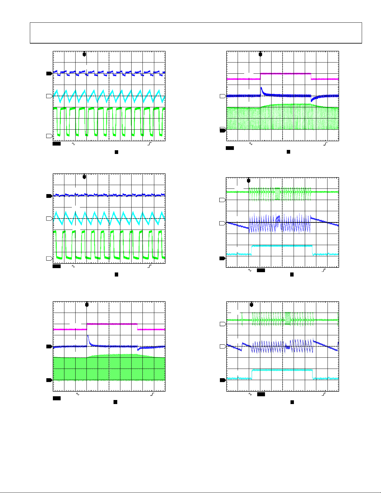
ADP5033
T
T
VOUT
I
SW
SW
VOUT
I
SW
SW
CH2 500mA Ω
CH4 2.00V
T
OUT1
T 28.40%
= 3.3 V, I
= 30 mA, PWM Mode
OUT1
1
2
4
CH1 50mV M 400ns A CH2 220mA
Figure 21. Typical Waveforms, V
1
2
VIN
1
4
3
09788-027
Figure 24. BUCK2 Response to Line Transient, V
4
1
VOUT
SW
CH1 50.0mV
CH3 1.00V CH4 2.00V
= 1.8 V, PWM Mode
V
OUT2
T
SW
VOUT
M 1.00ms A CH3 4.80V
T 30.40%
= 4.5 V to 5.0 V,
IN
09788-013
4
CH1 50mV M 400ns A CH2 220mA
Figure 22. Typical Waveforms, VOUT2 = 1.8 V, I
CH2 500mA Ω
CH4 2.00V
T 28.40%
= 30 mA, PWM Mode
OUT2
09788-026
T
VIN
1
3
VOUT
SW
CH1 50.0mV
CH3 1.00V CH4 2.00V
M 1.00ms A CH3 4.80V
T 30.40%
09788-012
Figure 23. Buck1 Response to Line Transient, Input Voltage from 4.5 V to
5.0 V, V
= 3.3 V, PWM Mode
OUT1
I
OUT
2
CH1 50.0mV
CH2 50.0mA Ω
CH4 5.00V
M 20.0µs A CH2 356mA
T 60.000µs
Figure 25. BUCK1 Response to Load Transient, I
= 3.3 V, Auto Mode
V
OUT1
T
SW
4
VOUT
1
I
OUT
2
CH1 50.0mV
CH2 50.0mA Ω
CH4 5.00V
M 20.0µs A CH2 379mA
T 22.20%
Figure 26. BUCK2 Response to Load Transient, I
V
= 1.8 V, Auto Mode
OUT2
from 1 mA to 50 mA,
OUT1
from 1 mA to 50 mA,
OUT2
09788-016
9788-015
Rev. 0 | Page 11 of 28

ADP5033
T
SW
4
1
VOUT
I
OUT
T
I
2
1
IN
VOUT
EN
2
CH1 50.0mV
CH2 200mA Ω
CH4 5.00V
M 20.0µs A CH2 408mA
T 20.40%
Figure 27. BUCK1 Response to Load Transient, I
V
= 3.3 V, Auto Mode
OUT1
T
SW
4
1
2
CH1 100mV
VOUT
I
OUT
CH2 200mA Ω
CH4 5.00V
M 20.0µs A CH2 88.0mA
T 19.20%
Figure 28. BUCK2 Response to Load Transient, I
= 1.8 V, Auto Mode
V
OUT2
T
VOUT2
2
SW1
from 20 mA to 180 mA,
OUT1
from 20 mA to 180 mA,
OUT2
3
CH1 2.00V M 40.0µs A CH3 2.2V
9788-017
CH3 5.00V
Figure 30. LDO Startup, VOUT3 = 3.0 V, I
2.820
2.815
2.810
2.805
C (V)
2.800
OUT
V
2.795
2.790
2.785
2.780
0 0.05 0.10 0.15 0.20 0.25 0.30
09788-018
Figure 31. LDO Load Regulation Across Input Voltage, V
CH2 50.0mA Ω
I
OUT
T 11.20%
(A)
OUT3
= 5 mA
VIN = 3.3V
VIN = 4.5V
VIN = 5.0V
VIN = 5.5V
OUT3
= 2.8 V
09788-022
09788-046
3.45
3.40
3.35
VIN = 4.2V, +85°C
VIN = 4.2V, +25°C
VIN = 4.2V, –40°C
3
VOUT1
1
4
CH1 5.00V
CH3 5.00V
SW2
CH2 5.00V
CH4 5.00V
M 400ns A C H4 1.90V
T 50.00%
09788-066
Figure 29. VOUT and SW Waveforms for BUCK1 and BUCK2 in PWM Mode
Showing Out-of-Phase Operation
Rev. 0 | Page 12 of 28
D (V)
3.30
OUT
V
3.25
3.20
3.15
000.250.200.150.100.05
I
OUT
(A)
Figure 32. LDO Load Regulation Across Temperature, V
= 3.3 V, V
IN3
.30
09788-049
= 2.8 V
OUT3

ADP5033
3.0
2.5
2.0
C (V)
1.5
OUT
V
1.0
0.5
0
2.4 2.6 2.8 3.0 3.2 3.4 3.6 3.8 4.0 4.2 4.4 4.6 4.8 5.0 5.2 5.4
(V)
V
IN
Figure 33. LDO Line Regulation Across Output Load, V
50
45
40
35
30
25
20
15
GROUND CURRE NT (µA)
10
5
0
0 0.05 0.10 0.15 0.20 0.25
LOAD CURRENT (A)
Figure 34. LDO Ground Current vs. Output Load, V
T
I
OUT
2
I
OUT
I
OUT
I
OUT
I
OUT
I
OUT
I
OUT
= 3.3 V, V
IN3
= 300mA
= 150mA
= 100mA
= 10mA
= 1mA
= 100µA
= 2.8 V
OUT3
OUT3
09788-045
= 2.8 V
2
1
3
CH1 20.0mV
CH3 1.00V
Figure 36. LDO Response to Line Transient, Input Voltage from 4.5 V to 5.5 V,
60
55
50
45
40
RMS NOISE (µV)
35
30
25
0.001 0.01 0.1 1 10 100
09788-136
Figure 37. LDO Output Noise vs. Load Current, Across Input Voltage,
65
60
55
50
VIN
VOUT
T
M 100µs A CH3 4.80V
V
OUT3
T 28.40%
= 2.8 V
09788-014
5VIN
3.3VIN
I
(mA)
V
OUT3
5VIN
3.3VIN
LOAD
= 2.8 V
09788-047
1
Figure 35. LDO Response to Load Transient, I
VOUT
CH1 100mV M 40.0µs A CH2 52.0mA
CH2 100mA Ω
V
OUT3
= 2.8 V
T 19.20%
OUT3
from 1 mA to 80 mA,
09788-019
Rev. 0 | Page 13 of 28
45
40
RMS NOISE (µV)
35
30
25
0.001 0.01 0.1 1 10 100
I
LOAD
(mA)
Figure 38. LDO Output Noise vs. Load Current, Across Input Voltage,
= 3.0 V
V
OUT3
09788-048

ADP5033
0
100µA
–10
1mA
10mA
–20
50mA
100mA
–30
150mA
–40
–50
PSRR (dB)
–60
–70
–80
–90
–100
10 100 1k 10k 100k 1M 10M
Figure 39. LDO PSRR Across Output Load, V
FREQUENCY (Hz )
= 3.3 V, V
IN3
OUT3
= 2.8 V
09788-050
0
100µA
–20
–40
–60
PSRR (dB)
–80
–100
–120
10 100 1k 10k 100k 1M 10M
Figure 41. LDO PSRR Across Output Load, V
1mA
10mA
50mA
100mA
150mA
FREQUENCY (Hz )
= 5.0 V, V
IN3
OUT3
= 2.8 V
09788-053
0
–20
–40
–60
PSRR (dB)
–80
–100
–120
10 100 1k 10k 100k 1M 10M
FREQUENCY (Hz )
Figure 40. LDO PSRR Across Output Load, V
100µA
1mA
10mA
50mA
100mA
150mA
IN3
= 3.3 V, V
OUT3
= 3.0 V
0
–10
–20
–30
–40
–50
PSRR (dB)
–60
–70
–80
–90
–100
09788-051
Figure 42. LDO PSRR Across Output Load, V
100µA
1mA
10mA
50mA
100mA
150mA
10 100 1k 10k 100k 1M 10M
FREQUENCY (Hz )
= 5.0 V, V
IN3
OUT3
= 3.0 V
09788-052
Rev. 0 | Page 14 of 28

ADP5033
P
POWER DISSIPATION AND THERMAL CONSIDERATIONS
The ADP5033 is a highly efficient micropower management
unit (µPMU), and, in most cases, the power dissipated in the
device is not a concern. However, if the device operates at high
ambient temperatures and maximum loading condition, the
junction temperature can reach the maximum allowable
operating limit (125°C).
When the temperature exceeds 150°C, the ADP5033 turns off
all the regulators, allowing the device to cool down. When the
die temperature falls below 130°C, the ADP5033 resumes
normal operation.
This section provides guidelines to calculate the power dissipated in the device and ensure that the ADP5033 operates
below the maximum allowable junction temperature.
The efficiency for each regulator on the ADP5033 is given by
OUT
η
100%×=
P
IN
(1)
where:
η is the efficiency.
P
is the input power.
IN
P
is the output power.
OUT
Power loss is given by
P
= PIN − P
LOSS
(2a)
OUT
or
P
= P
LOSS
(1− η)/η (2b)
OUT
Power dissipation can be calculated in several ways. The most
intuitive and practical is to measure the power dissipated at the
input and all the outputs. Perform the measurements at the
worst-case conditions (voltages, currents, and temperature).
The difference between input and output power is dissipated in
the device and the inductor. Use Equation 4 to derive the power
lost in the inductor and, from this, use Equation 3 to calculate
the power dissipation in the ADP5033 buck converter.
A second method to estimate the power dissipation uses the
efficiency curves provided for the buck regulator, and the power
lost on each LDO can be calculated using Equation 12. When
the buck efficiency is known, use Equation 2b to derive the total
power lost in the buck regulator and inductor, use Equation 4 to
derive the power lost in the inductor, and then calculate the
power dissipation in the buck converter using Equation 3. Add
the power dissipated in the buck and in the two LDOs to find
the total dissipated power.
Note that the buck efficiency curves are typical values and may
, V
not be provided for all possible combinations of V
To account for these variations, it is necessary to include a
I
OUT.
, and
IN
OUT
safety margin when calculating the power dissipated in the buck.
A third way to estimate the power dissipation is analytical and
involves modeling the losses in the buck circuit provided by
Equation 8 to Equation 11 and the losses in the LDO provided
by Equation 12.
Rev. 0 | Page 15 of 28
BUCK REGULATOR POWER DISSIPATION
The power loss of
P
= P
LOSS
where:
P
is the power dissipation on one of the ADP5033 buck
DBU
CK
regulato
P
rs.
is the inductor power losses.
L
The inducto
have any effect on the die temper
The inductor losses are estimated (without core losses) by
P
≈ I
L
where:
DCR
is the inductor series resistance.
L
I
is the rms load curren
)
OUT1(RMS
where r is the inductor ripple cur t
r ≈ V
where:
L is the inductance.
f
is the s
SW
D is the duty cycle.
D = V
ADP5033 buck regu
er switch conductive losses, the switch losses, and the transi-
pow
tion losses of each channel. There are other sources of loss, but
these are generally less significant at high output load currents,
where the thermal limit of the application is. Equation 8
captures the calculation that must be made to estimate the
power dissipation in the buck regulator.
P
DBUCK
The power switch conductive losses are due
, flowing through the P-MOSFET and the N-MOSFET
I
OUT
1
power switches that have internal resistance, RDS
RDS
. The amount of conductive power loss is found by
ON-N
P
COND
where RDS
mate
ly 0.16 Ω at 125°C junction temperature and VIN1 = VIN2 =
3.6 V. At VIN1 = VIN2 = 2.3 V, these values change to 0.31 Ω and
0.21 Ω, respectively, and at VIN1 = VIN2 = 5.5 V, the values are
0.16 Ω and 0.14 Ω, respectively.
the buck regulator is approximated by
DBUCK1
+ P
+ PL
DBUCK2
r losses are external to the device, and they do not
ature.
2
OUT1(RMS)
× DCRL
t of the buck regulator.
II
OUT1
)(1
RMSOUT
(5)
12
r
+1
×=
ren
× (1 − D)/(I
OUT1
× L × fSW) (6)
OUT1
witching frequency.
OUT1/VIN1
= P
lator power dissipation, P
+ PSW + P
COND
TRAN
, includes the
DBUCK
to the output current,
and
ON-P
= [RDS
ON-P
× D + RDS
ON-P
× (1 − D)] × I
ON-N
is approximately 0.2 Ω, and RDS
OUT1
is approx
ON-N
2
i-
(3)
(4)
(7)
(8)
(9)

ADP5033
S
witching losses are associated with the current drawn by the
driver to turn on and turn off the power devices at the switching
frequency. The amount of switching power loss is given by
P
= (C
SW
whe
re:
C
C
the P-MOSFET gate capacitance.
is
GATE-P
is the N-MOSFET gate capacitance.
GATE-N
GATE-P
+ C
GATE-N
For the ADP5033, the total of (C
) × V
2
IN1
GATE-P
× f
SW
+ C
) is approxi-
E-N
GAT
(10)
mately 150 pF.
The transition l
MOSFET cannot be turned on or off instantaneously, and t
osses occur because the P-channel power
he
SW node takes some time to slew from near ground to near
V
(and from V
OUT1
to ground). The amount of transition
OUT1
loss is calculated by
P
= V
TRAN
whe fall time of the
re t
RISE
IN1
and t
switching node, SW. For the ADP5033, the rise and fall time
× (t
× I
T1
OU
are the rise time and the
FALL
RISE
+ t
FALL
) × f
SW
(11)
s of
SW are in the order of 5 ns.
If the preceding equations an
d parameters are used for estimating the converter efficiency, it must be noted that the equations
do not describe all of the converter losses, and the parameter
values given are typical numbers. The converter performance
also depends on the choice of passive components and board
layout; therefore, a sufficient safety margin should be included
in the estimate.
LDO Regulator Power
The power loss of a LDO regulator is gi
P
= [(VIN − V
DLDO
whe
re:
I
V
he load current of the LDO regulator.
is t
LOAD
and V
IN
are input and output voltages of th
OUT
Dissipation
) × I
OUT
LOAD
ven by
] + (VIN × I
) (12)
GND
e LDO,
respectively.
I
is the ground current of the LDO regulator.
GND
Power dissipation due to the ground current is sm
all, and it
can be ignored.
JUNCTION TEMPERATURE
The total power dissipation in the ADP5033 simplifies to
P
= P
D
In cases where the board temperature T
resistance parameter, θ
temperature rise. T
formula
T
= TA + (PD × θJA) (14)
J
The typical θ
57°C/W (see Tabl e 6 ). A very important factor to consider is
that θ
is based on a 4-layer 4 in × 3 in, 2.5 oz copper, as per
JA
JEDEC standard, and real applications may use different sizes
and layers. It is important to maximize the copper used to remove
the heat from the device. Copper exposed to air dissipates heat
better than copper used in the inner layers. The exposed pad
should be connected to the ground plane with several vias.
If the case temperature can be measured, the junction temperature is calculated by
T
= TC + (PD × ΨJB) (15)
J
where T
board thermal resistance provided in Ta ble 6.
When designing an application for a particular ambient
temperature range, calculate the expected ADP5033 power
dissipation (P
Equation 8 to Equation 13. From this power calculation, the
junction temperature, T
The reliable operation of the converter and the two LDO regulators
can be achieved only if the estimated die junction temperature of
the ADP5033 (Equation 14) is less than 125°C. Reliability and
mean time between failures (MTBF) is highly affected by increasing the junction temperature. Additional information about
product reliability can be found in the ADI Reliability Handbook,
which can be found at www.analog.com/reliability_handbook.
+ P
DBUCK
value for the 16-ball, 0.5 mm pitch WLCSP is
JA
is the case temperature and ΨJB is the junction-to-
C
) due to the losses of all channels by using the
D
+ P
DLDO1
, can be used to estimate the junction
JA
is calculated from TA and PD using the
J
, can be estimated using Equation 14.
J
(13)
DLDO2
is known, the thermal
A
Rev. 0 | Page 16 of 28
ADP5033
V
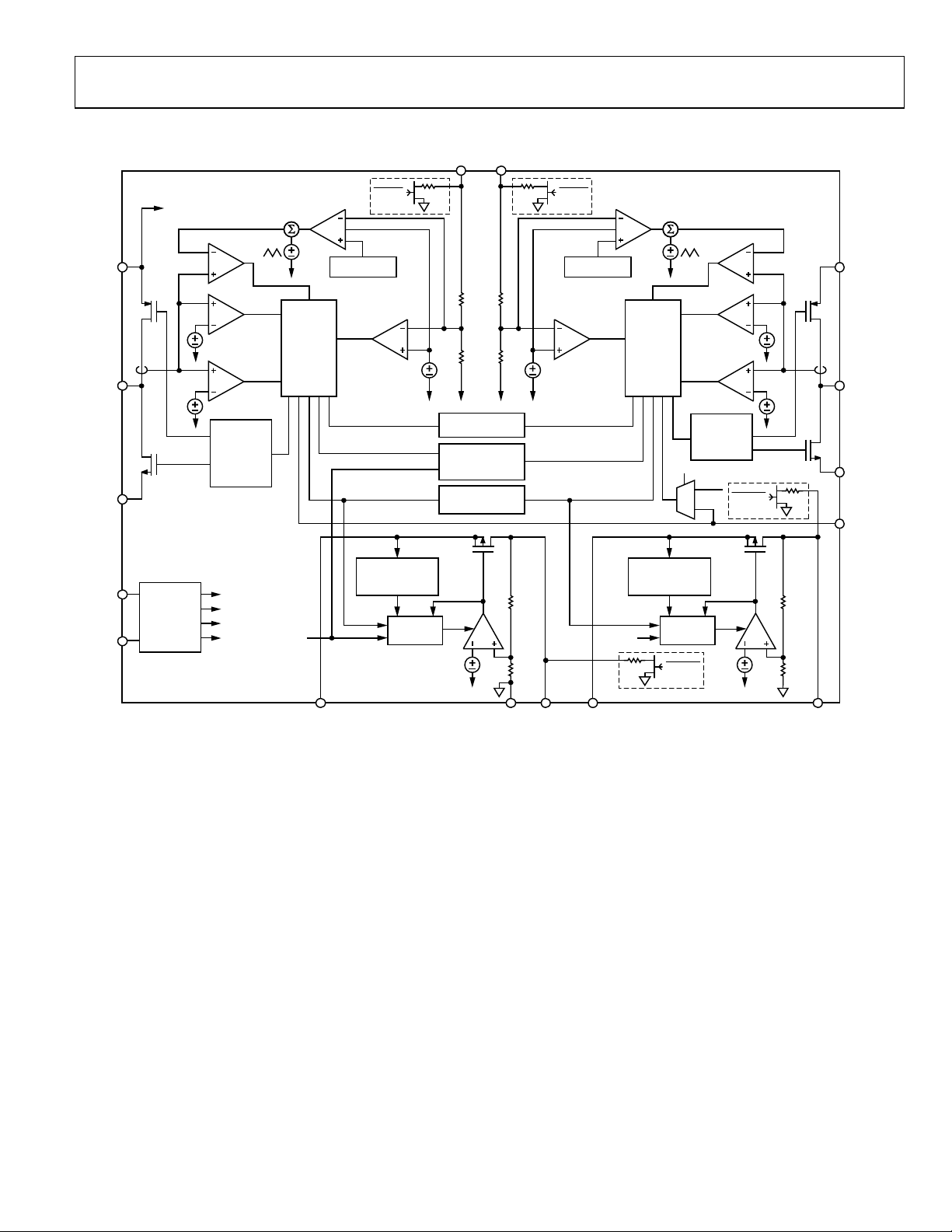
THEORY OF OPERATION
GM ERROR
CONTROL
VDDA
VIN1
SW1
PGND1
ENA
ENB
VDDA
ENABLE
AND MODE
CONTROL
PWM
COMP
I
LIMIT
LOW
CURRENT
DRIVER
AND
ANTISHOOT
THROUGH
ENBK1
ENBK2
ENLDO1
ENLDO2
AMP
PWM/
PSM
BUCK1
ENBK1
SOFT START
PSM
COMP
UNDERVOLTAGE
LOCK OUT
LDO
LDO
CONTROL
OUT1VOUT2
75Ω
OSCILLATOR
UNDERVOLTAGE
SHUTDOWN
SYSTEM
LOCKOUT
THERMAL
R1
R2
75Ω
ENBK2
SOFT START
PSM
COMP
GM ERROR
AMP
PWM/
PSM
CONTROL
BUCK2
UNDERVOLTAGE
LOCK OUT
VDDA
600Ω
OPMODE
SEL
B
Y
A
LDO
LDO
CONTROL
ENLDO1
PWM
COMP
I
LIMIT
LOW
CURRENT
DRIVER
AND
ANTISHOOT
THROUGH
MODE2
ADP5033
ENLDO1
VIN2
SW2
PGND2
600Ω
MODE
R3
R4
VIN3 AGND VOUT3
Figure 43. Functional Block Diagram
POWER MANAGEMENT UNIT
The ADP5033 is a micropower management unit (µPMU)
combing two step-down (buck) dc-to-dc convertors and two
low dropout linear regulators (LDO). The high switching
frequency and tiny 16-ball WLCSP package allow for a small
power management solution.
To combine these high performance regulators into the µPMU,
there is a system controller allowing them to operate together.
The buck regulators can operate in forced PWM mode if the
MODE pin is at a logic high level. In forced PWM mode, the
buck switching frequency is always constant and does not
change with the load current. If the MODE pin is at logic low,
the switching regulators operate in auto PWM/PSM mode.
In this mode, the regulators operate at fixed PWM frequency
when the load current is above the power saving current threshold. When the load current falls below the power save current
threshold, the regulator in question enters PSM where the
switching occurs in bursts. The burst repetition is a
VIN4 VOUT4
function of the current load and the output capacitor value.
This operating mode reduces the switching and quiescent current losses. The auto PWM/PSM mode transition is controlled
independently for each buck regulator. The two bucks operate
synchronized to each other.
When a regulator is turned on, the output voltage ramp is
controlled through a soft start circuit to avoid a large inrush
current due to the charging of the output capacitors.
Thermal Protection
In the event that the junction temperature rises above 150°C,
the thermal shutdown circuit turns off all the regulators. Extreme
junction temperatures can be the result of high current operation, poor circuit board design, or high ambient temperature.
A 20°C hysteresis is included so that when thermal shutdown
occurs, the regulators do not return to operation until the on-chip
temperature drops below 130°C. When coming out of thermal
shutdown, all regulators restart with soft start control.
09788-003
Rev. 0 | Page 17 of 28

ADP5033
Undervoltage Lockout
To protect against battery discharge, undervoltage lockout (UVLO)
circuitry is integrated in the system. If the input voltage on VIN1
drops below a typical 2.15 V UVLO threshold, all channels shut
down. In the buck channels, both the power switch and the
synchronous rectifier turn off. When the voltage on VIN1 rises
above the UVLO threshold, the part is enabled once more.
Alternatively, the user can select device models with a UVLO
set at a higher level, suitable for USB applications. For these
models, the device reaches the turn-off threshold when the
input supply drops to 3.65 V typical.
In case of a thermal or UVLO event, the active pull-downs (if
factory enabled) are enabled to discharge the output capacitors
quickly. The pull-downs remain engaged until the input supply
voltage or thermal fault event is no longer present.
Enable/Shutdown
The ADP5033 has two enable pins (ENA and ENB). A high
level applied to the enable pins enables a certain selection of
regulators defined by factory programming. For example, the
ADP5033 can be factory programmed to enable BUCK1 and
LDO2 with ENA and BUCK2 and LDO1 with ENB. When both
enables are low, all regulators are turned off. When both enable
pins are high, all regulators are turned on. All possible regulator
combinations can be factory programmed to operate with the
ENA and ENB pins.
Figure 44 shows the regulator activation timings for the
ADP5033 when both enables are connected to VINx. Figure 44
also shows the active pull-down activation.
BUCK1 AND BUCK2
The two bucks use a fixed frequency and high speed current
mode architecture. The bucks operate with an input voltage of
2.3 V to 5.5 V.
Control Scheme
The bucks operate with a fixed frequency, current mode PWM
control architecture at medium to high loads for high efficiency
but shift to a PSM control scheme at light loads to lower the
regulation power losses. When operating in fixed frequency
PWM mode, the duty cycle of the integrated switches is adjusted
and regulates the output voltage. When operating in PSM at
light loads, the output voltage is controlled in a hysteretic
manner, with higher output voltage ripple. During part of this
time, the converter is able to stop switching and enters an idle
mode, which improves conversion efficiency.
PWM Mode
In PWM mode, the bucks operate at a fixed frequency of 3 MHz
set by an internal oscillator. At the start of each oscillator cycle,
the pFET switch is turned on, sending a positive voltage across
the inductor. Current in the inductor increases until the current
sense signal crosses the peak inductor current threshold that
turns off the pFET switch and turns on the nFET synchronous
rectifier. This sends a negative voltage across the inductor,
causing the inductor current to decrease. The synchronous
rectifier stays on for the rest of the cycle. The buck regulates the
output voltage by adjusting the peak inductor current threshold.
VIN1
VOUT1
VOUT3
VOUT4
VOUT2
BUCK1, LDO1, L DO2
PULL-DOWNS
BUCK2
PULL-DOWN
VUVLO
30µs (MIN)
50µs (MIN)
Figure 44. Regulators Sequencing on the ADP5033 (ENx = VINx)
VPOR
30µs (MIN)
50µs (MIN)
09788-148
Rev. 0 | Page 18 of 28

ADP5033
PSM
The bucks smoothly transition to PSM operation when the load
current decreases below the PSM current threshold. When
either of the bucks enters PSM, an offset is induced in the PWM
regulation level, which makes the output voltage rise. When the
output voltage reaches a level approximately 1.5% above the
PWM regulation level, PWM operation is turned off. At this
point, both power switches are off, and the buck enters an idle
mode. The output capacitor discharges until the output voltage
falls to the PWM regulation voltage, at which point the device
drives the inductor to make the output voltage rise again to the
upper threshold. This process is repeated while the load current
is below the PSM current threshold.
The ADP5033 has a dedicated MODE pin controlling the PSM
and PWM operation. A high logic level applied to the MODE
pin forces both bucks to operate in PWM mode. A logic level
low sets the bucks to operate in auto PSM/PWM.
PSM Current Threshold
The PSM current threshold is set to100 mA. The bucks employ
a scheme that enables this current to remain accurately controlled, independent of input and output voltage levels. This
scheme also ensures that there is very little hysteresis between
the PSM current threshold for entry to and exit from the PSM.
The PSM current threshold is optimized for excellent efficiency
over all load currents.
Oscillator/Phasing of Inductor Switching
The ADP5033 ensures that both bucks operate at the same
switching frequency when both bucks are in PWM mode.
Additionally, the ADP5033 ensures that when both bucks are in
PWM mode, they operate out of phase, whereby the Buck2
pFET starts conducting exactly half a clock period after the
Buck1 pFET starts conducting.
Short-Circuit Protection
The bucks include frequency foldback to prevent output current
runaway on a hard short. When the voltage at the feedback pin
falls below half the target output voltage, indicating the possibility of a hard short at the output, the switching frequency is
reduced to half the internal oscillator frequency. The reduction
in the switching frequency allows more time for the inductor to
discharge, preventing a runaway of output current.
Soft Start
The bucks have an internal soft start function that ramps the
output voltage in a controlled manner upon startup, thereby
limiting the inrush current. This prevents possible input voltage
drops when a battery or a high impedance power source is
connected to the input of the converter.
Current Limit
Each buck has protection circuitry to limit the amount of
positive current flowing through the pFET switch and the
amount of negative current flowing through the synchronous
rectifier. The positive current limit on the power switch limits
the amount of current that can flow from the input to the
output. The negative current limit prevents the inductor
current from reversing direction and flowing out of the load.
100% Duty Operation
With a dropin input voltage or with an increase in load current,
the buck may reach a limit where, even with the pFET switch
on 100% of the time, the output voltage drops below the desired
output voltage. At this limit, the buck transitions to a mode
where the pFET switch stays on 100% of the time. When the
input conditions change again and the required duty cycle
falls, the buck immediately restarts PWM regulation without
allowing overshoot on the output voltage.
Active Pull-Downs
All regulators have optional, factory programmable, active pulldown resistors discharging the respective output capacitors
when the regulators are disabled by the ENx pins or by a faulty
condition. The pull-down resistors are connected between
VOUTx and AGND. Active pull-downs are disabled when the
regulators are turned on. The typical value of the pull-down
resistor is 600 for the LDOs and 75 for the bucks. Figure 44
shows the activation timings for the active pull-down during
regulator activation and deactivation.
LDO1 AND LDO2
The ADP5033 contains two LDOs with low quiescent current
and two low dropout linear regulators and provides up to
300 mA of output current. Drawing a low 25 A quiescent
current (typical) at no load makes the LDO ideal for batteryoperated portable equipment.
Each LDO operates with an input voltage of 1.7 V to 5.5 V. The
wide operating range makes these LDOs suitable for cascading
configurations where the LDO supply voltage is provided from
one of the buck regulators.
Each LDO also provides high power supply rejection ratio
(PSRR), low output noise, and excellent line and load transient
response with just a small 1 µF ceramic input and output
capacitor.
LDO1 is optimized to supply analog circuits because it offers
better noise performance compared to LDO2. LDO1 should be
used in applications where noise performance is critical.
Rev. 0 | Page 19 of 28
ADP5033
APPLICATIONS INFORMATION
BUCK EXTERNAL COMPONENT SELECTION
Trade-offs between performance parameters such as efficiency
and transient response can be made by varying the choice of
external components in the applications circuit, as shown in
Figure 1.
Inductor
The high switching frequency of the ADP5033 bucks allows for
the selection of small chip inductors. For best performance, use
inductor values between 0.7 H and 3 H. Suggested inductors
are shown in Ta ble 8.
The peak-to-peak inductor current ripple is calculated using
the following equation:
VVV
−×
××
I
RIPPLE
OUT
LfV
2
)(
Dimensions
(mm)
I
SAT
(mA)
DCR
(mΩ)
I
RIPPLE
OUT
=
IN
IN
SW
where:
f
is the switching frequency.
SW
L is the inductor value.
The minimum dc current rating of the inductor must be greater
than the inductor peak current. The inductor peak current is
calculated using the following equation:
II +=
PEAK
)(
MAXLOAD
Inductor conduction losses are caused by the flow of current
through the inductor, which has an associated internal dc
resistance (DCR). Larger sized inductors have smaller DCR,
which may decrease inductor conduction losses. Inductor core
losses are related to the magnetic permeability of the core material.
Because the bucks are high switching frequency dc-to-dc
converters, shielded ferrite core material is recommended for
its low core losses and low EMI.
Table 8. Suggested 1.0 μH Inductors
Vendor Model
Murata LQM2MPN1R0NG0B 2.0 × 1.6 × 0.9 1400 85
Murata LQM18FN1R0M00B 1.6 × 0.8 × 0.8 150 26
Taiyo Yuden BRC1608T1R0M 1.6 × 0.8 × 0.8 520 180
Coil craft® EPL2014-102ML 2.0 × 2.0 × 1.4 900 59
TDK GLFR1608T1R0M-LR 1.6 × 0.8 × 0.8 230 80
Coilcraft 0603LS-102 1.8 × 1.69 × 1.1 400 81
Toko MDT2520-CN 2.5 × 2.0 × 1.2 1350 85
Output Capacitor
Higher output capacitor values reduce the output voltage ripple
and improve load transient response. When choosing this value,
it is also important to account for the loss of capacitance due to
output voltage dc bias.
Ceramic capacitors are manufactured with a variety of dielectrics, each with a different behavior over temperature and
applied voltage. Capacitors must have a dielectric adequate
to ensure the minimum capacitance over the necessary
temperature range and dc bias conditions. X5R or X7R
dielectrics with a voltage rating of 6.3 V or 10 V are recommended for best performance. Y5V and Z5U dielectrics are
not recommended for use with any dc-to-dc converter because
of their poor temperature and dc bias characteristics.
The worst-case capacitance accounting for capacitor variation
over temperature, component tolerance, and voltage is calculated using the following equation:
= C
C
EFF
× (1 − TEMPCO) × (1 − TOL)
OUT
where:
is the effective capacitance at the operating voltage.
C
EFF
TEMPCO is the worst-case capacitor temperature coefficient.
TOL is the worst-case component tolerance.
In this example, the worst-case temperature coefficient
(TEMPCO) over −40°C to +85°C is assumed to be 15% for an
X5R dielectric. The tolerance of the capacitor (TOL) is assumed
to be 10%, and C
is 9.24 F at 1.8 V, as shown in Figure 45.
OUT
Substituting these values in the equation yields
= 9.24 F × (1 − 0.15) × (1 − 0.1) = 7.074 F
C
EFF
To guarantee the performance of the bucks, it is imperative
that the effects of dc bias, temperature, and tolerances on the
behavior of the capacitors be evaluated for each application.
12
10
8
6
4
CAPACITANCE (µF)
2
Rev. 0 | Page 20 of 28
0
0123456
DC BIAS VOLTAGE (V)
Figure 45. Typical Capacitor Performance
09788-004

ADP5033
The peak-to-peak output voltage ripple for the selected output
capacitor and inductor values is calculated using the following
equation:
V
RIPPLE
SW
IN
CLf
××××
22
OUT
=
()
π
RIPPLE
SW
CfI××=8
OUT
V
Capacitors with lower equivalent series resistance (ESR) are
preferred to guarantee low output voltage ripple, as shown in
the following equation:
V
RIPPLE
ESR ≤
COUT
I
RIPPLE
Table 9. Suggested 10 μF Capacitors
Vendor Type Model Case Size Voltage Rating (V)
Murata X5R GRM188R60J106 0603 6.3
Taiyo Yuden X5R JMK107BJ475 0603 6.3
TDK X5R C1608JB0J106K 0603 6.3
Panasonic X5R ECJ1VB0J106M 0603 6.3
The effective capacitance needed for stability, which includes
temperature and dc bias effects, is a minimum of 7 µF and a
maximum of 40 µF.
The buck regulators require 10 µF output capacitors to guarantee stability and response to rapid load variations and to
transition into and out of the PWM/PSM modes. In certain
applications, where one or both buck regulators power a
processor, the operating state is known because it is controlled
by software. In this condition, the processor can drive the
MODE pin according to the operating state; consequently, it is
possible to reduce the output capacitor from 10 µF to 4.7 µF
because the regulator does not expect a large load variation
when working in PSM mode (see Figure 47).
Rev. 0 | Page 21 of 28

ADP5033
Input Capacitor
Higher value input capacitors help to reduce the input voltage
ripple and improve transient response. Maximum input
capacitor current is calculated using the following equation:
−
VVV
CIN
IN
≥
II
OUT
)(
MAXLOAD
V
IN
OUT
)(
To minimize supply noise, place the input capacitor as close
to the VINx pin of the buck as possible. As with the output
capacitor, a low ESR capacitor is recommended.
The effective capacitance needed for stability, which includes
temperature and dc bias effects, is a minimum of 3 µF and a
maximum of 10 µF. A list of suggested capacitors is shown in
Tabl e 1 0 .
Table 10. Suggested 4.7 μF Capacitors
Voltage
Rating
Vendor Type Model
Murata X5R GRM188R60J475ME19D 0402 6.3
Taiyo Yuden X5R JMK107BJ475 0402 6.3
Panasonic X5R ECJ-0EB0J475M 0402 6.3
Case
Size
(V)
LDO CAPACITOR SELECTION
Output Capacitor
The ADP5033 LDOs are designed for operation with small,
space-saving ceramic capacitors, but function with most
commonly used capacitors as long as care is taken with the ESR
value. The ESR of the output capacitor affects the stability of the
LDO control loop. A minimum of 0.70 µF capacitance with an
ESR of 1 Ω or less is recommended to ensure the stability of the
ADP5033. Transient response to changes in load current is also
affected by output capacitance. Using a larger value of output
capacitance improves the transient response of the ADP5033 to
large changes in load current.
Input Bypass Capacitor
Connecting a 1 µF capacitor from VIN3 and VIN4 to ground
reduces the circuit sensitivity to printed circuit board (PCB)
layout, especially when long input traces or a high source
impedance is encountered. If greater than 1 µF of output
capacitance is required, increase the input capacitor to match it.
Table 11. Suggested 1.0 μF Capacitors
Vendor Type Model
Murata X5R GRM155B30J105K 0402 6.3
TDK X5R C1005JB0J105KT 0402 6.3
Panasonic X5R ECJ0EB0J105K 0402 6.3
Taiyo Yuden X5R LMK105BJ105MV-F 0402 10.0
Case
Size
Input and Output Capacitor Properties
Use any good quality ceramic capacitors with the ADP5033 as
long as they meet the minimum capacitance and maximum ESR
requirements. Ceramic capacitors are manufactured with a
Voltage
Rating (V)
variety of dielectrics, each with a different behavior over
temperature and applied voltage. Capacitors must have a
dielectric adequate to ensure the minimum capacitance over the
necessary temperature range and dc bias conditions. X5R or
X7R dielectrics with a voltage rating of 6.3 V or 10 V are
recommended for best performance. Y5V and Z5U dielectrics
are not recommended for use with any LDO because of their
poor temperature and dc bias characteristics.
Figure 46 depicts the capacitance vs. voltage bias characteristic
of a 0402 1 µF, 10 V, X5R capacitor. The voltage stability of a
capacitor is strongly influenced by the capacitor size and voltage
rating. In general, a capacitor in a larger package or higher voltage
rating exhibits better stability. The temperature variation of the
X5R dielectric is about ±15% over the −40°C to +85°C temperature range and is not a function of package or voltage rating.
1.2
1.0
0.8
0.6
0.4
CAPACITANCE ( µF)
0.2
0
01 2345 6
Figure 46. Capacitance vs. Voltage Characteristic
DC BIAS VOLTAGE ( V)
09788-006
Use the following equation to determine the worst-case capacitance accounting for capacitor variation over temperature,
component tolerance, and voltage:
C
= C
EFF
× (1 − TEMPCO) × (1 − TOL)
BIAS
where:
is the effective capacitance at the operating voltage.
C
BIAS
TEMPCO is the worst-case capacitor temperature coefficient.
TOL is the worst-case component tolerance.
In this example, the worst-case temperature coefficient
(TEMPCO) over −40°C to +85°C is assumed to be 15% for an
X5R dielectric. The tolerance of the capacitor (TOL) is assumed
to be 10%, and C
is 0.94 F at 1.8 V, as shown in Figure 46.
BIAS
Substituting these values into the following equation,
= 0.94 F × (1 − 0.15) × (1 − 0.1) = 0.719 F
C
EFF
Therefore, the capacitor chosen in this example meets the
minimum capacitance requirement of the LDO over
temperature and tolerance at the chosen output voltage.
To guarantee the performance of the ADP5033, it is imperative
that the effects of dc bias, temperature, and tolerances on the
behavior of the capacitors be evaluated for each application.
Rev. 0 | Page 22 of 28

ADP5033
PCB LAYOUT GUIDELINES
Poor layout can affect ADP5033 performance, causing electromagnetic interference (EMI) and electromagnetic compatibility
(EMC) problems, ground bounce, and voltage losses. Poor
layout can also affect regulation and stability. A good layout is
implemented using the following guidelines:
• Place the inductor, input capacitor, and output capacitor
close to the IC using short tracks. These components carry
high switching frequencies, and large tracks act as antennas.
• Route the output voltage path away from the inductor and
SW node to minimize noise and magnetic interference.
• Maximize the size of ground metal on the component side
to help with thermal dissipation.
• Use a ground plane with several vias connecting to the
component side ground to further reduce noise interference on sensitive circuit nodes.
• Connect VIN1 and VIN2 together close to the IC using
short tracks.
Rev. 0 | Page 23 of 28

ADP5033
A
TYPICAL APPLICATION SCHEMATIC
VIN:
2.3V TO 5.5V
FROM VIO
(1.7V MIN)
C1
4.7µF
ALWAYS ON
ON
OFF
C2
4.7µF
C3
1µF
VIN1
ENA
ENB
VIN2
VIN3
DP5033
BUCK1
ACT
BUCK2
LDO1
BK1
BK2
LD1
LD2
SW1
VOUT1
PGND1
MODE
SW2
VOUT2
PGND2
VOUT3
L1 1µH
L2 1µH
VCORE
C5
4.7µF
VIO
C6
4.7µF
C7
1µF
PROCESSOR
VCORE
GPIO
VIO
ANALOG
SUBSYSTEM
VANA
FROM VCORE
(1.7V MIN)
1µF
VIN4
C4
LDO2
AGND
VOUT4
C8
1µF
VDIG
09788-152
Figure 47. Processor System Power Management with PSM/PWM Control
Rev. 0 | Page 24 of 28

ADP5033
OUTLINE DIMENSIONS
0.660
0.602
0.544
SEATING
PLANE
0.330
0.310
0.290
1.50
REF
3
4
12
A
B
C
BALL 1
IDENTIFIER
2.12
2.08 SQ
2.04
0.022
REF
0.50
TOP VIEW
(BALL SIDE DOWN)
0.380
0.352
0.324
0.04 NOM
COPLANARITY
0.280
0.250
0.220
REF
Figure 48. 16-Ball Wafer Level Chip Scale Package [WLCSP]
Back-Coating Included
(CB-16-7)
Dimensions shown in millimeters
ORDERING GUIDE
ENA
Temperature
Model1
Range
ADP5033ACBZ-1-R7 −40°C to +125°C VOUT1: 1.2 V
ADP5033-1-EVALZ
1
Z = RoHS Compliant Part.
2
For additional options, contact a local sales or distribution representative. Additional options available are
BUCK1 and BUCK2: 3.3 V, 3.0 V, 2.8 V, 2.5 V, 2.3 V, 2.0 V, 1.82 V, 1.8 V, 1.6 V, 1.5 V, 1.3 V, 1.2 V, 1.1 V, 1.0 V, 0.9 V, 0.8 V.
LDO1 and LDO2: 3.3 V, 3.0 V, 2.9 V, 2.8 V, 2.775 V, 2.5 V, 2.0 V, 1.875 V, 1.8 V, 1.75 V, 1.7 V, 1.65 V, 1.6 V, 1.55 V, 1.5 V, 1.2 V.
UVLO: 2.25 V or 3.9 V.
Active pull-down: Yes/No.
3
ENA activated channels (ENB controls the other channels).
Output
Voltage (V)2 Options
UVLO: 2.25 V
VOUT2: 3.3 V
VOUT3: 2.8 V
Pull-Downs on
All Channels
VOUT4: 1.8 V
Controlled
Channels3
BUCK2,
LDO1
Package
Description
16-Ball Wafer Level
Chip Scale
Package [WLCSP]
Evaluation Board
BOTTOM VIEW
(BALL SIDE UP)
D
013009-B
Package
Option
Branding
Code
CB-16-7 LHX
Rev. 0 | Page 25 of 28

ADP5033
NOTES
Rev. 0 | Page 26 of 28

ADP5033
NOTES
Rev. 0 | Page 27 of 28

ADP5033
NOTES
©2011 Analog Devices, Inc. All rights reserved. Trademarks and
registered trademarks are the property of their respective owners.
D09788-0-5/11(0)
Rev. 0 | Page 28 of 28
 Loading...